Embed Size (px)
Citation preview

國 立 交 通 大 學
材料科學與工程學系
碩 士 論 文
研究藉由氧化鋁為閘極絕緣層來改善成長於矽
基板上之氧化鋁鎵氮化鎵高電子遷移率電晶體
之線性度
Study of AlGaNGaN MOS-HEMTs on Silicon Substrate with
Al2O3 Gate Insulator for Device Linearity Improvement
研 究 生陳玉芳
指導教授張翼 博士
中 華 民 國 一百 年 十 月
I
研究藉由氧化鋁為閘極絕緣層來改善成長於矽基板上之氧化鋁鎵
氮化鎵高電子遷移率電晶之線性度
Study of AlGaNGaN MOS-HEMTs on Silicon Substrate with Al2O3 Gate Insulator for Device Linearity Improvement
研究生 陳玉芳 指導教授 張翼 博士
國立交通大學材料科學與工程學系
摘要
近年來氮化鎵高電子移動率電晶體具有優越的特性使其在高功率高溫高崩潰
偏壓以及高頻應用有很大的潛力然而在高功率無線通訊遇到關鍵性難題就是以複雜
調變技術來達成高速率傳輸的目的時此調變技術會導致動態訊號的產生進而造成訊
號失真因此在射頻功率放大器中元件線性度成為無線通訊系統中一項非常重要的參
數在本研究中金氧半氮化鎵高電子移動率電晶體與一般傳統的蕭基閘極氮化鎵高電
子移動率電晶體相較擁有較好的元件線性度特性與較高的通道飽和電流本研究成功
製作出 15 微米閘極線寬的三氧化二鋁金氧半氮化鎵高電子移動率電晶體並且將其電
性分析與一般傳統的蕭基閘極氮化鎵高電子移動率電晶體相比證實元件在線性度上有
顯著的改善本論文研究顯示三氧化二鋁金氧半氮化鎵高電子移動率電晶體能有效的
增進元件之線性度有效地應用在無線通訊系統中的射頻功率放大器
II
Study of AlGaNGaN MOS-HEMTs on Silicon Substrate with
Al2O3 Gate Insulator for Device Linearity Improvement
Student Yu-Fang Chen Advisor Dr Edward Yi Chang
Department of Materials Science and Engineering
National Chiao Tung University
Abstract Superior properties of AlGaNGaN HEMTs are promising contenders for
high-power high-temperature high-breakdown and high-frequency applications
and have attracted much attention recently However one of the key issues for
using AlGaNGaN HEMTs for high-power radio-frequency (RF) applications is
the quality of the transiting signals For the modern wireless communication
here are many users and the neighboring frequencies are usually located closely
to each other Hence it is important to suppress the signal distortions for the
device used in the communication system could not induce signal distortions A
among all intermodulation distortions third-order intermodulation distortion
(IM3) usually cannot be filtered out by the filter therefore IM3 dominates the
linearity performance of the device and is the most important linearity criteria
for wireless communication system In this study itrsquos found that MOS-HEMT
exhibits better linearity and higher channel saturation current compared to the
HEMTs with Schottky-gate In this paper we present the linearity characteristics
of the Al2O3 AlGaNGaN MOS-HEMTs on Si substrates with gate length 15μm
and compare it with the regular AlGaNGaN HEMTs devices for device linearity
improvement in this study
III
誌謝
碩士班兩年的時光有開心瘋狂大笑也有遇到挫折低潮到真思考休學回頭想想真
慶幸我熬了過來在張翼老師的帶領下我們猶如在業界快速的學習與成長學了製
程所需的所有機台體驗到團體生活從不熟陌生到熟稔這些是在別的實驗室無法
獲得與體會的一路過來謝謝幫助過我的人謝謝曾經有的挫折謝謝張翼老師努力
不懈研究爭取實驗室資源還有耐心的幫我們即將畢業的學生一頁頁修改我們的論文
謝謝林岳欽學長一路以來的指導與幫助陪我們熬夜量測事事替我們著想還犧牲假
日來當我的口試委員也謝謝 Fiaz 的幫助讓我成功的換組沒有你我想我應該碩班當博
班念吧hellip更謝謝一路一起奮鬥過來的黃大頭跟阿澤沒有你們的陪伴與幫助我想我做
實驗真的會很無聊跟孤單尤其謝謝明明已經畢業的黃大頭有情有義留下來幫我與阿
澤幫我們改論文量測畫圖還一起熬夜我真的非常非常感謝你唷謝謝阿澤一
路上的包容與耐心雖然你後來見色忘友的很厲害我還是很謝謝你唷~謝謝幫我長氧
化層的 Dang如果不是你精湛的長成技術我是無法有如此好得數據可以畢業也謝
謝我以前的指導教授倪澤恩老師沒有你我真的無法考上交大謝謝你在我最低潮的
時候總是耐心的開導我告訴我該如何做謝謝王人正學長當初大學時候研究訓練
與高壓下的學習總是刀子嘴豆腐心的帶領我們真的萬般的感激你你結婚的時候我
一定會包大包一點啦謝謝我的正妹室友林妍君沒有你的陪伴與貼心的關懷我想我
真的會悶到爆炸希望你早日找到如意郎君謝謝我的家人一路上無條件的相挺與包容我
的壞脾氣還讓我無後顧之憂的念書我會趕快出去賺錢回饋你們的^^謝謝劉臭臭一路
上包容我的壞脾氣還耐心聽我抱怨與帶我去出飯即使我在怎麼任性還是會願意挺我
與聽我抱怨謝謝老皮阿伯當初的教導沒有你們那兩個月紮實的訓練我無法成為
機台小天后謝謝林芝羽總是無條件的挺我替我擔心我真得很高興能夠遇到你這樣的
麻吉我們再一起去土地公還願吧以後還是可以常打給我唷要堅強不要傻傻被欺負唷~
謝謝阿韋賤賤的關懷與貼心叮嚀謝謝宗運學弟的體貼與諒解讓我無後顧之憂的專心
IV
弄論文謝謝長褲學弟的幫忙與協助讓我跟阿澤可以專心的準備口試謝謝一路玩耍
瘋狂的婉儀林緯佑誠沒有你們我碩一生活無法如此的精彩與快樂謝謝哲榮一
路上的相挺與關懷明明是學長卻總是被我兇hellip謝謝已經畢業的凱麟與培維與你們
相處的時光真的很歡樂凱麟的包容與冷靜的解析給我意見恭喜你交到人生第一個女
朋友好感謝電子所 418 陪我走過來的所有人謝謝你們總是忍受我聒噪吵鬧謝謝張
俊彥校長默默的縱容我與關心謝謝張嘉華學長總是幫忙我預約量測沒我聊天打
屁在我口試前一天晚上還幫忙我修改投影片與畫圖謝謝延儀每次都在我報告的時候
幫我修改英文文法還有忍受我三不五十的找麻煩謝謝大家雖然總是嗆我損我卻
又總是在我傷心難過的時候無條件的挺我與幫我謝謝總是被我機車態度激到快發瘋
其實很貼心又細心的谷銘謝謝細心與貼心總是笑笑的庭維謝謝一臉認真講話很好笑
的智翔謝謝看起來臉臭臭可是很讚的學弟宗運我真的沒有覺得你很不好啦你們真
得很乖唷颱風天還願意來學習以後要好好加油努力喔謝謝我的麻吉黃老人總是在
我低潮難過陪我聊天還努力幫我物色好男人謝謝太多要謝謝的人謝謝你們如果
沒有被我提出來不代表我沒有謝謝你們喔不要生氣呢謝謝大家~我終於終於可以下
台一鞠躬囉~喔耶喔耶
V
Contents Abstract inChinese I
Abstract in English II
Acknowledgement III
Contents V
Table Captions VIII
Figure Captions IX
Chapter 1
Introduction
11 General background and motivation 1
12 Scope and organization of thesis 3
Chapter 2
AlGaNGaN Metal-Oxide-Semicomductor HEMTs
21 Material properties of GaN 5
22 Polarization effect of GaN 6
221 Crystal structure and piezoelectric polarization 7
222 Strain-induced piezoelectric and spontaneous polarization 8
23 AlGaNGaN High Electron Mobility Transistors 8
VI
231 Hetero epitaxial growth of AlGaNGaN HEMTs 8
232 The basic and operation of AlGaNGaN HEMTs 10
233 Issues of high gate leakage current AlGaNGaN HEMTs 11
24 AlGaNGaN Metal-Oxide-Semiconductor HEMTs 12
241 Introduction 12
242 The requirements of high-k insulator oxide 13
Chapter 3
Fabrications of AlGaNGaN MOS-HEMTs with Al2O3 High-K Gate Oxide
31 Ohmic Contact Formation 22
32 Mesa isolation 23
33 Atomic layer deposition (ALD) Al2O3 24
34 Gate Formation 25
Chapter 4
Fundamentals of HEMT Electrical Characteristics
41 DC Characteristics Measurement 29
42 Transmission Line Model (TLM) 30
43 Linearity 31
44 Breakdown Voltage (BVgd) 32
VII
45 Extrinsic Transconductance (gm) 33
46Scattering Parameters 34
47 Current-Gain Cutoff Frequency (fT) and Maximum Oscillation Frequency
( fmax) 35
Chapter 5
Study of AlGaNGaN MOS-HEMTs on Silicon substrate with Al2O3 Gate
Insulator for Device Linearity Improvement
51 Introduction 41
52 Device fabrication 43
53 Results and discussion 44
54 Conclusions 49
Chapter 6
Conclusion
Conclusions 63
Reference 65
VIII
Table Captions
Chapter 2
Table 21 Advantages of GaN material for electronic applications 15
Table 22 Material properties and figure of merit (FOM) of GaN 4H-SiC GaAs
and Si at 300K for microwave power device applications All FOMs
are normalized with respect to those Si 15
Table 23 Comparison of 2DEG mobility and sheet carrier concentration of
AlGaNGaN structure grown by MOCVD and MBE on different
substrates The carrier mobility and concentration are measured at 300
77 42 or 03 K unless specify in the bracket x is the Al content in
AlGaN layer 16
Table 24 Comparison of the proportion of different gate oxides properties 17
Chapter 5
Table 51 Comparison of the IP3 values of Al2O3 MOS-HEMT and HEMT
devices at 7 volt drain bias 62
IX
Figures Caption
Chapter 1
Fig 11 Commercial and military markets targeted by GaN 4
Chapter 2
Fig 21 Band gap (Eg) versus lattice constant at 300 K for wurtzite (α-phase)
and zincoblende (β-phase) GaN InN and AlN The right-hand scale
gives the light wavelength corresponding to the band gap energy 17
Fig 22 Semiconductor materials for RF electrons applications 18
Fig 23 Electron drift velocity of GaN SiC Si and GaAs at 300 K computed
using the Monte Carlo Method 18
Fig 24 Schematic drawing of the structures and energy band structures of
wurtzite GaN and Zinc Blende GaN 19
Fig 25 Schematic of the crystal structure of wurtzite Ga-face and-face GaN
The spontaneous polarization (Psp) direction is also shown 19
Fig 26 Polarization induced sheet density and directions for the spontaneous
and piezoelectric polarization in Ga- and N-face AlNGaN
heterostructures 20
Fig 27 Basic structure and its band diagram of AlGaNGaN HEMT 20
Fig 28 Structure comparisons between AlGaNGaN HEMT (on the left) and
Al2O3 HEMT (MOS-HEMT) (on the right) 21
Fig 29 Energy band gap versus Insulator constant diagram of oxides 21
X
Chapter 3
Fig 31 Schematic of the whole wafer before prepare 26
Fig 32 Schematic of the wafer after Ohmic contact formation 26
Fig 33 Schematic of the wafer after Mesa isolation 27
Fig 34 Schematic of the wafer after Atomic layer deposition (ALD) Al2O3 27
Fig 35 Schematic of the wafer after Gate formation 28
Chapter 4
Fig 41 The Transmission Line Method (TLM ) pattern 38
Fig 42 The illustration of utilizing TLM to measure ohmic contact resistance 38
Fig 43 Output power diagram of fundamental and third-order product signal
39
Fig 44 Fundamental diagram of the microwave front-end device 39
Fig 45 The equivalent two-port network schematic at high frequency 40
Fig 46 AlGaNGaN HEMT intrinsic device model 40
Fig 47 AlGaNGaN HEMT small signal equivalent circuit 40
Chapter 5
Fig 51 Cross section of the (a) 15μm a Schottky-gate AlGaNGaN HEMT (b)
MOS-HEMT with 10nm Al2O3 51
Fig 52 DC ID versus VDS characteristics at VGS= 1 to -6 V of the AlGaNGaN
HEMT and Al2O3 MOS-HEMT 52
XI
Fig 53 IDS versus VGS curve for the AlGaNGaN HEMT and Al2O3
MOS-HEMT at the 7 volt VDS bias 53
Fig 54 Transconductance gm versus gate-source bias VGS at the same drain bias
Vds = 7V in the saturation region for the AlGaNGaN HEMT and Al2O3
MOS-HEMT with gate length =15μm 54
Fig 55 Gate leakage currents for the AlGaNGaN HEMT and Al2O3
MOS-HEMT with the same device dimensions 55
Fig 56 Off-state drain-source breakdown characteristics of Al2O3 MOS-HEMT
and regular-HEMTs 56
Fig 57 IDS versus VGS curves for the AlGaNGaN HEMT and Al2O3
MOS-HEMT at the VDS bias from 4 V to 7 V 57
Fig 58 Gm versus VGS curve for the AlGaNGaN HEMT and Al2O3
MOS-HEMT at the VDS bias from 4 V to 7 V 58
Fig 59 IDS versus VGS curve for the Al2O3 MOS-HEMT at the VDS bias from
4 V to 10 V 59
Fig 510 Gm versus VGS curve for the Al2O3 MOS-HEMT at the VDS bias from
4 V to 10V 60
Fig 511 IP3 versus IDS curve of the the AlGaNGaN HEMT and Al2O3
MOS-HEMT the test frequency is 2GHz and VDS =7V 61
1
Chapter 1
Introduction
11 General Background and Motivation
The wide spread communication systems such as third-generation (3G)
mobile systems wireless LAN electronic toll collection system (ETC) and
global positioning system (GPS) Recently wide band-gap semiconductors have
attracted considerable attentions as the next generation materials for RF power
electronic applications such as mobile satellites and cable TV systems[1] for
power transmitter applications In the mobile communication applications the
next generation cell phone need widen bandwidth and higher efficiencies also
the development of satellites communication and TV broadcasting systems also
require amplifiers which can operate at higher frequencies and higher power
Because of these demands the outstanding properties of AlGaNGaN HEMTs
make them most promising candidate for microwave power applications in the
wireless communication Some of the commercial and military markets that are
targeted by GaN devices are shown in Fig 11
However for the microwave monolithic integrated circuits (MMICs) for
power applications a major problem is to increase the operating frequency One
of the major factors limited the performance of the GaN HEMT devices is the
high gate leakage current due to the surface defects of the devices and finite
barrier height of the Schottky gate This gate leakage problem becomes more
serious when dealing with high-power and high-temperature RF applications
For this reason to improve the device high frequency performance the lowest
2
possible gate leakage current level must be achieved The use of high-k gate
insulator for AlGaNGaN MOS-HEMT can significantly suppress the
direct-tunneling gate current
In the past few years many studies regarding of about the III-Vhigh-k
interface issues have been published It is well known that the surface
pretreatment including sulfide and ammonia solution treatments could eliminate
the undesired particles and native oxides Furthermore the surface of III-V
material could be passivated by the treatment to prevent the surface exposed to
air With the progress of advanced deposition technologies many passivation
methods had been reported including Gd2O3Ga2O3 or SiNx as gate insulators
the Al2O3 growth by atomic layer deposition (ALD) [2-4] Among all the
deposition technologies the ALD shows superior characteristics for oxides
deposited ALD has several advantages over other techniques due to the actual
mechanism used to deposit the films ALD is especially advantageous when film
quality or thickness is critical ALD is also quite effective to be deposited at
coating ultra high aspect ratio substrates or substrates that would be difficult to
coat with other thin film techniques It can achieve the high purity level than any
other deposition technologies In this study the ALD system was used for the
high-k oxide deposition
The main purpose of this study is to establish the AlGaNGaN MOS-HEMT
devices technology with low leakage current for high power high frequency
applications The technology include the applications of ALD Al2O3 with a high
insulator constant (86-10) and a high breakdown field (5~10 MVcm) for the
gate insulators for AlGaNGaN MOS-HEMTs The RF and DC performances of
the AlGaNGaN HEMTs with gate oxide in this study will be evaluated in this
thesis
3
12 Organization of the Thesis
This thesis is comprised of six chapters including conclusions After
background introduction the GaN material properties and operation principle of
HEMTs will be introduced in chapter 2 The AlGaNGaN MOS-HEMTs device
fabrication process is introduced in chapter 3 In Chapter 4 the electrical
characterization methods for AlGaNGaN MOS-HEMTs are described Chapter
5 is the experiment results and discussion of the performance AlGaNGaN
MOS-HEMTs on Si substrate compared to regular HEMT Finally the
conclusions will be given in chapter 6
4
Fig 11 Commercial and military markets targeted by GaN
5
Chapter 2
AlGaNGaN Metal-Oxide-Semiconductor HEMTs
An overview on GaN material and AlGaNGaN HEMTs will be presented
in this chapter Material properties of GaN especially the unique characteristics
for electronic applications are introduced first This is followed by a brief
description of the polarization effect of GaN along with AlGaNGaN HEMTs
Thereafter the AlGaNGaN MOS HEMT which is the focus of this study is
discussed The historical approaches for the gate insulator of GaN MOS devices
are reviewed and the device advantages of MOS-HEMTs over Schottky-gate
HEMTs are highlighted Finally the basic operation and the non-ideal
phenomena of MOS HEMTs are introduced
21 Material properties of GaN
GaN-based materials GaN indium nitride (InN) and aluminum nitride
(AlN) are wide bandgap semiconductors They are the candidates for next
generation high power devices These materials have several advantages such as
high band gap high electron velocity and high breakdown electric field The
bandgaps of GaN InN and AlN are respectively 34 eV 189 eV and 62 eV as
shown in Fig 21 The figure not only shows the wide range of energies of III-V
nitride materials but also shows the wavelengths from the visible-light to the
ultraviolet (UV) regions if they are used for optical devices Thus three-nitrides
are good candidates for optoelectronic devices such as light emission diodes
(LEDs) laser diodes (LDs) detectors and so on
6
Compared with other III-V semiconductor materials GaN gains a
considerable attention for the RF power application Fig 22 compared the
power vs frequency performance of GaN in comparison with other
semiconductors and it indicates that III-V nitrides materials GaN are promising
candidates for the RF power application Besides due to the strong bonding
energy between the Ga and N GaN has a high breakdown field at about 33
MVcm which means the GaN devices can withstand high operating voltage
Although GaN has the lower room temperature electron mobility around
1500cm2Vs than that of GaAs GaN has very high electron saturation velocity
about 3times107 cm2s This suggests the high frequency applications of the
GaN-based devices Moreover GaN has a high thermal conductivity around 13
Wcmk this makes it possible to operate at high temperatures The benefits of
GaN for electronic applications are listed in Table 21 Table 22 and Fig 23
show the material properties and figures of merit of GaN compared with the
competing material such as 4H-SiC GaAs and Si According to the outstanding
material properties of GaN GaN-based devices are the good candidates in
high-power high-frequency high speed and high-temperature applications
22 Polarization effect of GaN
The polarization effects in GaN are due to two types one is strain-induced
piezoelectric polarization and the other is spontaneous polarization The
strain-induced piezoelectric polarization is resulted from the lattice mismatch
and the spontaneous polarization is due to the noncentrosymmetry of the
wurtzite GaN and large iconicity of the covalent GaN bonds The crystal
7
structure induced polarization of GaN then the strain-induced piezoelectric and
spontaneous polarization will be described in next section
221 Crystal structure and piezoelectric polarization [5]
GaN-based materials have two crystal structure hexagonal wurtzite
structure and cubic zinc blends as shown in Fig 24 Since there is no native
GaN substrate GaN-based materials are grown on the other substrate such as
sapphire and silicon carbide Recently GaN growth on Si substrate is
well-explored SiC and sapphire are hexagonal structure and Si is diamond
cubic structure In general if noncentrosymmetric compound crystals have two
different sequences of the atomic layering in the two opposing directions
parallel a certain crystallographic axes crystallographic polarity along these
axes can be observed In early 90rsquos the role of nucleation layer was discovered
and (0001) GaN was growth on (0001) sapphire After that hexagonal
GaN-based materials are widely used in LED and HEMT structure These are
two different growth directions lead GaN to nonequivalent surfaces of Ga- or N-
faced In Ga-face the Ga atoms are on the top position of bilayers
corresponding to the [0001] polarity On the other hand in N-face the N atoms
are located on the surface of 0001 corresponding to the [0001] polarity Fig
25 shows two different crystal planes of hexagonal GaN lattice structure
According to the specific crystallographic polarities GaN exhibits different
chemical and physical properties
222 Strain-induced piezoelectric and spontaneous polarization [5]
8
In case of Ga-face of GaN shown in Fig 25 the spontaneous polarization
PSP direction is downward to the substrate In the other word the polarization in
N-face of GaN in Fig 25 is in opposite direction to Ga-face In addition GaN
has piezoelectric spontaneous polarization PPE result from the lattice mismatch
between AlGaN and GaN The PPE can be calculated by piezoelectric constants
e33 and e31 elastic constants c13 and c 33 and the lattice parameters a0 is given
by equation
(2-1)
where a is the lattice constant of GaN along a-axis and a0 is equilibrium value
of lattice constant (a- a0)a represents the in-plan strain along a-axis Since
[ ] is less than zero For AlGaN over the whole range of
compositions piezoelectric polarization is positive for compressive and negative
for tensile barriers On the other hand the spontaneous polarization of GaN and
AlN is negative Fig 26 shows the directions of the spontaneous and
piezoelectric polarization in Ga- and N- face strained and relaxed AlGaNGaN
heterostrucutre
23 AlGaNGaN HEMTs
231 Hetero-epitaxial growth of AlGaNGaN HEMTs
Due to the lack of large-size and low-cost commercial-grade substrate GaN
materials are usually grown on the foreign substrates such as sapphire Si or SiC
Table 22 shows some of the material properties of these substrates as compared
9
to the GaN and AlN layers Generally the lattice constants and thermal
expansion coefficients of these substrates differ significantly (except SiC) from
that of GaN The first successful epitaxial layer layers of GaN were grown on
Sapphire However the very large lattice mismatch (148) and the difference
in the thermal expansion coefficient between GaN and sapphire substrate cause
the huge challenges in the grown of nitrides As a result of these mismatches
large amount of dislocations are generated in the GaN film The quality of the
GaN film is therefore critically dependent on the ability of the transition layer
(buffer layer) used to accommodate the stress generated from these mismatches
The commonly used buffer layers include low temperature GaN [6-7] AlN
[8-10] or their variations [11-13] Dislocations generated in GaN are mainly
screw edge and mixed TDs In addition to the buffer layers other approaches
are also used to improve the crystal quality of GaN film such as the insertion of
AlN interlayers [14] or Si delta-doping layer [15]
High crystalline quality GaN materials are usually grown by metal-organic
chemical vapor deposition (MOCVD) and molecular beam epitaxy (MBE)
methods MOCVD is famous for growing the LED-quality GaN and is also used
to grow GaN materials for HEMT applications lately The main advantages of
MOCVD as compared to MBE are the high growth rate and high crystal
quality even for the direct growth of GaN layers on the foreign substrates
Besides MBE has also proven to be a promising technique to grow GaN
materials for HEMT devices application [16-18] The benefits of growing GaN
by MBE include real-time monitoring of crystal growth with reflection
high-energy electron deflection (RHEED) a carbon-free and hydrogen-free
growth environment a smooth surface sharp interfaces and low point defect
density These attributes are important for achieving high quality materials for
10
HEMT devices Table 23 lists some important developments on the electrical
properties of AlGaNGaN structure grown by MOCVD and MBE techniques
Although these difficulties have been solved the low thermal conductivity
is still an unneglectable problem Compared with sapphire SiC has less lattice
mismatch (4) with GaN and very good thermal properties which is nearly 10
times more than that of sapphire Therefore SiC is rather popular substrate Yet
SiC is too expensive for commercialization Recently GaN HEMTs grown on Si
substrate was been widely investigated due to lower material cost and
compatible with Si technology for circuit integration
232 The Basic Structure and Operation of AlGaNGaN HEMTs
GaN materials for HEMT fabrication consists of a higher bandgap material
such as AlGaN [19] or AlInN [20] grown on the top of the GaN film as the
barrier layer The discontinuity in conduction bands between the two materials
forms a 2-dimentional electron gas (2DEG) channel at the hetero-interface
Basic GaN HEMT structure and band diagrams are shown in Fig 27
AlGaNGaN HEMT 2DEG formation is totally different from GaAs HEMT In
AlGaAsGaAs HEMT the channel electrons come from the surface states in the
AlGaAs The electrons in the AlGaAs where driven into the GaAs layer
because the hetero-junction created by different band-gap materials The
formation mechanism of GaN HEMT 2DEG is due to the strong polarization
effect and large amount of surface states High electron density (~15x1013 cm-2)
can be induced at the 2DEG by AlGaN barrier layer with Al~25 and high
electron mobility (~2000 cm2Vs) can be achieved on an AlGaNGaN
heterostructure Therefore AlGaNGaN HEMT does not require intentional
11
doping in the barrier to provide carrier in the 2DEG channel The 2DEG enables
better electron confinement and less carrier scattering Due to both high mobility
and high carrier density AlGaNGaN HEMT device of high current density (gt2
Amm) has been demonstrated [21]
233 Issues of High Gate Leakage Current AlGaNGaN HEMTs
Despite the impressive device performance the potential of AlGaNGaN
HEMTs for commercial application have not been fully realized as yet The RF
power expected from fundamental nitride material properties significantly
exceeds the experimental data One of the key problems limiting the HEMT RF
power is the high Schottky-gate leakage current which results in the degradation
of DCRF parameters At positive gate bias high forward gate current can shunt
the gate-channel capacitance thus limiting the maximum drain current At
negative gate bias high voltage drop between the gate and drain results in
premature breakdown and the maximum applied drain voltage is restricted [22]
In addition gate leakage currents increase the device sub-threshold currents
which decrease the achievable amplitude of the RF output All these limitations
become even more severe at high ambient temperatures Mechanisms of the high
gate leakage current in AlGaNGaN HEMTs have been investigated and
possible solutions to suppress the leakage have been explored in the past few
years Through numerical simulations and DC electrical measurements Miller et
al reported found that vertical tunneling through the gate area is the dominant
mechanism for gate leakage in AlGaN-barrier HEMTs while additional leakage
current mechanisms such as lateral tunneling and defect-assisted tunneling also
contributed to the total gate leakage [23] To suppress the high gate current
12
Miller et al proposed an enhanced-barrier HEMT structure in which a GaN cap
layer was grown on the top of the standard AlGaN barrier Owing to the strong
polarization effects in the nitrides the peak barrier height in the new
GaNAlGaNGaN HEMT was increased thus decreasing the tunneling gate
leakage current Mizuno et al compared the gate leakage current of a
GaN-based HEMT with a GaAs-based HEMT [24] They observed both a two to
three orders of magnitude larger gate leakage of the GaN-based HEMTs as
compared to that of the GaAs-based HEMTs and the temperature-independence
for the gate leakage current in GaN-based HEMTs Considering that AlGaN has
a larger Schottky barrier height (14 eV) than GaAs HEMTs (~10 eV) the
authors attributed tunneling to be the main leakage mechanism instead of the
thermionic emission They also found that surface treatment with CF4 plasma
prior to the gate metal deposition was able to reduce the gate leakage current by
two to three orders of magnitude A possible explanation of such leakage
suppression is that the plasma treatment introduces deep acceptors to
compensate the high-density positive charge on the AlGaN surface Thus the
depletion layer thickness under the gate increases and gate leakage current due
to electron tunneling becomes small
24 AlGaNGaN MOS HEMTs
241 Introduction
As described above device performance of conventional Schottky gate
AlGaNGaN HEMT device suffers from high gate leakage current As a result
13
the drain current collapse when operating at high-frequency and poor long-term
reliability of Schottky gate In order to reduce the gate leakage current a
concept of high-k insulators layers between gate metal and semiconductor were
investigated in the past years A schematic comparison between HEMT and
MOS-HEMTs for AlGaNGaN is illustrated in Fig 28
242 The requirements of high-k insulators oxide
(A) Insulator constant
Insulator constant is the most important parameter for oxide material used in
the MOS structure Due to the reduction of chiprsquos size in the future the
horizontal electrical field is increased and the gate modulation ability is
decreased In order to solve these problems the capacitance per unit area must
be improved to decrease the effect of undesired electrical field
(2-2)
where C is capacitance Q is charges and V is turned on voltage
ε C (2-3)
where ε is the insulator constant of oxide A is cross section area and d is the
distance between the two plates According to Eq (2-2) the devices with larger
accumulation capacitance can be turn on more easily by a smaller voltage Using
smaller operating voltage will result in higher device efficiency and cost saving
According to the Eq (2-3) the MOS device which using oxide material with
larger insulator constant as its gate insulator will have larger accumulation
capacitance So the high-k oxide is desired for III-V MOS devices technology
The energy band gap versus insulator constants of different oxide materials is
14
plotted depicted in Fig 29
(B) Energy band gap
The energy band gap of oxide materials is an important factor which
influences the leakage current of the MOS devices The oxide with smaller
energy band gap causes the carrier tunneling more easily it will induce
undesired leakage current and influence the devices performance The oxide
with larger energy band gap can prevent the carriers tunneling But the oxide
with higher insulator constant will have the smaller energy bandgap So it is
important to find the suitable oxide to improve the MOS devices performance
Several gate oxide candidates are listed in Table 24 Besides the band offset of
oxide on semiconductor material is also needed to be considered the value must
exceed 1 eV so that the oxide can serve an effective insulator [18]
ALD Al2O3 is introduced in this study due to its relatively high band gap
(about 87 eV) and remains amorphous under typical processing conditions In
addition Al2O3 also possesses high breakdown electric field (5~20 MVcm)
high thermal stability (up to 1000) and strong adhesion with dissimilar
materials [25] With well-controlled thickness and uniformity for the Al2O3 layer
deposited by ALD technology by the good insularity of Al2O3 layer ALD Al2O3
is the leading candidate for the gate insulators in MOS-HEMT device
15
Table 21 Advantages of GaN material for electronic applications
Material property Advantages Wide bandgap 342 eV
Great endurance for high device operating temperature Suitable for high power applications Working under high temperature environment
+High breakdown field 4times106 Vcm
Larger power density
High thermal conductivity ~13Wcm K
Better heat dissipation enhanced device performance Easier device packaging
High saturate electron velocity ~27times107 cmsec
Suitable for high frequency applications
Table 22 Material properties and figure of merit (FOM) of GaN 4H-SiC GaAs
and Si at 300K for microwave power device applications All FOMs are
normalized with respect to those Si
Material Bandgap Energy
(eV)
Breakdown field
(MVcm)
Thermal conductively (WKcm)
Electron mobility
(cm2Vs)
High-field Peak velocity
(times107cms)
GaN 340 40 13 1350 27 4H-SiC 326 30 49 800 20 GaAs 142 04 05 6000 20
Si 112 025 15 1300 10
16
Table 23 Comparison of 2DEG mobility and sheet carrier concentration of
AlGaNGaN structure grown by MOCVD and MBE on different substrates The
carrier mobility and concentration are measured at 300 77 42 or 03 K unless
specify in the bracket x is the Al content in AlGaN layer
Growth Method substrate
Al content
2DEG mobility (cm2Vs) (Sheet carrier concentration (ns (cm-2)) Reference
x 300K 77K 42K 03K
MO
CV
D
SiC 02 2000 (1times1013)
9000 (8times1012)
11000 (7times1012)
Gaska et al (1999) [23]
SiC 04 1990 (14times1013)
Higashiwaki et al (2008) [24]
Sapphire 018 10300 (15K)
(69times1012) Wang et al (1999)
[25]
Sapphire 03 1300 (984times1012)
Liu et al (2006) [26]
Sapphire 02 1700 (84times1012)
Tuumllek et al (2009) [27]
Silicon 026 1500 (82times1012)
Selvaraj et al (2009) [28]
Silicon 1800
(1times1013) Arulkumaran et al
(2010) [29]
MB
E
SiC 03 1500 (1times1013)
Corrion el al (2006) [16]
Sapphire 019 1500 (9times1012)
10310 (6times1012) 12000 Li et el (2000)
[12]
Sapphire 03 1310 (1times1013)
Manfra et al (2002) [10]
Silicon 025 1500 (79times1012)
Dumka et al (2004) [30]
MOCVD-GaNsapphire 009 24000
(25times1012)60000 (4K) (225times1012)
Elsass et al (2000) [31]
MOCVD-GaNsapphire 028 2039
(1times1013) Cordier et al (2007) [32]
HVPE-GaN sapphire 006
80000 (175times1012)
Manfra et al (2004) [33]
Dislocation free-GaN sapphire
01 2500 (26times1012) 109000 Skierbiszewski el
al (2005) [34]
17
Table 24 Comparison of the gate oxidersquos properties
Fig 21 Band gap (Eg) versus lattice constant at 300 K for wurtzite (α-phase)
and zincoblende (β-phase) GaN InN and AlN The right-hand scale gives the
light wavelength corresponding to the band gap energy
18
Fig 22 Semiconductor materials for RF applications
Fig 23 Electron drift velocity of GaN SiC Si and GaAs at 300 K computed
using the Monte Carlo technique
19
Fig 24 Schematic drawing of the crystal and energy band structure of wurtzite
GaN and Zinc Blende GaN
Fig 25 Schematic of the crystal structure of wurtzite Ga-face and-face GaN
The spontaneous polarization (Psp) direction is also shown
Psp
Psp
20
Fig 26 Polarization induced sheet density and directions for the spontaneous
and piezoelectric polarization in Ga- and N-face AlNGaN heterostructures
Fig27 Basic structure and its band diagram AlGaNGaN HEMT
21
Fig 28 Structure comparisons between AlGaNGaN HEMT (on the left) and
Al2O3 HEMT (MOS-HEMT) (on the right)
Fig 29 Energy band gap versus Insulator constant diagram of oxides
22
Chapter 3
Experimental Methods of AlGaNGaN MOS-HEMTs with
Al2O3 High-K Gate Oxide
The fabricated AlGaNGaN MOS-HEMT with Al2O3 high-k gate oxide in this
study brings together a novel design to enhance the electronic properties of the
devices the process flow of AlGaNGaN MOS-HEMT with Al2O3 high-K gate
oxide fabrication in this study includes several steps as shown in Fig 31 and
they are
1 Ohmic contact formation
2 Active region definition (Mesa isolation)
3 Atomic layer deposition (ALD) Al2O3
4 Gate formation
31 Ohmic Contact Formation
An ohmic contact is a low resistance junction formed in between metal and
semiconductor The purpose of an ohmic contact on semiconductor is to allow
the electrical current to flow in and out of the semiconductor A good ohmic
contact is important for a better device performance such as lower power
consumption low noise and so on An ohmic contact should obey the ohms law
that is it should have a linear I-V characteristic either under forward or reverse
bias Therefore to obtain a low resistance ohmic contact we have to create a
23
heavily doped interface between metal and semiconductor In addition an ohmic
contact not only should be stable over time and temperature but also should
have as small resistance
First the negative photoresist AZ5214E and I-line aligner were used to define
the ohmic metal pattern after wafer cleaning by using ACE and IPA Unlike the
Si-based devices the lift-off process is used for III-V based device because of
the lack of appropriate etching selection between ohmic metals and III-V
materials The undercut profile of the negative photoresist AZ5214E will benefit
the metal lift-off process Then the wafers underwent O2 plasma descum to
remove residual photoresist and the dipped in HClH2O (14) solution for 15 s to
remove the native oxide on the GaN surface before Ohmic metallization ohmic
metal was composed of TiAlNiAu from the bottom to the top and it was
deposited by e-gun beam evaporation system Finally tcontacts were annealed
by rapid thermal annealing (RTA) at 850 for 30s in N2 atmosphere after metal
lift-off process as shown in Fig 31 The specific contact resistance was checked
by the transmission line method (TLM) in the process control monitor (PCM) It
containing a linear array of metal contacts with various spacings between them
The distances between TLM electrodes are 3 μm 5 μm 10 μm 20 μm and 36
μm respectively in this study In general the typical measured contact resistance
must be less than 1 x 10⁻⁵ Ω- 2
32 Mesa isolation
For III-V devices the mesa isolation is to isolated devices from each other In
these specific areas the current flow is restricted to the desired path In addition
24
parasitic capacitance parasitic resistance and leakage current can all be reduced
with effective isolation A successful isolation provides sufficient insulating area
to form passive elements such as transmission lines capacitors pads etc
First the active areas were masked by Shipley S1818 photoresist and then the
dry etch process was conducted by inductive couple plasma (ICP) with Cl2 in Ar
ambient After the dry etch process the etching depth should reach the buffer
layer as shown in Fig 33 Finally the photoresist was striped by ACE
According to the device structure the mesa was etched to the buffer layer to
provide good device isolation Finally the etching depth was approximately
2500Aring measured by p-10 surface profiler after the strip of photoresist and the
etching profile was carefully checked by scanning electron microscopy (SEM)
33 Atomic layer deposition (ALD) Al2O3
In this study the Al2O3 was deposited by ALD system ALD developed in
Finland by T Suntolan in 1974 and this method is considered as an advanced
variant of the CVD technique
Before the Al2O3 deposition the chemical surface treatment was used to
remove the surface native oxides Firstly the wafers were immersed by HCl
H2O (14) solution to remove the native oxides and followed by rinsing in the
water for 30 s and blowing dry by N2 gas Then the wafer was directly
immersed in (NH4)2S solution for 15 min at room temperate and also rinsed for
30 s in water and blown dry by N2 gas after (NH4)2S treatment After the
chemical surface treatments the wafer was loaded into the ALD chamber The
Al2O3 films (TMAN2H2ON2 with periods of 02s5s02s5s) were deposited
25
over 50 cycles and the thickness Al2O3 was about 10 nm as shown in Fig 34
Finally the post deposition annealing (PDA) was used to improve the interface
quality The PDA was performed at 400 for 5 min in N2
34 Gate Formation
Schottky barrier gate is one of the most important elements of the HEMTs
Both the dimension length and placement of the gate are very critical For high
speed and high frequency applications short gate length is desired Decreasing
gate length (Lg) can increase the electronic field under the gate so as to
accelerate the transport property of channel electron
In this study the 15 μm gate length was defined by AZ 2020 photoresist
and then the remnant photoresist was removed by ICP with Ar and O2 ambient
Beside the wafer was dipped into the HClH2O (14) solution for 15 s to remove
the negative oxidation before the gate metal deposition Here the multilayer
gate metals TiPtAu were deposited by the e-gum system Finally the wafer was
immersed into the ACE for 30 min to lift ndashoff the undesired metal and the ICP
was used to clean the wafer as shown in Fig 35
26
Fig 31 the whole wafer
Fig 32 Ohmic contact formation
27
Fig 33 Mesa isolation
Fig 34 Atomic layer deposition (ALD) Al2O3
28
Fig 35 Gate formation
29
Chapter 4
Fundamentals of Electrical Characteristization
After the device fabrication DC and RF performances of the AlGaNGaN
HEMT and MOS-HEMT were evaluated by using on-wafer measurement For
the DC measurement the I-V characteristics were obtained by using an
HP4142B Modular DC sourcemonitor and SUSS PA200 semi-auto probe
station The TLM method was used for determining specific contact resistance
was by the 4-wires measurement The S-parameters were measured by
HP8510XF vector network analyzer using on-wafer GSG probes from Cascade
MicroTech However evaluating the RF behaviors of a device on a wafer was a
complicated process For conventional RF measurement of a packaged device
the wafer needs to be diced and then an individual die should be mounted into a
text fixture Discriminating between the diersquos and the fixturersquos responses became
an issue Furthermore fixturing die was a time-consuming process making it
impractical for high-volume screening On-wafer RF characterization can
simplify the process [26]
The method of characterization of the AlGaNGaN HEMT and MOS-HEMT
devices are stated in the following section In this study de-embedding which
must also be performed to obtain the true RF performance of the device is also
performable
41 DC Characteristics Measurment [27]
Before RF performance analysis DC measurement was performed to
30
evaluate the device characteristics including the saturation drain current (Idss)
threshold voltage (Vth) transconductance (Gm) breakdown voltage (VBK) For
IDS-VDS curve the drain voltage sweeps from 0 to 10V and the gate voltage is
from 1 to pinch-off voltage with a step of -1V For IDS-VGS curve the gate
voltage sweeps from 6V to pinch-off voltage such as -8V for MOS-HEMT and
-6 for Schottky-gate HEMT and the drain voltage is from 4 to 15V The
measured breakdown voltage in this study is off-state breakdown voltage The
gate bias is pinch-off voltage and the drain bias sweep from 0 to a specific
value
42 TLM Method
The specific contact resistance between contact metal and cap layer can be
extracted by the TLM method [28] The TLM pattern as illustrated in Fig 41
was designed in the process control monitor (PCM) In this particular approach
a linear array of contacts pad is fabricated with various spacing in between them
The distances between TLM electrodes are 3 5 10 20 and 36 μm respectively
The resistance between the two adjacent electrodes can be plotted as a function
of the space between electrodes and is expressed by the following equation
R = 2Rc +Rs L W (4-11)
where R is measured resistance RC is contact resistance RS is sheet resistance of
channel region W is electrode width and L is the space between electrodes As
Fig 42 shows extrapolating the data to L=0 one can calculate a value for the
term RC And the specific contact resistance ρC can be further extracted by the
following formula
SRRW
C
22
=ρ (4-12)
31
43 Linearity
Linearity of amplifiers is often assessed by the third-order intercept point
(IP3) If an amplifier is presented with two signals closely spaced in frequency
and a perfectly linear amplifier would simply amplify the two signals However
the real amplifier is never with perfectly linearity and nonlinearity will result in
additional output signals A nonlinear amplifier will have a transfer function that
can be approximated as
Po = a1Pin + a2P2in + a3P3
in + hellip (4-13)
where Pin and Po are the input and output power and ai are coefficients A linear
amplifier would have ai =0 for i gt1 Consider an input signal with two closely
spaced frequencies f1 and f2
Pin = P1sin(2πf1t) + P2sin(2πf2t) (4-14)
If Eq (4-14) were substituted into Eq (4-13) we can use elementary
algebra and trigonometric identities to show that the output power (Po) contains
the following components
tfPa 111 2sin π
tfPa 221 2sin π (fundamentals)
tfPa )2(2sin21
12
12 π
tfPa )2(2sin21
22
22 π (second-order products)
tffPPa )2(2sin43
2122
13 plusmnπ
32
tffPPa )2(2sin43
2122
13 plusmnπ (third-order products)
M Assuming P1 = P2 second-order product power is proportional to the square
of the input signal power third-order product power is proportional to the cube
of the input signal power and so on But only the odd and greater than
third-order terms have greater attribution to the fundamental signal So we
usually consider the fundamental signal and the third-order product signal only
Fig 43 is the output power diagram of the fundamental and the third-order
product signals From Fig 43 we can identify the third-order intercept point
(IP3) The Pin value of IP3 is also called IIP3 which is important for low noise
amplifier From the fundamental diagram of microwave front-end device (Fig
44) the low noise amplifier is used to receive signals So a higher IIP3 value
results in a higher linearity of the amplifier and the less distortion of the input
signals
44 Breakdown Voltage (BVgd)
Breakdown mechanisms and models have been discussed in many articles
One of the models showing it is dominated by the thermionic filed emission
(TFE) tunneling current from the Schottky gate This model predicts that the
two-terminal breakdown voltage is lower at higher temperature because
tunneling current increases with the temperature Higher tunneling current
occurs at higher temperature because carriers have higher energy to overcome
the Schottky barrier Other model suggests that impact-ionization determines the
33
final two-terminal breakdown voltage because the avalanche current decreases
with increasing temperature Lower avalanche current occurs at higher
temperature because phonon vibrations as well as carrier-carrier scattering
increase with increasing temperature Either model is incomplete since coupling
exists between TFE and impact ionization mechanisms In addition different
devices may suffer from different breakdown mechanisms depending on the
details of the device design (insulator thickness recess channel composition
and so forth) In this study the gate-to-drain breakdown voltage BVgd is defined
as the gate-to-drain voltage when the gate current is 1mAmm
45 Extrinsic Transconductance (gm)
The transconductance of the HEMTs indicates the ability of the gate voltage
on the control of the drain current It can be defined as
(4-15)
where the vsat is the electron velocity of the ldquotwo dimensional electron gasrdquo
(2-DEG)
The measurement requires specification of the initial gate voltage the gate
voltage step and the drain voltage at which the measurement is made Because
of the nonlinear behavior of source-drain current as a function of gate voltage
gm typically will become less as the bias approaches pinch-off approaches This
also means that a smaller voltage step will yield a higher transconductance The
extrinsic transconductance is a function of the total gate width of the device so
the width must also be given Besides gm may also be normalized to a unit gate
satGG
Dm vZ
ddVdIg
2
2ε==
34
width usually mSmm
46 Scattering Parameters [3-2]
Generally the Scattering parameters which referred to as S-parameters are
fundamental to microwave measurement S-parameters are a way of specifying
return loss and insertion loss or insertion gain Fig 45 shows the equivalent
two-port network schematic at high frequency The relation of the microwave
signals and s-parameters are defined as follows
⎥⎦
⎤⎢⎣
⎡⎥⎦
⎤⎢⎣
⎡=⎥
⎦
⎤⎢⎣
⎡
aa
ssss
bb
21
22211211
21 (4-16)
S signals going into or coming out of the input port are labeled by a
subscript 1 Signals going into or coming out of the input port are labeled by a
subscript 2 The electric field of the microwave signal going into the component
ports is designated a that leaving the ports is designated b Therefore
a1 is the electric field of the microwave signal entering the component input
b1 is the electric field of the microwave signal leaving the component input
a2 is the electric field of the microwave signal entering the component output
b2 is the electric field of the microwave signal leaving the component output
By definition then
0211
11=
=aa
bs
0212
21=
=aa
bs
35
0121
12=
=aa
bs
0122
22=
=aa
bs (4-17)
Consequently s11 is the electric field leaving the input divided by the
electric field entering the input under the condition that no signal enters the
output Because b1 and a1 are electric fields their ratio is a reflection coefficient
Similarly s21 is the electric field leaving the output divided by the electric field
entering the input when no signal enters the output Therefore s21 is a
transmission coefficient and is related to the insertion loss or the gain of the
device s22 is similar to s11 but looks in the other direction into the device
47 Current-Gain Cutoff Frequency (fT) and Maximum Oscillation
Frequency ( fmax)
The intrinsic device model for the HEMT device is shown in Fig 46 If we
only consider the intrinsic part the current can be expressed as
2
22
1
21
2
2
12
1
11
1
VyVyi
VyVyi
+=
+= (4-18)
assume (ωCgsRi)2 ltlt 1 then we can get
36
)(
)(
)(
)(
)(
2211
21
1
2
22
21
12
2211
gdgsigs
migsgdm
dsgdd
mgsgdm
gd
gdgsigs
CCjRC
GRCCjG
yy
ii
CCjGy
GCCjGy
Cjy
CCjRCy
++
+minus==
++=
+minus=
minus=
++=
ωω
ω
ω
ω
ω
ωω
(4-19)
assume igsgdgs
migsgdm
RCCC
GRCCG22)(
|)(|
ωω
ω
gtgt+
+gtgt
fT is defined as the frequency when current gain 11
2 =ii and can be
expressed as
)(2 gdgs
mT CC
Gf
+cong
π (4-20)
fmax can be obtained by using unilateral gain
di
T
digs
m
U
GRff
GRCG
f
yyyyGU
141
1)2
(141
)Re()Re(4||
2
2
22
22
11
212
21
max
=
=
minus==
π (4-21)
when U=1 fmax can be expressed as
di
T
GRff
2max = (4-22)
If we further consider gate resistance Rg ohmic contact resistance Rs and Rd
then the small signal equivalent circuit is shown as Fig 47 assume 1)( 2 ltltigs RCω
37
igsgdgs
migsgdm
RCCC
GRCCG22)(
|)(|
ωω
ω
gtgt+
+gtgt
|)(| dsgddm CCjGG ++gtgt ω
then mgd GCjyyyyY ωcongminus= 21
12
22
11
||
Transfer y parameter into Z parameter
sd
s
s
sg
RRYy
Z
RYyZ
RYyZ
RRYyZ
++=
+minus
=
+minus
=
++=
||||
||
||
11
22
21
21
12
12
22
11
and 21122211|| ZZZZZ minus=
mgddgdgssdgdgs
m
mgddsgddgdgssdgdgs
mgddsgddgdgssm
sd
s
GCjGCCjRRCCjG
ii
GCjCCjGCCjRRCCjGCjCCjGCCjRG
YRRyYRy
ZZZ
Z
yy
ii
ωωω
ωωωωωωω
+++++cong
+++++++
+++++minus=
+++minus
===
)]([)()(
)]()][([)()()]()][([
||)(||
||
||
1
2
11
21
22
21
11
21
1
2
)(])(1)[(2 sdmgddsdgdgs
mT RRGCGRRCC
Gf
+++++cong
π (13)
and we can get fmax [28]
2
max
)1)(52
1(54)
1(4 sm
gs
gd
gs
gd
sm
gsim
m
d
T
RGC
CCC
RGRR
RGGG
ff
++++
++
= (14)
fT and fmax are parameters often used to indicate the high frequency
capability of the transistors
38
Fig 41The Transmission Line Method (TLM ) pattern
Fig 42 The illustration of utilizing TLM to measure ohmic contact resistance
39
-30 -25 -20 -15 -10 -5 0 5 10 15-120
-100
-80
-60
-40
-20
0
20
40
60
3rd ORDER PRODUCTS
FUNDAMENTALS
3rd ORDER INTERCEPT POINT
OP1dB
OIP3
O
utpu
t Pow
er (d
Bm
)
Input Power (dBm)
Fig 43 Output power diagram of fundamental andthird-order product signals
Duplexer
AntennafRF
fIF
fLO
LNA Filter Mixer IF amplifier
Signalprocesscircuit
Modulator
PA Pre-amplifier
LO
Fig 44 Fundamental diagram of the microwave front-end device
40
Fig 45 The equivalent two-port network schematic at high frequency
G D
S S
V 1 V 2 g smVG
d sCdG
gsC
gdC
iR
g sV I 2I1
Fig 46 AlGaNGaN HEMT intrinsic device model
G D
S S
gR gdC
gsV1I
1ViR
gsCdsC
dG
dR
2I
gsmVG2V
sR
Fig 47 AlGaNGaN HEMT small signal equivalent circuit
41
Chapter 5
Study of AlGaNGaN MOS-HEMTs on Silicon substrate with
Al2O3 Gate Insulator for Device Linearity Improvement
As shown in chapter 2 device performance of conventional Schottky-gate
AlGaNGaN HEMTs suffers from high gate leakage current Also the drain
current collapses occurs when operating at high bias voltage resulting in poor
long-term reliability of the Schottky gate To improve the leakage characteristics
of the conventional Schottky-gate AlGaNGaN HEMTs devices the fabrication
and characterization of the 15-μm AlGaNGaN MOS-HEMTs with 10 nm Al2O3
high-k gate oxide grown by ALD on Si substrate was investigated Compared to
regular HEMT devices of similar geometry little degradation of the drain
current and gate control ability was observed The result indicates that
AlGaNGaN MOS-HEMTs were the gate leakage currents several orders of
magnitude lower than those of regular HEMTs and exhibit better linearity
higher channel saturation current with improved higher power performance
51 Introduction
Recently with the rapid development of wireless communication system
the transmission speeds of next-generation wireless mobile networks including
Mobile Worldwide Interoperability for Microwave Access (WiMAX) and long
term evolution (LTE) networks will be several tens of megabits per second
Higher speeds will require increased output power leading to increased power
42
consumption by transmission amplifiers so base stations will require
significantly higher power and more physical space Therefore there is a need to
develop compact base stations that offer easy implementation and low operation
costs To make possible a small base station with lower power consumption
high-efficiency power amplifiers are currently being developed using gallium
nitride high electron mobility transistors (GaN-HEMTs) The superior properties
of AlGaNGaN HEMTs promising contenders for high-power high-temperature
high-breakdown and high-frequency applications
However one of the key problems limiting the performance and reliability
of AlGaNGaN HEMTs for high-power RF applications is the high
Schottky-gate leakage current which results in the degradation of DCRF
parameters At positive gate bias high forward gate current can shunt the
gate-channel capacitance thus limiting the maximum drain current At negative
gate bias high voltage drops between the gate and drain resulting in premature
breakdown and the maximum applied drain voltage is restricted Besides gate
leakage current increase resulting in the device sub-threshold currents which
decrease the achievable amplitude of RF output All these limitations become
the most important key factors to be solved for the development of the advanced
wireless communication system
To overcome this problem several groups have been trying to integrate the
MOS structure into conventional Schottky-gate HEMT by looking for proper
gate insulators for AlGaNGaN based HEMT Al2O3 has been used as the gate
insulator to reduce the gate leakage which allows the application of high
positive gate voltage to further increase the sheet electron density in 2D channel
It also offers additional benefits of a wide band gap (about 87eV) high
breakdown electric field (5~20 MVcm) high thermal stability (amorphous up to
43
at least 1000ordmC) and chemical stability compared to AlGaN With
well-controlled thickness and uniform Al2O3 layer deposited by ALD technology
which employs surface saturation reaction technique ALD Al2O3 is the leading
candidate for the gate insulators in MOS-HEMT device
On the other hand in the advanced wireless communication system
multichannel transmissions are extensively used to transmit signals As
transiting signals there are many operating frequencies with the neighboring
frequencies located closely to each other so it is important to consider that the
device used in the communication system would not induce signal distortions
However among all intermodulation distortions third-order intermodulation
distortion (IM3) canrsquot be filtered out by the filter therefore IM3 dominates the
linearity performance of the device and is the most important linearity criteria
for wireless communication system [29] Therefore in this research we study
the linearity characteristics of the Al2O3 AlGaNGaN MOS-HEMTs on Si
substrates and compare it with the regular AlGaNGaN HEMTs devices for
device linearity improvement in this study
52 Device Fabrication
The AlGaNGaN HEMTs structure was grown on Si substrate using
MOCVD technology Electron mobility of 1600 cm2V-1s-1 and sheet carrier
density of 1 1013 cm-2 were measured by hall measurement The device
processing started with ohmic contact formation Ohmic metal TiAlNiAu was
evaporated by e-gun system and then annealed at 800 for 1min in N 2 The
spacing between source and drain is 5μm After Ohmic contact fabrication mesa
44
isolation was attained through dry etch process was controlled by inductive
couple plasma (ICP) with Cl2 in Ar ambient A 10nm amorphous Al2O3 oxide
layer was deposited onto the wafer by atomic layer deposition (ALD) at 300ordmC
prior to the gate formation The ALD technique allows high-quality ultra-thin
material deposition with atomic layer accuracy After gate photolithography a
TiPtAu electrode was evaporated A schematic comparison between HEMT
and MOS-HEMT are fabrication as shown in Fig 51
53 Results and Discussion
Ohmic contact with contact resistance of 28times10-6 (Ohm-cm2) was evaluated
by TLM method Fig 52 shows the typical output current-voltage (I-V)
characteristics of the 15μm gate length AlGaNGaN HEMT and Al2O3
MOS-HEMT The Schottky-gate device has a maximum drain current of 404
mAmm at VGS = 0 while the MOS-HEMT devices have 5442 mAmm drain
currents respectively Besides the HEMTs and MOS-HEMTs were completely
pinch-off at a gate voltage of -5 and -67V respectively The negative shift in the
Vth was attributed to the decrease gate barrier capacitance The experimental Vth
for both HEMTs and MOS-HEMTs were in good agreement with the values
obtained from Eq (5-1) neglecting the residual doping in the AlGaN barrier
layer [6]
sdot=bCs
thenV (5-1)
Where e is the electronic charge ns is the sheet charge density and Cb is the total
unit area capacitance of the barrier layer and dielectric
Fig 53 shows the IDS versus VGS curves of HEMT and MOS-HEMT
devices From a comparison of these device performances it can be seen that the
45
HEMTs have lower IDS of 747 mAmm at VGS = 36 V but for MOS-HEMTs its
reaches 880 mAmm at 6 V gate bias In this sense the good quality of both
Al2O3 insulator and Al2O3HEMT interface has rendered a higher applicable gate
bias which result in a higher driving current capacity of MOS-HEMTs
compared to HEMTs Moreover the drain current at the same gate bias is also
higher for MOS-HEMT This difference arises thereby making the MOS-HEMT
channel depletion for the same gate voltage smaller than that for the HEMT In
Fig 54 a slight transconductance decrease in MOS-HEMTs compared to
HEMTs from 171 to 132 mSmm was observed which is consistent with a
further separation between the control gate and the 2-DEG channel with the
presence of an additional Al2O3 layer in MOS-HEMTs However due to the high
dielectric constant of Al2O3 the degradation in gmmax of MOS-HEMT is only
228 relative to that of HEMT much better than the serve transconductance
deterioration in MOS-HEMTs using low-k gate dielectrics such as SiO2 (272)
Si3N4 (357) This is in agreement with an estimated reduction of 20 by (5-1)
assuming drift velocity saturation (at Lg = 15μm) with Vsat = 5x10⁶ cms In
additional the gate voltage swing (GVS) defined as the 10 drop from the
gmmax increase from 03V for HEMTs to 31 V for MOS-HEMTs The larger
GVS suggests a better linear behavior for MOS-HEMTs compared to
Schottky-gate HEMTs from which a smaller intermodulation distortion a
smaller phase noise and a larger dynamic range could be expected thus
desirable for practical amplifier application
Fig 55 shows the gate leakage performance of the both HEMTs and
MOS-HEMTs with the same device dimensions from which the leakage current
of MOS-HEMTs is found to be significantly lower than that of the Schottky-gate
HEMTs The gate leakage current density of MOS-HEMTs is almost 3 orders of
46
magnitude lower than that of the HEMTs Such a low gate leakage current
should be attributed to the large band offsets in the Al2O3HEMT and a good
quality of both the reactive-sputtered Al2O3 dielectric and the Al2O3HEMT
interface This leads to an increase of the two terminal reverse breakdown
voltage (about 25) and of the forward breakdown voltage (about 30) This
confirms that the Al2O3 dielectric thin film acts as an efficient gate insulator To
investigate the breakdown behavior of Al2O3-insulated gate device the off-state
three-terminal drain-source breakdown characteristics of the HEMT and Al2O3
MOS-HEMT were measured the results are as shown in Fig 56 the devices
were measured at gate voltage Vgs of -8V The breakdown voltage BVDS is
defined as the drain voltage at a gate current of 1mamm which is consistent
with the rapidly increased currents caused by avalanche breakdown The Al2O3
MOS-HEMT with 15μm gate length shows a higher breakdown voltage while
the conventional HEMT The high breakdown voltage is related to the utilization
of the Al2O3 gate insulator to reduce the leakage current
Fig 57 shows IDS vs VGS transfer curves for Al2O3-insulated gate and
Schottky-gate AlGaNGaN HEMTs with the different drain voltages from 4 to 7
V With increasing the drain voltage both of the HEMT and MOS-HEMT
devices have higher maximum drain current except the HEMT at VDS is 7 V In
addition at forward gate bias beyond +2V high drain current drops for the
Schottky-gate HEMT was observed as compare to the MOS-HEMT This is
because the high Schottky-gate leakage current of HEMT with results in the
degradation of the ID On the other hand the slope of ID curve of MOS-HEMT is
lower than regular HEMT however when increasing the gate bias to the
positive voltage the drain current increases at a stable rate in a large gate bias
region This is because Al2O3 gate insulator with larger bandgap that can afford
much higher forward gate bias
47
The characteristics of the Gm dependence on the gate-bias of
Al2O3-insulated and Schottky-gate AlGaNGaN HEMTs with the different drain
voltages from 4 to 7 V are shown in Fig 58 With the increase of the drain
voltage both of the HEMT and MOS-HEMT devices show almost have the
similar maximum transconductance The maximum drain current depends Gm
versus VGS curve the MOS-HEMT device has a lower maximum Gm value but
a flatter Gm distribution as compared to that of regular HEMT It represents that
the drain current increased in a stable rate in a wider range of gate bias region
this may be due to that the gate leakage current was suppressed in the
MOS-HEMT As mentioned before a lower IM3 level can be achieved by
increasing the flatness of the Gm distribution across the gate-bias region in our
current case it indicate that MOS-HEMT may have better device linearity
performance
For linearity assessment nonlinear transfer function based analysis method
is used Previously published results revealed that the Gm were to remain
constant over the operating range of gate bias for minimizing third-order
distortion Hence improving the flatness of the extrinsic Gm profile will result in
lower IM3 levels and higher third-order intercept point (IP3) and thus improve
the device linearity [30] Eq (5-2) shows the relationship between Gm and
drain-source current (IDS) To maintain Gm constant with different gate-source
voltage (VGS) the IDS as a function of VGS should be straight and large
GS
DSdVdI
Gm = (5-2)
To further investigate the linearity performance of the three devices
polynomial curve fitting technique was applied to the transfer characteristic
functions of these devices as equation (5-2)
48
( ) ( ) 5432 45
34
2321 +++++=
partpart
= GSGSGSGSGS
GSDSGSm VaVaVaVaa
VVIVG (5-3)
Hence the relationship between IM3 IP3 and Gm Gds are shown in
equation (5-3) and (5-4) [31-33]
( ) 6
2ds
2
G3 A
RG
IML
m sdotsdot
prop (5-4)
( )Ldsm
m
RGGGIP
sdotsdotprop 2
3
3 (5-5)
In order to improve the device linearity IDS should increase linearly with
VGS Therefore a1 should be larger and the higher order constants while a3 and
a5 should be minimized [34-35] Table 51 shows the coefficients of HEMT and
MOS-HEMT devices It shows that the MOS-HEMT device has higher a1 of
664times10-3 while regular HEMT device has lower a1 of 553times10-3 In addition
the lower a3 is 15646times10-4 and the lower a5 is 433061times10-6 from MOS-HEMT
device From the data analysis the devices linearity improvement can be
achieved by using MOS-HEMT with the Al2O3 as gate insulator approach
To evaluate the device linearity the measurement of IM3 and IP3 of these
devices were necessary The IM3 and IP3 measurements were carried out by
injecting two signals with the same amplitude but at two different frequencies
20 GHz and 2001GHz with the devices biased at VDS = 7V and adjust the IDS to
get the IP3 vs IDS curve Furthermore the load impedance was firstly tuned for
maximum gain in input side and maximum power in output side for each
individual device The measurement results of the IP3 versus IDS curves for these
three different 80nm times 50μm devices are shown in Fig511 It shows that
49
MOS-HEMT devices possess higher IP3 value and wider high IP3 region
versus different IDS The tuning at Γsource and Γload of MOS-HEMT and
HEMT devices were Γsource = 335ang8871ordm and 748ang8947ordm and Γload =
1222ang8662ordm and 1222ang8662ordm respectively From the data in Fig 511 and
Table 51 it can be concluded that Al2O3-insulated gates can achieves flatter Gm
distribution versus VGS bias and thus lower overall IM3 and higher IP3 of these
devices even though Schottky-gate gate device exhibits higher peak Gm
54 Conclusions
The linearity characteristics of the AlGaNGaN HEMT and Al2O3
MOS-HEMT on Si substrates are investigated in this study Although the
MOS-HEMT device demestrated gigher maximum Gm of 132 mSmm at VDS=
7V flatter Gm distribution was achieved for the MOS-HEMT device To further
investigate the linearity performance of the two devices polynomial curve
fitting technique was applied to the transfer characteristic functions It shows
that the MOS-HEMT device has highest a1 and lowest a3 and a5 as compared
with the regular HEMT Therefore the devices linearity improvement can be
achieved by using Al2O3 insulated-gate
The AlGaNGaN HEMTs on Si substrates with Al2O3 gate insulator to
improve the device linearity is demonstrated The reduction of gate leakage
current in MOS-HEMT results in the improvement of the Gm vs VGS curve
flatness and leads to lower overall IM3 and higher IP3 for MOS-HEMT devices
even though the regular HEMT device exhibits higher peak Gm These DC
characteristics lead to higher IP3 levels and lower IM3 for the MOS-HEMT
device as compared to the regular HEMT devices studied The experimental
50
results in this work show that Al2O3 insulated-gate can be practically used on
GaN HEMT devices for the development of high linearity devices for wireless
communication applications
51
(a) (b)
Fig 51 Cross section of the (a) 15μm a Schottky-gate AlGaNGaN HEMT (b)
MOS-HEMT with 10nm Al2O3
52
0 2 4 6 8 10
VGS= +1V to -6V step -1VVGS (V)
Drain-Source Voltage VDS [V]
HEMT
Dra
in c
urre
nt d
ensi
ty I D
S [mA
mm
]
0
100
200
300
400
500
600
700
800
-4V
-3V
-2V
-1V
0V
+1V
-5V
-2V
-1V
0V
+1V
GaN 15um Al2O3 MOS-HEMT and HEMT
MOS-HEMT
Fig 52 DC ID versus VDS characteristics at VGS= 1 to -6 V of the AlGaNGaN
HEMT and Al2O3 MOS-HEMT
53
-8 -6 -4 -2 0 2 4 60
200
400
600
800
1000 HEMT MOS-HEMT
IDmax = 747mmmA VGS=36V
IDmax = 880mmmA VGS=6V
Dra
in c
urre
nt d
ensi
ty I D
S [mA
mm
]
Gate-Source Voltage VGS [V]
Fig 53 IDS versus VGS curve for the AlGaNGaN HEMT and Al2O3
MOS-HEMT at the VDS bias is 7 V
54
-8 -6 -4 -2 0 2 4 6 80
40
80
120
160
200 HEMT MOS-HEMT
Gmmax = 132mmmS VGS=-18V
Gmmax = 171mmmS VGS=-11V
Dra
in c
urre
nt d
ensi
ty I D
S [mA
mm
]
Gate-Source Voltage VGS [V]
Fig 54 Transconductance gm versus gate-source bias VGS at the same drain bias
Vds = 7V in the saturation region for the AlGaNGaN HEMT and Al2O3
MOS-HEMT with gate length =15μm
55
-8 -6 -4 -2 0 2 4 62x10-5
2x10⁻³
2x10⁻¹
2x101
2x10³
VDS= 7V
Gate-Source Voltage VGS [V]
Gat
e cu
rren
t I G
[mA
mm
]
HEMT MOS-HEMT
Fig 55 Gate leakage currents for the AlGaNGaN HEMT and Al2O3
MOS-HEMT with the same device dimensions
56
0 10 20 30 4000
02
04
06
08
10GaN 15um Al2O3 MOS-HEMT
Drain-Source Voltage VDS [V]
ID
IGS
Drain leakage current ID [μA
mm
]Gat
e le
akag
e cu
rren
t Ig [μ
Am
m]
00
02
04
06
08
10
0 10 20 30 40
80
120
160
200
240
280
GaN 15um Regular-HEMT
ID
IGS
Drain-Source Voltage VDS [V]
Drain leakage current ID [μA
mm
]Gat
e le
akag
e cu
rren
t Ig [μ
Am
m]
100120140160180200220240260280
Fig 56 Off-state drain-source breakdown characteristics of Al2O3 MOS-HEMT
and regular-HEMTs
57
-6 -4 -2 0 2 4Dra
in c
urre
nt d
ensi
ty I D
S [mA
mm
]
Gate-Source Voltage VGS [V]
0
200
400
600
800
1000
HEMT MOS-HEMT
VDS= 4V VDS= 5V VDS= 6V VDS= 7V
Fig 57 IDS versus VGS curve for the AlGaNGaN HEMT and Al2O3
MOS-HEMT at the VDS bias is from 4 V to 7 V
58
-6 -4 -2 0 2 4
Tran
scon
duct
ance
GM [m
Sm
m]
Gate-Source Voltage VGS [V]
0
40
80
120
160
200 HEMT MOS-HEMT
VDS= 4V VDS= 5V VDS= 6V VDS= 7V
Fig 58 Gm versus VGS curve for the AlGaNGaN HEMT and Al2O3
MOS-HEMT at the VDS bias is from 4 V to 7 V
59
-4 -2 0 2 4 60
200
400
600
800
GaN 15um MOS-HEMTD
rain
cur
rent
I DS[
mA
mm
]
Gate-Source Voltage VGS [V]
4 V 5 V 6 V 7 V 8 V 9 V 10 V
Fig 59 IDS versus VGS curve for the Al2O3 MOS-HEMT at the VDS bias is from
4 V to 10 V
60
-6 -4 -2 0 2 4 60
20
40
60
80
100
120
140GaN 15um MOS-HEMT
Gate-Source Voltage VGS [V]
Tr
ansc
ondu
ctan
ce G
M [m
Sm
m]
4V 5V 6V 7V 8V 9V 10V
Fig 510 Gm versus VGS curve for the Al2O3 MOS-HEMT at the VDS bias is from
4 V to 10V
61
02 03 04 05 06 07 084
8
12
16
20IP3max = 1893 dBm for MOS-HEMT
Third
ord
er in
terc
ept p
oint
IP3
[dB
m]
Idss []
HEMT MOS-HEMT
Fig 511 IP3 versus IDS curve of the the AlGaNGaN HEMT and Al2O3
MOS-HEMT and the test frequency is 2GHz and VDS =7V
62
Table 51 Comparison of the IP3 of Al2O3 MOS-HEMT and HEMT device at
drain bias is 7V
63
Chapter 6
Conclusion
In this dissertation 15-μm-length Al2O3 AlGaNGaN MOS-HEMTs and
HEMTs grown on Silicon substrate were successfully fabricated and the DC and
RF characteristics were evaluated The maximum IDS of 810 mAmm and peak
extrinsic Gm of 747 mSmm were obtained for the GaN HEMT fabricated
However the AlGaNGaN HEMT suffers from high leakage current In order to
solve this problem an insulated Al2O3 gate was applied to the device to suppress
the high gate leakage current The innovative MOS-HEMT technique not only
reduces the leakage current but also successfully improved the linearity
characteristics of the AlGaNGaN HEMTs on Si substrate It is found that
MOS-HEMT effectively reduced the high electric field in the forward bias it
enables the electrons to maintain a stable electron velocity under the gate
domain and further to suppress high gate leakage current The MOS-HEMT
devices demonstrates increased drain current and maintain stable Gm value under
a larger gate bias domain the MOSHEMTs also demonstrated improvement in
the Gm vs VGS curve flatness and thus leads to lower overall IM3 and higher IP3
for even through the regular HEMT exhibits higher peak Gm For the
MOS-HEMT the maximum third order intermodulation point (IP3) of 1893
dBm was achieved in the MOS-HEMT devices The IP3 was higher them the
regular HEMT device
In addition the third order intermodulation points of the MOS-HEMT and
Schottky-gate device under the different gate biases are also compared in this
study By polynomial curve fitting technique It successfully demonstrate that
64
the multi-gate device have the higher IP3 in the larger IDSS region Therefore
it indicated that multi gate technique could effectively improve the linearity
performance
In conclusion the experimental results in this study shows that in the future
the AlGaNGaN HEMTs with Al3O3-insulated gate have great potential to be
used in the RF power amplifier with improved linearity for the modern wireless
communication system
65
References [1] U K Mishra Linkun Shen T E Kazior and Y-F WuldquoGaN-Based RF
Power Devices and Amplifiersrdquo Proceedings of the IEEE vol 96 no 2
pp287-305 Feb 2008
[2] Y Ando Y Okamoto H Miyamoto T Nakayama T Inoue and M
Kuzuhara ldquo10-Wmm AlGaN-GaN HFET with a field modulating platerdquo IEEE
Electron Device Lett vol 24 no 5 pp 289-291 May 2003
[3] Y F Wu M Moore A Saxler T Wisleder and P Parikh ldquo40 Wmm double
field-plated GaN HEMTsrdquo in Proc Dig Device Res Conf pp 151ndash152 Jun
2006
[4] Y FWu A SaxlerMMoore R P Smith S Sheppard PM Chavarkar
TWisleder U KMishra and P Parikh ldquo30-Wmm GaN HEMTs by field plate
optimizationrdquo IEEE Electron Device Lett vol 25 no 3 pp 117-119 Mar
2004
[5] Y Pei et al ldquoRecessed Slant Gate AlGaNGaN High Electron Mobility
Transistors with 209Wmm at 10GHz rdquo Jpn J Appl Phys Vol 46pp
L1087-L10892007
[6] Wu YQ Y Xuan T Shen PD Ye Z Cheng and A Lochtefeld
Enhancement-mode InP n-channel metal-oxide-semiconductor field-effect
transistors with atomic-layer-deposited Al2O3 dielectrics Appl Phys Lett vol
91 no 2 2007
[7] Huang ML YC Chang CH Chang YJ Lee P Chang J Kwo TB
Wu and M Hong Surface passivation of III-V compound semiconductors
using atomic-layer-deposition-grown Al2O3 Appl Phys Lett vol 87 no 25
2005
66
[8] Xuan Y HC Lin PD Ye and GD Wilk Capacitance-voltage studies
on enhancement-mode InGaAs metal-oxide-semiconductor field-effect transistor
using atomic-layer-deposited Al2O3 gate dielectric Appl Phys Lett vol 88
no 26 2006
[9] O Ambachera) J Smart J R Shealy N G Weimann K Chu M
MurphyW J Schaff and L F Eastmanrdquo Two-dimensional electron gases
induced by spontaneous and piezoelectric polarization charges in N- and
Ga-face AlGaNGaN heterostructuresrdquo Journal of Applied Physics vol 85 no
6 15 1999
[10] S Nakamura GaN Growth Using GaN Buffer Layer Jpn J Appl Phys
vol 30 pp L1705-L1707 1991
[11] D Kapolnek et al Structural evolution in epitaxial metalorganic chemical
vapor deposition grown GaN films on sapphire Appl Phys Lett vol 67 pp
1541-1543 1995
[12] L Zhou et al Effect of AlN flux ratio during nucleation layer growth on
the microstructure of GaN films grown by molecular-beam epitaxy Appl Phys
Lett vol 88 p 011916 2006
[13] J C Zhang et al The influence of AlN buffer layer thickness on the
properties of GaN epilayer J Crys Growth vol 268 pp 24-29 2004
[14] D G Zhao et al Surface morphology of AlN buffer layer and its effect
on GaN growth by metalorganic chemical vapor deposition Appl Phys Lett
vol 85 pp 1499-1501 2004
[15] L Meshi et al The reduction of threading dislocations in GaN using a
GaN nanocolumn interlayer Phys Status Solidi (c) vol 5 pp 1645-1647
2008
[16] M J Manfra et al Dislocation and morphology control during
67
molecular-beam epitaxy of AlGaNGaN heterostructures directly on sapphire
substrates Appl Phys Lett vol 81 pp 1456-1458 2002
[17] K Uchida et al Characterization of Double-Buffer Layers and Its
Application for the Metalorganic Vapor Phase Epitaxial Growth of GaN Jpn J
Appl Phys vol 37 pp 3882-3888 1998
[18] L K Li et al High electron mobility AlGaNGaN heterostructures grown
on sapphire substrates by molecular-beam epitaxy Appl Phys Lett vol 76 pp
742-744 2000
[19] Y B Pan et al Reduction of threading edge dislocation density in n-type
GaN by Si delta-doping J Crys Growth vol 286 pp 255-258 2006
[20] A Corrion et al Review of Recent Developments in Growth of
AlGaNGaN High-Electron Mobility Transistors on 4H-SiC by Plasma-Assisted
Molecular Beam Epitaxy IEICE Trans Electron vol E89-C pp 906-912 2006
[21] J P Ibbetson et al Polarization effects surface states and the source of
electrons in AlGaNGaN heterostructure field effect transistors Appl Phys
Lett vol 77 pp 250-252 2000
[22] M Miyoshi et al ldquoMetalorganic Chemical Vapor Deposition and Material
Characterization of Lattice-Matched InAlNGaN Two-Dimensional Electron
Gas Heterostructuresrdquo Appl Phys Express vol 1 p 081102 2008
[23] A Chini et al ldquo21 Amm current density AlGaNGaN HEMTrdquo Electron
Lett vol 39 pp 625-626 2003
[24] S L Rumyantsev N Pala M S Shur ME Levinshtein R GaskaM Asif
Khan and G Simin Generation-Recombination Noise in GaN-based Devices
in GaN-based materials and devices Selected topics in electronics and
systems - v33 eds MSShur and RF Devis World Scientific 2004 ISBN
981-238-844-3
68
[25] EJ Miller XZ Dang HH Wieder PH Asbeck ETYu GJ Sullivan
and JM Redwing ldquoTrap characterization by gate-drain conductance and
capacitance dispersion studies of an AlGaNGaN heterostructure field-effect
transistorrdquo Jpn J Appl vol 87 8070 2000
[26] Shinya MIZUNO Yutaka OHNO Shigeru KISHIMOTO Koichi
MAEZAWA and Takashi MIZUTANI Jpn J Appl Phys vol 41 no 8 pp
5125-5126 Part 1 August 2002
[27]Kim HS I Ok M Zhang F Zhu S Park J Yum H Zhao JC Lee P
Majhi N Goel W Tsai CK Gaspe and MB Santos A study of
metal-oxide-semiconductor capacitors on GaAs In053Ga047As InAs and InSb
substrates using a germanium interfacial passivation layer Appl Phys Lett
93(6)(2008)
[28] Ok I H Kim M Zhang F Zhu S Park J Yum H Zhao D Garcia P
Majhi N Goel W Tsai CK Gaspe MB Santos and JC Lee Self-aligned
n-channel metal-oxide-semiconductor field effect transistor on
high-indium-content In053Ga047As and InP using physical vapor deposition
HfO2 and silicon interface passivation layer Appl Phys Lett 92(20)(2008)
[29] Zhao H HS Kim F Zhu M Zhang I Ok SI Park JH Yum and JC
Lee Metal-oxide-semiconductor capacitors on GaAs with germanium nitride
passivation layer Appl Phys Lett 91(17) (2007)
[30] Oktyabrsky S V Tokranov M Yakimov R Moore S Koveshnikov W
Tsai F Zhu and JC Lee High-k gate stack on GaAs and InGaAs using in situ
passivation with amorphous silicon Mater Sci Eng B-Solid State Mater Adv
Technol 135(3) P272-276 (2006)
[31] Zhao H JH Yum YT Chen and JC Lee In053Ga047As
n-metal-oxide-semiconductor field effect transistors with atomic layer deposited
69
Al2O3 HfO2 and LaAlO3 gate dielectrics J Vac Sci Technol B 27(4)
P2024-2027 (2009)
[32] Xuan Y YQ Wu T Shen T Yang and PD Ye High performance
submicron inversion-type enhancement-mode InGaAs MOSFETs with ALD
Al2O3 HfO2 and HfAlO as gate dielectrics IEEE New York Vols 1 and 2
p637-640 (2007)
[33] OConnor E RD Long K Cherkaoui KK Thomas F Chalvet IM
Povey ME Pemble PK Hurley B Brennan G Hughes and SB Newcomb
In situ H2S passivation of In053Ga047AsInP metal-oxide-semiconductor
capacitors with atomic-layer deposited HfO2 gate dielectric Appl Phys Lett
92(2)(2008)
[34] S M SZE Semiconductor devices physics and technology 2nd edition
Wiley (2002)
[35] T Ytterdal Y Cheng and T A Fjeldly Devices Modeling for analog and
RF CMOS Circuit Design John Wiley and Sons(2003)
Devices 55(2) P547-556 (2008)
Wiley(2007)

1
Chapter 1
Introduction
11 General Background and Motivation
The wide spread communication systems such as third-generation (3G)
mobile systems wireless LAN electronic toll collection system (ETC) and
global positioning system (GPS) Recently wide band-gap semiconductors have
attracted considerable attentions as the next generation materials for RF power
electronic applications such as mobile satellites and cable TV systems[1] for
power transmitter applications In the mobile communication applications the
next generation cell phone need widen bandwidth and higher efficiencies also
the development of satellites communication and TV broadcasting systems also
require amplifiers which can operate at higher frequencies and higher power
Because of these demands the outstanding properties of AlGaNGaN HEMTs
make them most promising candidate for microwave power applications in the
wireless communication Some of the commercial and military markets that are
targeted by GaN devices are shown in Fig 11
However for the microwave monolithic integrated circuits (MMICs) for
power applications a major problem is to increase the operating frequency One
of the major factors limited the performance of the GaN HEMT devices is the
high gate leakage current due to the surface defects of the devices and finite
barrier height of the Schottky gate This gate leakage problem becomes more
serious when dealing with high-power and high-temperature RF applications
For this reason to improve the device high frequency performance the lowest
2
possible gate leakage current level must be achieved The use of high-k gate
insulator for AlGaNGaN MOS-HEMT can significantly suppress the
direct-tunneling gate current
In the past few years many studies regarding of about the III-Vhigh-k
interface issues have been published It is well known that the surface
pretreatment including sulfide and ammonia solution treatments could eliminate
the undesired particles and native oxides Furthermore the surface of III-V
material could be passivated by the treatment to prevent the surface exposed to
air With the progress of advanced deposition technologies many passivation
methods had been reported including Gd2O3Ga2O3 or SiNx as gate insulators
the Al2O3 growth by atomic layer deposition (ALD) [2-4] Among all the
deposition technologies the ALD shows superior characteristics for oxides
deposited ALD has several advantages over other techniques due to the actual
mechanism used to deposit the films ALD is especially advantageous when film
quality or thickness is critical ALD is also quite effective to be deposited at
coating ultra high aspect ratio substrates or substrates that would be difficult to
coat with other thin film techniques It can achieve the high purity level than any
other deposition technologies In this study the ALD system was used for the
high-k oxide deposition
The main purpose of this study is to establish the AlGaNGaN MOS-HEMT
devices technology with low leakage current for high power high frequency
applications The technology include the applications of ALD Al2O3 with a high
insulator constant (86-10) and a high breakdown field (5~10 MVcm) for the
gate insulators for AlGaNGaN MOS-HEMTs The RF and DC performances of
the AlGaNGaN HEMTs with gate oxide in this study will be evaluated in this
thesis
3
12 Organization of the Thesis
This thesis is comprised of six chapters including conclusions After
background introduction the GaN material properties and operation principle of
HEMTs will be introduced in chapter 2 The AlGaNGaN MOS-HEMTs device
fabrication process is introduced in chapter 3 In Chapter 4 the electrical
characterization methods for AlGaNGaN MOS-HEMTs are described Chapter
5 is the experiment results and discussion of the performance AlGaNGaN
MOS-HEMTs on Si substrate compared to regular HEMT Finally the
conclusions will be given in chapter 6
4
Fig 11 Commercial and military markets targeted by GaN
5
Chapter 2
AlGaNGaN Metal-Oxide-Semiconductor HEMTs
An overview on GaN material and AlGaNGaN HEMTs will be presented
in this chapter Material properties of GaN especially the unique characteristics
for electronic applications are introduced first This is followed by a brief
description of the polarization effect of GaN along with AlGaNGaN HEMTs
Thereafter the AlGaNGaN MOS HEMT which is the focus of this study is
discussed The historical approaches for the gate insulator of GaN MOS devices
are reviewed and the device advantages of MOS-HEMTs over Schottky-gate
HEMTs are highlighted Finally the basic operation and the non-ideal
phenomena of MOS HEMTs are introduced
21 Material properties of GaN
GaN-based materials GaN indium nitride (InN) and aluminum nitride
(AlN) are wide bandgap semiconductors They are the candidates for next
generation high power devices These materials have several advantages such as
high band gap high electron velocity and high breakdown electric field The
bandgaps of GaN InN and AlN are respectively 34 eV 189 eV and 62 eV as
shown in Fig 21 The figure not only shows the wide range of energies of III-V
nitride materials but also shows the wavelengths from the visible-light to the
ultraviolet (UV) regions if they are used for optical devices Thus three-nitrides
are good candidates for optoelectronic devices such as light emission diodes
(LEDs) laser diodes (LDs) detectors and so on
6
Compared with other III-V semiconductor materials GaN gains a
considerable attention for the RF power application Fig 22 compared the
power vs frequency performance of GaN in comparison with other
semiconductors and it indicates that III-V nitrides materials GaN are promising
candidates for the RF power application Besides due to the strong bonding
energy between the Ga and N GaN has a high breakdown field at about 33
MVcm which means the GaN devices can withstand high operating voltage
Although GaN has the lower room temperature electron mobility around
1500cm2Vs than that of GaAs GaN has very high electron saturation velocity
about 3times107 cm2s This suggests the high frequency applications of the
GaN-based devices Moreover GaN has a high thermal conductivity around 13
Wcmk this makes it possible to operate at high temperatures The benefits of
GaN for electronic applications are listed in Table 21 Table 22 and Fig 23
show the material properties and figures of merit of GaN compared with the
competing material such as 4H-SiC GaAs and Si According to the outstanding
material properties of GaN GaN-based devices are the good candidates in
high-power high-frequency high speed and high-temperature applications
22 Polarization effect of GaN
The polarization effects in GaN are due to two types one is strain-induced
piezoelectric polarization and the other is spontaneous polarization The
strain-induced piezoelectric polarization is resulted from the lattice mismatch
and the spontaneous polarization is due to the noncentrosymmetry of the
wurtzite GaN and large iconicity of the covalent GaN bonds The crystal
7
structure induced polarization of GaN then the strain-induced piezoelectric and
spontaneous polarization will be described in next section
221 Crystal structure and piezoelectric polarization [5]
GaN-based materials have two crystal structure hexagonal wurtzite
structure and cubic zinc blends as shown in Fig 24 Since there is no native
GaN substrate GaN-based materials are grown on the other substrate such as
sapphire and silicon carbide Recently GaN growth on Si substrate is
well-explored SiC and sapphire are hexagonal structure and Si is diamond
cubic structure In general if noncentrosymmetric compound crystals have two
different sequences of the atomic layering in the two opposing directions
parallel a certain crystallographic axes crystallographic polarity along these
axes can be observed In early 90rsquos the role of nucleation layer was discovered
and (0001) GaN was growth on (0001) sapphire After that hexagonal
GaN-based materials are widely used in LED and HEMT structure These are
two different growth directions lead GaN to nonequivalent surfaces of Ga- or N-
faced In Ga-face the Ga atoms are on the top position of bilayers
corresponding to the [0001] polarity On the other hand in N-face the N atoms
are located on the surface of 0001 corresponding to the [0001] polarity Fig
25 shows two different crystal planes of hexagonal GaN lattice structure
According to the specific crystallographic polarities GaN exhibits different
chemical and physical properties
222 Strain-induced piezoelectric and spontaneous polarization [5]
8
In case of Ga-face of GaN shown in Fig 25 the spontaneous polarization
PSP direction is downward to the substrate In the other word the polarization in
N-face of GaN in Fig 25 is in opposite direction to Ga-face In addition GaN
has piezoelectric spontaneous polarization PPE result from the lattice mismatch
between AlGaN and GaN The PPE can be calculated by piezoelectric constants
e33 and e31 elastic constants c13 and c 33 and the lattice parameters a0 is given
by equation
(2-1)
where a is the lattice constant of GaN along a-axis and a0 is equilibrium value
of lattice constant (a- a0)a represents the in-plan strain along a-axis Since
[ ] is less than zero For AlGaN over the whole range of
compositions piezoelectric polarization is positive for compressive and negative
for tensile barriers On the other hand the spontaneous polarization of GaN and
AlN is negative Fig 26 shows the directions of the spontaneous and
piezoelectric polarization in Ga- and N- face strained and relaxed AlGaNGaN
heterostrucutre
23 AlGaNGaN HEMTs
231 Hetero-epitaxial growth of AlGaNGaN HEMTs
Due to the lack of large-size and low-cost commercial-grade substrate GaN
materials are usually grown on the foreign substrates such as sapphire Si or SiC
Table 22 shows some of the material properties of these substrates as compared
9
to the GaN and AlN layers Generally the lattice constants and thermal
expansion coefficients of these substrates differ significantly (except SiC) from
that of GaN The first successful epitaxial layer layers of GaN were grown on
Sapphire However the very large lattice mismatch (148) and the difference
in the thermal expansion coefficient between GaN and sapphire substrate cause
the huge challenges in the grown of nitrides As a result of these mismatches
large amount of dislocations are generated in the GaN film The quality of the
GaN film is therefore critically dependent on the ability of the transition layer
(buffer layer) used to accommodate the stress generated from these mismatches
The commonly used buffer layers include low temperature GaN [6-7] AlN
[8-10] or their variations [11-13] Dislocations generated in GaN are mainly
screw edge and mixed TDs In addition to the buffer layers other approaches
are also used to improve the crystal quality of GaN film such as the insertion of
AlN interlayers [14] or Si delta-doping layer [15]
High crystalline quality GaN materials are usually grown by metal-organic
chemical vapor deposition (MOCVD) and molecular beam epitaxy (MBE)
methods MOCVD is famous for growing the LED-quality GaN and is also used
to grow GaN materials for HEMT applications lately The main advantages of
MOCVD as compared to MBE are the high growth rate and high crystal
quality even for the direct growth of GaN layers on the foreign substrates
Besides MBE has also proven to be a promising technique to grow GaN
materials for HEMT devices application [16-18] The benefits of growing GaN
by MBE include real-time monitoring of crystal growth with reflection
high-energy electron deflection (RHEED) a carbon-free and hydrogen-free
growth environment a smooth surface sharp interfaces and low point defect
density These attributes are important for achieving high quality materials for
10
HEMT devices Table 23 lists some important developments on the electrical
properties of AlGaNGaN structure grown by MOCVD and MBE techniques
Although these difficulties have been solved the low thermal conductivity
is still an unneglectable problem Compared with sapphire SiC has less lattice
mismatch (4) with GaN and very good thermal properties which is nearly 10
times more than that of sapphire Therefore SiC is rather popular substrate Yet
SiC is too expensive for commercialization Recently GaN HEMTs grown on Si
substrate was been widely investigated due to lower material cost and
compatible with Si technology for circuit integration
232 The Basic Structure and Operation of AlGaNGaN HEMTs
GaN materials for HEMT fabrication consists of a higher bandgap material
such as AlGaN [19] or AlInN [20] grown on the top of the GaN film as the
barrier layer The discontinuity in conduction bands between the two materials
forms a 2-dimentional electron gas (2DEG) channel at the hetero-interface
Basic GaN HEMT structure and band diagrams are shown in Fig 27
AlGaNGaN HEMT 2DEG formation is totally different from GaAs HEMT In
AlGaAsGaAs HEMT the channel electrons come from the surface states in the
AlGaAs The electrons in the AlGaAs where driven into the GaAs layer
because the hetero-junction created by different band-gap materials The
formation mechanism of GaN HEMT 2DEG is due to the strong polarization
effect and large amount of surface states High electron density (~15x1013 cm-2)
can be induced at the 2DEG by AlGaN barrier layer with Al~25 and high
electron mobility (~2000 cm2Vs) can be achieved on an AlGaNGaN
heterostructure Therefore AlGaNGaN HEMT does not require intentional
11
doping in the barrier to provide carrier in the 2DEG channel The 2DEG enables
better electron confinement and less carrier scattering Due to both high mobility
and high carrier density AlGaNGaN HEMT device of high current density (gt2
Amm) has been demonstrated [21]
233 Issues of High Gate Leakage Current AlGaNGaN HEMTs
Despite the impressive device performance the potential of AlGaNGaN
HEMTs for commercial application have not been fully realized as yet The RF
power expected from fundamental nitride material properties significantly
exceeds the experimental data One of the key problems limiting the HEMT RF
power is the high Schottky-gate leakage current which results in the degradation
of DCRF parameters At positive gate bias high forward gate current can shunt
the gate-channel capacitance thus limiting the maximum drain current At
negative gate bias high voltage drop between the gate and drain results in
premature breakdown and the maximum applied drain voltage is restricted [22]
In addition gate leakage currents increase the device sub-threshold currents
which decrease the achievable amplitude of the RF output All these limitations
become even more severe at high ambient temperatures Mechanisms of the high
gate leakage current in AlGaNGaN HEMTs have been investigated and
possible solutions to suppress the leakage have been explored in the past few
years Through numerical simulations and DC electrical measurements Miller et
al reported found that vertical tunneling through the gate area is the dominant
mechanism for gate leakage in AlGaN-barrier HEMTs while additional leakage
current mechanisms such as lateral tunneling and defect-assisted tunneling also
contributed to the total gate leakage [23] To suppress the high gate current
12
Miller et al proposed an enhanced-barrier HEMT structure in which a GaN cap
layer was grown on the top of the standard AlGaN barrier Owing to the strong
polarization effects in the nitrides the peak barrier height in the new
GaNAlGaNGaN HEMT was increased thus decreasing the tunneling gate
leakage current Mizuno et al compared the gate leakage current of a
GaN-based HEMT with a GaAs-based HEMT [24] They observed both a two to
three orders of magnitude larger gate leakage of the GaN-based HEMTs as
compared to that of the GaAs-based HEMTs and the temperature-independence
for the gate leakage current in GaN-based HEMTs Considering that AlGaN has
a larger Schottky barrier height (14 eV) than GaAs HEMTs (~10 eV) the
authors attributed tunneling to be the main leakage mechanism instead of the
thermionic emission They also found that surface treatment with CF4 plasma
prior to the gate metal deposition was able to reduce the gate leakage current by
two to three orders of magnitude A possible explanation of such leakage
suppression is that the plasma treatment introduces deep acceptors to
compensate the high-density positive charge on the AlGaN surface Thus the
depletion layer thickness under the gate increases and gate leakage current due
to electron tunneling becomes small
24 AlGaNGaN MOS HEMTs
241 Introduction
As described above device performance of conventional Schottky gate
AlGaNGaN HEMT device suffers from high gate leakage current As a result
13
the drain current collapse when operating at high-frequency and poor long-term
reliability of Schottky gate In order to reduce the gate leakage current a
concept of high-k insulators layers between gate metal and semiconductor were
investigated in the past years A schematic comparison between HEMT and
MOS-HEMTs for AlGaNGaN is illustrated in Fig 28
242 The requirements of high-k insulators oxide
(A) Insulator constant
Insulator constant is the most important parameter for oxide material used in
the MOS structure Due to the reduction of chiprsquos size in the future the
horizontal electrical field is increased and the gate modulation ability is
decreased In order to solve these problems the capacitance per unit area must
be improved to decrease the effect of undesired electrical field
(2-2)
where C is capacitance Q is charges and V is turned on voltage
ε C (2-3)
where ε is the insulator constant of oxide A is cross section area and d is the
distance between the two plates According to Eq (2-2) the devices with larger
accumulation capacitance can be turn on more easily by a smaller voltage Using
smaller operating voltage will result in higher device efficiency and cost saving
According to the Eq (2-3) the MOS device which using oxide material with
larger insulator constant as its gate insulator will have larger accumulation
capacitance So the high-k oxide is desired for III-V MOS devices technology
The energy band gap versus insulator constants of different oxide materials is
14
plotted depicted in Fig 29
(B) Energy band gap
The energy band gap of oxide materials is an important factor which
influences the leakage current of the MOS devices The oxide with smaller
energy band gap causes the carrier tunneling more easily it will induce
undesired leakage current and influence the devices performance The oxide
with larger energy band gap can prevent the carriers tunneling But the oxide
with higher insulator constant will have the smaller energy bandgap So it is
important to find the suitable oxide to improve the MOS devices performance
Several gate oxide candidates are listed in Table 24 Besides the band offset of
oxide on semiconductor material is also needed to be considered the value must
exceed 1 eV so that the oxide can serve an effective insulator [18]
ALD Al2O3 is introduced in this study due to its relatively high band gap
(about 87 eV) and remains amorphous under typical processing conditions In
addition Al2O3 also possesses high breakdown electric field (5~20 MVcm)
high thermal stability (up to 1000) and strong adhesion with dissimilar
materials [25] With well-controlled thickness and uniformity for the Al2O3 layer
deposited by ALD technology by the good insularity of Al2O3 layer ALD Al2O3
is the leading candidate for the gate insulators in MOS-HEMT device
15
Table 21 Advantages of GaN material for electronic applications
Material property Advantages Wide bandgap 342 eV
Great endurance for high device operating temperature Suitable for high power applications Working under high temperature environment
+High breakdown field 4times106 Vcm
Larger power density
High thermal conductivity ~13Wcm K
Better heat dissipation enhanced device performance Easier device packaging
High saturate electron velocity ~27times107 cmsec
Suitable for high frequency applications
Table 22 Material properties and figure of merit (FOM) of GaN 4H-SiC GaAs
and Si at 300K for microwave power device applications All FOMs are
normalized with respect to those Si
Material Bandgap Energy
(eV)
Breakdown field
(MVcm)
Thermal conductively (WKcm)
Electron mobility
(cm2Vs)
High-field Peak velocity
(times107cms)
GaN 340 40 13 1350 27 4H-SiC 326 30 49 800 20 GaAs 142 04 05 6000 20
Si 112 025 15 1300 10
16
Table 23 Comparison of 2DEG mobility and sheet carrier concentration of
AlGaNGaN structure grown by MOCVD and MBE on different substrates The
carrier mobility and concentration are measured at 300 77 42 or 03 K unless
specify in the bracket x is the Al content in AlGaN layer
Growth Method substrate
Al content
2DEG mobility (cm2Vs) (Sheet carrier concentration (ns (cm-2)) Reference
x 300K 77K 42K 03K
MO
CV
D
SiC 02 2000 (1times1013)
9000 (8times1012)
11000 (7times1012)
Gaska et al (1999) [23]
SiC 04 1990 (14times1013)
Higashiwaki et al (2008) [24]
Sapphire 018 10300 (15K)
(69times1012) Wang et al (1999)
[25]
Sapphire 03 1300 (984times1012)
Liu et al (2006) [26]
Sapphire 02 1700 (84times1012)
Tuumllek et al (2009) [27]
Silicon 026 1500 (82times1012)
Selvaraj et al (2009) [28]
Silicon 1800
(1times1013) Arulkumaran et al
(2010) [29]
MB
E
SiC 03 1500 (1times1013)
Corrion el al (2006) [16]
Sapphire 019 1500 (9times1012)
10310 (6times1012) 12000 Li et el (2000)
[12]
Sapphire 03 1310 (1times1013)
Manfra et al (2002) [10]
Silicon 025 1500 (79times1012)
Dumka et al (2004) [30]
MOCVD-GaNsapphire 009 24000
(25times1012)60000 (4K) (225times1012)
Elsass et al (2000) [31]
MOCVD-GaNsapphire 028 2039
(1times1013) Cordier et al (2007) [32]
HVPE-GaN sapphire 006
80000 (175times1012)
Manfra et al (2004) [33]
Dislocation free-GaN sapphire
01 2500 (26times1012) 109000 Skierbiszewski el
al (2005) [34]
17
Table 24 Comparison of the gate oxidersquos properties
Fig 21 Band gap (Eg) versus lattice constant at 300 K for wurtzite (α-phase)
and zincoblende (β-phase) GaN InN and AlN The right-hand scale gives the
light wavelength corresponding to the band gap energy
18
Fig 22 Semiconductor materials for RF applications
Fig 23 Electron drift velocity of GaN SiC Si and GaAs at 300 K computed
using the Monte Carlo technique
19
Fig 24 Schematic drawing of the crystal and energy band structure of wurtzite
GaN and Zinc Blende GaN
Fig 25 Schematic of the crystal structure of wurtzite Ga-face and-face GaN
The spontaneous polarization (Psp) direction is also shown
Psp
Psp
20
Fig 26 Polarization induced sheet density and directions for the spontaneous
and piezoelectric polarization in Ga- and N-face AlNGaN heterostructures
Fig27 Basic structure and its band diagram AlGaNGaN HEMT
21
Fig 28 Structure comparisons between AlGaNGaN HEMT (on the left) and
Al2O3 HEMT (MOS-HEMT) (on the right)
Fig 29 Energy band gap versus Insulator constant diagram of oxides
22
Chapter 3
Experimental Methods of AlGaNGaN MOS-HEMTs with
Al2O3 High-K Gate Oxide
The fabricated AlGaNGaN MOS-HEMT with Al2O3 high-k gate oxide in this
study brings together a novel design to enhance the electronic properties of the
devices the process flow of AlGaNGaN MOS-HEMT with Al2O3 high-K gate
oxide fabrication in this study includes several steps as shown in Fig 31 and
they are
1 Ohmic contact formation
2 Active region definition (Mesa isolation)
3 Atomic layer deposition (ALD) Al2O3
4 Gate formation
31 Ohmic Contact Formation
An ohmic contact is a low resistance junction formed in between metal and
semiconductor The purpose of an ohmic contact on semiconductor is to allow
the electrical current to flow in and out of the semiconductor A good ohmic
contact is important for a better device performance such as lower power
consumption low noise and so on An ohmic contact should obey the ohms law
that is it should have a linear I-V characteristic either under forward or reverse
bias Therefore to obtain a low resistance ohmic contact we have to create a
23
heavily doped interface between metal and semiconductor In addition an ohmic
contact not only should be stable over time and temperature but also should
have as small resistance
First the negative photoresist AZ5214E and I-line aligner were used to define
the ohmic metal pattern after wafer cleaning by using ACE and IPA Unlike the
Si-based devices the lift-off process is used for III-V based device because of
the lack of appropriate etching selection between ohmic metals and III-V
materials The undercut profile of the negative photoresist AZ5214E will benefit
the metal lift-off process Then the wafers underwent O2 plasma descum to
remove residual photoresist and the dipped in HClH2O (14) solution for 15 s to
remove the native oxide on the GaN surface before Ohmic metallization ohmic
metal was composed of TiAlNiAu from the bottom to the top and it was
deposited by e-gun beam evaporation system Finally tcontacts were annealed
by rapid thermal annealing (RTA) at 850 for 30s in N2 atmosphere after metal
lift-off process as shown in Fig 31 The specific contact resistance was checked
by the transmission line method (TLM) in the process control monitor (PCM) It
containing a linear array of metal contacts with various spacings between them
The distances between TLM electrodes are 3 μm 5 μm 10 μm 20 μm and 36
μm respectively in this study In general the typical measured contact resistance
must be less than 1 x 10⁻⁵ Ω- 2
32 Mesa isolation
For III-V devices the mesa isolation is to isolated devices from each other In
these specific areas the current flow is restricted to the desired path In addition
24
parasitic capacitance parasitic resistance and leakage current can all be reduced
with effective isolation A successful isolation provides sufficient insulating area
to form passive elements such as transmission lines capacitors pads etc
First the active areas were masked by Shipley S1818 photoresist and then the
dry etch process was conducted by inductive couple plasma (ICP) with Cl2 in Ar
ambient After the dry etch process the etching depth should reach the buffer
layer as shown in Fig 33 Finally the photoresist was striped by ACE
According to the device structure the mesa was etched to the buffer layer to
provide good device isolation Finally the etching depth was approximately
2500Aring measured by p-10 surface profiler after the strip of photoresist and the
etching profile was carefully checked by scanning electron microscopy (SEM)
33 Atomic layer deposition (ALD) Al2O3
In this study the Al2O3 was deposited by ALD system ALD developed in
Finland by T Suntolan in 1974 and this method is considered as an advanced
variant of the CVD technique
Before the Al2O3 deposition the chemical surface treatment was used to
remove the surface native oxides Firstly the wafers were immersed by HCl
H2O (14) solution to remove the native oxides and followed by rinsing in the
water for 30 s and blowing dry by N2 gas Then the wafer was directly
immersed in (NH4)2S solution for 15 min at room temperate and also rinsed for
30 s in water and blown dry by N2 gas after (NH4)2S treatment After the
chemical surface treatments the wafer was loaded into the ALD chamber The
Al2O3 films (TMAN2H2ON2 with periods of 02s5s02s5s) were deposited
25
over 50 cycles and the thickness Al2O3 was about 10 nm as shown in Fig 34
Finally the post deposition annealing (PDA) was used to improve the interface
quality The PDA was performed at 400 for 5 min in N2
34 Gate Formation
Schottky barrier gate is one of the most important elements of the HEMTs
Both the dimension length and placement of the gate are very critical For high
speed and high frequency applications short gate length is desired Decreasing
gate length (Lg) can increase the electronic field under the gate so as to
accelerate the transport property of channel electron
In this study the 15 μm gate length was defined by AZ 2020 photoresist
and then the remnant photoresist was removed by ICP with Ar and O2 ambient
Beside the wafer was dipped into the HClH2O (14) solution for 15 s to remove
the negative oxidation before the gate metal deposition Here the multilayer
gate metals TiPtAu were deposited by the e-gum system Finally the wafer was
immersed into the ACE for 30 min to lift ndashoff the undesired metal and the ICP
was used to clean the wafer as shown in Fig 35
26
Fig 31 the whole wafer
Fig 32 Ohmic contact formation
27
Fig 33 Mesa isolation
Fig 34 Atomic layer deposition (ALD) Al2O3
28
Fig 35 Gate formation
29
Chapter 4
Fundamentals of Electrical Characteristization
After the device fabrication DC and RF performances of the AlGaNGaN
HEMT and MOS-HEMT were evaluated by using on-wafer measurement For
the DC measurement the I-V characteristics were obtained by using an
HP4142B Modular DC sourcemonitor and SUSS PA200 semi-auto probe
station The TLM method was used for determining specific contact resistance
was by the 4-wires measurement The S-parameters were measured by
HP8510XF vector network analyzer using on-wafer GSG probes from Cascade
MicroTech However evaluating the RF behaviors of a device on a wafer was a
complicated process For conventional RF measurement of a packaged device
the wafer needs to be diced and then an individual die should be mounted into a
text fixture Discriminating between the diersquos and the fixturersquos responses became
an issue Furthermore fixturing die was a time-consuming process making it
impractical for high-volume screening On-wafer RF characterization can
simplify the process [26]
The method of characterization of the AlGaNGaN HEMT and MOS-HEMT
devices are stated in the following section In this study de-embedding which
must also be performed to obtain the true RF performance of the device is also
performable
41 DC Characteristics Measurment [27]
Before RF performance analysis DC measurement was performed to
30
evaluate the device characteristics including the saturation drain current (Idss)
threshold voltage (Vth) transconductance (Gm) breakdown voltage (VBK) For
IDS-VDS curve the drain voltage sweeps from 0 to 10V and the gate voltage is
from 1 to pinch-off voltage with a step of -1V For IDS-VGS curve the gate
voltage sweeps from 6V to pinch-off voltage such as -8V for MOS-HEMT and
-6 for Schottky-gate HEMT and the drain voltage is from 4 to 15V The
measured breakdown voltage in this study is off-state breakdown voltage The
gate bias is pinch-off voltage and the drain bias sweep from 0 to a specific
value
42 TLM Method
The specific contact resistance between contact metal and cap layer can be
extracted by the TLM method [28] The TLM pattern as illustrated in Fig 41
was designed in the process control monitor (PCM) In this particular approach
a linear array of contacts pad is fabricated with various spacing in between them
The distances between TLM electrodes are 3 5 10 20 and 36 μm respectively
The resistance between the two adjacent electrodes can be plotted as a function
of the space between electrodes and is expressed by the following equation
R = 2Rc +Rs L W (4-11)
where R is measured resistance RC is contact resistance RS is sheet resistance of
channel region W is electrode width and L is the space between electrodes As
Fig 42 shows extrapolating the data to L=0 one can calculate a value for the
term RC And the specific contact resistance ρC can be further extracted by the
following formula
SRRW
C
22
=ρ (4-12)
31
43 Linearity
Linearity of amplifiers is often assessed by the third-order intercept point
(IP3) If an amplifier is presented with two signals closely spaced in frequency
and a perfectly linear amplifier would simply amplify the two signals However
the real amplifier is never with perfectly linearity and nonlinearity will result in
additional output signals A nonlinear amplifier will have a transfer function that
can be approximated as
Po = a1Pin + a2P2in + a3P3
in + hellip (4-13)
where Pin and Po are the input and output power and ai are coefficients A linear
amplifier would have ai =0 for i gt1 Consider an input signal with two closely
spaced frequencies f1 and f2
Pin = P1sin(2πf1t) + P2sin(2πf2t) (4-14)
If Eq (4-14) were substituted into Eq (4-13) we can use elementary
algebra and trigonometric identities to show that the output power (Po) contains
the following components
tfPa 111 2sin π
tfPa 221 2sin π (fundamentals)
tfPa )2(2sin21
12
12 π
tfPa )2(2sin21
22
22 π (second-order products)
tffPPa )2(2sin43
2122
13 plusmnπ
32
tffPPa )2(2sin43
2122
13 plusmnπ (third-order products)
M Assuming P1 = P2 second-order product power is proportional to the square
of the input signal power third-order product power is proportional to the cube
of the input signal power and so on But only the odd and greater than
third-order terms have greater attribution to the fundamental signal So we
usually consider the fundamental signal and the third-order product signal only
Fig 43 is the output power diagram of the fundamental and the third-order
product signals From Fig 43 we can identify the third-order intercept point
(IP3) The Pin value of IP3 is also called IIP3 which is important for low noise
amplifier From the fundamental diagram of microwave front-end device (Fig
44) the low noise amplifier is used to receive signals So a higher IIP3 value
results in a higher linearity of the amplifier and the less distortion of the input
signals
44 Breakdown Voltage (BVgd)
Breakdown mechanisms and models have been discussed in many articles
One of the models showing it is dominated by the thermionic filed emission
(TFE) tunneling current from the Schottky gate This model predicts that the
two-terminal breakdown voltage is lower at higher temperature because
tunneling current increases with the temperature Higher tunneling current
occurs at higher temperature because carriers have higher energy to overcome
the Schottky barrier Other model suggests that impact-ionization determines the
33
final two-terminal breakdown voltage because the avalanche current decreases
with increasing temperature Lower avalanche current occurs at higher
temperature because phonon vibrations as well as carrier-carrier scattering
increase with increasing temperature Either model is incomplete since coupling
exists between TFE and impact ionization mechanisms In addition different
devices may suffer from different breakdown mechanisms depending on the
details of the device design (insulator thickness recess channel composition
and so forth) In this study the gate-to-drain breakdown voltage BVgd is defined
as the gate-to-drain voltage when the gate current is 1mAmm
45 Extrinsic Transconductance (gm)
The transconductance of the HEMTs indicates the ability of the gate voltage
on the control of the drain current It can be defined as
(4-15)
where the vsat is the electron velocity of the ldquotwo dimensional electron gasrdquo
(2-DEG)
The measurement requires specification of the initial gate voltage the gate
voltage step and the drain voltage at which the measurement is made Because
of the nonlinear behavior of source-drain current as a function of gate voltage
gm typically will become less as the bias approaches pinch-off approaches This
also means that a smaller voltage step will yield a higher transconductance The
extrinsic transconductance is a function of the total gate width of the device so
the width must also be given Besides gm may also be normalized to a unit gate
satGG
Dm vZ
ddVdIg
2
2ε==
34
width usually mSmm
46 Scattering Parameters [3-2]
Generally the Scattering parameters which referred to as S-parameters are
fundamental to microwave measurement S-parameters are a way of specifying
return loss and insertion loss or insertion gain Fig 45 shows the equivalent
two-port network schematic at high frequency The relation of the microwave
signals and s-parameters are defined as follows
⎥⎦
⎤⎢⎣
⎡⎥⎦
⎤⎢⎣
⎡=⎥
⎦
⎤⎢⎣
⎡
aa
ssss
bb
21
22211211
21 (4-16)
S signals going into or coming out of the input port are labeled by a
subscript 1 Signals going into or coming out of the input port are labeled by a
subscript 2 The electric field of the microwave signal going into the component
ports is designated a that leaving the ports is designated b Therefore
a1 is the electric field of the microwave signal entering the component input
b1 is the electric field of the microwave signal leaving the component input
a2 is the electric field of the microwave signal entering the component output
b2 is the electric field of the microwave signal leaving the component output
By definition then
0211
11=
=aa
bs
0212
21=
=aa
bs
35
0121
12=
=aa
bs
0122
22=
=aa
bs (4-17)
Consequently s11 is the electric field leaving the input divided by the
electric field entering the input under the condition that no signal enters the
output Because b1 and a1 are electric fields their ratio is a reflection coefficient
Similarly s21 is the electric field leaving the output divided by the electric field
entering the input when no signal enters the output Therefore s21 is a
transmission coefficient and is related to the insertion loss or the gain of the
device s22 is similar to s11 but looks in the other direction into the device
47 Current-Gain Cutoff Frequency (fT) and Maximum Oscillation
Frequency ( fmax)
The intrinsic device model for the HEMT device is shown in Fig 46 If we
only consider the intrinsic part the current can be expressed as
2
22
1
21
2
2
12
1
11
1
VyVyi
VyVyi
+=
+= (4-18)
assume (ωCgsRi)2 ltlt 1 then we can get
36
)(
)(
)(
)(
)(
2211
21
1
2
22
21
12
2211
gdgsigs
migsgdm
dsgdd
mgsgdm
gd
gdgsigs
CCjRC
GRCCjG
yy
ii
CCjGy
GCCjGy
Cjy
CCjRCy
++
+minus==
++=
+minus=
minus=
++=
ωω
ω
ω
ω
ω
ωω
(4-19)
assume igsgdgs
migsgdm
RCCC
GRCCG22)(
|)(|
ωω
ω
gtgt+
+gtgt
fT is defined as the frequency when current gain 11
2 =ii and can be
expressed as
)(2 gdgs
mT CC
Gf
+cong
π (4-20)
fmax can be obtained by using unilateral gain
di
T
digs
m
U
GRff
GRCG
f
yyyyGU
141
1)2
(141
)Re()Re(4||
2
2
22
22
11
212
21
max
=
=
minus==
π (4-21)
when U=1 fmax can be expressed as
di
T
GRff
2max = (4-22)
If we further consider gate resistance Rg ohmic contact resistance Rs and Rd
then the small signal equivalent circuit is shown as Fig 47 assume 1)( 2 ltltigs RCω
37
igsgdgs
migsgdm
RCCC
GRCCG22)(
|)(|
ωω
ω
gtgt+
+gtgt
|)(| dsgddm CCjGG ++gtgt ω
then mgd GCjyyyyY ωcongminus= 21
12
22
11
||
Transfer y parameter into Z parameter
sd
s
s
sg
RRYy
Z
RYyZ
RYyZ
RRYyZ
++=
+minus
=
+minus
=
++=
||||
||
||
11
22
21
21
12
12
22
11
and 21122211|| ZZZZZ minus=
mgddgdgssdgdgs
m
mgddsgddgdgssdgdgs
mgddsgddgdgssm
sd
s
GCjGCCjRRCCjG
ii
GCjCCjGCCjRRCCjGCjCCjGCCjRG
YRRyYRy
ZZZ
Z
yy
ii
ωωω
ωωωωωωω
+++++cong
+++++++
+++++minus=
+++minus
===
)]([)()(
)]()][([)()()]()][([
||)(||
||
||
1
2
11
21
22
21
11
21
1
2
)(])(1)[(2 sdmgddsdgdgs
mT RRGCGRRCC
Gf
+++++cong
π (13)
and we can get fmax [28]
2
max
)1)(52
1(54)
1(4 sm
gs
gd
gs
gd
sm
gsim
m
d
T
RGC
CCC
RGRR
RGGG
ff
++++
++
= (14)
fT and fmax are parameters often used to indicate the high frequency
capability of the transistors
38
Fig 41The Transmission Line Method (TLM ) pattern
Fig 42 The illustration of utilizing TLM to measure ohmic contact resistance
39
-30 -25 -20 -15 -10 -5 0 5 10 15-120
-100
-80
-60
-40
-20
0
20
40
60
3rd ORDER PRODUCTS
FUNDAMENTALS
3rd ORDER INTERCEPT POINT
OP1dB
OIP3
O
utpu
t Pow
er (d
Bm
)
Input Power (dBm)
Fig 43 Output power diagram of fundamental andthird-order product signals
Duplexer
AntennafRF
fIF
fLO
LNA Filter Mixer IF amplifier
Signalprocesscircuit
Modulator
PA Pre-amplifier
LO
Fig 44 Fundamental diagram of the microwave front-end device
40
Fig 45 The equivalent two-port network schematic at high frequency
G D
S S
V 1 V 2 g smVG
d sCdG
gsC
gdC
iR
g sV I 2I1
Fig 46 AlGaNGaN HEMT intrinsic device model
G D
S S
gR gdC
gsV1I
1ViR
gsCdsC
dG
dR
2I
gsmVG2V
sR
Fig 47 AlGaNGaN HEMT small signal equivalent circuit
41
Chapter 5
Study of AlGaNGaN MOS-HEMTs on Silicon substrate with
Al2O3 Gate Insulator for Device Linearity Improvement
As shown in chapter 2 device performance of conventional Schottky-gate
AlGaNGaN HEMTs suffers from high gate leakage current Also the drain
current collapses occurs when operating at high bias voltage resulting in poor
long-term reliability of the Schottky gate To improve the leakage characteristics
of the conventional Schottky-gate AlGaNGaN HEMTs devices the fabrication
and characterization of the 15-μm AlGaNGaN MOS-HEMTs with 10 nm Al2O3
high-k gate oxide grown by ALD on Si substrate was investigated Compared to
regular HEMT devices of similar geometry little degradation of the drain
current and gate control ability was observed The result indicates that
AlGaNGaN MOS-HEMTs were the gate leakage currents several orders of
magnitude lower than those of regular HEMTs and exhibit better linearity
higher channel saturation current with improved higher power performance
51 Introduction
Recently with the rapid development of wireless communication system
the transmission speeds of next-generation wireless mobile networks including
Mobile Worldwide Interoperability for Microwave Access (WiMAX) and long
term evolution (LTE) networks will be several tens of megabits per second
Higher speeds will require increased output power leading to increased power
42
consumption by transmission amplifiers so base stations will require
significantly higher power and more physical space Therefore there is a need to
develop compact base stations that offer easy implementation and low operation
costs To make possible a small base station with lower power consumption
high-efficiency power amplifiers are currently being developed using gallium
nitride high electron mobility transistors (GaN-HEMTs) The superior properties
of AlGaNGaN HEMTs promising contenders for high-power high-temperature
high-breakdown and high-frequency applications
However one of the key problems limiting the performance and reliability
of AlGaNGaN HEMTs for high-power RF applications is the high
Schottky-gate leakage current which results in the degradation of DCRF
parameters At positive gate bias high forward gate current can shunt the
gate-channel capacitance thus limiting the maximum drain current At negative
gate bias high voltage drops between the gate and drain resulting in premature
breakdown and the maximum applied drain voltage is restricted Besides gate
leakage current increase resulting in the device sub-threshold currents which
decrease the achievable amplitude of RF output All these limitations become
the most important key factors to be solved for the development of the advanced
wireless communication system
To overcome this problem several groups have been trying to integrate the
MOS structure into conventional Schottky-gate HEMT by looking for proper
gate insulators for AlGaNGaN based HEMT Al2O3 has been used as the gate
insulator to reduce the gate leakage which allows the application of high
positive gate voltage to further increase the sheet electron density in 2D channel
It also offers additional benefits of a wide band gap (about 87eV) high
breakdown electric field (5~20 MVcm) high thermal stability (amorphous up to
43
at least 1000ordmC) and chemical stability compared to AlGaN With
well-controlled thickness and uniform Al2O3 layer deposited by ALD technology
which employs surface saturation reaction technique ALD Al2O3 is the leading
candidate for the gate insulators in MOS-HEMT device
On the other hand in the advanced wireless communication system
multichannel transmissions are extensively used to transmit signals As
transiting signals there are many operating frequencies with the neighboring
frequencies located closely to each other so it is important to consider that the
device used in the communication system would not induce signal distortions
However among all intermodulation distortions third-order intermodulation
distortion (IM3) canrsquot be filtered out by the filter therefore IM3 dominates the
linearity performance of the device and is the most important linearity criteria
for wireless communication system [29] Therefore in this research we study
the linearity characteristics of the Al2O3 AlGaNGaN MOS-HEMTs on Si
substrates and compare it with the regular AlGaNGaN HEMTs devices for
device linearity improvement in this study
52 Device Fabrication
The AlGaNGaN HEMTs structure was grown on Si substrate using
MOCVD technology Electron mobility of 1600 cm2V-1s-1 and sheet carrier
density of 1 1013 cm-2 were measured by hall measurement The device
processing started with ohmic contact formation Ohmic metal TiAlNiAu was
evaporated by e-gun system and then annealed at 800 for 1min in N 2 The
spacing between source and drain is 5μm After Ohmic contact fabrication mesa
44
isolation was attained through dry etch process was controlled by inductive
couple plasma (ICP) with Cl2 in Ar ambient A 10nm amorphous Al2O3 oxide
layer was deposited onto the wafer by atomic layer deposition (ALD) at 300ordmC
prior to the gate formation The ALD technique allows high-quality ultra-thin
material deposition with atomic layer accuracy After gate photolithography a
TiPtAu electrode was evaporated A schematic comparison between HEMT
and MOS-HEMT are fabrication as shown in Fig 51
53 Results and Discussion
Ohmic contact with contact resistance of 28times10-6 (Ohm-cm2) was evaluated
by TLM method Fig 52 shows the typical output current-voltage (I-V)
characteristics of the 15μm gate length AlGaNGaN HEMT and Al2O3
MOS-HEMT The Schottky-gate device has a maximum drain current of 404
mAmm at VGS = 0 while the MOS-HEMT devices have 5442 mAmm drain
currents respectively Besides the HEMTs and MOS-HEMTs were completely
pinch-off at a gate voltage of -5 and -67V respectively The negative shift in the
Vth was attributed to the decrease gate barrier capacitance The experimental Vth
for both HEMTs and MOS-HEMTs were in good agreement with the values
obtained from Eq (5-1) neglecting the residual doping in the AlGaN barrier
layer [6]
sdot=bCs
thenV (5-1)
Where e is the electronic charge ns is the sheet charge density and Cb is the total
unit area capacitance of the barrier layer and dielectric
Fig 53 shows the IDS versus VGS curves of HEMT and MOS-HEMT
devices From a comparison of these device performances it can be seen that the
45
HEMTs have lower IDS of 747 mAmm at VGS = 36 V but for MOS-HEMTs its
reaches 880 mAmm at 6 V gate bias In this sense the good quality of both
Al2O3 insulator and Al2O3HEMT interface has rendered a higher applicable gate
bias which result in a higher driving current capacity of MOS-HEMTs
compared to HEMTs Moreover the drain current at the same gate bias is also
higher for MOS-HEMT This difference arises thereby making the MOS-HEMT
channel depletion for the same gate voltage smaller than that for the HEMT In
Fig 54 a slight transconductance decrease in MOS-HEMTs compared to
HEMTs from 171 to 132 mSmm was observed which is consistent with a
further separation between the control gate and the 2-DEG channel with the
presence of an additional Al2O3 layer in MOS-HEMTs However due to the high
dielectric constant of Al2O3 the degradation in gmmax of MOS-HEMT is only
228 relative to that of HEMT much better than the serve transconductance
deterioration in MOS-HEMTs using low-k gate dielectrics such as SiO2 (272)
Si3N4 (357) This is in agreement with an estimated reduction of 20 by (5-1)
assuming drift velocity saturation (at Lg = 15μm) with Vsat = 5x10⁶ cms In
additional the gate voltage swing (GVS) defined as the 10 drop from the
gmmax increase from 03V for HEMTs to 31 V for MOS-HEMTs The larger
GVS suggests a better linear behavior for MOS-HEMTs compared to
Schottky-gate HEMTs from which a smaller intermodulation distortion a
smaller phase noise and a larger dynamic range could be expected thus
desirable for practical amplifier application
Fig 55 shows the gate leakage performance of the both HEMTs and
MOS-HEMTs with the same device dimensions from which the leakage current
of MOS-HEMTs is found to be significantly lower than that of the Schottky-gate
HEMTs The gate leakage current density of MOS-HEMTs is almost 3 orders of
46
magnitude lower than that of the HEMTs Such a low gate leakage current
should be attributed to the large band offsets in the Al2O3HEMT and a good
quality of both the reactive-sputtered Al2O3 dielectric and the Al2O3HEMT
interface This leads to an increase of the two terminal reverse breakdown
voltage (about 25) and of the forward breakdown voltage (about 30) This
confirms that the Al2O3 dielectric thin film acts as an efficient gate insulator To
investigate the breakdown behavior of Al2O3-insulated gate device the off-state
three-terminal drain-source breakdown characteristics of the HEMT and Al2O3
MOS-HEMT were measured the results are as shown in Fig 56 the devices
were measured at gate voltage Vgs of -8V The breakdown voltage BVDS is
defined as the drain voltage at a gate current of 1mamm which is consistent
with the rapidly increased currents caused by avalanche breakdown The Al2O3
MOS-HEMT with 15μm gate length shows a higher breakdown voltage while
the conventional HEMT The high breakdown voltage is related to the utilization
of the Al2O3 gate insulator to reduce the leakage current
Fig 57 shows IDS vs VGS transfer curves for Al2O3-insulated gate and
Schottky-gate AlGaNGaN HEMTs with the different drain voltages from 4 to 7
V With increasing the drain voltage both of the HEMT and MOS-HEMT
devices have higher maximum drain current except the HEMT at VDS is 7 V In
addition at forward gate bias beyond +2V high drain current drops for the
Schottky-gate HEMT was observed as compare to the MOS-HEMT This is
because the high Schottky-gate leakage current of HEMT with results in the
degradation of the ID On the other hand the slope of ID curve of MOS-HEMT is
lower than regular HEMT however when increasing the gate bias to the
positive voltage the drain current increases at a stable rate in a large gate bias
region This is because Al2O3 gate insulator with larger bandgap that can afford
much higher forward gate bias
47
The characteristics of the Gm dependence on the gate-bias of
Al2O3-insulated and Schottky-gate AlGaNGaN HEMTs with the different drain
voltages from 4 to 7 V are shown in Fig 58 With the increase of the drain
voltage both of the HEMT and MOS-HEMT devices show almost have the
similar maximum transconductance The maximum drain current depends Gm
versus VGS curve the MOS-HEMT device has a lower maximum Gm value but
a flatter Gm distribution as compared to that of regular HEMT It represents that
the drain current increased in a stable rate in a wider range of gate bias region
this may be due to that the gate leakage current was suppressed in the
MOS-HEMT As mentioned before a lower IM3 level can be achieved by
increasing the flatness of the Gm distribution across the gate-bias region in our
current case it indicate that MOS-HEMT may have better device linearity
performance
For linearity assessment nonlinear transfer function based analysis method
is used Previously published results revealed that the Gm were to remain
constant over the operating range of gate bias for minimizing third-order
distortion Hence improving the flatness of the extrinsic Gm profile will result in
lower IM3 levels and higher third-order intercept point (IP3) and thus improve
the device linearity [30] Eq (5-2) shows the relationship between Gm and
drain-source current (IDS) To maintain Gm constant with different gate-source
voltage (VGS) the IDS as a function of VGS should be straight and large
GS
DSdVdI
Gm = (5-2)
To further investigate the linearity performance of the three devices
polynomial curve fitting technique was applied to the transfer characteristic
functions of these devices as equation (5-2)
48
( ) ( ) 5432 45
34
2321 +++++=
partpart
= GSGSGSGSGS
GSDSGSm VaVaVaVaa
VVIVG (5-3)
Hence the relationship between IM3 IP3 and Gm Gds are shown in
equation (5-3) and (5-4) [31-33]
( ) 6
2ds
2
G3 A
RG
IML
m sdotsdot
prop (5-4)
( )Ldsm
m
RGGGIP
sdotsdotprop 2
3
3 (5-5)
In order to improve the device linearity IDS should increase linearly with
VGS Therefore a1 should be larger and the higher order constants while a3 and
a5 should be minimized [34-35] Table 51 shows the coefficients of HEMT and
MOS-HEMT devices It shows that the MOS-HEMT device has higher a1 of
664times10-3 while regular HEMT device has lower a1 of 553times10-3 In addition
the lower a3 is 15646times10-4 and the lower a5 is 433061times10-6 from MOS-HEMT
device From the data analysis the devices linearity improvement can be
achieved by using MOS-HEMT with the Al2O3 as gate insulator approach
To evaluate the device linearity the measurement of IM3 and IP3 of these
devices were necessary The IM3 and IP3 measurements were carried out by
injecting two signals with the same amplitude but at two different frequencies
20 GHz and 2001GHz with the devices biased at VDS = 7V and adjust the IDS to
get the IP3 vs IDS curve Furthermore the load impedance was firstly tuned for
maximum gain in input side and maximum power in output side for each
individual device The measurement results of the IP3 versus IDS curves for these
three different 80nm times 50μm devices are shown in Fig511 It shows that
49
MOS-HEMT devices possess higher IP3 value and wider high IP3 region
versus different IDS The tuning at Γsource and Γload of MOS-HEMT and
HEMT devices were Γsource = 335ang8871ordm and 748ang8947ordm and Γload =
1222ang8662ordm and 1222ang8662ordm respectively From the data in Fig 511 and
Table 51 it can be concluded that Al2O3-insulated gates can achieves flatter Gm
distribution versus VGS bias and thus lower overall IM3 and higher IP3 of these
devices even though Schottky-gate gate device exhibits higher peak Gm
54 Conclusions
The linearity characteristics of the AlGaNGaN HEMT and Al2O3
MOS-HEMT on Si substrates are investigated in this study Although the
MOS-HEMT device demestrated gigher maximum Gm of 132 mSmm at VDS=
7V flatter Gm distribution was achieved for the MOS-HEMT device To further
investigate the linearity performance of the two devices polynomial curve
fitting technique was applied to the transfer characteristic functions It shows
that the MOS-HEMT device has highest a1 and lowest a3 and a5 as compared
with the regular HEMT Therefore the devices linearity improvement can be
achieved by using Al2O3 insulated-gate
The AlGaNGaN HEMTs on Si substrates with Al2O3 gate insulator to
improve the device linearity is demonstrated The reduction of gate leakage
current in MOS-HEMT results in the improvement of the Gm vs VGS curve
flatness and leads to lower overall IM3 and higher IP3 for MOS-HEMT devices
even though the regular HEMT device exhibits higher peak Gm These DC
characteristics lead to higher IP3 levels and lower IM3 for the MOS-HEMT
device as compared to the regular HEMT devices studied The experimental
50
results in this work show that Al2O3 insulated-gate can be practically used on
GaN HEMT devices for the development of high linearity devices for wireless
communication applications
51
(a) (b)
Fig 51 Cross section of the (a) 15μm a Schottky-gate AlGaNGaN HEMT (b)
MOS-HEMT with 10nm Al2O3
52
0 2 4 6 8 10
VGS= +1V to -6V step -1VVGS (V)
Drain-Source Voltage VDS [V]
HEMT
Dra
in c
urre
nt d
ensi
ty I D
S [mA
mm
]
0
100
200
300
400
500
600
700
800
-4V
-3V
-2V
-1V
0V
+1V
-5V
-2V
-1V
0V
+1V
GaN 15um Al2O3 MOS-HEMT and HEMT
MOS-HEMT
Fig 52 DC ID versus VDS characteristics at VGS= 1 to -6 V of the AlGaNGaN
HEMT and Al2O3 MOS-HEMT
53
-8 -6 -4 -2 0 2 4 60
200
400
600
800
1000 HEMT MOS-HEMT
IDmax = 747mmmA VGS=36V
IDmax = 880mmmA VGS=6V
Dra
in c
urre
nt d
ensi
ty I D
S [mA
mm
]
Gate-Source Voltage VGS [V]
Fig 53 IDS versus VGS curve for the AlGaNGaN HEMT and Al2O3
MOS-HEMT at the VDS bias is 7 V
54
-8 -6 -4 -2 0 2 4 6 80
40
80
120
160
200 HEMT MOS-HEMT
Gmmax = 132mmmS VGS=-18V
Gmmax = 171mmmS VGS=-11V
Dra
in c
urre
nt d
ensi
ty I D
S [mA
mm
]
Gate-Source Voltage VGS [V]
Fig 54 Transconductance gm versus gate-source bias VGS at the same drain bias
Vds = 7V in the saturation region for the AlGaNGaN HEMT and Al2O3
MOS-HEMT with gate length =15μm
55
-8 -6 -4 -2 0 2 4 62x10-5
2x10⁻³
2x10⁻¹
2x101
2x10³
VDS= 7V
Gate-Source Voltage VGS [V]
Gat
e cu
rren
t I G
[mA
mm
]
HEMT MOS-HEMT
Fig 55 Gate leakage currents for the AlGaNGaN HEMT and Al2O3
MOS-HEMT with the same device dimensions
56
0 10 20 30 4000
02
04
06
08
10GaN 15um Al2O3 MOS-HEMT
Drain-Source Voltage VDS [V]
ID
IGS
Drain leakage current ID [μA
mm
]Gat
e le
akag
e cu
rren
t Ig [μ
Am
m]
00
02
04
06
08
10
0 10 20 30 40
80
120
160
200
240
280
GaN 15um Regular-HEMT
ID
IGS
Drain-Source Voltage VDS [V]
Drain leakage current ID [μA
mm
]Gat
e le
akag
e cu
rren
t Ig [μ
Am
m]
100120140160180200220240260280
Fig 56 Off-state drain-source breakdown characteristics of Al2O3 MOS-HEMT
and regular-HEMTs
57
-6 -4 -2 0 2 4Dra
in c
urre
nt d
ensi
ty I D
S [mA
mm
]
Gate-Source Voltage VGS [V]
0
200
400
600
800
1000
HEMT MOS-HEMT
VDS= 4V VDS= 5V VDS= 6V VDS= 7V
Fig 57 IDS versus VGS curve for the AlGaNGaN HEMT and Al2O3
MOS-HEMT at the VDS bias is from 4 V to 7 V
58
-6 -4 -2 0 2 4
Tran
scon
duct
ance
GM [m
Sm
m]
Gate-Source Voltage VGS [V]
0
40
80
120
160
200 HEMT MOS-HEMT
VDS= 4V VDS= 5V VDS= 6V VDS= 7V
Fig 58 Gm versus VGS curve for the AlGaNGaN HEMT and Al2O3
MOS-HEMT at the VDS bias is from 4 V to 7 V
59
-4 -2 0 2 4 60
200
400
600
800
GaN 15um MOS-HEMTD
rain
cur
rent
I DS[
mA
mm
]
Gate-Source Voltage VGS [V]
4 V 5 V 6 V 7 V 8 V 9 V 10 V
Fig 59 IDS versus VGS curve for the Al2O3 MOS-HEMT at the VDS bias is from
4 V to 10 V
60
-6 -4 -2 0 2 4 60
20
40
60
80
100
120
140GaN 15um MOS-HEMT
Gate-Source Voltage VGS [V]
Tr
ansc
ondu
ctan
ce G
M [m
Sm
m]
4V 5V 6V 7V 8V 9V 10V
Fig 510 Gm versus VGS curve for the Al2O3 MOS-HEMT at the VDS bias is from
4 V to 10V
61
02 03 04 05 06 07 084
8
12
16
20IP3max = 1893 dBm for MOS-HEMT
Third
ord
er in
terc
ept p
oint
IP3
[dB
m]
Idss []
HEMT MOS-HEMT
Fig 511 IP3 versus IDS curve of the the AlGaNGaN HEMT and Al2O3
MOS-HEMT and the test frequency is 2GHz and VDS =7V
62
Table 51 Comparison of the IP3 of Al2O3 MOS-HEMT and HEMT device at
drain bias is 7V
63
Chapter 6
Conclusion
In this dissertation 15-μm-length Al2O3 AlGaNGaN MOS-HEMTs and
HEMTs grown on Silicon substrate were successfully fabricated and the DC and
RF characteristics were evaluated The maximum IDS of 810 mAmm and peak
extrinsic Gm of 747 mSmm were obtained for the GaN HEMT fabricated
However the AlGaNGaN HEMT suffers from high leakage current In order to
solve this problem an insulated Al2O3 gate was applied to the device to suppress
the high gate leakage current The innovative MOS-HEMT technique not only
reduces the leakage current but also successfully improved the linearity
characteristics of the AlGaNGaN HEMTs on Si substrate It is found that
MOS-HEMT effectively reduced the high electric field in the forward bias it
enables the electrons to maintain a stable electron velocity under the gate
domain and further to suppress high gate leakage current The MOS-HEMT
devices demonstrates increased drain current and maintain stable Gm value under
a larger gate bias domain the MOSHEMTs also demonstrated improvement in
the Gm vs VGS curve flatness and thus leads to lower overall IM3 and higher IP3
for even through the regular HEMT exhibits higher peak Gm For the
MOS-HEMT the maximum third order intermodulation point (IP3) of 1893
dBm was achieved in the MOS-HEMT devices The IP3 was higher them the
regular HEMT device
In addition the third order intermodulation points of the MOS-HEMT and
Schottky-gate device under the different gate biases are also compared in this
study By polynomial curve fitting technique It successfully demonstrate that
64
the multi-gate device have the higher IP3 in the larger IDSS region Therefore
it indicated that multi gate technique could effectively improve the linearity
performance
In conclusion the experimental results in this study shows that in the future
the AlGaNGaN HEMTs with Al3O3-insulated gate have great potential to be
used in the RF power amplifier with improved linearity for the modern wireless
communication system
65
References [1] U K Mishra Linkun Shen T E Kazior and Y-F WuldquoGaN-Based RF
Power Devices and Amplifiersrdquo Proceedings of the IEEE vol 96 no 2
pp287-305 Feb 2008
[2] Y Ando Y Okamoto H Miyamoto T Nakayama T Inoue and M
Kuzuhara ldquo10-Wmm AlGaN-GaN HFET with a field modulating platerdquo IEEE
Electron Device Lett vol 24 no 5 pp 289-291 May 2003
[3] Y F Wu M Moore A Saxler T Wisleder and P Parikh ldquo40 Wmm double
field-plated GaN HEMTsrdquo in Proc Dig Device Res Conf pp 151ndash152 Jun
2006
[4] Y FWu A SaxlerMMoore R P Smith S Sheppard PM Chavarkar
TWisleder U KMishra and P Parikh ldquo30-Wmm GaN HEMTs by field plate
optimizationrdquo IEEE Electron Device Lett vol 25 no 3 pp 117-119 Mar
2004
[5] Y Pei et al ldquoRecessed Slant Gate AlGaNGaN High Electron Mobility
Transistors with 209Wmm at 10GHz rdquo Jpn J Appl Phys Vol 46pp
L1087-L10892007
[6] Wu YQ Y Xuan T Shen PD Ye Z Cheng and A Lochtefeld
Enhancement-mode InP n-channel metal-oxide-semiconductor field-effect
transistors with atomic-layer-deposited Al2O3 dielectrics Appl Phys Lett vol
91 no 2 2007
[7] Huang ML YC Chang CH Chang YJ Lee P Chang J Kwo TB
Wu and M Hong Surface passivation of III-V compound semiconductors
using atomic-layer-deposition-grown Al2O3 Appl Phys Lett vol 87 no 25
2005
66
[8] Xuan Y HC Lin PD Ye and GD Wilk Capacitance-voltage studies
on enhancement-mode InGaAs metal-oxide-semiconductor field-effect transistor
using atomic-layer-deposited Al2O3 gate dielectric Appl Phys Lett vol 88
no 26 2006
[9] O Ambachera) J Smart J R Shealy N G Weimann K Chu M
MurphyW J Schaff and L F Eastmanrdquo Two-dimensional electron gases
induced by spontaneous and piezoelectric polarization charges in N- and
Ga-face AlGaNGaN heterostructuresrdquo Journal of Applied Physics vol 85 no
6 15 1999
[10] S Nakamura GaN Growth Using GaN Buffer Layer Jpn J Appl Phys
vol 30 pp L1705-L1707 1991
[11] D Kapolnek et al Structural evolution in epitaxial metalorganic chemical
vapor deposition grown GaN films on sapphire Appl Phys Lett vol 67 pp
1541-1543 1995
[12] L Zhou et al Effect of AlN flux ratio during nucleation layer growth on
the microstructure of GaN films grown by molecular-beam epitaxy Appl Phys
Lett vol 88 p 011916 2006
[13] J C Zhang et al The influence of AlN buffer layer thickness on the
properties of GaN epilayer J Crys Growth vol 268 pp 24-29 2004
[14] D G Zhao et al Surface morphology of AlN buffer layer and its effect
on GaN growth by metalorganic chemical vapor deposition Appl Phys Lett
vol 85 pp 1499-1501 2004
[15] L Meshi et al The reduction of threading dislocations in GaN using a
GaN nanocolumn interlayer Phys Status Solidi (c) vol 5 pp 1645-1647
2008
[16] M J Manfra et al Dislocation and morphology control during
67
molecular-beam epitaxy of AlGaNGaN heterostructures directly on sapphire
substrates Appl Phys Lett vol 81 pp 1456-1458 2002
[17] K Uchida et al Characterization of Double-Buffer Layers and Its
Application for the Metalorganic Vapor Phase Epitaxial Growth of GaN Jpn J
Appl Phys vol 37 pp 3882-3888 1998
[18] L K Li et al High electron mobility AlGaNGaN heterostructures grown
on sapphire substrates by molecular-beam epitaxy Appl Phys Lett vol 76 pp
742-744 2000
[19] Y B Pan et al Reduction of threading edge dislocation density in n-type
GaN by Si delta-doping J Crys Growth vol 286 pp 255-258 2006
[20] A Corrion et al Review of Recent Developments in Growth of
AlGaNGaN High-Electron Mobility Transistors on 4H-SiC by Plasma-Assisted
Molecular Beam Epitaxy IEICE Trans Electron vol E89-C pp 906-912 2006
[21] J P Ibbetson et al Polarization effects surface states and the source of
electrons in AlGaNGaN heterostructure field effect transistors Appl Phys
Lett vol 77 pp 250-252 2000
[22] M Miyoshi et al ldquoMetalorganic Chemical Vapor Deposition and Material
Characterization of Lattice-Matched InAlNGaN Two-Dimensional Electron
Gas Heterostructuresrdquo Appl Phys Express vol 1 p 081102 2008
[23] A Chini et al ldquo21 Amm current density AlGaNGaN HEMTrdquo Electron
Lett vol 39 pp 625-626 2003
[24] S L Rumyantsev N Pala M S Shur ME Levinshtein R GaskaM Asif
Khan and G Simin Generation-Recombination Noise in GaN-based Devices
in GaN-based materials and devices Selected topics in electronics and
systems - v33 eds MSShur and RF Devis World Scientific 2004 ISBN
981-238-844-3
68
[25] EJ Miller XZ Dang HH Wieder PH Asbeck ETYu GJ Sullivan
and JM Redwing ldquoTrap characterization by gate-drain conductance and
capacitance dispersion studies of an AlGaNGaN heterostructure field-effect
transistorrdquo Jpn J Appl vol 87 8070 2000
[26] Shinya MIZUNO Yutaka OHNO Shigeru KISHIMOTO Koichi
MAEZAWA and Takashi MIZUTANI Jpn J Appl Phys vol 41 no 8 pp
5125-5126 Part 1 August 2002
[27]Kim HS I Ok M Zhang F Zhu S Park J Yum H Zhao JC Lee P
Majhi N Goel W Tsai CK Gaspe and MB Santos A study of
metal-oxide-semiconductor capacitors on GaAs In053Ga047As InAs and InSb
substrates using a germanium interfacial passivation layer Appl Phys Lett
93(6)(2008)
[28] Ok I H Kim M Zhang F Zhu S Park J Yum H Zhao D Garcia P
Majhi N Goel W Tsai CK Gaspe MB Santos and JC Lee Self-aligned
n-channel metal-oxide-semiconductor field effect transistor on
high-indium-content In053Ga047As and InP using physical vapor deposition
HfO2 and silicon interface passivation layer Appl Phys Lett 92(20)(2008)
[29] Zhao H HS Kim F Zhu M Zhang I Ok SI Park JH Yum and JC
Lee Metal-oxide-semiconductor capacitors on GaAs with germanium nitride
passivation layer Appl Phys Lett 91(17) (2007)
[30] Oktyabrsky S V Tokranov M Yakimov R Moore S Koveshnikov W
Tsai F Zhu and JC Lee High-k gate stack on GaAs and InGaAs using in situ
passivation with amorphous silicon Mater Sci Eng B-Solid State Mater Adv
Technol 135(3) P272-276 (2006)
[31] Zhao H JH Yum YT Chen and JC Lee In053Ga047As
n-metal-oxide-semiconductor field effect transistors with atomic layer deposited
69
Al2O3 HfO2 and LaAlO3 gate dielectrics J Vac Sci Technol B 27(4)
P2024-2027 (2009)
[32] Xuan Y YQ Wu T Shen T Yang and PD Ye High performance
submicron inversion-type enhancement-mode InGaAs MOSFETs with ALD
Al2O3 HfO2 and HfAlO as gate dielectrics IEEE New York Vols 1 and 2
p637-640 (2007)
[33] OConnor E RD Long K Cherkaoui KK Thomas F Chalvet IM
Povey ME Pemble PK Hurley B Brennan G Hughes and SB Newcomb
In situ H2S passivation of In053Ga047AsInP metal-oxide-semiconductor
capacitors with atomic-layer deposited HfO2 gate dielectric Appl Phys Lett
92(2)(2008)
[34] S M SZE Semiconductor devices physics and technology 2nd edition
Wiley (2002)
[35] T Ytterdal Y Cheng and T A Fjeldly Devices Modeling for analog and
RF CMOS Circuit Design John Wiley and Sons(2003)
Devices 55(2) P547-556 (2008)
Wiley(2007)

2
possible gate leakage current level must be achieved The use of high-k gate
insulator for AlGaNGaN MOS-HEMT can significantly suppress the
direct-tunneling gate current
In the past few years many studies regarding of about the III-Vhigh-k
interface issues have been published It is well known that the surface
pretreatment including sulfide and ammonia solution treatments could eliminate
the undesired particles and native oxides Furthermore the surface of III-V
material could be passivated by the treatment to prevent the surface exposed to
air With the progress of advanced deposition technologies many passivation
methods had been reported including Gd2O3Ga2O3 or SiNx as gate insulators
the Al2O3 growth by atomic layer deposition (ALD) [2-4] Among all the
deposition technologies the ALD shows superior characteristics for oxides
deposited ALD has several advantages over other techniques due to the actual
mechanism used to deposit the films ALD is especially advantageous when film
quality or thickness is critical ALD is also quite effective to be deposited at
coating ultra high aspect ratio substrates or substrates that would be difficult to
coat with other thin film techniques It can achieve the high purity level than any
other deposition technologies In this study the ALD system was used for the
high-k oxide deposition
The main purpose of this study is to establish the AlGaNGaN MOS-HEMT
devices technology with low leakage current for high power high frequency
applications The technology include the applications of ALD Al2O3 with a high
insulator constant (86-10) and a high breakdown field (5~10 MVcm) for the
gate insulators for AlGaNGaN MOS-HEMTs The RF and DC performances of
the AlGaNGaN HEMTs with gate oxide in this study will be evaluated in this
thesis
3
12 Organization of the Thesis
This thesis is comprised of six chapters including conclusions After
background introduction the GaN material properties and operation principle of
HEMTs will be introduced in chapter 2 The AlGaNGaN MOS-HEMTs device
fabrication process is introduced in chapter 3 In Chapter 4 the electrical
characterization methods for AlGaNGaN MOS-HEMTs are described Chapter
5 is the experiment results and discussion of the performance AlGaNGaN
MOS-HEMTs on Si substrate compared to regular HEMT Finally the
conclusions will be given in chapter 6
4
Fig 11 Commercial and military markets targeted by GaN
5
Chapter 2
AlGaNGaN Metal-Oxide-Semiconductor HEMTs
An overview on GaN material and AlGaNGaN HEMTs will be presented
in this chapter Material properties of GaN especially the unique characteristics
for electronic applications are introduced first This is followed by a brief
description of the polarization effect of GaN along with AlGaNGaN HEMTs
Thereafter the AlGaNGaN MOS HEMT which is the focus of this study is
discussed The historical approaches for the gate insulator of GaN MOS devices
are reviewed and the device advantages of MOS-HEMTs over Schottky-gate
HEMTs are highlighted Finally the basic operation and the non-ideal
phenomena of MOS HEMTs are introduced
21 Material properties of GaN
GaN-based materials GaN indium nitride (InN) and aluminum nitride
(AlN) are wide bandgap semiconductors They are the candidates for next
generation high power devices These materials have several advantages such as
high band gap high electron velocity and high breakdown electric field The
bandgaps of GaN InN and AlN are respectively 34 eV 189 eV and 62 eV as
shown in Fig 21 The figure not only shows the wide range of energies of III-V
nitride materials but also shows the wavelengths from the visible-light to the
ultraviolet (UV) regions if they are used for optical devices Thus three-nitrides
are good candidates for optoelectronic devices such as light emission diodes
(LEDs) laser diodes (LDs) detectors and so on
6
Compared with other III-V semiconductor materials GaN gains a
considerable attention for the RF power application Fig 22 compared the
power vs frequency performance of GaN in comparison with other
semiconductors and it indicates that III-V nitrides materials GaN are promising
candidates for the RF power application Besides due to the strong bonding
energy between the Ga and N GaN has a high breakdown field at about 33
MVcm which means the GaN devices can withstand high operating voltage
Although GaN has the lower room temperature electron mobility around
1500cm2Vs than that of GaAs GaN has very high electron saturation velocity
about 3times107 cm2s This suggests the high frequency applications of the
GaN-based devices Moreover GaN has a high thermal conductivity around 13
Wcmk this makes it possible to operate at high temperatures The benefits of
GaN for electronic applications are listed in Table 21 Table 22 and Fig 23
show the material properties and figures of merit of GaN compared with the
competing material such as 4H-SiC GaAs and Si According to the outstanding
material properties of GaN GaN-based devices are the good candidates in
high-power high-frequency high speed and high-temperature applications
22 Polarization effect of GaN
The polarization effects in GaN are due to two types one is strain-induced
piezoelectric polarization and the other is spontaneous polarization The
strain-induced piezoelectric polarization is resulted from the lattice mismatch
and the spontaneous polarization is due to the noncentrosymmetry of the
wurtzite GaN and large iconicity of the covalent GaN bonds The crystal
7
structure induced polarization of GaN then the strain-induced piezoelectric and
spontaneous polarization will be described in next section
221 Crystal structure and piezoelectric polarization [5]
GaN-based materials have two crystal structure hexagonal wurtzite
structure and cubic zinc blends as shown in Fig 24 Since there is no native
GaN substrate GaN-based materials are grown on the other substrate such as
sapphire and silicon carbide Recently GaN growth on Si substrate is
well-explored SiC and sapphire are hexagonal structure and Si is diamond
cubic structure In general if noncentrosymmetric compound crystals have two
different sequences of the atomic layering in the two opposing directions
parallel a certain crystallographic axes crystallographic polarity along these
axes can be observed In early 90rsquos the role of nucleation layer was discovered
and (0001) GaN was growth on (0001) sapphire After that hexagonal
GaN-based materials are widely used in LED and HEMT structure These are
two different growth directions lead GaN to nonequivalent surfaces of Ga- or N-
faced In Ga-face the Ga atoms are on the top position of bilayers
corresponding to the [0001] polarity On the other hand in N-face the N atoms
are located on the surface of 0001 corresponding to the [0001] polarity Fig
25 shows two different crystal planes of hexagonal GaN lattice structure
According to the specific crystallographic polarities GaN exhibits different
chemical and physical properties
222 Strain-induced piezoelectric and spontaneous polarization [5]
8
In case of Ga-face of GaN shown in Fig 25 the spontaneous polarization
PSP direction is downward to the substrate In the other word the polarization in
N-face of GaN in Fig 25 is in opposite direction to Ga-face In addition GaN
has piezoelectric spontaneous polarization PPE result from the lattice mismatch
between AlGaN and GaN The PPE can be calculated by piezoelectric constants
e33 and e31 elastic constants c13 and c 33 and the lattice parameters a0 is given
by equation
(2-1)
where a is the lattice constant of GaN along a-axis and a0 is equilibrium value
of lattice constant (a- a0)a represents the in-plan strain along a-axis Since
[ ] is less than zero For AlGaN over the whole range of
compositions piezoelectric polarization is positive for compressive and negative
for tensile barriers On the other hand the spontaneous polarization of GaN and
AlN is negative Fig 26 shows the directions of the spontaneous and
piezoelectric polarization in Ga- and N- face strained and relaxed AlGaNGaN
heterostrucutre
23 AlGaNGaN HEMTs
231 Hetero-epitaxial growth of AlGaNGaN HEMTs
Due to the lack of large-size and low-cost commercial-grade substrate GaN
materials are usually grown on the foreign substrates such as sapphire Si or SiC
Table 22 shows some of the material properties of these substrates as compared
9
to the GaN and AlN layers Generally the lattice constants and thermal
expansion coefficients of these substrates differ significantly (except SiC) from
that of GaN The first successful epitaxial layer layers of GaN were grown on
Sapphire However the very large lattice mismatch (148) and the difference
in the thermal expansion coefficient between GaN and sapphire substrate cause
the huge challenges in the grown of nitrides As a result of these mismatches
large amount of dislocations are generated in the GaN film The quality of the
GaN film is therefore critically dependent on the ability of the transition layer
(buffer layer) used to accommodate the stress generated from these mismatches
The commonly used buffer layers include low temperature GaN [6-7] AlN
[8-10] or their variations [11-13] Dislocations generated in GaN are mainly
screw edge and mixed TDs In addition to the buffer layers other approaches
are also used to improve the crystal quality of GaN film such as the insertion of
AlN interlayers [14] or Si delta-doping layer [15]
High crystalline quality GaN materials are usually grown by metal-organic
chemical vapor deposition (MOCVD) and molecular beam epitaxy (MBE)
methods MOCVD is famous for growing the LED-quality GaN and is also used
to grow GaN materials for HEMT applications lately The main advantages of
MOCVD as compared to MBE are the high growth rate and high crystal
quality even for the direct growth of GaN layers on the foreign substrates
Besides MBE has also proven to be a promising technique to grow GaN
materials for HEMT devices application [16-18] The benefits of growing GaN
by MBE include real-time monitoring of crystal growth with reflection
high-energy electron deflection (RHEED) a carbon-free and hydrogen-free
growth environment a smooth surface sharp interfaces and low point defect
density These attributes are important for achieving high quality materials for
10
HEMT devices Table 23 lists some important developments on the electrical
properties of AlGaNGaN structure grown by MOCVD and MBE techniques
Although these difficulties have been solved the low thermal conductivity
is still an unneglectable problem Compared with sapphire SiC has less lattice
mismatch (4) with GaN and very good thermal properties which is nearly 10
times more than that of sapphire Therefore SiC is rather popular substrate Yet
SiC is too expensive for commercialization Recently GaN HEMTs grown on Si
substrate was been widely investigated due to lower material cost and
compatible with Si technology for circuit integration
232 The Basic Structure and Operation of AlGaNGaN HEMTs
GaN materials for HEMT fabrication consists of a higher bandgap material
such as AlGaN [19] or AlInN [20] grown on the top of the GaN film as the
barrier layer The discontinuity in conduction bands between the two materials
forms a 2-dimentional electron gas (2DEG) channel at the hetero-interface
Basic GaN HEMT structure and band diagrams are shown in Fig 27
AlGaNGaN HEMT 2DEG formation is totally different from GaAs HEMT In
AlGaAsGaAs HEMT the channel electrons come from the surface states in the
AlGaAs The electrons in the AlGaAs where driven into the GaAs layer
because the hetero-junction created by different band-gap materials The
formation mechanism of GaN HEMT 2DEG is due to the strong polarization
effect and large amount of surface states High electron density (~15x1013 cm-2)
can be induced at the 2DEG by AlGaN barrier layer with Al~25 and high
electron mobility (~2000 cm2Vs) can be achieved on an AlGaNGaN
heterostructure Therefore AlGaNGaN HEMT does not require intentional
11
doping in the barrier to provide carrier in the 2DEG channel The 2DEG enables
better electron confinement and less carrier scattering Due to both high mobility
and high carrier density AlGaNGaN HEMT device of high current density (gt2
Amm) has been demonstrated [21]
233 Issues of High Gate Leakage Current AlGaNGaN HEMTs
Despite the impressive device performance the potential of AlGaNGaN
HEMTs for commercial application have not been fully realized as yet The RF
power expected from fundamental nitride material properties significantly
exceeds the experimental data One of the key problems limiting the HEMT RF
power is the high Schottky-gate leakage current which results in the degradation
of DCRF parameters At positive gate bias high forward gate current can shunt
the gate-channel capacitance thus limiting the maximum drain current At
negative gate bias high voltage drop between the gate and drain results in
premature breakdown and the maximum applied drain voltage is restricted [22]
In addition gate leakage currents increase the device sub-threshold currents
which decrease the achievable amplitude of the RF output All these limitations
become even more severe at high ambient temperatures Mechanisms of the high
gate leakage current in AlGaNGaN HEMTs have been investigated and
possible solutions to suppress the leakage have been explored in the past few
years Through numerical simulations and DC electrical measurements Miller et
al reported found that vertical tunneling through the gate area is the dominant
mechanism for gate leakage in AlGaN-barrier HEMTs while additional leakage
current mechanisms such as lateral tunneling and defect-assisted tunneling also
contributed to the total gate leakage [23] To suppress the high gate current
12
Miller et al proposed an enhanced-barrier HEMT structure in which a GaN cap
layer was grown on the top of the standard AlGaN barrier Owing to the strong
polarization effects in the nitrides the peak barrier height in the new
GaNAlGaNGaN HEMT was increased thus decreasing the tunneling gate
leakage current Mizuno et al compared the gate leakage current of a
GaN-based HEMT with a GaAs-based HEMT [24] They observed both a two to
three orders of magnitude larger gate leakage of the GaN-based HEMTs as
compared to that of the GaAs-based HEMTs and the temperature-independence
for the gate leakage current in GaN-based HEMTs Considering that AlGaN has
a larger Schottky barrier height (14 eV) than GaAs HEMTs (~10 eV) the
authors attributed tunneling to be the main leakage mechanism instead of the
thermionic emission They also found that surface treatment with CF4 plasma
prior to the gate metal deposition was able to reduce the gate leakage current by
two to three orders of magnitude A possible explanation of such leakage
suppression is that the plasma treatment introduces deep acceptors to
compensate the high-density positive charge on the AlGaN surface Thus the
depletion layer thickness under the gate increases and gate leakage current due
to electron tunneling becomes small
24 AlGaNGaN MOS HEMTs
241 Introduction
As described above device performance of conventional Schottky gate
AlGaNGaN HEMT device suffers from high gate leakage current As a result
13
the drain current collapse when operating at high-frequency and poor long-term
reliability of Schottky gate In order to reduce the gate leakage current a
concept of high-k insulators layers between gate metal and semiconductor were
investigated in the past years A schematic comparison between HEMT and
MOS-HEMTs for AlGaNGaN is illustrated in Fig 28
242 The requirements of high-k insulators oxide
(A) Insulator constant
Insulator constant is the most important parameter for oxide material used in
the MOS structure Due to the reduction of chiprsquos size in the future the
horizontal electrical field is increased and the gate modulation ability is
decreased In order to solve these problems the capacitance per unit area must
be improved to decrease the effect of undesired electrical field
(2-2)
where C is capacitance Q is charges and V is turned on voltage
ε C (2-3)
where ε is the insulator constant of oxide A is cross section area and d is the
distance between the two plates According to Eq (2-2) the devices with larger
accumulation capacitance can be turn on more easily by a smaller voltage Using
smaller operating voltage will result in higher device efficiency and cost saving
According to the Eq (2-3) the MOS device which using oxide material with
larger insulator constant as its gate insulator will have larger accumulation
capacitance So the high-k oxide is desired for III-V MOS devices technology
The energy band gap versus insulator constants of different oxide materials is
14
plotted depicted in Fig 29
(B) Energy band gap
The energy band gap of oxide materials is an important factor which
influences the leakage current of the MOS devices The oxide with smaller
energy band gap causes the carrier tunneling more easily it will induce
undesired leakage current and influence the devices performance The oxide
with larger energy band gap can prevent the carriers tunneling But the oxide
with higher insulator constant will have the smaller energy bandgap So it is
important to find the suitable oxide to improve the MOS devices performance
Several gate oxide candidates are listed in Table 24 Besides the band offset of
oxide on semiconductor material is also needed to be considered the value must
exceed 1 eV so that the oxide can serve an effective insulator [18]
ALD Al2O3 is introduced in this study due to its relatively high band gap
(about 87 eV) and remains amorphous under typical processing conditions In
addition Al2O3 also possesses high breakdown electric field (5~20 MVcm)
high thermal stability (up to 1000) and strong adhesion with dissimilar
materials [25] With well-controlled thickness and uniformity for the Al2O3 layer
deposited by ALD technology by the good insularity of Al2O3 layer ALD Al2O3
is the leading candidate for the gate insulators in MOS-HEMT device
15
Table 21 Advantages of GaN material for electronic applications
Material property Advantages Wide bandgap 342 eV
Great endurance for high device operating temperature Suitable for high power applications Working under high temperature environment
+High breakdown field 4times106 Vcm
Larger power density
High thermal conductivity ~13Wcm K
Better heat dissipation enhanced device performance Easier device packaging
High saturate electron velocity ~27times107 cmsec
Suitable for high frequency applications
Table 22 Material properties and figure of merit (FOM) of GaN 4H-SiC GaAs
and Si at 300K for microwave power device applications All FOMs are
normalized with respect to those Si
Material Bandgap Energy
(eV)
Breakdown field
(MVcm)
Thermal conductively (WKcm)
Electron mobility
(cm2Vs)
High-field Peak velocity
(times107cms)
GaN 340 40 13 1350 27 4H-SiC 326 30 49 800 20 GaAs 142 04 05 6000 20
Si 112 025 15 1300 10
16
Table 23 Comparison of 2DEG mobility and sheet carrier concentration of
AlGaNGaN structure grown by MOCVD and MBE on different substrates The
carrier mobility and concentration are measured at 300 77 42 or 03 K unless
specify in the bracket x is the Al content in AlGaN layer
Growth Method substrate
Al content
2DEG mobility (cm2Vs) (Sheet carrier concentration (ns (cm-2)) Reference
x 300K 77K 42K 03K
MO
CV
D
SiC 02 2000 (1times1013)
9000 (8times1012)
11000 (7times1012)
Gaska et al (1999) [23]
SiC 04 1990 (14times1013)
Higashiwaki et al (2008) [24]
Sapphire 018 10300 (15K)
(69times1012) Wang et al (1999)
[25]
Sapphire 03 1300 (984times1012)
Liu et al (2006) [26]
Sapphire 02 1700 (84times1012)
Tuumllek et al (2009) [27]
Silicon 026 1500 (82times1012)
Selvaraj et al (2009) [28]
Silicon 1800
(1times1013) Arulkumaran et al
(2010) [29]
MB
E
SiC 03 1500 (1times1013)
Corrion el al (2006) [16]
Sapphire 019 1500 (9times1012)
10310 (6times1012) 12000 Li et el (2000)
[12]
Sapphire 03 1310 (1times1013)
Manfra et al (2002) [10]
Silicon 025 1500 (79times1012)
Dumka et al (2004) [30]
MOCVD-GaNsapphire 009 24000
(25times1012)60000 (4K) (225times1012)
Elsass et al (2000) [31]
MOCVD-GaNsapphire 028 2039
(1times1013) Cordier et al (2007) [32]
HVPE-GaN sapphire 006
80000 (175times1012)
Manfra et al (2004) [33]
Dislocation free-GaN sapphire
01 2500 (26times1012) 109000 Skierbiszewski el
al (2005) [34]
17
Table 24 Comparison of the gate oxidersquos properties
Fig 21 Band gap (Eg) versus lattice constant at 300 K for wurtzite (α-phase)
and zincoblende (β-phase) GaN InN and AlN The right-hand scale gives the
light wavelength corresponding to the band gap energy
18
Fig 22 Semiconductor materials for RF applications
Fig 23 Electron drift velocity of GaN SiC Si and GaAs at 300 K computed
using the Monte Carlo technique
19
Fig 24 Schematic drawing of the crystal and energy band structure of wurtzite
GaN and Zinc Blende GaN
Fig 25 Schematic of the crystal structure of wurtzite Ga-face and-face GaN
The spontaneous polarization (Psp) direction is also shown
Psp
Psp
20
Fig 26 Polarization induced sheet density and directions for the spontaneous
and piezoelectric polarization in Ga- and N-face AlNGaN heterostructures
Fig27 Basic structure and its band diagram AlGaNGaN HEMT
21
Fig 28 Structure comparisons between AlGaNGaN HEMT (on the left) and
Al2O3 HEMT (MOS-HEMT) (on the right)
Fig 29 Energy band gap versus Insulator constant diagram of oxides
22
Chapter 3
Experimental Methods of AlGaNGaN MOS-HEMTs with
Al2O3 High-K Gate Oxide
The fabricated AlGaNGaN MOS-HEMT with Al2O3 high-k gate oxide in this
study brings together a novel design to enhance the electronic properties of the
devices the process flow of AlGaNGaN MOS-HEMT with Al2O3 high-K gate
oxide fabrication in this study includes several steps as shown in Fig 31 and
they are
1 Ohmic contact formation
2 Active region definition (Mesa isolation)
3 Atomic layer deposition (ALD) Al2O3
4 Gate formation
31 Ohmic Contact Formation
An ohmic contact is a low resistance junction formed in between metal and
semiconductor The purpose of an ohmic contact on semiconductor is to allow
the electrical current to flow in and out of the semiconductor A good ohmic
contact is important for a better device performance such as lower power
consumption low noise and so on An ohmic contact should obey the ohms law
that is it should have a linear I-V characteristic either under forward or reverse
bias Therefore to obtain a low resistance ohmic contact we have to create a
23
heavily doped interface between metal and semiconductor In addition an ohmic
contact not only should be stable over time and temperature but also should
have as small resistance
First the negative photoresist AZ5214E and I-line aligner were used to define
the ohmic metal pattern after wafer cleaning by using ACE and IPA Unlike the
Si-based devices the lift-off process is used for III-V based device because of
the lack of appropriate etching selection between ohmic metals and III-V
materials The undercut profile of the negative photoresist AZ5214E will benefit
the metal lift-off process Then the wafers underwent O2 plasma descum to
remove residual photoresist and the dipped in HClH2O (14) solution for 15 s to
remove the native oxide on the GaN surface before Ohmic metallization ohmic
metal was composed of TiAlNiAu from the bottom to the top and it was
deposited by e-gun beam evaporation system Finally tcontacts were annealed
by rapid thermal annealing (RTA) at 850 for 30s in N2 atmosphere after metal
lift-off process as shown in Fig 31 The specific contact resistance was checked
by the transmission line method (TLM) in the process control monitor (PCM) It
containing a linear array of metal contacts with various spacings between them
The distances between TLM electrodes are 3 μm 5 μm 10 μm 20 μm and 36
μm respectively in this study In general the typical measured contact resistance
must be less than 1 x 10⁻⁵ Ω- 2
32 Mesa isolation
For III-V devices the mesa isolation is to isolated devices from each other In
these specific areas the current flow is restricted to the desired path In addition
24
parasitic capacitance parasitic resistance and leakage current can all be reduced
with effective isolation A successful isolation provides sufficient insulating area
to form passive elements such as transmission lines capacitors pads etc
First the active areas were masked by Shipley S1818 photoresist and then the
dry etch process was conducted by inductive couple plasma (ICP) with Cl2 in Ar
ambient After the dry etch process the etching depth should reach the buffer
layer as shown in Fig 33 Finally the photoresist was striped by ACE
According to the device structure the mesa was etched to the buffer layer to
provide good device isolation Finally the etching depth was approximately
2500Aring measured by p-10 surface profiler after the strip of photoresist and the
etching profile was carefully checked by scanning electron microscopy (SEM)
33 Atomic layer deposition (ALD) Al2O3
In this study the Al2O3 was deposited by ALD system ALD developed in
Finland by T Suntolan in 1974 and this method is considered as an advanced
variant of the CVD technique
Before the Al2O3 deposition the chemical surface treatment was used to
remove the surface native oxides Firstly the wafers were immersed by HCl
H2O (14) solution to remove the native oxides and followed by rinsing in the
water for 30 s and blowing dry by N2 gas Then the wafer was directly
immersed in (NH4)2S solution for 15 min at room temperate and also rinsed for
30 s in water and blown dry by N2 gas after (NH4)2S treatment After the
chemical surface treatments the wafer was loaded into the ALD chamber The
Al2O3 films (TMAN2H2ON2 with periods of 02s5s02s5s) were deposited
25
over 50 cycles and the thickness Al2O3 was about 10 nm as shown in Fig 34
Finally the post deposition annealing (PDA) was used to improve the interface
quality The PDA was performed at 400 for 5 min in N2
34 Gate Formation
Schottky barrier gate is one of the most important elements of the HEMTs
Both the dimension length and placement of the gate are very critical For high
speed and high frequency applications short gate length is desired Decreasing
gate length (Lg) can increase the electronic field under the gate so as to
accelerate the transport property of channel electron
In this study the 15 μm gate length was defined by AZ 2020 photoresist
and then the remnant photoresist was removed by ICP with Ar and O2 ambient
Beside the wafer was dipped into the HClH2O (14) solution for 15 s to remove
the negative oxidation before the gate metal deposition Here the multilayer
gate metals TiPtAu were deposited by the e-gum system Finally the wafer was
immersed into the ACE for 30 min to lift ndashoff the undesired metal and the ICP
was used to clean the wafer as shown in Fig 35
26
Fig 31 the whole wafer
Fig 32 Ohmic contact formation
27
Fig 33 Mesa isolation
Fig 34 Atomic layer deposition (ALD) Al2O3
28
Fig 35 Gate formation
29
Chapter 4
Fundamentals of Electrical Characteristization
After the device fabrication DC and RF performances of the AlGaNGaN
HEMT and MOS-HEMT were evaluated by using on-wafer measurement For
the DC measurement the I-V characteristics were obtained by using an
HP4142B Modular DC sourcemonitor and SUSS PA200 semi-auto probe
station The TLM method was used for determining specific contact resistance
was by the 4-wires measurement The S-parameters were measured by
HP8510XF vector network analyzer using on-wafer GSG probes from Cascade
MicroTech However evaluating the RF behaviors of a device on a wafer was a
complicated process For conventional RF measurement of a packaged device
the wafer needs to be diced and then an individual die should be mounted into a
text fixture Discriminating between the diersquos and the fixturersquos responses became
an issue Furthermore fixturing die was a time-consuming process making it
impractical for high-volume screening On-wafer RF characterization can
simplify the process [26]
The method of characterization of the AlGaNGaN HEMT and MOS-HEMT
devices are stated in the following section In this study de-embedding which
must also be performed to obtain the true RF performance of the device is also
performable
41 DC Characteristics Measurment [27]
Before RF performance analysis DC measurement was performed to
30
evaluate the device characteristics including the saturation drain current (Idss)
threshold voltage (Vth) transconductance (Gm) breakdown voltage (VBK) For
IDS-VDS curve the drain voltage sweeps from 0 to 10V and the gate voltage is
from 1 to pinch-off voltage with a step of -1V For IDS-VGS curve the gate
voltage sweeps from 6V to pinch-off voltage such as -8V for MOS-HEMT and
-6 for Schottky-gate HEMT and the drain voltage is from 4 to 15V The
measured breakdown voltage in this study is off-state breakdown voltage The
gate bias is pinch-off voltage and the drain bias sweep from 0 to a specific
value
42 TLM Method
The specific contact resistance between contact metal and cap layer can be
extracted by the TLM method [28] The TLM pattern as illustrated in Fig 41
was designed in the process control monitor (PCM) In this particular approach
a linear array of contacts pad is fabricated with various spacing in between them
The distances between TLM electrodes are 3 5 10 20 and 36 μm respectively
The resistance between the two adjacent electrodes can be plotted as a function
of the space between electrodes and is expressed by the following equation
R = 2Rc +Rs L W (4-11)
where R is measured resistance RC is contact resistance RS is sheet resistance of
channel region W is electrode width and L is the space between electrodes As
Fig 42 shows extrapolating the data to L=0 one can calculate a value for the
term RC And the specific contact resistance ρC can be further extracted by the
following formula
SRRW
C
22
=ρ (4-12)
31
43 Linearity
Linearity of amplifiers is often assessed by the third-order intercept point
(IP3) If an amplifier is presented with two signals closely spaced in frequency
and a perfectly linear amplifier would simply amplify the two signals However
the real amplifier is never with perfectly linearity and nonlinearity will result in
additional output signals A nonlinear amplifier will have a transfer function that
can be approximated as
Po = a1Pin + a2P2in + a3P3
in + hellip (4-13)
where Pin and Po are the input and output power and ai are coefficients A linear
amplifier would have ai =0 for i gt1 Consider an input signal with two closely
spaced frequencies f1 and f2
Pin = P1sin(2πf1t) + P2sin(2πf2t) (4-14)
If Eq (4-14) were substituted into Eq (4-13) we can use elementary
algebra and trigonometric identities to show that the output power (Po) contains
the following components
tfPa 111 2sin π
tfPa 221 2sin π (fundamentals)
tfPa )2(2sin21
12
12 π
tfPa )2(2sin21
22
22 π (second-order products)
tffPPa )2(2sin43
2122
13 plusmnπ
32
tffPPa )2(2sin43
2122
13 plusmnπ (third-order products)
M Assuming P1 = P2 second-order product power is proportional to the square
of the input signal power third-order product power is proportional to the cube
of the input signal power and so on But only the odd and greater than
third-order terms have greater attribution to the fundamental signal So we
usually consider the fundamental signal and the third-order product signal only
Fig 43 is the output power diagram of the fundamental and the third-order
product signals From Fig 43 we can identify the third-order intercept point
(IP3) The Pin value of IP3 is also called IIP3 which is important for low noise
amplifier From the fundamental diagram of microwave front-end device (Fig
44) the low noise amplifier is used to receive signals So a higher IIP3 value
results in a higher linearity of the amplifier and the less distortion of the input
signals
44 Breakdown Voltage (BVgd)
Breakdown mechanisms and models have been discussed in many articles
One of the models showing it is dominated by the thermionic filed emission
(TFE) tunneling current from the Schottky gate This model predicts that the
two-terminal breakdown voltage is lower at higher temperature because
tunneling current increases with the temperature Higher tunneling current
occurs at higher temperature because carriers have higher energy to overcome
the Schottky barrier Other model suggests that impact-ionization determines the
33
final two-terminal breakdown voltage because the avalanche current decreases
with increasing temperature Lower avalanche current occurs at higher
temperature because phonon vibrations as well as carrier-carrier scattering
increase with increasing temperature Either model is incomplete since coupling
exists between TFE and impact ionization mechanisms In addition different
devices may suffer from different breakdown mechanisms depending on the
details of the device design (insulator thickness recess channel composition
and so forth) In this study the gate-to-drain breakdown voltage BVgd is defined
as the gate-to-drain voltage when the gate current is 1mAmm
45 Extrinsic Transconductance (gm)
The transconductance of the HEMTs indicates the ability of the gate voltage
on the control of the drain current It can be defined as
(4-15)
where the vsat is the electron velocity of the ldquotwo dimensional electron gasrdquo
(2-DEG)
The measurement requires specification of the initial gate voltage the gate
voltage step and the drain voltage at which the measurement is made Because
of the nonlinear behavior of source-drain current as a function of gate voltage
gm typically will become less as the bias approaches pinch-off approaches This
also means that a smaller voltage step will yield a higher transconductance The
extrinsic transconductance is a function of the total gate width of the device so
the width must also be given Besides gm may also be normalized to a unit gate
satGG
Dm vZ
ddVdIg
2
2ε==
34
width usually mSmm
46 Scattering Parameters [3-2]
Generally the Scattering parameters which referred to as S-parameters are
fundamental to microwave measurement S-parameters are a way of specifying
return loss and insertion loss or insertion gain Fig 45 shows the equivalent
two-port network schematic at high frequency The relation of the microwave
signals and s-parameters are defined as follows
⎥⎦
⎤⎢⎣
⎡⎥⎦
⎤⎢⎣
⎡=⎥
⎦
⎤⎢⎣
⎡
aa
ssss
bb
21
22211211
21 (4-16)
S signals going into or coming out of the input port are labeled by a
subscript 1 Signals going into or coming out of the input port are labeled by a
subscript 2 The electric field of the microwave signal going into the component
ports is designated a that leaving the ports is designated b Therefore
a1 is the electric field of the microwave signal entering the component input
b1 is the electric field of the microwave signal leaving the component input
a2 is the electric field of the microwave signal entering the component output
b2 is the electric field of the microwave signal leaving the component output
By definition then
0211
11=
=aa
bs
0212
21=
=aa
bs
35
0121
12=
=aa
bs
0122
22=
=aa
bs (4-17)
Consequently s11 is the electric field leaving the input divided by the
electric field entering the input under the condition that no signal enters the
output Because b1 and a1 are electric fields their ratio is a reflection coefficient
Similarly s21 is the electric field leaving the output divided by the electric field
entering the input when no signal enters the output Therefore s21 is a
transmission coefficient and is related to the insertion loss or the gain of the
device s22 is similar to s11 but looks in the other direction into the device
47 Current-Gain Cutoff Frequency (fT) and Maximum Oscillation
Frequency ( fmax)
The intrinsic device model for the HEMT device is shown in Fig 46 If we
only consider the intrinsic part the current can be expressed as
2
22
1
21
2
2
12
1
11
1
VyVyi
VyVyi
+=
+= (4-18)
assume (ωCgsRi)2 ltlt 1 then we can get
36
)(
)(
)(
)(
)(
2211
21
1
2
22
21
12
2211
gdgsigs
migsgdm
dsgdd
mgsgdm
gd
gdgsigs
CCjRC
GRCCjG
yy
ii
CCjGy
GCCjGy
Cjy
CCjRCy
++
+minus==
++=
+minus=
minus=
++=
ωω
ω
ω
ω
ω
ωω
(4-19)
assume igsgdgs
migsgdm
RCCC
GRCCG22)(
|)(|
ωω
ω
gtgt+
+gtgt
fT is defined as the frequency when current gain 11
2 =ii and can be
expressed as
)(2 gdgs
mT CC
Gf
+cong
π (4-20)
fmax can be obtained by using unilateral gain
di
T
digs
m
U
GRff
GRCG
f
yyyyGU
141
1)2
(141
)Re()Re(4||
2
2
22
22
11
212
21
max
=
=
minus==
π (4-21)
when U=1 fmax can be expressed as
di
T
GRff
2max = (4-22)
If we further consider gate resistance Rg ohmic contact resistance Rs and Rd
then the small signal equivalent circuit is shown as Fig 47 assume 1)( 2 ltltigs RCω
37
igsgdgs
migsgdm
RCCC
GRCCG22)(
|)(|
ωω
ω
gtgt+
+gtgt
|)(| dsgddm CCjGG ++gtgt ω
then mgd GCjyyyyY ωcongminus= 21
12
22
11
||
Transfer y parameter into Z parameter
sd
s
s
sg
RRYy
Z
RYyZ
RYyZ
RRYyZ
++=
+minus
=
+minus
=
++=
||||
||
||
11
22
21
21
12
12
22
11
and 21122211|| ZZZZZ minus=
mgddgdgssdgdgs
m
mgddsgddgdgssdgdgs
mgddsgddgdgssm
sd
s
GCjGCCjRRCCjG
ii
GCjCCjGCCjRRCCjGCjCCjGCCjRG
YRRyYRy
ZZZ
Z
yy
ii
ωωω
ωωωωωωω
+++++cong
+++++++
+++++minus=
+++minus
===
)]([)()(
)]()][([)()()]()][([
||)(||
||
||
1
2
11
21
22
21
11
21
1
2
)(])(1)[(2 sdmgddsdgdgs
mT RRGCGRRCC
Gf
+++++cong
π (13)
and we can get fmax [28]
2
max
)1)(52
1(54)
1(4 sm
gs
gd
gs
gd
sm
gsim
m
d
T
RGC
CCC
RGRR
RGGG
ff
++++
++
= (14)
fT and fmax are parameters often used to indicate the high frequency
capability of the transistors
38
Fig 41The Transmission Line Method (TLM ) pattern
Fig 42 The illustration of utilizing TLM to measure ohmic contact resistance
39
-30 -25 -20 -15 -10 -5 0 5 10 15-120
-100
-80
-60
-40
-20
0
20
40
60
3rd ORDER PRODUCTS
FUNDAMENTALS
3rd ORDER INTERCEPT POINT
OP1dB
OIP3
O
utpu
t Pow
er (d
Bm
)
Input Power (dBm)
Fig 43 Output power diagram of fundamental andthird-order product signals
Duplexer
AntennafRF
fIF
fLO
LNA Filter Mixer IF amplifier
Signalprocesscircuit
Modulator
PA Pre-amplifier
LO
Fig 44 Fundamental diagram of the microwave front-end device
40
Fig 45 The equivalent two-port network schematic at high frequency
G D
S S
V 1 V 2 g smVG
d sCdG
gsC
gdC
iR
g sV I 2I1
Fig 46 AlGaNGaN HEMT intrinsic device model
G D
S S
gR gdC
gsV1I
1ViR
gsCdsC
dG
dR
2I
gsmVG2V
sR
Fig 47 AlGaNGaN HEMT small signal equivalent circuit
41
Chapter 5
Study of AlGaNGaN MOS-HEMTs on Silicon substrate with
Al2O3 Gate Insulator for Device Linearity Improvement
As shown in chapter 2 device performance of conventional Schottky-gate
AlGaNGaN HEMTs suffers from high gate leakage current Also the drain
current collapses occurs when operating at high bias voltage resulting in poor
long-term reliability of the Schottky gate To improve the leakage characteristics
of the conventional Schottky-gate AlGaNGaN HEMTs devices the fabrication
and characterization of the 15-μm AlGaNGaN MOS-HEMTs with 10 nm Al2O3
high-k gate oxide grown by ALD on Si substrate was investigated Compared to
regular HEMT devices of similar geometry little degradation of the drain
current and gate control ability was observed The result indicates that
AlGaNGaN MOS-HEMTs were the gate leakage currents several orders of
magnitude lower than those of regular HEMTs and exhibit better linearity
higher channel saturation current with improved higher power performance
51 Introduction
Recently with the rapid development of wireless communication system
the transmission speeds of next-generation wireless mobile networks including
Mobile Worldwide Interoperability for Microwave Access (WiMAX) and long
term evolution (LTE) networks will be several tens of megabits per second
Higher speeds will require increased output power leading to increased power
42
consumption by transmission amplifiers so base stations will require
significantly higher power and more physical space Therefore there is a need to
develop compact base stations that offer easy implementation and low operation
costs To make possible a small base station with lower power consumption
high-efficiency power amplifiers are currently being developed using gallium
nitride high electron mobility transistors (GaN-HEMTs) The superior properties
of AlGaNGaN HEMTs promising contenders for high-power high-temperature
high-breakdown and high-frequency applications
However one of the key problems limiting the performance and reliability
of AlGaNGaN HEMTs for high-power RF applications is the high
Schottky-gate leakage current which results in the degradation of DCRF
parameters At positive gate bias high forward gate current can shunt the
gate-channel capacitance thus limiting the maximum drain current At negative
gate bias high voltage drops between the gate and drain resulting in premature
breakdown and the maximum applied drain voltage is restricted Besides gate
leakage current increase resulting in the device sub-threshold currents which
decrease the achievable amplitude of RF output All these limitations become
the most important key factors to be solved for the development of the advanced
wireless communication system
To overcome this problem several groups have been trying to integrate the
MOS structure into conventional Schottky-gate HEMT by looking for proper
gate insulators for AlGaNGaN based HEMT Al2O3 has been used as the gate
insulator to reduce the gate leakage which allows the application of high
positive gate voltage to further increase the sheet electron density in 2D channel
It also offers additional benefits of a wide band gap (about 87eV) high
breakdown electric field (5~20 MVcm) high thermal stability (amorphous up to
43
at least 1000ordmC) and chemical stability compared to AlGaN With
well-controlled thickness and uniform Al2O3 layer deposited by ALD technology
which employs surface saturation reaction technique ALD Al2O3 is the leading
candidate for the gate insulators in MOS-HEMT device
On the other hand in the advanced wireless communication system
multichannel transmissions are extensively used to transmit signals As
transiting signals there are many operating frequencies with the neighboring
frequencies located closely to each other so it is important to consider that the
device used in the communication system would not induce signal distortions
However among all intermodulation distortions third-order intermodulation
distortion (IM3) canrsquot be filtered out by the filter therefore IM3 dominates the
linearity performance of the device and is the most important linearity criteria
for wireless communication system [29] Therefore in this research we study
the linearity characteristics of the Al2O3 AlGaNGaN MOS-HEMTs on Si
substrates and compare it with the regular AlGaNGaN HEMTs devices for
device linearity improvement in this study
52 Device Fabrication
The AlGaNGaN HEMTs structure was grown on Si substrate using
MOCVD technology Electron mobility of 1600 cm2V-1s-1 and sheet carrier
density of 1 1013 cm-2 were measured by hall measurement The device
processing started with ohmic contact formation Ohmic metal TiAlNiAu was
evaporated by e-gun system and then annealed at 800 for 1min in N 2 The
spacing between source and drain is 5μm After Ohmic contact fabrication mesa
44
isolation was attained through dry etch process was controlled by inductive
couple plasma (ICP) with Cl2 in Ar ambient A 10nm amorphous Al2O3 oxide
layer was deposited onto the wafer by atomic layer deposition (ALD) at 300ordmC
prior to the gate formation The ALD technique allows high-quality ultra-thin
material deposition with atomic layer accuracy After gate photolithography a
TiPtAu electrode was evaporated A schematic comparison between HEMT
and MOS-HEMT are fabrication as shown in Fig 51
53 Results and Discussion
Ohmic contact with contact resistance of 28times10-6 (Ohm-cm2) was evaluated
by TLM method Fig 52 shows the typical output current-voltage (I-V)
characteristics of the 15μm gate length AlGaNGaN HEMT and Al2O3
MOS-HEMT The Schottky-gate device has a maximum drain current of 404
mAmm at VGS = 0 while the MOS-HEMT devices have 5442 mAmm drain
currents respectively Besides the HEMTs and MOS-HEMTs were completely
pinch-off at a gate voltage of -5 and -67V respectively The negative shift in the
Vth was attributed to the decrease gate barrier capacitance The experimental Vth
for both HEMTs and MOS-HEMTs were in good agreement with the values
obtained from Eq (5-1) neglecting the residual doping in the AlGaN barrier
layer [6]
sdot=bCs
thenV (5-1)
Where e is the electronic charge ns is the sheet charge density and Cb is the total
unit area capacitance of the barrier layer and dielectric
Fig 53 shows the IDS versus VGS curves of HEMT and MOS-HEMT
devices From a comparison of these device performances it can be seen that the
45
HEMTs have lower IDS of 747 mAmm at VGS = 36 V but for MOS-HEMTs its
reaches 880 mAmm at 6 V gate bias In this sense the good quality of both
Al2O3 insulator and Al2O3HEMT interface has rendered a higher applicable gate
bias which result in a higher driving current capacity of MOS-HEMTs
compared to HEMTs Moreover the drain current at the same gate bias is also
higher for MOS-HEMT This difference arises thereby making the MOS-HEMT
channel depletion for the same gate voltage smaller than that for the HEMT In
Fig 54 a slight transconductance decrease in MOS-HEMTs compared to
HEMTs from 171 to 132 mSmm was observed which is consistent with a
further separation between the control gate and the 2-DEG channel with the
presence of an additional Al2O3 layer in MOS-HEMTs However due to the high
dielectric constant of Al2O3 the degradation in gmmax of MOS-HEMT is only
228 relative to that of HEMT much better than the serve transconductance
deterioration in MOS-HEMTs using low-k gate dielectrics such as SiO2 (272)
Si3N4 (357) This is in agreement with an estimated reduction of 20 by (5-1)
assuming drift velocity saturation (at Lg = 15μm) with Vsat = 5x10⁶ cms In
additional the gate voltage swing (GVS) defined as the 10 drop from the
gmmax increase from 03V for HEMTs to 31 V for MOS-HEMTs The larger
GVS suggests a better linear behavior for MOS-HEMTs compared to
Schottky-gate HEMTs from which a smaller intermodulation distortion a
smaller phase noise and a larger dynamic range could be expected thus
desirable for practical amplifier application
Fig 55 shows the gate leakage performance of the both HEMTs and
MOS-HEMTs with the same device dimensions from which the leakage current
of MOS-HEMTs is found to be significantly lower than that of the Schottky-gate
HEMTs The gate leakage current density of MOS-HEMTs is almost 3 orders of
46
magnitude lower than that of the HEMTs Such a low gate leakage current
should be attributed to the large band offsets in the Al2O3HEMT and a good
quality of both the reactive-sputtered Al2O3 dielectric and the Al2O3HEMT
interface This leads to an increase of the two terminal reverse breakdown
voltage (about 25) and of the forward breakdown voltage (about 30) This
confirms that the Al2O3 dielectric thin film acts as an efficient gate insulator To
investigate the breakdown behavior of Al2O3-insulated gate device the off-state
three-terminal drain-source breakdown characteristics of the HEMT and Al2O3
MOS-HEMT were measured the results are as shown in Fig 56 the devices
were measured at gate voltage Vgs of -8V The breakdown voltage BVDS is
defined as the drain voltage at a gate current of 1mamm which is consistent
with the rapidly increased currents caused by avalanche breakdown The Al2O3
MOS-HEMT with 15μm gate length shows a higher breakdown voltage while
the conventional HEMT The high breakdown voltage is related to the utilization
of the Al2O3 gate insulator to reduce the leakage current
Fig 57 shows IDS vs VGS transfer curves for Al2O3-insulated gate and
Schottky-gate AlGaNGaN HEMTs with the different drain voltages from 4 to 7
V With increasing the drain voltage both of the HEMT and MOS-HEMT
devices have higher maximum drain current except the HEMT at VDS is 7 V In
addition at forward gate bias beyond +2V high drain current drops for the
Schottky-gate HEMT was observed as compare to the MOS-HEMT This is
because the high Schottky-gate leakage current of HEMT with results in the
degradation of the ID On the other hand the slope of ID curve of MOS-HEMT is
lower than regular HEMT however when increasing the gate bias to the
positive voltage the drain current increases at a stable rate in a large gate bias
region This is because Al2O3 gate insulator with larger bandgap that can afford
much higher forward gate bias
47
The characteristics of the Gm dependence on the gate-bias of
Al2O3-insulated and Schottky-gate AlGaNGaN HEMTs with the different drain
voltages from 4 to 7 V are shown in Fig 58 With the increase of the drain
voltage both of the HEMT and MOS-HEMT devices show almost have the
similar maximum transconductance The maximum drain current depends Gm
versus VGS curve the MOS-HEMT device has a lower maximum Gm value but
a flatter Gm distribution as compared to that of regular HEMT It represents that
the drain current increased in a stable rate in a wider range of gate bias region
this may be due to that the gate leakage current was suppressed in the
MOS-HEMT As mentioned before a lower IM3 level can be achieved by
increasing the flatness of the Gm distribution across the gate-bias region in our
current case it indicate that MOS-HEMT may have better device linearity
performance
For linearity assessment nonlinear transfer function based analysis method
is used Previously published results revealed that the Gm were to remain
constant over the operating range of gate bias for minimizing third-order
distortion Hence improving the flatness of the extrinsic Gm profile will result in
lower IM3 levels and higher third-order intercept point (IP3) and thus improve
the device linearity [30] Eq (5-2) shows the relationship between Gm and
drain-source current (IDS) To maintain Gm constant with different gate-source
voltage (VGS) the IDS as a function of VGS should be straight and large
GS
DSdVdI
Gm = (5-2)
To further investigate the linearity performance of the three devices
polynomial curve fitting technique was applied to the transfer characteristic
functions of these devices as equation (5-2)
48
( ) ( ) 5432 45
34
2321 +++++=
partpart
= GSGSGSGSGS
GSDSGSm VaVaVaVaa
VVIVG (5-3)
Hence the relationship between IM3 IP3 and Gm Gds are shown in
equation (5-3) and (5-4) [31-33]
( ) 6
2ds
2
G3 A
RG
IML
m sdotsdot
prop (5-4)
( )Ldsm
m
RGGGIP
sdotsdotprop 2
3
3 (5-5)
In order to improve the device linearity IDS should increase linearly with
VGS Therefore a1 should be larger and the higher order constants while a3 and
a5 should be minimized [34-35] Table 51 shows the coefficients of HEMT and
MOS-HEMT devices It shows that the MOS-HEMT device has higher a1 of
664times10-3 while regular HEMT device has lower a1 of 553times10-3 In addition
the lower a3 is 15646times10-4 and the lower a5 is 433061times10-6 from MOS-HEMT
device From the data analysis the devices linearity improvement can be
achieved by using MOS-HEMT with the Al2O3 as gate insulator approach
To evaluate the device linearity the measurement of IM3 and IP3 of these
devices were necessary The IM3 and IP3 measurements were carried out by
injecting two signals with the same amplitude but at two different frequencies
20 GHz and 2001GHz with the devices biased at VDS = 7V and adjust the IDS to
get the IP3 vs IDS curve Furthermore the load impedance was firstly tuned for
maximum gain in input side and maximum power in output side for each
individual device The measurement results of the IP3 versus IDS curves for these
three different 80nm times 50μm devices are shown in Fig511 It shows that
49
MOS-HEMT devices possess higher IP3 value and wider high IP3 region
versus different IDS The tuning at Γsource and Γload of MOS-HEMT and
HEMT devices were Γsource = 335ang8871ordm and 748ang8947ordm and Γload =
1222ang8662ordm and 1222ang8662ordm respectively From the data in Fig 511 and
Table 51 it can be concluded that Al2O3-insulated gates can achieves flatter Gm
distribution versus VGS bias and thus lower overall IM3 and higher IP3 of these
devices even though Schottky-gate gate device exhibits higher peak Gm
54 Conclusions
The linearity characteristics of the AlGaNGaN HEMT and Al2O3
MOS-HEMT on Si substrates are investigated in this study Although the
MOS-HEMT device demestrated gigher maximum Gm of 132 mSmm at VDS=
7V flatter Gm distribution was achieved for the MOS-HEMT device To further
investigate the linearity performance of the two devices polynomial curve
fitting technique was applied to the transfer characteristic functions It shows
that the MOS-HEMT device has highest a1 and lowest a3 and a5 as compared
with the regular HEMT Therefore the devices linearity improvement can be
achieved by using Al2O3 insulated-gate
The AlGaNGaN HEMTs on Si substrates with Al2O3 gate insulator to
improve the device linearity is demonstrated The reduction of gate leakage
current in MOS-HEMT results in the improvement of the Gm vs VGS curve
flatness and leads to lower overall IM3 and higher IP3 for MOS-HEMT devices
even though the regular HEMT device exhibits higher peak Gm These DC
characteristics lead to higher IP3 levels and lower IM3 for the MOS-HEMT
device as compared to the regular HEMT devices studied The experimental
50
results in this work show that Al2O3 insulated-gate can be practically used on
GaN HEMT devices for the development of high linearity devices for wireless
communication applications
51
(a) (b)
Fig 51 Cross section of the (a) 15μm a Schottky-gate AlGaNGaN HEMT (b)
MOS-HEMT with 10nm Al2O3
52
0 2 4 6 8 10
VGS= +1V to -6V step -1VVGS (V)
Drain-Source Voltage VDS [V]
HEMT
Dra
in c
urre
nt d
ensi
ty I D
S [mA
mm
]
0
100
200
300
400
500
600
700
800
-4V
-3V
-2V
-1V
0V
+1V
-5V
-2V
-1V
0V
+1V
GaN 15um Al2O3 MOS-HEMT and HEMT
MOS-HEMT
Fig 52 DC ID versus VDS characteristics at VGS= 1 to -6 V of the AlGaNGaN
HEMT and Al2O3 MOS-HEMT
53
-8 -6 -4 -2 0 2 4 60
200
400
600
800
1000 HEMT MOS-HEMT
IDmax = 747mmmA VGS=36V
IDmax = 880mmmA VGS=6V
Dra
in c
urre
nt d
ensi
ty I D
S [mA
mm
]
Gate-Source Voltage VGS [V]
Fig 53 IDS versus VGS curve for the AlGaNGaN HEMT and Al2O3
MOS-HEMT at the VDS bias is 7 V
54
-8 -6 -4 -2 0 2 4 6 80
40
80
120
160
200 HEMT MOS-HEMT
Gmmax = 132mmmS VGS=-18V
Gmmax = 171mmmS VGS=-11V
Dra
in c
urre
nt d
ensi
ty I D
S [mA
mm
]
Gate-Source Voltage VGS [V]
Fig 54 Transconductance gm versus gate-source bias VGS at the same drain bias
Vds = 7V in the saturation region for the AlGaNGaN HEMT and Al2O3
MOS-HEMT with gate length =15μm
55
-8 -6 -4 -2 0 2 4 62x10-5
2x10⁻³
2x10⁻¹
2x101
2x10³
VDS= 7V
Gate-Source Voltage VGS [V]
Gat
e cu
rren
t I G
[mA
mm
]
HEMT MOS-HEMT
Fig 55 Gate leakage currents for the AlGaNGaN HEMT and Al2O3
MOS-HEMT with the same device dimensions
56
0 10 20 30 4000
02
04
06
08
10GaN 15um Al2O3 MOS-HEMT
Drain-Source Voltage VDS [V]
ID
IGS
Drain leakage current ID [μA
mm
]Gat
e le
akag
e cu
rren
t Ig [μ
Am
m]
00
02
04
06
08
10
0 10 20 30 40
80
120
160
200
240
280
GaN 15um Regular-HEMT
ID
IGS
Drain-Source Voltage VDS [V]
Drain leakage current ID [μA
mm
]Gat
e le
akag
e cu
rren
t Ig [μ
Am
m]
100120140160180200220240260280
Fig 56 Off-state drain-source breakdown characteristics of Al2O3 MOS-HEMT
and regular-HEMTs
57
-6 -4 -2 0 2 4Dra
in c
urre
nt d
ensi
ty I D
S [mA
mm
]
Gate-Source Voltage VGS [V]
0
200
400
600
800
1000
HEMT MOS-HEMT
VDS= 4V VDS= 5V VDS= 6V VDS= 7V
Fig 57 IDS versus VGS curve for the AlGaNGaN HEMT and Al2O3
MOS-HEMT at the VDS bias is from 4 V to 7 V
58
-6 -4 -2 0 2 4
Tran
scon
duct
ance
GM [m
Sm
m]
Gate-Source Voltage VGS [V]
0
40
80
120
160
200 HEMT MOS-HEMT
VDS= 4V VDS= 5V VDS= 6V VDS= 7V
Fig 58 Gm versus VGS curve for the AlGaNGaN HEMT and Al2O3
MOS-HEMT at the VDS bias is from 4 V to 7 V
59
-4 -2 0 2 4 60
200
400
600
800
GaN 15um MOS-HEMTD
rain
cur
rent
I DS[
mA
mm
]
Gate-Source Voltage VGS [V]
4 V 5 V 6 V 7 V 8 V 9 V 10 V
Fig 59 IDS versus VGS curve for the Al2O3 MOS-HEMT at the VDS bias is from
4 V to 10 V
60
-6 -4 -2 0 2 4 60
20
40
60
80
100
120
140GaN 15um MOS-HEMT
Gate-Source Voltage VGS [V]
Tr
ansc
ondu
ctan
ce G
M [m
Sm
m]
4V 5V 6V 7V 8V 9V 10V
Fig 510 Gm versus VGS curve for the Al2O3 MOS-HEMT at the VDS bias is from
4 V to 10V
61
02 03 04 05 06 07 084
8
12
16
20IP3max = 1893 dBm for MOS-HEMT
Third
ord
er in
terc
ept p
oint
IP3
[dB
m]
Idss []
HEMT MOS-HEMT
Fig 511 IP3 versus IDS curve of the the AlGaNGaN HEMT and Al2O3
MOS-HEMT and the test frequency is 2GHz and VDS =7V
62
Table 51 Comparison of the IP3 of Al2O3 MOS-HEMT and HEMT device at
drain bias is 7V
63
Chapter 6
Conclusion
In this dissertation 15-μm-length Al2O3 AlGaNGaN MOS-HEMTs and
HEMTs grown on Silicon substrate were successfully fabricated and the DC and
RF characteristics were evaluated The maximum IDS of 810 mAmm and peak
extrinsic Gm of 747 mSmm were obtained for the GaN HEMT fabricated
However the AlGaNGaN HEMT suffers from high leakage current In order to
solve this problem an insulated Al2O3 gate was applied to the device to suppress
the high gate leakage current The innovative MOS-HEMT technique not only
reduces the leakage current but also successfully improved the linearity
characteristics of the AlGaNGaN HEMTs on Si substrate It is found that
MOS-HEMT effectively reduced the high electric field in the forward bias it
enables the electrons to maintain a stable electron velocity under the gate
domain and further to suppress high gate leakage current The MOS-HEMT
devices demonstrates increased drain current and maintain stable Gm value under
a larger gate bias domain the MOSHEMTs also demonstrated improvement in
the Gm vs VGS curve flatness and thus leads to lower overall IM3 and higher IP3
for even through the regular HEMT exhibits higher peak Gm For the
MOS-HEMT the maximum third order intermodulation point (IP3) of 1893
dBm was achieved in the MOS-HEMT devices The IP3 was higher them the
regular HEMT device
In addition the third order intermodulation points of the MOS-HEMT and
Schottky-gate device under the different gate biases are also compared in this
study By polynomial curve fitting technique It successfully demonstrate that
64
the multi-gate device have the higher IP3 in the larger IDSS region Therefore
it indicated that multi gate technique could effectively improve the linearity
performance
In conclusion the experimental results in this study shows that in the future
the AlGaNGaN HEMTs with Al3O3-insulated gate have great potential to be
used in the RF power amplifier with improved linearity for the modern wireless
communication system
65
References [1] U K Mishra Linkun Shen T E Kazior and Y-F WuldquoGaN-Based RF
Power Devices and Amplifiersrdquo Proceedings of the IEEE vol 96 no 2
pp287-305 Feb 2008
[2] Y Ando Y Okamoto H Miyamoto T Nakayama T Inoue and M
Kuzuhara ldquo10-Wmm AlGaN-GaN HFET with a field modulating platerdquo IEEE
Electron Device Lett vol 24 no 5 pp 289-291 May 2003
[3] Y F Wu M Moore A Saxler T Wisleder and P Parikh ldquo40 Wmm double
field-plated GaN HEMTsrdquo in Proc Dig Device Res Conf pp 151ndash152 Jun
2006
[4] Y FWu A SaxlerMMoore R P Smith S Sheppard PM Chavarkar
TWisleder U KMishra and P Parikh ldquo30-Wmm GaN HEMTs by field plate
optimizationrdquo IEEE Electron Device Lett vol 25 no 3 pp 117-119 Mar
2004
[5] Y Pei et al ldquoRecessed Slant Gate AlGaNGaN High Electron Mobility
Transistors with 209Wmm at 10GHz rdquo Jpn J Appl Phys Vol 46pp
L1087-L10892007
[6] Wu YQ Y Xuan T Shen PD Ye Z Cheng and A Lochtefeld
Enhancement-mode InP n-channel metal-oxide-semiconductor field-effect
transistors with atomic-layer-deposited Al2O3 dielectrics Appl Phys Lett vol
91 no 2 2007
[7] Huang ML YC Chang CH Chang YJ Lee P Chang J Kwo TB
Wu and M Hong Surface passivation of III-V compound semiconductors
using atomic-layer-deposition-grown Al2O3 Appl Phys Lett vol 87 no 25
2005
66
[8] Xuan Y HC Lin PD Ye and GD Wilk Capacitance-voltage studies
on enhancement-mode InGaAs metal-oxide-semiconductor field-effect transistor
using atomic-layer-deposited Al2O3 gate dielectric Appl Phys Lett vol 88
no 26 2006
[9] O Ambachera) J Smart J R Shealy N G Weimann K Chu M
MurphyW J Schaff and L F Eastmanrdquo Two-dimensional electron gases
induced by spontaneous and piezoelectric polarization charges in N- and
Ga-face AlGaNGaN heterostructuresrdquo Journal of Applied Physics vol 85 no
6 15 1999
[10] S Nakamura GaN Growth Using GaN Buffer Layer Jpn J Appl Phys
vol 30 pp L1705-L1707 1991
[11] D Kapolnek et al Structural evolution in epitaxial metalorganic chemical
vapor deposition grown GaN films on sapphire Appl Phys Lett vol 67 pp
1541-1543 1995
[12] L Zhou et al Effect of AlN flux ratio during nucleation layer growth on
the microstructure of GaN films grown by molecular-beam epitaxy Appl Phys
Lett vol 88 p 011916 2006
[13] J C Zhang et al The influence of AlN buffer layer thickness on the
properties of GaN epilayer J Crys Growth vol 268 pp 24-29 2004
[14] D G Zhao et al Surface morphology of AlN buffer layer and its effect
on GaN growth by metalorganic chemical vapor deposition Appl Phys Lett
vol 85 pp 1499-1501 2004
[15] L Meshi et al The reduction of threading dislocations in GaN using a
GaN nanocolumn interlayer Phys Status Solidi (c) vol 5 pp 1645-1647
2008
[16] M J Manfra et al Dislocation and morphology control during
67
molecular-beam epitaxy of AlGaNGaN heterostructures directly on sapphire
substrates Appl Phys Lett vol 81 pp 1456-1458 2002
[17] K Uchida et al Characterization of Double-Buffer Layers and Its
Application for the Metalorganic Vapor Phase Epitaxial Growth of GaN Jpn J
Appl Phys vol 37 pp 3882-3888 1998
[18] L K Li et al High electron mobility AlGaNGaN heterostructures grown
on sapphire substrates by molecular-beam epitaxy Appl Phys Lett vol 76 pp
742-744 2000
[19] Y B Pan et al Reduction of threading edge dislocation density in n-type
GaN by Si delta-doping J Crys Growth vol 286 pp 255-258 2006
[20] A Corrion et al Review of Recent Developments in Growth of
AlGaNGaN High-Electron Mobility Transistors on 4H-SiC by Plasma-Assisted
Molecular Beam Epitaxy IEICE Trans Electron vol E89-C pp 906-912 2006
[21] J P Ibbetson et al Polarization effects surface states and the source of
electrons in AlGaNGaN heterostructure field effect transistors Appl Phys
Lett vol 77 pp 250-252 2000
[22] M Miyoshi et al ldquoMetalorganic Chemical Vapor Deposition and Material
Characterization of Lattice-Matched InAlNGaN Two-Dimensional Electron
Gas Heterostructuresrdquo Appl Phys Express vol 1 p 081102 2008
[23] A Chini et al ldquo21 Amm current density AlGaNGaN HEMTrdquo Electron
Lett vol 39 pp 625-626 2003
[24] S L Rumyantsev N Pala M S Shur ME Levinshtein R GaskaM Asif
Khan and G Simin Generation-Recombination Noise in GaN-based Devices
in GaN-based materials and devices Selected topics in electronics and
systems - v33 eds MSShur and RF Devis World Scientific 2004 ISBN
981-238-844-3
68
[25] EJ Miller XZ Dang HH Wieder PH Asbeck ETYu GJ Sullivan
and JM Redwing ldquoTrap characterization by gate-drain conductance and
capacitance dispersion studies of an AlGaNGaN heterostructure field-effect
transistorrdquo Jpn J Appl vol 87 8070 2000
[26] Shinya MIZUNO Yutaka OHNO Shigeru KISHIMOTO Koichi
MAEZAWA and Takashi MIZUTANI Jpn J Appl Phys vol 41 no 8 pp
5125-5126 Part 1 August 2002
[27]Kim HS I Ok M Zhang F Zhu S Park J Yum H Zhao JC Lee P
Majhi N Goel W Tsai CK Gaspe and MB Santos A study of
metal-oxide-semiconductor capacitors on GaAs In053Ga047As InAs and InSb
substrates using a germanium interfacial passivation layer Appl Phys Lett
93(6)(2008)
[28] Ok I H Kim M Zhang F Zhu S Park J Yum H Zhao D Garcia P
Majhi N Goel W Tsai CK Gaspe MB Santos and JC Lee Self-aligned
n-channel metal-oxide-semiconductor field effect transistor on
high-indium-content In053Ga047As and InP using physical vapor deposition
HfO2 and silicon interface passivation layer Appl Phys Lett 92(20)(2008)
[29] Zhao H HS Kim F Zhu M Zhang I Ok SI Park JH Yum and JC
Lee Metal-oxide-semiconductor capacitors on GaAs with germanium nitride
passivation layer Appl Phys Lett 91(17) (2007)
[30] Oktyabrsky S V Tokranov M Yakimov R Moore S Koveshnikov W
Tsai F Zhu and JC Lee High-k gate stack on GaAs and InGaAs using in situ
passivation with amorphous silicon Mater Sci Eng B-Solid State Mater Adv
Technol 135(3) P272-276 (2006)
[31] Zhao H JH Yum YT Chen and JC Lee In053Ga047As
n-metal-oxide-semiconductor field effect transistors with atomic layer deposited
69
Al2O3 HfO2 and LaAlO3 gate dielectrics J Vac Sci Technol B 27(4)
P2024-2027 (2009)
[32] Xuan Y YQ Wu T Shen T Yang and PD Ye High performance
submicron inversion-type enhancement-mode InGaAs MOSFETs with ALD
Al2O3 HfO2 and HfAlO as gate dielectrics IEEE New York Vols 1 and 2
p637-640 (2007)
[33] OConnor E RD Long K Cherkaoui KK Thomas F Chalvet IM
Povey ME Pemble PK Hurley B Brennan G Hughes and SB Newcomb
In situ H2S passivation of In053Ga047AsInP metal-oxide-semiconductor
capacitors with atomic-layer deposited HfO2 gate dielectric Appl Phys Lett
92(2)(2008)
[34] S M SZE Semiconductor devices physics and technology 2nd edition
Wiley (2002)
[35] T Ytterdal Y Cheng and T A Fjeldly Devices Modeling for analog and
RF CMOS Circuit Design John Wiley and Sons(2003)
Devices 55(2) P547-556 (2008)
Wiley(2007)

3
12 Organization of the Thesis
This thesis is comprised of six chapters including conclusions After
background introduction the GaN material properties and operation principle of
HEMTs will be introduced in chapter 2 The AlGaNGaN MOS-HEMTs device
fabrication process is introduced in chapter 3 In Chapter 4 the electrical
characterization methods for AlGaNGaN MOS-HEMTs are described Chapter
5 is the experiment results and discussion of the performance AlGaNGaN
MOS-HEMTs on Si substrate compared to regular HEMT Finally the
conclusions will be given in chapter 6
4
Fig 11 Commercial and military markets targeted by GaN
5
Chapter 2
AlGaNGaN Metal-Oxide-Semiconductor HEMTs
An overview on GaN material and AlGaNGaN HEMTs will be presented
in this chapter Material properties of GaN especially the unique characteristics
for electronic applications are introduced first This is followed by a brief
description of the polarization effect of GaN along with AlGaNGaN HEMTs
Thereafter the AlGaNGaN MOS HEMT which is the focus of this study is
discussed The historical approaches for the gate insulator of GaN MOS devices
are reviewed and the device advantages of MOS-HEMTs over Schottky-gate
HEMTs are highlighted Finally the basic operation and the non-ideal
phenomena of MOS HEMTs are introduced
21 Material properties of GaN
GaN-based materials GaN indium nitride (InN) and aluminum nitride
(AlN) are wide bandgap semiconductors They are the candidates for next
generation high power devices These materials have several advantages such as
high band gap high electron velocity and high breakdown electric field The
bandgaps of GaN InN and AlN are respectively 34 eV 189 eV and 62 eV as
shown in Fig 21 The figure not only shows the wide range of energies of III-V
nitride materials but also shows the wavelengths from the visible-light to the
ultraviolet (UV) regions if they are used for optical devices Thus three-nitrides
are good candidates for optoelectronic devices such as light emission diodes
(LEDs) laser diodes (LDs) detectors and so on
6
Compared with other III-V semiconductor materials GaN gains a
considerable attention for the RF power application Fig 22 compared the
power vs frequency performance of GaN in comparison with other
semiconductors and it indicates that III-V nitrides materials GaN are promising
candidates for the RF power application Besides due to the strong bonding
energy between the Ga and N GaN has a high breakdown field at about 33
MVcm which means the GaN devices can withstand high operating voltage
Although GaN has the lower room temperature electron mobility around
1500cm2Vs than that of GaAs GaN has very high electron saturation velocity
about 3times107 cm2s This suggests the high frequency applications of the
GaN-based devices Moreover GaN has a high thermal conductivity around 13
Wcmk this makes it possible to operate at high temperatures The benefits of
GaN for electronic applications are listed in Table 21 Table 22 and Fig 23
show the material properties and figures of merit of GaN compared with the
competing material such as 4H-SiC GaAs and Si According to the outstanding
material properties of GaN GaN-based devices are the good candidates in
high-power high-frequency high speed and high-temperature applications
22 Polarization effect of GaN
The polarization effects in GaN are due to two types one is strain-induced
piezoelectric polarization and the other is spontaneous polarization The
strain-induced piezoelectric polarization is resulted from the lattice mismatch
and the spontaneous polarization is due to the noncentrosymmetry of the
wurtzite GaN and large iconicity of the covalent GaN bonds The crystal
7
structure induced polarization of GaN then the strain-induced piezoelectric and
spontaneous polarization will be described in next section
221 Crystal structure and piezoelectric polarization [5]
GaN-based materials have two crystal structure hexagonal wurtzite
structure and cubic zinc blends as shown in Fig 24 Since there is no native
GaN substrate GaN-based materials are grown on the other substrate such as
sapphire and silicon carbide Recently GaN growth on Si substrate is
well-explored SiC and sapphire are hexagonal structure and Si is diamond
cubic structure In general if noncentrosymmetric compound crystals have two
different sequences of the atomic layering in the two opposing directions
parallel a certain crystallographic axes crystallographic polarity along these
axes can be observed In early 90rsquos the role of nucleation layer was discovered
and (0001) GaN was growth on (0001) sapphire After that hexagonal
GaN-based materials are widely used in LED and HEMT structure These are
two different growth directions lead GaN to nonequivalent surfaces of Ga- or N-
faced In Ga-face the Ga atoms are on the top position of bilayers
corresponding to the [0001] polarity On the other hand in N-face the N atoms
are located on the surface of 0001 corresponding to the [0001] polarity Fig
25 shows two different crystal planes of hexagonal GaN lattice structure
According to the specific crystallographic polarities GaN exhibits different
chemical and physical properties
222 Strain-induced piezoelectric and spontaneous polarization [5]
8
In case of Ga-face of GaN shown in Fig 25 the spontaneous polarization
PSP direction is downward to the substrate In the other word the polarization in
N-face of GaN in Fig 25 is in opposite direction to Ga-face In addition GaN
has piezoelectric spontaneous polarization PPE result from the lattice mismatch
between AlGaN and GaN The PPE can be calculated by piezoelectric constants
e33 and e31 elastic constants c13 and c 33 and the lattice parameters a0 is given
by equation
(2-1)
where a is the lattice constant of GaN along a-axis and a0 is equilibrium value
of lattice constant (a- a0)a represents the in-plan strain along a-axis Since
[ ] is less than zero For AlGaN over the whole range of
compositions piezoelectric polarization is positive for compressive and negative
for tensile barriers On the other hand the spontaneous polarization of GaN and
AlN is negative Fig 26 shows the directions of the spontaneous and
piezoelectric polarization in Ga- and N- face strained and relaxed AlGaNGaN
heterostrucutre
23 AlGaNGaN HEMTs
231 Hetero-epitaxial growth of AlGaNGaN HEMTs
Due to the lack of large-size and low-cost commercial-grade substrate GaN
materials are usually grown on the foreign substrates such as sapphire Si or SiC
Table 22 shows some of the material properties of these substrates as compared
9
to the GaN and AlN layers Generally the lattice constants and thermal
expansion coefficients of these substrates differ significantly (except SiC) from
that of GaN The first successful epitaxial layer layers of GaN were grown on
Sapphire However the very large lattice mismatch (148) and the difference
in the thermal expansion coefficient between GaN and sapphire substrate cause
the huge challenges in the grown of nitrides As a result of these mismatches
large amount of dislocations are generated in the GaN film The quality of the
GaN film is therefore critically dependent on the ability of the transition layer
(buffer layer) used to accommodate the stress generated from these mismatches
The commonly used buffer layers include low temperature GaN [6-7] AlN
[8-10] or their variations [11-13] Dislocations generated in GaN are mainly
screw edge and mixed TDs In addition to the buffer layers other approaches
are also used to improve the crystal quality of GaN film such as the insertion of
AlN interlayers [14] or Si delta-doping layer [15]
High crystalline quality GaN materials are usually grown by metal-organic
chemical vapor deposition (MOCVD) and molecular beam epitaxy (MBE)
methods MOCVD is famous for growing the LED-quality GaN and is also used
to grow GaN materials for HEMT applications lately The main advantages of
MOCVD as compared to MBE are the high growth rate and high crystal
quality even for the direct growth of GaN layers on the foreign substrates
Besides MBE has also proven to be a promising technique to grow GaN
materials for HEMT devices application [16-18] The benefits of growing GaN
by MBE include real-time monitoring of crystal growth with reflection
high-energy electron deflection (RHEED) a carbon-free and hydrogen-free
growth environment a smooth surface sharp interfaces and low point defect
density These attributes are important for achieving high quality materials for
10
HEMT devices Table 23 lists some important developments on the electrical
properties of AlGaNGaN structure grown by MOCVD and MBE techniques
Although these difficulties have been solved the low thermal conductivity
is still an unneglectable problem Compared with sapphire SiC has less lattice
mismatch (4) with GaN and very good thermal properties which is nearly 10
times more than that of sapphire Therefore SiC is rather popular substrate Yet
SiC is too expensive for commercialization Recently GaN HEMTs grown on Si
substrate was been widely investigated due to lower material cost and
compatible with Si technology for circuit integration
232 The Basic Structure and Operation of AlGaNGaN HEMTs
GaN materials for HEMT fabrication consists of a higher bandgap material
such as AlGaN [19] or AlInN [20] grown on the top of the GaN film as the
barrier layer The discontinuity in conduction bands between the two materials
forms a 2-dimentional electron gas (2DEG) channel at the hetero-interface
Basic GaN HEMT structure and band diagrams are shown in Fig 27
AlGaNGaN HEMT 2DEG formation is totally different from GaAs HEMT In
AlGaAsGaAs HEMT the channel electrons come from the surface states in the
AlGaAs The electrons in the AlGaAs where driven into the GaAs layer
because the hetero-junction created by different band-gap materials The
formation mechanism of GaN HEMT 2DEG is due to the strong polarization
effect and large amount of surface states High electron density (~15x1013 cm-2)
can be induced at the 2DEG by AlGaN barrier layer with Al~25 and high
electron mobility (~2000 cm2Vs) can be achieved on an AlGaNGaN
heterostructure Therefore AlGaNGaN HEMT does not require intentional
11
doping in the barrier to provide carrier in the 2DEG channel The 2DEG enables
better electron confinement and less carrier scattering Due to both high mobility
and high carrier density AlGaNGaN HEMT device of high current density (gt2
Amm) has been demonstrated [21]
233 Issues of High Gate Leakage Current AlGaNGaN HEMTs
Despite the impressive device performance the potential of AlGaNGaN
HEMTs for commercial application have not been fully realized as yet The RF
power expected from fundamental nitride material properties significantly
exceeds the experimental data One of the key problems limiting the HEMT RF
power is the high Schottky-gate leakage current which results in the degradation
of DCRF parameters At positive gate bias high forward gate current can shunt
the gate-channel capacitance thus limiting the maximum drain current At
negative gate bias high voltage drop between the gate and drain results in
premature breakdown and the maximum applied drain voltage is restricted [22]
In addition gate leakage currents increase the device sub-threshold currents
which decrease the achievable amplitude of the RF output All these limitations
become even more severe at high ambient temperatures Mechanisms of the high
gate leakage current in AlGaNGaN HEMTs have been investigated and
possible solutions to suppress the leakage have been explored in the past few
years Through numerical simulations and DC electrical measurements Miller et
al reported found that vertical tunneling through the gate area is the dominant
mechanism for gate leakage in AlGaN-barrier HEMTs while additional leakage
current mechanisms such as lateral tunneling and defect-assisted tunneling also
contributed to the total gate leakage [23] To suppress the high gate current
12
Miller et al proposed an enhanced-barrier HEMT structure in which a GaN cap
layer was grown on the top of the standard AlGaN barrier Owing to the strong
polarization effects in the nitrides the peak barrier height in the new
GaNAlGaNGaN HEMT was increased thus decreasing the tunneling gate
leakage current Mizuno et al compared the gate leakage current of a
GaN-based HEMT with a GaAs-based HEMT [24] They observed both a two to
three orders of magnitude larger gate leakage of the GaN-based HEMTs as
compared to that of the GaAs-based HEMTs and the temperature-independence
for the gate leakage current in GaN-based HEMTs Considering that AlGaN has
a larger Schottky barrier height (14 eV) than GaAs HEMTs (~10 eV) the
authors attributed tunneling to be the main leakage mechanism instead of the
thermionic emission They also found that surface treatment with CF4 plasma
prior to the gate metal deposition was able to reduce the gate leakage current by
two to three orders of magnitude A possible explanation of such leakage
suppression is that the plasma treatment introduces deep acceptors to
compensate the high-density positive charge on the AlGaN surface Thus the
depletion layer thickness under the gate increases and gate leakage current due
to electron tunneling becomes small
24 AlGaNGaN MOS HEMTs
241 Introduction
As described above device performance of conventional Schottky gate
AlGaNGaN HEMT device suffers from high gate leakage current As a result
13
the drain current collapse when operating at high-frequency and poor long-term
reliability of Schottky gate In order to reduce the gate leakage current a
concept of high-k insulators layers between gate metal and semiconductor were
investigated in the past years A schematic comparison between HEMT and
MOS-HEMTs for AlGaNGaN is illustrated in Fig 28
242 The requirements of high-k insulators oxide
(A) Insulator constant
Insulator constant is the most important parameter for oxide material used in
the MOS structure Due to the reduction of chiprsquos size in the future the
horizontal electrical field is increased and the gate modulation ability is
decreased In order to solve these problems the capacitance per unit area must
be improved to decrease the effect of undesired electrical field
(2-2)
where C is capacitance Q is charges and V is turned on voltage
ε C (2-3)
where ε is the insulator constant of oxide A is cross section area and d is the
distance between the two plates According to Eq (2-2) the devices with larger
accumulation capacitance can be turn on more easily by a smaller voltage Using
smaller operating voltage will result in higher device efficiency and cost saving
According to the Eq (2-3) the MOS device which using oxide material with
larger insulator constant as its gate insulator will have larger accumulation
capacitance So the high-k oxide is desired for III-V MOS devices technology
The energy band gap versus insulator constants of different oxide materials is
14
plotted depicted in Fig 29
(B) Energy band gap
The energy band gap of oxide materials is an important factor which
influences the leakage current of the MOS devices The oxide with smaller
energy band gap causes the carrier tunneling more easily it will induce
undesired leakage current and influence the devices performance The oxide
with larger energy band gap can prevent the carriers tunneling But the oxide
with higher insulator constant will have the smaller energy bandgap So it is
important to find the suitable oxide to improve the MOS devices performance
Several gate oxide candidates are listed in Table 24 Besides the band offset of
oxide on semiconductor material is also needed to be considered the value must
exceed 1 eV so that the oxide can serve an effective insulator [18]
ALD Al2O3 is introduced in this study due to its relatively high band gap
(about 87 eV) and remains amorphous under typical processing conditions In
addition Al2O3 also possesses high breakdown electric field (5~20 MVcm)
high thermal stability (up to 1000) and strong adhesion with dissimilar
materials [25] With well-controlled thickness and uniformity for the Al2O3 layer
deposited by ALD technology by the good insularity of Al2O3 layer ALD Al2O3
is the leading candidate for the gate insulators in MOS-HEMT device
15
Table 21 Advantages of GaN material for electronic applications
Material property Advantages Wide bandgap 342 eV
Great endurance for high device operating temperature Suitable for high power applications Working under high temperature environment
+High breakdown field 4times106 Vcm
Larger power density
High thermal conductivity ~13Wcm K
Better heat dissipation enhanced device performance Easier device packaging
High saturate electron velocity ~27times107 cmsec
Suitable for high frequency applications
Table 22 Material properties and figure of merit (FOM) of GaN 4H-SiC GaAs
and Si at 300K for microwave power device applications All FOMs are
normalized with respect to those Si
Material Bandgap Energy
(eV)
Breakdown field
(MVcm)
Thermal conductively (WKcm)
Electron mobility
(cm2Vs)
High-field Peak velocity
(times107cms)
GaN 340 40 13 1350 27 4H-SiC 326 30 49 800 20 GaAs 142 04 05 6000 20
Si 112 025 15 1300 10
16
Table 23 Comparison of 2DEG mobility and sheet carrier concentration of
AlGaNGaN structure grown by MOCVD and MBE on different substrates The
carrier mobility and concentration are measured at 300 77 42 or 03 K unless
specify in the bracket x is the Al content in AlGaN layer
Growth Method substrate
Al content
2DEG mobility (cm2Vs) (Sheet carrier concentration (ns (cm-2)) Reference
x 300K 77K 42K 03K
MO
CV
D
SiC 02 2000 (1times1013)
9000 (8times1012)
11000 (7times1012)
Gaska et al (1999) [23]
SiC 04 1990 (14times1013)
Higashiwaki et al (2008) [24]
Sapphire 018 10300 (15K)
(69times1012) Wang et al (1999)
[25]
Sapphire 03 1300 (984times1012)
Liu et al (2006) [26]
Sapphire 02 1700 (84times1012)
Tuumllek et al (2009) [27]
Silicon 026 1500 (82times1012)
Selvaraj et al (2009) [28]
Silicon 1800
(1times1013) Arulkumaran et al
(2010) [29]
MB
E
SiC 03 1500 (1times1013)
Corrion el al (2006) [16]
Sapphire 019 1500 (9times1012)
10310 (6times1012) 12000 Li et el (2000)
[12]
Sapphire 03 1310 (1times1013)
Manfra et al (2002) [10]
Silicon 025 1500 (79times1012)
Dumka et al (2004) [30]
MOCVD-GaNsapphire 009 24000
(25times1012)60000 (4K) (225times1012)
Elsass et al (2000) [31]
MOCVD-GaNsapphire 028 2039
(1times1013) Cordier et al (2007) [32]
HVPE-GaN sapphire 006
80000 (175times1012)
Manfra et al (2004) [33]
Dislocation free-GaN sapphire
01 2500 (26times1012) 109000 Skierbiszewski el
al (2005) [34]
17
Table 24 Comparison of the gate oxidersquos properties
Fig 21 Band gap (Eg) versus lattice constant at 300 K for wurtzite (α-phase)
and zincoblende (β-phase) GaN InN and AlN The right-hand scale gives the
light wavelength corresponding to the band gap energy
18
Fig 22 Semiconductor materials for RF applications
Fig 23 Electron drift velocity of GaN SiC Si and GaAs at 300 K computed
using the Monte Carlo technique
19
Fig 24 Schematic drawing of the crystal and energy band structure of wurtzite
GaN and Zinc Blende GaN
Fig 25 Schematic of the crystal structure of wurtzite Ga-face and-face GaN
The spontaneous polarization (Psp) direction is also shown
Psp
Psp
20
Fig 26 Polarization induced sheet density and directions for the spontaneous
and piezoelectric polarization in Ga- and N-face AlNGaN heterostructures
Fig27 Basic structure and its band diagram AlGaNGaN HEMT
21
Fig 28 Structure comparisons between AlGaNGaN HEMT (on the left) and
Al2O3 HEMT (MOS-HEMT) (on the right)
Fig 29 Energy band gap versus Insulator constant diagram of oxides
22
Chapter 3
Experimental Methods of AlGaNGaN MOS-HEMTs with
Al2O3 High-K Gate Oxide
The fabricated AlGaNGaN MOS-HEMT with Al2O3 high-k gate oxide in this
study brings together a novel design to enhance the electronic properties of the
devices the process flow of AlGaNGaN MOS-HEMT with Al2O3 high-K gate
oxide fabrication in this study includes several steps as shown in Fig 31 and
they are
1 Ohmic contact formation
2 Active region definition (Mesa isolation)
3 Atomic layer deposition (ALD) Al2O3
4 Gate formation
31 Ohmic Contact Formation
An ohmic contact is a low resistance junction formed in between metal and
semiconductor The purpose of an ohmic contact on semiconductor is to allow
the electrical current to flow in and out of the semiconductor A good ohmic
contact is important for a better device performance such as lower power
consumption low noise and so on An ohmic contact should obey the ohms law
that is it should have a linear I-V characteristic either under forward or reverse
bias Therefore to obtain a low resistance ohmic contact we have to create a
23
heavily doped interface between metal and semiconductor In addition an ohmic
contact not only should be stable over time and temperature but also should
have as small resistance
First the negative photoresist AZ5214E and I-line aligner were used to define
the ohmic metal pattern after wafer cleaning by using ACE and IPA Unlike the
Si-based devices the lift-off process is used for III-V based device because of
the lack of appropriate etching selection between ohmic metals and III-V
materials The undercut profile of the negative photoresist AZ5214E will benefit
the metal lift-off process Then the wafers underwent O2 plasma descum to
remove residual photoresist and the dipped in HClH2O (14) solution for 15 s to
remove the native oxide on the GaN surface before Ohmic metallization ohmic
metal was composed of TiAlNiAu from the bottom to the top and it was
deposited by e-gun beam evaporation system Finally tcontacts were annealed
by rapid thermal annealing (RTA) at 850 for 30s in N2 atmosphere after metal
lift-off process as shown in Fig 31 The specific contact resistance was checked
by the transmission line method (TLM) in the process control monitor (PCM) It
containing a linear array of metal contacts with various spacings between them
The distances between TLM electrodes are 3 μm 5 μm 10 μm 20 μm and 36
μm respectively in this study In general the typical measured contact resistance
must be less than 1 x 10⁻⁵ Ω- 2
32 Mesa isolation
For III-V devices the mesa isolation is to isolated devices from each other In
these specific areas the current flow is restricted to the desired path In addition
24
parasitic capacitance parasitic resistance and leakage current can all be reduced
with effective isolation A successful isolation provides sufficient insulating area
to form passive elements such as transmission lines capacitors pads etc
First the active areas were masked by Shipley S1818 photoresist and then the
dry etch process was conducted by inductive couple plasma (ICP) with Cl2 in Ar
ambient After the dry etch process the etching depth should reach the buffer
layer as shown in Fig 33 Finally the photoresist was striped by ACE
According to the device structure the mesa was etched to the buffer layer to
provide good device isolation Finally the etching depth was approximately
2500Aring measured by p-10 surface profiler after the strip of photoresist and the
etching profile was carefully checked by scanning electron microscopy (SEM)
33 Atomic layer deposition (ALD) Al2O3
In this study the Al2O3 was deposited by ALD system ALD developed in
Finland by T Suntolan in 1974 and this method is considered as an advanced
variant of the CVD technique
Before the Al2O3 deposition the chemical surface treatment was used to
remove the surface native oxides Firstly the wafers were immersed by HCl
H2O (14) solution to remove the native oxides and followed by rinsing in the
water for 30 s and blowing dry by N2 gas Then the wafer was directly
immersed in (NH4)2S solution for 15 min at room temperate and also rinsed for
30 s in water and blown dry by N2 gas after (NH4)2S treatment After the
chemical surface treatments the wafer was loaded into the ALD chamber The
Al2O3 films (TMAN2H2ON2 with periods of 02s5s02s5s) were deposited
25
over 50 cycles and the thickness Al2O3 was about 10 nm as shown in Fig 34
Finally the post deposition annealing (PDA) was used to improve the interface
quality The PDA was performed at 400 for 5 min in N2
34 Gate Formation
Schottky barrier gate is one of the most important elements of the HEMTs
Both the dimension length and placement of the gate are very critical For high
speed and high frequency applications short gate length is desired Decreasing
gate length (Lg) can increase the electronic field under the gate so as to
accelerate the transport property of channel electron
In this study the 15 μm gate length was defined by AZ 2020 photoresist
and then the remnant photoresist was removed by ICP with Ar and O2 ambient
Beside the wafer was dipped into the HClH2O (14) solution for 15 s to remove
the negative oxidation before the gate metal deposition Here the multilayer
gate metals TiPtAu were deposited by the e-gum system Finally the wafer was
immersed into the ACE for 30 min to lift ndashoff the undesired metal and the ICP
was used to clean the wafer as shown in Fig 35
26
Fig 31 the whole wafer
Fig 32 Ohmic contact formation
27
Fig 33 Mesa isolation
Fig 34 Atomic layer deposition (ALD) Al2O3
28
Fig 35 Gate formation
29
Chapter 4
Fundamentals of Electrical Characteristization
After the device fabrication DC and RF performances of the AlGaNGaN
HEMT and MOS-HEMT were evaluated by using on-wafer measurement For
the DC measurement the I-V characteristics were obtained by using an
HP4142B Modular DC sourcemonitor and SUSS PA200 semi-auto probe
station The TLM method was used for determining specific contact resistance
was by the 4-wires measurement The S-parameters were measured by
HP8510XF vector network analyzer using on-wafer GSG probes from Cascade
MicroTech However evaluating the RF behaviors of a device on a wafer was a
complicated process For conventional RF measurement of a packaged device
the wafer needs to be diced and then an individual die should be mounted into a
text fixture Discriminating between the diersquos and the fixturersquos responses became
an issue Furthermore fixturing die was a time-consuming process making it
impractical for high-volume screening On-wafer RF characterization can
simplify the process [26]
The method of characterization of the AlGaNGaN HEMT and MOS-HEMT
devices are stated in the following section In this study de-embedding which
must also be performed to obtain the true RF performance of the device is also
performable
41 DC Characteristics Measurment [27]
Before RF performance analysis DC measurement was performed to
30
evaluate the device characteristics including the saturation drain current (Idss)
threshold voltage (Vth) transconductance (Gm) breakdown voltage (VBK) For
IDS-VDS curve the drain voltage sweeps from 0 to 10V and the gate voltage is
from 1 to pinch-off voltage with a step of -1V For IDS-VGS curve the gate
voltage sweeps from 6V to pinch-off voltage such as -8V for MOS-HEMT and
-6 for Schottky-gate HEMT and the drain voltage is from 4 to 15V The
measured breakdown voltage in this study is off-state breakdown voltage The
gate bias is pinch-off voltage and the drain bias sweep from 0 to a specific
value
42 TLM Method
The specific contact resistance between contact metal and cap layer can be
extracted by the TLM method [28] The TLM pattern as illustrated in Fig 41
was designed in the process control monitor (PCM) In this particular approach
a linear array of contacts pad is fabricated with various spacing in between them
The distances between TLM electrodes are 3 5 10 20 and 36 μm respectively
The resistance between the two adjacent electrodes can be plotted as a function
of the space between electrodes and is expressed by the following equation
R = 2Rc +Rs L W (4-11)
where R is measured resistance RC is contact resistance RS is sheet resistance of
channel region W is electrode width and L is the space between electrodes As
Fig 42 shows extrapolating the data to L=0 one can calculate a value for the
term RC And the specific contact resistance ρC can be further extracted by the
following formula
SRRW
C
22
=ρ (4-12)
31
43 Linearity
Linearity of amplifiers is often assessed by the third-order intercept point
(IP3) If an amplifier is presented with two signals closely spaced in frequency
and a perfectly linear amplifier would simply amplify the two signals However
the real amplifier is never with perfectly linearity and nonlinearity will result in
additional output signals A nonlinear amplifier will have a transfer function that
can be approximated as
Po = a1Pin + a2P2in + a3P3
in + hellip (4-13)
where Pin and Po are the input and output power and ai are coefficients A linear
amplifier would have ai =0 for i gt1 Consider an input signal with two closely
spaced frequencies f1 and f2
Pin = P1sin(2πf1t) + P2sin(2πf2t) (4-14)
If Eq (4-14) were substituted into Eq (4-13) we can use elementary
algebra and trigonometric identities to show that the output power (Po) contains
the following components
tfPa 111 2sin π
tfPa 221 2sin π (fundamentals)
tfPa )2(2sin21
12
12 π
tfPa )2(2sin21
22
22 π (second-order products)
tffPPa )2(2sin43
2122
13 plusmnπ
32
tffPPa )2(2sin43
2122
13 plusmnπ (third-order products)
M Assuming P1 = P2 second-order product power is proportional to the square
of the input signal power third-order product power is proportional to the cube
of the input signal power and so on But only the odd and greater than
third-order terms have greater attribution to the fundamental signal So we
usually consider the fundamental signal and the third-order product signal only
Fig 43 is the output power diagram of the fundamental and the third-order
product signals From Fig 43 we can identify the third-order intercept point
(IP3) The Pin value of IP3 is also called IIP3 which is important for low noise
amplifier From the fundamental diagram of microwave front-end device (Fig
44) the low noise amplifier is used to receive signals So a higher IIP3 value
results in a higher linearity of the amplifier and the less distortion of the input
signals
44 Breakdown Voltage (BVgd)
Breakdown mechanisms and models have been discussed in many articles
One of the models showing it is dominated by the thermionic filed emission
(TFE) tunneling current from the Schottky gate This model predicts that the
two-terminal breakdown voltage is lower at higher temperature because
tunneling current increases with the temperature Higher tunneling current
occurs at higher temperature because carriers have higher energy to overcome
the Schottky barrier Other model suggests that impact-ionization determines the
33
final two-terminal breakdown voltage because the avalanche current decreases
with increasing temperature Lower avalanche current occurs at higher
temperature because phonon vibrations as well as carrier-carrier scattering
increase with increasing temperature Either model is incomplete since coupling
exists between TFE and impact ionization mechanisms In addition different
devices may suffer from different breakdown mechanisms depending on the
details of the device design (insulator thickness recess channel composition
and so forth) In this study the gate-to-drain breakdown voltage BVgd is defined
as the gate-to-drain voltage when the gate current is 1mAmm
45 Extrinsic Transconductance (gm)
The transconductance of the HEMTs indicates the ability of the gate voltage
on the control of the drain current It can be defined as
(4-15)
where the vsat is the electron velocity of the ldquotwo dimensional electron gasrdquo
(2-DEG)
The measurement requires specification of the initial gate voltage the gate
voltage step and the drain voltage at which the measurement is made Because
of the nonlinear behavior of source-drain current as a function of gate voltage
gm typically will become less as the bias approaches pinch-off approaches This
also means that a smaller voltage step will yield a higher transconductance The
extrinsic transconductance is a function of the total gate width of the device so
the width must also be given Besides gm may also be normalized to a unit gate
satGG
Dm vZ
ddVdIg
2
2ε==
34
width usually mSmm
46 Scattering Parameters [3-2]
Generally the Scattering parameters which referred to as S-parameters are
fundamental to microwave measurement S-parameters are a way of specifying
return loss and insertion loss or insertion gain Fig 45 shows the equivalent
two-port network schematic at high frequency The relation of the microwave
signals and s-parameters are defined as follows
⎥⎦
⎤⎢⎣
⎡⎥⎦
⎤⎢⎣
⎡=⎥
⎦
⎤⎢⎣
⎡
aa
ssss
bb
21
22211211
21 (4-16)
S signals going into or coming out of the input port are labeled by a
subscript 1 Signals going into or coming out of the input port are labeled by a
subscript 2 The electric field of the microwave signal going into the component
ports is designated a that leaving the ports is designated b Therefore
a1 is the electric field of the microwave signal entering the component input
b1 is the electric field of the microwave signal leaving the component input
a2 is the electric field of the microwave signal entering the component output
b2 is the electric field of the microwave signal leaving the component output
By definition then
0211
11=
=aa
bs
0212
21=
=aa
bs
35
0121
12=
=aa
bs
0122
22=
=aa
bs (4-17)
Consequently s11 is the electric field leaving the input divided by the
electric field entering the input under the condition that no signal enters the
output Because b1 and a1 are electric fields their ratio is a reflection coefficient
Similarly s21 is the electric field leaving the output divided by the electric field
entering the input when no signal enters the output Therefore s21 is a
transmission coefficient and is related to the insertion loss or the gain of the
device s22 is similar to s11 but looks in the other direction into the device
47 Current-Gain Cutoff Frequency (fT) and Maximum Oscillation
Frequency ( fmax)
The intrinsic device model for the HEMT device is shown in Fig 46 If we
only consider the intrinsic part the current can be expressed as
2
22
1
21
2
2
12
1
11
1
VyVyi
VyVyi
+=
+= (4-18)
assume (ωCgsRi)2 ltlt 1 then we can get
36
)(
)(
)(
)(
)(
2211
21
1
2
22
21
12
2211
gdgsigs
migsgdm
dsgdd
mgsgdm
gd
gdgsigs
CCjRC
GRCCjG
yy
ii
CCjGy
GCCjGy
Cjy
CCjRCy
++
+minus==
++=
+minus=
minus=
++=
ωω
ω
ω
ω
ω
ωω
(4-19)
assume igsgdgs
migsgdm
RCCC
GRCCG22)(
|)(|
ωω
ω
gtgt+
+gtgt
fT is defined as the frequency when current gain 11
2 =ii and can be
expressed as
)(2 gdgs
mT CC
Gf
+cong
π (4-20)
fmax can be obtained by using unilateral gain
di
T
digs
m
U
GRff
GRCG
f
yyyyGU
141
1)2
(141
)Re()Re(4||
2
2
22
22
11
212
21
max
=
=
minus==
π (4-21)
when U=1 fmax can be expressed as
di
T
GRff
2max = (4-22)
If we further consider gate resistance Rg ohmic contact resistance Rs and Rd
then the small signal equivalent circuit is shown as Fig 47 assume 1)( 2 ltltigs RCω
37
igsgdgs
migsgdm
RCCC
GRCCG22)(
|)(|
ωω
ω
gtgt+
+gtgt
|)(| dsgddm CCjGG ++gtgt ω
then mgd GCjyyyyY ωcongminus= 21
12
22
11
||
Transfer y parameter into Z parameter
sd
s
s
sg
RRYy
Z
RYyZ
RYyZ
RRYyZ
++=
+minus
=
+minus
=
++=
||||
||
||
11
22
21
21
12
12
22
11
and 21122211|| ZZZZZ minus=
mgddgdgssdgdgs
m
mgddsgddgdgssdgdgs
mgddsgddgdgssm
sd
s
GCjGCCjRRCCjG
ii
GCjCCjGCCjRRCCjGCjCCjGCCjRG
YRRyYRy
ZZZ
Z
yy
ii
ωωω
ωωωωωωω
+++++cong
+++++++
+++++minus=
+++minus
===
)]([)()(
)]()][([)()()]()][([
||)(||
||
||
1
2
11
21
22
21
11
21
1
2
)(])(1)[(2 sdmgddsdgdgs
mT RRGCGRRCC
Gf
+++++cong
π (13)
and we can get fmax [28]
2
max
)1)(52
1(54)
1(4 sm
gs
gd
gs
gd
sm
gsim
m
d
T
RGC
CCC
RGRR
RGGG
ff
++++
++
= (14)
fT and fmax are parameters often used to indicate the high frequency
capability of the transistors
38
Fig 41The Transmission Line Method (TLM ) pattern
Fig 42 The illustration of utilizing TLM to measure ohmic contact resistance
39
-30 -25 -20 -15 -10 -5 0 5 10 15-120
-100
-80
-60
-40
-20
0
20
40
60
3rd ORDER PRODUCTS
FUNDAMENTALS
3rd ORDER INTERCEPT POINT
OP1dB
OIP3
O
utpu
t Pow
er (d
Bm
)
Input Power (dBm)
Fig 43 Output power diagram of fundamental andthird-order product signals
Duplexer
AntennafRF
fIF
fLO
LNA Filter Mixer IF amplifier
Signalprocesscircuit
Modulator
PA Pre-amplifier
LO
Fig 44 Fundamental diagram of the microwave front-end device
40
Fig 45 The equivalent two-port network schematic at high frequency
G D
S S
V 1 V 2 g smVG
d sCdG
gsC
gdC
iR
g sV I 2I1
Fig 46 AlGaNGaN HEMT intrinsic device model
G D
S S
gR gdC
gsV1I
1ViR
gsCdsC
dG
dR
2I
gsmVG2V
sR
Fig 47 AlGaNGaN HEMT small signal equivalent circuit
41
Chapter 5
Study of AlGaNGaN MOS-HEMTs on Silicon substrate with
Al2O3 Gate Insulator for Device Linearity Improvement
As shown in chapter 2 device performance of conventional Schottky-gate
AlGaNGaN HEMTs suffers from high gate leakage current Also the drain
current collapses occurs when operating at high bias voltage resulting in poor
long-term reliability of the Schottky gate To improve the leakage characteristics
of the conventional Schottky-gate AlGaNGaN HEMTs devices the fabrication
and characterization of the 15-μm AlGaNGaN MOS-HEMTs with 10 nm Al2O3
high-k gate oxide grown by ALD on Si substrate was investigated Compared to
regular HEMT devices of similar geometry little degradation of the drain
current and gate control ability was observed The result indicates that
AlGaNGaN MOS-HEMTs were the gate leakage currents several orders of
magnitude lower than those of regular HEMTs and exhibit better linearity
higher channel saturation current with improved higher power performance
51 Introduction
Recently with the rapid development of wireless communication system
the transmission speeds of next-generation wireless mobile networks including
Mobile Worldwide Interoperability for Microwave Access (WiMAX) and long
term evolution (LTE) networks will be several tens of megabits per second
Higher speeds will require increased output power leading to increased power
42
consumption by transmission amplifiers so base stations will require
significantly higher power and more physical space Therefore there is a need to
develop compact base stations that offer easy implementation and low operation
costs To make possible a small base station with lower power consumption
high-efficiency power amplifiers are currently being developed using gallium
nitride high electron mobility transistors (GaN-HEMTs) The superior properties
of AlGaNGaN HEMTs promising contenders for high-power high-temperature
high-breakdown and high-frequency applications
However one of the key problems limiting the performance and reliability
of AlGaNGaN HEMTs for high-power RF applications is the high
Schottky-gate leakage current which results in the degradation of DCRF
parameters At positive gate bias high forward gate current can shunt the
gate-channel capacitance thus limiting the maximum drain current At negative
gate bias high voltage drops between the gate and drain resulting in premature
breakdown and the maximum applied drain voltage is restricted Besides gate
leakage current increase resulting in the device sub-threshold currents which
decrease the achievable amplitude of RF output All these limitations become
the most important key factors to be solved for the development of the advanced
wireless communication system
To overcome this problem several groups have been trying to integrate the
MOS structure into conventional Schottky-gate HEMT by looking for proper
gate insulators for AlGaNGaN based HEMT Al2O3 has been used as the gate
insulator to reduce the gate leakage which allows the application of high
positive gate voltage to further increase the sheet electron density in 2D channel
It also offers additional benefits of a wide band gap (about 87eV) high
breakdown electric field (5~20 MVcm) high thermal stability (amorphous up to
43
at least 1000ordmC) and chemical stability compared to AlGaN With
well-controlled thickness and uniform Al2O3 layer deposited by ALD technology
which employs surface saturation reaction technique ALD Al2O3 is the leading
candidate for the gate insulators in MOS-HEMT device
On the other hand in the advanced wireless communication system
multichannel transmissions are extensively used to transmit signals As
transiting signals there are many operating frequencies with the neighboring
frequencies located closely to each other so it is important to consider that the
device used in the communication system would not induce signal distortions
However among all intermodulation distortions third-order intermodulation
distortion (IM3) canrsquot be filtered out by the filter therefore IM3 dominates the
linearity performance of the device and is the most important linearity criteria
for wireless communication system [29] Therefore in this research we study
the linearity characteristics of the Al2O3 AlGaNGaN MOS-HEMTs on Si
substrates and compare it with the regular AlGaNGaN HEMTs devices for
device linearity improvement in this study
52 Device Fabrication
The AlGaNGaN HEMTs structure was grown on Si substrate using
MOCVD technology Electron mobility of 1600 cm2V-1s-1 and sheet carrier
density of 1 1013 cm-2 were measured by hall measurement The device
processing started with ohmic contact formation Ohmic metal TiAlNiAu was
evaporated by e-gun system and then annealed at 800 for 1min in N 2 The
spacing between source and drain is 5μm After Ohmic contact fabrication mesa
44
isolation was attained through dry etch process was controlled by inductive
couple plasma (ICP) with Cl2 in Ar ambient A 10nm amorphous Al2O3 oxide
layer was deposited onto the wafer by atomic layer deposition (ALD) at 300ordmC
prior to the gate formation The ALD technique allows high-quality ultra-thin
material deposition with atomic layer accuracy After gate photolithography a
TiPtAu electrode was evaporated A schematic comparison between HEMT
and MOS-HEMT are fabrication as shown in Fig 51
53 Results and Discussion
Ohmic contact with contact resistance of 28times10-6 (Ohm-cm2) was evaluated
by TLM method Fig 52 shows the typical output current-voltage (I-V)
characteristics of the 15μm gate length AlGaNGaN HEMT and Al2O3
MOS-HEMT The Schottky-gate device has a maximum drain current of 404
mAmm at VGS = 0 while the MOS-HEMT devices have 5442 mAmm drain
currents respectively Besides the HEMTs and MOS-HEMTs were completely
pinch-off at a gate voltage of -5 and -67V respectively The negative shift in the
Vth was attributed to the decrease gate barrier capacitance The experimental Vth
for both HEMTs and MOS-HEMTs were in good agreement with the values
obtained from Eq (5-1) neglecting the residual doping in the AlGaN barrier
layer [6]
sdot=bCs
thenV (5-1)
Where e is the electronic charge ns is the sheet charge density and Cb is the total
unit area capacitance of the barrier layer and dielectric
Fig 53 shows the IDS versus VGS curves of HEMT and MOS-HEMT
devices From a comparison of these device performances it can be seen that the
45
HEMTs have lower IDS of 747 mAmm at VGS = 36 V but for MOS-HEMTs its
reaches 880 mAmm at 6 V gate bias In this sense the good quality of both
Al2O3 insulator and Al2O3HEMT interface has rendered a higher applicable gate
bias which result in a higher driving current capacity of MOS-HEMTs
compared to HEMTs Moreover the drain current at the same gate bias is also
higher for MOS-HEMT This difference arises thereby making the MOS-HEMT
channel depletion for the same gate voltage smaller than that for the HEMT In
Fig 54 a slight transconductance decrease in MOS-HEMTs compared to
HEMTs from 171 to 132 mSmm was observed which is consistent with a
further separation between the control gate and the 2-DEG channel with the
presence of an additional Al2O3 layer in MOS-HEMTs However due to the high
dielectric constant of Al2O3 the degradation in gmmax of MOS-HEMT is only
228 relative to that of HEMT much better than the serve transconductance
deterioration in MOS-HEMTs using low-k gate dielectrics such as SiO2 (272)
Si3N4 (357) This is in agreement with an estimated reduction of 20 by (5-1)
assuming drift velocity saturation (at Lg = 15μm) with Vsat = 5x10⁶ cms In
additional the gate voltage swing (GVS) defined as the 10 drop from the
gmmax increase from 03V for HEMTs to 31 V for MOS-HEMTs The larger
GVS suggests a better linear behavior for MOS-HEMTs compared to
Schottky-gate HEMTs from which a smaller intermodulation distortion a
smaller phase noise and a larger dynamic range could be expected thus
desirable for practical amplifier application
Fig 55 shows the gate leakage performance of the both HEMTs and
MOS-HEMTs with the same device dimensions from which the leakage current
of MOS-HEMTs is found to be significantly lower than that of the Schottky-gate
HEMTs The gate leakage current density of MOS-HEMTs is almost 3 orders of
46
magnitude lower than that of the HEMTs Such a low gate leakage current
should be attributed to the large band offsets in the Al2O3HEMT and a good
quality of both the reactive-sputtered Al2O3 dielectric and the Al2O3HEMT
interface This leads to an increase of the two terminal reverse breakdown
voltage (about 25) and of the forward breakdown voltage (about 30) This
confirms that the Al2O3 dielectric thin film acts as an efficient gate insulator To
investigate the breakdown behavior of Al2O3-insulated gate device the off-state
three-terminal drain-source breakdown characteristics of the HEMT and Al2O3
MOS-HEMT were measured the results are as shown in Fig 56 the devices
were measured at gate voltage Vgs of -8V The breakdown voltage BVDS is
defined as the drain voltage at a gate current of 1mamm which is consistent
with the rapidly increased currents caused by avalanche breakdown The Al2O3
MOS-HEMT with 15μm gate length shows a higher breakdown voltage while
the conventional HEMT The high breakdown voltage is related to the utilization
of the Al2O3 gate insulator to reduce the leakage current
Fig 57 shows IDS vs VGS transfer curves for Al2O3-insulated gate and
Schottky-gate AlGaNGaN HEMTs with the different drain voltages from 4 to 7
V With increasing the drain voltage both of the HEMT and MOS-HEMT
devices have higher maximum drain current except the HEMT at VDS is 7 V In
addition at forward gate bias beyond +2V high drain current drops for the
Schottky-gate HEMT was observed as compare to the MOS-HEMT This is
because the high Schottky-gate leakage current of HEMT with results in the
degradation of the ID On the other hand the slope of ID curve of MOS-HEMT is
lower than regular HEMT however when increasing the gate bias to the
positive voltage the drain current increases at a stable rate in a large gate bias
region This is because Al2O3 gate insulator with larger bandgap that can afford
much higher forward gate bias
47
The characteristics of the Gm dependence on the gate-bias of
Al2O3-insulated and Schottky-gate AlGaNGaN HEMTs with the different drain
voltages from 4 to 7 V are shown in Fig 58 With the increase of the drain
voltage both of the HEMT and MOS-HEMT devices show almost have the
similar maximum transconductance The maximum drain current depends Gm
versus VGS curve the MOS-HEMT device has a lower maximum Gm value but
a flatter Gm distribution as compared to that of regular HEMT It represents that
the drain current increased in a stable rate in a wider range of gate bias region
this may be due to that the gate leakage current was suppressed in the
MOS-HEMT As mentioned before a lower IM3 level can be achieved by
increasing the flatness of the Gm distribution across the gate-bias region in our
current case it indicate that MOS-HEMT may have better device linearity
performance
For linearity assessment nonlinear transfer function based analysis method
is used Previously published results revealed that the Gm were to remain
constant over the operating range of gate bias for minimizing third-order
distortion Hence improving the flatness of the extrinsic Gm profile will result in
lower IM3 levels and higher third-order intercept point (IP3) and thus improve
the device linearity [30] Eq (5-2) shows the relationship between Gm and
drain-source current (IDS) To maintain Gm constant with different gate-source
voltage (VGS) the IDS as a function of VGS should be straight and large
GS
DSdVdI
Gm = (5-2)
To further investigate the linearity performance of the three devices
polynomial curve fitting technique was applied to the transfer characteristic
functions of these devices as equation (5-2)
48
( ) ( ) 5432 45
34
2321 +++++=
partpart
= GSGSGSGSGS
GSDSGSm VaVaVaVaa
VVIVG (5-3)
Hence the relationship between IM3 IP3 and Gm Gds are shown in
equation (5-3) and (5-4) [31-33]
( ) 6
2ds
2
G3 A
RG
IML
m sdotsdot
prop (5-4)
( )Ldsm
m
RGGGIP
sdotsdotprop 2
3
3 (5-5)
In order to improve the device linearity IDS should increase linearly with
VGS Therefore a1 should be larger and the higher order constants while a3 and
a5 should be minimized [34-35] Table 51 shows the coefficients of HEMT and
MOS-HEMT devices It shows that the MOS-HEMT device has higher a1 of
664times10-3 while regular HEMT device has lower a1 of 553times10-3 In addition
the lower a3 is 15646times10-4 and the lower a5 is 433061times10-6 from MOS-HEMT
device From the data analysis the devices linearity improvement can be
achieved by using MOS-HEMT with the Al2O3 as gate insulator approach
To evaluate the device linearity the measurement of IM3 and IP3 of these
devices were necessary The IM3 and IP3 measurements were carried out by
injecting two signals with the same amplitude but at two different frequencies
20 GHz and 2001GHz with the devices biased at VDS = 7V and adjust the IDS to
get the IP3 vs IDS curve Furthermore the load impedance was firstly tuned for
maximum gain in input side and maximum power in output side for each
individual device The measurement results of the IP3 versus IDS curves for these
three different 80nm times 50μm devices are shown in Fig511 It shows that
49
MOS-HEMT devices possess higher IP3 value and wider high IP3 region
versus different IDS The tuning at Γsource and Γload of MOS-HEMT and
HEMT devices were Γsource = 335ang8871ordm and 748ang8947ordm and Γload =
1222ang8662ordm and 1222ang8662ordm respectively From the data in Fig 511 and
Table 51 it can be concluded that Al2O3-insulated gates can achieves flatter Gm
distribution versus VGS bias and thus lower overall IM3 and higher IP3 of these
devices even though Schottky-gate gate device exhibits higher peak Gm
54 Conclusions
The linearity characteristics of the AlGaNGaN HEMT and Al2O3
MOS-HEMT on Si substrates are investigated in this study Although the
MOS-HEMT device demestrated gigher maximum Gm of 132 mSmm at VDS=
7V flatter Gm distribution was achieved for the MOS-HEMT device To further
investigate the linearity performance of the two devices polynomial curve
fitting technique was applied to the transfer characteristic functions It shows
that the MOS-HEMT device has highest a1 and lowest a3 and a5 as compared
with the regular HEMT Therefore the devices linearity improvement can be
achieved by using Al2O3 insulated-gate
The AlGaNGaN HEMTs on Si substrates with Al2O3 gate insulator to
improve the device linearity is demonstrated The reduction of gate leakage
current in MOS-HEMT results in the improvement of the Gm vs VGS curve
flatness and leads to lower overall IM3 and higher IP3 for MOS-HEMT devices
even though the regular HEMT device exhibits higher peak Gm These DC
characteristics lead to higher IP3 levels and lower IM3 for the MOS-HEMT
device as compared to the regular HEMT devices studied The experimental
50
results in this work show that Al2O3 insulated-gate can be practically used on
GaN HEMT devices for the development of high linearity devices for wireless
communication applications
51
(a) (b)
Fig 51 Cross section of the (a) 15μm a Schottky-gate AlGaNGaN HEMT (b)
MOS-HEMT with 10nm Al2O3
52
0 2 4 6 8 10
VGS= +1V to -6V step -1VVGS (V)
Drain-Source Voltage VDS [V]
HEMT
Dra
in c
urre
nt d
ensi
ty I D
S [mA
mm
]
0
100
200
300
400
500
600
700
800
-4V
-3V
-2V
-1V
0V
+1V
-5V
-2V
-1V
0V
+1V
GaN 15um Al2O3 MOS-HEMT and HEMT
MOS-HEMT
Fig 52 DC ID versus VDS characteristics at VGS= 1 to -6 V of the AlGaNGaN
HEMT and Al2O3 MOS-HEMT
53
-8 -6 -4 -2 0 2 4 60
200
400
600
800
1000 HEMT MOS-HEMT
IDmax = 747mmmA VGS=36V
IDmax = 880mmmA VGS=6V
Dra
in c
urre
nt d
ensi
ty I D
S [mA
mm
]
Gate-Source Voltage VGS [V]
Fig 53 IDS versus VGS curve for the AlGaNGaN HEMT and Al2O3
MOS-HEMT at the VDS bias is 7 V
54
-8 -6 -4 -2 0 2 4 6 80
40
80
120
160
200 HEMT MOS-HEMT
Gmmax = 132mmmS VGS=-18V
Gmmax = 171mmmS VGS=-11V
Dra
in c
urre
nt d
ensi
ty I D
S [mA
mm
]
Gate-Source Voltage VGS [V]
Fig 54 Transconductance gm versus gate-source bias VGS at the same drain bias
Vds = 7V in the saturation region for the AlGaNGaN HEMT and Al2O3
MOS-HEMT with gate length =15μm
55
-8 -6 -4 -2 0 2 4 62x10-5
2x10⁻³
2x10⁻¹
2x101
2x10³
VDS= 7V
Gate-Source Voltage VGS [V]
Gat
e cu
rren
t I G
[mA
mm
]
HEMT MOS-HEMT
Fig 55 Gate leakage currents for the AlGaNGaN HEMT and Al2O3
MOS-HEMT with the same device dimensions
56
0 10 20 30 4000
02
04
06
08
10GaN 15um Al2O3 MOS-HEMT
Drain-Source Voltage VDS [V]
ID
IGS
Drain leakage current ID [μA
mm
]Gat
e le
akag
e cu
rren
t Ig [μ
Am
m]
00
02
04
06
08
10
0 10 20 30 40
80
120
160
200
240
280
GaN 15um Regular-HEMT
ID
IGS
Drain-Source Voltage VDS [V]
Drain leakage current ID [μA
mm
]Gat
e le
akag
e cu
rren
t Ig [μ
Am
m]
100120140160180200220240260280
Fig 56 Off-state drain-source breakdown characteristics of Al2O3 MOS-HEMT
and regular-HEMTs
57
-6 -4 -2 0 2 4Dra
in c
urre
nt d
ensi
ty I D
S [mA
mm
]
Gate-Source Voltage VGS [V]
0
200
400
600
800
1000
HEMT MOS-HEMT
VDS= 4V VDS= 5V VDS= 6V VDS= 7V
Fig 57 IDS versus VGS curve for the AlGaNGaN HEMT and Al2O3
MOS-HEMT at the VDS bias is from 4 V to 7 V
58
-6 -4 -2 0 2 4
Tran
scon
duct
ance
GM [m
Sm
m]
Gate-Source Voltage VGS [V]
0
40
80
120
160
200 HEMT MOS-HEMT
VDS= 4V VDS= 5V VDS= 6V VDS= 7V
Fig 58 Gm versus VGS curve for the AlGaNGaN HEMT and Al2O3
MOS-HEMT at the VDS bias is from 4 V to 7 V
59
-4 -2 0 2 4 60
200
400
600
800
GaN 15um MOS-HEMTD
rain
cur
rent
I DS[
mA
mm
]
Gate-Source Voltage VGS [V]
4 V 5 V 6 V 7 V 8 V 9 V 10 V
Fig 59 IDS versus VGS curve for the Al2O3 MOS-HEMT at the VDS bias is from
4 V to 10 V
60
-6 -4 -2 0 2 4 60
20
40
60
80
100
120
140GaN 15um MOS-HEMT
Gate-Source Voltage VGS [V]
Tr
ansc
ondu
ctan
ce G
M [m
Sm
m]
4V 5V 6V 7V 8V 9V 10V
Fig 510 Gm versus VGS curve for the Al2O3 MOS-HEMT at the VDS bias is from
4 V to 10V
61
02 03 04 05 06 07 084
8
12
16
20IP3max = 1893 dBm for MOS-HEMT
Third
ord
er in
terc
ept p
oint
IP3
[dB
m]
Idss []
HEMT MOS-HEMT
Fig 511 IP3 versus IDS curve of the the AlGaNGaN HEMT and Al2O3
MOS-HEMT and the test frequency is 2GHz and VDS =7V
62
Table 51 Comparison of the IP3 of Al2O3 MOS-HEMT and HEMT device at
drain bias is 7V
63
Chapter 6
Conclusion
In this dissertation 15-μm-length Al2O3 AlGaNGaN MOS-HEMTs and
HEMTs grown on Silicon substrate were successfully fabricated and the DC and
RF characteristics were evaluated The maximum IDS of 810 mAmm and peak
extrinsic Gm of 747 mSmm were obtained for the GaN HEMT fabricated
However the AlGaNGaN HEMT suffers from high leakage current In order to
solve this problem an insulated Al2O3 gate was applied to the device to suppress
the high gate leakage current The innovative MOS-HEMT technique not only
reduces the leakage current but also successfully improved the linearity
characteristics of the AlGaNGaN HEMTs on Si substrate It is found that
MOS-HEMT effectively reduced the high electric field in the forward bias it
enables the electrons to maintain a stable electron velocity under the gate
domain and further to suppress high gate leakage current The MOS-HEMT
devices demonstrates increased drain current and maintain stable Gm value under
a larger gate bias domain the MOSHEMTs also demonstrated improvement in
the Gm vs VGS curve flatness and thus leads to lower overall IM3 and higher IP3
for even through the regular HEMT exhibits higher peak Gm For the
MOS-HEMT the maximum third order intermodulation point (IP3) of 1893
dBm was achieved in the MOS-HEMT devices The IP3 was higher them the
regular HEMT device
In addition the third order intermodulation points of the MOS-HEMT and
Schottky-gate device under the different gate biases are also compared in this
study By polynomial curve fitting technique It successfully demonstrate that
64
the multi-gate device have the higher IP3 in the larger IDSS region Therefore
it indicated that multi gate technique could effectively improve the linearity
performance
In conclusion the experimental results in this study shows that in the future
the AlGaNGaN HEMTs with Al3O3-insulated gate have great potential to be
used in the RF power amplifier with improved linearity for the modern wireless
communication system
65
References [1] U K Mishra Linkun Shen T E Kazior and Y-F WuldquoGaN-Based RF
Power Devices and Amplifiersrdquo Proceedings of the IEEE vol 96 no 2
pp287-305 Feb 2008
[2] Y Ando Y Okamoto H Miyamoto T Nakayama T Inoue and M
Kuzuhara ldquo10-Wmm AlGaN-GaN HFET with a field modulating platerdquo IEEE
Electron Device Lett vol 24 no 5 pp 289-291 May 2003
[3] Y F Wu M Moore A Saxler T Wisleder and P Parikh ldquo40 Wmm double
field-plated GaN HEMTsrdquo in Proc Dig Device Res Conf pp 151ndash152 Jun
2006
[4] Y FWu A SaxlerMMoore R P Smith S Sheppard PM Chavarkar
TWisleder U KMishra and P Parikh ldquo30-Wmm GaN HEMTs by field plate
optimizationrdquo IEEE Electron Device Lett vol 25 no 3 pp 117-119 Mar
2004
[5] Y Pei et al ldquoRecessed Slant Gate AlGaNGaN High Electron Mobility
Transistors with 209Wmm at 10GHz rdquo Jpn J Appl Phys Vol 46pp
L1087-L10892007
[6] Wu YQ Y Xuan T Shen PD Ye Z Cheng and A Lochtefeld
Enhancement-mode InP n-channel metal-oxide-semiconductor field-effect
transistors with atomic-layer-deposited Al2O3 dielectrics Appl Phys Lett vol
91 no 2 2007
[7] Huang ML YC Chang CH Chang YJ Lee P Chang J Kwo TB
Wu and M Hong Surface passivation of III-V compound semiconductors
using atomic-layer-deposition-grown Al2O3 Appl Phys Lett vol 87 no 25
2005
66
[8] Xuan Y HC Lin PD Ye and GD Wilk Capacitance-voltage studies
on enhancement-mode InGaAs metal-oxide-semiconductor field-effect transistor
using atomic-layer-deposited Al2O3 gate dielectric Appl Phys Lett vol 88
no 26 2006
[9] O Ambachera) J Smart J R Shealy N G Weimann K Chu M
MurphyW J Schaff and L F Eastmanrdquo Two-dimensional electron gases
induced by spontaneous and piezoelectric polarization charges in N- and
Ga-face AlGaNGaN heterostructuresrdquo Journal of Applied Physics vol 85 no
6 15 1999
[10] S Nakamura GaN Growth Using GaN Buffer Layer Jpn J Appl Phys
vol 30 pp L1705-L1707 1991
[11] D Kapolnek et al Structural evolution in epitaxial metalorganic chemical
vapor deposition grown GaN films on sapphire Appl Phys Lett vol 67 pp
1541-1543 1995
[12] L Zhou et al Effect of AlN flux ratio during nucleation layer growth on
the microstructure of GaN films grown by molecular-beam epitaxy Appl Phys
Lett vol 88 p 011916 2006
[13] J C Zhang et al The influence of AlN buffer layer thickness on the
properties of GaN epilayer J Crys Growth vol 268 pp 24-29 2004
[14] D G Zhao et al Surface morphology of AlN buffer layer and its effect
on GaN growth by metalorganic chemical vapor deposition Appl Phys Lett
vol 85 pp 1499-1501 2004
[15] L Meshi et al The reduction of threading dislocations in GaN using a
GaN nanocolumn interlayer Phys Status Solidi (c) vol 5 pp 1645-1647
2008
[16] M J Manfra et al Dislocation and morphology control during
67
molecular-beam epitaxy of AlGaNGaN heterostructures directly on sapphire
substrates Appl Phys Lett vol 81 pp 1456-1458 2002
[17] K Uchida et al Characterization of Double-Buffer Layers and Its
Application for the Metalorganic Vapor Phase Epitaxial Growth of GaN Jpn J
Appl Phys vol 37 pp 3882-3888 1998
[18] L K Li et al High electron mobility AlGaNGaN heterostructures grown
on sapphire substrates by molecular-beam epitaxy Appl Phys Lett vol 76 pp
742-744 2000
[19] Y B Pan et al Reduction of threading edge dislocation density in n-type
GaN by Si delta-doping J Crys Growth vol 286 pp 255-258 2006
[20] A Corrion et al Review of Recent Developments in Growth of
AlGaNGaN High-Electron Mobility Transistors on 4H-SiC by Plasma-Assisted
Molecular Beam Epitaxy IEICE Trans Electron vol E89-C pp 906-912 2006
[21] J P Ibbetson et al Polarization effects surface states and the source of
electrons in AlGaNGaN heterostructure field effect transistors Appl Phys
Lett vol 77 pp 250-252 2000
[22] M Miyoshi et al ldquoMetalorganic Chemical Vapor Deposition and Material
Characterization of Lattice-Matched InAlNGaN Two-Dimensional Electron
Gas Heterostructuresrdquo Appl Phys Express vol 1 p 081102 2008
[23] A Chini et al ldquo21 Amm current density AlGaNGaN HEMTrdquo Electron
Lett vol 39 pp 625-626 2003
[24] S L Rumyantsev N Pala M S Shur ME Levinshtein R GaskaM Asif
Khan and G Simin Generation-Recombination Noise in GaN-based Devices
in GaN-based materials and devices Selected topics in electronics and
systems - v33 eds MSShur and RF Devis World Scientific 2004 ISBN
981-238-844-3
68
[25] EJ Miller XZ Dang HH Wieder PH Asbeck ETYu GJ Sullivan
and JM Redwing ldquoTrap characterization by gate-drain conductance and
capacitance dispersion studies of an AlGaNGaN heterostructure field-effect
transistorrdquo Jpn J Appl vol 87 8070 2000
[26] Shinya MIZUNO Yutaka OHNO Shigeru KISHIMOTO Koichi
MAEZAWA and Takashi MIZUTANI Jpn J Appl Phys vol 41 no 8 pp
5125-5126 Part 1 August 2002
[27]Kim HS I Ok M Zhang F Zhu S Park J Yum H Zhao JC Lee P
Majhi N Goel W Tsai CK Gaspe and MB Santos A study of
metal-oxide-semiconductor capacitors on GaAs In053Ga047As InAs and InSb
substrates using a germanium interfacial passivation layer Appl Phys Lett
93(6)(2008)
[28] Ok I H Kim M Zhang F Zhu S Park J Yum H Zhao D Garcia P
Majhi N Goel W Tsai CK Gaspe MB Santos and JC Lee Self-aligned
n-channel metal-oxide-semiconductor field effect transistor on
high-indium-content In053Ga047As and InP using physical vapor deposition
HfO2 and silicon interface passivation layer Appl Phys Lett 92(20)(2008)
[29] Zhao H HS Kim F Zhu M Zhang I Ok SI Park JH Yum and JC
Lee Metal-oxide-semiconductor capacitors on GaAs with germanium nitride
passivation layer Appl Phys Lett 91(17) (2007)
[30] Oktyabrsky S V Tokranov M Yakimov R Moore S Koveshnikov W
Tsai F Zhu and JC Lee High-k gate stack on GaAs and InGaAs using in situ
passivation with amorphous silicon Mater Sci Eng B-Solid State Mater Adv
Technol 135(3) P272-276 (2006)
[31] Zhao H JH Yum YT Chen and JC Lee In053Ga047As
n-metal-oxide-semiconductor field effect transistors with atomic layer deposited
69
Al2O3 HfO2 and LaAlO3 gate dielectrics J Vac Sci Technol B 27(4)
P2024-2027 (2009)
[32] Xuan Y YQ Wu T Shen T Yang and PD Ye High performance
submicron inversion-type enhancement-mode InGaAs MOSFETs with ALD
Al2O3 HfO2 and HfAlO as gate dielectrics IEEE New York Vols 1 and 2
p637-640 (2007)
[33] OConnor E RD Long K Cherkaoui KK Thomas F Chalvet IM
Povey ME Pemble PK Hurley B Brennan G Hughes and SB Newcomb
In situ H2S passivation of In053Ga047AsInP metal-oxide-semiconductor
capacitors with atomic-layer deposited HfO2 gate dielectric Appl Phys Lett
92(2)(2008)
[34] S M SZE Semiconductor devices physics and technology 2nd edition
Wiley (2002)
[35] T Ytterdal Y Cheng and T A Fjeldly Devices Modeling for analog and
RF CMOS Circuit Design John Wiley and Sons(2003)
Devices 55(2) P547-556 (2008)
Wiley(2007)

8
In case of Ga-face of GaN shown in Fig 25 the spontaneous polarization
PSP direction is downward to the substrate In the other word the polarization in
N-face of GaN in Fig 25 is in opposite direction to Ga-face In addition GaN
has piezoelectric spontaneous polarization PPE result from the lattice mismatch
between AlGaN and GaN The PPE can be calculated by piezoelectric constants
e33 and e31 elastic constants c13 and c 33 and the lattice parameters a0 is given
by equation
(2-1)
where a is the lattice constant of GaN along a-axis and a0 is equilibrium value
of lattice constant (a- a0)a represents the in-plan strain along a-axis Since
[ ] is less than zero For AlGaN over the whole range of
compositions piezoelectric polarization is positive for compressive and negative
for tensile barriers On the other hand the spontaneous polarization of GaN and
AlN is negative Fig 26 shows the directions of the spontaneous and
piezoelectric polarization in Ga- and N- face strained and relaxed AlGaNGaN
heterostrucutre
23 AlGaNGaN HEMTs
231 Hetero-epitaxial growth of AlGaNGaN HEMTs
Due to the lack of large-size and low-cost commercial-grade substrate GaN
materials are usually grown on the foreign substrates such as sapphire Si or SiC
Table 22 shows some of the material properties of these substrates as compared
9
to the GaN and AlN layers Generally the lattice constants and thermal
expansion coefficients of these substrates differ significantly (except SiC) from
that of GaN The first successful epitaxial layer layers of GaN were grown on
Sapphire However the very large lattice mismatch (148) and the difference
in the thermal expansion coefficient between GaN and sapphire substrate cause
the huge challenges in the grown of nitrides As a result of these mismatches
large amount of dislocations are generated in the GaN film The quality of the
GaN film is therefore critically dependent on the ability of the transition layer
(buffer layer) used to accommodate the stress generated from these mismatches
The commonly used buffer layers include low temperature GaN [6-7] AlN
[8-10] or their variations [11-13] Dislocations generated in GaN are mainly
screw edge and mixed TDs In addition to the buffer layers other approaches
are also used to improve the crystal quality of GaN film such as the insertion of
AlN interlayers [14] or Si delta-doping layer [15]
High crystalline quality GaN materials are usually grown by metal-organic
chemical vapor deposition (MOCVD) and molecular beam epitaxy (MBE)
methods MOCVD is famous for growing the LED-quality GaN and is also used
to grow GaN materials for HEMT applications lately The main advantages of
MOCVD as compared to MBE are the high growth rate and high crystal
quality even for the direct growth of GaN layers on the foreign substrates
Besides MBE has also proven to be a promising technique to grow GaN
materials for HEMT devices application [16-18] The benefits of growing GaN
by MBE include real-time monitoring of crystal growth with reflection
high-energy electron deflection (RHEED) a carbon-free and hydrogen-free
growth environment a smooth surface sharp interfaces and low point defect
density These attributes are important for achieving high quality materials for
10
HEMT devices Table 23 lists some important developments on the electrical
properties of AlGaNGaN structure grown by MOCVD and MBE techniques
Although these difficulties have been solved the low thermal conductivity
is still an unneglectable problem Compared with sapphire SiC has less lattice
mismatch (4) with GaN and very good thermal properties which is nearly 10
times more than that of sapphire Therefore SiC is rather popular substrate Yet
SiC is too expensive for commercialization Recently GaN HEMTs grown on Si
substrate was been widely investigated due to lower material cost and
compatible with Si technology for circuit integration
232 The Basic Structure and Operation of AlGaNGaN HEMTs
GaN materials for HEMT fabrication consists of a higher bandgap material
such as AlGaN [19] or AlInN [20] grown on the top of the GaN film as the
barrier layer The discontinuity in conduction bands between the two materials
forms a 2-dimentional electron gas (2DEG) channel at the hetero-interface
Basic GaN HEMT structure and band diagrams are shown in Fig 27
AlGaNGaN HEMT 2DEG formation is totally different from GaAs HEMT In
AlGaAsGaAs HEMT the channel electrons come from the surface states in the
AlGaAs The electrons in the AlGaAs where driven into the GaAs layer
because the hetero-junction created by different band-gap materials The
formation mechanism of GaN HEMT 2DEG is due to the strong polarization
effect and large amount of surface states High electron density (~15x1013 cm-2)
can be induced at the 2DEG by AlGaN barrier layer with Al~25 and high
electron mobility (~2000 cm2Vs) can be achieved on an AlGaNGaN
heterostructure Therefore AlGaNGaN HEMT does not require intentional
11
doping in the barrier to provide carrier in the 2DEG channel The 2DEG enables
better electron confinement and less carrier scattering Due to both high mobility
and high carrier density AlGaNGaN HEMT device of high current density (gt2
Amm) has been demonstrated [21]
233 Issues of High Gate Leakage Current AlGaNGaN HEMTs
Despite the impressive device performance the potential of AlGaNGaN
HEMTs for commercial application have not been fully realized as yet The RF
power expected from fundamental nitride material properties significantly
exceeds the experimental data One of the key problems limiting the HEMT RF
power is the high Schottky-gate leakage current which results in the degradation
of DCRF parameters At positive gate bias high forward gate current can shunt
the gate-channel capacitance thus limiting the maximum drain current At
negative gate bias high voltage drop between the gate and drain results in
premature breakdown and the maximum applied drain voltage is restricted [22]
In addition gate leakage currents increase the device sub-threshold currents
which decrease the achievable amplitude of the RF output All these limitations
become even more severe at high ambient temperatures Mechanisms of the high
gate leakage current in AlGaNGaN HEMTs have been investigated and
possible solutions to suppress the leakage have been explored in the past few
years Through numerical simulations and DC electrical measurements Miller et
al reported found that vertical tunneling through the gate area is the dominant
mechanism for gate leakage in AlGaN-barrier HEMTs while additional leakage
current mechanisms such as lateral tunneling and defect-assisted tunneling also
contributed to the total gate leakage [23] To suppress the high gate current
12
Miller et al proposed an enhanced-barrier HEMT structure in which a GaN cap
layer was grown on the top of the standard AlGaN barrier Owing to the strong
polarization effects in the nitrides the peak barrier height in the new
GaNAlGaNGaN HEMT was increased thus decreasing the tunneling gate
leakage current Mizuno et al compared the gate leakage current of a
GaN-based HEMT with a GaAs-based HEMT [24] They observed both a two to
three orders of magnitude larger gate leakage of the GaN-based HEMTs as
compared to that of the GaAs-based HEMTs and the temperature-independence
for the gate leakage current in GaN-based HEMTs Considering that AlGaN has
a larger Schottky barrier height (14 eV) than GaAs HEMTs (~10 eV) the
authors attributed tunneling to be the main leakage mechanism instead of the
thermionic emission They also found that surface treatment with CF4 plasma
prior to the gate metal deposition was able to reduce the gate leakage current by
two to three orders of magnitude A possible explanation of such leakage
suppression is that the plasma treatment introduces deep acceptors to
compensate the high-density positive charge on the AlGaN surface Thus the
depletion layer thickness under the gate increases and gate leakage current due
to electron tunneling becomes small
24 AlGaNGaN MOS HEMTs
241 Introduction
As described above device performance of conventional Schottky gate
AlGaNGaN HEMT device suffers from high gate leakage current As a result
13
the drain current collapse when operating at high-frequency and poor long-term
reliability of Schottky gate In order to reduce the gate leakage current a
concept of high-k insulators layers between gate metal and semiconductor were
investigated in the past years A schematic comparison between HEMT and
MOS-HEMTs for AlGaNGaN is illustrated in Fig 28
242 The requirements of high-k insulators oxide
(A) Insulator constant
Insulator constant is the most important parameter for oxide material used in
the MOS structure Due to the reduction of chiprsquos size in the future the
horizontal electrical field is increased and the gate modulation ability is
decreased In order to solve these problems the capacitance per unit area must
be improved to decrease the effect of undesired electrical field
(2-2)
where C is capacitance Q is charges and V is turned on voltage
ε C (2-3)
where ε is the insulator constant of oxide A is cross section area and d is the
distance between the two plates According to Eq (2-2) the devices with larger
accumulation capacitance can be turn on more easily by a smaller voltage Using
smaller operating voltage will result in higher device efficiency and cost saving
According to the Eq (2-3) the MOS device which using oxide material with
larger insulator constant as its gate insulator will have larger accumulation
capacitance So the high-k oxide is desired for III-V MOS devices technology
The energy band gap versus insulator constants of different oxide materials is
14
plotted depicted in Fig 29
(B) Energy band gap
The energy band gap of oxide materials is an important factor which
influences the leakage current of the MOS devices The oxide with smaller
energy band gap causes the carrier tunneling more easily it will induce
undesired leakage current and influence the devices performance The oxide
with larger energy band gap can prevent the carriers tunneling But the oxide
with higher insulator constant will have the smaller energy bandgap So it is
important to find the suitable oxide to improve the MOS devices performance
Several gate oxide candidates are listed in Table 24 Besides the band offset of
oxide on semiconductor material is also needed to be considered the value must
exceed 1 eV so that the oxide can serve an effective insulator [18]
ALD Al2O3 is introduced in this study due to its relatively high band gap
(about 87 eV) and remains amorphous under typical processing conditions In
addition Al2O3 also possesses high breakdown electric field (5~20 MVcm)
high thermal stability (up to 1000) and strong adhesion with dissimilar
materials [25] With well-controlled thickness and uniformity for the Al2O3 layer
deposited by ALD technology by the good insularity of Al2O3 layer ALD Al2O3
is the leading candidate for the gate insulators in MOS-HEMT device
15
Table 21 Advantages of GaN material for electronic applications
Material property Advantages Wide bandgap 342 eV
Great endurance for high device operating temperature Suitable for high power applications Working under high temperature environment
+High breakdown field 4times106 Vcm
Larger power density
High thermal conductivity ~13Wcm K
Better heat dissipation enhanced device performance Easier device packaging
High saturate electron velocity ~27times107 cmsec
Suitable for high frequency applications
Table 22 Material properties and figure of merit (FOM) of GaN 4H-SiC GaAs
and Si at 300K for microwave power device applications All FOMs are
normalized with respect to those Si
Material Bandgap Energy
(eV)
Breakdown field
(MVcm)
Thermal conductively (WKcm)
Electron mobility
(cm2Vs)
High-field Peak velocity
(times107cms)
GaN 340 40 13 1350 27 4H-SiC 326 30 49 800 20 GaAs 142 04 05 6000 20
Si 112 025 15 1300 10
16
Table 23 Comparison of 2DEG mobility and sheet carrier concentration of
AlGaNGaN structure grown by MOCVD and MBE on different substrates The
carrier mobility and concentration are measured at 300 77 42 or 03 K unless
specify in the bracket x is the Al content in AlGaN layer
Growth Method substrate
Al content
2DEG mobility (cm2Vs) (Sheet carrier concentration (ns (cm-2)) Reference
x 300K 77K 42K 03K
MO
CV
D
SiC 02 2000 (1times1013)
9000 (8times1012)
11000 (7times1012)
Gaska et al (1999) [23]
SiC 04 1990 (14times1013)
Higashiwaki et al (2008) [24]
Sapphire 018 10300 (15K)
(69times1012) Wang et al (1999)
[25]
Sapphire 03 1300 (984times1012)
Liu et al (2006) [26]
Sapphire 02 1700 (84times1012)
Tuumllek et al (2009) [27]
Silicon 026 1500 (82times1012)
Selvaraj et al (2009) [28]
Silicon 1800
(1times1013) Arulkumaran et al
(2010) [29]
MB
E
SiC 03 1500 (1times1013)
Corrion el al (2006) [16]
Sapphire 019 1500 (9times1012)
10310 (6times1012) 12000 Li et el (2000)
[12]
Sapphire 03 1310 (1times1013)
Manfra et al (2002) [10]
Silicon 025 1500 (79times1012)
Dumka et al (2004) [30]
MOCVD-GaNsapphire 009 24000
(25times1012)60000 (4K) (225times1012)
Elsass et al (2000) [31]
MOCVD-GaNsapphire 028 2039
(1times1013) Cordier et al (2007) [32]
HVPE-GaN sapphire 006
80000 (175times1012)
Manfra et al (2004) [33]
Dislocation free-GaN sapphire
01 2500 (26times1012) 109000 Skierbiszewski el
al (2005) [34]
17
Table 24 Comparison of the gate oxidersquos properties
Fig 21 Band gap (Eg) versus lattice constant at 300 K for wurtzite (α-phase)
and zincoblende (β-phase) GaN InN and AlN The right-hand scale gives the
light wavelength corresponding to the band gap energy
18
Fig 22 Semiconductor materials for RF applications
Fig 23 Electron drift velocity of GaN SiC Si and GaAs at 300 K computed
using the Monte Carlo technique
19
Fig 24 Schematic drawing of the crystal and energy band structure of wurtzite
GaN and Zinc Blende GaN
Fig 25 Schematic of the crystal structure of wurtzite Ga-face and-face GaN
The spontaneous polarization (Psp) direction is also shown
Psp
Psp
20
Fig 26 Polarization induced sheet density and directions for the spontaneous
and piezoelectric polarization in Ga- and N-face AlNGaN heterostructures
Fig27 Basic structure and its band diagram AlGaNGaN HEMT
21
Fig 28 Structure comparisons between AlGaNGaN HEMT (on the left) and
Al2O3 HEMT (MOS-HEMT) (on the right)
Fig 29 Energy band gap versus Insulator constant diagram of oxides
22
Chapter 3
Experimental Methods of AlGaNGaN MOS-HEMTs with
Al2O3 High-K Gate Oxide
The fabricated AlGaNGaN MOS-HEMT with Al2O3 high-k gate oxide in this
study brings together a novel design to enhance the electronic properties of the
devices the process flow of AlGaNGaN MOS-HEMT with Al2O3 high-K gate
oxide fabrication in this study includes several steps as shown in Fig 31 and
they are
1 Ohmic contact formation
2 Active region definition (Mesa isolation)
3 Atomic layer deposition (ALD) Al2O3
4 Gate formation
31 Ohmic Contact Formation
An ohmic contact is a low resistance junction formed in between metal and
semiconductor The purpose of an ohmic contact on semiconductor is to allow
the electrical current to flow in and out of the semiconductor A good ohmic
contact is important for a better device performance such as lower power
consumption low noise and so on An ohmic contact should obey the ohms law
that is it should have a linear I-V characteristic either under forward or reverse
bias Therefore to obtain a low resistance ohmic contact we have to create a
23
heavily doped interface between metal and semiconductor In addition an ohmic
contact not only should be stable over time and temperature but also should
have as small resistance
First the negative photoresist AZ5214E and I-line aligner were used to define
the ohmic metal pattern after wafer cleaning by using ACE and IPA Unlike the
Si-based devices the lift-off process is used for III-V based device because of
the lack of appropriate etching selection between ohmic metals and III-V
materials The undercut profile of the negative photoresist AZ5214E will benefit
the metal lift-off process Then the wafers underwent O2 plasma descum to
remove residual photoresist and the dipped in HClH2O (14) solution for 15 s to
remove the native oxide on the GaN surface before Ohmic metallization ohmic
metal was composed of TiAlNiAu from the bottom to the top and it was
deposited by e-gun beam evaporation system Finally tcontacts were annealed
by rapid thermal annealing (RTA) at 850 for 30s in N2 atmosphere after metal
lift-off process as shown in Fig 31 The specific contact resistance was checked
by the transmission line method (TLM) in the process control monitor (PCM) It
containing a linear array of metal contacts with various spacings between them
The distances between TLM electrodes are 3 μm 5 μm 10 μm 20 μm and 36
μm respectively in this study In general the typical measured contact resistance
must be less than 1 x 10⁻⁵ Ω- 2
32 Mesa isolation
For III-V devices the mesa isolation is to isolated devices from each other In
these specific areas the current flow is restricted to the desired path In addition
24
parasitic capacitance parasitic resistance and leakage current can all be reduced
with effective isolation A successful isolation provides sufficient insulating area
to form passive elements such as transmission lines capacitors pads etc
First the active areas were masked by Shipley S1818 photoresist and then the
dry etch process was conducted by inductive couple plasma (ICP) with Cl2 in Ar
ambient After the dry etch process the etching depth should reach the buffer
layer as shown in Fig 33 Finally the photoresist was striped by ACE
According to the device structure the mesa was etched to the buffer layer to
provide good device isolation Finally the etching depth was approximately
2500Aring measured by p-10 surface profiler after the strip of photoresist and the
etching profile was carefully checked by scanning electron microscopy (SEM)
33 Atomic layer deposition (ALD) Al2O3
In this study the Al2O3 was deposited by ALD system ALD developed in
Finland by T Suntolan in 1974 and this method is considered as an advanced
variant of the CVD technique
Before the Al2O3 deposition the chemical surface treatment was used to
remove the surface native oxides Firstly the wafers were immersed by HCl
H2O (14) solution to remove the native oxides and followed by rinsing in the
water for 30 s and blowing dry by N2 gas Then the wafer was directly
immersed in (NH4)2S solution for 15 min at room temperate and also rinsed for
30 s in water and blown dry by N2 gas after (NH4)2S treatment After the
chemical surface treatments the wafer was loaded into the ALD chamber The
Al2O3 films (TMAN2H2ON2 with periods of 02s5s02s5s) were deposited
25
over 50 cycles and the thickness Al2O3 was about 10 nm as shown in Fig 34
Finally the post deposition annealing (PDA) was used to improve the interface
quality The PDA was performed at 400 for 5 min in N2
34 Gate Formation
Schottky barrier gate is one of the most important elements of the HEMTs
Both the dimension length and placement of the gate are very critical For high
speed and high frequency applications short gate length is desired Decreasing
gate length (Lg) can increase the electronic field under the gate so as to
accelerate the transport property of channel electron
In this study the 15 μm gate length was defined by AZ 2020 photoresist
and then the remnant photoresist was removed by ICP with Ar and O2 ambient
Beside the wafer was dipped into the HClH2O (14) solution for 15 s to remove
the negative oxidation before the gate metal deposition Here the multilayer
gate metals TiPtAu were deposited by the e-gum system Finally the wafer was
immersed into the ACE for 30 min to lift ndashoff the undesired metal and the ICP
was used to clean the wafer as shown in Fig 35
26
Fig 31 the whole wafer
Fig 32 Ohmic contact formation
27
Fig 33 Mesa isolation
Fig 34 Atomic layer deposition (ALD) Al2O3
28
Fig 35 Gate formation
29
Chapter 4
Fundamentals of Electrical Characteristization
After the device fabrication DC and RF performances of the AlGaNGaN
HEMT and MOS-HEMT were evaluated by using on-wafer measurement For
the DC measurement the I-V characteristics were obtained by using an
HP4142B Modular DC sourcemonitor and SUSS PA200 semi-auto probe
station The TLM method was used for determining specific contact resistance
was by the 4-wires measurement The S-parameters were measured by
HP8510XF vector network analyzer using on-wafer GSG probes from Cascade
MicroTech However evaluating the RF behaviors of a device on a wafer was a
complicated process For conventional RF measurement of a packaged device
the wafer needs to be diced and then an individual die should be mounted into a
text fixture Discriminating between the diersquos and the fixturersquos responses became
an issue Furthermore fixturing die was a time-consuming process making it
impractical for high-volume screening On-wafer RF characterization can
simplify the process [26]
The method of characterization of the AlGaNGaN HEMT and MOS-HEMT
devices are stated in the following section In this study de-embedding which
must also be performed to obtain the true RF performance of the device is also
performable
41 DC Characteristics Measurment [27]
Before RF performance analysis DC measurement was performed to
30
evaluate the device characteristics including the saturation drain current (Idss)
threshold voltage (Vth) transconductance (Gm) breakdown voltage (VBK) For
IDS-VDS curve the drain voltage sweeps from 0 to 10V and the gate voltage is
from 1 to pinch-off voltage with a step of -1V For IDS-VGS curve the gate
voltage sweeps from 6V to pinch-off voltage such as -8V for MOS-HEMT and
-6 for Schottky-gate HEMT and the drain voltage is from 4 to 15V The
measured breakdown voltage in this study is off-state breakdown voltage The
gate bias is pinch-off voltage and the drain bias sweep from 0 to a specific
value
42 TLM Method
The specific contact resistance between contact metal and cap layer can be
extracted by the TLM method [28] The TLM pattern as illustrated in Fig 41
was designed in the process control monitor (PCM) In this particular approach
a linear array of contacts pad is fabricated with various spacing in between them
The distances between TLM electrodes are 3 5 10 20 and 36 μm respectively
The resistance between the two adjacent electrodes can be plotted as a function
of the space between electrodes and is expressed by the following equation
R = 2Rc +Rs L W (4-11)
where R is measured resistance RC is contact resistance RS is sheet resistance of
channel region W is electrode width and L is the space between electrodes As
Fig 42 shows extrapolating the data to L=0 one can calculate a value for the
term RC And the specific contact resistance ρC can be further extracted by the
following formula
SRRW
C
22
=ρ (4-12)
31
43 Linearity
Linearity of amplifiers is often assessed by the third-order intercept point
(IP3) If an amplifier is presented with two signals closely spaced in frequency
and a perfectly linear amplifier would simply amplify the two signals However
the real amplifier is never with perfectly linearity and nonlinearity will result in
additional output signals A nonlinear amplifier will have a transfer function that
can be approximated as
Po = a1Pin + a2P2in + a3P3
in + hellip (4-13)
where Pin and Po are the input and output power and ai are coefficients A linear
amplifier would have ai =0 for i gt1 Consider an input signal with two closely
spaced frequencies f1 and f2
Pin = P1sin(2πf1t) + P2sin(2πf2t) (4-14)
If Eq (4-14) were substituted into Eq (4-13) we can use elementary
algebra and trigonometric identities to show that the output power (Po) contains
the following components
tfPa 111 2sin π
tfPa 221 2sin π (fundamentals)
tfPa )2(2sin21
12
12 π
tfPa )2(2sin21
22
22 π (second-order products)
tffPPa )2(2sin43
2122
13 plusmnπ
32
tffPPa )2(2sin43
2122
13 plusmnπ (third-order products)
M Assuming P1 = P2 second-order product power is proportional to the square
of the input signal power third-order product power is proportional to the cube
of the input signal power and so on But only the odd and greater than
third-order terms have greater attribution to the fundamental signal So we
usually consider the fundamental signal and the third-order product signal only
Fig 43 is the output power diagram of the fundamental and the third-order
product signals From Fig 43 we can identify the third-order intercept point
(IP3) The Pin value of IP3 is also called IIP3 which is important for low noise
amplifier From the fundamental diagram of microwave front-end device (Fig
44) the low noise amplifier is used to receive signals So a higher IIP3 value
results in a higher linearity of the amplifier and the less distortion of the input
signals
44 Breakdown Voltage (BVgd)
Breakdown mechanisms and models have been discussed in many articles
One of the models showing it is dominated by the thermionic filed emission
(TFE) tunneling current from the Schottky gate This model predicts that the
two-terminal breakdown voltage is lower at higher temperature because
tunneling current increases with the temperature Higher tunneling current
occurs at higher temperature because carriers have higher energy to overcome
the Schottky barrier Other model suggests that impact-ionization determines the
33
final two-terminal breakdown voltage because the avalanche current decreases
with increasing temperature Lower avalanche current occurs at higher
temperature because phonon vibrations as well as carrier-carrier scattering
increase with increasing temperature Either model is incomplete since coupling
exists between TFE and impact ionization mechanisms In addition different
devices may suffer from different breakdown mechanisms depending on the
details of the device design (insulator thickness recess channel composition
and so forth) In this study the gate-to-drain breakdown voltage BVgd is defined
as the gate-to-drain voltage when the gate current is 1mAmm
45 Extrinsic Transconductance (gm)
The transconductance of the HEMTs indicates the ability of the gate voltage
on the control of the drain current It can be defined as
(4-15)
where the vsat is the electron velocity of the ldquotwo dimensional electron gasrdquo
(2-DEG)
The measurement requires specification of the initial gate voltage the gate
voltage step and the drain voltage at which the measurement is made Because
of the nonlinear behavior of source-drain current as a function of gate voltage
gm typically will become less as the bias approaches pinch-off approaches This
also means that a smaller voltage step will yield a higher transconductance The
extrinsic transconductance is a function of the total gate width of the device so
the width must also be given Besides gm may also be normalized to a unit gate
satGG
Dm vZ
ddVdIg
2
2ε==
34
width usually mSmm
46 Scattering Parameters [3-2]
Generally the Scattering parameters which referred to as S-parameters are
fundamental to microwave measurement S-parameters are a way of specifying
return loss and insertion loss or insertion gain Fig 45 shows the equivalent
two-port network schematic at high frequency The relation of the microwave
signals and s-parameters are defined as follows
⎥⎦
⎤⎢⎣
⎡⎥⎦
⎤⎢⎣
⎡=⎥
⎦
⎤⎢⎣
⎡
aa
ssss
bb
21
22211211
21 (4-16)
S signals going into or coming out of the input port are labeled by a
subscript 1 Signals going into or coming out of the input port are labeled by a
subscript 2 The electric field of the microwave signal going into the component
ports is designated a that leaving the ports is designated b Therefore
a1 is the electric field of the microwave signal entering the component input
b1 is the electric field of the microwave signal leaving the component input
a2 is the electric field of the microwave signal entering the component output
b2 is the electric field of the microwave signal leaving the component output
By definition then
0211
11=
=aa
bs
0212
21=
=aa
bs
35
0121
12=
=aa
bs
0122
22=
=aa
bs (4-17)
Consequently s11 is the electric field leaving the input divided by the
electric field entering the input under the condition that no signal enters the
output Because b1 and a1 are electric fields their ratio is a reflection coefficient
Similarly s21 is the electric field leaving the output divided by the electric field
entering the input when no signal enters the output Therefore s21 is a
transmission coefficient and is related to the insertion loss or the gain of the
device s22 is similar to s11 but looks in the other direction into the device
47 Current-Gain Cutoff Frequency (fT) and Maximum Oscillation
Frequency ( fmax)
The intrinsic device model for the HEMT device is shown in Fig 46 If we
only consider the intrinsic part the current can be expressed as
2
22
1
21
2
2
12
1
11
1
VyVyi
VyVyi
+=
+= (4-18)
assume (ωCgsRi)2 ltlt 1 then we can get
36
)(
)(
)(
)(
)(
2211
21
1
2
22
21
12
2211
gdgsigs
migsgdm
dsgdd
mgsgdm
gd
gdgsigs
CCjRC
GRCCjG
yy
ii
CCjGy
GCCjGy
Cjy
CCjRCy
++
+minus==
++=
+minus=
minus=
++=
ωω
ω
ω
ω
ω
ωω
(4-19)
assume igsgdgs
migsgdm
RCCC
GRCCG22)(
|)(|
ωω
ω
gtgt+
+gtgt
fT is defined as the frequency when current gain 11
2 =ii and can be
expressed as
)(2 gdgs
mT CC
Gf
+cong
π (4-20)
fmax can be obtained by using unilateral gain
di
T
digs
m
U
GRff
GRCG
f
yyyyGU
141
1)2
(141
)Re()Re(4||
2
2
22
22
11
212
21
max
=
=
minus==
π (4-21)
when U=1 fmax can be expressed as
di
T
GRff
2max = (4-22)
If we further consider gate resistance Rg ohmic contact resistance Rs and Rd
then the small signal equivalent circuit is shown as Fig 47 assume 1)( 2 ltltigs RCω
37
igsgdgs
migsgdm
RCCC
GRCCG22)(
|)(|
ωω
ω
gtgt+
+gtgt
|)(| dsgddm CCjGG ++gtgt ω
then mgd GCjyyyyY ωcongminus= 21
12
22
11
||
Transfer y parameter into Z parameter
sd
s
s
sg
RRYy
Z
RYyZ
RYyZ
RRYyZ
++=
+minus
=
+minus
=
++=
||||
||
||
11
22
21
21
12
12
22
11
and 21122211|| ZZZZZ minus=
mgddgdgssdgdgs
m
mgddsgddgdgssdgdgs
mgddsgddgdgssm
sd
s
GCjGCCjRRCCjG
ii
GCjCCjGCCjRRCCjGCjCCjGCCjRG
YRRyYRy
ZZZ
Z
yy
ii
ωωω
ωωωωωωω
+++++cong
+++++++
+++++minus=
+++minus
===
)]([)()(
)]()][([)()()]()][([
||)(||
||
||
1
2
11
21
22
21
11
21
1
2
)(])(1)[(2 sdmgddsdgdgs
mT RRGCGRRCC
Gf
+++++cong
π (13)
and we can get fmax [28]
2
max
)1)(52
1(54)
1(4 sm
gs
gd
gs
gd
sm
gsim
m
d
T
RGC
CCC
RGRR
RGGG
ff
++++
++
= (14)
fT and fmax are parameters often used to indicate the high frequency
capability of the transistors
38
Fig 41The Transmission Line Method (TLM ) pattern
Fig 42 The illustration of utilizing TLM to measure ohmic contact resistance
39
-30 -25 -20 -15 -10 -5 0 5 10 15-120
-100
-80
-60
-40
-20
0
20
40
60
3rd ORDER PRODUCTS
FUNDAMENTALS
3rd ORDER INTERCEPT POINT
OP1dB
OIP3
O
utpu
t Pow
er (d
Bm
)
Input Power (dBm)
Fig 43 Output power diagram of fundamental andthird-order product signals
Duplexer
AntennafRF
fIF
fLO
LNA Filter Mixer IF amplifier
Signalprocesscircuit
Modulator
PA Pre-amplifier
LO
Fig 44 Fundamental diagram of the microwave front-end device
40
Fig 45 The equivalent two-port network schematic at high frequency
G D
S S
V 1 V 2 g smVG
d sCdG
gsC
gdC
iR
g sV I 2I1
Fig 46 AlGaNGaN HEMT intrinsic device model
G D
S S
gR gdC
gsV1I
1ViR
gsCdsC
dG
dR
2I
gsmVG2V
sR
Fig 47 AlGaNGaN HEMT small signal equivalent circuit
41
Chapter 5
Study of AlGaNGaN MOS-HEMTs on Silicon substrate with
Al2O3 Gate Insulator for Device Linearity Improvement
As shown in chapter 2 device performance of conventional Schottky-gate
AlGaNGaN HEMTs suffers from high gate leakage current Also the drain
current collapses occurs when operating at high bias voltage resulting in poor
long-term reliability of the Schottky gate To improve the leakage characteristics
of the conventional Schottky-gate AlGaNGaN HEMTs devices the fabrication
and characterization of the 15-μm AlGaNGaN MOS-HEMTs with 10 nm Al2O3
high-k gate oxide grown by ALD on Si substrate was investigated Compared to
regular HEMT devices of similar geometry little degradation of the drain
current and gate control ability was observed The result indicates that
AlGaNGaN MOS-HEMTs were the gate leakage currents several orders of
magnitude lower than those of regular HEMTs and exhibit better linearity
higher channel saturation current with improved higher power performance
51 Introduction
Recently with the rapid development of wireless communication system
the transmission speeds of next-generation wireless mobile networks including
Mobile Worldwide Interoperability for Microwave Access (WiMAX) and long
term evolution (LTE) networks will be several tens of megabits per second
Higher speeds will require increased output power leading to increased power
42
consumption by transmission amplifiers so base stations will require
significantly higher power and more physical space Therefore there is a need to
develop compact base stations that offer easy implementation and low operation
costs To make possible a small base station with lower power consumption
high-efficiency power amplifiers are currently being developed using gallium
nitride high electron mobility transistors (GaN-HEMTs) The superior properties
of AlGaNGaN HEMTs promising contenders for high-power high-temperature
high-breakdown and high-frequency applications
However one of the key problems limiting the performance and reliability
of AlGaNGaN HEMTs for high-power RF applications is the high
Schottky-gate leakage current which results in the degradation of DCRF
parameters At positive gate bias high forward gate current can shunt the
gate-channel capacitance thus limiting the maximum drain current At negative
gate bias high voltage drops between the gate and drain resulting in premature
breakdown and the maximum applied drain voltage is restricted Besides gate
leakage current increase resulting in the device sub-threshold currents which
decrease the achievable amplitude of RF output All these limitations become
the most important key factors to be solved for the development of the advanced
wireless communication system
To overcome this problem several groups have been trying to integrate the
MOS structure into conventional Schottky-gate HEMT by looking for proper
gate insulators for AlGaNGaN based HEMT Al2O3 has been used as the gate
insulator to reduce the gate leakage which allows the application of high
positive gate voltage to further increase the sheet electron density in 2D channel
It also offers additional benefits of a wide band gap (about 87eV) high
breakdown electric field (5~20 MVcm) high thermal stability (amorphous up to
43
at least 1000ordmC) and chemical stability compared to AlGaN With
well-controlled thickness and uniform Al2O3 layer deposited by ALD technology
which employs surface saturation reaction technique ALD Al2O3 is the leading
candidate for the gate insulators in MOS-HEMT device
On the other hand in the advanced wireless communication system
multichannel transmissions are extensively used to transmit signals As
transiting signals there are many operating frequencies with the neighboring
frequencies located closely to each other so it is important to consider that the
device used in the communication system would not induce signal distortions
However among all intermodulation distortions third-order intermodulation
distortion (IM3) canrsquot be filtered out by the filter therefore IM3 dominates the
linearity performance of the device and is the most important linearity criteria
for wireless communication system [29] Therefore in this research we study
the linearity characteristics of the Al2O3 AlGaNGaN MOS-HEMTs on Si
substrates and compare it with the regular AlGaNGaN HEMTs devices for
device linearity improvement in this study
52 Device Fabrication
The AlGaNGaN HEMTs structure was grown on Si substrate using
MOCVD technology Electron mobility of 1600 cm2V-1s-1 and sheet carrier
density of 1 1013 cm-2 were measured by hall measurement The device
processing started with ohmic contact formation Ohmic metal TiAlNiAu was
evaporated by e-gun system and then annealed at 800 for 1min in N 2 The
spacing between source and drain is 5μm After Ohmic contact fabrication mesa
44
isolation was attained through dry etch process was controlled by inductive
couple plasma (ICP) with Cl2 in Ar ambient A 10nm amorphous Al2O3 oxide
layer was deposited onto the wafer by atomic layer deposition (ALD) at 300ordmC
prior to the gate formation The ALD technique allows high-quality ultra-thin
material deposition with atomic layer accuracy After gate photolithography a
TiPtAu electrode was evaporated A schematic comparison between HEMT
and MOS-HEMT are fabrication as shown in Fig 51
53 Results and Discussion
Ohmic contact with contact resistance of 28times10-6 (Ohm-cm2) was evaluated
by TLM method Fig 52 shows the typical output current-voltage (I-V)
characteristics of the 15μm gate length AlGaNGaN HEMT and Al2O3
MOS-HEMT The Schottky-gate device has a maximum drain current of 404
mAmm at VGS = 0 while the MOS-HEMT devices have 5442 mAmm drain
currents respectively Besides the HEMTs and MOS-HEMTs were completely
pinch-off at a gate voltage of -5 and -67V respectively The negative shift in the
Vth was attributed to the decrease gate barrier capacitance The experimental Vth
for both HEMTs and MOS-HEMTs were in good agreement with the values
obtained from Eq (5-1) neglecting the residual doping in the AlGaN barrier
layer [6]
sdot=bCs
thenV (5-1)
Where e is the electronic charge ns is the sheet charge density and Cb is the total
unit area capacitance of the barrier layer and dielectric
Fig 53 shows the IDS versus VGS curves of HEMT and MOS-HEMT
devices From a comparison of these device performances it can be seen that the
45
HEMTs have lower IDS of 747 mAmm at VGS = 36 V but for MOS-HEMTs its
reaches 880 mAmm at 6 V gate bias In this sense the good quality of both
Al2O3 insulator and Al2O3HEMT interface has rendered a higher applicable gate
bias which result in a higher driving current capacity of MOS-HEMTs
compared to HEMTs Moreover the drain current at the same gate bias is also
higher for MOS-HEMT This difference arises thereby making the MOS-HEMT
channel depletion for the same gate voltage smaller than that for the HEMT In
Fig 54 a slight transconductance decrease in MOS-HEMTs compared to
HEMTs from 171 to 132 mSmm was observed which is consistent with a
further separation between the control gate and the 2-DEG channel with the
presence of an additional Al2O3 layer in MOS-HEMTs However due to the high
dielectric constant of Al2O3 the degradation in gmmax of MOS-HEMT is only
228 relative to that of HEMT much better than the serve transconductance
deterioration in MOS-HEMTs using low-k gate dielectrics such as SiO2 (272)
Si3N4 (357) This is in agreement with an estimated reduction of 20 by (5-1)
assuming drift velocity saturation (at Lg = 15μm) with Vsat = 5x10⁶ cms In
additional the gate voltage swing (GVS) defined as the 10 drop from the
gmmax increase from 03V for HEMTs to 31 V for MOS-HEMTs The larger
GVS suggests a better linear behavior for MOS-HEMTs compared to
Schottky-gate HEMTs from which a smaller intermodulation distortion a
smaller phase noise and a larger dynamic range could be expected thus
desirable for practical amplifier application
Fig 55 shows the gate leakage performance of the both HEMTs and
MOS-HEMTs with the same device dimensions from which the leakage current
of MOS-HEMTs is found to be significantly lower than that of the Schottky-gate
HEMTs The gate leakage current density of MOS-HEMTs is almost 3 orders of
46
magnitude lower than that of the HEMTs Such a low gate leakage current
should be attributed to the large band offsets in the Al2O3HEMT and a good
quality of both the reactive-sputtered Al2O3 dielectric and the Al2O3HEMT
interface This leads to an increase of the two terminal reverse breakdown
voltage (about 25) and of the forward breakdown voltage (about 30) This
confirms that the Al2O3 dielectric thin film acts as an efficient gate insulator To
investigate the breakdown behavior of Al2O3-insulated gate device the off-state
three-terminal drain-source breakdown characteristics of the HEMT and Al2O3
MOS-HEMT were measured the results are as shown in Fig 56 the devices
were measured at gate voltage Vgs of -8V The breakdown voltage BVDS is
defined as the drain voltage at a gate current of 1mamm which is consistent
with the rapidly increased currents caused by avalanche breakdown The Al2O3
MOS-HEMT with 15μm gate length shows a higher breakdown voltage while
the conventional HEMT The high breakdown voltage is related to the utilization
of the Al2O3 gate insulator to reduce the leakage current
Fig 57 shows IDS vs VGS transfer curves for Al2O3-insulated gate and
Schottky-gate AlGaNGaN HEMTs with the different drain voltages from 4 to 7
V With increasing the drain voltage both of the HEMT and MOS-HEMT
devices have higher maximum drain current except the HEMT at VDS is 7 V In
addition at forward gate bias beyond +2V high drain current drops for the
Schottky-gate HEMT was observed as compare to the MOS-HEMT This is
because the high Schottky-gate leakage current of HEMT with results in the
degradation of the ID On the other hand the slope of ID curve of MOS-HEMT is
lower than regular HEMT however when increasing the gate bias to the
positive voltage the drain current increases at a stable rate in a large gate bias
region This is because Al2O3 gate insulator with larger bandgap that can afford
much higher forward gate bias
47
The characteristics of the Gm dependence on the gate-bias of
Al2O3-insulated and Schottky-gate AlGaNGaN HEMTs with the different drain
voltages from 4 to 7 V are shown in Fig 58 With the increase of the drain
voltage both of the HEMT and MOS-HEMT devices show almost have the
similar maximum transconductance The maximum drain current depends Gm
versus VGS curve the MOS-HEMT device has a lower maximum Gm value but
a flatter Gm distribution as compared to that of regular HEMT It represents that
the drain current increased in a stable rate in a wider range of gate bias region
this may be due to that the gate leakage current was suppressed in the
MOS-HEMT As mentioned before a lower IM3 level can be achieved by
increasing the flatness of the Gm distribution across the gate-bias region in our
current case it indicate that MOS-HEMT may have better device linearity
performance
For linearity assessment nonlinear transfer function based analysis method
is used Previously published results revealed that the Gm were to remain
constant over the operating range of gate bias for minimizing third-order
distortion Hence improving the flatness of the extrinsic Gm profile will result in
lower IM3 levels and higher third-order intercept point (IP3) and thus improve
the device linearity [30] Eq (5-2) shows the relationship between Gm and
drain-source current (IDS) To maintain Gm constant with different gate-source
voltage (VGS) the IDS as a function of VGS should be straight and large
GS
DSdVdI
Gm = (5-2)
To further investigate the linearity performance of the three devices
polynomial curve fitting technique was applied to the transfer characteristic
functions of these devices as equation (5-2)
48
( ) ( ) 5432 45
34
2321 +++++=
partpart
= GSGSGSGSGS
GSDSGSm VaVaVaVaa
VVIVG (5-3)
Hence the relationship between IM3 IP3 and Gm Gds are shown in
equation (5-3) and (5-4) [31-33]
( ) 6
2ds
2
G3 A
RG
IML
m sdotsdot
prop (5-4)
( )Ldsm
m
RGGGIP
sdotsdotprop 2
3
3 (5-5)
In order to improve the device linearity IDS should increase linearly with
VGS Therefore a1 should be larger and the higher order constants while a3 and
a5 should be minimized [34-35] Table 51 shows the coefficients of HEMT and
MOS-HEMT devices It shows that the MOS-HEMT device has higher a1 of
664times10-3 while regular HEMT device has lower a1 of 553times10-3 In addition
the lower a3 is 15646times10-4 and the lower a5 is 433061times10-6 from MOS-HEMT
device From the data analysis the devices linearity improvement can be
achieved by using MOS-HEMT with the Al2O3 as gate insulator approach
To evaluate the device linearity the measurement of IM3 and IP3 of these
devices were necessary The IM3 and IP3 measurements were carried out by
injecting two signals with the same amplitude but at two different frequencies
20 GHz and 2001GHz with the devices biased at VDS = 7V and adjust the IDS to
get the IP3 vs IDS curve Furthermore the load impedance was firstly tuned for
maximum gain in input side and maximum power in output side for each
individual device The measurement results of the IP3 versus IDS curves for these
three different 80nm times 50μm devices are shown in Fig511 It shows that
49
MOS-HEMT devices possess higher IP3 value and wider high IP3 region
versus different IDS The tuning at Γsource and Γload of MOS-HEMT and
HEMT devices were Γsource = 335ang8871ordm and 748ang8947ordm and Γload =
1222ang8662ordm and 1222ang8662ordm respectively From the data in Fig 511 and
Table 51 it can be concluded that Al2O3-insulated gates can achieves flatter Gm
distribution versus VGS bias and thus lower overall IM3 and higher IP3 of these
devices even though Schottky-gate gate device exhibits higher peak Gm
54 Conclusions
The linearity characteristics of the AlGaNGaN HEMT and Al2O3
MOS-HEMT on Si substrates are investigated in this study Although the
MOS-HEMT device demestrated gigher maximum Gm of 132 mSmm at VDS=
7V flatter Gm distribution was achieved for the MOS-HEMT device To further
investigate the linearity performance of the two devices polynomial curve
fitting technique was applied to the transfer characteristic functions It shows
that the MOS-HEMT device has highest a1 and lowest a3 and a5 as compared
with the regular HEMT Therefore the devices linearity improvement can be
achieved by using Al2O3 insulated-gate
The AlGaNGaN HEMTs on Si substrates with Al2O3 gate insulator to
improve the device linearity is demonstrated The reduction of gate leakage
current in MOS-HEMT results in the improvement of the Gm vs VGS curve
flatness and leads to lower overall IM3 and higher IP3 for MOS-HEMT devices
even though the regular HEMT device exhibits higher peak Gm These DC
characteristics lead to higher IP3 levels and lower IM3 for the MOS-HEMT
device as compared to the regular HEMT devices studied The experimental
50
results in this work show that Al2O3 insulated-gate can be practically used on
GaN HEMT devices for the development of high linearity devices for wireless
communication applications
51
(a) (b)
Fig 51 Cross section of the (a) 15μm a Schottky-gate AlGaNGaN HEMT (b)
MOS-HEMT with 10nm Al2O3
52
0 2 4 6 8 10
VGS= +1V to -6V step -1VVGS (V)
Drain-Source Voltage VDS [V]
HEMT
Dra
in c
urre
nt d
ensi
ty I D
S [mA
mm
]
0
100
200
300
400
500
600
700
800
-4V
-3V
-2V
-1V
0V
+1V
-5V
-2V
-1V
0V
+1V
GaN 15um Al2O3 MOS-HEMT and HEMT
MOS-HEMT
Fig 52 DC ID versus VDS characteristics at VGS= 1 to -6 V of the AlGaNGaN
HEMT and Al2O3 MOS-HEMT
53
-8 -6 -4 -2 0 2 4 60
200
400
600
800
1000 HEMT MOS-HEMT
IDmax = 747mmmA VGS=36V
IDmax = 880mmmA VGS=6V
Dra
in c
urre
nt d
ensi
ty I D
S [mA
mm
]
Gate-Source Voltage VGS [V]
Fig 53 IDS versus VGS curve for the AlGaNGaN HEMT and Al2O3
MOS-HEMT at the VDS bias is 7 V
54
-8 -6 -4 -2 0 2 4 6 80
40
80
120
160
200 HEMT MOS-HEMT
Gmmax = 132mmmS VGS=-18V
Gmmax = 171mmmS VGS=-11V
Dra
in c
urre
nt d
ensi
ty I D
S [mA
mm
]
Gate-Source Voltage VGS [V]
Fig 54 Transconductance gm versus gate-source bias VGS at the same drain bias
Vds = 7V in the saturation region for the AlGaNGaN HEMT and Al2O3
MOS-HEMT with gate length =15μm
55
-8 -6 -4 -2 0 2 4 62x10-5
2x10⁻³
2x10⁻¹
2x101
2x10³
VDS= 7V
Gate-Source Voltage VGS [V]
Gat
e cu
rren
t I G
[mA
mm
]
HEMT MOS-HEMT
Fig 55 Gate leakage currents for the AlGaNGaN HEMT and Al2O3
MOS-HEMT with the same device dimensions
56
0 10 20 30 4000
02
04
06
08
10GaN 15um Al2O3 MOS-HEMT
Drain-Source Voltage VDS [V]
ID
IGS
Drain leakage current ID [μA
mm
]Gat
e le
akag
e cu
rren
t Ig [μ
Am
m]
00
02
04
06
08
10
0 10 20 30 40
80
120
160
200
240
280
GaN 15um Regular-HEMT
ID
IGS
Drain-Source Voltage VDS [V]
Drain leakage current ID [μA
mm
]Gat
e le
akag
e cu
rren
t Ig [μ
Am
m]
100120140160180200220240260280
Fig 56 Off-state drain-source breakdown characteristics of Al2O3 MOS-HEMT
and regular-HEMTs
57
-6 -4 -2 0 2 4Dra
in c
urre
nt d
ensi
ty I D
S [mA
mm
]
Gate-Source Voltage VGS [V]
0
200
400
600
800
1000
HEMT MOS-HEMT
VDS= 4V VDS= 5V VDS= 6V VDS= 7V
Fig 57 IDS versus VGS curve for the AlGaNGaN HEMT and Al2O3
MOS-HEMT at the VDS bias is from 4 V to 7 V
58
-6 -4 -2 0 2 4
Tran
scon
duct
ance
GM [m
Sm
m]
Gate-Source Voltage VGS [V]
0
40
80
120
160
200 HEMT MOS-HEMT
VDS= 4V VDS= 5V VDS= 6V VDS= 7V
Fig 58 Gm versus VGS curve for the AlGaNGaN HEMT and Al2O3
MOS-HEMT at the VDS bias is from 4 V to 7 V
59
-4 -2 0 2 4 60
200
400
600
800
GaN 15um MOS-HEMTD
rain
cur
rent
I DS[
mA
mm
]
Gate-Source Voltage VGS [V]
4 V 5 V 6 V 7 V 8 V 9 V 10 V
Fig 59 IDS versus VGS curve for the Al2O3 MOS-HEMT at the VDS bias is from
4 V to 10 V
60
-6 -4 -2 0 2 4 60
20
40
60
80
100
120
140GaN 15um MOS-HEMT
Gate-Source Voltage VGS [V]
Tr
ansc
ondu
ctan
ce G
M [m
Sm
m]
4V 5V 6V 7V 8V 9V 10V
Fig 510 Gm versus VGS curve for the Al2O3 MOS-HEMT at the VDS bias is from
4 V to 10V
61
02 03 04 05 06 07 084
8
12
16
20IP3max = 1893 dBm for MOS-HEMT
Third
ord
er in
terc
ept p
oint
IP3
[dB
m]
Idss []
HEMT MOS-HEMT
Fig 511 IP3 versus IDS curve of the the AlGaNGaN HEMT and Al2O3
MOS-HEMT and the test frequency is 2GHz and VDS =7V
62
Table 51 Comparison of the IP3 of Al2O3 MOS-HEMT and HEMT device at
drain bias is 7V
63
Chapter 6
Conclusion
In this dissertation 15-μm-length Al2O3 AlGaNGaN MOS-HEMTs and
HEMTs grown on Silicon substrate were successfully fabricated and the DC and
RF characteristics were evaluated The maximum IDS of 810 mAmm and peak
extrinsic Gm of 747 mSmm were obtained for the GaN HEMT fabricated
However the AlGaNGaN HEMT suffers from high leakage current In order to
solve this problem an insulated Al2O3 gate was applied to the device to suppress
the high gate leakage current The innovative MOS-HEMT technique not only
reduces the leakage current but also successfully improved the linearity
characteristics of the AlGaNGaN HEMTs on Si substrate It is found that
MOS-HEMT effectively reduced the high electric field in the forward bias it
enables the electrons to maintain a stable electron velocity under the gate
domain and further to suppress high gate leakage current The MOS-HEMT
devices demonstrates increased drain current and maintain stable Gm value under
a larger gate bias domain the MOSHEMTs also demonstrated improvement in
the Gm vs VGS curve flatness and thus leads to lower overall IM3 and higher IP3
for even through the regular HEMT exhibits higher peak Gm For the
MOS-HEMT the maximum third order intermodulation point (IP3) of 1893
dBm was achieved in the MOS-HEMT devices The IP3 was higher them the
regular HEMT device
In addition the third order intermodulation points of the MOS-HEMT and
Schottky-gate device under the different gate biases are also compared in this
study By polynomial curve fitting technique It successfully demonstrate that
64
the multi-gate device have the higher IP3 in the larger IDSS region Therefore
it indicated that multi gate technique could effectively improve the linearity
performance
In conclusion the experimental results in this study shows that in the future
the AlGaNGaN HEMTs with Al3O3-insulated gate have great potential to be
used in the RF power amplifier with improved linearity for the modern wireless
communication system
65
References [1] U K Mishra Linkun Shen T E Kazior and Y-F WuldquoGaN-Based RF
Power Devices and Amplifiersrdquo Proceedings of the IEEE vol 96 no 2
pp287-305 Feb 2008
[2] Y Ando Y Okamoto H Miyamoto T Nakayama T Inoue and M
Kuzuhara ldquo10-Wmm AlGaN-GaN HFET with a field modulating platerdquo IEEE
Electron Device Lett vol 24 no 5 pp 289-291 May 2003
[3] Y F Wu M Moore A Saxler T Wisleder and P Parikh ldquo40 Wmm double
field-plated GaN HEMTsrdquo in Proc Dig Device Res Conf pp 151ndash152 Jun
2006
[4] Y FWu A SaxlerMMoore R P Smith S Sheppard PM Chavarkar
TWisleder U KMishra and P Parikh ldquo30-Wmm GaN HEMTs by field plate
optimizationrdquo IEEE Electron Device Lett vol 25 no 3 pp 117-119 Mar
2004
[5] Y Pei et al ldquoRecessed Slant Gate AlGaNGaN High Electron Mobility
Transistors with 209Wmm at 10GHz rdquo Jpn J Appl Phys Vol 46pp
L1087-L10892007
[6] Wu YQ Y Xuan T Shen PD Ye Z Cheng and A Lochtefeld
Enhancement-mode InP n-channel metal-oxide-semiconductor field-effect
transistors with atomic-layer-deposited Al2O3 dielectrics Appl Phys Lett vol
91 no 2 2007
[7] Huang ML YC Chang CH Chang YJ Lee P Chang J Kwo TB
Wu and M Hong Surface passivation of III-V compound semiconductors
using atomic-layer-deposition-grown Al2O3 Appl Phys Lett vol 87 no 25
2005
66
[8] Xuan Y HC Lin PD Ye and GD Wilk Capacitance-voltage studies
on enhancement-mode InGaAs metal-oxide-semiconductor field-effect transistor
using atomic-layer-deposited Al2O3 gate dielectric Appl Phys Lett vol 88
no 26 2006
[9] O Ambachera) J Smart J R Shealy N G Weimann K Chu M
MurphyW J Schaff and L F Eastmanrdquo Two-dimensional electron gases
induced by spontaneous and piezoelectric polarization charges in N- and
Ga-face AlGaNGaN heterostructuresrdquo Journal of Applied Physics vol 85 no
6 15 1999
[10] S Nakamura GaN Growth Using GaN Buffer Layer Jpn J Appl Phys
vol 30 pp L1705-L1707 1991
[11] D Kapolnek et al Structural evolution in epitaxial metalorganic chemical
vapor deposition grown GaN films on sapphire Appl Phys Lett vol 67 pp
1541-1543 1995
[12] L Zhou et al Effect of AlN flux ratio during nucleation layer growth on
the microstructure of GaN films grown by molecular-beam epitaxy Appl Phys
Lett vol 88 p 011916 2006
[13] J C Zhang et al The influence of AlN buffer layer thickness on the
properties of GaN epilayer J Crys Growth vol 268 pp 24-29 2004
[14] D G Zhao et al Surface morphology of AlN buffer layer and its effect
on GaN growth by metalorganic chemical vapor deposition Appl Phys Lett
vol 85 pp 1499-1501 2004
[15] L Meshi et al The reduction of threading dislocations in GaN using a
GaN nanocolumn interlayer Phys Status Solidi (c) vol 5 pp 1645-1647
2008
[16] M J Manfra et al Dislocation and morphology control during
67
molecular-beam epitaxy of AlGaNGaN heterostructures directly on sapphire
substrates Appl Phys Lett vol 81 pp 1456-1458 2002
[17] K Uchida et al Characterization of Double-Buffer Layers and Its
Application for the Metalorganic Vapor Phase Epitaxial Growth of GaN Jpn J
Appl Phys vol 37 pp 3882-3888 1998
[18] L K Li et al High electron mobility AlGaNGaN heterostructures grown
on sapphire substrates by molecular-beam epitaxy Appl Phys Lett vol 76 pp
742-744 2000
[19] Y B Pan et al Reduction of threading edge dislocation density in n-type
GaN by Si delta-doping J Crys Growth vol 286 pp 255-258 2006
[20] A Corrion et al Review of Recent Developments in Growth of
AlGaNGaN High-Electron Mobility Transistors on 4H-SiC by Plasma-Assisted
Molecular Beam Epitaxy IEICE Trans Electron vol E89-C pp 906-912 2006
[21] J P Ibbetson et al Polarization effects surface states and the source of
electrons in AlGaNGaN heterostructure field effect transistors Appl Phys
Lett vol 77 pp 250-252 2000
[22] M Miyoshi et al ldquoMetalorganic Chemical Vapor Deposition and Material
Characterization of Lattice-Matched InAlNGaN Two-Dimensional Electron
Gas Heterostructuresrdquo Appl Phys Express vol 1 p 081102 2008
[23] A Chini et al ldquo21 Amm current density AlGaNGaN HEMTrdquo Electron
Lett vol 39 pp 625-626 2003
[24] S L Rumyantsev N Pala M S Shur ME Levinshtein R GaskaM Asif
Khan and G Simin Generation-Recombination Noise in GaN-based Devices
in GaN-based materials and devices Selected topics in electronics and
systems - v33 eds MSShur and RF Devis World Scientific 2004 ISBN
981-238-844-3
68
[25] EJ Miller XZ Dang HH Wieder PH Asbeck ETYu GJ Sullivan
and JM Redwing ldquoTrap characterization by gate-drain conductance and
capacitance dispersion studies of an AlGaNGaN heterostructure field-effect
transistorrdquo Jpn J Appl vol 87 8070 2000
[26] Shinya MIZUNO Yutaka OHNO Shigeru KISHIMOTO Koichi
MAEZAWA and Takashi MIZUTANI Jpn J Appl Phys vol 41 no 8 pp
5125-5126 Part 1 August 2002
[27]Kim HS I Ok M Zhang F Zhu S Park J Yum H Zhao JC Lee P
Majhi N Goel W Tsai CK Gaspe and MB Santos A study of
metal-oxide-semiconductor capacitors on GaAs In053Ga047As InAs and InSb
substrates using a germanium interfacial passivation layer Appl Phys Lett
93(6)(2008)
[28] Ok I H Kim M Zhang F Zhu S Park J Yum H Zhao D Garcia P
Majhi N Goel W Tsai CK Gaspe MB Santos and JC Lee Self-aligned
n-channel metal-oxide-semiconductor field effect transistor on
high-indium-content In053Ga047As and InP using physical vapor deposition
HfO2 and silicon interface passivation layer Appl Phys Lett 92(20)(2008)
[29] Zhao H HS Kim F Zhu M Zhang I Ok SI Park JH Yum and JC
Lee Metal-oxide-semiconductor capacitors on GaAs with germanium nitride
passivation layer Appl Phys Lett 91(17) (2007)
[30] Oktyabrsky S V Tokranov M Yakimov R Moore S Koveshnikov W
Tsai F Zhu and JC Lee High-k gate stack on GaAs and InGaAs using in situ
passivation with amorphous silicon Mater Sci Eng B-Solid State Mater Adv
Technol 135(3) P272-276 (2006)
[31] Zhao H JH Yum YT Chen and JC Lee In053Ga047As
n-metal-oxide-semiconductor field effect transistors with atomic layer deposited
69
Al2O3 HfO2 and LaAlO3 gate dielectrics J Vac Sci Technol B 27(4)
P2024-2027 (2009)
[32] Xuan Y YQ Wu T Shen T Yang and PD Ye High performance
submicron inversion-type enhancement-mode InGaAs MOSFETs with ALD
Al2O3 HfO2 and HfAlO as gate dielectrics IEEE New York Vols 1 and 2
p637-640 (2007)
[33] OConnor E RD Long K Cherkaoui KK Thomas F Chalvet IM
Povey ME Pemble PK Hurley B Brennan G Hughes and SB Newcomb
In situ H2S passivation of In053Ga047AsInP metal-oxide-semiconductor
capacitors with atomic-layer deposited HfO2 gate dielectric Appl Phys Lett
92(2)(2008)
[34] S M SZE Semiconductor devices physics and technology 2nd edition
Wiley (2002)
[35] T Ytterdal Y Cheng and T A Fjeldly Devices Modeling for analog and
RF CMOS Circuit Design John Wiley and Sons(2003)
Devices 55(2) P547-556 (2008)
Wiley(2007)

10
HEMT devices Table 23 lists some important developments on the electrical
properties of AlGaNGaN structure grown by MOCVD and MBE techniques
Although these difficulties have been solved the low thermal conductivity
is still an unneglectable problem Compared with sapphire SiC has less lattice
mismatch (4) with GaN and very good thermal properties which is nearly 10
times more than that of sapphire Therefore SiC is rather popular substrate Yet
SiC is too expensive for commercialization Recently GaN HEMTs grown on Si
substrate was been widely investigated due to lower material cost and
compatible with Si technology for circuit integration
232 The Basic Structure and Operation of AlGaNGaN HEMTs
GaN materials for HEMT fabrication consists of a higher bandgap material
such as AlGaN [19] or AlInN [20] grown on the top of the GaN film as the
barrier layer The discontinuity in conduction bands between the two materials
forms a 2-dimentional electron gas (2DEG) channel at the hetero-interface
Basic GaN HEMT structure and band diagrams are shown in Fig 27
AlGaNGaN HEMT 2DEG formation is totally different from GaAs HEMT In
AlGaAsGaAs HEMT the channel electrons come from the surface states in the
AlGaAs The electrons in the AlGaAs where driven into the GaAs layer
because the hetero-junction created by different band-gap materials The
formation mechanism of GaN HEMT 2DEG is due to the strong polarization
effect and large amount of surface states High electron density (~15x1013 cm-2)
can be induced at the 2DEG by AlGaN barrier layer with Al~25 and high
electron mobility (~2000 cm2Vs) can be achieved on an AlGaNGaN
heterostructure Therefore AlGaNGaN HEMT does not require intentional
11
doping in the barrier to provide carrier in the 2DEG channel The 2DEG enables
better electron confinement and less carrier scattering Due to both high mobility
and high carrier density AlGaNGaN HEMT device of high current density (gt2
Amm) has been demonstrated [21]
233 Issues of High Gate Leakage Current AlGaNGaN HEMTs
Despite the impressive device performance the potential of AlGaNGaN
HEMTs for commercial application have not been fully realized as yet The RF
power expected from fundamental nitride material properties significantly
exceeds the experimental data One of the key problems limiting the HEMT RF
power is the high Schottky-gate leakage current which results in the degradation
of DCRF parameters At positive gate bias high forward gate current can shunt
the gate-channel capacitance thus limiting the maximum drain current At
negative gate bias high voltage drop between the gate and drain results in
premature breakdown and the maximum applied drain voltage is restricted [22]
In addition gate leakage currents increase the device sub-threshold currents
which decrease the achievable amplitude of the RF output All these limitations
become even more severe at high ambient temperatures Mechanisms of the high
gate leakage current in AlGaNGaN HEMTs have been investigated and
possible solutions to suppress the leakage have been explored in the past few
years Through numerical simulations and DC electrical measurements Miller et
al reported found that vertical tunneling through the gate area is the dominant
mechanism for gate leakage in AlGaN-barrier HEMTs while additional leakage
current mechanisms such as lateral tunneling and defect-assisted tunneling also
contributed to the total gate leakage [23] To suppress the high gate current
12
Miller et al proposed an enhanced-barrier HEMT structure in which a GaN cap
layer was grown on the top of the standard AlGaN barrier Owing to the strong
polarization effects in the nitrides the peak barrier height in the new
GaNAlGaNGaN HEMT was increased thus decreasing the tunneling gate
leakage current Mizuno et al compared the gate leakage current of a
GaN-based HEMT with a GaAs-based HEMT [24] They observed both a two to
three orders of magnitude larger gate leakage of the GaN-based HEMTs as
compared to that of the GaAs-based HEMTs and the temperature-independence
for the gate leakage current in GaN-based HEMTs Considering that AlGaN has
a larger Schottky barrier height (14 eV) than GaAs HEMTs (~10 eV) the
authors attributed tunneling to be the main leakage mechanism instead of the
thermionic emission They also found that surface treatment with CF4 plasma
prior to the gate metal deposition was able to reduce the gate leakage current by
two to three orders of magnitude A possible explanation of such leakage
suppression is that the plasma treatment introduces deep acceptors to
compensate the high-density positive charge on the AlGaN surface Thus the
depletion layer thickness under the gate increases and gate leakage current due
to electron tunneling becomes small
24 AlGaNGaN MOS HEMTs
241 Introduction
As described above device performance of conventional Schottky gate
AlGaNGaN HEMT device suffers from high gate leakage current As a result
13
the drain current collapse when operating at high-frequency and poor long-term
reliability of Schottky gate In order to reduce the gate leakage current a
concept of high-k insulators layers between gate metal and semiconductor were
investigated in the past years A schematic comparison between HEMT and
MOS-HEMTs for AlGaNGaN is illustrated in Fig 28
242 The requirements of high-k insulators oxide
(A) Insulator constant
Insulator constant is the most important parameter for oxide material used in
the MOS structure Due to the reduction of chiprsquos size in the future the
horizontal electrical field is increased and the gate modulation ability is
decreased In order to solve these problems the capacitance per unit area must
be improved to decrease the effect of undesired electrical field
(2-2)
where C is capacitance Q is charges and V is turned on voltage
ε C (2-3)
where ε is the insulator constant of oxide A is cross section area and d is the
distance between the two plates According to Eq (2-2) the devices with larger
accumulation capacitance can be turn on more easily by a smaller voltage Using
smaller operating voltage will result in higher device efficiency and cost saving
According to the Eq (2-3) the MOS device which using oxide material with
larger insulator constant as its gate insulator will have larger accumulation
capacitance So the high-k oxide is desired for III-V MOS devices technology
The energy band gap versus insulator constants of different oxide materials is
14
plotted depicted in Fig 29
(B) Energy band gap
The energy band gap of oxide materials is an important factor which
influences the leakage current of the MOS devices The oxide with smaller
energy band gap causes the carrier tunneling more easily it will induce
undesired leakage current and influence the devices performance The oxide
with larger energy band gap can prevent the carriers tunneling But the oxide
with higher insulator constant will have the smaller energy bandgap So it is
important to find the suitable oxide to improve the MOS devices performance
Several gate oxide candidates are listed in Table 24 Besides the band offset of
oxide on semiconductor material is also needed to be considered the value must
exceed 1 eV so that the oxide can serve an effective insulator [18]
ALD Al2O3 is introduced in this study due to its relatively high band gap
(about 87 eV) and remains amorphous under typical processing conditions In
addition Al2O3 also possesses high breakdown electric field (5~20 MVcm)
high thermal stability (up to 1000) and strong adhesion with dissimilar
materials [25] With well-controlled thickness and uniformity for the Al2O3 layer
deposited by ALD technology by the good insularity of Al2O3 layer ALD Al2O3
is the leading candidate for the gate insulators in MOS-HEMT device
15
Table 21 Advantages of GaN material for electronic applications
Material property Advantages Wide bandgap 342 eV
Great endurance for high device operating temperature Suitable for high power applications Working under high temperature environment
+High breakdown field 4times106 Vcm
Larger power density
High thermal conductivity ~13Wcm K
Better heat dissipation enhanced device performance Easier device packaging
High saturate electron velocity ~27times107 cmsec
Suitable for high frequency applications
Table 22 Material properties and figure of merit (FOM) of GaN 4H-SiC GaAs
and Si at 300K for microwave power device applications All FOMs are
normalized with respect to those Si
Material Bandgap Energy
(eV)
Breakdown field
(MVcm)
Thermal conductively (WKcm)
Electron mobility
(cm2Vs)
High-field Peak velocity
(times107cms)
GaN 340 40 13 1350 27 4H-SiC 326 30 49 800 20 GaAs 142 04 05 6000 20
Si 112 025 15 1300 10
16
Table 23 Comparison of 2DEG mobility and sheet carrier concentration of
AlGaNGaN structure grown by MOCVD and MBE on different substrates The
carrier mobility and concentration are measured at 300 77 42 or 03 K unless
specify in the bracket x is the Al content in AlGaN layer
Growth Method substrate
Al content
2DEG mobility (cm2Vs) (Sheet carrier concentration (ns (cm-2)) Reference
x 300K 77K 42K 03K
MO
CV
D
SiC 02 2000 (1times1013)
9000 (8times1012)
11000 (7times1012)
Gaska et al (1999) [23]
SiC 04 1990 (14times1013)
Higashiwaki et al (2008) [24]
Sapphire 018 10300 (15K)
(69times1012) Wang et al (1999)
[25]
Sapphire 03 1300 (984times1012)
Liu et al (2006) [26]
Sapphire 02 1700 (84times1012)
Tuumllek et al (2009) [27]
Silicon 026 1500 (82times1012)
Selvaraj et al (2009) [28]
Silicon 1800
(1times1013) Arulkumaran et al
(2010) [29]
MB
E
SiC 03 1500 (1times1013)
Corrion el al (2006) [16]
Sapphire 019 1500 (9times1012)
10310 (6times1012) 12000 Li et el (2000)
[12]
Sapphire 03 1310 (1times1013)
Manfra et al (2002) [10]
Silicon 025 1500 (79times1012)
Dumka et al (2004) [30]
MOCVD-GaNsapphire 009 24000
(25times1012)60000 (4K) (225times1012)
Elsass et al (2000) [31]
MOCVD-GaNsapphire 028 2039
(1times1013) Cordier et al (2007) [32]
HVPE-GaN sapphire 006
80000 (175times1012)
Manfra et al (2004) [33]
Dislocation free-GaN sapphire
01 2500 (26times1012) 109000 Skierbiszewski el
al (2005) [34]
17
Table 24 Comparison of the gate oxidersquos properties
Fig 21 Band gap (Eg) versus lattice constant at 300 K for wurtzite (α-phase)
and zincoblende (β-phase) GaN InN and AlN The right-hand scale gives the
light wavelength corresponding to the band gap energy
18
Fig 22 Semiconductor materials for RF applications
Fig 23 Electron drift velocity of GaN SiC Si and GaAs at 300 K computed
using the Monte Carlo technique
19
Fig 24 Schematic drawing of the crystal and energy band structure of wurtzite
GaN and Zinc Blende GaN
Fig 25 Schematic of the crystal structure of wurtzite Ga-face and-face GaN
The spontaneous polarization (Psp) direction is also shown
Psp
Psp
20
Fig 26 Polarization induced sheet density and directions for the spontaneous
and piezoelectric polarization in Ga- and N-face AlNGaN heterostructures
Fig27 Basic structure and its band diagram AlGaNGaN HEMT
21
Fig 28 Structure comparisons between AlGaNGaN HEMT (on the left) and
Al2O3 HEMT (MOS-HEMT) (on the right)
Fig 29 Energy band gap versus Insulator constant diagram of oxides
22
Chapter 3
Experimental Methods of AlGaNGaN MOS-HEMTs with
Al2O3 High-K Gate Oxide
The fabricated AlGaNGaN MOS-HEMT with Al2O3 high-k gate oxide in this
study brings together a novel design to enhance the electronic properties of the
devices the process flow of AlGaNGaN MOS-HEMT with Al2O3 high-K gate
oxide fabrication in this study includes several steps as shown in Fig 31 and
they are
1 Ohmic contact formation
2 Active region definition (Mesa isolation)
3 Atomic layer deposition (ALD) Al2O3
4 Gate formation
31 Ohmic Contact Formation
An ohmic contact is a low resistance junction formed in between metal and
semiconductor The purpose of an ohmic contact on semiconductor is to allow
the electrical current to flow in and out of the semiconductor A good ohmic
contact is important for a better device performance such as lower power
consumption low noise and so on An ohmic contact should obey the ohms law
that is it should have a linear I-V characteristic either under forward or reverse
bias Therefore to obtain a low resistance ohmic contact we have to create a
23
heavily doped interface between metal and semiconductor In addition an ohmic
contact not only should be stable over time and temperature but also should
have as small resistance
First the negative photoresist AZ5214E and I-line aligner were used to define
the ohmic metal pattern after wafer cleaning by using ACE and IPA Unlike the
Si-based devices the lift-off process is used for III-V based device because of
the lack of appropriate etching selection between ohmic metals and III-V
materials The undercut profile of the negative photoresist AZ5214E will benefit
the metal lift-off process Then the wafers underwent O2 plasma descum to
remove residual photoresist and the dipped in HClH2O (14) solution for 15 s to
remove the native oxide on the GaN surface before Ohmic metallization ohmic
metal was composed of TiAlNiAu from the bottom to the top and it was
deposited by e-gun beam evaporation system Finally tcontacts were annealed
by rapid thermal annealing (RTA) at 850 for 30s in N2 atmosphere after metal
lift-off process as shown in Fig 31 The specific contact resistance was checked
by the transmission line method (TLM) in the process control monitor (PCM) It
containing a linear array of metal contacts with various spacings between them
The distances between TLM electrodes are 3 μm 5 μm 10 μm 20 μm and 36
μm respectively in this study In general the typical measured contact resistance
must be less than 1 x 10⁻⁵ Ω- 2
32 Mesa isolation
For III-V devices the mesa isolation is to isolated devices from each other In
these specific areas the current flow is restricted to the desired path In addition
24
parasitic capacitance parasitic resistance and leakage current can all be reduced
with effective isolation A successful isolation provides sufficient insulating area
to form passive elements such as transmission lines capacitors pads etc
First the active areas were masked by Shipley S1818 photoresist and then the
dry etch process was conducted by inductive couple plasma (ICP) with Cl2 in Ar
ambient After the dry etch process the etching depth should reach the buffer
layer as shown in Fig 33 Finally the photoresist was striped by ACE
According to the device structure the mesa was etched to the buffer layer to
provide good device isolation Finally the etching depth was approximately
2500Aring measured by p-10 surface profiler after the strip of photoresist and the
etching profile was carefully checked by scanning electron microscopy (SEM)
33 Atomic layer deposition (ALD) Al2O3
In this study the Al2O3 was deposited by ALD system ALD developed in
Finland by T Suntolan in 1974 and this method is considered as an advanced
variant of the CVD technique
Before the Al2O3 deposition the chemical surface treatment was used to
remove the surface native oxides Firstly the wafers were immersed by HCl
H2O (14) solution to remove the native oxides and followed by rinsing in the
water for 30 s and blowing dry by N2 gas Then the wafer was directly
immersed in (NH4)2S solution for 15 min at room temperate and also rinsed for
30 s in water and blown dry by N2 gas after (NH4)2S treatment After the
chemical surface treatments the wafer was loaded into the ALD chamber The
Al2O3 films (TMAN2H2ON2 with periods of 02s5s02s5s) were deposited
25
over 50 cycles and the thickness Al2O3 was about 10 nm as shown in Fig 34
Finally the post deposition annealing (PDA) was used to improve the interface
quality The PDA was performed at 400 for 5 min in N2
34 Gate Formation
Schottky barrier gate is one of the most important elements of the HEMTs
Both the dimension length and placement of the gate are very critical For high
speed and high frequency applications short gate length is desired Decreasing
gate length (Lg) can increase the electronic field under the gate so as to
accelerate the transport property of channel electron
In this study the 15 μm gate length was defined by AZ 2020 photoresist
and then the remnant photoresist was removed by ICP with Ar and O2 ambient
Beside the wafer was dipped into the HClH2O (14) solution for 15 s to remove
the negative oxidation before the gate metal deposition Here the multilayer
gate metals TiPtAu were deposited by the e-gum system Finally the wafer was
immersed into the ACE for 30 min to lift ndashoff the undesired metal and the ICP
was used to clean the wafer as shown in Fig 35
26
Fig 31 the whole wafer
Fig 32 Ohmic contact formation
27
Fig 33 Mesa isolation
Fig 34 Atomic layer deposition (ALD) Al2O3
28
Fig 35 Gate formation
29
Chapter 4
Fundamentals of Electrical Characteristization
After the device fabrication DC and RF performances of the AlGaNGaN
HEMT and MOS-HEMT were evaluated by using on-wafer measurement For
the DC measurement the I-V characteristics were obtained by using an
HP4142B Modular DC sourcemonitor and SUSS PA200 semi-auto probe
station The TLM method was used for determining specific contact resistance
was by the 4-wires measurement The S-parameters were measured by
HP8510XF vector network analyzer using on-wafer GSG probes from Cascade
MicroTech However evaluating the RF behaviors of a device on a wafer was a
complicated process For conventional RF measurement of a packaged device
the wafer needs to be diced and then an individual die should be mounted into a
text fixture Discriminating between the diersquos and the fixturersquos responses became
an issue Furthermore fixturing die was a time-consuming process making it
impractical for high-volume screening On-wafer RF characterization can
simplify the process [26]
The method of characterization of the AlGaNGaN HEMT and MOS-HEMT
devices are stated in the following section In this study de-embedding which
must also be performed to obtain the true RF performance of the device is also
performable
41 DC Characteristics Measurment [27]
Before RF performance analysis DC measurement was performed to
30
evaluate the device characteristics including the saturation drain current (Idss)
threshold voltage (Vth) transconductance (Gm) breakdown voltage (VBK) For
IDS-VDS curve the drain voltage sweeps from 0 to 10V and the gate voltage is
from 1 to pinch-off voltage with a step of -1V For IDS-VGS curve the gate
voltage sweeps from 6V to pinch-off voltage such as -8V for MOS-HEMT and
-6 for Schottky-gate HEMT and the drain voltage is from 4 to 15V The
measured breakdown voltage in this study is off-state breakdown voltage The
gate bias is pinch-off voltage and the drain bias sweep from 0 to a specific
value
42 TLM Method
The specific contact resistance between contact metal and cap layer can be
extracted by the TLM method [28] The TLM pattern as illustrated in Fig 41
was designed in the process control monitor (PCM) In this particular approach
a linear array of contacts pad is fabricated with various spacing in between them
The distances between TLM electrodes are 3 5 10 20 and 36 μm respectively
The resistance between the two adjacent electrodes can be plotted as a function
of the space between electrodes and is expressed by the following equation
R = 2Rc +Rs L W (4-11)
where R is measured resistance RC is contact resistance RS is sheet resistance of
channel region W is electrode width and L is the space between electrodes As
Fig 42 shows extrapolating the data to L=0 one can calculate a value for the
term RC And the specific contact resistance ρC can be further extracted by the
following formula
SRRW
C
22
=ρ (4-12)
31
43 Linearity
Linearity of amplifiers is often assessed by the third-order intercept point
(IP3) If an amplifier is presented with two signals closely spaced in frequency
and a perfectly linear amplifier would simply amplify the two signals However
the real amplifier is never with perfectly linearity and nonlinearity will result in
additional output signals A nonlinear amplifier will have a transfer function that
can be approximated as
Po = a1Pin + a2P2in + a3P3
in + hellip (4-13)
where Pin and Po are the input and output power and ai are coefficients A linear
amplifier would have ai =0 for i gt1 Consider an input signal with two closely
spaced frequencies f1 and f2
Pin = P1sin(2πf1t) + P2sin(2πf2t) (4-14)
If Eq (4-14) were substituted into Eq (4-13) we can use elementary
algebra and trigonometric identities to show that the output power (Po) contains
the following components
tfPa 111 2sin π
tfPa 221 2sin π (fundamentals)
tfPa )2(2sin21
12
12 π
tfPa )2(2sin21
22
22 π (second-order products)
tffPPa )2(2sin43
2122
13 plusmnπ
32
tffPPa )2(2sin43
2122
13 plusmnπ (third-order products)
M Assuming P1 = P2 second-order product power is proportional to the square
of the input signal power third-order product power is proportional to the cube
of the input signal power and so on But only the odd and greater than
third-order terms have greater attribution to the fundamental signal So we
usually consider the fundamental signal and the third-order product signal only
Fig 43 is the output power diagram of the fundamental and the third-order
product signals From Fig 43 we can identify the third-order intercept point
(IP3) The Pin value of IP3 is also called IIP3 which is important for low noise
amplifier From the fundamental diagram of microwave front-end device (Fig
44) the low noise amplifier is used to receive signals So a higher IIP3 value
results in a higher linearity of the amplifier and the less distortion of the input
signals
44 Breakdown Voltage (BVgd)
Breakdown mechanisms and models have been discussed in many articles
One of the models showing it is dominated by the thermionic filed emission
(TFE) tunneling current from the Schottky gate This model predicts that the
two-terminal breakdown voltage is lower at higher temperature because
tunneling current increases with the temperature Higher tunneling current
occurs at higher temperature because carriers have higher energy to overcome
the Schottky barrier Other model suggests that impact-ionization determines the
33
final two-terminal breakdown voltage because the avalanche current decreases
with increasing temperature Lower avalanche current occurs at higher
temperature because phonon vibrations as well as carrier-carrier scattering
increase with increasing temperature Either model is incomplete since coupling
exists between TFE and impact ionization mechanisms In addition different
devices may suffer from different breakdown mechanisms depending on the
details of the device design (insulator thickness recess channel composition
and so forth) In this study the gate-to-drain breakdown voltage BVgd is defined
as the gate-to-drain voltage when the gate current is 1mAmm
45 Extrinsic Transconductance (gm)
The transconductance of the HEMTs indicates the ability of the gate voltage
on the control of the drain current It can be defined as
(4-15)
where the vsat is the electron velocity of the ldquotwo dimensional electron gasrdquo
(2-DEG)
The measurement requires specification of the initial gate voltage the gate
voltage step and the drain voltage at which the measurement is made Because
of the nonlinear behavior of source-drain current as a function of gate voltage
gm typically will become less as the bias approaches pinch-off approaches This
also means that a smaller voltage step will yield a higher transconductance The
extrinsic transconductance is a function of the total gate width of the device so
the width must also be given Besides gm may also be normalized to a unit gate
satGG
Dm vZ
ddVdIg
2
2ε==
34
width usually mSmm
46 Scattering Parameters [3-2]
Generally the Scattering parameters which referred to as S-parameters are
fundamental to microwave measurement S-parameters are a way of specifying
return loss and insertion loss or insertion gain Fig 45 shows the equivalent
two-port network schematic at high frequency The relation of the microwave
signals and s-parameters are defined as follows
⎥⎦
⎤⎢⎣
⎡⎥⎦
⎤⎢⎣
⎡=⎥
⎦
⎤⎢⎣
⎡
aa
ssss
bb
21
22211211
21 (4-16)
S signals going into or coming out of the input port are labeled by a
subscript 1 Signals going into or coming out of the input port are labeled by a
subscript 2 The electric field of the microwave signal going into the component
ports is designated a that leaving the ports is designated b Therefore
a1 is the electric field of the microwave signal entering the component input
b1 is the electric field of the microwave signal leaving the component input
a2 is the electric field of the microwave signal entering the component output
b2 is the electric field of the microwave signal leaving the component output
By definition then
0211
11=
=aa
bs
0212
21=
=aa
bs
35
0121
12=
=aa
bs
0122
22=
=aa
bs (4-17)
Consequently s11 is the electric field leaving the input divided by the
electric field entering the input under the condition that no signal enters the
output Because b1 and a1 are electric fields their ratio is a reflection coefficient
Similarly s21 is the electric field leaving the output divided by the electric field
entering the input when no signal enters the output Therefore s21 is a
transmission coefficient and is related to the insertion loss or the gain of the
device s22 is similar to s11 but looks in the other direction into the device
47 Current-Gain Cutoff Frequency (fT) and Maximum Oscillation
Frequency ( fmax)
The intrinsic device model for the HEMT device is shown in Fig 46 If we
only consider the intrinsic part the current can be expressed as
2
22
1
21
2
2
12
1
11
1
VyVyi
VyVyi
+=
+= (4-18)
assume (ωCgsRi)2 ltlt 1 then we can get
36
)(
)(
)(
)(
)(
2211
21
1
2
22
21
12
2211
gdgsigs
migsgdm
dsgdd
mgsgdm
gd
gdgsigs
CCjRC
GRCCjG
yy
ii
CCjGy
GCCjGy
Cjy
CCjRCy
++
+minus==
++=
+minus=
minus=
++=
ωω
ω
ω
ω
ω
ωω
(4-19)
assume igsgdgs
migsgdm
RCCC
GRCCG22)(
|)(|
ωω
ω
gtgt+
+gtgt
fT is defined as the frequency when current gain 11
2 =ii and can be
expressed as
)(2 gdgs
mT CC
Gf
+cong
π (4-20)
fmax can be obtained by using unilateral gain
di
T
digs
m
U
GRff
GRCG
f
yyyyGU
141
1)2
(141
)Re()Re(4||
2
2
22
22
11
212
21
max
=
=
minus==
π (4-21)
when U=1 fmax can be expressed as
di
T
GRff
2max = (4-22)
If we further consider gate resistance Rg ohmic contact resistance Rs and Rd
then the small signal equivalent circuit is shown as Fig 47 assume 1)( 2 ltltigs RCω
37
igsgdgs
migsgdm
RCCC
GRCCG22)(
|)(|
ωω
ω
gtgt+
+gtgt
|)(| dsgddm CCjGG ++gtgt ω
then mgd GCjyyyyY ωcongminus= 21
12
22
11
||
Transfer y parameter into Z parameter
sd
s
s
sg
RRYy
Z
RYyZ
RYyZ
RRYyZ
++=
+minus
=
+minus
=
++=
||||
||
||
11
22
21
21
12
12
22
11
and 21122211|| ZZZZZ minus=
mgddgdgssdgdgs
m
mgddsgddgdgssdgdgs
mgddsgddgdgssm
sd
s
GCjGCCjRRCCjG
ii
GCjCCjGCCjRRCCjGCjCCjGCCjRG
YRRyYRy
ZZZ
Z
yy
ii
ωωω
ωωωωωωω
+++++cong
+++++++
+++++minus=
+++minus
===
)]([)()(
)]()][([)()()]()][([
||)(||
||
||
1
2
11
21
22
21
11
21
1
2
)(])(1)[(2 sdmgddsdgdgs
mT RRGCGRRCC
Gf
+++++cong
π (13)
and we can get fmax [28]
2
max
)1)(52
1(54)
1(4 sm
gs
gd
gs
gd
sm
gsim
m
d
T
RGC
CCC
RGRR
RGGG
ff
++++
++
= (14)
fT and fmax are parameters often used to indicate the high frequency
capability of the transistors
38
Fig 41The Transmission Line Method (TLM ) pattern
Fig 42 The illustration of utilizing TLM to measure ohmic contact resistance
39
-30 -25 -20 -15 -10 -5 0 5 10 15-120
-100
-80
-60
-40
-20
0
20
40
60
3rd ORDER PRODUCTS
FUNDAMENTALS
3rd ORDER INTERCEPT POINT
OP1dB
OIP3
O
utpu
t Pow
er (d
Bm
)
Input Power (dBm)
Fig 43 Output power diagram of fundamental andthird-order product signals
Duplexer
AntennafRF
fIF
fLO
LNA Filter Mixer IF amplifier
Signalprocesscircuit
Modulator
PA Pre-amplifier
LO
Fig 44 Fundamental diagram of the microwave front-end device
40
Fig 45 The equivalent two-port network schematic at high frequency
G D
S S
V 1 V 2 g smVG
d sCdG
gsC
gdC
iR
g sV I 2I1
Fig 46 AlGaNGaN HEMT intrinsic device model
G D
S S
gR gdC
gsV1I
1ViR
gsCdsC
dG
dR
2I
gsmVG2V
sR
Fig 47 AlGaNGaN HEMT small signal equivalent circuit
41
Chapter 5
Study of AlGaNGaN MOS-HEMTs on Silicon substrate with
Al2O3 Gate Insulator for Device Linearity Improvement
As shown in chapter 2 device performance of conventional Schottky-gate
AlGaNGaN HEMTs suffers from high gate leakage current Also the drain
current collapses occurs when operating at high bias voltage resulting in poor
long-term reliability of the Schottky gate To improve the leakage characteristics
of the conventional Schottky-gate AlGaNGaN HEMTs devices the fabrication
and characterization of the 15-μm AlGaNGaN MOS-HEMTs with 10 nm Al2O3
high-k gate oxide grown by ALD on Si substrate was investigated Compared to
regular HEMT devices of similar geometry little degradation of the drain
current and gate control ability was observed The result indicates that
AlGaNGaN MOS-HEMTs were the gate leakage currents several orders of
magnitude lower than those of regular HEMTs and exhibit better linearity
higher channel saturation current with improved higher power performance
51 Introduction
Recently with the rapid development of wireless communication system
the transmission speeds of next-generation wireless mobile networks including
Mobile Worldwide Interoperability for Microwave Access (WiMAX) and long
term evolution (LTE) networks will be several tens of megabits per second
Higher speeds will require increased output power leading to increased power
42
consumption by transmission amplifiers so base stations will require
significantly higher power and more physical space Therefore there is a need to
develop compact base stations that offer easy implementation and low operation
costs To make possible a small base station with lower power consumption
high-efficiency power amplifiers are currently being developed using gallium
nitride high electron mobility transistors (GaN-HEMTs) The superior properties
of AlGaNGaN HEMTs promising contenders for high-power high-temperature
high-breakdown and high-frequency applications
However one of the key problems limiting the performance and reliability
of AlGaNGaN HEMTs for high-power RF applications is the high
Schottky-gate leakage current which results in the degradation of DCRF
parameters At positive gate bias high forward gate current can shunt the
gate-channel capacitance thus limiting the maximum drain current At negative
gate bias high voltage drops between the gate and drain resulting in premature
breakdown and the maximum applied drain voltage is restricted Besides gate
leakage current increase resulting in the device sub-threshold currents which
decrease the achievable amplitude of RF output All these limitations become
the most important key factors to be solved for the development of the advanced
wireless communication system
To overcome this problem several groups have been trying to integrate the
MOS structure into conventional Schottky-gate HEMT by looking for proper
gate insulators for AlGaNGaN based HEMT Al2O3 has been used as the gate
insulator to reduce the gate leakage which allows the application of high
positive gate voltage to further increase the sheet electron density in 2D channel
It also offers additional benefits of a wide band gap (about 87eV) high
breakdown electric field (5~20 MVcm) high thermal stability (amorphous up to
43
at least 1000ordmC) and chemical stability compared to AlGaN With
well-controlled thickness and uniform Al2O3 layer deposited by ALD technology
which employs surface saturation reaction technique ALD Al2O3 is the leading
candidate for the gate insulators in MOS-HEMT device
On the other hand in the advanced wireless communication system
multichannel transmissions are extensively used to transmit signals As
transiting signals there are many operating frequencies with the neighboring
frequencies located closely to each other so it is important to consider that the
device used in the communication system would not induce signal distortions
However among all intermodulation distortions third-order intermodulation
distortion (IM3) canrsquot be filtered out by the filter therefore IM3 dominates the
linearity performance of the device and is the most important linearity criteria
for wireless communication system [29] Therefore in this research we study
the linearity characteristics of the Al2O3 AlGaNGaN MOS-HEMTs on Si
substrates and compare it with the regular AlGaNGaN HEMTs devices for
device linearity improvement in this study
52 Device Fabrication
The AlGaNGaN HEMTs structure was grown on Si substrate using
MOCVD technology Electron mobility of 1600 cm2V-1s-1 and sheet carrier
density of 1 1013 cm-2 were measured by hall measurement The device
processing started with ohmic contact formation Ohmic metal TiAlNiAu was
evaporated by e-gun system and then annealed at 800 for 1min in N 2 The
spacing between source and drain is 5μm After Ohmic contact fabrication mesa
44
isolation was attained through dry etch process was controlled by inductive
couple plasma (ICP) with Cl2 in Ar ambient A 10nm amorphous Al2O3 oxide
layer was deposited onto the wafer by atomic layer deposition (ALD) at 300ordmC
prior to the gate formation The ALD technique allows high-quality ultra-thin
material deposition with atomic layer accuracy After gate photolithography a
TiPtAu electrode was evaporated A schematic comparison between HEMT
and MOS-HEMT are fabrication as shown in Fig 51
53 Results and Discussion
Ohmic contact with contact resistance of 28times10-6 (Ohm-cm2) was evaluated
by TLM method Fig 52 shows the typical output current-voltage (I-V)
characteristics of the 15μm gate length AlGaNGaN HEMT and Al2O3
MOS-HEMT The Schottky-gate device has a maximum drain current of 404
mAmm at VGS = 0 while the MOS-HEMT devices have 5442 mAmm drain
currents respectively Besides the HEMTs and MOS-HEMTs were completely
pinch-off at a gate voltage of -5 and -67V respectively The negative shift in the
Vth was attributed to the decrease gate barrier capacitance The experimental Vth
for both HEMTs and MOS-HEMTs were in good agreement with the values
obtained from Eq (5-1) neglecting the residual doping in the AlGaN barrier
layer [6]
sdot=bCs
thenV (5-1)
Where e is the electronic charge ns is the sheet charge density and Cb is the total
unit area capacitance of the barrier layer and dielectric
Fig 53 shows the IDS versus VGS curves of HEMT and MOS-HEMT
devices From a comparison of these device performances it can be seen that the
45
HEMTs have lower IDS of 747 mAmm at VGS = 36 V but for MOS-HEMTs its
reaches 880 mAmm at 6 V gate bias In this sense the good quality of both
Al2O3 insulator and Al2O3HEMT interface has rendered a higher applicable gate
bias which result in a higher driving current capacity of MOS-HEMTs
compared to HEMTs Moreover the drain current at the same gate bias is also
higher for MOS-HEMT This difference arises thereby making the MOS-HEMT
channel depletion for the same gate voltage smaller than that for the HEMT In
Fig 54 a slight transconductance decrease in MOS-HEMTs compared to
HEMTs from 171 to 132 mSmm was observed which is consistent with a
further separation between the control gate and the 2-DEG channel with the
presence of an additional Al2O3 layer in MOS-HEMTs However due to the high
dielectric constant of Al2O3 the degradation in gmmax of MOS-HEMT is only
228 relative to that of HEMT much better than the serve transconductance
deterioration in MOS-HEMTs using low-k gate dielectrics such as SiO2 (272)
Si3N4 (357) This is in agreement with an estimated reduction of 20 by (5-1)
assuming drift velocity saturation (at Lg = 15μm) with Vsat = 5x10⁶ cms In
additional the gate voltage swing (GVS) defined as the 10 drop from the
gmmax increase from 03V for HEMTs to 31 V for MOS-HEMTs The larger
GVS suggests a better linear behavior for MOS-HEMTs compared to
Schottky-gate HEMTs from which a smaller intermodulation distortion a
smaller phase noise and a larger dynamic range could be expected thus
desirable for practical amplifier application
Fig 55 shows the gate leakage performance of the both HEMTs and
MOS-HEMTs with the same device dimensions from which the leakage current
of MOS-HEMTs is found to be significantly lower than that of the Schottky-gate
HEMTs The gate leakage current density of MOS-HEMTs is almost 3 orders of
46
magnitude lower than that of the HEMTs Such a low gate leakage current
should be attributed to the large band offsets in the Al2O3HEMT and a good
quality of both the reactive-sputtered Al2O3 dielectric and the Al2O3HEMT
interface This leads to an increase of the two terminal reverse breakdown
voltage (about 25) and of the forward breakdown voltage (about 30) This
confirms that the Al2O3 dielectric thin film acts as an efficient gate insulator To
investigate the breakdown behavior of Al2O3-insulated gate device the off-state
three-terminal drain-source breakdown characteristics of the HEMT and Al2O3
MOS-HEMT were measured the results are as shown in Fig 56 the devices
were measured at gate voltage Vgs of -8V The breakdown voltage BVDS is
defined as the drain voltage at a gate current of 1mamm which is consistent
with the rapidly increased currents caused by avalanche breakdown The Al2O3
MOS-HEMT with 15μm gate length shows a higher breakdown voltage while
the conventional HEMT The high breakdown voltage is related to the utilization
of the Al2O3 gate insulator to reduce the leakage current
Fig 57 shows IDS vs VGS transfer curves for Al2O3-insulated gate and
Schottky-gate AlGaNGaN HEMTs with the different drain voltages from 4 to 7
V With increasing the drain voltage both of the HEMT and MOS-HEMT
devices have higher maximum drain current except the HEMT at VDS is 7 V In
addition at forward gate bias beyond +2V high drain current drops for the
Schottky-gate HEMT was observed as compare to the MOS-HEMT This is
because the high Schottky-gate leakage current of HEMT with results in the
degradation of the ID On the other hand the slope of ID curve of MOS-HEMT is
lower than regular HEMT however when increasing the gate bias to the
positive voltage the drain current increases at a stable rate in a large gate bias
region This is because Al2O3 gate insulator with larger bandgap that can afford
much higher forward gate bias
47
The characteristics of the Gm dependence on the gate-bias of
Al2O3-insulated and Schottky-gate AlGaNGaN HEMTs with the different drain
voltages from 4 to 7 V are shown in Fig 58 With the increase of the drain
voltage both of the HEMT and MOS-HEMT devices show almost have the
similar maximum transconductance The maximum drain current depends Gm
versus VGS curve the MOS-HEMT device has a lower maximum Gm value but
a flatter Gm distribution as compared to that of regular HEMT It represents that
the drain current increased in a stable rate in a wider range of gate bias region
this may be due to that the gate leakage current was suppressed in the
MOS-HEMT As mentioned before a lower IM3 level can be achieved by
increasing the flatness of the Gm distribution across the gate-bias region in our
current case it indicate that MOS-HEMT may have better device linearity
performance
For linearity assessment nonlinear transfer function based analysis method
is used Previously published results revealed that the Gm were to remain
constant over the operating range of gate bias for minimizing third-order
distortion Hence improving the flatness of the extrinsic Gm profile will result in
lower IM3 levels and higher third-order intercept point (IP3) and thus improve
the device linearity [30] Eq (5-2) shows the relationship between Gm and
drain-source current (IDS) To maintain Gm constant with different gate-source
voltage (VGS) the IDS as a function of VGS should be straight and large
GS
DSdVdI
Gm = (5-2)
To further investigate the linearity performance of the three devices
polynomial curve fitting technique was applied to the transfer characteristic
functions of these devices as equation (5-2)
48
( ) ( ) 5432 45
34
2321 +++++=
partpart
= GSGSGSGSGS
GSDSGSm VaVaVaVaa
VVIVG (5-3)
Hence the relationship between IM3 IP3 and Gm Gds are shown in
equation (5-3) and (5-4) [31-33]
( ) 6
2ds
2
G3 A
RG
IML
m sdotsdot
prop (5-4)
( )Ldsm
m
RGGGIP
sdotsdotprop 2
3
3 (5-5)
In order to improve the device linearity IDS should increase linearly with
VGS Therefore a1 should be larger and the higher order constants while a3 and
a5 should be minimized [34-35] Table 51 shows the coefficients of HEMT and
MOS-HEMT devices It shows that the MOS-HEMT device has higher a1 of
664times10-3 while regular HEMT device has lower a1 of 553times10-3 In addition
the lower a3 is 15646times10-4 and the lower a5 is 433061times10-6 from MOS-HEMT
device From the data analysis the devices linearity improvement can be
achieved by using MOS-HEMT with the Al2O3 as gate insulator approach
To evaluate the device linearity the measurement of IM3 and IP3 of these
devices were necessary The IM3 and IP3 measurements were carried out by
injecting two signals with the same amplitude but at two different frequencies
20 GHz and 2001GHz with the devices biased at VDS = 7V and adjust the IDS to
get the IP3 vs IDS curve Furthermore the load impedance was firstly tuned for
maximum gain in input side and maximum power in output side for each
individual device The measurement results of the IP3 versus IDS curves for these
three different 80nm times 50μm devices are shown in Fig511 It shows that
49
MOS-HEMT devices possess higher IP3 value and wider high IP3 region
versus different IDS The tuning at Γsource and Γload of MOS-HEMT and
HEMT devices were Γsource = 335ang8871ordm and 748ang8947ordm and Γload =
1222ang8662ordm and 1222ang8662ordm respectively From the data in Fig 511 and
Table 51 it can be concluded that Al2O3-insulated gates can achieves flatter Gm
distribution versus VGS bias and thus lower overall IM3 and higher IP3 of these
devices even though Schottky-gate gate device exhibits higher peak Gm
54 Conclusions
The linearity characteristics of the AlGaNGaN HEMT and Al2O3
MOS-HEMT on Si substrates are investigated in this study Although the
MOS-HEMT device demestrated gigher maximum Gm of 132 mSmm at VDS=
7V flatter Gm distribution was achieved for the MOS-HEMT device To further
investigate the linearity performance of the two devices polynomial curve
fitting technique was applied to the transfer characteristic functions It shows
that the MOS-HEMT device has highest a1 and lowest a3 and a5 as compared
with the regular HEMT Therefore the devices linearity improvement can be
achieved by using Al2O3 insulated-gate
The AlGaNGaN HEMTs on Si substrates with Al2O3 gate insulator to
improve the device linearity is demonstrated The reduction of gate leakage
current in MOS-HEMT results in the improvement of the Gm vs VGS curve
flatness and leads to lower overall IM3 and higher IP3 for MOS-HEMT devices
even though the regular HEMT device exhibits higher peak Gm These DC
characteristics lead to higher IP3 levels and lower IM3 for the MOS-HEMT
device as compared to the regular HEMT devices studied The experimental
50
results in this work show that Al2O3 insulated-gate can be practically used on
GaN HEMT devices for the development of high linearity devices for wireless
communication applications
51
(a) (b)
Fig 51 Cross section of the (a) 15μm a Schottky-gate AlGaNGaN HEMT (b)
MOS-HEMT with 10nm Al2O3
52
0 2 4 6 8 10
VGS= +1V to -6V step -1VVGS (V)
Drain-Source Voltage VDS [V]
HEMT
Dra
in c
urre
nt d
ensi
ty I D
S [mA
mm
]
0
100
200
300
400
500
600
700
800
-4V
-3V
-2V
-1V
0V
+1V
-5V
-2V
-1V
0V
+1V
GaN 15um Al2O3 MOS-HEMT and HEMT
MOS-HEMT
Fig 52 DC ID versus VDS characteristics at VGS= 1 to -6 V of the AlGaNGaN
HEMT and Al2O3 MOS-HEMT
53
-8 -6 -4 -2 0 2 4 60
200
400
600
800
1000 HEMT MOS-HEMT
IDmax = 747mmmA VGS=36V
IDmax = 880mmmA VGS=6V
Dra
in c
urre
nt d
ensi
ty I D
S [mA
mm
]
Gate-Source Voltage VGS [V]
Fig 53 IDS versus VGS curve for the AlGaNGaN HEMT and Al2O3
MOS-HEMT at the VDS bias is 7 V
54
-8 -6 -4 -2 0 2 4 6 80
40
80
120
160
200 HEMT MOS-HEMT
Gmmax = 132mmmS VGS=-18V
Gmmax = 171mmmS VGS=-11V
Dra
in c
urre
nt d
ensi
ty I D
S [mA
mm
]
Gate-Source Voltage VGS [V]
Fig 54 Transconductance gm versus gate-source bias VGS at the same drain bias
Vds = 7V in the saturation region for the AlGaNGaN HEMT and Al2O3
MOS-HEMT with gate length =15μm
55
-8 -6 -4 -2 0 2 4 62x10-5
2x10⁻³
2x10⁻¹
2x101
2x10³
VDS= 7V
Gate-Source Voltage VGS [V]
Gat
e cu
rren
t I G
[mA
mm
]
HEMT MOS-HEMT
Fig 55 Gate leakage currents for the AlGaNGaN HEMT and Al2O3
MOS-HEMT with the same device dimensions
56
0 10 20 30 4000
02
04
06
08
10GaN 15um Al2O3 MOS-HEMT
Drain-Source Voltage VDS [V]
ID
IGS
Drain leakage current ID [μA
mm
]Gat
e le
akag
e cu
rren
t Ig [μ
Am
m]
00
02
04
06
08
10
0 10 20 30 40
80
120
160
200
240
280
GaN 15um Regular-HEMT
ID
IGS
Drain-Source Voltage VDS [V]
Drain leakage current ID [μA
mm
]Gat
e le
akag
e cu
rren
t Ig [μ
Am
m]
100120140160180200220240260280
Fig 56 Off-state drain-source breakdown characteristics of Al2O3 MOS-HEMT
and regular-HEMTs
57
-6 -4 -2 0 2 4Dra
in c
urre
nt d
ensi
ty I D
S [mA
mm
]
Gate-Source Voltage VGS [V]
0
200
400
600
800
1000
HEMT MOS-HEMT
VDS= 4V VDS= 5V VDS= 6V VDS= 7V
Fig 57 IDS versus VGS curve for the AlGaNGaN HEMT and Al2O3
MOS-HEMT at the VDS bias is from 4 V to 7 V
58
-6 -4 -2 0 2 4
Tran
scon
duct
ance
GM [m
Sm
m]
Gate-Source Voltage VGS [V]
0
40
80
120
160
200 HEMT MOS-HEMT
VDS= 4V VDS= 5V VDS= 6V VDS= 7V
Fig 58 Gm versus VGS curve for the AlGaNGaN HEMT and Al2O3
MOS-HEMT at the VDS bias is from 4 V to 7 V
59
-4 -2 0 2 4 60
200
400
600
800
GaN 15um MOS-HEMTD
rain
cur
rent
I DS[
mA
mm
]
Gate-Source Voltage VGS [V]
4 V 5 V 6 V 7 V 8 V 9 V 10 V
Fig 59 IDS versus VGS curve for the Al2O3 MOS-HEMT at the VDS bias is from
4 V to 10 V
60
-6 -4 -2 0 2 4 60
20
40
60
80
100
120
140GaN 15um MOS-HEMT
Gate-Source Voltage VGS [V]
Tr
ansc
ondu
ctan
ce G
M [m
Sm
m]
4V 5V 6V 7V 8V 9V 10V
Fig 510 Gm versus VGS curve for the Al2O3 MOS-HEMT at the VDS bias is from
4 V to 10V
61
02 03 04 05 06 07 084
8
12
16
20IP3max = 1893 dBm for MOS-HEMT
Third
ord
er in
terc
ept p
oint
IP3
[dB
m]
Idss []
HEMT MOS-HEMT
Fig 511 IP3 versus IDS curve of the the AlGaNGaN HEMT and Al2O3
MOS-HEMT and the test frequency is 2GHz and VDS =7V
62
Table 51 Comparison of the IP3 of Al2O3 MOS-HEMT and HEMT device at
drain bias is 7V
63
Chapter 6
Conclusion
In this dissertation 15-μm-length Al2O3 AlGaNGaN MOS-HEMTs and
HEMTs grown on Silicon substrate were successfully fabricated and the DC and
RF characteristics were evaluated The maximum IDS of 810 mAmm and peak
extrinsic Gm of 747 mSmm were obtained for the GaN HEMT fabricated
However the AlGaNGaN HEMT suffers from high leakage current In order to
solve this problem an insulated Al2O3 gate was applied to the device to suppress
the high gate leakage current The innovative MOS-HEMT technique not only
reduces the leakage current but also successfully improved the linearity
characteristics of the AlGaNGaN HEMTs on Si substrate It is found that
MOS-HEMT effectively reduced the high electric field in the forward bias it
enables the electrons to maintain a stable electron velocity under the gate
domain and further to suppress high gate leakage current The MOS-HEMT
devices demonstrates increased drain current and maintain stable Gm value under
a larger gate bias domain the MOSHEMTs also demonstrated improvement in
the Gm vs VGS curve flatness and thus leads to lower overall IM3 and higher IP3
for even through the regular HEMT exhibits higher peak Gm For the
MOS-HEMT the maximum third order intermodulation point (IP3) of 1893
dBm was achieved in the MOS-HEMT devices The IP3 was higher them the
regular HEMT device
In addition the third order intermodulation points of the MOS-HEMT and
Schottky-gate device under the different gate biases are also compared in this
study By polynomial curve fitting technique It successfully demonstrate that
64
the multi-gate device have the higher IP3 in the larger IDSS region Therefore
it indicated that multi gate technique could effectively improve the linearity
performance
In conclusion the experimental results in this study shows that in the future
the AlGaNGaN HEMTs with Al3O3-insulated gate have great potential to be
used in the RF power amplifier with improved linearity for the modern wireless
communication system
65
References [1] U K Mishra Linkun Shen T E Kazior and Y-F WuldquoGaN-Based RF
Power Devices and Amplifiersrdquo Proceedings of the IEEE vol 96 no 2
pp287-305 Feb 2008
[2] Y Ando Y Okamoto H Miyamoto T Nakayama T Inoue and M
Kuzuhara ldquo10-Wmm AlGaN-GaN HFET with a field modulating platerdquo IEEE
Electron Device Lett vol 24 no 5 pp 289-291 May 2003
[3] Y F Wu M Moore A Saxler T Wisleder and P Parikh ldquo40 Wmm double
field-plated GaN HEMTsrdquo in Proc Dig Device Res Conf pp 151ndash152 Jun
2006
[4] Y FWu A SaxlerMMoore R P Smith S Sheppard PM Chavarkar
TWisleder U KMishra and P Parikh ldquo30-Wmm GaN HEMTs by field plate
optimizationrdquo IEEE Electron Device Lett vol 25 no 3 pp 117-119 Mar
2004
[5] Y Pei et al ldquoRecessed Slant Gate AlGaNGaN High Electron Mobility
Transistors with 209Wmm at 10GHz rdquo Jpn J Appl Phys Vol 46pp
L1087-L10892007
[6] Wu YQ Y Xuan T Shen PD Ye Z Cheng and A Lochtefeld
Enhancement-mode InP n-channel metal-oxide-semiconductor field-effect
transistors with atomic-layer-deposited Al2O3 dielectrics Appl Phys Lett vol
91 no 2 2007
[7] Huang ML YC Chang CH Chang YJ Lee P Chang J Kwo TB
Wu and M Hong Surface passivation of III-V compound semiconductors
using atomic-layer-deposition-grown Al2O3 Appl Phys Lett vol 87 no 25
2005
66
[8] Xuan Y HC Lin PD Ye and GD Wilk Capacitance-voltage studies
on enhancement-mode InGaAs metal-oxide-semiconductor field-effect transistor
using atomic-layer-deposited Al2O3 gate dielectric Appl Phys Lett vol 88
no 26 2006
[9] O Ambachera) J Smart J R Shealy N G Weimann K Chu M
MurphyW J Schaff and L F Eastmanrdquo Two-dimensional electron gases
induced by spontaneous and piezoelectric polarization charges in N- and
Ga-face AlGaNGaN heterostructuresrdquo Journal of Applied Physics vol 85 no
6 15 1999
[10] S Nakamura GaN Growth Using GaN Buffer Layer Jpn J Appl Phys
vol 30 pp L1705-L1707 1991
[11] D Kapolnek et al Structural evolution in epitaxial metalorganic chemical
vapor deposition grown GaN films on sapphire Appl Phys Lett vol 67 pp
1541-1543 1995
[12] L Zhou et al Effect of AlN flux ratio during nucleation layer growth on
the microstructure of GaN films grown by molecular-beam epitaxy Appl Phys
Lett vol 88 p 011916 2006
[13] J C Zhang et al The influence of AlN buffer layer thickness on the
properties of GaN epilayer J Crys Growth vol 268 pp 24-29 2004
[14] D G Zhao et al Surface morphology of AlN buffer layer and its effect
on GaN growth by metalorganic chemical vapor deposition Appl Phys Lett
vol 85 pp 1499-1501 2004
[15] L Meshi et al The reduction of threading dislocations in GaN using a
GaN nanocolumn interlayer Phys Status Solidi (c) vol 5 pp 1645-1647
2008
[16] M J Manfra et al Dislocation and morphology control during
67
molecular-beam epitaxy of AlGaNGaN heterostructures directly on sapphire
substrates Appl Phys Lett vol 81 pp 1456-1458 2002
[17] K Uchida et al Characterization of Double-Buffer Layers and Its
Application for the Metalorganic Vapor Phase Epitaxial Growth of GaN Jpn J
Appl Phys vol 37 pp 3882-3888 1998
[18] L K Li et al High electron mobility AlGaNGaN heterostructures grown
on sapphire substrates by molecular-beam epitaxy Appl Phys Lett vol 76 pp
742-744 2000
[19] Y B Pan et al Reduction of threading edge dislocation density in n-type
GaN by Si delta-doping J Crys Growth vol 286 pp 255-258 2006
[20] A Corrion et al Review of Recent Developments in Growth of
AlGaNGaN High-Electron Mobility Transistors on 4H-SiC by Plasma-Assisted
Molecular Beam Epitaxy IEICE Trans Electron vol E89-C pp 906-912 2006
[21] J P Ibbetson et al Polarization effects surface states and the source of
electrons in AlGaNGaN heterostructure field effect transistors Appl Phys
Lett vol 77 pp 250-252 2000
[22] M Miyoshi et al ldquoMetalorganic Chemical Vapor Deposition and Material
Characterization of Lattice-Matched InAlNGaN Two-Dimensional Electron
Gas Heterostructuresrdquo Appl Phys Express vol 1 p 081102 2008
[23] A Chini et al ldquo21 Amm current density AlGaNGaN HEMTrdquo Electron
Lett vol 39 pp 625-626 2003
[24] S L Rumyantsev N Pala M S Shur ME Levinshtein R GaskaM Asif
Khan and G Simin Generation-Recombination Noise in GaN-based Devices
in GaN-based materials and devices Selected topics in electronics and
systems - v33 eds MSShur and RF Devis World Scientific 2004 ISBN
981-238-844-3
68
[25] EJ Miller XZ Dang HH Wieder PH Asbeck ETYu GJ Sullivan
and JM Redwing ldquoTrap characterization by gate-drain conductance and
capacitance dispersion studies of an AlGaNGaN heterostructure field-effect
transistorrdquo Jpn J Appl vol 87 8070 2000
[26] Shinya MIZUNO Yutaka OHNO Shigeru KISHIMOTO Koichi
MAEZAWA and Takashi MIZUTANI Jpn J Appl Phys vol 41 no 8 pp
5125-5126 Part 1 August 2002
[27]Kim HS I Ok M Zhang F Zhu S Park J Yum H Zhao JC Lee P
Majhi N Goel W Tsai CK Gaspe and MB Santos A study of
metal-oxide-semiconductor capacitors on GaAs In053Ga047As InAs and InSb
substrates using a germanium interfacial passivation layer Appl Phys Lett
93(6)(2008)
[28] Ok I H Kim M Zhang F Zhu S Park J Yum H Zhao D Garcia P
Majhi N Goel W Tsai CK Gaspe MB Santos and JC Lee Self-aligned
n-channel metal-oxide-semiconductor field effect transistor on
high-indium-content In053Ga047As and InP using physical vapor deposition
HfO2 and silicon interface passivation layer Appl Phys Lett 92(20)(2008)
[29] Zhao H HS Kim F Zhu M Zhang I Ok SI Park JH Yum and JC
Lee Metal-oxide-semiconductor capacitors on GaAs with germanium nitride
passivation layer Appl Phys Lett 91(17) (2007)
[30] Oktyabrsky S V Tokranov M Yakimov R Moore S Koveshnikov W
Tsai F Zhu and JC Lee High-k gate stack on GaAs and InGaAs using in situ
passivation with amorphous silicon Mater Sci Eng B-Solid State Mater Adv
Technol 135(3) P272-276 (2006)
[31] Zhao H JH Yum YT Chen and JC Lee In053Ga047As
n-metal-oxide-semiconductor field effect transistors with atomic layer deposited
69
Al2O3 HfO2 and LaAlO3 gate dielectrics J Vac Sci Technol B 27(4)
P2024-2027 (2009)
[32] Xuan Y YQ Wu T Shen T Yang and PD Ye High performance
submicron inversion-type enhancement-mode InGaAs MOSFETs with ALD
Al2O3 HfO2 and HfAlO as gate dielectrics IEEE New York Vols 1 and 2
p637-640 (2007)
[33] OConnor E RD Long K Cherkaoui KK Thomas F Chalvet IM
Povey ME Pemble PK Hurley B Brennan G Hughes and SB Newcomb
In situ H2S passivation of In053Ga047AsInP metal-oxide-semiconductor
capacitors with atomic-layer deposited HfO2 gate dielectric Appl Phys Lett
92(2)(2008)
[34] S M SZE Semiconductor devices physics and technology 2nd edition
Wiley (2002)
[35] T Ytterdal Y Cheng and T A Fjeldly Devices Modeling for analog and
RF CMOS Circuit Design John Wiley and Sons(2003)
Devices 55(2) P547-556 (2008)
Wiley(2007)
11
doping in the barrier to provide carrier in the 2DEG channel The 2DEG enables
better electron confinement and less carrier scattering Due to both high mobility
and high carrier density AlGaNGaN HEMT device of high current density (gt2
Amm) has been demonstrated [21]
233 Issues of High Gate Leakage Current AlGaNGaN HEMTs
Despite the impressive device performance the potential of AlGaNGaN
HEMTs for commercial application have not been fully realized as yet The RF
power expected from fundamental nitride material properties significantly
exceeds the experimental data One of the key problems limiting the HEMT RF
power is the high Schottky-gate leakage current which results in the degradation
of DCRF parameters At positive gate bias high forward gate current can shunt
the gate-channel capacitance thus limiting the maximum drain current At
negative gate bias high voltage drop between the gate and drain results in
premature breakdown and the maximum applied drain voltage is restricted [22]
In addition gate leakage currents increase the device sub-threshold currents
which decrease the achievable amplitude of the RF output All these limitations
become even more severe at high ambient temperatures Mechanisms of the high
gate leakage current in AlGaNGaN HEMTs have been investigated and
possible solutions to suppress the leakage have been explored in the past few
years Through numerical simulations and DC electrical measurements Miller et
al reported found that vertical tunneling through the gate area is the dominant
mechanism for gate leakage in AlGaN-barrier HEMTs while additional leakage
current mechanisms such as lateral tunneling and defect-assisted tunneling also
contributed to the total gate leakage [23] To suppress the high gate current
12
Miller et al proposed an enhanced-barrier HEMT structure in which a GaN cap
layer was grown on the top of the standard AlGaN barrier Owing to the strong
polarization effects in the nitrides the peak barrier height in the new
GaNAlGaNGaN HEMT was increased thus decreasing the tunneling gate
leakage current Mizuno et al compared the gate leakage current of a
GaN-based HEMT with a GaAs-based HEMT [24] They observed both a two to
three orders of magnitude larger gate leakage of the GaN-based HEMTs as
compared to that of the GaAs-based HEMTs and the temperature-independence
for the gate leakage current in GaN-based HEMTs Considering that AlGaN has
a larger Schottky barrier height (14 eV) than GaAs HEMTs (~10 eV) the
authors attributed tunneling to be the main leakage mechanism instead of the
thermionic emission They also found that surface treatment with CF4 plasma
prior to the gate metal deposition was able to reduce the gate leakage current by
two to three orders of magnitude A possible explanation of such leakage
suppression is that the plasma treatment introduces deep acceptors to
compensate the high-density positive charge on the AlGaN surface Thus the
depletion layer thickness under the gate increases and gate leakage current due
to electron tunneling becomes small
24 AlGaNGaN MOS HEMTs
241 Introduction
As described above device performance of conventional Schottky gate
AlGaNGaN HEMT device suffers from high gate leakage current As a result
13
the drain current collapse when operating at high-frequency and poor long-term
reliability of Schottky gate In order to reduce the gate leakage current a
concept of high-k insulators layers between gate metal and semiconductor were
investigated in the past years A schematic comparison between HEMT and
MOS-HEMTs for AlGaNGaN is illustrated in Fig 28
242 The requirements of high-k insulators oxide
(A) Insulator constant
Insulator constant is the most important parameter for oxide material used in
the MOS structure Due to the reduction of chiprsquos size in the future the
horizontal electrical field is increased and the gate modulation ability is
decreased In order to solve these problems the capacitance per unit area must
be improved to decrease the effect of undesired electrical field
(2-2)
where C is capacitance Q is charges and V is turned on voltage
ε C (2-3)
where ε is the insulator constant of oxide A is cross section area and d is the
distance between the two plates According to Eq (2-2) the devices with larger
accumulation capacitance can be turn on more easily by a smaller voltage Using
smaller operating voltage will result in higher device efficiency and cost saving
According to the Eq (2-3) the MOS device which using oxide material with
larger insulator constant as its gate insulator will have larger accumulation
capacitance So the high-k oxide is desired for III-V MOS devices technology
The energy band gap versus insulator constants of different oxide materials is
14
plotted depicted in Fig 29
(B) Energy band gap
The energy band gap of oxide materials is an important factor which
influences the leakage current of the MOS devices The oxide with smaller
energy band gap causes the carrier tunneling more easily it will induce
undesired leakage current and influence the devices performance The oxide
with larger energy band gap can prevent the carriers tunneling But the oxide
with higher insulator constant will have the smaller energy bandgap So it is
important to find the suitable oxide to improve the MOS devices performance
Several gate oxide candidates are listed in Table 24 Besides the band offset of
oxide on semiconductor material is also needed to be considered the value must
exceed 1 eV so that the oxide can serve an effective insulator [18]
ALD Al2O3 is introduced in this study due to its relatively high band gap
(about 87 eV) and remains amorphous under typical processing conditions In
addition Al2O3 also possesses high breakdown electric field (5~20 MVcm)
high thermal stability (up to 1000) and strong adhesion with dissimilar
materials [25] With well-controlled thickness and uniformity for the Al2O3 layer
deposited by ALD technology by the good insularity of Al2O3 layer ALD Al2O3
is the leading candidate for the gate insulators in MOS-HEMT device
15
Table 21 Advantages of GaN material for electronic applications
Material property Advantages Wide bandgap 342 eV
Great endurance for high device operating temperature Suitable for high power applications Working under high temperature environment
+High breakdown field 4times106 Vcm
Larger power density
High thermal conductivity ~13Wcm K
Better heat dissipation enhanced device performance Easier device packaging
High saturate electron velocity ~27times107 cmsec
Suitable for high frequency applications
Table 22 Material properties and figure of merit (FOM) of GaN 4H-SiC GaAs
and Si at 300K for microwave power device applications All FOMs are
normalized with respect to those Si
Material Bandgap Energy
(eV)
Breakdown field
(MVcm)
Thermal conductively (WKcm)
Electron mobility
(cm2Vs)
High-field Peak velocity
(times107cms)
GaN 340 40 13 1350 27 4H-SiC 326 30 49 800 20 GaAs 142 04 05 6000 20
Si 112 025 15 1300 10
16
Table 23 Comparison of 2DEG mobility and sheet carrier concentration of
AlGaNGaN structure grown by MOCVD and MBE on different substrates The
carrier mobility and concentration are measured at 300 77 42 or 03 K unless
specify in the bracket x is the Al content in AlGaN layer
Growth Method substrate
Al content
2DEG mobility (cm2Vs) (Sheet carrier concentration (ns (cm-2)) Reference
x 300K 77K 42K 03K
MO
CV
D
SiC 02 2000 (1times1013)
9000 (8times1012)
11000 (7times1012)
Gaska et al (1999) [23]
SiC 04 1990 (14times1013)
Higashiwaki et al (2008) [24]
Sapphire 018 10300 (15K)
(69times1012) Wang et al (1999)
[25]
Sapphire 03 1300 (984times1012)
Liu et al (2006) [26]
Sapphire 02 1700 (84times1012)
Tuumllek et al (2009) [27]
Silicon 026 1500 (82times1012)
Selvaraj et al (2009) [28]
Silicon 1800
(1times1013) Arulkumaran et al
(2010) [29]
MB
E
SiC 03 1500 (1times1013)
Corrion el al (2006) [16]
Sapphire 019 1500 (9times1012)
10310 (6times1012) 12000 Li et el (2000)
[12]
Sapphire 03 1310 (1times1013)
Manfra et al (2002) [10]
Silicon 025 1500 (79times1012)
Dumka et al (2004) [30]
MOCVD-GaNsapphire 009 24000
(25times1012)60000 (4K) (225times1012)
Elsass et al (2000) [31]
MOCVD-GaNsapphire 028 2039
(1times1013) Cordier et al (2007) [32]
HVPE-GaN sapphire 006
80000 (175times1012)
Manfra et al (2004) [33]
Dislocation free-GaN sapphire
01 2500 (26times1012) 109000 Skierbiszewski el
al (2005) [34]
17
Table 24 Comparison of the gate oxidersquos properties
Fig 21 Band gap (Eg) versus lattice constant at 300 K for wurtzite (α-phase)
and zincoblende (β-phase) GaN InN and AlN The right-hand scale gives the
light wavelength corresponding to the band gap energy
18
Fig 22 Semiconductor materials for RF applications
Fig 23 Electron drift velocity of GaN SiC Si and GaAs at 300 K computed
using the Monte Carlo technique
19
Fig 24 Schematic drawing of the crystal and energy band structure of wurtzite
GaN and Zinc Blende GaN
Fig 25 Schematic of the crystal structure of wurtzite Ga-face and-face GaN
The spontaneous polarization (Psp) direction is also shown
Psp
Psp
20
Fig 26 Polarization induced sheet density and directions for the spontaneous
and piezoelectric polarization in Ga- and N-face AlNGaN heterostructures
Fig27 Basic structure and its band diagram AlGaNGaN HEMT
21
Fig 28 Structure comparisons between AlGaNGaN HEMT (on the left) and
Al2O3 HEMT (MOS-HEMT) (on the right)
Fig 29 Energy band gap versus Insulator constant diagram of oxides
22
Chapter 3
Experimental Methods of AlGaNGaN MOS-HEMTs with
Al2O3 High-K Gate Oxide
The fabricated AlGaNGaN MOS-HEMT with Al2O3 high-k gate oxide in this
study brings together a novel design to enhance the electronic properties of the
devices the process flow of AlGaNGaN MOS-HEMT with Al2O3 high-K gate
oxide fabrication in this study includes several steps as shown in Fig 31 and
they are
1 Ohmic contact formation
2 Active region definition (Mesa isolation)
3 Atomic layer deposition (ALD) Al2O3
4 Gate formation
31 Ohmic Contact Formation
An ohmic contact is a low resistance junction formed in between metal and
semiconductor The purpose of an ohmic contact on semiconductor is to allow
the electrical current to flow in and out of the semiconductor A good ohmic
contact is important for a better device performance such as lower power
consumption low noise and so on An ohmic contact should obey the ohms law
that is it should have a linear I-V characteristic either under forward or reverse
bias Therefore to obtain a low resistance ohmic contact we have to create a
23
heavily doped interface between metal and semiconductor In addition an ohmic
contact not only should be stable over time and temperature but also should
have as small resistance
First the negative photoresist AZ5214E and I-line aligner were used to define
the ohmic metal pattern after wafer cleaning by using ACE and IPA Unlike the
Si-based devices the lift-off process is used for III-V based device because of
the lack of appropriate etching selection between ohmic metals and III-V
materials The undercut profile of the negative photoresist AZ5214E will benefit
the metal lift-off process Then the wafers underwent O2 plasma descum to
remove residual photoresist and the dipped in HClH2O (14) solution for 15 s to
remove the native oxide on the GaN surface before Ohmic metallization ohmic
metal was composed of TiAlNiAu from the bottom to the top and it was
deposited by e-gun beam evaporation system Finally tcontacts were annealed
by rapid thermal annealing (RTA) at 850 for 30s in N2 atmosphere after metal
lift-off process as shown in Fig 31 The specific contact resistance was checked
by the transmission line method (TLM) in the process control monitor (PCM) It
containing a linear array of metal contacts with various spacings between them
The distances between TLM electrodes are 3 μm 5 μm 10 μm 20 μm and 36
μm respectively in this study In general the typical measured contact resistance
must be less than 1 x 10⁻⁵ Ω- 2
32 Mesa isolation
For III-V devices the mesa isolation is to isolated devices from each other In
these specific areas the current flow is restricted to the desired path In addition
24
parasitic capacitance parasitic resistance and leakage current can all be reduced
with effective isolation A successful isolation provides sufficient insulating area
to form passive elements such as transmission lines capacitors pads etc
First the active areas were masked by Shipley S1818 photoresist and then the
dry etch process was conducted by inductive couple plasma (ICP) with Cl2 in Ar
ambient After the dry etch process the etching depth should reach the buffer
layer as shown in Fig 33 Finally the photoresist was striped by ACE
According to the device structure the mesa was etched to the buffer layer to
provide good device isolation Finally the etching depth was approximately
2500Aring measured by p-10 surface profiler after the strip of photoresist and the
etching profile was carefully checked by scanning electron microscopy (SEM)
33 Atomic layer deposition (ALD) Al2O3
In this study the Al2O3 was deposited by ALD system ALD developed in
Finland by T Suntolan in 1974 and this method is considered as an advanced
variant of the CVD technique
Before the Al2O3 deposition the chemical surface treatment was used to
remove the surface native oxides Firstly the wafers were immersed by HCl
H2O (14) solution to remove the native oxides and followed by rinsing in the
water for 30 s and blowing dry by N2 gas Then the wafer was directly
immersed in (NH4)2S solution for 15 min at room temperate and also rinsed for
30 s in water and blown dry by N2 gas after (NH4)2S treatment After the
chemical surface treatments the wafer was loaded into the ALD chamber The
Al2O3 films (TMAN2H2ON2 with periods of 02s5s02s5s) were deposited
25
over 50 cycles and the thickness Al2O3 was about 10 nm as shown in Fig 34
Finally the post deposition annealing (PDA) was used to improve the interface
quality The PDA was performed at 400 for 5 min in N2
34 Gate Formation
Schottky barrier gate is one of the most important elements of the HEMTs
Both the dimension length and placement of the gate are very critical For high
speed and high frequency applications short gate length is desired Decreasing
gate length (Lg) can increase the electronic field under the gate so as to
accelerate the transport property of channel electron
In this study the 15 μm gate length was defined by AZ 2020 photoresist
and then the remnant photoresist was removed by ICP with Ar and O2 ambient
Beside the wafer was dipped into the HClH2O (14) solution for 15 s to remove
the negative oxidation before the gate metal deposition Here the multilayer
gate metals TiPtAu were deposited by the e-gum system Finally the wafer was
immersed into the ACE for 30 min to lift ndashoff the undesired metal and the ICP
was used to clean the wafer as shown in Fig 35
26
Fig 31 the whole wafer
Fig 32 Ohmic contact formation
27
Fig 33 Mesa isolation
Fig 34 Atomic layer deposition (ALD) Al2O3
28
Fig 35 Gate formation
29
Chapter 4
Fundamentals of Electrical Characteristization
After the device fabrication DC and RF performances of the AlGaNGaN
HEMT and MOS-HEMT were evaluated by using on-wafer measurement For
the DC measurement the I-V characteristics were obtained by using an
HP4142B Modular DC sourcemonitor and SUSS PA200 semi-auto probe
station The TLM method was used for determining specific contact resistance
was by the 4-wires measurement The S-parameters were measured by
HP8510XF vector network analyzer using on-wafer GSG probes from Cascade
MicroTech However evaluating the RF behaviors of a device on a wafer was a
complicated process For conventional RF measurement of a packaged device
the wafer needs to be diced and then an individual die should be mounted into a
text fixture Discriminating between the diersquos and the fixturersquos responses became
an issue Furthermore fixturing die was a time-consuming process making it
impractical for high-volume screening On-wafer RF characterization can
simplify the process [26]
The method of characterization of the AlGaNGaN HEMT and MOS-HEMT
devices are stated in the following section In this study de-embedding which
must also be performed to obtain the true RF performance of the device is also
performable
41 DC Characteristics Measurment [27]
Before RF performance analysis DC measurement was performed to
30
evaluate the device characteristics including the saturation drain current (Idss)
threshold voltage (Vth) transconductance (Gm) breakdown voltage (VBK) For
IDS-VDS curve the drain voltage sweeps from 0 to 10V and the gate voltage is
from 1 to pinch-off voltage with a step of -1V For IDS-VGS curve the gate
voltage sweeps from 6V to pinch-off voltage such as -8V for MOS-HEMT and
-6 for Schottky-gate HEMT and the drain voltage is from 4 to 15V The
measured breakdown voltage in this study is off-state breakdown voltage The
gate bias is pinch-off voltage and the drain bias sweep from 0 to a specific
value
42 TLM Method
The specific contact resistance between contact metal and cap layer can be
extracted by the TLM method [28] The TLM pattern as illustrated in Fig 41
was designed in the process control monitor (PCM) In this particular approach
a linear array of contacts pad is fabricated with various spacing in between them
The distances between TLM electrodes are 3 5 10 20 and 36 μm respectively
The resistance between the two adjacent electrodes can be plotted as a function
of the space between electrodes and is expressed by the following equation
R = 2Rc +Rs L W (4-11)
where R is measured resistance RC is contact resistance RS is sheet resistance of
channel region W is electrode width and L is the space between electrodes As
Fig 42 shows extrapolating the data to L=0 one can calculate a value for the
term RC And the specific contact resistance ρC can be further extracted by the
following formula
SRRW
C
22
=ρ (4-12)
31
43 Linearity
Linearity of amplifiers is often assessed by the third-order intercept point
(IP3) If an amplifier is presented with two signals closely spaced in frequency
and a perfectly linear amplifier would simply amplify the two signals However
the real amplifier is never with perfectly linearity and nonlinearity will result in
additional output signals A nonlinear amplifier will have a transfer function that
can be approximated as
Po = a1Pin + a2P2in + a3P3
in + hellip (4-13)
where Pin and Po are the input and output power and ai are coefficients A linear
amplifier would have ai =0 for i gt1 Consider an input signal with two closely
spaced frequencies f1 and f2
Pin = P1sin(2πf1t) + P2sin(2πf2t) (4-14)
If Eq (4-14) were substituted into Eq (4-13) we can use elementary
algebra and trigonometric identities to show that the output power (Po) contains
the following components
tfPa 111 2sin π
tfPa 221 2sin π (fundamentals)
tfPa )2(2sin21
12
12 π
tfPa )2(2sin21
22
22 π (second-order products)
tffPPa )2(2sin43
2122
13 plusmnπ
32
tffPPa )2(2sin43
2122
13 plusmnπ (third-order products)
M Assuming P1 = P2 second-order product power is proportional to the square
of the input signal power third-order product power is proportional to the cube
of the input signal power and so on But only the odd and greater than
third-order terms have greater attribution to the fundamental signal So we
usually consider the fundamental signal and the third-order product signal only
Fig 43 is the output power diagram of the fundamental and the third-order
product signals From Fig 43 we can identify the third-order intercept point
(IP3) The Pin value of IP3 is also called IIP3 which is important for low noise
amplifier From the fundamental diagram of microwave front-end device (Fig
44) the low noise amplifier is used to receive signals So a higher IIP3 value
results in a higher linearity of the amplifier and the less distortion of the input
signals
44 Breakdown Voltage (BVgd)
Breakdown mechanisms and models have been discussed in many articles
One of the models showing it is dominated by the thermionic filed emission
(TFE) tunneling current from the Schottky gate This model predicts that the
two-terminal breakdown voltage is lower at higher temperature because
tunneling current increases with the temperature Higher tunneling current
occurs at higher temperature because carriers have higher energy to overcome
the Schottky barrier Other model suggests that impact-ionization determines the
33
final two-terminal breakdown voltage because the avalanche current decreases
with increasing temperature Lower avalanche current occurs at higher
temperature because phonon vibrations as well as carrier-carrier scattering
increase with increasing temperature Either model is incomplete since coupling
exists between TFE and impact ionization mechanisms In addition different
devices may suffer from different breakdown mechanisms depending on the
details of the device design (insulator thickness recess channel composition
and so forth) In this study the gate-to-drain breakdown voltage BVgd is defined
as the gate-to-drain voltage when the gate current is 1mAmm
45 Extrinsic Transconductance (gm)
The transconductance of the HEMTs indicates the ability of the gate voltage
on the control of the drain current It can be defined as
(4-15)
where the vsat is the electron velocity of the ldquotwo dimensional electron gasrdquo
(2-DEG)
The measurement requires specification of the initial gate voltage the gate
voltage step and the drain voltage at which the measurement is made Because
of the nonlinear behavior of source-drain current as a function of gate voltage
gm typically will become less as the bias approaches pinch-off approaches This
also means that a smaller voltage step will yield a higher transconductance The
extrinsic transconductance is a function of the total gate width of the device so
the width must also be given Besides gm may also be normalized to a unit gate
satGG
Dm vZ
ddVdIg
2
2ε==
34
width usually mSmm
46 Scattering Parameters [3-2]
Generally the Scattering parameters which referred to as S-parameters are
fundamental to microwave measurement S-parameters are a way of specifying
return loss and insertion loss or insertion gain Fig 45 shows the equivalent
two-port network schematic at high frequency The relation of the microwave
signals and s-parameters are defined as follows
⎥⎦
⎤⎢⎣
⎡⎥⎦
⎤⎢⎣
⎡=⎥
⎦
⎤⎢⎣
⎡
aa
ssss
bb
21
22211211
21 (4-16)
S signals going into or coming out of the input port are labeled by a
subscript 1 Signals going into or coming out of the input port are labeled by a
subscript 2 The electric field of the microwave signal going into the component
ports is designated a that leaving the ports is designated b Therefore
a1 is the electric field of the microwave signal entering the component input
b1 is the electric field of the microwave signal leaving the component input
a2 is the electric field of the microwave signal entering the component output
b2 is the electric field of the microwave signal leaving the component output
By definition then
0211
11=
=aa
bs
0212
21=
=aa
bs
35
0121
12=
=aa
bs
0122
22=
=aa
bs (4-17)
Consequently s11 is the electric field leaving the input divided by the
electric field entering the input under the condition that no signal enters the
output Because b1 and a1 are electric fields their ratio is a reflection coefficient
Similarly s21 is the electric field leaving the output divided by the electric field
entering the input when no signal enters the output Therefore s21 is a
transmission coefficient and is related to the insertion loss or the gain of the
device s22 is similar to s11 but looks in the other direction into the device
47 Current-Gain Cutoff Frequency (fT) and Maximum Oscillation
Frequency ( fmax)
The intrinsic device model for the HEMT device is shown in Fig 46 If we
only consider the intrinsic part the current can be expressed as
2
22
1
21
2
2
12
1
11
1
VyVyi
VyVyi
+=
+= (4-18)
assume (ωCgsRi)2 ltlt 1 then we can get
36
)(
)(
)(
)(
)(
2211
21
1
2
22
21
12
2211
gdgsigs
migsgdm
dsgdd
mgsgdm
gd
gdgsigs
CCjRC
GRCCjG
yy
ii
CCjGy
GCCjGy
Cjy
CCjRCy
++
+minus==
++=
+minus=
minus=
++=
ωω
ω
ω
ω
ω
ωω
(4-19)
assume igsgdgs
migsgdm
RCCC
GRCCG22)(
|)(|
ωω
ω
gtgt+
+gtgt
fT is defined as the frequency when current gain 11
2 =ii and can be
expressed as
)(2 gdgs
mT CC
Gf
+cong
π (4-20)
fmax can be obtained by using unilateral gain
di
T
digs
m
U
GRff
GRCG
f
yyyyGU
141
1)2
(141
)Re()Re(4||
2
2
22
22
11
212
21
max
=
=
minus==
π (4-21)
when U=1 fmax can be expressed as
di
T
GRff
2max = (4-22)
If we further consider gate resistance Rg ohmic contact resistance Rs and Rd
then the small signal equivalent circuit is shown as Fig 47 assume 1)( 2 ltltigs RCω
37
igsgdgs
migsgdm
RCCC
GRCCG22)(
|)(|
ωω
ω
gtgt+
+gtgt
|)(| dsgddm CCjGG ++gtgt ω
then mgd GCjyyyyY ωcongminus= 21
12
22
11
||
Transfer y parameter into Z parameter
sd
s
s
sg
RRYy
Z
RYyZ
RYyZ
RRYyZ
++=
+minus
=
+minus
=
++=
||||
||
||
11
22
21
21
12
12
22
11
and 21122211|| ZZZZZ minus=
mgddgdgssdgdgs
m
mgddsgddgdgssdgdgs
mgddsgddgdgssm
sd
s
GCjGCCjRRCCjG
ii
GCjCCjGCCjRRCCjGCjCCjGCCjRG
YRRyYRy
ZZZ
Z
yy
ii
ωωω
ωωωωωωω
+++++cong
+++++++
+++++minus=
+++minus
===
)]([)()(
)]()][([)()()]()][([
||)(||
||
||
1
2
11
21
22
21
11
21
1
2
)(])(1)[(2 sdmgddsdgdgs
mT RRGCGRRCC
Gf
+++++cong
π (13)
and we can get fmax [28]
2
max
)1)(52
1(54)
1(4 sm
gs
gd
gs
gd
sm
gsim
m
d
T
RGC
CCC
RGRR
RGGG
ff
++++
++
= (14)
fT and fmax are parameters often used to indicate the high frequency
capability of the transistors
38
Fig 41The Transmission Line Method (TLM ) pattern
Fig 42 The illustration of utilizing TLM to measure ohmic contact resistance
39
-30 -25 -20 -15 -10 -5 0 5 10 15-120
-100
-80
-60
-40
-20
0
20
40
60
3rd ORDER PRODUCTS
FUNDAMENTALS
3rd ORDER INTERCEPT POINT
OP1dB
OIP3
O
utpu
t Pow
er (d
Bm
)
Input Power (dBm)
Fig 43 Output power diagram of fundamental andthird-order product signals
Duplexer
AntennafRF
fIF
fLO
LNA Filter Mixer IF amplifier
Signalprocesscircuit
Modulator
PA Pre-amplifier
LO
Fig 44 Fundamental diagram of the microwave front-end device
40
Fig 45 The equivalent two-port network schematic at high frequency
G D
S S
V 1 V 2 g smVG
d sCdG
gsC
gdC
iR
g sV I 2I1
Fig 46 AlGaNGaN HEMT intrinsic device model
G D
S S
gR gdC
gsV1I
1ViR
gsCdsC
dG
dR
2I
gsmVG2V
sR
Fig 47 AlGaNGaN HEMT small signal equivalent circuit
41
Chapter 5
Study of AlGaNGaN MOS-HEMTs on Silicon substrate with
Al2O3 Gate Insulator for Device Linearity Improvement
As shown in chapter 2 device performance of conventional Schottky-gate
AlGaNGaN HEMTs suffers from high gate leakage current Also the drain
current collapses occurs when operating at high bias voltage resulting in poor
long-term reliability of the Schottky gate To improve the leakage characteristics
of the conventional Schottky-gate AlGaNGaN HEMTs devices the fabrication
and characterization of the 15-μm AlGaNGaN MOS-HEMTs with 10 nm Al2O3
high-k gate oxide grown by ALD on Si substrate was investigated Compared to
regular HEMT devices of similar geometry little degradation of the drain
current and gate control ability was observed The result indicates that
AlGaNGaN MOS-HEMTs were the gate leakage currents several orders of
magnitude lower than those of regular HEMTs and exhibit better linearity
higher channel saturation current with improved higher power performance
51 Introduction
Recently with the rapid development of wireless communication system
the transmission speeds of next-generation wireless mobile networks including
Mobile Worldwide Interoperability for Microwave Access (WiMAX) and long
term evolution (LTE) networks will be several tens of megabits per second
Higher speeds will require increased output power leading to increased power
42
consumption by transmission amplifiers so base stations will require
significantly higher power and more physical space Therefore there is a need to
develop compact base stations that offer easy implementation and low operation
costs To make possible a small base station with lower power consumption
high-efficiency power amplifiers are currently being developed using gallium
nitride high electron mobility transistors (GaN-HEMTs) The superior properties
of AlGaNGaN HEMTs promising contenders for high-power high-temperature
high-breakdown and high-frequency applications
However one of the key problems limiting the performance and reliability
of AlGaNGaN HEMTs for high-power RF applications is the high
Schottky-gate leakage current which results in the degradation of DCRF
parameters At positive gate bias high forward gate current can shunt the
gate-channel capacitance thus limiting the maximum drain current At negative
gate bias high voltage drops between the gate and drain resulting in premature
breakdown and the maximum applied drain voltage is restricted Besides gate
leakage current increase resulting in the device sub-threshold currents which
decrease the achievable amplitude of RF output All these limitations become
the most important key factors to be solved for the development of the advanced
wireless communication system
To overcome this problem several groups have been trying to integrate the
MOS structure into conventional Schottky-gate HEMT by looking for proper
gate insulators for AlGaNGaN based HEMT Al2O3 has been used as the gate
insulator to reduce the gate leakage which allows the application of high
positive gate voltage to further increase the sheet electron density in 2D channel
It also offers additional benefits of a wide band gap (about 87eV) high
breakdown electric field (5~20 MVcm) high thermal stability (amorphous up to
43
at least 1000ordmC) and chemical stability compared to AlGaN With
well-controlled thickness and uniform Al2O3 layer deposited by ALD technology
which employs surface saturation reaction technique ALD Al2O3 is the leading
candidate for the gate insulators in MOS-HEMT device
On the other hand in the advanced wireless communication system
multichannel transmissions are extensively used to transmit signals As
transiting signals there are many operating frequencies with the neighboring
frequencies located closely to each other so it is important to consider that the
device used in the communication system would not induce signal distortions
However among all intermodulation distortions third-order intermodulation
distortion (IM3) canrsquot be filtered out by the filter therefore IM3 dominates the
linearity performance of the device and is the most important linearity criteria
for wireless communication system [29] Therefore in this research we study
the linearity characteristics of the Al2O3 AlGaNGaN MOS-HEMTs on Si
substrates and compare it with the regular AlGaNGaN HEMTs devices for
device linearity improvement in this study
52 Device Fabrication
The AlGaNGaN HEMTs structure was grown on Si substrate using
MOCVD technology Electron mobility of 1600 cm2V-1s-1 and sheet carrier
density of 1 1013 cm-2 were measured by hall measurement The device
processing started with ohmic contact formation Ohmic metal TiAlNiAu was
evaporated by e-gun system and then annealed at 800 for 1min in N 2 The
spacing between source and drain is 5μm After Ohmic contact fabrication mesa
44
isolation was attained through dry etch process was controlled by inductive
couple plasma (ICP) with Cl2 in Ar ambient A 10nm amorphous Al2O3 oxide
layer was deposited onto the wafer by atomic layer deposition (ALD) at 300ordmC
prior to the gate formation The ALD technique allows high-quality ultra-thin
material deposition with atomic layer accuracy After gate photolithography a
TiPtAu electrode was evaporated A schematic comparison between HEMT
and MOS-HEMT are fabrication as shown in Fig 51
53 Results and Discussion
Ohmic contact with contact resistance of 28times10-6 (Ohm-cm2) was evaluated
by TLM method Fig 52 shows the typical output current-voltage (I-V)
characteristics of the 15μm gate length AlGaNGaN HEMT and Al2O3
MOS-HEMT The Schottky-gate device has a maximum drain current of 404
mAmm at VGS = 0 while the MOS-HEMT devices have 5442 mAmm drain
currents respectively Besides the HEMTs and MOS-HEMTs were completely
pinch-off at a gate voltage of -5 and -67V respectively The negative shift in the
Vth was attributed to the decrease gate barrier capacitance The experimental Vth
for both HEMTs and MOS-HEMTs were in good agreement with the values
obtained from Eq (5-1) neglecting the residual doping in the AlGaN barrier
layer [6]
sdot=bCs
thenV (5-1)
Where e is the electronic charge ns is the sheet charge density and Cb is the total
unit area capacitance of the barrier layer and dielectric
Fig 53 shows the IDS versus VGS curves of HEMT and MOS-HEMT
devices From a comparison of these device performances it can be seen that the
45
HEMTs have lower IDS of 747 mAmm at VGS = 36 V but for MOS-HEMTs its
reaches 880 mAmm at 6 V gate bias In this sense the good quality of both
Al2O3 insulator and Al2O3HEMT interface has rendered a higher applicable gate
bias which result in a higher driving current capacity of MOS-HEMTs
compared to HEMTs Moreover the drain current at the same gate bias is also
higher for MOS-HEMT This difference arises thereby making the MOS-HEMT
channel depletion for the same gate voltage smaller than that for the HEMT In
Fig 54 a slight transconductance decrease in MOS-HEMTs compared to
HEMTs from 171 to 132 mSmm was observed which is consistent with a
further separation between the control gate and the 2-DEG channel with the
presence of an additional Al2O3 layer in MOS-HEMTs However due to the high
dielectric constant of Al2O3 the degradation in gmmax of MOS-HEMT is only
228 relative to that of HEMT much better than the serve transconductance
deterioration in MOS-HEMTs using low-k gate dielectrics such as SiO2 (272)
Si3N4 (357) This is in agreement with an estimated reduction of 20 by (5-1)
assuming drift velocity saturation (at Lg = 15μm) with Vsat = 5x10⁶ cms In
additional the gate voltage swing (GVS) defined as the 10 drop from the
gmmax increase from 03V for HEMTs to 31 V for MOS-HEMTs The larger
GVS suggests a better linear behavior for MOS-HEMTs compared to
Schottky-gate HEMTs from which a smaller intermodulation distortion a
smaller phase noise and a larger dynamic range could be expected thus
desirable for practical amplifier application
Fig 55 shows the gate leakage performance of the both HEMTs and
MOS-HEMTs with the same device dimensions from which the leakage current
of MOS-HEMTs is found to be significantly lower than that of the Schottky-gate
HEMTs The gate leakage current density of MOS-HEMTs is almost 3 orders of
46
magnitude lower than that of the HEMTs Such a low gate leakage current
should be attributed to the large band offsets in the Al2O3HEMT and a good
quality of both the reactive-sputtered Al2O3 dielectric and the Al2O3HEMT
interface This leads to an increase of the two terminal reverse breakdown
voltage (about 25) and of the forward breakdown voltage (about 30) This
confirms that the Al2O3 dielectric thin film acts as an efficient gate insulator To
investigate the breakdown behavior of Al2O3-insulated gate device the off-state
three-terminal drain-source breakdown characteristics of the HEMT and Al2O3
MOS-HEMT were measured the results are as shown in Fig 56 the devices
were measured at gate voltage Vgs of -8V The breakdown voltage BVDS is
defined as the drain voltage at a gate current of 1mamm which is consistent
with the rapidly increased currents caused by avalanche breakdown The Al2O3
MOS-HEMT with 15μm gate length shows a higher breakdown voltage while
the conventional HEMT The high breakdown voltage is related to the utilization
of the Al2O3 gate insulator to reduce the leakage current
Fig 57 shows IDS vs VGS transfer curves for Al2O3-insulated gate and
Schottky-gate AlGaNGaN HEMTs with the different drain voltages from 4 to 7
V With increasing the drain voltage both of the HEMT and MOS-HEMT
devices have higher maximum drain current except the HEMT at VDS is 7 V In
addition at forward gate bias beyond +2V high drain current drops for the
Schottky-gate HEMT was observed as compare to the MOS-HEMT This is
because the high Schottky-gate leakage current of HEMT with results in the
degradation of the ID On the other hand the slope of ID curve of MOS-HEMT is
lower than regular HEMT however when increasing the gate bias to the
positive voltage the drain current increases at a stable rate in a large gate bias
region This is because Al2O3 gate insulator with larger bandgap that can afford
much higher forward gate bias
47
The characteristics of the Gm dependence on the gate-bias of
Al2O3-insulated and Schottky-gate AlGaNGaN HEMTs with the different drain
voltages from 4 to 7 V are shown in Fig 58 With the increase of the drain
voltage both of the HEMT and MOS-HEMT devices show almost have the
similar maximum transconductance The maximum drain current depends Gm
versus VGS curve the MOS-HEMT device has a lower maximum Gm value but
a flatter Gm distribution as compared to that of regular HEMT It represents that
the drain current increased in a stable rate in a wider range of gate bias region
this may be due to that the gate leakage current was suppressed in the
MOS-HEMT As mentioned before a lower IM3 level can be achieved by
increasing the flatness of the Gm distribution across the gate-bias region in our
current case it indicate that MOS-HEMT may have better device linearity
performance
For linearity assessment nonlinear transfer function based analysis method
is used Previously published results revealed that the Gm were to remain
constant over the operating range of gate bias for minimizing third-order
distortion Hence improving the flatness of the extrinsic Gm profile will result in
lower IM3 levels and higher third-order intercept point (IP3) and thus improve
the device linearity [30] Eq (5-2) shows the relationship between Gm and
drain-source current (IDS) To maintain Gm constant with different gate-source
voltage (VGS) the IDS as a function of VGS should be straight and large
GS
DSdVdI
Gm = (5-2)
To further investigate the linearity performance of the three devices
polynomial curve fitting technique was applied to the transfer characteristic
functions of these devices as equation (5-2)
48
( ) ( ) 5432 45
34
2321 +++++=
partpart
= GSGSGSGSGS
GSDSGSm VaVaVaVaa
VVIVG (5-3)
Hence the relationship between IM3 IP3 and Gm Gds are shown in
equation (5-3) and (5-4) [31-33]
( ) 6
2ds
2
G3 A
RG
IML
m sdotsdot
prop (5-4)
( )Ldsm
m
RGGGIP
sdotsdotprop 2
3
3 (5-5)
In order to improve the device linearity IDS should increase linearly with
VGS Therefore a1 should be larger and the higher order constants while a3 and
a5 should be minimized [34-35] Table 51 shows the coefficients of HEMT and
MOS-HEMT devices It shows that the MOS-HEMT device has higher a1 of
664times10-3 while regular HEMT device has lower a1 of 553times10-3 In addition
the lower a3 is 15646times10-4 and the lower a5 is 433061times10-6 from MOS-HEMT
device From the data analysis the devices linearity improvement can be
achieved by using MOS-HEMT with the Al2O3 as gate insulator approach
To evaluate the device linearity the measurement of IM3 and IP3 of these
devices were necessary The IM3 and IP3 measurements were carried out by
injecting two signals with the same amplitude but at two different frequencies
20 GHz and 2001GHz with the devices biased at VDS = 7V and adjust the IDS to
get the IP3 vs IDS curve Furthermore the load impedance was firstly tuned for
maximum gain in input side and maximum power in output side for each
individual device The measurement results of the IP3 versus IDS curves for these
three different 80nm times 50μm devices are shown in Fig511 It shows that
49
MOS-HEMT devices possess higher IP3 value and wider high IP3 region
versus different IDS The tuning at Γsource and Γload of MOS-HEMT and
HEMT devices were Γsource = 335ang8871ordm and 748ang8947ordm and Γload =
1222ang8662ordm and 1222ang8662ordm respectively From the data in Fig 511 and
Table 51 it can be concluded that Al2O3-insulated gates can achieves flatter Gm
distribution versus VGS bias and thus lower overall IM3 and higher IP3 of these
devices even though Schottky-gate gate device exhibits higher peak Gm
54 Conclusions
The linearity characteristics of the AlGaNGaN HEMT and Al2O3
MOS-HEMT on Si substrates are investigated in this study Although the
MOS-HEMT device demestrated gigher maximum Gm of 132 mSmm at VDS=
7V flatter Gm distribution was achieved for the MOS-HEMT device To further
investigate the linearity performance of the two devices polynomial curve
fitting technique was applied to the transfer characteristic functions It shows
that the MOS-HEMT device has highest a1 and lowest a3 and a5 as compared
with the regular HEMT Therefore the devices linearity improvement can be
achieved by using Al2O3 insulated-gate
The AlGaNGaN HEMTs on Si substrates with Al2O3 gate insulator to
improve the device linearity is demonstrated The reduction of gate leakage
current in MOS-HEMT results in the improvement of the Gm vs VGS curve
flatness and leads to lower overall IM3 and higher IP3 for MOS-HEMT devices
even though the regular HEMT device exhibits higher peak Gm These DC
characteristics lead to higher IP3 levels and lower IM3 for the MOS-HEMT
device as compared to the regular HEMT devices studied The experimental
50
results in this work show that Al2O3 insulated-gate can be practically used on
GaN HEMT devices for the development of high linearity devices for wireless
communication applications
51
(a) (b)
Fig 51 Cross section of the (a) 15μm a Schottky-gate AlGaNGaN HEMT (b)
MOS-HEMT with 10nm Al2O3
52
0 2 4 6 8 10
VGS= +1V to -6V step -1VVGS (V)
Drain-Source Voltage VDS [V]
HEMT
Dra
in c
urre
nt d
ensi
ty I D
S [mA
mm
]
0
100
200
300
400
500
600
700
800
-4V
-3V
-2V
-1V
0V
+1V
-5V
-2V
-1V
0V
+1V
GaN 15um Al2O3 MOS-HEMT and HEMT
MOS-HEMT
Fig 52 DC ID versus VDS characteristics at VGS= 1 to -6 V of the AlGaNGaN
HEMT and Al2O3 MOS-HEMT
53
-8 -6 -4 -2 0 2 4 60
200
400
600
800
1000 HEMT MOS-HEMT
IDmax = 747mmmA VGS=36V
IDmax = 880mmmA VGS=6V
Dra
in c
urre
nt d
ensi
ty I D
S [mA
mm
]
Gate-Source Voltage VGS [V]
Fig 53 IDS versus VGS curve for the AlGaNGaN HEMT and Al2O3
MOS-HEMT at the VDS bias is 7 V
54
-8 -6 -4 -2 0 2 4 6 80
40
80
120
160
200 HEMT MOS-HEMT
Gmmax = 132mmmS VGS=-18V
Gmmax = 171mmmS VGS=-11V
Dra
in c
urre
nt d
ensi
ty I D
S [mA
mm
]
Gate-Source Voltage VGS [V]
Fig 54 Transconductance gm versus gate-source bias VGS at the same drain bias
Vds = 7V in the saturation region for the AlGaNGaN HEMT and Al2O3
MOS-HEMT with gate length =15μm
55
-8 -6 -4 -2 0 2 4 62x10-5
2x10⁻³
2x10⁻¹
2x101
2x10³
VDS= 7V
Gate-Source Voltage VGS [V]
Gat
e cu
rren
t I G
[mA
mm
]
HEMT MOS-HEMT
Fig 55 Gate leakage currents for the AlGaNGaN HEMT and Al2O3
MOS-HEMT with the same device dimensions
56
0 10 20 30 4000
02
04
06
08
10GaN 15um Al2O3 MOS-HEMT
Drain-Source Voltage VDS [V]
ID
IGS
Drain leakage current ID [μA
mm
]Gat
e le
akag
e cu
rren
t Ig [μ
Am
m]
00
02
04
06
08
10
0 10 20 30 40
80
120
160
200
240
280
GaN 15um Regular-HEMT
ID
IGS
Drain-Source Voltage VDS [V]
Drain leakage current ID [μA
mm
]Gat
e le
akag
e cu
rren
t Ig [μ
Am
m]
100120140160180200220240260280
Fig 56 Off-state drain-source breakdown characteristics of Al2O3 MOS-HEMT
and regular-HEMTs
57
-6 -4 -2 0 2 4Dra
in c
urre
nt d
ensi
ty I D
S [mA
mm
]
Gate-Source Voltage VGS [V]
0
200
400
600
800
1000
HEMT MOS-HEMT
VDS= 4V VDS= 5V VDS= 6V VDS= 7V
Fig 57 IDS versus VGS curve for the AlGaNGaN HEMT and Al2O3
MOS-HEMT at the VDS bias is from 4 V to 7 V
58
-6 -4 -2 0 2 4
Tran
scon
duct
ance
GM [m
Sm
m]
Gate-Source Voltage VGS [V]
0
40
80
120
160
200 HEMT MOS-HEMT
VDS= 4V VDS= 5V VDS= 6V VDS= 7V
Fig 58 Gm versus VGS curve for the AlGaNGaN HEMT and Al2O3
MOS-HEMT at the VDS bias is from 4 V to 7 V
59
-4 -2 0 2 4 60
200
400
600
800
GaN 15um MOS-HEMTD
rain
cur
rent
I DS[
mA
mm
]
Gate-Source Voltage VGS [V]
4 V 5 V 6 V 7 V 8 V 9 V 10 V
Fig 59 IDS versus VGS curve for the Al2O3 MOS-HEMT at the VDS bias is from
4 V to 10 V
60
-6 -4 -2 0 2 4 60
20
40
60
80
100
120
140GaN 15um MOS-HEMT
Gate-Source Voltage VGS [V]
Tr
ansc
ondu
ctan
ce G
M [m
Sm
m]
4V 5V 6V 7V 8V 9V 10V
Fig 510 Gm versus VGS curve for the Al2O3 MOS-HEMT at the VDS bias is from
4 V to 10V
61
02 03 04 05 06 07 084
8
12
16
20IP3max = 1893 dBm for MOS-HEMT
Third
ord
er in
terc
ept p
oint
IP3
[dB
m]
Idss []
HEMT MOS-HEMT
Fig 511 IP3 versus IDS curve of the the AlGaNGaN HEMT and Al2O3
MOS-HEMT and the test frequency is 2GHz and VDS =7V
62
Table 51 Comparison of the IP3 of Al2O3 MOS-HEMT and HEMT device at
drain bias is 7V
63
Chapter 6
Conclusion
In this dissertation 15-μm-length Al2O3 AlGaNGaN MOS-HEMTs and
HEMTs grown on Silicon substrate were successfully fabricated and the DC and
RF characteristics were evaluated The maximum IDS of 810 mAmm and peak
extrinsic Gm of 747 mSmm were obtained for the GaN HEMT fabricated
However the AlGaNGaN HEMT suffers from high leakage current In order to
solve this problem an insulated Al2O3 gate was applied to the device to suppress
the high gate leakage current The innovative MOS-HEMT technique not only
reduces the leakage current but also successfully improved the linearity
characteristics of the AlGaNGaN HEMTs on Si substrate It is found that
MOS-HEMT effectively reduced the high electric field in the forward bias it
enables the electrons to maintain a stable electron velocity under the gate
domain and further to suppress high gate leakage current The MOS-HEMT
devices demonstrates increased drain current and maintain stable Gm value under
a larger gate bias domain the MOSHEMTs also demonstrated improvement in
the Gm vs VGS curve flatness and thus leads to lower overall IM3 and higher IP3
for even through the regular HEMT exhibits higher peak Gm For the
MOS-HEMT the maximum third order intermodulation point (IP3) of 1893
dBm was achieved in the MOS-HEMT devices The IP3 was higher them the
regular HEMT device
In addition the third order intermodulation points of the MOS-HEMT and
Schottky-gate device under the different gate biases are also compared in this
study By polynomial curve fitting technique It successfully demonstrate that
64
the multi-gate device have the higher IP3 in the larger IDSS region Therefore
it indicated that multi gate technique could effectively improve the linearity
performance
In conclusion the experimental results in this study shows that in the future
the AlGaNGaN HEMTs with Al3O3-insulated gate have great potential to be
used in the RF power amplifier with improved linearity for the modern wireless
communication system
65
References [1] U K Mishra Linkun Shen T E Kazior and Y-F WuldquoGaN-Based RF
Power Devices and Amplifiersrdquo Proceedings of the IEEE vol 96 no 2
pp287-305 Feb 2008
[2] Y Ando Y Okamoto H Miyamoto T Nakayama T Inoue and M
Kuzuhara ldquo10-Wmm AlGaN-GaN HFET with a field modulating platerdquo IEEE
Electron Device Lett vol 24 no 5 pp 289-291 May 2003
[3] Y F Wu M Moore A Saxler T Wisleder and P Parikh ldquo40 Wmm double
field-plated GaN HEMTsrdquo in Proc Dig Device Res Conf pp 151ndash152 Jun
2006
[4] Y FWu A SaxlerMMoore R P Smith S Sheppard PM Chavarkar
TWisleder U KMishra and P Parikh ldquo30-Wmm GaN HEMTs by field plate
optimizationrdquo IEEE Electron Device Lett vol 25 no 3 pp 117-119 Mar
2004
[5] Y Pei et al ldquoRecessed Slant Gate AlGaNGaN High Electron Mobility
Transistors with 209Wmm at 10GHz rdquo Jpn J Appl Phys Vol 46pp
L1087-L10892007
[6] Wu YQ Y Xuan T Shen PD Ye Z Cheng and A Lochtefeld
Enhancement-mode InP n-channel metal-oxide-semiconductor field-effect
transistors with atomic-layer-deposited Al2O3 dielectrics Appl Phys Lett vol
91 no 2 2007
[7] Huang ML YC Chang CH Chang YJ Lee P Chang J Kwo TB
Wu and M Hong Surface passivation of III-V compound semiconductors
using atomic-layer-deposition-grown Al2O3 Appl Phys Lett vol 87 no 25
2005
66
[8] Xuan Y HC Lin PD Ye and GD Wilk Capacitance-voltage studies
on enhancement-mode InGaAs metal-oxide-semiconductor field-effect transistor
using atomic-layer-deposited Al2O3 gate dielectric Appl Phys Lett vol 88
no 26 2006
[9] O Ambachera) J Smart J R Shealy N G Weimann K Chu M
MurphyW J Schaff and L F Eastmanrdquo Two-dimensional electron gases
induced by spontaneous and piezoelectric polarization charges in N- and
Ga-face AlGaNGaN heterostructuresrdquo Journal of Applied Physics vol 85 no
6 15 1999
[10] S Nakamura GaN Growth Using GaN Buffer Layer Jpn J Appl Phys
vol 30 pp L1705-L1707 1991
[11] D Kapolnek et al Structural evolution in epitaxial metalorganic chemical
vapor deposition grown GaN films on sapphire Appl Phys Lett vol 67 pp
1541-1543 1995
[12] L Zhou et al Effect of AlN flux ratio during nucleation layer growth on
the microstructure of GaN films grown by molecular-beam epitaxy Appl Phys
Lett vol 88 p 011916 2006
[13] J C Zhang et al The influence of AlN buffer layer thickness on the
properties of GaN epilayer J Crys Growth vol 268 pp 24-29 2004
[14] D G Zhao et al Surface morphology of AlN buffer layer and its effect
on GaN growth by metalorganic chemical vapor deposition Appl Phys Lett
vol 85 pp 1499-1501 2004
[15] L Meshi et al The reduction of threading dislocations in GaN using a
GaN nanocolumn interlayer Phys Status Solidi (c) vol 5 pp 1645-1647
2008
[16] M J Manfra et al Dislocation and morphology control during
67
molecular-beam epitaxy of AlGaNGaN heterostructures directly on sapphire
substrates Appl Phys Lett vol 81 pp 1456-1458 2002
[17] K Uchida et al Characterization of Double-Buffer Layers and Its
Application for the Metalorganic Vapor Phase Epitaxial Growth of GaN Jpn J
Appl Phys vol 37 pp 3882-3888 1998
[18] L K Li et al High electron mobility AlGaNGaN heterostructures grown
on sapphire substrates by molecular-beam epitaxy Appl Phys Lett vol 76 pp
742-744 2000
[19] Y B Pan et al Reduction of threading edge dislocation density in n-type
GaN by Si delta-doping J Crys Growth vol 286 pp 255-258 2006
[20] A Corrion et al Review of Recent Developments in Growth of
AlGaNGaN High-Electron Mobility Transistors on 4H-SiC by Plasma-Assisted
Molecular Beam Epitaxy IEICE Trans Electron vol E89-C pp 906-912 2006
[21] J P Ibbetson et al Polarization effects surface states and the source of
electrons in AlGaNGaN heterostructure field effect transistors Appl Phys
Lett vol 77 pp 250-252 2000
[22] M Miyoshi et al ldquoMetalorganic Chemical Vapor Deposition and Material
Characterization of Lattice-Matched InAlNGaN Two-Dimensional Electron
Gas Heterostructuresrdquo Appl Phys Express vol 1 p 081102 2008
[23] A Chini et al ldquo21 Amm current density AlGaNGaN HEMTrdquo Electron
Lett vol 39 pp 625-626 2003
[24] S L Rumyantsev N Pala M S Shur ME Levinshtein R GaskaM Asif
Khan and G Simin Generation-Recombination Noise in GaN-based Devices
in GaN-based materials and devices Selected topics in electronics and
systems - v33 eds MSShur and RF Devis World Scientific 2004 ISBN
981-238-844-3
68
[25] EJ Miller XZ Dang HH Wieder PH Asbeck ETYu GJ Sullivan
and JM Redwing ldquoTrap characterization by gate-drain conductance and
capacitance dispersion studies of an AlGaNGaN heterostructure field-effect
transistorrdquo Jpn J Appl vol 87 8070 2000
[26] Shinya MIZUNO Yutaka OHNO Shigeru KISHIMOTO Koichi
MAEZAWA and Takashi MIZUTANI Jpn J Appl Phys vol 41 no 8 pp
5125-5126 Part 1 August 2002
[27]Kim HS I Ok M Zhang F Zhu S Park J Yum H Zhao JC Lee P
Majhi N Goel W Tsai CK Gaspe and MB Santos A study of
metal-oxide-semiconductor capacitors on GaAs In053Ga047As InAs and InSb
substrates using a germanium interfacial passivation layer Appl Phys Lett
93(6)(2008)
[28] Ok I H Kim M Zhang F Zhu S Park J Yum H Zhao D Garcia P
Majhi N Goel W Tsai CK Gaspe MB Santos and JC Lee Self-aligned
n-channel metal-oxide-semiconductor field effect transistor on
high-indium-content In053Ga047As and InP using physical vapor deposition
HfO2 and silicon interface passivation layer Appl Phys Lett 92(20)(2008)
[29] Zhao H HS Kim F Zhu M Zhang I Ok SI Park JH Yum and JC
Lee Metal-oxide-semiconductor capacitors on GaAs with germanium nitride
passivation layer Appl Phys Lett 91(17) (2007)
[30] Oktyabrsky S V Tokranov M Yakimov R Moore S Koveshnikov W
Tsai F Zhu and JC Lee High-k gate stack on GaAs and InGaAs using in situ
passivation with amorphous silicon Mater Sci Eng B-Solid State Mater Adv
Technol 135(3) P272-276 (2006)
[31] Zhao H JH Yum YT Chen and JC Lee In053Ga047As
n-metal-oxide-semiconductor field effect transistors with atomic layer deposited
69
Al2O3 HfO2 and LaAlO3 gate dielectrics J Vac Sci Technol B 27(4)
P2024-2027 (2009)
[32] Xuan Y YQ Wu T Shen T Yang and PD Ye High performance
submicron inversion-type enhancement-mode InGaAs MOSFETs with ALD
Al2O3 HfO2 and HfAlO as gate dielectrics IEEE New York Vols 1 and 2
p637-640 (2007)
[33] OConnor E RD Long K Cherkaoui KK Thomas F Chalvet IM
Povey ME Pemble PK Hurley B Brennan G Hughes and SB Newcomb
In situ H2S passivation of In053Ga047AsInP metal-oxide-semiconductor
capacitors with atomic-layer deposited HfO2 gate dielectric Appl Phys Lett
92(2)(2008)
[34] S M SZE Semiconductor devices physics and technology 2nd edition
Wiley (2002)
[35] T Ytterdal Y Cheng and T A Fjeldly Devices Modeling for analog and
RF CMOS Circuit Design John Wiley and Sons(2003)
Devices 55(2) P547-556 (2008)
Wiley(2007)

12
Miller et al proposed an enhanced-barrier HEMT structure in which a GaN cap
layer was grown on the top of the standard AlGaN barrier Owing to the strong
polarization effects in the nitrides the peak barrier height in the new
GaNAlGaNGaN HEMT was increased thus decreasing the tunneling gate
leakage current Mizuno et al compared the gate leakage current of a
GaN-based HEMT with a GaAs-based HEMT [24] They observed both a two to
three orders of magnitude larger gate leakage of the GaN-based HEMTs as
compared to that of the GaAs-based HEMTs and the temperature-independence
for the gate leakage current in GaN-based HEMTs Considering that AlGaN has
a larger Schottky barrier height (14 eV) than GaAs HEMTs (~10 eV) the
authors attributed tunneling to be the main leakage mechanism instead of the
thermionic emission They also found that surface treatment with CF4 plasma
prior to the gate metal deposition was able to reduce the gate leakage current by
two to three orders of magnitude A possible explanation of such leakage
suppression is that the plasma treatment introduces deep acceptors to
compensate the high-density positive charge on the AlGaN surface Thus the
depletion layer thickness under the gate increases and gate leakage current due
to electron tunneling becomes small
24 AlGaNGaN MOS HEMTs
241 Introduction
As described above device performance of conventional Schottky gate
AlGaNGaN HEMT device suffers from high gate leakage current As a result
13
the drain current collapse when operating at high-frequency and poor long-term
reliability of Schottky gate In order to reduce the gate leakage current a
concept of high-k insulators layers between gate metal and semiconductor were
investigated in the past years A schematic comparison between HEMT and
MOS-HEMTs for AlGaNGaN is illustrated in Fig 28
242 The requirements of high-k insulators oxide
(A) Insulator constant
Insulator constant is the most important parameter for oxide material used in
the MOS structure Due to the reduction of chiprsquos size in the future the
horizontal electrical field is increased and the gate modulation ability is
decreased In order to solve these problems the capacitance per unit area must
be improved to decrease the effect of undesired electrical field
(2-2)
where C is capacitance Q is charges and V is turned on voltage
ε C (2-3)
where ε is the insulator constant of oxide A is cross section area and d is the
distance between the two plates According to Eq (2-2) the devices with larger
accumulation capacitance can be turn on more easily by a smaller voltage Using
smaller operating voltage will result in higher device efficiency and cost saving
According to the Eq (2-3) the MOS device which using oxide material with
larger insulator constant as its gate insulator will have larger accumulation
capacitance So the high-k oxide is desired for III-V MOS devices technology
The energy band gap versus insulator constants of different oxide materials is
14
plotted depicted in Fig 29
(B) Energy band gap
The energy band gap of oxide materials is an important factor which
influences the leakage current of the MOS devices The oxide with smaller
energy band gap causes the carrier tunneling more easily it will induce
undesired leakage current and influence the devices performance The oxide
with larger energy band gap can prevent the carriers tunneling But the oxide
with higher insulator constant will have the smaller energy bandgap So it is
important to find the suitable oxide to improve the MOS devices performance
Several gate oxide candidates are listed in Table 24 Besides the band offset of
oxide on semiconductor material is also needed to be considered the value must
exceed 1 eV so that the oxide can serve an effective insulator [18]
ALD Al2O3 is introduced in this study due to its relatively high band gap
(about 87 eV) and remains amorphous under typical processing conditions In
addition Al2O3 also possesses high breakdown electric field (5~20 MVcm)
high thermal stability (up to 1000) and strong adhesion with dissimilar
materials [25] With well-controlled thickness and uniformity for the Al2O3 layer
deposited by ALD technology by the good insularity of Al2O3 layer ALD Al2O3
is the leading candidate for the gate insulators in MOS-HEMT device
15
Table 21 Advantages of GaN material for electronic applications
Material property Advantages Wide bandgap 342 eV
Great endurance for high device operating temperature Suitable for high power applications Working under high temperature environment
+High breakdown field 4times106 Vcm
Larger power density
High thermal conductivity ~13Wcm K
Better heat dissipation enhanced device performance Easier device packaging
High saturate electron velocity ~27times107 cmsec
Suitable for high frequency applications
Table 22 Material properties and figure of merit (FOM) of GaN 4H-SiC GaAs
and Si at 300K for microwave power device applications All FOMs are
normalized with respect to those Si
Material Bandgap Energy
(eV)
Breakdown field
(MVcm)
Thermal conductively (WKcm)
Electron mobility
(cm2Vs)
High-field Peak velocity
(times107cms)
GaN 340 40 13 1350 27 4H-SiC 326 30 49 800 20 GaAs 142 04 05 6000 20
Si 112 025 15 1300 10
16
Table 23 Comparison of 2DEG mobility and sheet carrier concentration of
AlGaNGaN structure grown by MOCVD and MBE on different substrates The
carrier mobility and concentration are measured at 300 77 42 or 03 K unless
specify in the bracket x is the Al content in AlGaN layer
Growth Method substrate
Al content
2DEG mobility (cm2Vs) (Sheet carrier concentration (ns (cm-2)) Reference
x 300K 77K 42K 03K
MO
CV
D
SiC 02 2000 (1times1013)
9000 (8times1012)
11000 (7times1012)
Gaska et al (1999) [23]
SiC 04 1990 (14times1013)
Higashiwaki et al (2008) [24]
Sapphire 018 10300 (15K)
(69times1012) Wang et al (1999)
[25]
Sapphire 03 1300 (984times1012)
Liu et al (2006) [26]
Sapphire 02 1700 (84times1012)
Tuumllek et al (2009) [27]
Silicon 026 1500 (82times1012)
Selvaraj et al (2009) [28]
Silicon 1800
(1times1013) Arulkumaran et al
(2010) [29]
MB
E
SiC 03 1500 (1times1013)
Corrion el al (2006) [16]
Sapphire 019 1500 (9times1012)
10310 (6times1012) 12000 Li et el (2000)
[12]
Sapphire 03 1310 (1times1013)
Manfra et al (2002) [10]
Silicon 025 1500 (79times1012)
Dumka et al (2004) [30]
MOCVD-GaNsapphire 009 24000
(25times1012)60000 (4K) (225times1012)
Elsass et al (2000) [31]
MOCVD-GaNsapphire 028 2039
(1times1013) Cordier et al (2007) [32]
HVPE-GaN sapphire 006
80000 (175times1012)
Manfra et al (2004) [33]
Dislocation free-GaN sapphire
01 2500 (26times1012) 109000 Skierbiszewski el
al (2005) [34]
17
Table 24 Comparison of the gate oxidersquos properties
Fig 21 Band gap (Eg) versus lattice constant at 300 K for wurtzite (α-phase)
and zincoblende (β-phase) GaN InN and AlN The right-hand scale gives the
light wavelength corresponding to the band gap energy
18
Fig 22 Semiconductor materials for RF applications
Fig 23 Electron drift velocity of GaN SiC Si and GaAs at 300 K computed
using the Monte Carlo technique
19
Fig 24 Schematic drawing of the crystal and energy band structure of wurtzite
GaN and Zinc Blende GaN
Fig 25 Schematic of the crystal structure of wurtzite Ga-face and-face GaN
The spontaneous polarization (Psp) direction is also shown
Psp
Psp
20
Fig 26 Polarization induced sheet density and directions for the spontaneous
and piezoelectric polarization in Ga- and N-face AlNGaN heterostructures
Fig27 Basic structure and its band diagram AlGaNGaN HEMT
21
Fig 28 Structure comparisons between AlGaNGaN HEMT (on the left) and
Al2O3 HEMT (MOS-HEMT) (on the right)
Fig 29 Energy band gap versus Insulator constant diagram of oxides
22
Chapter 3
Experimental Methods of AlGaNGaN MOS-HEMTs with
Al2O3 High-K Gate Oxide
The fabricated AlGaNGaN MOS-HEMT with Al2O3 high-k gate oxide in this
study brings together a novel design to enhance the electronic properties of the
devices the process flow of AlGaNGaN MOS-HEMT with Al2O3 high-K gate
oxide fabrication in this study includes several steps as shown in Fig 31 and
they are
1 Ohmic contact formation
2 Active region definition (Mesa isolation)
3 Atomic layer deposition (ALD) Al2O3
4 Gate formation
31 Ohmic Contact Formation
An ohmic contact is a low resistance junction formed in between metal and
semiconductor The purpose of an ohmic contact on semiconductor is to allow
the electrical current to flow in and out of the semiconductor A good ohmic
contact is important for a better device performance such as lower power
consumption low noise and so on An ohmic contact should obey the ohms law
that is it should have a linear I-V characteristic either under forward or reverse
bias Therefore to obtain a low resistance ohmic contact we have to create a
23
heavily doped interface between metal and semiconductor In addition an ohmic
contact not only should be stable over time and temperature but also should
have as small resistance
First the negative photoresist AZ5214E and I-line aligner were used to define
the ohmic metal pattern after wafer cleaning by using ACE and IPA Unlike the
Si-based devices the lift-off process is used for III-V based device because of
the lack of appropriate etching selection between ohmic metals and III-V
materials The undercut profile of the negative photoresist AZ5214E will benefit
the metal lift-off process Then the wafers underwent O2 plasma descum to
remove residual photoresist and the dipped in HClH2O (14) solution for 15 s to
remove the native oxide on the GaN surface before Ohmic metallization ohmic
metal was composed of TiAlNiAu from the bottom to the top and it was
deposited by e-gun beam evaporation system Finally tcontacts were annealed
by rapid thermal annealing (RTA) at 850 for 30s in N2 atmosphere after metal
lift-off process as shown in Fig 31 The specific contact resistance was checked
by the transmission line method (TLM) in the process control monitor (PCM) It
containing a linear array of metal contacts with various spacings between them
The distances between TLM electrodes are 3 μm 5 μm 10 μm 20 μm and 36
μm respectively in this study In general the typical measured contact resistance
must be less than 1 x 10⁻⁵ Ω- 2
32 Mesa isolation
For III-V devices the mesa isolation is to isolated devices from each other In
these specific areas the current flow is restricted to the desired path In addition
24
parasitic capacitance parasitic resistance and leakage current can all be reduced
with effective isolation A successful isolation provides sufficient insulating area
to form passive elements such as transmission lines capacitors pads etc
First the active areas were masked by Shipley S1818 photoresist and then the
dry etch process was conducted by inductive couple plasma (ICP) with Cl2 in Ar
ambient After the dry etch process the etching depth should reach the buffer
layer as shown in Fig 33 Finally the photoresist was striped by ACE
According to the device structure the mesa was etched to the buffer layer to
provide good device isolation Finally the etching depth was approximately
2500Aring measured by p-10 surface profiler after the strip of photoresist and the
etching profile was carefully checked by scanning electron microscopy (SEM)
33 Atomic layer deposition (ALD) Al2O3
In this study the Al2O3 was deposited by ALD system ALD developed in
Finland by T Suntolan in 1974 and this method is considered as an advanced
variant of the CVD technique
Before the Al2O3 deposition the chemical surface treatment was used to
remove the surface native oxides Firstly the wafers were immersed by HCl
H2O (14) solution to remove the native oxides and followed by rinsing in the
water for 30 s and blowing dry by N2 gas Then the wafer was directly
immersed in (NH4)2S solution for 15 min at room temperate and also rinsed for
30 s in water and blown dry by N2 gas after (NH4)2S treatment After the
chemical surface treatments the wafer was loaded into the ALD chamber The
Al2O3 films (TMAN2H2ON2 with periods of 02s5s02s5s) were deposited
25
over 50 cycles and the thickness Al2O3 was about 10 nm as shown in Fig 34
Finally the post deposition annealing (PDA) was used to improve the interface
quality The PDA was performed at 400 for 5 min in N2
34 Gate Formation
Schottky barrier gate is one of the most important elements of the HEMTs
Both the dimension length and placement of the gate are very critical For high
speed and high frequency applications short gate length is desired Decreasing
gate length (Lg) can increase the electronic field under the gate so as to
accelerate the transport property of channel electron
In this study the 15 μm gate length was defined by AZ 2020 photoresist
and then the remnant photoresist was removed by ICP with Ar and O2 ambient
Beside the wafer was dipped into the HClH2O (14) solution for 15 s to remove
the negative oxidation before the gate metal deposition Here the multilayer
gate metals TiPtAu were deposited by the e-gum system Finally the wafer was
immersed into the ACE for 30 min to lift ndashoff the undesired metal and the ICP
was used to clean the wafer as shown in Fig 35
26
Fig 31 the whole wafer
Fig 32 Ohmic contact formation
27
Fig 33 Mesa isolation
Fig 34 Atomic layer deposition (ALD) Al2O3
28
Fig 35 Gate formation
29
Chapter 4
Fundamentals of Electrical Characteristization
After the device fabrication DC and RF performances of the AlGaNGaN
HEMT and MOS-HEMT were evaluated by using on-wafer measurement For
the DC measurement the I-V characteristics were obtained by using an
HP4142B Modular DC sourcemonitor and SUSS PA200 semi-auto probe
station The TLM method was used for determining specific contact resistance
was by the 4-wires measurement The S-parameters were measured by
HP8510XF vector network analyzer using on-wafer GSG probes from Cascade
MicroTech However evaluating the RF behaviors of a device on a wafer was a
complicated process For conventional RF measurement of a packaged device
the wafer needs to be diced and then an individual die should be mounted into a
text fixture Discriminating between the diersquos and the fixturersquos responses became
an issue Furthermore fixturing die was a time-consuming process making it
impractical for high-volume screening On-wafer RF characterization can
simplify the process [26]
The method of characterization of the AlGaNGaN HEMT and MOS-HEMT
devices are stated in the following section In this study de-embedding which
must also be performed to obtain the true RF performance of the device is also
performable
41 DC Characteristics Measurment [27]
Before RF performance analysis DC measurement was performed to
30
evaluate the device characteristics including the saturation drain current (Idss)
threshold voltage (Vth) transconductance (Gm) breakdown voltage (VBK) For
IDS-VDS curve the drain voltage sweeps from 0 to 10V and the gate voltage is
from 1 to pinch-off voltage with a step of -1V For IDS-VGS curve the gate
voltage sweeps from 6V to pinch-off voltage such as -8V for MOS-HEMT and
-6 for Schottky-gate HEMT and the drain voltage is from 4 to 15V The
measured breakdown voltage in this study is off-state breakdown voltage The
gate bias is pinch-off voltage and the drain bias sweep from 0 to a specific
value
42 TLM Method
The specific contact resistance between contact metal and cap layer can be
extracted by the TLM method [28] The TLM pattern as illustrated in Fig 41
was designed in the process control monitor (PCM) In this particular approach
a linear array of contacts pad is fabricated with various spacing in between them
The distances between TLM electrodes are 3 5 10 20 and 36 μm respectively
The resistance between the two adjacent electrodes can be plotted as a function
of the space between electrodes and is expressed by the following equation
R = 2Rc +Rs L W (4-11)
where R is measured resistance RC is contact resistance RS is sheet resistance of
channel region W is electrode width and L is the space between electrodes As
Fig 42 shows extrapolating the data to L=0 one can calculate a value for the
term RC And the specific contact resistance ρC can be further extracted by the
following formula
SRRW
C
22
=ρ (4-12)
31
43 Linearity
Linearity of amplifiers is often assessed by the third-order intercept point
(IP3) If an amplifier is presented with two signals closely spaced in frequency
and a perfectly linear amplifier would simply amplify the two signals However
the real amplifier is never with perfectly linearity and nonlinearity will result in
additional output signals A nonlinear amplifier will have a transfer function that
can be approximated as
Po = a1Pin + a2P2in + a3P3
in + hellip (4-13)
where Pin and Po are the input and output power and ai are coefficients A linear
amplifier would have ai =0 for i gt1 Consider an input signal with two closely
spaced frequencies f1 and f2
Pin = P1sin(2πf1t) + P2sin(2πf2t) (4-14)
If Eq (4-14) were substituted into Eq (4-13) we can use elementary
algebra and trigonometric identities to show that the output power (Po) contains
the following components
tfPa 111 2sin π
tfPa 221 2sin π (fundamentals)
tfPa )2(2sin21
12
12 π
tfPa )2(2sin21
22
22 π (second-order products)
tffPPa )2(2sin43
2122
13 plusmnπ
32
tffPPa )2(2sin43
2122
13 plusmnπ (third-order products)
M Assuming P1 = P2 second-order product power is proportional to the square
of the input signal power third-order product power is proportional to the cube
of the input signal power and so on But only the odd and greater than
third-order terms have greater attribution to the fundamental signal So we
usually consider the fundamental signal and the third-order product signal only
Fig 43 is the output power diagram of the fundamental and the third-order
product signals From Fig 43 we can identify the third-order intercept point
(IP3) The Pin value of IP3 is also called IIP3 which is important for low noise
amplifier From the fundamental diagram of microwave front-end device (Fig
44) the low noise amplifier is used to receive signals So a higher IIP3 value
results in a higher linearity of the amplifier and the less distortion of the input
signals
44 Breakdown Voltage (BVgd)
Breakdown mechanisms and models have been discussed in many articles
One of the models showing it is dominated by the thermionic filed emission
(TFE) tunneling current from the Schottky gate This model predicts that the
two-terminal breakdown voltage is lower at higher temperature because
tunneling current increases with the temperature Higher tunneling current
occurs at higher temperature because carriers have higher energy to overcome
the Schottky barrier Other model suggests that impact-ionization determines the
33
final two-terminal breakdown voltage because the avalanche current decreases
with increasing temperature Lower avalanche current occurs at higher
temperature because phonon vibrations as well as carrier-carrier scattering
increase with increasing temperature Either model is incomplete since coupling
exists between TFE and impact ionization mechanisms In addition different
devices may suffer from different breakdown mechanisms depending on the
details of the device design (insulator thickness recess channel composition
and so forth) In this study the gate-to-drain breakdown voltage BVgd is defined
as the gate-to-drain voltage when the gate current is 1mAmm
45 Extrinsic Transconductance (gm)
The transconductance of the HEMTs indicates the ability of the gate voltage
on the control of the drain current It can be defined as
(4-15)
where the vsat is the electron velocity of the ldquotwo dimensional electron gasrdquo
(2-DEG)
The measurement requires specification of the initial gate voltage the gate
voltage step and the drain voltage at which the measurement is made Because
of the nonlinear behavior of source-drain current as a function of gate voltage
gm typically will become less as the bias approaches pinch-off approaches This
also means that a smaller voltage step will yield a higher transconductance The
extrinsic transconductance is a function of the total gate width of the device so
the width must also be given Besides gm may also be normalized to a unit gate
satGG
Dm vZ
ddVdIg
2
2ε==
34
width usually mSmm
46 Scattering Parameters [3-2]
Generally the Scattering parameters which referred to as S-parameters are
fundamental to microwave measurement S-parameters are a way of specifying
return loss and insertion loss or insertion gain Fig 45 shows the equivalent
two-port network schematic at high frequency The relation of the microwave
signals and s-parameters are defined as follows
⎥⎦
⎤⎢⎣
⎡⎥⎦
⎤⎢⎣
⎡=⎥
⎦
⎤⎢⎣
⎡
aa
ssss
bb
21
22211211
21 (4-16)
S signals going into or coming out of the input port are labeled by a
subscript 1 Signals going into or coming out of the input port are labeled by a
subscript 2 The electric field of the microwave signal going into the component
ports is designated a that leaving the ports is designated b Therefore
a1 is the electric field of the microwave signal entering the component input
b1 is the electric field of the microwave signal leaving the component input
a2 is the electric field of the microwave signal entering the component output
b2 is the electric field of the microwave signal leaving the component output
By definition then
0211
11=
=aa
bs
0212
21=
=aa
bs
35
0121
12=
=aa
bs
0122
22=
=aa
bs (4-17)
Consequently s11 is the electric field leaving the input divided by the
electric field entering the input under the condition that no signal enters the
output Because b1 and a1 are electric fields their ratio is a reflection coefficient
Similarly s21 is the electric field leaving the output divided by the electric field
entering the input when no signal enters the output Therefore s21 is a
transmission coefficient and is related to the insertion loss or the gain of the
device s22 is similar to s11 but looks in the other direction into the device
47 Current-Gain Cutoff Frequency (fT) and Maximum Oscillation
Frequency ( fmax)
The intrinsic device model for the HEMT device is shown in Fig 46 If we
only consider the intrinsic part the current can be expressed as
2
22
1
21
2
2
12
1
11
1
VyVyi
VyVyi
+=
+= (4-18)
assume (ωCgsRi)2 ltlt 1 then we can get
36
)(
)(
)(
)(
)(
2211
21
1
2
22
21
12
2211
gdgsigs
migsgdm
dsgdd
mgsgdm
gd
gdgsigs
CCjRC
GRCCjG
yy
ii
CCjGy
GCCjGy
Cjy
CCjRCy
++
+minus==
++=
+minus=
minus=
++=
ωω
ω
ω
ω
ω
ωω
(4-19)
assume igsgdgs
migsgdm
RCCC
GRCCG22)(
|)(|
ωω
ω
gtgt+
+gtgt
fT is defined as the frequency when current gain 11
2 =ii and can be
expressed as
)(2 gdgs
mT CC
Gf
+cong
π (4-20)
fmax can be obtained by using unilateral gain
di
T
digs
m
U
GRff
GRCG
f
yyyyGU
141
1)2
(141
)Re()Re(4||
2
2
22
22
11
212
21
max
=
=
minus==
π (4-21)
when U=1 fmax can be expressed as
di
T
GRff
2max = (4-22)
If we further consider gate resistance Rg ohmic contact resistance Rs and Rd
then the small signal equivalent circuit is shown as Fig 47 assume 1)( 2 ltltigs RCω
37
igsgdgs
migsgdm
RCCC
GRCCG22)(
|)(|
ωω
ω
gtgt+
+gtgt
|)(| dsgddm CCjGG ++gtgt ω
then mgd GCjyyyyY ωcongminus= 21
12
22
11
||
Transfer y parameter into Z parameter
sd
s
s
sg
RRYy
Z
RYyZ
RYyZ
RRYyZ
++=
+minus
=
+minus
=
++=
||||
||
||
11
22
21
21
12
12
22
11
and 21122211|| ZZZZZ minus=
mgddgdgssdgdgs
m
mgddsgddgdgssdgdgs
mgddsgddgdgssm
sd
s
GCjGCCjRRCCjG
ii
GCjCCjGCCjRRCCjGCjCCjGCCjRG
YRRyYRy
ZZZ
Z
yy
ii
ωωω
ωωωωωωω
+++++cong
+++++++
+++++minus=
+++minus
===
)]([)()(
)]()][([)()()]()][([
||)(||
||
||
1
2
11
21
22
21
11
21
1
2
)(])(1)[(2 sdmgddsdgdgs
mT RRGCGRRCC
Gf
+++++cong
π (13)
and we can get fmax [28]
2
max
)1)(52
1(54)
1(4 sm
gs
gd
gs
gd
sm
gsim
m
d
T
RGC
CCC
RGRR
RGGG
ff
++++
++
= (14)
fT and fmax are parameters often used to indicate the high frequency
capability of the transistors
38
Fig 41The Transmission Line Method (TLM ) pattern
Fig 42 The illustration of utilizing TLM to measure ohmic contact resistance
39
-30 -25 -20 -15 -10 -5 0 5 10 15-120
-100
-80
-60
-40
-20
0
20
40
60
3rd ORDER PRODUCTS
FUNDAMENTALS
3rd ORDER INTERCEPT POINT
OP1dB
OIP3
O
utpu
t Pow
er (d
Bm
)
Input Power (dBm)
Fig 43 Output power diagram of fundamental andthird-order product signals
Duplexer
AntennafRF
fIF
fLO
LNA Filter Mixer IF amplifier
Signalprocesscircuit
Modulator
PA Pre-amplifier
LO
Fig 44 Fundamental diagram of the microwave front-end device
40
Fig 45 The equivalent two-port network schematic at high frequency
G D
S S
V 1 V 2 g smVG
d sCdG
gsC
gdC
iR
g sV I 2I1
Fig 46 AlGaNGaN HEMT intrinsic device model
G D
S S
gR gdC
gsV1I
1ViR
gsCdsC
dG
dR
2I
gsmVG2V
sR
Fig 47 AlGaNGaN HEMT small signal equivalent circuit
41
Chapter 5
Study of AlGaNGaN MOS-HEMTs on Silicon substrate with
Al2O3 Gate Insulator for Device Linearity Improvement
As shown in chapter 2 device performance of conventional Schottky-gate
AlGaNGaN HEMTs suffers from high gate leakage current Also the drain
current collapses occurs when operating at high bias voltage resulting in poor
long-term reliability of the Schottky gate To improve the leakage characteristics
of the conventional Schottky-gate AlGaNGaN HEMTs devices the fabrication
and characterization of the 15-μm AlGaNGaN MOS-HEMTs with 10 nm Al2O3
high-k gate oxide grown by ALD on Si substrate was investigated Compared to
regular HEMT devices of similar geometry little degradation of the drain
current and gate control ability was observed The result indicates that
AlGaNGaN MOS-HEMTs were the gate leakage currents several orders of
magnitude lower than those of regular HEMTs and exhibit better linearity
higher channel saturation current with improved higher power performance
51 Introduction
Recently with the rapid development of wireless communication system
the transmission speeds of next-generation wireless mobile networks including
Mobile Worldwide Interoperability for Microwave Access (WiMAX) and long
term evolution (LTE) networks will be several tens of megabits per second
Higher speeds will require increased output power leading to increased power
42
consumption by transmission amplifiers so base stations will require
significantly higher power and more physical space Therefore there is a need to
develop compact base stations that offer easy implementation and low operation
costs To make possible a small base station with lower power consumption
high-efficiency power amplifiers are currently being developed using gallium
nitride high electron mobility transistors (GaN-HEMTs) The superior properties
of AlGaNGaN HEMTs promising contenders for high-power high-temperature
high-breakdown and high-frequency applications
However one of the key problems limiting the performance and reliability
of AlGaNGaN HEMTs for high-power RF applications is the high
Schottky-gate leakage current which results in the degradation of DCRF
parameters At positive gate bias high forward gate current can shunt the
gate-channel capacitance thus limiting the maximum drain current At negative
gate bias high voltage drops between the gate and drain resulting in premature
breakdown and the maximum applied drain voltage is restricted Besides gate
leakage current increase resulting in the device sub-threshold currents which
decrease the achievable amplitude of RF output All these limitations become
the most important key factors to be solved for the development of the advanced
wireless communication system
To overcome this problem several groups have been trying to integrate the
MOS structure into conventional Schottky-gate HEMT by looking for proper
gate insulators for AlGaNGaN based HEMT Al2O3 has been used as the gate
insulator to reduce the gate leakage which allows the application of high
positive gate voltage to further increase the sheet electron density in 2D channel
It also offers additional benefits of a wide band gap (about 87eV) high
breakdown electric field (5~20 MVcm) high thermal stability (amorphous up to
43
at least 1000ordmC) and chemical stability compared to AlGaN With
well-controlled thickness and uniform Al2O3 layer deposited by ALD technology
which employs surface saturation reaction technique ALD Al2O3 is the leading
candidate for the gate insulators in MOS-HEMT device
On the other hand in the advanced wireless communication system
multichannel transmissions are extensively used to transmit signals As
transiting signals there are many operating frequencies with the neighboring
frequencies located closely to each other so it is important to consider that the
device used in the communication system would not induce signal distortions
However among all intermodulation distortions third-order intermodulation
distortion (IM3) canrsquot be filtered out by the filter therefore IM3 dominates the
linearity performance of the device and is the most important linearity criteria
for wireless communication system [29] Therefore in this research we study
the linearity characteristics of the Al2O3 AlGaNGaN MOS-HEMTs on Si
substrates and compare it with the regular AlGaNGaN HEMTs devices for
device linearity improvement in this study
52 Device Fabrication
The AlGaNGaN HEMTs structure was grown on Si substrate using
MOCVD technology Electron mobility of 1600 cm2V-1s-1 and sheet carrier
density of 1 1013 cm-2 were measured by hall measurement The device
processing started with ohmic contact formation Ohmic metal TiAlNiAu was
evaporated by e-gun system and then annealed at 800 for 1min in N 2 The
spacing between source and drain is 5μm After Ohmic contact fabrication mesa
44
isolation was attained through dry etch process was controlled by inductive
couple plasma (ICP) with Cl2 in Ar ambient A 10nm amorphous Al2O3 oxide
layer was deposited onto the wafer by atomic layer deposition (ALD) at 300ordmC
prior to the gate formation The ALD technique allows high-quality ultra-thin
material deposition with atomic layer accuracy After gate photolithography a
TiPtAu electrode was evaporated A schematic comparison between HEMT
and MOS-HEMT are fabrication as shown in Fig 51
53 Results and Discussion
Ohmic contact with contact resistance of 28times10-6 (Ohm-cm2) was evaluated
by TLM method Fig 52 shows the typical output current-voltage (I-V)
characteristics of the 15μm gate length AlGaNGaN HEMT and Al2O3
MOS-HEMT The Schottky-gate device has a maximum drain current of 404
mAmm at VGS = 0 while the MOS-HEMT devices have 5442 mAmm drain
currents respectively Besides the HEMTs and MOS-HEMTs were completely
pinch-off at a gate voltage of -5 and -67V respectively The negative shift in the
Vth was attributed to the decrease gate barrier capacitance The experimental Vth
for both HEMTs and MOS-HEMTs were in good agreement with the values
obtained from Eq (5-1) neglecting the residual doping in the AlGaN barrier
layer [6]
sdot=bCs
thenV (5-1)
Where e is the electronic charge ns is the sheet charge density and Cb is the total
unit area capacitance of the barrier layer and dielectric
Fig 53 shows the IDS versus VGS curves of HEMT and MOS-HEMT
devices From a comparison of these device performances it can be seen that the
45
HEMTs have lower IDS of 747 mAmm at VGS = 36 V but for MOS-HEMTs its
reaches 880 mAmm at 6 V gate bias In this sense the good quality of both
Al2O3 insulator and Al2O3HEMT interface has rendered a higher applicable gate
bias which result in a higher driving current capacity of MOS-HEMTs
compared to HEMTs Moreover the drain current at the same gate bias is also
higher for MOS-HEMT This difference arises thereby making the MOS-HEMT
channel depletion for the same gate voltage smaller than that for the HEMT In
Fig 54 a slight transconductance decrease in MOS-HEMTs compared to
HEMTs from 171 to 132 mSmm was observed which is consistent with a
further separation between the control gate and the 2-DEG channel with the
presence of an additional Al2O3 layer in MOS-HEMTs However due to the high
dielectric constant of Al2O3 the degradation in gmmax of MOS-HEMT is only
228 relative to that of HEMT much better than the serve transconductance
deterioration in MOS-HEMTs using low-k gate dielectrics such as SiO2 (272)
Si3N4 (357) This is in agreement with an estimated reduction of 20 by (5-1)
assuming drift velocity saturation (at Lg = 15μm) with Vsat = 5x10⁶ cms In
additional the gate voltage swing (GVS) defined as the 10 drop from the
gmmax increase from 03V for HEMTs to 31 V for MOS-HEMTs The larger
GVS suggests a better linear behavior for MOS-HEMTs compared to
Schottky-gate HEMTs from which a smaller intermodulation distortion a
smaller phase noise and a larger dynamic range could be expected thus
desirable for practical amplifier application
Fig 55 shows the gate leakage performance of the both HEMTs and
MOS-HEMTs with the same device dimensions from which the leakage current
of MOS-HEMTs is found to be significantly lower than that of the Schottky-gate
HEMTs The gate leakage current density of MOS-HEMTs is almost 3 orders of
46
magnitude lower than that of the HEMTs Such a low gate leakage current
should be attributed to the large band offsets in the Al2O3HEMT and a good
quality of both the reactive-sputtered Al2O3 dielectric and the Al2O3HEMT
interface This leads to an increase of the two terminal reverse breakdown
voltage (about 25) and of the forward breakdown voltage (about 30) This
confirms that the Al2O3 dielectric thin film acts as an efficient gate insulator To
investigate the breakdown behavior of Al2O3-insulated gate device the off-state
three-terminal drain-source breakdown characteristics of the HEMT and Al2O3
MOS-HEMT were measured the results are as shown in Fig 56 the devices
were measured at gate voltage Vgs of -8V The breakdown voltage BVDS is
defined as the drain voltage at a gate current of 1mamm which is consistent
with the rapidly increased currents caused by avalanche breakdown The Al2O3
MOS-HEMT with 15μm gate length shows a higher breakdown voltage while
the conventional HEMT The high breakdown voltage is related to the utilization
of the Al2O3 gate insulator to reduce the leakage current
Fig 57 shows IDS vs VGS transfer curves for Al2O3-insulated gate and
Schottky-gate AlGaNGaN HEMTs with the different drain voltages from 4 to 7
V With increasing the drain voltage both of the HEMT and MOS-HEMT
devices have higher maximum drain current except the HEMT at VDS is 7 V In
addition at forward gate bias beyond +2V high drain current drops for the
Schottky-gate HEMT was observed as compare to the MOS-HEMT This is
because the high Schottky-gate leakage current of HEMT with results in the
degradation of the ID On the other hand the slope of ID curve of MOS-HEMT is
lower than regular HEMT however when increasing the gate bias to the
positive voltage the drain current increases at a stable rate in a large gate bias
region This is because Al2O3 gate insulator with larger bandgap that can afford
much higher forward gate bias
47
The characteristics of the Gm dependence on the gate-bias of
Al2O3-insulated and Schottky-gate AlGaNGaN HEMTs with the different drain
voltages from 4 to 7 V are shown in Fig 58 With the increase of the drain
voltage both of the HEMT and MOS-HEMT devices show almost have the
similar maximum transconductance The maximum drain current depends Gm
versus VGS curve the MOS-HEMT device has a lower maximum Gm value but
a flatter Gm distribution as compared to that of regular HEMT It represents that
the drain current increased in a stable rate in a wider range of gate bias region
this may be due to that the gate leakage current was suppressed in the
MOS-HEMT As mentioned before a lower IM3 level can be achieved by
increasing the flatness of the Gm distribution across the gate-bias region in our
current case it indicate that MOS-HEMT may have better device linearity
performance
For linearity assessment nonlinear transfer function based analysis method
is used Previously published results revealed that the Gm were to remain
constant over the operating range of gate bias for minimizing third-order
distortion Hence improving the flatness of the extrinsic Gm profile will result in
lower IM3 levels and higher third-order intercept point (IP3) and thus improve
the device linearity [30] Eq (5-2) shows the relationship between Gm and
drain-source current (IDS) To maintain Gm constant with different gate-source
voltage (VGS) the IDS as a function of VGS should be straight and large
GS
DSdVdI
Gm = (5-2)
To further investigate the linearity performance of the three devices
polynomial curve fitting technique was applied to the transfer characteristic
functions of these devices as equation (5-2)
48
( ) ( ) 5432 45
34
2321 +++++=
partpart
= GSGSGSGSGS
GSDSGSm VaVaVaVaa
VVIVG (5-3)
Hence the relationship between IM3 IP3 and Gm Gds are shown in
equation (5-3) and (5-4) [31-33]
( ) 6
2ds
2
G3 A
RG
IML
m sdotsdot
prop (5-4)
( )Ldsm
m
RGGGIP
sdotsdotprop 2
3
3 (5-5)
In order to improve the device linearity IDS should increase linearly with
VGS Therefore a1 should be larger and the higher order constants while a3 and
a5 should be minimized [34-35] Table 51 shows the coefficients of HEMT and
MOS-HEMT devices It shows that the MOS-HEMT device has higher a1 of
664times10-3 while regular HEMT device has lower a1 of 553times10-3 In addition
the lower a3 is 15646times10-4 and the lower a5 is 433061times10-6 from MOS-HEMT
device From the data analysis the devices linearity improvement can be
achieved by using MOS-HEMT with the Al2O3 as gate insulator approach
To evaluate the device linearity the measurement of IM3 and IP3 of these
devices were necessary The IM3 and IP3 measurements were carried out by
injecting two signals with the same amplitude but at two different frequencies
20 GHz and 2001GHz with the devices biased at VDS = 7V and adjust the IDS to
get the IP3 vs IDS curve Furthermore the load impedance was firstly tuned for
maximum gain in input side and maximum power in output side for each
individual device The measurement results of the IP3 versus IDS curves for these
three different 80nm times 50μm devices are shown in Fig511 It shows that
49
MOS-HEMT devices possess higher IP3 value and wider high IP3 region
versus different IDS The tuning at Γsource and Γload of MOS-HEMT and
HEMT devices were Γsource = 335ang8871ordm and 748ang8947ordm and Γload =
1222ang8662ordm and 1222ang8662ordm respectively From the data in Fig 511 and
Table 51 it can be concluded that Al2O3-insulated gates can achieves flatter Gm
distribution versus VGS bias and thus lower overall IM3 and higher IP3 of these
devices even though Schottky-gate gate device exhibits higher peak Gm
54 Conclusions
The linearity characteristics of the AlGaNGaN HEMT and Al2O3
MOS-HEMT on Si substrates are investigated in this study Although the
MOS-HEMT device demestrated gigher maximum Gm of 132 mSmm at VDS=
7V flatter Gm distribution was achieved for the MOS-HEMT device To further
investigate the linearity performance of the two devices polynomial curve
fitting technique was applied to the transfer characteristic functions It shows
that the MOS-HEMT device has highest a1 and lowest a3 and a5 as compared
with the regular HEMT Therefore the devices linearity improvement can be
achieved by using Al2O3 insulated-gate
The AlGaNGaN HEMTs on Si substrates with Al2O3 gate insulator to
improve the device linearity is demonstrated The reduction of gate leakage
current in MOS-HEMT results in the improvement of the Gm vs VGS curve
flatness and leads to lower overall IM3 and higher IP3 for MOS-HEMT devices
even though the regular HEMT device exhibits higher peak Gm These DC
characteristics lead to higher IP3 levels and lower IM3 for the MOS-HEMT
device as compared to the regular HEMT devices studied The experimental
50
results in this work show that Al2O3 insulated-gate can be practically used on
GaN HEMT devices for the development of high linearity devices for wireless
communication applications
51
(a) (b)
Fig 51 Cross section of the (a) 15μm a Schottky-gate AlGaNGaN HEMT (b)
MOS-HEMT with 10nm Al2O3
52
0 2 4 6 8 10
VGS= +1V to -6V step -1VVGS (V)
Drain-Source Voltage VDS [V]
HEMT
Dra
in c
urre
nt d
ensi
ty I D
S [mA
mm
]
0
100
200
300
400
500
600
700
800
-4V
-3V
-2V
-1V
0V
+1V
-5V
-2V
-1V
0V
+1V
GaN 15um Al2O3 MOS-HEMT and HEMT
MOS-HEMT
Fig 52 DC ID versus VDS characteristics at VGS= 1 to -6 V of the AlGaNGaN
HEMT and Al2O3 MOS-HEMT
53
-8 -6 -4 -2 0 2 4 60
200
400
600
800
1000 HEMT MOS-HEMT
IDmax = 747mmmA VGS=36V
IDmax = 880mmmA VGS=6V
Dra
in c
urre
nt d
ensi
ty I D
S [mA
mm
]
Gate-Source Voltage VGS [V]
Fig 53 IDS versus VGS curve for the AlGaNGaN HEMT and Al2O3
MOS-HEMT at the VDS bias is 7 V
54
-8 -6 -4 -2 0 2 4 6 80
40
80
120
160
200 HEMT MOS-HEMT
Gmmax = 132mmmS VGS=-18V
Gmmax = 171mmmS VGS=-11V
Dra
in c
urre
nt d
ensi
ty I D
S [mA
mm
]
Gate-Source Voltage VGS [V]
Fig 54 Transconductance gm versus gate-source bias VGS at the same drain bias
Vds = 7V in the saturation region for the AlGaNGaN HEMT and Al2O3
MOS-HEMT with gate length =15μm
55
-8 -6 -4 -2 0 2 4 62x10-5
2x10⁻³
2x10⁻¹
2x101
2x10³
VDS= 7V
Gate-Source Voltage VGS [V]
Gat
e cu
rren
t I G
[mA
mm
]
HEMT MOS-HEMT
Fig 55 Gate leakage currents for the AlGaNGaN HEMT and Al2O3
MOS-HEMT with the same device dimensions
56
0 10 20 30 4000
02
04
06
08
10GaN 15um Al2O3 MOS-HEMT
Drain-Source Voltage VDS [V]
ID
IGS
Drain leakage current ID [μA
mm
]Gat
e le
akag
e cu
rren
t Ig [μ
Am
m]
00
02
04
06
08
10
0 10 20 30 40
80
120
160
200
240
280
GaN 15um Regular-HEMT
ID
IGS
Drain-Source Voltage VDS [V]
Drain leakage current ID [μA
mm
]Gat
e le
akag
e cu
rren
t Ig [μ
Am
m]
100120140160180200220240260280
Fig 56 Off-state drain-source breakdown characteristics of Al2O3 MOS-HEMT
and regular-HEMTs
57
-6 -4 -2 0 2 4Dra
in c
urre
nt d
ensi
ty I D
S [mA
mm
]
Gate-Source Voltage VGS [V]
0
200
400
600
800
1000
HEMT MOS-HEMT
VDS= 4V VDS= 5V VDS= 6V VDS= 7V
Fig 57 IDS versus VGS curve for the AlGaNGaN HEMT and Al2O3
MOS-HEMT at the VDS bias is from 4 V to 7 V
58
-6 -4 -2 0 2 4
Tran
scon
duct
ance
GM [m
Sm
m]
Gate-Source Voltage VGS [V]
0
40
80
120
160
200 HEMT MOS-HEMT
VDS= 4V VDS= 5V VDS= 6V VDS= 7V
Fig 58 Gm versus VGS curve for the AlGaNGaN HEMT and Al2O3
MOS-HEMT at the VDS bias is from 4 V to 7 V
59
-4 -2 0 2 4 60
200
400
600
800
GaN 15um MOS-HEMTD
rain
cur
rent
I DS[
mA
mm
]
Gate-Source Voltage VGS [V]
4 V 5 V 6 V 7 V 8 V 9 V 10 V
Fig 59 IDS versus VGS curve for the Al2O3 MOS-HEMT at the VDS bias is from
4 V to 10 V
60
-6 -4 -2 0 2 4 60
20
40
60
80
100
120
140GaN 15um MOS-HEMT
Gate-Source Voltage VGS [V]
Tr
ansc
ondu
ctan
ce G
M [m
Sm
m]
4V 5V 6V 7V 8V 9V 10V
Fig 510 Gm versus VGS curve for the Al2O3 MOS-HEMT at the VDS bias is from
4 V to 10V
61
02 03 04 05 06 07 084
8
12
16
20IP3max = 1893 dBm for MOS-HEMT
Third
ord
er in
terc
ept p
oint
IP3
[dB
m]
Idss []
HEMT MOS-HEMT
Fig 511 IP3 versus IDS curve of the the AlGaNGaN HEMT and Al2O3
MOS-HEMT and the test frequency is 2GHz and VDS =7V
62
Table 51 Comparison of the IP3 of Al2O3 MOS-HEMT and HEMT device at
drain bias is 7V
63
Chapter 6
Conclusion
In this dissertation 15-μm-length Al2O3 AlGaNGaN MOS-HEMTs and
HEMTs grown on Silicon substrate were successfully fabricated and the DC and
RF characteristics were evaluated The maximum IDS of 810 mAmm and peak
extrinsic Gm of 747 mSmm were obtained for the GaN HEMT fabricated
However the AlGaNGaN HEMT suffers from high leakage current In order to
solve this problem an insulated Al2O3 gate was applied to the device to suppress
the high gate leakage current The innovative MOS-HEMT technique not only
reduces the leakage current but also successfully improved the linearity
characteristics of the AlGaNGaN HEMTs on Si substrate It is found that
MOS-HEMT effectively reduced the high electric field in the forward bias it
enables the electrons to maintain a stable electron velocity under the gate
domain and further to suppress high gate leakage current The MOS-HEMT
devices demonstrates increased drain current and maintain stable Gm value under
a larger gate bias domain the MOSHEMTs also demonstrated improvement in
the Gm vs VGS curve flatness and thus leads to lower overall IM3 and higher IP3
for even through the regular HEMT exhibits higher peak Gm For the
MOS-HEMT the maximum third order intermodulation point (IP3) of 1893
dBm was achieved in the MOS-HEMT devices The IP3 was higher them the
regular HEMT device
In addition the third order intermodulation points of the MOS-HEMT and
Schottky-gate device under the different gate biases are also compared in this
study By polynomial curve fitting technique It successfully demonstrate that
64
the multi-gate device have the higher IP3 in the larger IDSS region Therefore
it indicated that multi gate technique could effectively improve the linearity
performance
In conclusion the experimental results in this study shows that in the future
the AlGaNGaN HEMTs with Al3O3-insulated gate have great potential to be
used in the RF power amplifier with improved linearity for the modern wireless
communication system
65
References [1] U K Mishra Linkun Shen T E Kazior and Y-F WuldquoGaN-Based RF
Power Devices and Amplifiersrdquo Proceedings of the IEEE vol 96 no 2
pp287-305 Feb 2008
[2] Y Ando Y Okamoto H Miyamoto T Nakayama T Inoue and M
Kuzuhara ldquo10-Wmm AlGaN-GaN HFET with a field modulating platerdquo IEEE
Electron Device Lett vol 24 no 5 pp 289-291 May 2003
[3] Y F Wu M Moore A Saxler T Wisleder and P Parikh ldquo40 Wmm double
field-plated GaN HEMTsrdquo in Proc Dig Device Res Conf pp 151ndash152 Jun
2006
[4] Y FWu A SaxlerMMoore R P Smith S Sheppard PM Chavarkar
TWisleder U KMishra and P Parikh ldquo30-Wmm GaN HEMTs by field plate
optimizationrdquo IEEE Electron Device Lett vol 25 no 3 pp 117-119 Mar
2004
[5] Y Pei et al ldquoRecessed Slant Gate AlGaNGaN High Electron Mobility
Transistors with 209Wmm at 10GHz rdquo Jpn J Appl Phys Vol 46pp
L1087-L10892007
[6] Wu YQ Y Xuan T Shen PD Ye Z Cheng and A Lochtefeld
Enhancement-mode InP n-channel metal-oxide-semiconductor field-effect
transistors with atomic-layer-deposited Al2O3 dielectrics Appl Phys Lett vol
91 no 2 2007
[7] Huang ML YC Chang CH Chang YJ Lee P Chang J Kwo TB
Wu and M Hong Surface passivation of III-V compound semiconductors
using atomic-layer-deposition-grown Al2O3 Appl Phys Lett vol 87 no 25
2005
66
[8] Xuan Y HC Lin PD Ye and GD Wilk Capacitance-voltage studies
on enhancement-mode InGaAs metal-oxide-semiconductor field-effect transistor
using atomic-layer-deposited Al2O3 gate dielectric Appl Phys Lett vol 88
no 26 2006
[9] O Ambachera) J Smart J R Shealy N G Weimann K Chu M
MurphyW J Schaff and L F Eastmanrdquo Two-dimensional electron gases
induced by spontaneous and piezoelectric polarization charges in N- and
Ga-face AlGaNGaN heterostructuresrdquo Journal of Applied Physics vol 85 no
6 15 1999
[10] S Nakamura GaN Growth Using GaN Buffer Layer Jpn J Appl Phys
vol 30 pp L1705-L1707 1991
[11] D Kapolnek et al Structural evolution in epitaxial metalorganic chemical
vapor deposition grown GaN films on sapphire Appl Phys Lett vol 67 pp
1541-1543 1995
[12] L Zhou et al Effect of AlN flux ratio during nucleation layer growth on
the microstructure of GaN films grown by molecular-beam epitaxy Appl Phys
Lett vol 88 p 011916 2006
[13] J C Zhang et al The influence of AlN buffer layer thickness on the
properties of GaN epilayer J Crys Growth vol 268 pp 24-29 2004
[14] D G Zhao et al Surface morphology of AlN buffer layer and its effect
on GaN growth by metalorganic chemical vapor deposition Appl Phys Lett
vol 85 pp 1499-1501 2004
[15] L Meshi et al The reduction of threading dislocations in GaN using a
GaN nanocolumn interlayer Phys Status Solidi (c) vol 5 pp 1645-1647
2008
[16] M J Manfra et al Dislocation and morphology control during
67
molecular-beam epitaxy of AlGaNGaN heterostructures directly on sapphire
substrates Appl Phys Lett vol 81 pp 1456-1458 2002
[17] K Uchida et al Characterization of Double-Buffer Layers and Its
Application for the Metalorganic Vapor Phase Epitaxial Growth of GaN Jpn J
Appl Phys vol 37 pp 3882-3888 1998
[18] L K Li et al High electron mobility AlGaNGaN heterostructures grown
on sapphire substrates by molecular-beam epitaxy Appl Phys Lett vol 76 pp
742-744 2000
[19] Y B Pan et al Reduction of threading edge dislocation density in n-type
GaN by Si delta-doping J Crys Growth vol 286 pp 255-258 2006
[20] A Corrion et al Review of Recent Developments in Growth of
AlGaNGaN High-Electron Mobility Transistors on 4H-SiC by Plasma-Assisted
Molecular Beam Epitaxy IEICE Trans Electron vol E89-C pp 906-912 2006
[21] J P Ibbetson et al Polarization effects surface states and the source of
electrons in AlGaNGaN heterostructure field effect transistors Appl Phys
Lett vol 77 pp 250-252 2000
[22] M Miyoshi et al ldquoMetalorganic Chemical Vapor Deposition and Material
Characterization of Lattice-Matched InAlNGaN Two-Dimensional Electron
Gas Heterostructuresrdquo Appl Phys Express vol 1 p 081102 2008
[23] A Chini et al ldquo21 Amm current density AlGaNGaN HEMTrdquo Electron
Lett vol 39 pp 625-626 2003
[24] S L Rumyantsev N Pala M S Shur ME Levinshtein R GaskaM Asif
Khan and G Simin Generation-Recombination Noise in GaN-based Devices
in GaN-based materials and devices Selected topics in electronics and
systems - v33 eds MSShur and RF Devis World Scientific 2004 ISBN
981-238-844-3
68
[25] EJ Miller XZ Dang HH Wieder PH Asbeck ETYu GJ Sullivan
and JM Redwing ldquoTrap characterization by gate-drain conductance and
capacitance dispersion studies of an AlGaNGaN heterostructure field-effect
transistorrdquo Jpn J Appl vol 87 8070 2000
[26] Shinya MIZUNO Yutaka OHNO Shigeru KISHIMOTO Koichi
MAEZAWA and Takashi MIZUTANI Jpn J Appl Phys vol 41 no 8 pp
5125-5126 Part 1 August 2002
[27]Kim HS I Ok M Zhang F Zhu S Park J Yum H Zhao JC Lee P
Majhi N Goel W Tsai CK Gaspe and MB Santos A study of
metal-oxide-semiconductor capacitors on GaAs In053Ga047As InAs and InSb
substrates using a germanium interfacial passivation layer Appl Phys Lett
93(6)(2008)
[28] Ok I H Kim M Zhang F Zhu S Park J Yum H Zhao D Garcia P
Majhi N Goel W Tsai CK Gaspe MB Santos and JC Lee Self-aligned
n-channel metal-oxide-semiconductor field effect transistor on
high-indium-content In053Ga047As and InP using physical vapor deposition
HfO2 and silicon interface passivation layer Appl Phys Lett 92(20)(2008)
[29] Zhao H HS Kim F Zhu M Zhang I Ok SI Park JH Yum and JC
Lee Metal-oxide-semiconductor capacitors on GaAs with germanium nitride
passivation layer Appl Phys Lett 91(17) (2007)
[30] Oktyabrsky S V Tokranov M Yakimov R Moore S Koveshnikov W
Tsai F Zhu and JC Lee High-k gate stack on GaAs and InGaAs using in situ
passivation with amorphous silicon Mater Sci Eng B-Solid State Mater Adv
Technol 135(3) P272-276 (2006)
[31] Zhao H JH Yum YT Chen and JC Lee In053Ga047As
n-metal-oxide-semiconductor field effect transistors with atomic layer deposited
69
Al2O3 HfO2 and LaAlO3 gate dielectrics J Vac Sci Technol B 27(4)
P2024-2027 (2009)
[32] Xuan Y YQ Wu T Shen T Yang and PD Ye High performance
submicron inversion-type enhancement-mode InGaAs MOSFETs with ALD
Al2O3 HfO2 and HfAlO as gate dielectrics IEEE New York Vols 1 and 2
p637-640 (2007)
[33] OConnor E RD Long K Cherkaoui KK Thomas F Chalvet IM
Povey ME Pemble PK Hurley B Brennan G Hughes and SB Newcomb
In situ H2S passivation of In053Ga047AsInP metal-oxide-semiconductor
capacitors with atomic-layer deposited HfO2 gate dielectric Appl Phys Lett
92(2)(2008)
[34] S M SZE Semiconductor devices physics and technology 2nd edition
Wiley (2002)
[35] T Ytterdal Y Cheng and T A Fjeldly Devices Modeling for analog and
RF CMOS Circuit Design John Wiley and Sons(2003)
Devices 55(2) P547-556 (2008)
Wiley(2007)

16
Table 23 Comparison of 2DEG mobility and sheet carrier concentration of
AlGaNGaN structure grown by MOCVD and MBE on different substrates The
carrier mobility and concentration are measured at 300 77 42 or 03 K unless
specify in the bracket x is the Al content in AlGaN layer
Growth Method substrate
Al content
2DEG mobility (cm2Vs) (Sheet carrier concentration (ns (cm-2)) Reference
x 300K 77K 42K 03K
MO
CV
D
SiC 02 2000 (1times1013)
9000 (8times1012)
11000 (7times1012)
Gaska et al (1999) [23]
SiC 04 1990 (14times1013)
Higashiwaki et al (2008) [24]
Sapphire 018 10300 (15K)
(69times1012) Wang et al (1999)
[25]
Sapphire 03 1300 (984times1012)
Liu et al (2006) [26]
Sapphire 02 1700 (84times1012)
Tuumllek et al (2009) [27]
Silicon 026 1500 (82times1012)
Selvaraj et al (2009) [28]
Silicon 1800
(1times1013) Arulkumaran et al
(2010) [29]
MB
E
SiC 03 1500 (1times1013)
Corrion el al (2006) [16]
Sapphire 019 1500 (9times1012)
10310 (6times1012) 12000 Li et el (2000)
[12]
Sapphire 03 1310 (1times1013)
Manfra et al (2002) [10]
Silicon 025 1500 (79times1012)
Dumka et al (2004) [30]
MOCVD-GaNsapphire 009 24000
(25times1012)60000 (4K) (225times1012)
Elsass et al (2000) [31]
MOCVD-GaNsapphire 028 2039
(1times1013) Cordier et al (2007) [32]
HVPE-GaN sapphire 006
80000 (175times1012)
Manfra et al (2004) [33]
Dislocation free-GaN sapphire
01 2500 (26times1012) 109000 Skierbiszewski el
al (2005) [34]
17
Table 24 Comparison of the gate oxidersquos properties
Fig 21 Band gap (Eg) versus lattice constant at 300 K for wurtzite (α-phase)
and zincoblende (β-phase) GaN InN and AlN The right-hand scale gives the
light wavelength corresponding to the band gap energy
18
Fig 22 Semiconductor materials for RF applications
Fig 23 Electron drift velocity of GaN SiC Si and GaAs at 300 K computed
using the Monte Carlo technique
19
Fig 24 Schematic drawing of the crystal and energy band structure of wurtzite
GaN and Zinc Blende GaN
Fig 25 Schematic of the crystal structure of wurtzite Ga-face and-face GaN
The spontaneous polarization (Psp) direction is also shown
Psp
Psp
20
Fig 26 Polarization induced sheet density and directions for the spontaneous
and piezoelectric polarization in Ga- and N-face AlNGaN heterostructures
Fig27 Basic structure and its band diagram AlGaNGaN HEMT
21
Fig 28 Structure comparisons between AlGaNGaN HEMT (on the left) and
Al2O3 HEMT (MOS-HEMT) (on the right)
Fig 29 Energy band gap versus Insulator constant diagram of oxides
22
Chapter 3
Experimental Methods of AlGaNGaN MOS-HEMTs with
Al2O3 High-K Gate Oxide
The fabricated AlGaNGaN MOS-HEMT with Al2O3 high-k gate oxide in this
study brings together a novel design to enhance the electronic properties of the
devices the process flow of AlGaNGaN MOS-HEMT with Al2O3 high-K gate
oxide fabrication in this study includes several steps as shown in Fig 31 and
they are
1 Ohmic contact formation
2 Active region definition (Mesa isolation)
3 Atomic layer deposition (ALD) Al2O3
4 Gate formation
31 Ohmic Contact Formation
An ohmic contact is a low resistance junction formed in between metal and
semiconductor The purpose of an ohmic contact on semiconductor is to allow
the electrical current to flow in and out of the semiconductor A good ohmic
contact is important for a better device performance such as lower power
consumption low noise and so on An ohmic contact should obey the ohms law
that is it should have a linear I-V characteristic either under forward or reverse
bias Therefore to obtain a low resistance ohmic contact we have to create a
23
heavily doped interface between metal and semiconductor In addition an ohmic
contact not only should be stable over time and temperature but also should
have as small resistance
First the negative photoresist AZ5214E and I-line aligner were used to define
the ohmic metal pattern after wafer cleaning by using ACE and IPA Unlike the
Si-based devices the lift-off process is used for III-V based device because of
the lack of appropriate etching selection between ohmic metals and III-V
materials The undercut profile of the negative photoresist AZ5214E will benefit
the metal lift-off process Then the wafers underwent O2 plasma descum to
remove residual photoresist and the dipped in HClH2O (14) solution for 15 s to
remove the native oxide on the GaN surface before Ohmic metallization ohmic
metal was composed of TiAlNiAu from the bottom to the top and it was
deposited by e-gun beam evaporation system Finally tcontacts were annealed
by rapid thermal annealing (RTA) at 850 for 30s in N2 atmosphere after metal
lift-off process as shown in Fig 31 The specific contact resistance was checked
by the transmission line method (TLM) in the process control monitor (PCM) It
containing a linear array of metal contacts with various spacings between them
The distances between TLM electrodes are 3 μm 5 μm 10 μm 20 μm and 36
μm respectively in this study In general the typical measured contact resistance
must be less than 1 x 10⁻⁵ Ω- 2
32 Mesa isolation
For III-V devices the mesa isolation is to isolated devices from each other In
these specific areas the current flow is restricted to the desired path In addition
24
parasitic capacitance parasitic resistance and leakage current can all be reduced
with effective isolation A successful isolation provides sufficient insulating area
to form passive elements such as transmission lines capacitors pads etc
First the active areas were masked by Shipley S1818 photoresist and then the
dry etch process was conducted by inductive couple plasma (ICP) with Cl2 in Ar
ambient After the dry etch process the etching depth should reach the buffer
layer as shown in Fig 33 Finally the photoresist was striped by ACE
According to the device structure the mesa was etched to the buffer layer to
provide good device isolation Finally the etching depth was approximately
2500Aring measured by p-10 surface profiler after the strip of photoresist and the
etching profile was carefully checked by scanning electron microscopy (SEM)
33 Atomic layer deposition (ALD) Al2O3
In this study the Al2O3 was deposited by ALD system ALD developed in
Finland by T Suntolan in 1974 and this method is considered as an advanced
variant of the CVD technique
Before the Al2O3 deposition the chemical surface treatment was used to
remove the surface native oxides Firstly the wafers were immersed by HCl
H2O (14) solution to remove the native oxides and followed by rinsing in the
water for 30 s and blowing dry by N2 gas Then the wafer was directly
immersed in (NH4)2S solution for 15 min at room temperate and also rinsed for
30 s in water and blown dry by N2 gas after (NH4)2S treatment After the
chemical surface treatments the wafer was loaded into the ALD chamber The
Al2O3 films (TMAN2H2ON2 with periods of 02s5s02s5s) were deposited
25
over 50 cycles and the thickness Al2O3 was about 10 nm as shown in Fig 34
Finally the post deposition annealing (PDA) was used to improve the interface
quality The PDA was performed at 400 for 5 min in N2
34 Gate Formation
Schottky barrier gate is one of the most important elements of the HEMTs
Both the dimension length and placement of the gate are very critical For high
speed and high frequency applications short gate length is desired Decreasing
gate length (Lg) can increase the electronic field under the gate so as to
accelerate the transport property of channel electron
In this study the 15 μm gate length was defined by AZ 2020 photoresist
and then the remnant photoresist was removed by ICP with Ar and O2 ambient
Beside the wafer was dipped into the HClH2O (14) solution for 15 s to remove
the negative oxidation before the gate metal deposition Here the multilayer
gate metals TiPtAu were deposited by the e-gum system Finally the wafer was
immersed into the ACE for 30 min to lift ndashoff the undesired metal and the ICP
was used to clean the wafer as shown in Fig 35
26
Fig 31 the whole wafer
Fig 32 Ohmic contact formation
27
Fig 33 Mesa isolation
Fig 34 Atomic layer deposition (ALD) Al2O3
28
Fig 35 Gate formation
29
Chapter 4
Fundamentals of Electrical Characteristization
After the device fabrication DC and RF performances of the AlGaNGaN
HEMT and MOS-HEMT were evaluated by using on-wafer measurement For
the DC measurement the I-V characteristics were obtained by using an
HP4142B Modular DC sourcemonitor and SUSS PA200 semi-auto probe
station The TLM method was used for determining specific contact resistance
was by the 4-wires measurement The S-parameters were measured by
HP8510XF vector network analyzer using on-wafer GSG probes from Cascade
MicroTech However evaluating the RF behaviors of a device on a wafer was a
complicated process For conventional RF measurement of a packaged device
the wafer needs to be diced and then an individual die should be mounted into a
text fixture Discriminating between the diersquos and the fixturersquos responses became
an issue Furthermore fixturing die was a time-consuming process making it
impractical for high-volume screening On-wafer RF characterization can
simplify the process [26]
The method of characterization of the AlGaNGaN HEMT and MOS-HEMT
devices are stated in the following section In this study de-embedding which
must also be performed to obtain the true RF performance of the device is also
performable
41 DC Characteristics Measurment [27]
Before RF performance analysis DC measurement was performed to
30
evaluate the device characteristics including the saturation drain current (Idss)
threshold voltage (Vth) transconductance (Gm) breakdown voltage (VBK) For
IDS-VDS curve the drain voltage sweeps from 0 to 10V and the gate voltage is
from 1 to pinch-off voltage with a step of -1V For IDS-VGS curve the gate
voltage sweeps from 6V to pinch-off voltage such as -8V for MOS-HEMT and
-6 for Schottky-gate HEMT and the drain voltage is from 4 to 15V The
measured breakdown voltage in this study is off-state breakdown voltage The
gate bias is pinch-off voltage and the drain bias sweep from 0 to a specific
value
42 TLM Method
The specific contact resistance between contact metal and cap layer can be
extracted by the TLM method [28] The TLM pattern as illustrated in Fig 41
was designed in the process control monitor (PCM) In this particular approach
a linear array of contacts pad is fabricated with various spacing in between them
The distances between TLM electrodes are 3 5 10 20 and 36 μm respectively
The resistance between the two adjacent electrodes can be plotted as a function
of the space between electrodes and is expressed by the following equation
R = 2Rc +Rs L W (4-11)
where R is measured resistance RC is contact resistance RS is sheet resistance of
channel region W is electrode width and L is the space between electrodes As
Fig 42 shows extrapolating the data to L=0 one can calculate a value for the
term RC And the specific contact resistance ρC can be further extracted by the
following formula
SRRW
C
22
=ρ (4-12)
31
43 Linearity
Linearity of amplifiers is often assessed by the third-order intercept point
(IP3) If an amplifier is presented with two signals closely spaced in frequency
and a perfectly linear amplifier would simply amplify the two signals However
the real amplifier is never with perfectly linearity and nonlinearity will result in
additional output signals A nonlinear amplifier will have a transfer function that
can be approximated as
Po = a1Pin + a2P2in + a3P3
in + hellip (4-13)
where Pin and Po are the input and output power and ai are coefficients A linear
amplifier would have ai =0 for i gt1 Consider an input signal with two closely
spaced frequencies f1 and f2
Pin = P1sin(2πf1t) + P2sin(2πf2t) (4-14)
If Eq (4-14) were substituted into Eq (4-13) we can use elementary
algebra and trigonometric identities to show that the output power (Po) contains
the following components
tfPa 111 2sin π
tfPa 221 2sin π (fundamentals)
tfPa )2(2sin21
12
12 π
tfPa )2(2sin21
22
22 π (second-order products)
tffPPa )2(2sin43
2122
13 plusmnπ
32
tffPPa )2(2sin43
2122
13 plusmnπ (third-order products)
M Assuming P1 = P2 second-order product power is proportional to the square
of the input signal power third-order product power is proportional to the cube
of the input signal power and so on But only the odd and greater than
third-order terms have greater attribution to the fundamental signal So we
usually consider the fundamental signal and the third-order product signal only
Fig 43 is the output power diagram of the fundamental and the third-order
product signals From Fig 43 we can identify the third-order intercept point
(IP3) The Pin value of IP3 is also called IIP3 which is important for low noise
amplifier From the fundamental diagram of microwave front-end device (Fig
44) the low noise amplifier is used to receive signals So a higher IIP3 value
results in a higher linearity of the amplifier and the less distortion of the input
signals
44 Breakdown Voltage (BVgd)
Breakdown mechanisms and models have been discussed in many articles
One of the models showing it is dominated by the thermionic filed emission
(TFE) tunneling current from the Schottky gate This model predicts that the
two-terminal breakdown voltage is lower at higher temperature because
tunneling current increases with the temperature Higher tunneling current
occurs at higher temperature because carriers have higher energy to overcome
the Schottky barrier Other model suggests that impact-ionization determines the
33
final two-terminal breakdown voltage because the avalanche current decreases
with increasing temperature Lower avalanche current occurs at higher
temperature because phonon vibrations as well as carrier-carrier scattering
increase with increasing temperature Either model is incomplete since coupling
exists between TFE and impact ionization mechanisms In addition different
devices may suffer from different breakdown mechanisms depending on the
details of the device design (insulator thickness recess channel composition
and so forth) In this study the gate-to-drain breakdown voltage BVgd is defined
as the gate-to-drain voltage when the gate current is 1mAmm
45 Extrinsic Transconductance (gm)
The transconductance of the HEMTs indicates the ability of the gate voltage
on the control of the drain current It can be defined as
(4-15)
where the vsat is the electron velocity of the ldquotwo dimensional electron gasrdquo
(2-DEG)
The measurement requires specification of the initial gate voltage the gate
voltage step and the drain voltage at which the measurement is made Because
of the nonlinear behavior of source-drain current as a function of gate voltage
gm typically will become less as the bias approaches pinch-off approaches This
also means that a smaller voltage step will yield a higher transconductance The
extrinsic transconductance is a function of the total gate width of the device so
the width must also be given Besides gm may also be normalized to a unit gate
satGG
Dm vZ
ddVdIg
2
2ε==
34
width usually mSmm
46 Scattering Parameters [3-2]
Generally the Scattering parameters which referred to as S-parameters are
fundamental to microwave measurement S-parameters are a way of specifying
return loss and insertion loss or insertion gain Fig 45 shows the equivalent
two-port network schematic at high frequency The relation of the microwave
signals and s-parameters are defined as follows
⎥⎦
⎤⎢⎣
⎡⎥⎦
⎤⎢⎣
⎡=⎥
⎦
⎤⎢⎣
⎡
aa
ssss
bb
21
22211211
21 (4-16)
S signals going into or coming out of the input port are labeled by a
subscript 1 Signals going into or coming out of the input port are labeled by a
subscript 2 The electric field of the microwave signal going into the component
ports is designated a that leaving the ports is designated b Therefore
a1 is the electric field of the microwave signal entering the component input
b1 is the electric field of the microwave signal leaving the component input
a2 is the electric field of the microwave signal entering the component output
b2 is the electric field of the microwave signal leaving the component output
By definition then
0211
11=
=aa
bs
0212
21=
=aa
bs
35
0121
12=
=aa
bs
0122
22=
=aa
bs (4-17)
Consequently s11 is the electric field leaving the input divided by the
electric field entering the input under the condition that no signal enters the
output Because b1 and a1 are electric fields their ratio is a reflection coefficient
Similarly s21 is the electric field leaving the output divided by the electric field
entering the input when no signal enters the output Therefore s21 is a
transmission coefficient and is related to the insertion loss or the gain of the
device s22 is similar to s11 but looks in the other direction into the device
47 Current-Gain Cutoff Frequency (fT) and Maximum Oscillation
Frequency ( fmax)
The intrinsic device model for the HEMT device is shown in Fig 46 If we
only consider the intrinsic part the current can be expressed as
2
22
1
21
2
2
12
1
11
1
VyVyi
VyVyi
+=
+= (4-18)
assume (ωCgsRi)2 ltlt 1 then we can get
36
)(
)(
)(
)(
)(
2211
21
1
2
22
21
12
2211
gdgsigs
migsgdm
dsgdd
mgsgdm
gd
gdgsigs
CCjRC
GRCCjG
yy
ii
CCjGy
GCCjGy
Cjy
CCjRCy
++
+minus==
++=
+minus=
minus=
++=
ωω
ω
ω
ω
ω
ωω
(4-19)
assume igsgdgs
migsgdm
RCCC
GRCCG22)(
|)(|
ωω
ω
gtgt+
+gtgt
fT is defined as the frequency when current gain 11
2 =ii and can be
expressed as
)(2 gdgs
mT CC
Gf
+cong
π (4-20)
fmax can be obtained by using unilateral gain
di
T
digs
m
U
GRff
GRCG
f
yyyyGU
141
1)2
(141
)Re()Re(4||
2
2
22
22
11
212
21
max
=
=
minus==
π (4-21)
when U=1 fmax can be expressed as
di
T
GRff
2max = (4-22)
If we further consider gate resistance Rg ohmic contact resistance Rs and Rd
then the small signal equivalent circuit is shown as Fig 47 assume 1)( 2 ltltigs RCω
37
igsgdgs
migsgdm
RCCC
GRCCG22)(
|)(|
ωω
ω
gtgt+
+gtgt
|)(| dsgddm CCjGG ++gtgt ω
then mgd GCjyyyyY ωcongminus= 21
12
22
11
||
Transfer y parameter into Z parameter
sd
s
s
sg
RRYy
Z
RYyZ
RYyZ
RRYyZ
++=
+minus
=
+minus
=
++=
||||
||
||
11
22
21
21
12
12
22
11
and 21122211|| ZZZZZ minus=
mgddgdgssdgdgs
m
mgddsgddgdgssdgdgs
mgddsgddgdgssm
sd
s
GCjGCCjRRCCjG
ii
GCjCCjGCCjRRCCjGCjCCjGCCjRG
YRRyYRy
ZZZ
Z
yy
ii
ωωω
ωωωωωωω
+++++cong
+++++++
+++++minus=
+++minus
===
)]([)()(
)]()][([)()()]()][([
||)(||
||
||
1
2
11
21
22
21
11
21
1
2
)(])(1)[(2 sdmgddsdgdgs
mT RRGCGRRCC
Gf
+++++cong
π (13)
and we can get fmax [28]
2
max
)1)(52
1(54)
1(4 sm
gs
gd
gs
gd
sm
gsim
m
d
T
RGC
CCC
RGRR
RGGG
ff
++++
++
= (14)
fT and fmax are parameters often used to indicate the high frequency
capability of the transistors
38
Fig 41The Transmission Line Method (TLM ) pattern
Fig 42 The illustration of utilizing TLM to measure ohmic contact resistance
39
-30 -25 -20 -15 -10 -5 0 5 10 15-120
-100
-80
-60
-40
-20
0
20
40
60
3rd ORDER PRODUCTS
FUNDAMENTALS
3rd ORDER INTERCEPT POINT
OP1dB
OIP3
O
utpu
t Pow
er (d
Bm
)
Input Power (dBm)
Fig 43 Output power diagram of fundamental andthird-order product signals
Duplexer
AntennafRF
fIF
fLO
LNA Filter Mixer IF amplifier
Signalprocesscircuit
Modulator
PA Pre-amplifier
LO
Fig 44 Fundamental diagram of the microwave front-end device
40
Fig 45 The equivalent two-port network schematic at high frequency
G D
S S
V 1 V 2 g smVG
d sCdG
gsC
gdC
iR
g sV I 2I1
Fig 46 AlGaNGaN HEMT intrinsic device model
G D
S S
gR gdC
gsV1I
1ViR
gsCdsC
dG
dR
2I
gsmVG2V
sR
Fig 47 AlGaNGaN HEMT small signal equivalent circuit
41
Chapter 5
Study of AlGaNGaN MOS-HEMTs on Silicon substrate with
Al2O3 Gate Insulator for Device Linearity Improvement
As shown in chapter 2 device performance of conventional Schottky-gate
AlGaNGaN HEMTs suffers from high gate leakage current Also the drain
current collapses occurs when operating at high bias voltage resulting in poor
long-term reliability of the Schottky gate To improve the leakage characteristics
of the conventional Schottky-gate AlGaNGaN HEMTs devices the fabrication
and characterization of the 15-μm AlGaNGaN MOS-HEMTs with 10 nm Al2O3
high-k gate oxide grown by ALD on Si substrate was investigated Compared to
regular HEMT devices of similar geometry little degradation of the drain
current and gate control ability was observed The result indicates that
AlGaNGaN MOS-HEMTs were the gate leakage currents several orders of
magnitude lower than those of regular HEMTs and exhibit better linearity
higher channel saturation current with improved higher power performance
51 Introduction
Recently with the rapid development of wireless communication system
the transmission speeds of next-generation wireless mobile networks including
Mobile Worldwide Interoperability for Microwave Access (WiMAX) and long
term evolution (LTE) networks will be several tens of megabits per second
Higher speeds will require increased output power leading to increased power
42
consumption by transmission amplifiers so base stations will require
significantly higher power and more physical space Therefore there is a need to
develop compact base stations that offer easy implementation and low operation
costs To make possible a small base station with lower power consumption
high-efficiency power amplifiers are currently being developed using gallium
nitride high electron mobility transistors (GaN-HEMTs) The superior properties
of AlGaNGaN HEMTs promising contenders for high-power high-temperature
high-breakdown and high-frequency applications
However one of the key problems limiting the performance and reliability
of AlGaNGaN HEMTs for high-power RF applications is the high
Schottky-gate leakage current which results in the degradation of DCRF
parameters At positive gate bias high forward gate current can shunt the
gate-channel capacitance thus limiting the maximum drain current At negative
gate bias high voltage drops between the gate and drain resulting in premature
breakdown and the maximum applied drain voltage is restricted Besides gate
leakage current increase resulting in the device sub-threshold currents which
decrease the achievable amplitude of RF output All these limitations become
the most important key factors to be solved for the development of the advanced
wireless communication system
To overcome this problem several groups have been trying to integrate the
MOS structure into conventional Schottky-gate HEMT by looking for proper
gate insulators for AlGaNGaN based HEMT Al2O3 has been used as the gate
insulator to reduce the gate leakage which allows the application of high
positive gate voltage to further increase the sheet electron density in 2D channel
It also offers additional benefits of a wide band gap (about 87eV) high
breakdown electric field (5~20 MVcm) high thermal stability (amorphous up to
43
at least 1000ordmC) and chemical stability compared to AlGaN With
well-controlled thickness and uniform Al2O3 layer deposited by ALD technology
which employs surface saturation reaction technique ALD Al2O3 is the leading
candidate for the gate insulators in MOS-HEMT device
On the other hand in the advanced wireless communication system
multichannel transmissions are extensively used to transmit signals As
transiting signals there are many operating frequencies with the neighboring
frequencies located closely to each other so it is important to consider that the
device used in the communication system would not induce signal distortions
However among all intermodulation distortions third-order intermodulation
distortion (IM3) canrsquot be filtered out by the filter therefore IM3 dominates the
linearity performance of the device and is the most important linearity criteria
for wireless communication system [29] Therefore in this research we study
the linearity characteristics of the Al2O3 AlGaNGaN MOS-HEMTs on Si
substrates and compare it with the regular AlGaNGaN HEMTs devices for
device linearity improvement in this study
52 Device Fabrication
The AlGaNGaN HEMTs structure was grown on Si substrate using
MOCVD technology Electron mobility of 1600 cm2V-1s-1 and sheet carrier
density of 1 1013 cm-2 were measured by hall measurement The device
processing started with ohmic contact formation Ohmic metal TiAlNiAu was
evaporated by e-gun system and then annealed at 800 for 1min in N 2 The
spacing between source and drain is 5μm After Ohmic contact fabrication mesa
44
isolation was attained through dry etch process was controlled by inductive
couple plasma (ICP) with Cl2 in Ar ambient A 10nm amorphous Al2O3 oxide
layer was deposited onto the wafer by atomic layer deposition (ALD) at 300ordmC
prior to the gate formation The ALD technique allows high-quality ultra-thin
material deposition with atomic layer accuracy After gate photolithography a
TiPtAu electrode was evaporated A schematic comparison between HEMT
and MOS-HEMT are fabrication as shown in Fig 51
53 Results and Discussion
Ohmic contact with contact resistance of 28times10-6 (Ohm-cm2) was evaluated
by TLM method Fig 52 shows the typical output current-voltage (I-V)
characteristics of the 15μm gate length AlGaNGaN HEMT and Al2O3
MOS-HEMT The Schottky-gate device has a maximum drain current of 404
mAmm at VGS = 0 while the MOS-HEMT devices have 5442 mAmm drain
currents respectively Besides the HEMTs and MOS-HEMTs were completely
pinch-off at a gate voltage of -5 and -67V respectively The negative shift in the
Vth was attributed to the decrease gate barrier capacitance The experimental Vth
for both HEMTs and MOS-HEMTs were in good agreement with the values
obtained from Eq (5-1) neglecting the residual doping in the AlGaN barrier
layer [6]
sdot=bCs
thenV (5-1)
Where e is the electronic charge ns is the sheet charge density and Cb is the total
unit area capacitance of the barrier layer and dielectric
Fig 53 shows the IDS versus VGS curves of HEMT and MOS-HEMT
devices From a comparison of these device performances it can be seen that the
45
HEMTs have lower IDS of 747 mAmm at VGS = 36 V but for MOS-HEMTs its
reaches 880 mAmm at 6 V gate bias In this sense the good quality of both
Al2O3 insulator and Al2O3HEMT interface has rendered a higher applicable gate
bias which result in a higher driving current capacity of MOS-HEMTs
compared to HEMTs Moreover the drain current at the same gate bias is also
higher for MOS-HEMT This difference arises thereby making the MOS-HEMT
channel depletion for the same gate voltage smaller than that for the HEMT In
Fig 54 a slight transconductance decrease in MOS-HEMTs compared to
HEMTs from 171 to 132 mSmm was observed which is consistent with a
further separation between the control gate and the 2-DEG channel with the
presence of an additional Al2O3 layer in MOS-HEMTs However due to the high
dielectric constant of Al2O3 the degradation in gmmax of MOS-HEMT is only
228 relative to that of HEMT much better than the serve transconductance
deterioration in MOS-HEMTs using low-k gate dielectrics such as SiO2 (272)
Si3N4 (357) This is in agreement with an estimated reduction of 20 by (5-1)
assuming drift velocity saturation (at Lg = 15μm) with Vsat = 5x10⁶ cms In
additional the gate voltage swing (GVS) defined as the 10 drop from the
gmmax increase from 03V for HEMTs to 31 V for MOS-HEMTs The larger
GVS suggests a better linear behavior for MOS-HEMTs compared to
Schottky-gate HEMTs from which a smaller intermodulation distortion a
smaller phase noise and a larger dynamic range could be expected thus
desirable for practical amplifier application
Fig 55 shows the gate leakage performance of the both HEMTs and
MOS-HEMTs with the same device dimensions from which the leakage current
of MOS-HEMTs is found to be significantly lower than that of the Schottky-gate
HEMTs The gate leakage current density of MOS-HEMTs is almost 3 orders of
46
magnitude lower than that of the HEMTs Such a low gate leakage current
should be attributed to the large band offsets in the Al2O3HEMT and a good
quality of both the reactive-sputtered Al2O3 dielectric and the Al2O3HEMT
interface This leads to an increase of the two terminal reverse breakdown
voltage (about 25) and of the forward breakdown voltage (about 30) This
confirms that the Al2O3 dielectric thin film acts as an efficient gate insulator To
investigate the breakdown behavior of Al2O3-insulated gate device the off-state
three-terminal drain-source breakdown characteristics of the HEMT and Al2O3
MOS-HEMT were measured the results are as shown in Fig 56 the devices
were measured at gate voltage Vgs of -8V The breakdown voltage BVDS is
defined as the drain voltage at a gate current of 1mamm which is consistent
with the rapidly increased currents caused by avalanche breakdown The Al2O3
MOS-HEMT with 15μm gate length shows a higher breakdown voltage while
the conventional HEMT The high breakdown voltage is related to the utilization
of the Al2O3 gate insulator to reduce the leakage current
Fig 57 shows IDS vs VGS transfer curves for Al2O3-insulated gate and
Schottky-gate AlGaNGaN HEMTs with the different drain voltages from 4 to 7
V With increasing the drain voltage both of the HEMT and MOS-HEMT
devices have higher maximum drain current except the HEMT at VDS is 7 V In
addition at forward gate bias beyond +2V high drain current drops for the
Schottky-gate HEMT was observed as compare to the MOS-HEMT This is
because the high Schottky-gate leakage current of HEMT with results in the
degradation of the ID On the other hand the slope of ID curve of MOS-HEMT is
lower than regular HEMT however when increasing the gate bias to the
positive voltage the drain current increases at a stable rate in a large gate bias
region This is because Al2O3 gate insulator with larger bandgap that can afford
much higher forward gate bias
47
The characteristics of the Gm dependence on the gate-bias of
Al2O3-insulated and Schottky-gate AlGaNGaN HEMTs with the different drain
voltages from 4 to 7 V are shown in Fig 58 With the increase of the drain
voltage both of the HEMT and MOS-HEMT devices show almost have the
similar maximum transconductance The maximum drain current depends Gm
versus VGS curve the MOS-HEMT device has a lower maximum Gm value but
a flatter Gm distribution as compared to that of regular HEMT It represents that
the drain current increased in a stable rate in a wider range of gate bias region
this may be due to that the gate leakage current was suppressed in the
MOS-HEMT As mentioned before a lower IM3 level can be achieved by
increasing the flatness of the Gm distribution across the gate-bias region in our
current case it indicate that MOS-HEMT may have better device linearity
performance
For linearity assessment nonlinear transfer function based analysis method
is used Previously published results revealed that the Gm were to remain
constant over the operating range of gate bias for minimizing third-order
distortion Hence improving the flatness of the extrinsic Gm profile will result in
lower IM3 levels and higher third-order intercept point (IP3) and thus improve
the device linearity [30] Eq (5-2) shows the relationship between Gm and
drain-source current (IDS) To maintain Gm constant with different gate-source
voltage (VGS) the IDS as a function of VGS should be straight and large
GS
DSdVdI
Gm = (5-2)
To further investigate the linearity performance of the three devices
polynomial curve fitting technique was applied to the transfer characteristic
functions of these devices as equation (5-2)
48
( ) ( ) 5432 45
34
2321 +++++=
partpart
= GSGSGSGSGS
GSDSGSm VaVaVaVaa
VVIVG (5-3)
Hence the relationship between IM3 IP3 and Gm Gds are shown in
equation (5-3) and (5-4) [31-33]
( ) 6
2ds
2
G3 A
RG
IML
m sdotsdot
prop (5-4)
( )Ldsm
m
RGGGIP
sdotsdotprop 2
3
3 (5-5)
In order to improve the device linearity IDS should increase linearly with
VGS Therefore a1 should be larger and the higher order constants while a3 and
a5 should be minimized [34-35] Table 51 shows the coefficients of HEMT and
MOS-HEMT devices It shows that the MOS-HEMT device has higher a1 of
664times10-3 while regular HEMT device has lower a1 of 553times10-3 In addition
the lower a3 is 15646times10-4 and the lower a5 is 433061times10-6 from MOS-HEMT
device From the data analysis the devices linearity improvement can be
achieved by using MOS-HEMT with the Al2O3 as gate insulator approach
To evaluate the device linearity the measurement of IM3 and IP3 of these
devices were necessary The IM3 and IP3 measurements were carried out by
injecting two signals with the same amplitude but at two different frequencies
20 GHz and 2001GHz with the devices biased at VDS = 7V and adjust the IDS to
get the IP3 vs IDS curve Furthermore the load impedance was firstly tuned for
maximum gain in input side and maximum power in output side for each
individual device The measurement results of the IP3 versus IDS curves for these
three different 80nm times 50μm devices are shown in Fig511 It shows that
49
MOS-HEMT devices possess higher IP3 value and wider high IP3 region
versus different IDS The tuning at Γsource and Γload of MOS-HEMT and
HEMT devices were Γsource = 335ang8871ordm and 748ang8947ordm and Γload =
1222ang8662ordm and 1222ang8662ordm respectively From the data in Fig 511 and
Table 51 it can be concluded that Al2O3-insulated gates can achieves flatter Gm
distribution versus VGS bias and thus lower overall IM3 and higher IP3 of these
devices even though Schottky-gate gate device exhibits higher peak Gm
54 Conclusions
The linearity characteristics of the AlGaNGaN HEMT and Al2O3
MOS-HEMT on Si substrates are investigated in this study Although the
MOS-HEMT device demestrated gigher maximum Gm of 132 mSmm at VDS=
7V flatter Gm distribution was achieved for the MOS-HEMT device To further
investigate the linearity performance of the two devices polynomial curve
fitting technique was applied to the transfer characteristic functions It shows
that the MOS-HEMT device has highest a1 and lowest a3 and a5 as compared
with the regular HEMT Therefore the devices linearity improvement can be
achieved by using Al2O3 insulated-gate
The AlGaNGaN HEMTs on Si substrates with Al2O3 gate insulator to
improve the device linearity is demonstrated The reduction of gate leakage
current in MOS-HEMT results in the improvement of the Gm vs VGS curve
flatness and leads to lower overall IM3 and higher IP3 for MOS-HEMT devices
even though the regular HEMT device exhibits higher peak Gm These DC
characteristics lead to higher IP3 levels and lower IM3 for the MOS-HEMT
device as compared to the regular HEMT devices studied The experimental
50
results in this work show that Al2O3 insulated-gate can be practically used on
GaN HEMT devices for the development of high linearity devices for wireless
communication applications
51
(a) (b)
Fig 51 Cross section of the (a) 15μm a Schottky-gate AlGaNGaN HEMT (b)
MOS-HEMT with 10nm Al2O3
52
0 2 4 6 8 10
VGS= +1V to -6V step -1VVGS (V)
Drain-Source Voltage VDS [V]
HEMT
Dra
in c
urre
nt d
ensi
ty I D
S [mA
mm
]
0
100
200
300
400
500
600
700
800
-4V
-3V
-2V
-1V
0V
+1V
-5V
-2V
-1V
0V
+1V
GaN 15um Al2O3 MOS-HEMT and HEMT
MOS-HEMT
Fig 52 DC ID versus VDS characteristics at VGS= 1 to -6 V of the AlGaNGaN
HEMT and Al2O3 MOS-HEMT
53
-8 -6 -4 -2 0 2 4 60
200
400
600
800
1000 HEMT MOS-HEMT
IDmax = 747mmmA VGS=36V
IDmax = 880mmmA VGS=6V
Dra
in c
urre
nt d
ensi
ty I D
S [mA
mm
]
Gate-Source Voltage VGS [V]
Fig 53 IDS versus VGS curve for the AlGaNGaN HEMT and Al2O3
MOS-HEMT at the VDS bias is 7 V
54
-8 -6 -4 -2 0 2 4 6 80
40
80
120
160
200 HEMT MOS-HEMT
Gmmax = 132mmmS VGS=-18V
Gmmax = 171mmmS VGS=-11V
Dra
in c
urre
nt d
ensi
ty I D
S [mA
mm
]
Gate-Source Voltage VGS [V]
Fig 54 Transconductance gm versus gate-source bias VGS at the same drain bias
Vds = 7V in the saturation region for the AlGaNGaN HEMT and Al2O3
MOS-HEMT with gate length =15μm
55
-8 -6 -4 -2 0 2 4 62x10-5
2x10⁻³
2x10⁻¹
2x101
2x10³
VDS= 7V
Gate-Source Voltage VGS [V]
Gat
e cu
rren
t I G
[mA
mm
]
HEMT MOS-HEMT
Fig 55 Gate leakage currents for the AlGaNGaN HEMT and Al2O3
MOS-HEMT with the same device dimensions
56
0 10 20 30 4000
02
04
06
08
10GaN 15um Al2O3 MOS-HEMT
Drain-Source Voltage VDS [V]
ID
IGS
Drain leakage current ID [μA
mm
]Gat
e le
akag
e cu
rren
t Ig [μ
Am
m]
00
02
04
06
08
10
0 10 20 30 40
80
120
160
200
240
280
GaN 15um Regular-HEMT
ID
IGS
Drain-Source Voltage VDS [V]
Drain leakage current ID [μA
mm
]Gat
e le
akag
e cu
rren
t Ig [μ
Am
m]
100120140160180200220240260280
Fig 56 Off-state drain-source breakdown characteristics of Al2O3 MOS-HEMT
and regular-HEMTs
57
-6 -4 -2 0 2 4Dra
in c
urre
nt d
ensi
ty I D
S [mA
mm
]
Gate-Source Voltage VGS [V]
0
200
400
600
800
1000
HEMT MOS-HEMT
VDS= 4V VDS= 5V VDS= 6V VDS= 7V
Fig 57 IDS versus VGS curve for the AlGaNGaN HEMT and Al2O3
MOS-HEMT at the VDS bias is from 4 V to 7 V
58
-6 -4 -2 0 2 4
Tran
scon
duct
ance
GM [m
Sm
m]
Gate-Source Voltage VGS [V]
0
40
80
120
160
200 HEMT MOS-HEMT
VDS= 4V VDS= 5V VDS= 6V VDS= 7V
Fig 58 Gm versus VGS curve for the AlGaNGaN HEMT and Al2O3
MOS-HEMT at the VDS bias is from 4 V to 7 V
59
-4 -2 0 2 4 60
200
400
600
800
GaN 15um MOS-HEMTD
rain
cur
rent
I DS[
mA
mm
]
Gate-Source Voltage VGS [V]
4 V 5 V 6 V 7 V 8 V 9 V 10 V
Fig 59 IDS versus VGS curve for the Al2O3 MOS-HEMT at the VDS bias is from
4 V to 10 V
60
-6 -4 -2 0 2 4 60
20
40
60
80
100
120
140GaN 15um MOS-HEMT
Gate-Source Voltage VGS [V]
Tr
ansc
ondu
ctan
ce G
M [m
Sm
m]
4V 5V 6V 7V 8V 9V 10V
Fig 510 Gm versus VGS curve for the Al2O3 MOS-HEMT at the VDS bias is from
4 V to 10V
61
02 03 04 05 06 07 084
8
12
16
20IP3max = 1893 dBm for MOS-HEMT
Third
ord
er in
terc
ept p
oint
IP3
[dB
m]
Idss []
HEMT MOS-HEMT
Fig 511 IP3 versus IDS curve of the the AlGaNGaN HEMT and Al2O3
MOS-HEMT and the test frequency is 2GHz and VDS =7V
62
Table 51 Comparison of the IP3 of Al2O3 MOS-HEMT and HEMT device at
drain bias is 7V
63
Chapter 6
Conclusion
In this dissertation 15-μm-length Al2O3 AlGaNGaN MOS-HEMTs and
HEMTs grown on Silicon substrate were successfully fabricated and the DC and
RF characteristics were evaluated The maximum IDS of 810 mAmm and peak
extrinsic Gm of 747 mSmm were obtained for the GaN HEMT fabricated
However the AlGaNGaN HEMT suffers from high leakage current In order to
solve this problem an insulated Al2O3 gate was applied to the device to suppress
the high gate leakage current The innovative MOS-HEMT technique not only
reduces the leakage current but also successfully improved the linearity
characteristics of the AlGaNGaN HEMTs on Si substrate It is found that
MOS-HEMT effectively reduced the high electric field in the forward bias it
enables the electrons to maintain a stable electron velocity under the gate
domain and further to suppress high gate leakage current The MOS-HEMT
devices demonstrates increased drain current and maintain stable Gm value under
a larger gate bias domain the MOSHEMTs also demonstrated improvement in
the Gm vs VGS curve flatness and thus leads to lower overall IM3 and higher IP3
for even through the regular HEMT exhibits higher peak Gm For the
MOS-HEMT the maximum third order intermodulation point (IP3) of 1893
dBm was achieved in the MOS-HEMT devices The IP3 was higher them the
regular HEMT device
In addition the third order intermodulation points of the MOS-HEMT and
Schottky-gate device under the different gate biases are also compared in this
study By polynomial curve fitting technique It successfully demonstrate that
64
the multi-gate device have the higher IP3 in the larger IDSS region Therefore
it indicated that multi gate technique could effectively improve the linearity
performance
In conclusion the experimental results in this study shows that in the future
the AlGaNGaN HEMTs with Al3O3-insulated gate have great potential to be
used in the RF power amplifier with improved linearity for the modern wireless
communication system
65
References [1] U K Mishra Linkun Shen T E Kazior and Y-F WuldquoGaN-Based RF
Power Devices and Amplifiersrdquo Proceedings of the IEEE vol 96 no 2
pp287-305 Feb 2008
[2] Y Ando Y Okamoto H Miyamoto T Nakayama T Inoue and M
Kuzuhara ldquo10-Wmm AlGaN-GaN HFET with a field modulating platerdquo IEEE
Electron Device Lett vol 24 no 5 pp 289-291 May 2003
[3] Y F Wu M Moore A Saxler T Wisleder and P Parikh ldquo40 Wmm double
field-plated GaN HEMTsrdquo in Proc Dig Device Res Conf pp 151ndash152 Jun
2006
[4] Y FWu A SaxlerMMoore R P Smith S Sheppard PM Chavarkar
TWisleder U KMishra and P Parikh ldquo30-Wmm GaN HEMTs by field plate
optimizationrdquo IEEE Electron Device Lett vol 25 no 3 pp 117-119 Mar
2004
[5] Y Pei et al ldquoRecessed Slant Gate AlGaNGaN High Electron Mobility
Transistors with 209Wmm at 10GHz rdquo Jpn J Appl Phys Vol 46pp
L1087-L10892007
[6] Wu YQ Y Xuan T Shen PD Ye Z Cheng and A Lochtefeld
Enhancement-mode InP n-channel metal-oxide-semiconductor field-effect
transistors with atomic-layer-deposited Al2O3 dielectrics Appl Phys Lett vol
91 no 2 2007
[7] Huang ML YC Chang CH Chang YJ Lee P Chang J Kwo TB
Wu and M Hong Surface passivation of III-V compound semiconductors
using atomic-layer-deposition-grown Al2O3 Appl Phys Lett vol 87 no 25
2005
66
[8] Xuan Y HC Lin PD Ye and GD Wilk Capacitance-voltage studies
on enhancement-mode InGaAs metal-oxide-semiconductor field-effect transistor
using atomic-layer-deposited Al2O3 gate dielectric Appl Phys Lett vol 88
no 26 2006
[9] O Ambachera) J Smart J R Shealy N G Weimann K Chu M
MurphyW J Schaff and L F Eastmanrdquo Two-dimensional electron gases
induced by spontaneous and piezoelectric polarization charges in N- and
Ga-face AlGaNGaN heterostructuresrdquo Journal of Applied Physics vol 85 no
6 15 1999
[10] S Nakamura GaN Growth Using GaN Buffer Layer Jpn J Appl Phys
vol 30 pp L1705-L1707 1991
[11] D Kapolnek et al Structural evolution in epitaxial metalorganic chemical
vapor deposition grown GaN films on sapphire Appl Phys Lett vol 67 pp
1541-1543 1995
[12] L Zhou et al Effect of AlN flux ratio during nucleation layer growth on
the microstructure of GaN films grown by molecular-beam epitaxy Appl Phys
Lett vol 88 p 011916 2006
[13] J C Zhang et al The influence of AlN buffer layer thickness on the
properties of GaN epilayer J Crys Growth vol 268 pp 24-29 2004
[14] D G Zhao et al Surface morphology of AlN buffer layer and its effect
on GaN growth by metalorganic chemical vapor deposition Appl Phys Lett
vol 85 pp 1499-1501 2004
[15] L Meshi et al The reduction of threading dislocations in GaN using a
GaN nanocolumn interlayer Phys Status Solidi (c) vol 5 pp 1645-1647
2008
[16] M J Manfra et al Dislocation and morphology control during
67
molecular-beam epitaxy of AlGaNGaN heterostructures directly on sapphire
substrates Appl Phys Lett vol 81 pp 1456-1458 2002
[17] K Uchida et al Characterization of Double-Buffer Layers and Its
Application for the Metalorganic Vapor Phase Epitaxial Growth of GaN Jpn J
Appl Phys vol 37 pp 3882-3888 1998
[18] L K Li et al High electron mobility AlGaNGaN heterostructures grown
on sapphire substrates by molecular-beam epitaxy Appl Phys Lett vol 76 pp
742-744 2000
[19] Y B Pan et al Reduction of threading edge dislocation density in n-type
GaN by Si delta-doping J Crys Growth vol 286 pp 255-258 2006
[20] A Corrion et al Review of Recent Developments in Growth of
AlGaNGaN High-Electron Mobility Transistors on 4H-SiC by Plasma-Assisted
Molecular Beam Epitaxy IEICE Trans Electron vol E89-C pp 906-912 2006
[21] J P Ibbetson et al Polarization effects surface states and the source of
electrons in AlGaNGaN heterostructure field effect transistors Appl Phys
Lett vol 77 pp 250-252 2000
[22] M Miyoshi et al ldquoMetalorganic Chemical Vapor Deposition and Material
Characterization of Lattice-Matched InAlNGaN Two-Dimensional Electron
Gas Heterostructuresrdquo Appl Phys Express vol 1 p 081102 2008
[23] A Chini et al ldquo21 Amm current density AlGaNGaN HEMTrdquo Electron
Lett vol 39 pp 625-626 2003
[24] S L Rumyantsev N Pala M S Shur ME Levinshtein R GaskaM Asif
Khan and G Simin Generation-Recombination Noise in GaN-based Devices
in GaN-based materials and devices Selected topics in electronics and
systems - v33 eds MSShur and RF Devis World Scientific 2004 ISBN
981-238-844-3
68
[25] EJ Miller XZ Dang HH Wieder PH Asbeck ETYu GJ Sullivan
and JM Redwing ldquoTrap characterization by gate-drain conductance and
capacitance dispersion studies of an AlGaNGaN heterostructure field-effect
transistorrdquo Jpn J Appl vol 87 8070 2000
[26] Shinya MIZUNO Yutaka OHNO Shigeru KISHIMOTO Koichi
MAEZAWA and Takashi MIZUTANI Jpn J Appl Phys vol 41 no 8 pp
5125-5126 Part 1 August 2002
[27]Kim HS I Ok M Zhang F Zhu S Park J Yum H Zhao JC Lee P
Majhi N Goel W Tsai CK Gaspe and MB Santos A study of
metal-oxide-semiconductor capacitors on GaAs In053Ga047As InAs and InSb
substrates using a germanium interfacial passivation layer Appl Phys Lett
93(6)(2008)
[28] Ok I H Kim M Zhang F Zhu S Park J Yum H Zhao D Garcia P
Majhi N Goel W Tsai CK Gaspe MB Santos and JC Lee Self-aligned
n-channel metal-oxide-semiconductor field effect transistor on
high-indium-content In053Ga047As and InP using physical vapor deposition
HfO2 and silicon interface passivation layer Appl Phys Lett 92(20)(2008)
[29] Zhao H HS Kim F Zhu M Zhang I Ok SI Park JH Yum and JC
Lee Metal-oxide-semiconductor capacitors on GaAs with germanium nitride
passivation layer Appl Phys Lett 91(17) (2007)
[30] Oktyabrsky S V Tokranov M Yakimov R Moore S Koveshnikov W
Tsai F Zhu and JC Lee High-k gate stack on GaAs and InGaAs using in situ
passivation with amorphous silicon Mater Sci Eng B-Solid State Mater Adv
Technol 135(3) P272-276 (2006)
[31] Zhao H JH Yum YT Chen and JC Lee In053Ga047As
n-metal-oxide-semiconductor field effect transistors with atomic layer deposited
69
Al2O3 HfO2 and LaAlO3 gate dielectrics J Vac Sci Technol B 27(4)
P2024-2027 (2009)
[32] Xuan Y YQ Wu T Shen T Yang and PD Ye High performance
submicron inversion-type enhancement-mode InGaAs MOSFETs with ALD
Al2O3 HfO2 and HfAlO as gate dielectrics IEEE New York Vols 1 and 2
p637-640 (2007)
[33] OConnor E RD Long K Cherkaoui KK Thomas F Chalvet IM
Povey ME Pemble PK Hurley B Brennan G Hughes and SB Newcomb
In situ H2S passivation of In053Ga047AsInP metal-oxide-semiconductor
capacitors with atomic-layer deposited HfO2 gate dielectric Appl Phys Lett
92(2)(2008)
[34] S M SZE Semiconductor devices physics and technology 2nd edition
Wiley (2002)
[35] T Ytterdal Y Cheng and T A Fjeldly Devices Modeling for analog and
RF CMOS Circuit Design John Wiley and Sons(2003)
Devices 55(2) P547-556 (2008)
Wiley(2007)

20
Fig 26 Polarization induced sheet density and directions for the spontaneous
and piezoelectric polarization in Ga- and N-face AlNGaN heterostructures
Fig27 Basic structure and its band diagram AlGaNGaN HEMT
21
Fig 28 Structure comparisons between AlGaNGaN HEMT (on the left) and
Al2O3 HEMT (MOS-HEMT) (on the right)
Fig 29 Energy band gap versus Insulator constant diagram of oxides
22
Chapter 3
Experimental Methods of AlGaNGaN MOS-HEMTs with
Al2O3 High-K Gate Oxide
The fabricated AlGaNGaN MOS-HEMT with Al2O3 high-k gate oxide in this
study brings together a novel design to enhance the electronic properties of the
devices the process flow of AlGaNGaN MOS-HEMT with Al2O3 high-K gate
oxide fabrication in this study includes several steps as shown in Fig 31 and
they are
1 Ohmic contact formation
2 Active region definition (Mesa isolation)
3 Atomic layer deposition (ALD) Al2O3
4 Gate formation
31 Ohmic Contact Formation
An ohmic contact is a low resistance junction formed in between metal and
semiconductor The purpose of an ohmic contact on semiconductor is to allow
the electrical current to flow in and out of the semiconductor A good ohmic
contact is important for a better device performance such as lower power
consumption low noise and so on An ohmic contact should obey the ohms law
that is it should have a linear I-V characteristic either under forward or reverse
bias Therefore to obtain a low resistance ohmic contact we have to create a
23
heavily doped interface between metal and semiconductor In addition an ohmic
contact not only should be stable over time and temperature but also should
have as small resistance
First the negative photoresist AZ5214E and I-line aligner were used to define
the ohmic metal pattern after wafer cleaning by using ACE and IPA Unlike the
Si-based devices the lift-off process is used for III-V based device because of
the lack of appropriate etching selection between ohmic metals and III-V
materials The undercut profile of the negative photoresist AZ5214E will benefit
the metal lift-off process Then the wafers underwent O2 plasma descum to
remove residual photoresist and the dipped in HClH2O (14) solution for 15 s to
remove the native oxide on the GaN surface before Ohmic metallization ohmic
metal was composed of TiAlNiAu from the bottom to the top and it was
deposited by e-gun beam evaporation system Finally tcontacts were annealed
by rapid thermal annealing (RTA) at 850 for 30s in N2 atmosphere after metal
lift-off process as shown in Fig 31 The specific contact resistance was checked
by the transmission line method (TLM) in the process control monitor (PCM) It
containing a linear array of metal contacts with various spacings between them
The distances between TLM electrodes are 3 μm 5 μm 10 μm 20 μm and 36
μm respectively in this study In general the typical measured contact resistance
must be less than 1 x 10⁻⁵ Ω- 2
32 Mesa isolation
For III-V devices the mesa isolation is to isolated devices from each other In
these specific areas the current flow is restricted to the desired path In addition
24
parasitic capacitance parasitic resistance and leakage current can all be reduced
with effective isolation A successful isolation provides sufficient insulating area
to form passive elements such as transmission lines capacitors pads etc
First the active areas were masked by Shipley S1818 photoresist and then the
dry etch process was conducted by inductive couple plasma (ICP) with Cl2 in Ar
ambient After the dry etch process the etching depth should reach the buffer
layer as shown in Fig 33 Finally the photoresist was striped by ACE
According to the device structure the mesa was etched to the buffer layer to
provide good device isolation Finally the etching depth was approximately
2500Aring measured by p-10 surface profiler after the strip of photoresist and the
etching profile was carefully checked by scanning electron microscopy (SEM)
33 Atomic layer deposition (ALD) Al2O3
In this study the Al2O3 was deposited by ALD system ALD developed in
Finland by T Suntolan in 1974 and this method is considered as an advanced
variant of the CVD technique
Before the Al2O3 deposition the chemical surface treatment was used to
remove the surface native oxides Firstly the wafers were immersed by HCl
H2O (14) solution to remove the native oxides and followed by rinsing in the
water for 30 s and blowing dry by N2 gas Then the wafer was directly
immersed in (NH4)2S solution for 15 min at room temperate and also rinsed for
30 s in water and blown dry by N2 gas after (NH4)2S treatment After the
chemical surface treatments the wafer was loaded into the ALD chamber The
Al2O3 films (TMAN2H2ON2 with periods of 02s5s02s5s) were deposited
25
over 50 cycles and the thickness Al2O3 was about 10 nm as shown in Fig 34
Finally the post deposition annealing (PDA) was used to improve the interface
quality The PDA was performed at 400 for 5 min in N2
34 Gate Formation
Schottky barrier gate is one of the most important elements of the HEMTs
Both the dimension length and placement of the gate are very critical For high
speed and high frequency applications short gate length is desired Decreasing
gate length (Lg) can increase the electronic field under the gate so as to
accelerate the transport property of channel electron
In this study the 15 μm gate length was defined by AZ 2020 photoresist
and then the remnant photoresist was removed by ICP with Ar and O2 ambient
Beside the wafer was dipped into the HClH2O (14) solution for 15 s to remove
the negative oxidation before the gate metal deposition Here the multilayer
gate metals TiPtAu were deposited by the e-gum system Finally the wafer was
immersed into the ACE for 30 min to lift ndashoff the undesired metal and the ICP
was used to clean the wafer as shown in Fig 35
26
Fig 31 the whole wafer
Fig 32 Ohmic contact formation
27
Fig 33 Mesa isolation
Fig 34 Atomic layer deposition (ALD) Al2O3
28
Fig 35 Gate formation
29
Chapter 4
Fundamentals of Electrical Characteristization
After the device fabrication DC and RF performances of the AlGaNGaN
HEMT and MOS-HEMT were evaluated by using on-wafer measurement For
the DC measurement the I-V characteristics were obtained by using an
HP4142B Modular DC sourcemonitor and SUSS PA200 semi-auto probe
station The TLM method was used for determining specific contact resistance
was by the 4-wires measurement The S-parameters were measured by
HP8510XF vector network analyzer using on-wafer GSG probes from Cascade
MicroTech However evaluating the RF behaviors of a device on a wafer was a
complicated process For conventional RF measurement of a packaged device
the wafer needs to be diced and then an individual die should be mounted into a
text fixture Discriminating between the diersquos and the fixturersquos responses became
an issue Furthermore fixturing die was a time-consuming process making it
impractical for high-volume screening On-wafer RF characterization can
simplify the process [26]
The method of characterization of the AlGaNGaN HEMT and MOS-HEMT
devices are stated in the following section In this study de-embedding which
must also be performed to obtain the true RF performance of the device is also
performable
41 DC Characteristics Measurment [27]
Before RF performance analysis DC measurement was performed to
30
evaluate the device characteristics including the saturation drain current (Idss)
threshold voltage (Vth) transconductance (Gm) breakdown voltage (VBK) For
IDS-VDS curve the drain voltage sweeps from 0 to 10V and the gate voltage is
from 1 to pinch-off voltage with a step of -1V For IDS-VGS curve the gate
voltage sweeps from 6V to pinch-off voltage such as -8V for MOS-HEMT and
-6 for Schottky-gate HEMT and the drain voltage is from 4 to 15V The
measured breakdown voltage in this study is off-state breakdown voltage The
gate bias is pinch-off voltage and the drain bias sweep from 0 to a specific
value
42 TLM Method
The specific contact resistance between contact metal and cap layer can be
extracted by the TLM method [28] The TLM pattern as illustrated in Fig 41
was designed in the process control monitor (PCM) In this particular approach
a linear array of contacts pad is fabricated with various spacing in between them
The distances between TLM electrodes are 3 5 10 20 and 36 μm respectively
The resistance between the two adjacent electrodes can be plotted as a function
of the space between electrodes and is expressed by the following equation
R = 2Rc +Rs L W (4-11)
where R is measured resistance RC is contact resistance RS is sheet resistance of
channel region W is electrode width and L is the space between electrodes As
Fig 42 shows extrapolating the data to L=0 one can calculate a value for the
term RC And the specific contact resistance ρC can be further extracted by the
following formula
SRRW
C
22
=ρ (4-12)
31
43 Linearity
Linearity of amplifiers is often assessed by the third-order intercept point
(IP3) If an amplifier is presented with two signals closely spaced in frequency
and a perfectly linear amplifier would simply amplify the two signals However
the real amplifier is never with perfectly linearity and nonlinearity will result in
additional output signals A nonlinear amplifier will have a transfer function that
can be approximated as
Po = a1Pin + a2P2in + a3P3
in + hellip (4-13)
where Pin and Po are the input and output power and ai are coefficients A linear
amplifier would have ai =0 for i gt1 Consider an input signal with two closely
spaced frequencies f1 and f2
Pin = P1sin(2πf1t) + P2sin(2πf2t) (4-14)
If Eq (4-14) were substituted into Eq (4-13) we can use elementary
algebra and trigonometric identities to show that the output power (Po) contains
the following components
tfPa 111 2sin π
tfPa 221 2sin π (fundamentals)
tfPa )2(2sin21
12
12 π
tfPa )2(2sin21
22
22 π (second-order products)
tffPPa )2(2sin43
2122
13 plusmnπ
32
tffPPa )2(2sin43
2122
13 plusmnπ (third-order products)
M Assuming P1 = P2 second-order product power is proportional to the square
of the input signal power third-order product power is proportional to the cube
of the input signal power and so on But only the odd and greater than
third-order terms have greater attribution to the fundamental signal So we
usually consider the fundamental signal and the third-order product signal only
Fig 43 is the output power diagram of the fundamental and the third-order
product signals From Fig 43 we can identify the third-order intercept point
(IP3) The Pin value of IP3 is also called IIP3 which is important for low noise
amplifier From the fundamental diagram of microwave front-end device (Fig
44) the low noise amplifier is used to receive signals So a higher IIP3 value
results in a higher linearity of the amplifier and the less distortion of the input
signals
44 Breakdown Voltage (BVgd)
Breakdown mechanisms and models have been discussed in many articles
One of the models showing it is dominated by the thermionic filed emission
(TFE) tunneling current from the Schottky gate This model predicts that the
two-terminal breakdown voltage is lower at higher temperature because
tunneling current increases with the temperature Higher tunneling current
occurs at higher temperature because carriers have higher energy to overcome
the Schottky barrier Other model suggests that impact-ionization determines the
33
final two-terminal breakdown voltage because the avalanche current decreases
with increasing temperature Lower avalanche current occurs at higher
temperature because phonon vibrations as well as carrier-carrier scattering
increase with increasing temperature Either model is incomplete since coupling
exists between TFE and impact ionization mechanisms In addition different
devices may suffer from different breakdown mechanisms depending on the
details of the device design (insulator thickness recess channel composition
and so forth) In this study the gate-to-drain breakdown voltage BVgd is defined
as the gate-to-drain voltage when the gate current is 1mAmm
45 Extrinsic Transconductance (gm)
The transconductance of the HEMTs indicates the ability of the gate voltage
on the control of the drain current It can be defined as
(4-15)
where the vsat is the electron velocity of the ldquotwo dimensional electron gasrdquo
(2-DEG)
The measurement requires specification of the initial gate voltage the gate
voltage step and the drain voltage at which the measurement is made Because
of the nonlinear behavior of source-drain current as a function of gate voltage
gm typically will become less as the bias approaches pinch-off approaches This
also means that a smaller voltage step will yield a higher transconductance The
extrinsic transconductance is a function of the total gate width of the device so
the width must also be given Besides gm may also be normalized to a unit gate
satGG
Dm vZ
ddVdIg
2
2ε==
34
width usually mSmm
46 Scattering Parameters [3-2]
Generally the Scattering parameters which referred to as S-parameters are
fundamental to microwave measurement S-parameters are a way of specifying
return loss and insertion loss or insertion gain Fig 45 shows the equivalent
two-port network schematic at high frequency The relation of the microwave
signals and s-parameters are defined as follows
⎥⎦
⎤⎢⎣
⎡⎥⎦
⎤⎢⎣
⎡=⎥
⎦
⎤⎢⎣
⎡
aa
ssss
bb
21
22211211
21 (4-16)
S signals going into or coming out of the input port are labeled by a
subscript 1 Signals going into or coming out of the input port are labeled by a
subscript 2 The electric field of the microwave signal going into the component
ports is designated a that leaving the ports is designated b Therefore
a1 is the electric field of the microwave signal entering the component input
b1 is the electric field of the microwave signal leaving the component input
a2 is the electric field of the microwave signal entering the component output
b2 is the electric field of the microwave signal leaving the component output
By definition then
0211
11=
=aa
bs
0212
21=
=aa
bs
35
0121
12=
=aa
bs
0122
22=
=aa
bs (4-17)
Consequently s11 is the electric field leaving the input divided by the
electric field entering the input under the condition that no signal enters the
output Because b1 and a1 are electric fields their ratio is a reflection coefficient
Similarly s21 is the electric field leaving the output divided by the electric field
entering the input when no signal enters the output Therefore s21 is a
transmission coefficient and is related to the insertion loss or the gain of the
device s22 is similar to s11 but looks in the other direction into the device
47 Current-Gain Cutoff Frequency (fT) and Maximum Oscillation
Frequency ( fmax)
The intrinsic device model for the HEMT device is shown in Fig 46 If we
only consider the intrinsic part the current can be expressed as
2
22
1
21
2
2
12
1
11
1
VyVyi
VyVyi
+=
+= (4-18)
assume (ωCgsRi)2 ltlt 1 then we can get
36
)(
)(
)(
)(
)(
2211
21
1
2
22
21
12
2211
gdgsigs
migsgdm
dsgdd
mgsgdm
gd
gdgsigs
CCjRC
GRCCjG
yy
ii
CCjGy
GCCjGy
Cjy
CCjRCy
++
+minus==
++=
+minus=
minus=
++=
ωω
ω
ω
ω
ω
ωω
(4-19)
assume igsgdgs
migsgdm
RCCC
GRCCG22)(
|)(|
ωω
ω
gtgt+
+gtgt
fT is defined as the frequency when current gain 11
2 =ii and can be
expressed as
)(2 gdgs
mT CC
Gf
+cong
π (4-20)
fmax can be obtained by using unilateral gain
di
T
digs
m
U
GRff
GRCG
f
yyyyGU
141
1)2
(141
)Re()Re(4||
2
2
22
22
11
212
21
max
=
=
minus==
π (4-21)
when U=1 fmax can be expressed as
di
T
GRff
2max = (4-22)
If we further consider gate resistance Rg ohmic contact resistance Rs and Rd
then the small signal equivalent circuit is shown as Fig 47 assume 1)( 2 ltltigs RCω
37
igsgdgs
migsgdm
RCCC
GRCCG22)(
|)(|
ωω
ω
gtgt+
+gtgt
|)(| dsgddm CCjGG ++gtgt ω
then mgd GCjyyyyY ωcongminus= 21
12
22
11
||
Transfer y parameter into Z parameter
sd
s
s
sg
RRYy
Z
RYyZ
RYyZ
RRYyZ
++=
+minus
=
+minus
=
++=
||||
||
||
11
22
21
21
12
12
22
11
and 21122211|| ZZZZZ minus=
mgddgdgssdgdgs
m
mgddsgddgdgssdgdgs
mgddsgddgdgssm
sd
s
GCjGCCjRRCCjG
ii
GCjCCjGCCjRRCCjGCjCCjGCCjRG
YRRyYRy
ZZZ
Z
yy
ii
ωωω
ωωωωωωω
+++++cong
+++++++
+++++minus=
+++minus
===
)]([)()(
)]()][([)()()]()][([
||)(||
||
||
1
2
11
21
22
21
11
21
1
2
)(])(1)[(2 sdmgddsdgdgs
mT RRGCGRRCC
Gf
+++++cong
π (13)
and we can get fmax [28]
2
max
)1)(52
1(54)
1(4 sm
gs
gd
gs
gd
sm
gsim
m
d
T
RGC
CCC
RGRR
RGGG
ff
++++
++
= (14)
fT and fmax are parameters often used to indicate the high frequency
capability of the transistors
38
Fig 41The Transmission Line Method (TLM ) pattern
Fig 42 The illustration of utilizing TLM to measure ohmic contact resistance
39
-30 -25 -20 -15 -10 -5 0 5 10 15-120
-100
-80
-60
-40
-20
0
20
40
60
3rd ORDER PRODUCTS
FUNDAMENTALS
3rd ORDER INTERCEPT POINT
OP1dB
OIP3
O
utpu
t Pow
er (d
Bm
)
Input Power (dBm)
Fig 43 Output power diagram of fundamental andthird-order product signals
Duplexer
AntennafRF
fIF
fLO
LNA Filter Mixer IF amplifier
Signalprocesscircuit
Modulator
PA Pre-amplifier
LO
Fig 44 Fundamental diagram of the microwave front-end device
40
Fig 45 The equivalent two-port network schematic at high frequency
G D
S S
V 1 V 2 g smVG
d sCdG
gsC
gdC
iR
g sV I 2I1
Fig 46 AlGaNGaN HEMT intrinsic device model
G D
S S
gR gdC
gsV1I
1ViR
gsCdsC
dG
dR
2I
gsmVG2V
sR
Fig 47 AlGaNGaN HEMT small signal equivalent circuit
41
Chapter 5
Study of AlGaNGaN MOS-HEMTs on Silicon substrate with
Al2O3 Gate Insulator for Device Linearity Improvement
As shown in chapter 2 device performance of conventional Schottky-gate
AlGaNGaN HEMTs suffers from high gate leakage current Also the drain
current collapses occurs when operating at high bias voltage resulting in poor
long-term reliability of the Schottky gate To improve the leakage characteristics
of the conventional Schottky-gate AlGaNGaN HEMTs devices the fabrication
and characterization of the 15-μm AlGaNGaN MOS-HEMTs with 10 nm Al2O3
high-k gate oxide grown by ALD on Si substrate was investigated Compared to
regular HEMT devices of similar geometry little degradation of the drain
current and gate control ability was observed The result indicates that
AlGaNGaN MOS-HEMTs were the gate leakage currents several orders of
magnitude lower than those of regular HEMTs and exhibit better linearity
higher channel saturation current with improved higher power performance
51 Introduction
Recently with the rapid development of wireless communication system
the transmission speeds of next-generation wireless mobile networks including
Mobile Worldwide Interoperability for Microwave Access (WiMAX) and long
term evolution (LTE) networks will be several tens of megabits per second
Higher speeds will require increased output power leading to increased power
42
consumption by transmission amplifiers so base stations will require
significantly higher power and more physical space Therefore there is a need to
develop compact base stations that offer easy implementation and low operation
costs To make possible a small base station with lower power consumption
high-efficiency power amplifiers are currently being developed using gallium
nitride high electron mobility transistors (GaN-HEMTs) The superior properties
of AlGaNGaN HEMTs promising contenders for high-power high-temperature
high-breakdown and high-frequency applications
However one of the key problems limiting the performance and reliability
of AlGaNGaN HEMTs for high-power RF applications is the high
Schottky-gate leakage current which results in the degradation of DCRF
parameters At positive gate bias high forward gate current can shunt the
gate-channel capacitance thus limiting the maximum drain current At negative
gate bias high voltage drops between the gate and drain resulting in premature
breakdown and the maximum applied drain voltage is restricted Besides gate
leakage current increase resulting in the device sub-threshold currents which
decrease the achievable amplitude of RF output All these limitations become
the most important key factors to be solved for the development of the advanced
wireless communication system
To overcome this problem several groups have been trying to integrate the
MOS structure into conventional Schottky-gate HEMT by looking for proper
gate insulators for AlGaNGaN based HEMT Al2O3 has been used as the gate
insulator to reduce the gate leakage which allows the application of high
positive gate voltage to further increase the sheet electron density in 2D channel
It also offers additional benefits of a wide band gap (about 87eV) high
breakdown electric field (5~20 MVcm) high thermal stability (amorphous up to
43
at least 1000ordmC) and chemical stability compared to AlGaN With
well-controlled thickness and uniform Al2O3 layer deposited by ALD technology
which employs surface saturation reaction technique ALD Al2O3 is the leading
candidate for the gate insulators in MOS-HEMT device
On the other hand in the advanced wireless communication system
multichannel transmissions are extensively used to transmit signals As
transiting signals there are many operating frequencies with the neighboring
frequencies located closely to each other so it is important to consider that the
device used in the communication system would not induce signal distortions
However among all intermodulation distortions third-order intermodulation
distortion (IM3) canrsquot be filtered out by the filter therefore IM3 dominates the
linearity performance of the device and is the most important linearity criteria
for wireless communication system [29] Therefore in this research we study
the linearity characteristics of the Al2O3 AlGaNGaN MOS-HEMTs on Si
substrates and compare it with the regular AlGaNGaN HEMTs devices for
device linearity improvement in this study
52 Device Fabrication
The AlGaNGaN HEMTs structure was grown on Si substrate using
MOCVD technology Electron mobility of 1600 cm2V-1s-1 and sheet carrier
density of 1 1013 cm-2 were measured by hall measurement The device
processing started with ohmic contact formation Ohmic metal TiAlNiAu was
evaporated by e-gun system and then annealed at 800 for 1min in N 2 The
spacing between source and drain is 5μm After Ohmic contact fabrication mesa
44
isolation was attained through dry etch process was controlled by inductive
couple plasma (ICP) with Cl2 in Ar ambient A 10nm amorphous Al2O3 oxide
layer was deposited onto the wafer by atomic layer deposition (ALD) at 300ordmC
prior to the gate formation The ALD technique allows high-quality ultra-thin
material deposition with atomic layer accuracy After gate photolithography a
TiPtAu electrode was evaporated A schematic comparison between HEMT
and MOS-HEMT are fabrication as shown in Fig 51
53 Results and Discussion
Ohmic contact with contact resistance of 28times10-6 (Ohm-cm2) was evaluated
by TLM method Fig 52 shows the typical output current-voltage (I-V)
characteristics of the 15μm gate length AlGaNGaN HEMT and Al2O3
MOS-HEMT The Schottky-gate device has a maximum drain current of 404
mAmm at VGS = 0 while the MOS-HEMT devices have 5442 mAmm drain
currents respectively Besides the HEMTs and MOS-HEMTs were completely
pinch-off at a gate voltage of -5 and -67V respectively The negative shift in the
Vth was attributed to the decrease gate barrier capacitance The experimental Vth
for both HEMTs and MOS-HEMTs were in good agreement with the values
obtained from Eq (5-1) neglecting the residual doping in the AlGaN barrier
layer [6]
sdot=bCs
thenV (5-1)
Where e is the electronic charge ns is the sheet charge density and Cb is the total
unit area capacitance of the barrier layer and dielectric
Fig 53 shows the IDS versus VGS curves of HEMT and MOS-HEMT
devices From a comparison of these device performances it can be seen that the
45
HEMTs have lower IDS of 747 mAmm at VGS = 36 V but for MOS-HEMTs its
reaches 880 mAmm at 6 V gate bias In this sense the good quality of both
Al2O3 insulator and Al2O3HEMT interface has rendered a higher applicable gate
bias which result in a higher driving current capacity of MOS-HEMTs
compared to HEMTs Moreover the drain current at the same gate bias is also
higher for MOS-HEMT This difference arises thereby making the MOS-HEMT
channel depletion for the same gate voltage smaller than that for the HEMT In
Fig 54 a slight transconductance decrease in MOS-HEMTs compared to
HEMTs from 171 to 132 mSmm was observed which is consistent with a
further separation between the control gate and the 2-DEG channel with the
presence of an additional Al2O3 layer in MOS-HEMTs However due to the high
dielectric constant of Al2O3 the degradation in gmmax of MOS-HEMT is only
228 relative to that of HEMT much better than the serve transconductance
deterioration in MOS-HEMTs using low-k gate dielectrics such as SiO2 (272)
Si3N4 (357) This is in agreement with an estimated reduction of 20 by (5-1)
assuming drift velocity saturation (at Lg = 15μm) with Vsat = 5x10⁶ cms In
additional the gate voltage swing (GVS) defined as the 10 drop from the
gmmax increase from 03V for HEMTs to 31 V for MOS-HEMTs The larger
GVS suggests a better linear behavior for MOS-HEMTs compared to
Schottky-gate HEMTs from which a smaller intermodulation distortion a
smaller phase noise and a larger dynamic range could be expected thus
desirable for practical amplifier application
Fig 55 shows the gate leakage performance of the both HEMTs and
MOS-HEMTs with the same device dimensions from which the leakage current
of MOS-HEMTs is found to be significantly lower than that of the Schottky-gate
HEMTs The gate leakage current density of MOS-HEMTs is almost 3 orders of
46
magnitude lower than that of the HEMTs Such a low gate leakage current
should be attributed to the large band offsets in the Al2O3HEMT and a good
quality of both the reactive-sputtered Al2O3 dielectric and the Al2O3HEMT
interface This leads to an increase of the two terminal reverse breakdown
voltage (about 25) and of the forward breakdown voltage (about 30) This
confirms that the Al2O3 dielectric thin film acts as an efficient gate insulator To
investigate the breakdown behavior of Al2O3-insulated gate device the off-state
three-terminal drain-source breakdown characteristics of the HEMT and Al2O3
MOS-HEMT were measured the results are as shown in Fig 56 the devices
were measured at gate voltage Vgs of -8V The breakdown voltage BVDS is
defined as the drain voltage at a gate current of 1mamm which is consistent
with the rapidly increased currents caused by avalanche breakdown The Al2O3
MOS-HEMT with 15μm gate length shows a higher breakdown voltage while
the conventional HEMT The high breakdown voltage is related to the utilization
of the Al2O3 gate insulator to reduce the leakage current
Fig 57 shows IDS vs VGS transfer curves for Al2O3-insulated gate and
Schottky-gate AlGaNGaN HEMTs with the different drain voltages from 4 to 7
V With increasing the drain voltage both of the HEMT and MOS-HEMT
devices have higher maximum drain current except the HEMT at VDS is 7 V In
addition at forward gate bias beyond +2V high drain current drops for the
Schottky-gate HEMT was observed as compare to the MOS-HEMT This is
because the high Schottky-gate leakage current of HEMT with results in the
degradation of the ID On the other hand the slope of ID curve of MOS-HEMT is
lower than regular HEMT however when increasing the gate bias to the
positive voltage the drain current increases at a stable rate in a large gate bias
region This is because Al2O3 gate insulator with larger bandgap that can afford
much higher forward gate bias
47
The characteristics of the Gm dependence on the gate-bias of
Al2O3-insulated and Schottky-gate AlGaNGaN HEMTs with the different drain
voltages from 4 to 7 V are shown in Fig 58 With the increase of the drain
voltage both of the HEMT and MOS-HEMT devices show almost have the
similar maximum transconductance The maximum drain current depends Gm
versus VGS curve the MOS-HEMT device has a lower maximum Gm value but
a flatter Gm distribution as compared to that of regular HEMT It represents that
the drain current increased in a stable rate in a wider range of gate bias region
this may be due to that the gate leakage current was suppressed in the
MOS-HEMT As mentioned before a lower IM3 level can be achieved by
increasing the flatness of the Gm distribution across the gate-bias region in our
current case it indicate that MOS-HEMT may have better device linearity
performance
For linearity assessment nonlinear transfer function based analysis method
is used Previously published results revealed that the Gm were to remain
constant over the operating range of gate bias for minimizing third-order
distortion Hence improving the flatness of the extrinsic Gm profile will result in
lower IM3 levels and higher third-order intercept point (IP3) and thus improve
the device linearity [30] Eq (5-2) shows the relationship between Gm and
drain-source current (IDS) To maintain Gm constant with different gate-source
voltage (VGS) the IDS as a function of VGS should be straight and large
GS
DSdVdI
Gm = (5-2)
To further investigate the linearity performance of the three devices
polynomial curve fitting technique was applied to the transfer characteristic
functions of these devices as equation (5-2)
48
( ) ( ) 5432 45
34
2321 +++++=
partpart
= GSGSGSGSGS
GSDSGSm VaVaVaVaa
VVIVG (5-3)
Hence the relationship between IM3 IP3 and Gm Gds are shown in
equation (5-3) and (5-4) [31-33]
( ) 6
2ds
2
G3 A
RG
IML
m sdotsdot
prop (5-4)
( )Ldsm
m
RGGGIP
sdotsdotprop 2
3
3 (5-5)
In order to improve the device linearity IDS should increase linearly with
VGS Therefore a1 should be larger and the higher order constants while a3 and
a5 should be minimized [34-35] Table 51 shows the coefficients of HEMT and
MOS-HEMT devices It shows that the MOS-HEMT device has higher a1 of
664times10-3 while regular HEMT device has lower a1 of 553times10-3 In addition
the lower a3 is 15646times10-4 and the lower a5 is 433061times10-6 from MOS-HEMT
device From the data analysis the devices linearity improvement can be
achieved by using MOS-HEMT with the Al2O3 as gate insulator approach
To evaluate the device linearity the measurement of IM3 and IP3 of these
devices were necessary The IM3 and IP3 measurements were carried out by
injecting two signals with the same amplitude but at two different frequencies
20 GHz and 2001GHz with the devices biased at VDS = 7V and adjust the IDS to
get the IP3 vs IDS curve Furthermore the load impedance was firstly tuned for
maximum gain in input side and maximum power in output side for each
individual device The measurement results of the IP3 versus IDS curves for these
three different 80nm times 50μm devices are shown in Fig511 It shows that
49
MOS-HEMT devices possess higher IP3 value and wider high IP3 region
versus different IDS The tuning at Γsource and Γload of MOS-HEMT and
HEMT devices were Γsource = 335ang8871ordm and 748ang8947ordm and Γload =
1222ang8662ordm and 1222ang8662ordm respectively From the data in Fig 511 and
Table 51 it can be concluded that Al2O3-insulated gates can achieves flatter Gm
distribution versus VGS bias and thus lower overall IM3 and higher IP3 of these
devices even though Schottky-gate gate device exhibits higher peak Gm
54 Conclusions
The linearity characteristics of the AlGaNGaN HEMT and Al2O3
MOS-HEMT on Si substrates are investigated in this study Although the
MOS-HEMT device demestrated gigher maximum Gm of 132 mSmm at VDS=
7V flatter Gm distribution was achieved for the MOS-HEMT device To further
investigate the linearity performance of the two devices polynomial curve
fitting technique was applied to the transfer characteristic functions It shows
that the MOS-HEMT device has highest a1 and lowest a3 and a5 as compared
with the regular HEMT Therefore the devices linearity improvement can be
achieved by using Al2O3 insulated-gate
The AlGaNGaN HEMTs on Si substrates with Al2O3 gate insulator to
improve the device linearity is demonstrated The reduction of gate leakage
current in MOS-HEMT results in the improvement of the Gm vs VGS curve
flatness and leads to lower overall IM3 and higher IP3 for MOS-HEMT devices
even though the regular HEMT device exhibits higher peak Gm These DC
characteristics lead to higher IP3 levels and lower IM3 for the MOS-HEMT
device as compared to the regular HEMT devices studied The experimental
50
results in this work show that Al2O3 insulated-gate can be practically used on
GaN HEMT devices for the development of high linearity devices for wireless
communication applications
51
(a) (b)
Fig 51 Cross section of the (a) 15μm a Schottky-gate AlGaNGaN HEMT (b)
MOS-HEMT with 10nm Al2O3
52
0 2 4 6 8 10
VGS= +1V to -6V step -1VVGS (V)
Drain-Source Voltage VDS [V]
HEMT
Dra
in c
urre
nt d
ensi
ty I D
S [mA
mm
]
0
100
200
300
400
500
600
700
800
-4V
-3V
-2V
-1V
0V
+1V
-5V
-2V
-1V
0V
+1V
GaN 15um Al2O3 MOS-HEMT and HEMT
MOS-HEMT
Fig 52 DC ID versus VDS characteristics at VGS= 1 to -6 V of the AlGaNGaN
HEMT and Al2O3 MOS-HEMT
53
-8 -6 -4 -2 0 2 4 60
200
400
600
800
1000 HEMT MOS-HEMT
IDmax = 747mmmA VGS=36V
IDmax = 880mmmA VGS=6V
Dra
in c
urre
nt d
ensi
ty I D
S [mA
mm
]
Gate-Source Voltage VGS [V]
Fig 53 IDS versus VGS curve for the AlGaNGaN HEMT and Al2O3
MOS-HEMT at the VDS bias is 7 V
54
-8 -6 -4 -2 0 2 4 6 80
40
80
120
160
200 HEMT MOS-HEMT
Gmmax = 132mmmS VGS=-18V
Gmmax = 171mmmS VGS=-11V
Dra
in c
urre
nt d
ensi
ty I D
S [mA
mm
]
Gate-Source Voltage VGS [V]
Fig 54 Transconductance gm versus gate-source bias VGS at the same drain bias
Vds = 7V in the saturation region for the AlGaNGaN HEMT and Al2O3
MOS-HEMT with gate length =15μm
55
-8 -6 -4 -2 0 2 4 62x10-5
2x10⁻³
2x10⁻¹
2x101
2x10³
VDS= 7V
Gate-Source Voltage VGS [V]
Gat
e cu
rren
t I G
[mA
mm
]
HEMT MOS-HEMT
Fig 55 Gate leakage currents for the AlGaNGaN HEMT and Al2O3
MOS-HEMT with the same device dimensions
56
0 10 20 30 4000
02
04
06
08
10GaN 15um Al2O3 MOS-HEMT
Drain-Source Voltage VDS [V]
ID
IGS
Drain leakage current ID [μA
mm
]Gat
e le
akag
e cu
rren
t Ig [μ
Am
m]
00
02
04
06
08
10
0 10 20 30 40
80
120
160
200
240
280
GaN 15um Regular-HEMT
ID
IGS
Drain-Source Voltage VDS [V]
Drain leakage current ID [μA
mm
]Gat
e le
akag
e cu
rren
t Ig [μ
Am
m]
100120140160180200220240260280
Fig 56 Off-state drain-source breakdown characteristics of Al2O3 MOS-HEMT
and regular-HEMTs
57
-6 -4 -2 0 2 4Dra
in c
urre
nt d
ensi
ty I D
S [mA
mm
]
Gate-Source Voltage VGS [V]
0
200
400
600
800
1000
HEMT MOS-HEMT
VDS= 4V VDS= 5V VDS= 6V VDS= 7V
Fig 57 IDS versus VGS curve for the AlGaNGaN HEMT and Al2O3
MOS-HEMT at the VDS bias is from 4 V to 7 V
58
-6 -4 -2 0 2 4
Tran
scon
duct
ance
GM [m
Sm
m]
Gate-Source Voltage VGS [V]
0
40
80
120
160
200 HEMT MOS-HEMT
VDS= 4V VDS= 5V VDS= 6V VDS= 7V
Fig 58 Gm versus VGS curve for the AlGaNGaN HEMT and Al2O3
MOS-HEMT at the VDS bias is from 4 V to 7 V
59
-4 -2 0 2 4 60
200
400
600
800
GaN 15um MOS-HEMTD
rain
cur
rent
I DS[
mA
mm
]
Gate-Source Voltage VGS [V]
4 V 5 V 6 V 7 V 8 V 9 V 10 V
Fig 59 IDS versus VGS curve for the Al2O3 MOS-HEMT at the VDS bias is from
4 V to 10 V
60
-6 -4 -2 0 2 4 60
20
40
60
80
100
120
140GaN 15um MOS-HEMT
Gate-Source Voltage VGS [V]
Tr
ansc
ondu
ctan
ce G
M [m
Sm
m]
4V 5V 6V 7V 8V 9V 10V
Fig 510 Gm versus VGS curve for the Al2O3 MOS-HEMT at the VDS bias is from
4 V to 10V
61
02 03 04 05 06 07 084
8
12
16
20IP3max = 1893 dBm for MOS-HEMT
Third
ord
er in
terc
ept p
oint
IP3
[dB
m]
Idss []
HEMT MOS-HEMT
Fig 511 IP3 versus IDS curve of the the AlGaNGaN HEMT and Al2O3
MOS-HEMT and the test frequency is 2GHz and VDS =7V
62
Table 51 Comparison of the IP3 of Al2O3 MOS-HEMT and HEMT device at
drain bias is 7V
63
Chapter 6
Conclusion
In this dissertation 15-μm-length Al2O3 AlGaNGaN MOS-HEMTs and
HEMTs grown on Silicon substrate were successfully fabricated and the DC and
RF characteristics were evaluated The maximum IDS of 810 mAmm and peak
extrinsic Gm of 747 mSmm were obtained for the GaN HEMT fabricated
However the AlGaNGaN HEMT suffers from high leakage current In order to
solve this problem an insulated Al2O3 gate was applied to the device to suppress
the high gate leakage current The innovative MOS-HEMT technique not only
reduces the leakage current but also successfully improved the linearity
characteristics of the AlGaNGaN HEMTs on Si substrate It is found that
MOS-HEMT effectively reduced the high electric field in the forward bias it
enables the electrons to maintain a stable electron velocity under the gate
domain and further to suppress high gate leakage current The MOS-HEMT
devices demonstrates increased drain current and maintain stable Gm value under
a larger gate bias domain the MOSHEMTs also demonstrated improvement in
the Gm vs VGS curve flatness and thus leads to lower overall IM3 and higher IP3
for even through the regular HEMT exhibits higher peak Gm For the
MOS-HEMT the maximum third order intermodulation point (IP3) of 1893
dBm was achieved in the MOS-HEMT devices The IP3 was higher them the
regular HEMT device
In addition the third order intermodulation points of the MOS-HEMT and
Schottky-gate device under the different gate biases are also compared in this
study By polynomial curve fitting technique It successfully demonstrate that
64
the multi-gate device have the higher IP3 in the larger IDSS region Therefore
it indicated that multi gate technique could effectively improve the linearity
performance
In conclusion the experimental results in this study shows that in the future
the AlGaNGaN HEMTs with Al3O3-insulated gate have great potential to be
used in the RF power amplifier with improved linearity for the modern wireless
communication system
65
References [1] U K Mishra Linkun Shen T E Kazior and Y-F WuldquoGaN-Based RF
Power Devices and Amplifiersrdquo Proceedings of the IEEE vol 96 no 2
pp287-305 Feb 2008
[2] Y Ando Y Okamoto H Miyamoto T Nakayama T Inoue and M
Kuzuhara ldquo10-Wmm AlGaN-GaN HFET with a field modulating platerdquo IEEE
Electron Device Lett vol 24 no 5 pp 289-291 May 2003
[3] Y F Wu M Moore A Saxler T Wisleder and P Parikh ldquo40 Wmm double
field-plated GaN HEMTsrdquo in Proc Dig Device Res Conf pp 151ndash152 Jun
2006
[4] Y FWu A SaxlerMMoore R P Smith S Sheppard PM Chavarkar
TWisleder U KMishra and P Parikh ldquo30-Wmm GaN HEMTs by field plate
optimizationrdquo IEEE Electron Device Lett vol 25 no 3 pp 117-119 Mar
2004
[5] Y Pei et al ldquoRecessed Slant Gate AlGaNGaN High Electron Mobility
Transistors with 209Wmm at 10GHz rdquo Jpn J Appl Phys Vol 46pp
L1087-L10892007
[6] Wu YQ Y Xuan T Shen PD Ye Z Cheng and A Lochtefeld
Enhancement-mode InP n-channel metal-oxide-semiconductor field-effect
transistors with atomic-layer-deposited Al2O3 dielectrics Appl Phys Lett vol
91 no 2 2007
[7] Huang ML YC Chang CH Chang YJ Lee P Chang J Kwo TB
Wu and M Hong Surface passivation of III-V compound semiconductors
using atomic-layer-deposition-grown Al2O3 Appl Phys Lett vol 87 no 25
2005
66
[8] Xuan Y HC Lin PD Ye and GD Wilk Capacitance-voltage studies
on enhancement-mode InGaAs metal-oxide-semiconductor field-effect transistor
using atomic-layer-deposited Al2O3 gate dielectric Appl Phys Lett vol 88
no 26 2006
[9] O Ambachera) J Smart J R Shealy N G Weimann K Chu M
MurphyW J Schaff and L F Eastmanrdquo Two-dimensional electron gases
induced by spontaneous and piezoelectric polarization charges in N- and
Ga-face AlGaNGaN heterostructuresrdquo Journal of Applied Physics vol 85 no
6 15 1999
[10] S Nakamura GaN Growth Using GaN Buffer Layer Jpn J Appl Phys
vol 30 pp L1705-L1707 1991
[11] D Kapolnek et al Structural evolution in epitaxial metalorganic chemical
vapor deposition grown GaN films on sapphire Appl Phys Lett vol 67 pp
1541-1543 1995
[12] L Zhou et al Effect of AlN flux ratio during nucleation layer growth on
the microstructure of GaN films grown by molecular-beam epitaxy Appl Phys
Lett vol 88 p 011916 2006
[13] J C Zhang et al The influence of AlN buffer layer thickness on the
properties of GaN epilayer J Crys Growth vol 268 pp 24-29 2004
[14] D G Zhao et al Surface morphology of AlN buffer layer and its effect
on GaN growth by metalorganic chemical vapor deposition Appl Phys Lett
vol 85 pp 1499-1501 2004
[15] L Meshi et al The reduction of threading dislocations in GaN using a
GaN nanocolumn interlayer Phys Status Solidi (c) vol 5 pp 1645-1647
2008
[16] M J Manfra et al Dislocation and morphology control during
67
molecular-beam epitaxy of AlGaNGaN heterostructures directly on sapphire
substrates Appl Phys Lett vol 81 pp 1456-1458 2002
[17] K Uchida et al Characterization of Double-Buffer Layers and Its
Application for the Metalorganic Vapor Phase Epitaxial Growth of GaN Jpn J
Appl Phys vol 37 pp 3882-3888 1998
[18] L K Li et al High electron mobility AlGaNGaN heterostructures grown
on sapphire substrates by molecular-beam epitaxy Appl Phys Lett vol 76 pp
742-744 2000
[19] Y B Pan et al Reduction of threading edge dislocation density in n-type
GaN by Si delta-doping J Crys Growth vol 286 pp 255-258 2006
[20] A Corrion et al Review of Recent Developments in Growth of
AlGaNGaN High-Electron Mobility Transistors on 4H-SiC by Plasma-Assisted
Molecular Beam Epitaxy IEICE Trans Electron vol E89-C pp 906-912 2006
[21] J P Ibbetson et al Polarization effects surface states and the source of
electrons in AlGaNGaN heterostructure field effect transistors Appl Phys
Lett vol 77 pp 250-252 2000
[22] M Miyoshi et al ldquoMetalorganic Chemical Vapor Deposition and Material
Characterization of Lattice-Matched InAlNGaN Two-Dimensional Electron
Gas Heterostructuresrdquo Appl Phys Express vol 1 p 081102 2008
[23] A Chini et al ldquo21 Amm current density AlGaNGaN HEMTrdquo Electron
Lett vol 39 pp 625-626 2003
[24] S L Rumyantsev N Pala M S Shur ME Levinshtein R GaskaM Asif
Khan and G Simin Generation-Recombination Noise in GaN-based Devices
in GaN-based materials and devices Selected topics in electronics and
systems - v33 eds MSShur and RF Devis World Scientific 2004 ISBN
981-238-844-3
68
[25] EJ Miller XZ Dang HH Wieder PH Asbeck ETYu GJ Sullivan
and JM Redwing ldquoTrap characterization by gate-drain conductance and
capacitance dispersion studies of an AlGaNGaN heterostructure field-effect
transistorrdquo Jpn J Appl vol 87 8070 2000
[26] Shinya MIZUNO Yutaka OHNO Shigeru KISHIMOTO Koichi
MAEZAWA and Takashi MIZUTANI Jpn J Appl Phys vol 41 no 8 pp
5125-5126 Part 1 August 2002
[27]Kim HS I Ok M Zhang F Zhu S Park J Yum H Zhao JC Lee P
Majhi N Goel W Tsai CK Gaspe and MB Santos A study of
metal-oxide-semiconductor capacitors on GaAs In053Ga047As InAs and InSb
substrates using a germanium interfacial passivation layer Appl Phys Lett
93(6)(2008)
[28] Ok I H Kim M Zhang F Zhu S Park J Yum H Zhao D Garcia P
Majhi N Goel W Tsai CK Gaspe MB Santos and JC Lee Self-aligned
n-channel metal-oxide-semiconductor field effect transistor on
high-indium-content In053Ga047As and InP using physical vapor deposition
HfO2 and silicon interface passivation layer Appl Phys Lett 92(20)(2008)
[29] Zhao H HS Kim F Zhu M Zhang I Ok SI Park JH Yum and JC
Lee Metal-oxide-semiconductor capacitors on GaAs with germanium nitride
passivation layer Appl Phys Lett 91(17) (2007)
[30] Oktyabrsky S V Tokranov M Yakimov R Moore S Koveshnikov W
Tsai F Zhu and JC Lee High-k gate stack on GaAs and InGaAs using in situ
passivation with amorphous silicon Mater Sci Eng B-Solid State Mater Adv
Technol 135(3) P272-276 (2006)
[31] Zhao H JH Yum YT Chen and JC Lee In053Ga047As
n-metal-oxide-semiconductor field effect transistors with atomic layer deposited
69
Al2O3 HfO2 and LaAlO3 gate dielectrics J Vac Sci Technol B 27(4)
P2024-2027 (2009)
[32] Xuan Y YQ Wu T Shen T Yang and PD Ye High performance
submicron inversion-type enhancement-mode InGaAs MOSFETs with ALD
Al2O3 HfO2 and HfAlO as gate dielectrics IEEE New York Vols 1 and 2
p637-640 (2007)
[33] OConnor E RD Long K Cherkaoui KK Thomas F Chalvet IM
Povey ME Pemble PK Hurley B Brennan G Hughes and SB Newcomb
In situ H2S passivation of In053Ga047AsInP metal-oxide-semiconductor
capacitors with atomic-layer deposited HfO2 gate dielectric Appl Phys Lett
92(2)(2008)
[34] S M SZE Semiconductor devices physics and technology 2nd edition
Wiley (2002)
[35] T Ytterdal Y Cheng and T A Fjeldly Devices Modeling for analog and
RF CMOS Circuit Design John Wiley and Sons(2003)
Devices 55(2) P547-556 (2008)
Wiley(2007)

21
Fig 28 Structure comparisons between AlGaNGaN HEMT (on the left) and
Al2O3 HEMT (MOS-HEMT) (on the right)
Fig 29 Energy band gap versus Insulator constant diagram of oxides
22
Chapter 3
Experimental Methods of AlGaNGaN MOS-HEMTs with
Al2O3 High-K Gate Oxide
The fabricated AlGaNGaN MOS-HEMT with Al2O3 high-k gate oxide in this
study brings together a novel design to enhance the electronic properties of the
devices the process flow of AlGaNGaN MOS-HEMT with Al2O3 high-K gate
oxide fabrication in this study includes several steps as shown in Fig 31 and
they are
1 Ohmic contact formation
2 Active region definition (Mesa isolation)
3 Atomic layer deposition (ALD) Al2O3
4 Gate formation
31 Ohmic Contact Formation
An ohmic contact is a low resistance junction formed in between metal and
semiconductor The purpose of an ohmic contact on semiconductor is to allow
the electrical current to flow in and out of the semiconductor A good ohmic
contact is important for a better device performance such as lower power
consumption low noise and so on An ohmic contact should obey the ohms law
that is it should have a linear I-V characteristic either under forward or reverse
bias Therefore to obtain a low resistance ohmic contact we have to create a
23
heavily doped interface between metal and semiconductor In addition an ohmic
contact not only should be stable over time and temperature but also should
have as small resistance
First the negative photoresist AZ5214E and I-line aligner were used to define
the ohmic metal pattern after wafer cleaning by using ACE and IPA Unlike the
Si-based devices the lift-off process is used for III-V based device because of
the lack of appropriate etching selection between ohmic metals and III-V
materials The undercut profile of the negative photoresist AZ5214E will benefit
the metal lift-off process Then the wafers underwent O2 plasma descum to
remove residual photoresist and the dipped in HClH2O (14) solution for 15 s to
remove the native oxide on the GaN surface before Ohmic metallization ohmic
metal was composed of TiAlNiAu from the bottom to the top and it was
deposited by e-gun beam evaporation system Finally tcontacts were annealed
by rapid thermal annealing (RTA) at 850 for 30s in N2 atmosphere after metal
lift-off process as shown in Fig 31 The specific contact resistance was checked
by the transmission line method (TLM) in the process control monitor (PCM) It
containing a linear array of metal contacts with various spacings between them
The distances between TLM electrodes are 3 μm 5 μm 10 μm 20 μm and 36
μm respectively in this study In general the typical measured contact resistance
must be less than 1 x 10⁻⁵ Ω- 2
32 Mesa isolation
For III-V devices the mesa isolation is to isolated devices from each other In
these specific areas the current flow is restricted to the desired path In addition
24
parasitic capacitance parasitic resistance and leakage current can all be reduced
with effective isolation A successful isolation provides sufficient insulating area
to form passive elements such as transmission lines capacitors pads etc
First the active areas were masked by Shipley S1818 photoresist and then the
dry etch process was conducted by inductive couple plasma (ICP) with Cl2 in Ar
ambient After the dry etch process the etching depth should reach the buffer
layer as shown in Fig 33 Finally the photoresist was striped by ACE
According to the device structure the mesa was etched to the buffer layer to
provide good device isolation Finally the etching depth was approximately
2500Aring measured by p-10 surface profiler after the strip of photoresist and the
etching profile was carefully checked by scanning electron microscopy (SEM)
33 Atomic layer deposition (ALD) Al2O3
In this study the Al2O3 was deposited by ALD system ALD developed in
Finland by T Suntolan in 1974 and this method is considered as an advanced
variant of the CVD technique
Before the Al2O3 deposition the chemical surface treatment was used to
remove the surface native oxides Firstly the wafers were immersed by HCl
H2O (14) solution to remove the native oxides and followed by rinsing in the
water for 30 s and blowing dry by N2 gas Then the wafer was directly
immersed in (NH4)2S solution for 15 min at room temperate and also rinsed for
30 s in water and blown dry by N2 gas after (NH4)2S treatment After the
chemical surface treatments the wafer was loaded into the ALD chamber The
Al2O3 films (TMAN2H2ON2 with periods of 02s5s02s5s) were deposited
25
over 50 cycles and the thickness Al2O3 was about 10 nm as shown in Fig 34
Finally the post deposition annealing (PDA) was used to improve the interface
quality The PDA was performed at 400 for 5 min in N2
34 Gate Formation
Schottky barrier gate is one of the most important elements of the HEMTs
Both the dimension length and placement of the gate are very critical For high
speed and high frequency applications short gate length is desired Decreasing
gate length (Lg) can increase the electronic field under the gate so as to
accelerate the transport property of channel electron
In this study the 15 μm gate length was defined by AZ 2020 photoresist
and then the remnant photoresist was removed by ICP with Ar and O2 ambient
Beside the wafer was dipped into the HClH2O (14) solution for 15 s to remove
the negative oxidation before the gate metal deposition Here the multilayer
gate metals TiPtAu were deposited by the e-gum system Finally the wafer was
immersed into the ACE for 30 min to lift ndashoff the undesired metal and the ICP
was used to clean the wafer as shown in Fig 35
26
Fig 31 the whole wafer
Fig 32 Ohmic contact formation
27
Fig 33 Mesa isolation
Fig 34 Atomic layer deposition (ALD) Al2O3
28
Fig 35 Gate formation
29
Chapter 4
Fundamentals of Electrical Characteristization
After the device fabrication DC and RF performances of the AlGaNGaN
HEMT and MOS-HEMT were evaluated by using on-wafer measurement For
the DC measurement the I-V characteristics were obtained by using an
HP4142B Modular DC sourcemonitor and SUSS PA200 semi-auto probe
station The TLM method was used for determining specific contact resistance
was by the 4-wires measurement The S-parameters were measured by
HP8510XF vector network analyzer using on-wafer GSG probes from Cascade
MicroTech However evaluating the RF behaviors of a device on a wafer was a
complicated process For conventional RF measurement of a packaged device
the wafer needs to be diced and then an individual die should be mounted into a
text fixture Discriminating between the diersquos and the fixturersquos responses became
an issue Furthermore fixturing die was a time-consuming process making it
impractical for high-volume screening On-wafer RF characterization can
simplify the process [26]
The method of characterization of the AlGaNGaN HEMT and MOS-HEMT
devices are stated in the following section In this study de-embedding which
must also be performed to obtain the true RF performance of the device is also
performable
41 DC Characteristics Measurment [27]
Before RF performance analysis DC measurement was performed to
30
evaluate the device characteristics including the saturation drain current (Idss)
threshold voltage (Vth) transconductance (Gm) breakdown voltage (VBK) For
IDS-VDS curve the drain voltage sweeps from 0 to 10V and the gate voltage is
from 1 to pinch-off voltage with a step of -1V For IDS-VGS curve the gate
voltage sweeps from 6V to pinch-off voltage such as -8V for MOS-HEMT and
-6 for Schottky-gate HEMT and the drain voltage is from 4 to 15V The
measured breakdown voltage in this study is off-state breakdown voltage The
gate bias is pinch-off voltage and the drain bias sweep from 0 to a specific
value
42 TLM Method
The specific contact resistance between contact metal and cap layer can be
extracted by the TLM method [28] The TLM pattern as illustrated in Fig 41
was designed in the process control monitor (PCM) In this particular approach
a linear array of contacts pad is fabricated with various spacing in between them
The distances between TLM electrodes are 3 5 10 20 and 36 μm respectively
The resistance between the two adjacent electrodes can be plotted as a function
of the space between electrodes and is expressed by the following equation
R = 2Rc +Rs L W (4-11)
where R is measured resistance RC is contact resistance RS is sheet resistance of
channel region W is electrode width and L is the space between electrodes As
Fig 42 shows extrapolating the data to L=0 one can calculate a value for the
term RC And the specific contact resistance ρC can be further extracted by the
following formula
SRRW
C
22
=ρ (4-12)
31
43 Linearity
Linearity of amplifiers is often assessed by the third-order intercept point
(IP3) If an amplifier is presented with two signals closely spaced in frequency
and a perfectly linear amplifier would simply amplify the two signals However
the real amplifier is never with perfectly linearity and nonlinearity will result in
additional output signals A nonlinear amplifier will have a transfer function that
can be approximated as
Po = a1Pin + a2P2in + a3P3
in + hellip (4-13)
where Pin and Po are the input and output power and ai are coefficients A linear
amplifier would have ai =0 for i gt1 Consider an input signal with two closely
spaced frequencies f1 and f2
Pin = P1sin(2πf1t) + P2sin(2πf2t) (4-14)
If Eq (4-14) were substituted into Eq (4-13) we can use elementary
algebra and trigonometric identities to show that the output power (Po) contains
the following components
tfPa 111 2sin π
tfPa 221 2sin π (fundamentals)
tfPa )2(2sin21
12
12 π
tfPa )2(2sin21
22
22 π (second-order products)
tffPPa )2(2sin43
2122
13 plusmnπ
32
tffPPa )2(2sin43
2122
13 plusmnπ (third-order products)
M Assuming P1 = P2 second-order product power is proportional to the square
of the input signal power third-order product power is proportional to the cube
of the input signal power and so on But only the odd and greater than
third-order terms have greater attribution to the fundamental signal So we
usually consider the fundamental signal and the third-order product signal only
Fig 43 is the output power diagram of the fundamental and the third-order
product signals From Fig 43 we can identify the third-order intercept point
(IP3) The Pin value of IP3 is also called IIP3 which is important for low noise
amplifier From the fundamental diagram of microwave front-end device (Fig
44) the low noise amplifier is used to receive signals So a higher IIP3 value
results in a higher linearity of the amplifier and the less distortion of the input
signals
44 Breakdown Voltage (BVgd)
Breakdown mechanisms and models have been discussed in many articles
One of the models showing it is dominated by the thermionic filed emission
(TFE) tunneling current from the Schottky gate This model predicts that the
two-terminal breakdown voltage is lower at higher temperature because
tunneling current increases with the temperature Higher tunneling current
occurs at higher temperature because carriers have higher energy to overcome
the Schottky barrier Other model suggests that impact-ionization determines the
33
final two-terminal breakdown voltage because the avalanche current decreases
with increasing temperature Lower avalanche current occurs at higher
temperature because phonon vibrations as well as carrier-carrier scattering
increase with increasing temperature Either model is incomplete since coupling
exists between TFE and impact ionization mechanisms In addition different
devices may suffer from different breakdown mechanisms depending on the
details of the device design (insulator thickness recess channel composition
and so forth) In this study the gate-to-drain breakdown voltage BVgd is defined
as the gate-to-drain voltage when the gate current is 1mAmm
45 Extrinsic Transconductance (gm)
The transconductance of the HEMTs indicates the ability of the gate voltage
on the control of the drain current It can be defined as
(4-15)
where the vsat is the electron velocity of the ldquotwo dimensional electron gasrdquo
(2-DEG)
The measurement requires specification of the initial gate voltage the gate
voltage step and the drain voltage at which the measurement is made Because
of the nonlinear behavior of source-drain current as a function of gate voltage
gm typically will become less as the bias approaches pinch-off approaches This
also means that a smaller voltage step will yield a higher transconductance The
extrinsic transconductance is a function of the total gate width of the device so
the width must also be given Besides gm may also be normalized to a unit gate
satGG
Dm vZ
ddVdIg
2
2ε==
34
width usually mSmm
46 Scattering Parameters [3-2]
Generally the Scattering parameters which referred to as S-parameters are
fundamental to microwave measurement S-parameters are a way of specifying
return loss and insertion loss or insertion gain Fig 45 shows the equivalent
two-port network schematic at high frequency The relation of the microwave
signals and s-parameters are defined as follows
⎥⎦
⎤⎢⎣
⎡⎥⎦
⎤⎢⎣
⎡=⎥
⎦
⎤⎢⎣
⎡
aa
ssss
bb
21
22211211
21 (4-16)
S signals going into or coming out of the input port are labeled by a
subscript 1 Signals going into or coming out of the input port are labeled by a
subscript 2 The electric field of the microwave signal going into the component
ports is designated a that leaving the ports is designated b Therefore
a1 is the electric field of the microwave signal entering the component input
b1 is the electric field of the microwave signal leaving the component input
a2 is the electric field of the microwave signal entering the component output
b2 is the electric field of the microwave signal leaving the component output
By definition then
0211
11=
=aa
bs
0212
21=
=aa
bs
35
0121
12=
=aa
bs
0122
22=
=aa
bs (4-17)
Consequently s11 is the electric field leaving the input divided by the
electric field entering the input under the condition that no signal enters the
output Because b1 and a1 are electric fields their ratio is a reflection coefficient
Similarly s21 is the electric field leaving the output divided by the electric field
entering the input when no signal enters the output Therefore s21 is a
transmission coefficient and is related to the insertion loss or the gain of the
device s22 is similar to s11 but looks in the other direction into the device
47 Current-Gain Cutoff Frequency (fT) and Maximum Oscillation
Frequency ( fmax)
The intrinsic device model for the HEMT device is shown in Fig 46 If we
only consider the intrinsic part the current can be expressed as
2
22
1
21
2
2
12
1
11
1
VyVyi
VyVyi
+=
+= (4-18)
assume (ωCgsRi)2 ltlt 1 then we can get
36
)(
)(
)(
)(
)(
2211
21
1
2
22
21
12
2211
gdgsigs
migsgdm
dsgdd
mgsgdm
gd
gdgsigs
CCjRC
GRCCjG
yy
ii
CCjGy
GCCjGy
Cjy
CCjRCy
++
+minus==
++=
+minus=
minus=
++=
ωω
ω
ω
ω
ω
ωω
(4-19)
assume igsgdgs
migsgdm
RCCC
GRCCG22)(
|)(|
ωω
ω
gtgt+
+gtgt
fT is defined as the frequency when current gain 11
2 =ii and can be
expressed as
)(2 gdgs
mT CC
Gf
+cong
π (4-20)
fmax can be obtained by using unilateral gain
di
T
digs
m
U
GRff
GRCG
f
yyyyGU
141
1)2
(141
)Re()Re(4||
2
2
22
22
11
212
21
max
=
=
minus==
π (4-21)
when U=1 fmax can be expressed as
di
T
GRff
2max = (4-22)
If we further consider gate resistance Rg ohmic contact resistance Rs and Rd
then the small signal equivalent circuit is shown as Fig 47 assume 1)( 2 ltltigs RCω
37
igsgdgs
migsgdm
RCCC
GRCCG22)(
|)(|
ωω
ω
gtgt+
+gtgt
|)(| dsgddm CCjGG ++gtgt ω
then mgd GCjyyyyY ωcongminus= 21
12
22
11
||
Transfer y parameter into Z parameter
sd
s
s
sg
RRYy
Z
RYyZ
RYyZ
RRYyZ
++=
+minus
=
+minus
=
++=
||||
||
||
11
22
21
21
12
12
22
11
and 21122211|| ZZZZZ minus=
mgddgdgssdgdgs
m
mgddsgddgdgssdgdgs
mgddsgddgdgssm
sd
s
GCjGCCjRRCCjG
ii
GCjCCjGCCjRRCCjGCjCCjGCCjRG
YRRyYRy
ZZZ
Z
yy
ii
ωωω
ωωωωωωω
+++++cong
+++++++
+++++minus=
+++minus
===
)]([)()(
)]()][([)()()]()][([
||)(||
||
||
1
2
11
21
22
21
11
21
1
2
)(])(1)[(2 sdmgddsdgdgs
mT RRGCGRRCC
Gf
+++++cong
π (13)
and we can get fmax [28]
2
max
)1)(52
1(54)
1(4 sm
gs
gd
gs
gd
sm
gsim
m
d
T
RGC
CCC
RGRR
RGGG
ff
++++
++
= (14)
fT and fmax are parameters often used to indicate the high frequency
capability of the transistors
38
Fig 41The Transmission Line Method (TLM ) pattern
Fig 42 The illustration of utilizing TLM to measure ohmic contact resistance
39
-30 -25 -20 -15 -10 -5 0 5 10 15-120
-100
-80
-60
-40
-20
0
20
40
60
3rd ORDER PRODUCTS
FUNDAMENTALS
3rd ORDER INTERCEPT POINT
OP1dB
OIP3
O
utpu
t Pow
er (d
Bm
)
Input Power (dBm)
Fig 43 Output power diagram of fundamental andthird-order product signals
Duplexer
AntennafRF
fIF
fLO
LNA Filter Mixer IF amplifier
Signalprocesscircuit
Modulator
PA Pre-amplifier
LO
Fig 44 Fundamental diagram of the microwave front-end device
40
Fig 45 The equivalent two-port network schematic at high frequency
G D
S S
V 1 V 2 g smVG
d sCdG
gsC
gdC
iR
g sV I 2I1
Fig 46 AlGaNGaN HEMT intrinsic device model
G D
S S
gR gdC
gsV1I
1ViR
gsCdsC
dG
dR
2I
gsmVG2V
sR
Fig 47 AlGaNGaN HEMT small signal equivalent circuit
41
Chapter 5
Study of AlGaNGaN MOS-HEMTs on Silicon substrate with
Al2O3 Gate Insulator for Device Linearity Improvement
As shown in chapter 2 device performance of conventional Schottky-gate
AlGaNGaN HEMTs suffers from high gate leakage current Also the drain
current collapses occurs when operating at high bias voltage resulting in poor
long-term reliability of the Schottky gate To improve the leakage characteristics
of the conventional Schottky-gate AlGaNGaN HEMTs devices the fabrication
and characterization of the 15-μm AlGaNGaN MOS-HEMTs with 10 nm Al2O3
high-k gate oxide grown by ALD on Si substrate was investigated Compared to
regular HEMT devices of similar geometry little degradation of the drain
current and gate control ability was observed The result indicates that
AlGaNGaN MOS-HEMTs were the gate leakage currents several orders of
magnitude lower than those of regular HEMTs and exhibit better linearity
higher channel saturation current with improved higher power performance
51 Introduction
Recently with the rapid development of wireless communication system
the transmission speeds of next-generation wireless mobile networks including
Mobile Worldwide Interoperability for Microwave Access (WiMAX) and long
term evolution (LTE) networks will be several tens of megabits per second
Higher speeds will require increased output power leading to increased power
42
consumption by transmission amplifiers so base stations will require
significantly higher power and more physical space Therefore there is a need to
develop compact base stations that offer easy implementation and low operation
costs To make possible a small base station with lower power consumption
high-efficiency power amplifiers are currently being developed using gallium
nitride high electron mobility transistors (GaN-HEMTs) The superior properties
of AlGaNGaN HEMTs promising contenders for high-power high-temperature
high-breakdown and high-frequency applications
However one of the key problems limiting the performance and reliability
of AlGaNGaN HEMTs for high-power RF applications is the high
Schottky-gate leakage current which results in the degradation of DCRF
parameters At positive gate bias high forward gate current can shunt the
gate-channel capacitance thus limiting the maximum drain current At negative
gate bias high voltage drops between the gate and drain resulting in premature
breakdown and the maximum applied drain voltage is restricted Besides gate
leakage current increase resulting in the device sub-threshold currents which
decrease the achievable amplitude of RF output All these limitations become
the most important key factors to be solved for the development of the advanced
wireless communication system
To overcome this problem several groups have been trying to integrate the
MOS structure into conventional Schottky-gate HEMT by looking for proper
gate insulators for AlGaNGaN based HEMT Al2O3 has been used as the gate
insulator to reduce the gate leakage which allows the application of high
positive gate voltage to further increase the sheet electron density in 2D channel
It also offers additional benefits of a wide band gap (about 87eV) high
breakdown electric field (5~20 MVcm) high thermal stability (amorphous up to
43
at least 1000ordmC) and chemical stability compared to AlGaN With
well-controlled thickness and uniform Al2O3 layer deposited by ALD technology
which employs surface saturation reaction technique ALD Al2O3 is the leading
candidate for the gate insulators in MOS-HEMT device
On the other hand in the advanced wireless communication system
multichannel transmissions are extensively used to transmit signals As
transiting signals there are many operating frequencies with the neighboring
frequencies located closely to each other so it is important to consider that the
device used in the communication system would not induce signal distortions
However among all intermodulation distortions third-order intermodulation
distortion (IM3) canrsquot be filtered out by the filter therefore IM3 dominates the
linearity performance of the device and is the most important linearity criteria
for wireless communication system [29] Therefore in this research we study
the linearity characteristics of the Al2O3 AlGaNGaN MOS-HEMTs on Si
substrates and compare it with the regular AlGaNGaN HEMTs devices for
device linearity improvement in this study
52 Device Fabrication
The AlGaNGaN HEMTs structure was grown on Si substrate using
MOCVD technology Electron mobility of 1600 cm2V-1s-1 and sheet carrier
density of 1 1013 cm-2 were measured by hall measurement The device
processing started with ohmic contact formation Ohmic metal TiAlNiAu was
evaporated by e-gun system and then annealed at 800 for 1min in N 2 The
spacing between source and drain is 5μm After Ohmic contact fabrication mesa
44
isolation was attained through dry etch process was controlled by inductive
couple plasma (ICP) with Cl2 in Ar ambient A 10nm amorphous Al2O3 oxide
layer was deposited onto the wafer by atomic layer deposition (ALD) at 300ordmC
prior to the gate formation The ALD technique allows high-quality ultra-thin
material deposition with atomic layer accuracy After gate photolithography a
TiPtAu electrode was evaporated A schematic comparison between HEMT
and MOS-HEMT are fabrication as shown in Fig 51
53 Results and Discussion
Ohmic contact with contact resistance of 28times10-6 (Ohm-cm2) was evaluated
by TLM method Fig 52 shows the typical output current-voltage (I-V)
characteristics of the 15μm gate length AlGaNGaN HEMT and Al2O3
MOS-HEMT The Schottky-gate device has a maximum drain current of 404
mAmm at VGS = 0 while the MOS-HEMT devices have 5442 mAmm drain
currents respectively Besides the HEMTs and MOS-HEMTs were completely
pinch-off at a gate voltage of -5 and -67V respectively The negative shift in the
Vth was attributed to the decrease gate barrier capacitance The experimental Vth
for both HEMTs and MOS-HEMTs were in good agreement with the values
obtained from Eq (5-1) neglecting the residual doping in the AlGaN barrier
layer [6]
sdot=bCs
thenV (5-1)
Where e is the electronic charge ns is the sheet charge density and Cb is the total
unit area capacitance of the barrier layer and dielectric
Fig 53 shows the IDS versus VGS curves of HEMT and MOS-HEMT
devices From a comparison of these device performances it can be seen that the
45
HEMTs have lower IDS of 747 mAmm at VGS = 36 V but for MOS-HEMTs its
reaches 880 mAmm at 6 V gate bias In this sense the good quality of both
Al2O3 insulator and Al2O3HEMT interface has rendered a higher applicable gate
bias which result in a higher driving current capacity of MOS-HEMTs
compared to HEMTs Moreover the drain current at the same gate bias is also
higher for MOS-HEMT This difference arises thereby making the MOS-HEMT
channel depletion for the same gate voltage smaller than that for the HEMT In
Fig 54 a slight transconductance decrease in MOS-HEMTs compared to
HEMTs from 171 to 132 mSmm was observed which is consistent with a
further separation between the control gate and the 2-DEG channel with the
presence of an additional Al2O3 layer in MOS-HEMTs However due to the high
dielectric constant of Al2O3 the degradation in gmmax of MOS-HEMT is only
228 relative to that of HEMT much better than the serve transconductance
deterioration in MOS-HEMTs using low-k gate dielectrics such as SiO2 (272)
Si3N4 (357) This is in agreement with an estimated reduction of 20 by (5-1)
assuming drift velocity saturation (at Lg = 15μm) with Vsat = 5x10⁶ cms In
additional the gate voltage swing (GVS) defined as the 10 drop from the
gmmax increase from 03V for HEMTs to 31 V for MOS-HEMTs The larger
GVS suggests a better linear behavior for MOS-HEMTs compared to
Schottky-gate HEMTs from which a smaller intermodulation distortion a
smaller phase noise and a larger dynamic range could be expected thus
desirable for practical amplifier application
Fig 55 shows the gate leakage performance of the both HEMTs and
MOS-HEMTs with the same device dimensions from which the leakage current
of MOS-HEMTs is found to be significantly lower than that of the Schottky-gate
HEMTs The gate leakage current density of MOS-HEMTs is almost 3 orders of
46
magnitude lower than that of the HEMTs Such a low gate leakage current
should be attributed to the large band offsets in the Al2O3HEMT and a good
quality of both the reactive-sputtered Al2O3 dielectric and the Al2O3HEMT
interface This leads to an increase of the two terminal reverse breakdown
voltage (about 25) and of the forward breakdown voltage (about 30) This
confirms that the Al2O3 dielectric thin film acts as an efficient gate insulator To
investigate the breakdown behavior of Al2O3-insulated gate device the off-state
three-terminal drain-source breakdown characteristics of the HEMT and Al2O3
MOS-HEMT were measured the results are as shown in Fig 56 the devices
were measured at gate voltage Vgs of -8V The breakdown voltage BVDS is
defined as the drain voltage at a gate current of 1mamm which is consistent
with the rapidly increased currents caused by avalanche breakdown The Al2O3
MOS-HEMT with 15μm gate length shows a higher breakdown voltage while
the conventional HEMT The high breakdown voltage is related to the utilization
of the Al2O3 gate insulator to reduce the leakage current
Fig 57 shows IDS vs VGS transfer curves for Al2O3-insulated gate and
Schottky-gate AlGaNGaN HEMTs with the different drain voltages from 4 to 7
V With increasing the drain voltage both of the HEMT and MOS-HEMT
devices have higher maximum drain current except the HEMT at VDS is 7 V In
addition at forward gate bias beyond +2V high drain current drops for the
Schottky-gate HEMT was observed as compare to the MOS-HEMT This is
because the high Schottky-gate leakage current of HEMT with results in the
degradation of the ID On the other hand the slope of ID curve of MOS-HEMT is
lower than regular HEMT however when increasing the gate bias to the
positive voltage the drain current increases at a stable rate in a large gate bias
region This is because Al2O3 gate insulator with larger bandgap that can afford
much higher forward gate bias
47
The characteristics of the Gm dependence on the gate-bias of
Al2O3-insulated and Schottky-gate AlGaNGaN HEMTs with the different drain
voltages from 4 to 7 V are shown in Fig 58 With the increase of the drain
voltage both of the HEMT and MOS-HEMT devices show almost have the
similar maximum transconductance The maximum drain current depends Gm
versus VGS curve the MOS-HEMT device has a lower maximum Gm value but
a flatter Gm distribution as compared to that of regular HEMT It represents that
the drain current increased in a stable rate in a wider range of gate bias region
this may be due to that the gate leakage current was suppressed in the
MOS-HEMT As mentioned before a lower IM3 level can be achieved by
increasing the flatness of the Gm distribution across the gate-bias region in our
current case it indicate that MOS-HEMT may have better device linearity
performance
For linearity assessment nonlinear transfer function based analysis method
is used Previously published results revealed that the Gm were to remain
constant over the operating range of gate bias for minimizing third-order
distortion Hence improving the flatness of the extrinsic Gm profile will result in
lower IM3 levels and higher third-order intercept point (IP3) and thus improve
the device linearity [30] Eq (5-2) shows the relationship between Gm and
drain-source current (IDS) To maintain Gm constant with different gate-source
voltage (VGS) the IDS as a function of VGS should be straight and large
GS
DSdVdI
Gm = (5-2)
To further investigate the linearity performance of the three devices
polynomial curve fitting technique was applied to the transfer characteristic
functions of these devices as equation (5-2)
48
( ) ( ) 5432 45
34
2321 +++++=
partpart
= GSGSGSGSGS
GSDSGSm VaVaVaVaa
VVIVG (5-3)
Hence the relationship between IM3 IP3 and Gm Gds are shown in
equation (5-3) and (5-4) [31-33]
( ) 6
2ds
2
G3 A
RG
IML
m sdotsdot
prop (5-4)
( )Ldsm
m
RGGGIP
sdotsdotprop 2
3
3 (5-5)
In order to improve the device linearity IDS should increase linearly with
VGS Therefore a1 should be larger and the higher order constants while a3 and
a5 should be minimized [34-35] Table 51 shows the coefficients of HEMT and
MOS-HEMT devices It shows that the MOS-HEMT device has higher a1 of
664times10-3 while regular HEMT device has lower a1 of 553times10-3 In addition
the lower a3 is 15646times10-4 and the lower a5 is 433061times10-6 from MOS-HEMT
device From the data analysis the devices linearity improvement can be
achieved by using MOS-HEMT with the Al2O3 as gate insulator approach
To evaluate the device linearity the measurement of IM3 and IP3 of these
devices were necessary The IM3 and IP3 measurements were carried out by
injecting two signals with the same amplitude but at two different frequencies
20 GHz and 2001GHz with the devices biased at VDS = 7V and adjust the IDS to
get the IP3 vs IDS curve Furthermore the load impedance was firstly tuned for
maximum gain in input side and maximum power in output side for each
individual device The measurement results of the IP3 versus IDS curves for these
three different 80nm times 50μm devices are shown in Fig511 It shows that
49
MOS-HEMT devices possess higher IP3 value and wider high IP3 region
versus different IDS The tuning at Γsource and Γload of MOS-HEMT and
HEMT devices were Γsource = 335ang8871ordm and 748ang8947ordm and Γload =
1222ang8662ordm and 1222ang8662ordm respectively From the data in Fig 511 and
Table 51 it can be concluded that Al2O3-insulated gates can achieves flatter Gm
distribution versus VGS bias and thus lower overall IM3 and higher IP3 of these
devices even though Schottky-gate gate device exhibits higher peak Gm
54 Conclusions
The linearity characteristics of the AlGaNGaN HEMT and Al2O3
MOS-HEMT on Si substrates are investigated in this study Although the
MOS-HEMT device demestrated gigher maximum Gm of 132 mSmm at VDS=
7V flatter Gm distribution was achieved for the MOS-HEMT device To further
investigate the linearity performance of the two devices polynomial curve
fitting technique was applied to the transfer characteristic functions It shows
that the MOS-HEMT device has highest a1 and lowest a3 and a5 as compared
with the regular HEMT Therefore the devices linearity improvement can be
achieved by using Al2O3 insulated-gate
The AlGaNGaN HEMTs on Si substrates with Al2O3 gate insulator to
improve the device linearity is demonstrated The reduction of gate leakage
current in MOS-HEMT results in the improvement of the Gm vs VGS curve
flatness and leads to lower overall IM3 and higher IP3 for MOS-HEMT devices
even though the regular HEMT device exhibits higher peak Gm These DC
characteristics lead to higher IP3 levels and lower IM3 for the MOS-HEMT
device as compared to the regular HEMT devices studied The experimental
50
results in this work show that Al2O3 insulated-gate can be practically used on
GaN HEMT devices for the development of high linearity devices for wireless
communication applications
51
(a) (b)
Fig 51 Cross section of the (a) 15μm a Schottky-gate AlGaNGaN HEMT (b)
MOS-HEMT with 10nm Al2O3
52
0 2 4 6 8 10
VGS= +1V to -6V step -1VVGS (V)
Drain-Source Voltage VDS [V]
HEMT
Dra
in c
urre
nt d
ensi
ty I D
S [mA
mm
]
0
100
200
300
400
500
600
700
800
-4V
-3V
-2V
-1V
0V
+1V
-5V
-2V
-1V
0V
+1V
GaN 15um Al2O3 MOS-HEMT and HEMT
MOS-HEMT
Fig 52 DC ID versus VDS characteristics at VGS= 1 to -6 V of the AlGaNGaN
HEMT and Al2O3 MOS-HEMT
53
-8 -6 -4 -2 0 2 4 60
200
400
600
800
1000 HEMT MOS-HEMT
IDmax = 747mmmA VGS=36V
IDmax = 880mmmA VGS=6V
Dra
in c
urre
nt d
ensi
ty I D
S [mA
mm
]
Gate-Source Voltage VGS [V]
Fig 53 IDS versus VGS curve for the AlGaNGaN HEMT and Al2O3
MOS-HEMT at the VDS bias is 7 V
54
-8 -6 -4 -2 0 2 4 6 80
40
80
120
160
200 HEMT MOS-HEMT
Gmmax = 132mmmS VGS=-18V
Gmmax = 171mmmS VGS=-11V
Dra
in c
urre
nt d
ensi
ty I D
S [mA
mm
]
Gate-Source Voltage VGS [V]
Fig 54 Transconductance gm versus gate-source bias VGS at the same drain bias
Vds = 7V in the saturation region for the AlGaNGaN HEMT and Al2O3
MOS-HEMT with gate length =15μm
55
-8 -6 -4 -2 0 2 4 62x10-5
2x10⁻³
2x10⁻¹
2x101
2x10³
VDS= 7V
Gate-Source Voltage VGS [V]
Gat
e cu
rren
t I G
[mA
mm
]
HEMT MOS-HEMT
Fig 55 Gate leakage currents for the AlGaNGaN HEMT and Al2O3
MOS-HEMT with the same device dimensions
56
0 10 20 30 4000
02
04
06
08
10GaN 15um Al2O3 MOS-HEMT
Drain-Source Voltage VDS [V]
ID
IGS
Drain leakage current ID [μA
mm
]Gat
e le
akag
e cu
rren
t Ig [μ
Am
m]
00
02
04
06
08
10
0 10 20 30 40
80
120
160
200
240
280
GaN 15um Regular-HEMT
ID
IGS
Drain-Source Voltage VDS [V]
Drain leakage current ID [μA
mm
]Gat
e le
akag
e cu
rren
t Ig [μ
Am
m]
100120140160180200220240260280
Fig 56 Off-state drain-source breakdown characteristics of Al2O3 MOS-HEMT
and regular-HEMTs
57
-6 -4 -2 0 2 4Dra
in c
urre
nt d
ensi
ty I D
S [mA
mm
]
Gate-Source Voltage VGS [V]
0
200
400
600
800
1000
HEMT MOS-HEMT
VDS= 4V VDS= 5V VDS= 6V VDS= 7V
Fig 57 IDS versus VGS curve for the AlGaNGaN HEMT and Al2O3
MOS-HEMT at the VDS bias is from 4 V to 7 V
58
-6 -4 -2 0 2 4
Tran
scon
duct
ance
GM [m
Sm
m]
Gate-Source Voltage VGS [V]
0
40
80
120
160
200 HEMT MOS-HEMT
VDS= 4V VDS= 5V VDS= 6V VDS= 7V
Fig 58 Gm versus VGS curve for the AlGaNGaN HEMT and Al2O3
MOS-HEMT at the VDS bias is from 4 V to 7 V
59
-4 -2 0 2 4 60
200
400
600
800
GaN 15um MOS-HEMTD
rain
cur
rent
I DS[
mA
mm
]
Gate-Source Voltage VGS [V]
4 V 5 V 6 V 7 V 8 V 9 V 10 V
Fig 59 IDS versus VGS curve for the Al2O3 MOS-HEMT at the VDS bias is from
4 V to 10 V
60
-6 -4 -2 0 2 4 60
20
40
60
80
100
120
140GaN 15um MOS-HEMT
Gate-Source Voltage VGS [V]
Tr
ansc
ondu
ctan
ce G
M [m
Sm
m]
4V 5V 6V 7V 8V 9V 10V
Fig 510 Gm versus VGS curve for the Al2O3 MOS-HEMT at the VDS bias is from
4 V to 10V
61
02 03 04 05 06 07 084
8
12
16
20IP3max = 1893 dBm for MOS-HEMT
Third
ord
er in
terc
ept p
oint
IP3
[dB
m]
Idss []
HEMT MOS-HEMT
Fig 511 IP3 versus IDS curve of the the AlGaNGaN HEMT and Al2O3
MOS-HEMT and the test frequency is 2GHz and VDS =7V
62
Table 51 Comparison of the IP3 of Al2O3 MOS-HEMT and HEMT device at
drain bias is 7V
63
Chapter 6
Conclusion
In this dissertation 15-μm-length Al2O3 AlGaNGaN MOS-HEMTs and
HEMTs grown on Silicon substrate were successfully fabricated and the DC and
RF characteristics were evaluated The maximum IDS of 810 mAmm and peak
extrinsic Gm of 747 mSmm were obtained for the GaN HEMT fabricated
However the AlGaNGaN HEMT suffers from high leakage current In order to
solve this problem an insulated Al2O3 gate was applied to the device to suppress
the high gate leakage current The innovative MOS-HEMT technique not only
reduces the leakage current but also successfully improved the linearity
characteristics of the AlGaNGaN HEMTs on Si substrate It is found that
MOS-HEMT effectively reduced the high electric field in the forward bias it
enables the electrons to maintain a stable electron velocity under the gate
domain and further to suppress high gate leakage current The MOS-HEMT
devices demonstrates increased drain current and maintain stable Gm value under
a larger gate bias domain the MOSHEMTs also demonstrated improvement in
the Gm vs VGS curve flatness and thus leads to lower overall IM3 and higher IP3
for even through the regular HEMT exhibits higher peak Gm For the
MOS-HEMT the maximum third order intermodulation point (IP3) of 1893
dBm was achieved in the MOS-HEMT devices The IP3 was higher them the
regular HEMT device
In addition the third order intermodulation points of the MOS-HEMT and
Schottky-gate device under the different gate biases are also compared in this
study By polynomial curve fitting technique It successfully demonstrate that
64
the multi-gate device have the higher IP3 in the larger IDSS region Therefore
it indicated that multi gate technique could effectively improve the linearity
performance
In conclusion the experimental results in this study shows that in the future
the AlGaNGaN HEMTs with Al3O3-insulated gate have great potential to be
used in the RF power amplifier with improved linearity for the modern wireless
communication system
65
References [1] U K Mishra Linkun Shen T E Kazior and Y-F WuldquoGaN-Based RF
Power Devices and Amplifiersrdquo Proceedings of the IEEE vol 96 no 2
pp287-305 Feb 2008
[2] Y Ando Y Okamoto H Miyamoto T Nakayama T Inoue and M
Kuzuhara ldquo10-Wmm AlGaN-GaN HFET with a field modulating platerdquo IEEE
Electron Device Lett vol 24 no 5 pp 289-291 May 2003
[3] Y F Wu M Moore A Saxler T Wisleder and P Parikh ldquo40 Wmm double
field-plated GaN HEMTsrdquo in Proc Dig Device Res Conf pp 151ndash152 Jun
2006
[4] Y FWu A SaxlerMMoore R P Smith S Sheppard PM Chavarkar
TWisleder U KMishra and P Parikh ldquo30-Wmm GaN HEMTs by field plate
optimizationrdquo IEEE Electron Device Lett vol 25 no 3 pp 117-119 Mar
2004
[5] Y Pei et al ldquoRecessed Slant Gate AlGaNGaN High Electron Mobility
Transistors with 209Wmm at 10GHz rdquo Jpn J Appl Phys Vol 46pp
L1087-L10892007
[6] Wu YQ Y Xuan T Shen PD Ye Z Cheng and A Lochtefeld
Enhancement-mode InP n-channel metal-oxide-semiconductor field-effect
transistors with atomic-layer-deposited Al2O3 dielectrics Appl Phys Lett vol
91 no 2 2007
[7] Huang ML YC Chang CH Chang YJ Lee P Chang J Kwo TB
Wu and M Hong Surface passivation of III-V compound semiconductors
using atomic-layer-deposition-grown Al2O3 Appl Phys Lett vol 87 no 25
2005
66
[8] Xuan Y HC Lin PD Ye and GD Wilk Capacitance-voltage studies
on enhancement-mode InGaAs metal-oxide-semiconductor field-effect transistor
using atomic-layer-deposited Al2O3 gate dielectric Appl Phys Lett vol 88
no 26 2006
[9] O Ambachera) J Smart J R Shealy N G Weimann K Chu M
MurphyW J Schaff and L F Eastmanrdquo Two-dimensional electron gases
induced by spontaneous and piezoelectric polarization charges in N- and
Ga-face AlGaNGaN heterostructuresrdquo Journal of Applied Physics vol 85 no
6 15 1999
[10] S Nakamura GaN Growth Using GaN Buffer Layer Jpn J Appl Phys
vol 30 pp L1705-L1707 1991
[11] D Kapolnek et al Structural evolution in epitaxial metalorganic chemical
vapor deposition grown GaN films on sapphire Appl Phys Lett vol 67 pp
1541-1543 1995
[12] L Zhou et al Effect of AlN flux ratio during nucleation layer growth on
the microstructure of GaN films grown by molecular-beam epitaxy Appl Phys
Lett vol 88 p 011916 2006
[13] J C Zhang et al The influence of AlN buffer layer thickness on the
properties of GaN epilayer J Crys Growth vol 268 pp 24-29 2004
[14] D G Zhao et al Surface morphology of AlN buffer layer and its effect
on GaN growth by metalorganic chemical vapor deposition Appl Phys Lett
vol 85 pp 1499-1501 2004
[15] L Meshi et al The reduction of threading dislocations in GaN using a
GaN nanocolumn interlayer Phys Status Solidi (c) vol 5 pp 1645-1647
2008
[16] M J Manfra et al Dislocation and morphology control during
67
molecular-beam epitaxy of AlGaNGaN heterostructures directly on sapphire
substrates Appl Phys Lett vol 81 pp 1456-1458 2002
[17] K Uchida et al Characterization of Double-Buffer Layers and Its
Application for the Metalorganic Vapor Phase Epitaxial Growth of GaN Jpn J
Appl Phys vol 37 pp 3882-3888 1998
[18] L K Li et al High electron mobility AlGaNGaN heterostructures grown
on sapphire substrates by molecular-beam epitaxy Appl Phys Lett vol 76 pp
742-744 2000
[19] Y B Pan et al Reduction of threading edge dislocation density in n-type
GaN by Si delta-doping J Crys Growth vol 286 pp 255-258 2006
[20] A Corrion et al Review of Recent Developments in Growth of
AlGaNGaN High-Electron Mobility Transistors on 4H-SiC by Plasma-Assisted
Molecular Beam Epitaxy IEICE Trans Electron vol E89-C pp 906-912 2006
[21] J P Ibbetson et al Polarization effects surface states and the source of
electrons in AlGaNGaN heterostructure field effect transistors Appl Phys
Lett vol 77 pp 250-252 2000
[22] M Miyoshi et al ldquoMetalorganic Chemical Vapor Deposition and Material
Characterization of Lattice-Matched InAlNGaN Two-Dimensional Electron
Gas Heterostructuresrdquo Appl Phys Express vol 1 p 081102 2008
[23] A Chini et al ldquo21 Amm current density AlGaNGaN HEMTrdquo Electron
Lett vol 39 pp 625-626 2003
[24] S L Rumyantsev N Pala M S Shur ME Levinshtein R GaskaM Asif
Khan and G Simin Generation-Recombination Noise in GaN-based Devices
in GaN-based materials and devices Selected topics in electronics and
systems - v33 eds MSShur and RF Devis World Scientific 2004 ISBN
981-238-844-3
68
[25] EJ Miller XZ Dang HH Wieder PH Asbeck ETYu GJ Sullivan
and JM Redwing ldquoTrap characterization by gate-drain conductance and
capacitance dispersion studies of an AlGaNGaN heterostructure field-effect
transistorrdquo Jpn J Appl vol 87 8070 2000
[26] Shinya MIZUNO Yutaka OHNO Shigeru KISHIMOTO Koichi
MAEZAWA and Takashi MIZUTANI Jpn J Appl Phys vol 41 no 8 pp
5125-5126 Part 1 August 2002
[27]Kim HS I Ok M Zhang F Zhu S Park J Yum H Zhao JC Lee P
Majhi N Goel W Tsai CK Gaspe and MB Santos A study of
metal-oxide-semiconductor capacitors on GaAs In053Ga047As InAs and InSb
substrates using a germanium interfacial passivation layer Appl Phys Lett
93(6)(2008)
[28] Ok I H Kim M Zhang F Zhu S Park J Yum H Zhao D Garcia P
Majhi N Goel W Tsai CK Gaspe MB Santos and JC Lee Self-aligned
n-channel metal-oxide-semiconductor field effect transistor on
high-indium-content In053Ga047As and InP using physical vapor deposition
HfO2 and silicon interface passivation layer Appl Phys Lett 92(20)(2008)
[29] Zhao H HS Kim F Zhu M Zhang I Ok SI Park JH Yum and JC
Lee Metal-oxide-semiconductor capacitors on GaAs with germanium nitride
passivation layer Appl Phys Lett 91(17) (2007)
[30] Oktyabrsky S V Tokranov M Yakimov R Moore S Koveshnikov W
Tsai F Zhu and JC Lee High-k gate stack on GaAs and InGaAs using in situ
passivation with amorphous silicon Mater Sci Eng B-Solid State Mater Adv
Technol 135(3) P272-276 (2006)
[31] Zhao H JH Yum YT Chen and JC Lee In053Ga047As
n-metal-oxide-semiconductor field effect transistors with atomic layer deposited
69
Al2O3 HfO2 and LaAlO3 gate dielectrics J Vac Sci Technol B 27(4)
P2024-2027 (2009)
[32] Xuan Y YQ Wu T Shen T Yang and PD Ye High performance
submicron inversion-type enhancement-mode InGaAs MOSFETs with ALD
Al2O3 HfO2 and HfAlO as gate dielectrics IEEE New York Vols 1 and 2
p637-640 (2007)
[33] OConnor E RD Long K Cherkaoui KK Thomas F Chalvet IM
Povey ME Pemble PK Hurley B Brennan G Hughes and SB Newcomb
In situ H2S passivation of In053Ga047AsInP metal-oxide-semiconductor
capacitors with atomic-layer deposited HfO2 gate dielectric Appl Phys Lett
92(2)(2008)
[34] S M SZE Semiconductor devices physics and technology 2nd edition
Wiley (2002)
[35] T Ytterdal Y Cheng and T A Fjeldly Devices Modeling for analog and
RF CMOS Circuit Design John Wiley and Sons(2003)
Devices 55(2) P547-556 (2008)
Wiley(2007)

22
Chapter 3
Experimental Methods of AlGaNGaN MOS-HEMTs with
Al2O3 High-K Gate Oxide
The fabricated AlGaNGaN MOS-HEMT with Al2O3 high-k gate oxide in this
study brings together a novel design to enhance the electronic properties of the
devices the process flow of AlGaNGaN MOS-HEMT with Al2O3 high-K gate
oxide fabrication in this study includes several steps as shown in Fig 31 and
they are
1 Ohmic contact formation
2 Active region definition (Mesa isolation)
3 Atomic layer deposition (ALD) Al2O3
4 Gate formation
31 Ohmic Contact Formation
An ohmic contact is a low resistance junction formed in between metal and
semiconductor The purpose of an ohmic contact on semiconductor is to allow
the electrical current to flow in and out of the semiconductor A good ohmic
contact is important for a better device performance such as lower power
consumption low noise and so on An ohmic contact should obey the ohms law
that is it should have a linear I-V characteristic either under forward or reverse
bias Therefore to obtain a low resistance ohmic contact we have to create a
23
heavily doped interface between metal and semiconductor In addition an ohmic
contact not only should be stable over time and temperature but also should
have as small resistance
First the negative photoresist AZ5214E and I-line aligner were used to define
the ohmic metal pattern after wafer cleaning by using ACE and IPA Unlike the
Si-based devices the lift-off process is used for III-V based device because of
the lack of appropriate etching selection between ohmic metals and III-V
materials The undercut profile of the negative photoresist AZ5214E will benefit
the metal lift-off process Then the wafers underwent O2 plasma descum to
remove residual photoresist and the dipped in HClH2O (14) solution for 15 s to
remove the native oxide on the GaN surface before Ohmic metallization ohmic
metal was composed of TiAlNiAu from the bottom to the top and it was
deposited by e-gun beam evaporation system Finally tcontacts were annealed
by rapid thermal annealing (RTA) at 850 for 30s in N2 atmosphere after metal
lift-off process as shown in Fig 31 The specific contact resistance was checked
by the transmission line method (TLM) in the process control monitor (PCM) It
containing a linear array of metal contacts with various spacings between them
The distances between TLM electrodes are 3 μm 5 μm 10 μm 20 μm and 36
μm respectively in this study In general the typical measured contact resistance
must be less than 1 x 10⁻⁵ Ω- 2
32 Mesa isolation
For III-V devices the mesa isolation is to isolated devices from each other In
these specific areas the current flow is restricted to the desired path In addition
24
parasitic capacitance parasitic resistance and leakage current can all be reduced
with effective isolation A successful isolation provides sufficient insulating area
to form passive elements such as transmission lines capacitors pads etc
First the active areas were masked by Shipley S1818 photoresist and then the
dry etch process was conducted by inductive couple plasma (ICP) with Cl2 in Ar
ambient After the dry etch process the etching depth should reach the buffer
layer as shown in Fig 33 Finally the photoresist was striped by ACE
According to the device structure the mesa was etched to the buffer layer to
provide good device isolation Finally the etching depth was approximately
2500Aring measured by p-10 surface profiler after the strip of photoresist and the
etching profile was carefully checked by scanning electron microscopy (SEM)
33 Atomic layer deposition (ALD) Al2O3
In this study the Al2O3 was deposited by ALD system ALD developed in
Finland by T Suntolan in 1974 and this method is considered as an advanced
variant of the CVD technique
Before the Al2O3 deposition the chemical surface treatment was used to
remove the surface native oxides Firstly the wafers were immersed by HCl
H2O (14) solution to remove the native oxides and followed by rinsing in the
water for 30 s and blowing dry by N2 gas Then the wafer was directly
immersed in (NH4)2S solution for 15 min at room temperate and also rinsed for
30 s in water and blown dry by N2 gas after (NH4)2S treatment After the
chemical surface treatments the wafer was loaded into the ALD chamber The
Al2O3 films (TMAN2H2ON2 with periods of 02s5s02s5s) were deposited
25
over 50 cycles and the thickness Al2O3 was about 10 nm as shown in Fig 34
Finally the post deposition annealing (PDA) was used to improve the interface
quality The PDA was performed at 400 for 5 min in N2
34 Gate Formation
Schottky barrier gate is one of the most important elements of the HEMTs
Both the dimension length and placement of the gate are very critical For high
speed and high frequency applications short gate length is desired Decreasing
gate length (Lg) can increase the electronic field under the gate so as to
accelerate the transport property of channel electron
In this study the 15 μm gate length was defined by AZ 2020 photoresist
and then the remnant photoresist was removed by ICP with Ar and O2 ambient
Beside the wafer was dipped into the HClH2O (14) solution for 15 s to remove
the negative oxidation before the gate metal deposition Here the multilayer
gate metals TiPtAu were deposited by the e-gum system Finally the wafer was
immersed into the ACE for 30 min to lift ndashoff the undesired metal and the ICP
was used to clean the wafer as shown in Fig 35
26
Fig 31 the whole wafer
Fig 32 Ohmic contact formation
27
Fig 33 Mesa isolation
Fig 34 Atomic layer deposition (ALD) Al2O3
28
Fig 35 Gate formation
29
Chapter 4
Fundamentals of Electrical Characteristization
After the device fabrication DC and RF performances of the AlGaNGaN
HEMT and MOS-HEMT were evaluated by using on-wafer measurement For
the DC measurement the I-V characteristics were obtained by using an
HP4142B Modular DC sourcemonitor and SUSS PA200 semi-auto probe
station The TLM method was used for determining specific contact resistance
was by the 4-wires measurement The S-parameters were measured by
HP8510XF vector network analyzer using on-wafer GSG probes from Cascade
MicroTech However evaluating the RF behaviors of a device on a wafer was a
complicated process For conventional RF measurement of a packaged device
the wafer needs to be diced and then an individual die should be mounted into a
text fixture Discriminating between the diersquos and the fixturersquos responses became
an issue Furthermore fixturing die was a time-consuming process making it
impractical for high-volume screening On-wafer RF characterization can
simplify the process [26]
The method of characterization of the AlGaNGaN HEMT and MOS-HEMT
devices are stated in the following section In this study de-embedding which
must also be performed to obtain the true RF performance of the device is also
performable
41 DC Characteristics Measurment [27]
Before RF performance analysis DC measurement was performed to
30
evaluate the device characteristics including the saturation drain current (Idss)
threshold voltage (Vth) transconductance (Gm) breakdown voltage (VBK) For
IDS-VDS curve the drain voltage sweeps from 0 to 10V and the gate voltage is
from 1 to pinch-off voltage with a step of -1V For IDS-VGS curve the gate
voltage sweeps from 6V to pinch-off voltage such as -8V for MOS-HEMT and
-6 for Schottky-gate HEMT and the drain voltage is from 4 to 15V The
measured breakdown voltage in this study is off-state breakdown voltage The
gate bias is pinch-off voltage and the drain bias sweep from 0 to a specific
value
42 TLM Method
The specific contact resistance between contact metal and cap layer can be
extracted by the TLM method [28] The TLM pattern as illustrated in Fig 41
was designed in the process control monitor (PCM) In this particular approach
a linear array of contacts pad is fabricated with various spacing in between them
The distances between TLM electrodes are 3 5 10 20 and 36 μm respectively
The resistance between the two adjacent electrodes can be plotted as a function
of the space between electrodes and is expressed by the following equation
R = 2Rc +Rs L W (4-11)
where R is measured resistance RC is contact resistance RS is sheet resistance of
channel region W is electrode width and L is the space between electrodes As
Fig 42 shows extrapolating the data to L=0 one can calculate a value for the
term RC And the specific contact resistance ρC can be further extracted by the
following formula
SRRW
C
22
=ρ (4-12)
31
43 Linearity
Linearity of amplifiers is often assessed by the third-order intercept point
(IP3) If an amplifier is presented with two signals closely spaced in frequency
and a perfectly linear amplifier would simply amplify the two signals However
the real amplifier is never with perfectly linearity and nonlinearity will result in
additional output signals A nonlinear amplifier will have a transfer function that
can be approximated as
Po = a1Pin + a2P2in + a3P3
in + hellip (4-13)
where Pin and Po are the input and output power and ai are coefficients A linear
amplifier would have ai =0 for i gt1 Consider an input signal with two closely
spaced frequencies f1 and f2
Pin = P1sin(2πf1t) + P2sin(2πf2t) (4-14)
If Eq (4-14) were substituted into Eq (4-13) we can use elementary
algebra and trigonometric identities to show that the output power (Po) contains
the following components
tfPa 111 2sin π
tfPa 221 2sin π (fundamentals)
tfPa )2(2sin21
12
12 π
tfPa )2(2sin21
22
22 π (second-order products)
tffPPa )2(2sin43
2122
13 plusmnπ
32
tffPPa )2(2sin43
2122
13 plusmnπ (third-order products)
M Assuming P1 = P2 second-order product power is proportional to the square
of the input signal power third-order product power is proportional to the cube
of the input signal power and so on But only the odd and greater than
third-order terms have greater attribution to the fundamental signal So we
usually consider the fundamental signal and the third-order product signal only
Fig 43 is the output power diagram of the fundamental and the third-order
product signals From Fig 43 we can identify the third-order intercept point
(IP3) The Pin value of IP3 is also called IIP3 which is important for low noise
amplifier From the fundamental diagram of microwave front-end device (Fig
44) the low noise amplifier is used to receive signals So a higher IIP3 value
results in a higher linearity of the amplifier and the less distortion of the input
signals
44 Breakdown Voltage (BVgd)
Breakdown mechanisms and models have been discussed in many articles
One of the models showing it is dominated by the thermionic filed emission
(TFE) tunneling current from the Schottky gate This model predicts that the
two-terminal breakdown voltage is lower at higher temperature because
tunneling current increases with the temperature Higher tunneling current
occurs at higher temperature because carriers have higher energy to overcome
the Schottky barrier Other model suggests that impact-ionization determines the
33
final two-terminal breakdown voltage because the avalanche current decreases
with increasing temperature Lower avalanche current occurs at higher
temperature because phonon vibrations as well as carrier-carrier scattering
increase with increasing temperature Either model is incomplete since coupling
exists between TFE and impact ionization mechanisms In addition different
devices may suffer from different breakdown mechanisms depending on the
details of the device design (insulator thickness recess channel composition
and so forth) In this study the gate-to-drain breakdown voltage BVgd is defined
as the gate-to-drain voltage when the gate current is 1mAmm
45 Extrinsic Transconductance (gm)
The transconductance of the HEMTs indicates the ability of the gate voltage
on the control of the drain current It can be defined as
(4-15)
where the vsat is the electron velocity of the ldquotwo dimensional electron gasrdquo
(2-DEG)
The measurement requires specification of the initial gate voltage the gate
voltage step and the drain voltage at which the measurement is made Because
of the nonlinear behavior of source-drain current as a function of gate voltage
gm typically will become less as the bias approaches pinch-off approaches This
also means that a smaller voltage step will yield a higher transconductance The
extrinsic transconductance is a function of the total gate width of the device so
the width must also be given Besides gm may also be normalized to a unit gate
satGG
Dm vZ
ddVdIg
2
2ε==
34
width usually mSmm
46 Scattering Parameters [3-2]
Generally the Scattering parameters which referred to as S-parameters are
fundamental to microwave measurement S-parameters are a way of specifying
return loss and insertion loss or insertion gain Fig 45 shows the equivalent
two-port network schematic at high frequency The relation of the microwave
signals and s-parameters are defined as follows
⎥⎦
⎤⎢⎣
⎡⎥⎦
⎤⎢⎣
⎡=⎥
⎦
⎤⎢⎣
⎡
aa
ssss
bb
21
22211211
21 (4-16)
S signals going into or coming out of the input port are labeled by a
subscript 1 Signals going into or coming out of the input port are labeled by a
subscript 2 The electric field of the microwave signal going into the component
ports is designated a that leaving the ports is designated b Therefore
a1 is the electric field of the microwave signal entering the component input
b1 is the electric field of the microwave signal leaving the component input
a2 is the electric field of the microwave signal entering the component output
b2 is the electric field of the microwave signal leaving the component output
By definition then
0211
11=
=aa
bs
0212
21=
=aa
bs
35
0121
12=
=aa
bs
0122
22=
=aa
bs (4-17)
Consequently s11 is the electric field leaving the input divided by the
electric field entering the input under the condition that no signal enters the
output Because b1 and a1 are electric fields their ratio is a reflection coefficient
Similarly s21 is the electric field leaving the output divided by the electric field
entering the input when no signal enters the output Therefore s21 is a
transmission coefficient and is related to the insertion loss or the gain of the
device s22 is similar to s11 but looks in the other direction into the device
47 Current-Gain Cutoff Frequency (fT) and Maximum Oscillation
Frequency ( fmax)
The intrinsic device model for the HEMT device is shown in Fig 46 If we
only consider the intrinsic part the current can be expressed as
2
22
1
21
2
2
12
1
11
1
VyVyi
VyVyi
+=
+= (4-18)
assume (ωCgsRi)2 ltlt 1 then we can get
36
)(
)(
)(
)(
)(
2211
21
1
2
22
21
12
2211
gdgsigs
migsgdm
dsgdd
mgsgdm
gd
gdgsigs
CCjRC
GRCCjG
yy
ii
CCjGy
GCCjGy
Cjy
CCjRCy
++
+minus==
++=
+minus=
minus=
++=
ωω
ω
ω
ω
ω
ωω
(4-19)
assume igsgdgs
migsgdm
RCCC
GRCCG22)(
|)(|
ωω
ω
gtgt+
+gtgt
fT is defined as the frequency when current gain 11
2 =ii and can be
expressed as
)(2 gdgs
mT CC
Gf
+cong
π (4-20)
fmax can be obtained by using unilateral gain
di
T
digs
m
U
GRff
GRCG
f
yyyyGU
141
1)2
(141
)Re()Re(4||
2
2
22
22
11
212
21
max
=
=
minus==
π (4-21)
when U=1 fmax can be expressed as
di
T
GRff
2max = (4-22)
If we further consider gate resistance Rg ohmic contact resistance Rs and Rd
then the small signal equivalent circuit is shown as Fig 47 assume 1)( 2 ltltigs RCω
37
igsgdgs
migsgdm
RCCC
GRCCG22)(
|)(|
ωω
ω
gtgt+
+gtgt
|)(| dsgddm CCjGG ++gtgt ω
then mgd GCjyyyyY ωcongminus= 21
12
22
11
||
Transfer y parameter into Z parameter
sd
s
s
sg
RRYy
Z
RYyZ
RYyZ
RRYyZ
++=
+minus
=
+minus
=
++=
||||
||
||
11
22
21
21
12
12
22
11
and 21122211|| ZZZZZ minus=
mgddgdgssdgdgs
m
mgddsgddgdgssdgdgs
mgddsgddgdgssm
sd
s
GCjGCCjRRCCjG
ii
GCjCCjGCCjRRCCjGCjCCjGCCjRG
YRRyYRy
ZZZ
Z
yy
ii
ωωω
ωωωωωωω
+++++cong
+++++++
+++++minus=
+++minus
===
)]([)()(
)]()][([)()()]()][([
||)(||
||
||
1
2
11
21
22
21
11
21
1
2
)(])(1)[(2 sdmgddsdgdgs
mT RRGCGRRCC
Gf
+++++cong
π (13)
and we can get fmax [28]
2
max
)1)(52
1(54)
1(4 sm
gs
gd
gs
gd
sm
gsim
m
d
T
RGC
CCC
RGRR
RGGG
ff
++++
++
= (14)
fT and fmax are parameters often used to indicate the high frequency
capability of the transistors
38
Fig 41The Transmission Line Method (TLM ) pattern
Fig 42 The illustration of utilizing TLM to measure ohmic contact resistance
39
-30 -25 -20 -15 -10 -5 0 5 10 15-120
-100
-80
-60
-40
-20
0
20
40
60
3rd ORDER PRODUCTS
FUNDAMENTALS
3rd ORDER INTERCEPT POINT
OP1dB
OIP3
O
utpu
t Pow
er (d
Bm
)
Input Power (dBm)
Fig 43 Output power diagram of fundamental andthird-order product signals
Duplexer
AntennafRF
fIF
fLO
LNA Filter Mixer IF amplifier
Signalprocesscircuit
Modulator
PA Pre-amplifier
LO
Fig 44 Fundamental diagram of the microwave front-end device
40
Fig 45 The equivalent two-port network schematic at high frequency
G D
S S
V 1 V 2 g smVG
d sCdG
gsC
gdC
iR
g sV I 2I1
Fig 46 AlGaNGaN HEMT intrinsic device model
G D
S S
gR gdC
gsV1I
1ViR
gsCdsC
dG
dR
2I
gsmVG2V
sR
Fig 47 AlGaNGaN HEMT small signal equivalent circuit
41
Chapter 5
Study of AlGaNGaN MOS-HEMTs on Silicon substrate with
Al2O3 Gate Insulator for Device Linearity Improvement
As shown in chapter 2 device performance of conventional Schottky-gate
AlGaNGaN HEMTs suffers from high gate leakage current Also the drain
current collapses occurs when operating at high bias voltage resulting in poor
long-term reliability of the Schottky gate To improve the leakage characteristics
of the conventional Schottky-gate AlGaNGaN HEMTs devices the fabrication
and characterization of the 15-μm AlGaNGaN MOS-HEMTs with 10 nm Al2O3
high-k gate oxide grown by ALD on Si substrate was investigated Compared to
regular HEMT devices of similar geometry little degradation of the drain
current and gate control ability was observed The result indicates that
AlGaNGaN MOS-HEMTs were the gate leakage currents several orders of
magnitude lower than those of regular HEMTs and exhibit better linearity
higher channel saturation current with improved higher power performance
51 Introduction
Recently with the rapid development of wireless communication system
the transmission speeds of next-generation wireless mobile networks including
Mobile Worldwide Interoperability for Microwave Access (WiMAX) and long
term evolution (LTE) networks will be several tens of megabits per second
Higher speeds will require increased output power leading to increased power
42
consumption by transmission amplifiers so base stations will require
significantly higher power and more physical space Therefore there is a need to
develop compact base stations that offer easy implementation and low operation
costs To make possible a small base station with lower power consumption
high-efficiency power amplifiers are currently being developed using gallium
nitride high electron mobility transistors (GaN-HEMTs) The superior properties
of AlGaNGaN HEMTs promising contenders for high-power high-temperature
high-breakdown and high-frequency applications
However one of the key problems limiting the performance and reliability
of AlGaNGaN HEMTs for high-power RF applications is the high
Schottky-gate leakage current which results in the degradation of DCRF
parameters At positive gate bias high forward gate current can shunt the
gate-channel capacitance thus limiting the maximum drain current At negative
gate bias high voltage drops between the gate and drain resulting in premature
breakdown and the maximum applied drain voltage is restricted Besides gate
leakage current increase resulting in the device sub-threshold currents which
decrease the achievable amplitude of RF output All these limitations become
the most important key factors to be solved for the development of the advanced
wireless communication system
To overcome this problem several groups have been trying to integrate the
MOS structure into conventional Schottky-gate HEMT by looking for proper
gate insulators for AlGaNGaN based HEMT Al2O3 has been used as the gate
insulator to reduce the gate leakage which allows the application of high
positive gate voltage to further increase the sheet electron density in 2D channel
It also offers additional benefits of a wide band gap (about 87eV) high
breakdown electric field (5~20 MVcm) high thermal stability (amorphous up to
43
at least 1000ordmC) and chemical stability compared to AlGaN With
well-controlled thickness and uniform Al2O3 layer deposited by ALD technology
which employs surface saturation reaction technique ALD Al2O3 is the leading
candidate for the gate insulators in MOS-HEMT device
On the other hand in the advanced wireless communication system
multichannel transmissions are extensively used to transmit signals As
transiting signals there are many operating frequencies with the neighboring
frequencies located closely to each other so it is important to consider that the
device used in the communication system would not induce signal distortions
However among all intermodulation distortions third-order intermodulation
distortion (IM3) canrsquot be filtered out by the filter therefore IM3 dominates the
linearity performance of the device and is the most important linearity criteria
for wireless communication system [29] Therefore in this research we study
the linearity characteristics of the Al2O3 AlGaNGaN MOS-HEMTs on Si
substrates and compare it with the regular AlGaNGaN HEMTs devices for
device linearity improvement in this study
52 Device Fabrication
The AlGaNGaN HEMTs structure was grown on Si substrate using
MOCVD technology Electron mobility of 1600 cm2V-1s-1 and sheet carrier
density of 1 1013 cm-2 were measured by hall measurement The device
processing started with ohmic contact formation Ohmic metal TiAlNiAu was
evaporated by e-gun system and then annealed at 800 for 1min in N 2 The
spacing between source and drain is 5μm After Ohmic contact fabrication mesa
44
isolation was attained through dry etch process was controlled by inductive
couple plasma (ICP) with Cl2 in Ar ambient A 10nm amorphous Al2O3 oxide
layer was deposited onto the wafer by atomic layer deposition (ALD) at 300ordmC
prior to the gate formation The ALD technique allows high-quality ultra-thin
material deposition with atomic layer accuracy After gate photolithography a
TiPtAu electrode was evaporated A schematic comparison between HEMT
and MOS-HEMT are fabrication as shown in Fig 51
53 Results and Discussion
Ohmic contact with contact resistance of 28times10-6 (Ohm-cm2) was evaluated
by TLM method Fig 52 shows the typical output current-voltage (I-V)
characteristics of the 15μm gate length AlGaNGaN HEMT and Al2O3
MOS-HEMT The Schottky-gate device has a maximum drain current of 404
mAmm at VGS = 0 while the MOS-HEMT devices have 5442 mAmm drain
currents respectively Besides the HEMTs and MOS-HEMTs were completely
pinch-off at a gate voltage of -5 and -67V respectively The negative shift in the
Vth was attributed to the decrease gate barrier capacitance The experimental Vth
for both HEMTs and MOS-HEMTs were in good agreement with the values
obtained from Eq (5-1) neglecting the residual doping in the AlGaN barrier
layer [6]
sdot=bCs
thenV (5-1)
Where e is the electronic charge ns is the sheet charge density and Cb is the total
unit area capacitance of the barrier layer and dielectric
Fig 53 shows the IDS versus VGS curves of HEMT and MOS-HEMT
devices From a comparison of these device performances it can be seen that the
45
HEMTs have lower IDS of 747 mAmm at VGS = 36 V but for MOS-HEMTs its
reaches 880 mAmm at 6 V gate bias In this sense the good quality of both
Al2O3 insulator and Al2O3HEMT interface has rendered a higher applicable gate
bias which result in a higher driving current capacity of MOS-HEMTs
compared to HEMTs Moreover the drain current at the same gate bias is also
higher for MOS-HEMT This difference arises thereby making the MOS-HEMT
channel depletion for the same gate voltage smaller than that for the HEMT In
Fig 54 a slight transconductance decrease in MOS-HEMTs compared to
HEMTs from 171 to 132 mSmm was observed which is consistent with a
further separation between the control gate and the 2-DEG channel with the
presence of an additional Al2O3 layer in MOS-HEMTs However due to the high
dielectric constant of Al2O3 the degradation in gmmax of MOS-HEMT is only
228 relative to that of HEMT much better than the serve transconductance
deterioration in MOS-HEMTs using low-k gate dielectrics such as SiO2 (272)
Si3N4 (357) This is in agreement with an estimated reduction of 20 by (5-1)
assuming drift velocity saturation (at Lg = 15μm) with Vsat = 5x10⁶ cms In
additional the gate voltage swing (GVS) defined as the 10 drop from the
gmmax increase from 03V for HEMTs to 31 V for MOS-HEMTs The larger
GVS suggests a better linear behavior for MOS-HEMTs compared to
Schottky-gate HEMTs from which a smaller intermodulation distortion a
smaller phase noise and a larger dynamic range could be expected thus
desirable for practical amplifier application
Fig 55 shows the gate leakage performance of the both HEMTs and
MOS-HEMTs with the same device dimensions from which the leakage current
of MOS-HEMTs is found to be significantly lower than that of the Schottky-gate
HEMTs The gate leakage current density of MOS-HEMTs is almost 3 orders of
46
magnitude lower than that of the HEMTs Such a low gate leakage current
should be attributed to the large band offsets in the Al2O3HEMT and a good
quality of both the reactive-sputtered Al2O3 dielectric and the Al2O3HEMT
interface This leads to an increase of the two terminal reverse breakdown
voltage (about 25) and of the forward breakdown voltage (about 30) This
confirms that the Al2O3 dielectric thin film acts as an efficient gate insulator To
investigate the breakdown behavior of Al2O3-insulated gate device the off-state
three-terminal drain-source breakdown characteristics of the HEMT and Al2O3
MOS-HEMT were measured the results are as shown in Fig 56 the devices
were measured at gate voltage Vgs of -8V The breakdown voltage BVDS is
defined as the drain voltage at a gate current of 1mamm which is consistent
with the rapidly increased currents caused by avalanche breakdown The Al2O3
MOS-HEMT with 15μm gate length shows a higher breakdown voltage while
the conventional HEMT The high breakdown voltage is related to the utilization
of the Al2O3 gate insulator to reduce the leakage current
Fig 57 shows IDS vs VGS transfer curves for Al2O3-insulated gate and
Schottky-gate AlGaNGaN HEMTs with the different drain voltages from 4 to 7
V With increasing the drain voltage both of the HEMT and MOS-HEMT
devices have higher maximum drain current except the HEMT at VDS is 7 V In
addition at forward gate bias beyond +2V high drain current drops for the
Schottky-gate HEMT was observed as compare to the MOS-HEMT This is
because the high Schottky-gate leakage current of HEMT with results in the
degradation of the ID On the other hand the slope of ID curve of MOS-HEMT is
lower than regular HEMT however when increasing the gate bias to the
positive voltage the drain current increases at a stable rate in a large gate bias
region This is because Al2O3 gate insulator with larger bandgap that can afford
much higher forward gate bias
47
The characteristics of the Gm dependence on the gate-bias of
Al2O3-insulated and Schottky-gate AlGaNGaN HEMTs with the different drain
voltages from 4 to 7 V are shown in Fig 58 With the increase of the drain
voltage both of the HEMT and MOS-HEMT devices show almost have the
similar maximum transconductance The maximum drain current depends Gm
versus VGS curve the MOS-HEMT device has a lower maximum Gm value but
a flatter Gm distribution as compared to that of regular HEMT It represents that
the drain current increased in a stable rate in a wider range of gate bias region
this may be due to that the gate leakage current was suppressed in the
MOS-HEMT As mentioned before a lower IM3 level can be achieved by
increasing the flatness of the Gm distribution across the gate-bias region in our
current case it indicate that MOS-HEMT may have better device linearity
performance
For linearity assessment nonlinear transfer function based analysis method
is used Previously published results revealed that the Gm were to remain
constant over the operating range of gate bias for minimizing third-order
distortion Hence improving the flatness of the extrinsic Gm profile will result in
lower IM3 levels and higher third-order intercept point (IP3) and thus improve
the device linearity [30] Eq (5-2) shows the relationship between Gm and
drain-source current (IDS) To maintain Gm constant with different gate-source
voltage (VGS) the IDS as a function of VGS should be straight and large
GS
DSdVdI
Gm = (5-2)
To further investigate the linearity performance of the three devices
polynomial curve fitting technique was applied to the transfer characteristic
functions of these devices as equation (5-2)
48
( ) ( ) 5432 45
34
2321 +++++=
partpart
= GSGSGSGSGS
GSDSGSm VaVaVaVaa
VVIVG (5-3)
Hence the relationship between IM3 IP3 and Gm Gds are shown in
equation (5-3) and (5-4) [31-33]
( ) 6
2ds
2
G3 A
RG
IML
m sdotsdot
prop (5-4)
( )Ldsm
m
RGGGIP
sdotsdotprop 2
3
3 (5-5)
In order to improve the device linearity IDS should increase linearly with
VGS Therefore a1 should be larger and the higher order constants while a3 and
a5 should be minimized [34-35] Table 51 shows the coefficients of HEMT and
MOS-HEMT devices It shows that the MOS-HEMT device has higher a1 of
664times10-3 while regular HEMT device has lower a1 of 553times10-3 In addition
the lower a3 is 15646times10-4 and the lower a5 is 433061times10-6 from MOS-HEMT
device From the data analysis the devices linearity improvement can be
achieved by using MOS-HEMT with the Al2O3 as gate insulator approach
To evaluate the device linearity the measurement of IM3 and IP3 of these
devices were necessary The IM3 and IP3 measurements were carried out by
injecting two signals with the same amplitude but at two different frequencies
20 GHz and 2001GHz with the devices biased at VDS = 7V and adjust the IDS to
get the IP3 vs IDS curve Furthermore the load impedance was firstly tuned for
maximum gain in input side and maximum power in output side for each
individual device The measurement results of the IP3 versus IDS curves for these
three different 80nm times 50μm devices are shown in Fig511 It shows that
49
MOS-HEMT devices possess higher IP3 value and wider high IP3 region
versus different IDS The tuning at Γsource and Γload of MOS-HEMT and
HEMT devices were Γsource = 335ang8871ordm and 748ang8947ordm and Γload =
1222ang8662ordm and 1222ang8662ordm respectively From the data in Fig 511 and
Table 51 it can be concluded that Al2O3-insulated gates can achieves flatter Gm
distribution versus VGS bias and thus lower overall IM3 and higher IP3 of these
devices even though Schottky-gate gate device exhibits higher peak Gm
54 Conclusions
The linearity characteristics of the AlGaNGaN HEMT and Al2O3
MOS-HEMT on Si substrates are investigated in this study Although the
MOS-HEMT device demestrated gigher maximum Gm of 132 mSmm at VDS=
7V flatter Gm distribution was achieved for the MOS-HEMT device To further
investigate the linearity performance of the two devices polynomial curve
fitting technique was applied to the transfer characteristic functions It shows
that the MOS-HEMT device has highest a1 and lowest a3 and a5 as compared
with the regular HEMT Therefore the devices linearity improvement can be
achieved by using Al2O3 insulated-gate
The AlGaNGaN HEMTs on Si substrates with Al2O3 gate insulator to
improve the device linearity is demonstrated The reduction of gate leakage
current in MOS-HEMT results in the improvement of the Gm vs VGS curve
flatness and leads to lower overall IM3 and higher IP3 for MOS-HEMT devices
even though the regular HEMT device exhibits higher peak Gm These DC
characteristics lead to higher IP3 levels and lower IM3 for the MOS-HEMT
device as compared to the regular HEMT devices studied The experimental
50
results in this work show that Al2O3 insulated-gate can be practically used on
GaN HEMT devices for the development of high linearity devices for wireless
communication applications
51
(a) (b)
Fig 51 Cross section of the (a) 15μm a Schottky-gate AlGaNGaN HEMT (b)
MOS-HEMT with 10nm Al2O3
52
0 2 4 6 8 10
VGS= +1V to -6V step -1VVGS (V)
Drain-Source Voltage VDS [V]
HEMT
Dra
in c
urre
nt d
ensi
ty I D
S [mA
mm
]
0
100
200
300
400
500
600
700
800
-4V
-3V
-2V
-1V
0V
+1V
-5V
-2V
-1V
0V
+1V
GaN 15um Al2O3 MOS-HEMT and HEMT
MOS-HEMT
Fig 52 DC ID versus VDS characteristics at VGS= 1 to -6 V of the AlGaNGaN
HEMT and Al2O3 MOS-HEMT
53
-8 -6 -4 -2 0 2 4 60
200
400
600
800
1000 HEMT MOS-HEMT
IDmax = 747mmmA VGS=36V
IDmax = 880mmmA VGS=6V
Dra
in c
urre
nt d
ensi
ty I D
S [mA
mm
]
Gate-Source Voltage VGS [V]
Fig 53 IDS versus VGS curve for the AlGaNGaN HEMT and Al2O3
MOS-HEMT at the VDS bias is 7 V
54
-8 -6 -4 -2 0 2 4 6 80
40
80
120
160
200 HEMT MOS-HEMT
Gmmax = 132mmmS VGS=-18V
Gmmax = 171mmmS VGS=-11V
Dra
in c
urre
nt d
ensi
ty I D
S [mA
mm
]
Gate-Source Voltage VGS [V]
Fig 54 Transconductance gm versus gate-source bias VGS at the same drain bias
Vds = 7V in the saturation region for the AlGaNGaN HEMT and Al2O3
MOS-HEMT with gate length =15μm
55
-8 -6 -4 -2 0 2 4 62x10-5
2x10⁻³
2x10⁻¹
2x101
2x10³
VDS= 7V
Gate-Source Voltage VGS [V]
Gat
e cu
rren
t I G
[mA
mm
]
HEMT MOS-HEMT
Fig 55 Gate leakage currents for the AlGaNGaN HEMT and Al2O3
MOS-HEMT with the same device dimensions
56
0 10 20 30 4000
02
04
06
08
10GaN 15um Al2O3 MOS-HEMT
Drain-Source Voltage VDS [V]
ID
IGS
Drain leakage current ID [μA
mm
]Gat
e le
akag
e cu
rren
t Ig [μ
Am
m]
00
02
04
06
08
10
0 10 20 30 40
80
120
160
200
240
280
GaN 15um Regular-HEMT
ID
IGS
Drain-Source Voltage VDS [V]
Drain leakage current ID [μA
mm
]Gat
e le
akag
e cu
rren
t Ig [μ
Am
m]
100120140160180200220240260280
Fig 56 Off-state drain-source breakdown characteristics of Al2O3 MOS-HEMT
and regular-HEMTs
57
-6 -4 -2 0 2 4Dra
in c
urre
nt d
ensi
ty I D
S [mA
mm
]
Gate-Source Voltage VGS [V]
0
200
400
600
800
1000
HEMT MOS-HEMT
VDS= 4V VDS= 5V VDS= 6V VDS= 7V
Fig 57 IDS versus VGS curve for the AlGaNGaN HEMT and Al2O3
MOS-HEMT at the VDS bias is from 4 V to 7 V
58
-6 -4 -2 0 2 4
Tran
scon
duct
ance
GM [m
Sm
m]
Gate-Source Voltage VGS [V]
0
40
80
120
160
200 HEMT MOS-HEMT
VDS= 4V VDS= 5V VDS= 6V VDS= 7V
Fig 58 Gm versus VGS curve for the AlGaNGaN HEMT and Al2O3
MOS-HEMT at the VDS bias is from 4 V to 7 V
59
-4 -2 0 2 4 60
200
400
600
800
GaN 15um MOS-HEMTD
rain
cur
rent
I DS[
mA
mm
]
Gate-Source Voltage VGS [V]
4 V 5 V 6 V 7 V 8 V 9 V 10 V
Fig 59 IDS versus VGS curve for the Al2O3 MOS-HEMT at the VDS bias is from
4 V to 10 V
60
-6 -4 -2 0 2 4 60
20
40
60
80
100
120
140GaN 15um MOS-HEMT
Gate-Source Voltage VGS [V]
Tr
ansc
ondu
ctan
ce G
M [m
Sm
m]
4V 5V 6V 7V 8V 9V 10V
Fig 510 Gm versus VGS curve for the Al2O3 MOS-HEMT at the VDS bias is from
4 V to 10V
61
02 03 04 05 06 07 084
8
12
16
20IP3max = 1893 dBm for MOS-HEMT
Third
ord
er in
terc
ept p
oint
IP3
[dB
m]
Idss []
HEMT MOS-HEMT
Fig 511 IP3 versus IDS curve of the the AlGaNGaN HEMT and Al2O3
MOS-HEMT and the test frequency is 2GHz and VDS =7V
62
Table 51 Comparison of the IP3 of Al2O3 MOS-HEMT and HEMT device at
drain bias is 7V
63
Chapter 6
Conclusion
In this dissertation 15-μm-length Al2O3 AlGaNGaN MOS-HEMTs and
HEMTs grown on Silicon substrate were successfully fabricated and the DC and
RF characteristics were evaluated The maximum IDS of 810 mAmm and peak
extrinsic Gm of 747 mSmm were obtained for the GaN HEMT fabricated
However the AlGaNGaN HEMT suffers from high leakage current In order to
solve this problem an insulated Al2O3 gate was applied to the device to suppress
the high gate leakage current The innovative MOS-HEMT technique not only
reduces the leakage current but also successfully improved the linearity
characteristics of the AlGaNGaN HEMTs on Si substrate It is found that
MOS-HEMT effectively reduced the high electric field in the forward bias it
enables the electrons to maintain a stable electron velocity under the gate
domain and further to suppress high gate leakage current The MOS-HEMT
devices demonstrates increased drain current and maintain stable Gm value under
a larger gate bias domain the MOSHEMTs also demonstrated improvement in
the Gm vs VGS curve flatness and thus leads to lower overall IM3 and higher IP3
for even through the regular HEMT exhibits higher peak Gm For the
MOS-HEMT the maximum third order intermodulation point (IP3) of 1893
dBm was achieved in the MOS-HEMT devices The IP3 was higher them the
regular HEMT device
In addition the third order intermodulation points of the MOS-HEMT and
Schottky-gate device under the different gate biases are also compared in this
study By polynomial curve fitting technique It successfully demonstrate that
64
the multi-gate device have the higher IP3 in the larger IDSS region Therefore
it indicated that multi gate technique could effectively improve the linearity
performance
In conclusion the experimental results in this study shows that in the future
the AlGaNGaN HEMTs with Al3O3-insulated gate have great potential to be
used in the RF power amplifier with improved linearity for the modern wireless
communication system
65
References [1] U K Mishra Linkun Shen T E Kazior and Y-F WuldquoGaN-Based RF
Power Devices and Amplifiersrdquo Proceedings of the IEEE vol 96 no 2
pp287-305 Feb 2008
[2] Y Ando Y Okamoto H Miyamoto T Nakayama T Inoue and M
Kuzuhara ldquo10-Wmm AlGaN-GaN HFET with a field modulating platerdquo IEEE
Electron Device Lett vol 24 no 5 pp 289-291 May 2003
[3] Y F Wu M Moore A Saxler T Wisleder and P Parikh ldquo40 Wmm double
field-plated GaN HEMTsrdquo in Proc Dig Device Res Conf pp 151ndash152 Jun
2006
[4] Y FWu A SaxlerMMoore R P Smith S Sheppard PM Chavarkar
TWisleder U KMishra and P Parikh ldquo30-Wmm GaN HEMTs by field plate
optimizationrdquo IEEE Electron Device Lett vol 25 no 3 pp 117-119 Mar
2004
[5] Y Pei et al ldquoRecessed Slant Gate AlGaNGaN High Electron Mobility
Transistors with 209Wmm at 10GHz rdquo Jpn J Appl Phys Vol 46pp
L1087-L10892007
[6] Wu YQ Y Xuan T Shen PD Ye Z Cheng and A Lochtefeld
Enhancement-mode InP n-channel metal-oxide-semiconductor field-effect
transistors with atomic-layer-deposited Al2O3 dielectrics Appl Phys Lett vol
91 no 2 2007
[7] Huang ML YC Chang CH Chang YJ Lee P Chang J Kwo TB
Wu and M Hong Surface passivation of III-V compound semiconductors
using atomic-layer-deposition-grown Al2O3 Appl Phys Lett vol 87 no 25
2005
66
[8] Xuan Y HC Lin PD Ye and GD Wilk Capacitance-voltage studies
on enhancement-mode InGaAs metal-oxide-semiconductor field-effect transistor
using atomic-layer-deposited Al2O3 gate dielectric Appl Phys Lett vol 88
no 26 2006
[9] O Ambachera) J Smart J R Shealy N G Weimann K Chu M
MurphyW J Schaff and L F Eastmanrdquo Two-dimensional electron gases
induced by spontaneous and piezoelectric polarization charges in N- and
Ga-face AlGaNGaN heterostructuresrdquo Journal of Applied Physics vol 85 no
6 15 1999
[10] S Nakamura GaN Growth Using GaN Buffer Layer Jpn J Appl Phys
vol 30 pp L1705-L1707 1991
[11] D Kapolnek et al Structural evolution in epitaxial metalorganic chemical
vapor deposition grown GaN films on sapphire Appl Phys Lett vol 67 pp
1541-1543 1995
[12] L Zhou et al Effect of AlN flux ratio during nucleation layer growth on
the microstructure of GaN films grown by molecular-beam epitaxy Appl Phys
Lett vol 88 p 011916 2006
[13] J C Zhang et al The influence of AlN buffer layer thickness on the
properties of GaN epilayer J Crys Growth vol 268 pp 24-29 2004
[14] D G Zhao et al Surface morphology of AlN buffer layer and its effect
on GaN growth by metalorganic chemical vapor deposition Appl Phys Lett
vol 85 pp 1499-1501 2004
[15] L Meshi et al The reduction of threading dislocations in GaN using a
GaN nanocolumn interlayer Phys Status Solidi (c) vol 5 pp 1645-1647
2008
[16] M J Manfra et al Dislocation and morphology control during
67
molecular-beam epitaxy of AlGaNGaN heterostructures directly on sapphire
substrates Appl Phys Lett vol 81 pp 1456-1458 2002
[17] K Uchida et al Characterization of Double-Buffer Layers and Its
Application for the Metalorganic Vapor Phase Epitaxial Growth of GaN Jpn J
Appl Phys vol 37 pp 3882-3888 1998
[18] L K Li et al High electron mobility AlGaNGaN heterostructures grown
on sapphire substrates by molecular-beam epitaxy Appl Phys Lett vol 76 pp
742-744 2000
[19] Y B Pan et al Reduction of threading edge dislocation density in n-type
GaN by Si delta-doping J Crys Growth vol 286 pp 255-258 2006
[20] A Corrion et al Review of Recent Developments in Growth of
AlGaNGaN High-Electron Mobility Transistors on 4H-SiC by Plasma-Assisted
Molecular Beam Epitaxy IEICE Trans Electron vol E89-C pp 906-912 2006
[21] J P Ibbetson et al Polarization effects surface states and the source of
electrons in AlGaNGaN heterostructure field effect transistors Appl Phys
Lett vol 77 pp 250-252 2000
[22] M Miyoshi et al ldquoMetalorganic Chemical Vapor Deposition and Material
Characterization of Lattice-Matched InAlNGaN Two-Dimensional Electron
Gas Heterostructuresrdquo Appl Phys Express vol 1 p 081102 2008
[23] A Chini et al ldquo21 Amm current density AlGaNGaN HEMTrdquo Electron
Lett vol 39 pp 625-626 2003
[24] S L Rumyantsev N Pala M S Shur ME Levinshtein R GaskaM Asif
Khan and G Simin Generation-Recombination Noise in GaN-based Devices
in GaN-based materials and devices Selected topics in electronics and
systems - v33 eds MSShur and RF Devis World Scientific 2004 ISBN
981-238-844-3
68
[25] EJ Miller XZ Dang HH Wieder PH Asbeck ETYu GJ Sullivan
and JM Redwing ldquoTrap characterization by gate-drain conductance and
capacitance dispersion studies of an AlGaNGaN heterostructure field-effect
transistorrdquo Jpn J Appl vol 87 8070 2000
[26] Shinya MIZUNO Yutaka OHNO Shigeru KISHIMOTO Koichi
MAEZAWA and Takashi MIZUTANI Jpn J Appl Phys vol 41 no 8 pp
5125-5126 Part 1 August 2002
[27]Kim HS I Ok M Zhang F Zhu S Park J Yum H Zhao JC Lee P
Majhi N Goel W Tsai CK Gaspe and MB Santos A study of
metal-oxide-semiconductor capacitors on GaAs In053Ga047As InAs and InSb
substrates using a germanium interfacial passivation layer Appl Phys Lett
93(6)(2008)
[28] Ok I H Kim M Zhang F Zhu S Park J Yum H Zhao D Garcia P
Majhi N Goel W Tsai CK Gaspe MB Santos and JC Lee Self-aligned
n-channel metal-oxide-semiconductor field effect transistor on
high-indium-content In053Ga047As and InP using physical vapor deposition
HfO2 and silicon interface passivation layer Appl Phys Lett 92(20)(2008)
[29] Zhao H HS Kim F Zhu M Zhang I Ok SI Park JH Yum and JC
Lee Metal-oxide-semiconductor capacitors on GaAs with germanium nitride
passivation layer Appl Phys Lett 91(17) (2007)
[30] Oktyabrsky S V Tokranov M Yakimov R Moore S Koveshnikov W
Tsai F Zhu and JC Lee High-k gate stack on GaAs and InGaAs using in situ
passivation with amorphous silicon Mater Sci Eng B-Solid State Mater Adv
Technol 135(3) P272-276 (2006)
[31] Zhao H JH Yum YT Chen and JC Lee In053Ga047As
n-metal-oxide-semiconductor field effect transistors with atomic layer deposited
69
Al2O3 HfO2 and LaAlO3 gate dielectrics J Vac Sci Technol B 27(4)
P2024-2027 (2009)
[32] Xuan Y YQ Wu T Shen T Yang and PD Ye High performance
submicron inversion-type enhancement-mode InGaAs MOSFETs with ALD
Al2O3 HfO2 and HfAlO as gate dielectrics IEEE New York Vols 1 and 2
p637-640 (2007)
[33] OConnor E RD Long K Cherkaoui KK Thomas F Chalvet IM
Povey ME Pemble PK Hurley B Brennan G Hughes and SB Newcomb
In situ H2S passivation of In053Ga047AsInP metal-oxide-semiconductor
capacitors with atomic-layer deposited HfO2 gate dielectric Appl Phys Lett
92(2)(2008)
[34] S M SZE Semiconductor devices physics and technology 2nd edition
Wiley (2002)
[35] T Ytterdal Y Cheng and T A Fjeldly Devices Modeling for analog and
RF CMOS Circuit Design John Wiley and Sons(2003)
Devices 55(2) P547-556 (2008)
Wiley(2007)
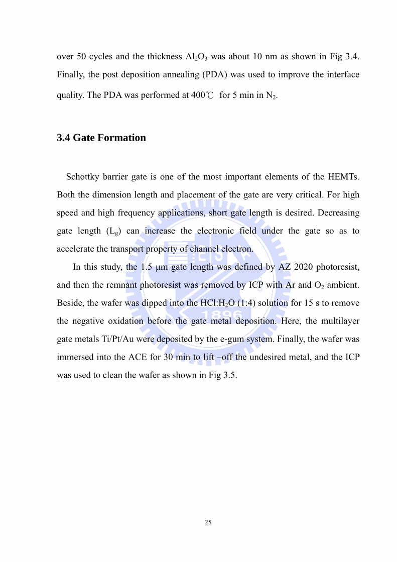

34
width usually mSmm
46 Scattering Parameters [3-2]
Generally the Scattering parameters which referred to as S-parameters are
fundamental to microwave measurement S-parameters are a way of specifying
return loss and insertion loss or insertion gain Fig 45 shows the equivalent
two-port network schematic at high frequency The relation of the microwave
signals and s-parameters are defined as follows
⎥⎦
⎤⎢⎣
⎡⎥⎦
⎤⎢⎣
⎡=⎥
⎦
⎤⎢⎣
⎡
aa
ssss
bb
21
22211211
21 (4-16)
S signals going into or coming out of the input port are labeled by a
subscript 1 Signals going into or coming out of the input port are labeled by a
subscript 2 The electric field of the microwave signal going into the component
ports is designated a that leaving the ports is designated b Therefore
a1 is the electric field of the microwave signal entering the component input
b1 is the electric field of the microwave signal leaving the component input
a2 is the electric field of the microwave signal entering the component output
b2 is the electric field of the microwave signal leaving the component output
By definition then
0211
11=
=aa
bs
0212
21=
=aa
bs
35
0121
12=
=aa
bs
0122
22=
=aa
bs (4-17)
Consequently s11 is the electric field leaving the input divided by the
electric field entering the input under the condition that no signal enters the
output Because b1 and a1 are electric fields their ratio is a reflection coefficient
Similarly s21 is the electric field leaving the output divided by the electric field
entering the input when no signal enters the output Therefore s21 is a
transmission coefficient and is related to the insertion loss or the gain of the
device s22 is similar to s11 but looks in the other direction into the device
47 Current-Gain Cutoff Frequency (fT) and Maximum Oscillation
Frequency ( fmax)
The intrinsic device model for the HEMT device is shown in Fig 46 If we
only consider the intrinsic part the current can be expressed as
2
22
1
21
2
2
12
1
11
1
VyVyi
VyVyi
+=
+= (4-18)
assume (ωCgsRi)2 ltlt 1 then we can get
36
)(
)(
)(
)(
)(
2211
21
1
2
22
21
12
2211
gdgsigs
migsgdm
dsgdd
mgsgdm
gd
gdgsigs
CCjRC
GRCCjG
yy
ii
CCjGy
GCCjGy
Cjy
CCjRCy
++
+minus==
++=
+minus=
minus=
++=
ωω
ω
ω
ω
ω
ωω
(4-19)
assume igsgdgs
migsgdm
RCCC
GRCCG22)(
|)(|
ωω
ω
gtgt+
+gtgt
fT is defined as the frequency when current gain 11
2 =ii and can be
expressed as
)(2 gdgs
mT CC
Gf
+cong
π (4-20)
fmax can be obtained by using unilateral gain
di
T
digs
m
U
GRff
GRCG
f
yyyyGU
141
1)2
(141
)Re()Re(4||
2
2
22
22
11
212
21
max
=
=
minus==
π (4-21)
when U=1 fmax can be expressed as
di
T
GRff
2max = (4-22)
If we further consider gate resistance Rg ohmic contact resistance Rs and Rd
then the small signal equivalent circuit is shown as Fig 47 assume 1)( 2 ltltigs RCω
37
igsgdgs
migsgdm
RCCC
GRCCG22)(
|)(|
ωω
ω
gtgt+
+gtgt
|)(| dsgddm CCjGG ++gtgt ω
then mgd GCjyyyyY ωcongminus= 21
12
22
11
||
Transfer y parameter into Z parameter
sd
s
s
sg
RRYy
Z
RYyZ
RYyZ
RRYyZ
++=
+minus
=
+minus
=
++=
||||
||
||
11
22
21
21
12
12
22
11
and 21122211|| ZZZZZ minus=
mgddgdgssdgdgs
m
mgddsgddgdgssdgdgs
mgddsgddgdgssm
sd
s
GCjGCCjRRCCjG
ii
GCjCCjGCCjRRCCjGCjCCjGCCjRG
YRRyYRy
ZZZ
Z
yy
ii
ωωω
ωωωωωωω
+++++cong
+++++++
+++++minus=
+++minus
===
)]([)()(
)]()][([)()()]()][([
||)(||
||
||
1
2
11
21
22
21
11
21
1
2
)(])(1)[(2 sdmgddsdgdgs
mT RRGCGRRCC
Gf
+++++cong
π (13)
and we can get fmax [28]
2
max
)1)(52
1(54)
1(4 sm
gs
gd
gs
gd
sm
gsim
m
d
T
RGC
CCC
RGRR
RGGG
ff
++++
++
= (14)
fT and fmax are parameters often used to indicate the high frequency
capability of the transistors
38
Fig 41The Transmission Line Method (TLM ) pattern
Fig 42 The illustration of utilizing TLM to measure ohmic contact resistance
39
-30 -25 -20 -15 -10 -5 0 5 10 15-120
-100
-80
-60
-40
-20
0
20
40
60
3rd ORDER PRODUCTS
FUNDAMENTALS
3rd ORDER INTERCEPT POINT
OP1dB
OIP3
O
utpu
t Pow
er (d
Bm
)
Input Power (dBm)
Fig 43 Output power diagram of fundamental andthird-order product signals
Duplexer
AntennafRF
fIF
fLO
LNA Filter Mixer IF amplifier
Signalprocesscircuit
Modulator
PA Pre-amplifier
LO
Fig 44 Fundamental diagram of the microwave front-end device
40
Fig 45 The equivalent two-port network schematic at high frequency
G D
S S
V 1 V 2 g smVG
d sCdG
gsC
gdC
iR
g sV I 2I1
Fig 46 AlGaNGaN HEMT intrinsic device model
G D
S S
gR gdC
gsV1I
1ViR
gsCdsC
dG
dR
2I
gsmVG2V
sR
Fig 47 AlGaNGaN HEMT small signal equivalent circuit
41
Chapter 5
Study of AlGaNGaN MOS-HEMTs on Silicon substrate with
Al2O3 Gate Insulator for Device Linearity Improvement
As shown in chapter 2 device performance of conventional Schottky-gate
AlGaNGaN HEMTs suffers from high gate leakage current Also the drain
current collapses occurs when operating at high bias voltage resulting in poor
long-term reliability of the Schottky gate To improve the leakage characteristics
of the conventional Schottky-gate AlGaNGaN HEMTs devices the fabrication
and characterization of the 15-μm AlGaNGaN MOS-HEMTs with 10 nm Al2O3
high-k gate oxide grown by ALD on Si substrate was investigated Compared to
regular HEMT devices of similar geometry little degradation of the drain
current and gate control ability was observed The result indicates that
AlGaNGaN MOS-HEMTs were the gate leakage currents several orders of
magnitude lower than those of regular HEMTs and exhibit better linearity
higher channel saturation current with improved higher power performance
51 Introduction
Recently with the rapid development of wireless communication system
the transmission speeds of next-generation wireless mobile networks including
Mobile Worldwide Interoperability for Microwave Access (WiMAX) and long
term evolution (LTE) networks will be several tens of megabits per second
Higher speeds will require increased output power leading to increased power
42
consumption by transmission amplifiers so base stations will require
significantly higher power and more physical space Therefore there is a need to
develop compact base stations that offer easy implementation and low operation
costs To make possible a small base station with lower power consumption
high-efficiency power amplifiers are currently being developed using gallium
nitride high electron mobility transistors (GaN-HEMTs) The superior properties
of AlGaNGaN HEMTs promising contenders for high-power high-temperature
high-breakdown and high-frequency applications
However one of the key problems limiting the performance and reliability
of AlGaNGaN HEMTs for high-power RF applications is the high
Schottky-gate leakage current which results in the degradation of DCRF
parameters At positive gate bias high forward gate current can shunt the
gate-channel capacitance thus limiting the maximum drain current At negative
gate bias high voltage drops between the gate and drain resulting in premature
breakdown and the maximum applied drain voltage is restricted Besides gate
leakage current increase resulting in the device sub-threshold currents which
decrease the achievable amplitude of RF output All these limitations become
the most important key factors to be solved for the development of the advanced
wireless communication system
To overcome this problem several groups have been trying to integrate the
MOS structure into conventional Schottky-gate HEMT by looking for proper
gate insulators for AlGaNGaN based HEMT Al2O3 has been used as the gate
insulator to reduce the gate leakage which allows the application of high
positive gate voltage to further increase the sheet electron density in 2D channel
It also offers additional benefits of a wide band gap (about 87eV) high
breakdown electric field (5~20 MVcm) high thermal stability (amorphous up to
43
at least 1000ordmC) and chemical stability compared to AlGaN With
well-controlled thickness and uniform Al2O3 layer deposited by ALD technology
which employs surface saturation reaction technique ALD Al2O3 is the leading
candidate for the gate insulators in MOS-HEMT device
On the other hand in the advanced wireless communication system
multichannel transmissions are extensively used to transmit signals As
transiting signals there are many operating frequencies with the neighboring
frequencies located closely to each other so it is important to consider that the
device used in the communication system would not induce signal distortions
However among all intermodulation distortions third-order intermodulation
distortion (IM3) canrsquot be filtered out by the filter therefore IM3 dominates the
linearity performance of the device and is the most important linearity criteria
for wireless communication system [29] Therefore in this research we study
the linearity characteristics of the Al2O3 AlGaNGaN MOS-HEMTs on Si
substrates and compare it with the regular AlGaNGaN HEMTs devices for
device linearity improvement in this study
52 Device Fabrication
The AlGaNGaN HEMTs structure was grown on Si substrate using
MOCVD technology Electron mobility of 1600 cm2V-1s-1 and sheet carrier
density of 1 1013 cm-2 were measured by hall measurement The device
processing started with ohmic contact formation Ohmic metal TiAlNiAu was
evaporated by e-gun system and then annealed at 800 for 1min in N 2 The
spacing between source and drain is 5μm After Ohmic contact fabrication mesa
44
isolation was attained through dry etch process was controlled by inductive
couple plasma (ICP) with Cl2 in Ar ambient A 10nm amorphous Al2O3 oxide
layer was deposited onto the wafer by atomic layer deposition (ALD) at 300ordmC
prior to the gate formation The ALD technique allows high-quality ultra-thin
material deposition with atomic layer accuracy After gate photolithography a
TiPtAu electrode was evaporated A schematic comparison between HEMT
and MOS-HEMT are fabrication as shown in Fig 51
53 Results and Discussion
Ohmic contact with contact resistance of 28times10-6 (Ohm-cm2) was evaluated
by TLM method Fig 52 shows the typical output current-voltage (I-V)
characteristics of the 15μm gate length AlGaNGaN HEMT and Al2O3
MOS-HEMT The Schottky-gate device has a maximum drain current of 404
mAmm at VGS = 0 while the MOS-HEMT devices have 5442 mAmm drain
currents respectively Besides the HEMTs and MOS-HEMTs were completely
pinch-off at a gate voltage of -5 and -67V respectively The negative shift in the
Vth was attributed to the decrease gate barrier capacitance The experimental Vth
for both HEMTs and MOS-HEMTs were in good agreement with the values
obtained from Eq (5-1) neglecting the residual doping in the AlGaN barrier
layer [6]
sdot=bCs
thenV (5-1)
Where e is the electronic charge ns is the sheet charge density and Cb is the total
unit area capacitance of the barrier layer and dielectric
Fig 53 shows the IDS versus VGS curves of HEMT and MOS-HEMT
devices From a comparison of these device performances it can be seen that the
45
HEMTs have lower IDS of 747 mAmm at VGS = 36 V but for MOS-HEMTs its
reaches 880 mAmm at 6 V gate bias In this sense the good quality of both
Al2O3 insulator and Al2O3HEMT interface has rendered a higher applicable gate
bias which result in a higher driving current capacity of MOS-HEMTs
compared to HEMTs Moreover the drain current at the same gate bias is also
higher for MOS-HEMT This difference arises thereby making the MOS-HEMT
channel depletion for the same gate voltage smaller than that for the HEMT In
Fig 54 a slight transconductance decrease in MOS-HEMTs compared to
HEMTs from 171 to 132 mSmm was observed which is consistent with a
further separation between the control gate and the 2-DEG channel with the
presence of an additional Al2O3 layer in MOS-HEMTs However due to the high
dielectric constant of Al2O3 the degradation in gmmax of MOS-HEMT is only
228 relative to that of HEMT much better than the serve transconductance
deterioration in MOS-HEMTs using low-k gate dielectrics such as SiO2 (272)
Si3N4 (357) This is in agreement with an estimated reduction of 20 by (5-1)
assuming drift velocity saturation (at Lg = 15μm) with Vsat = 5x10⁶ cms In
additional the gate voltage swing (GVS) defined as the 10 drop from the
gmmax increase from 03V for HEMTs to 31 V for MOS-HEMTs The larger
GVS suggests a better linear behavior for MOS-HEMTs compared to
Schottky-gate HEMTs from which a smaller intermodulation distortion a
smaller phase noise and a larger dynamic range could be expected thus
desirable for practical amplifier application
Fig 55 shows the gate leakage performance of the both HEMTs and
MOS-HEMTs with the same device dimensions from which the leakage current
of MOS-HEMTs is found to be significantly lower than that of the Schottky-gate
HEMTs The gate leakage current density of MOS-HEMTs is almost 3 orders of
46
magnitude lower than that of the HEMTs Such a low gate leakage current
should be attributed to the large band offsets in the Al2O3HEMT and a good
quality of both the reactive-sputtered Al2O3 dielectric and the Al2O3HEMT
interface This leads to an increase of the two terminal reverse breakdown
voltage (about 25) and of the forward breakdown voltage (about 30) This
confirms that the Al2O3 dielectric thin film acts as an efficient gate insulator To
investigate the breakdown behavior of Al2O3-insulated gate device the off-state
three-terminal drain-source breakdown characteristics of the HEMT and Al2O3
MOS-HEMT were measured the results are as shown in Fig 56 the devices
were measured at gate voltage Vgs of -8V The breakdown voltage BVDS is
defined as the drain voltage at a gate current of 1mamm which is consistent
with the rapidly increased currents caused by avalanche breakdown The Al2O3
MOS-HEMT with 15μm gate length shows a higher breakdown voltage while
the conventional HEMT The high breakdown voltage is related to the utilization
of the Al2O3 gate insulator to reduce the leakage current
Fig 57 shows IDS vs VGS transfer curves for Al2O3-insulated gate and
Schottky-gate AlGaNGaN HEMTs with the different drain voltages from 4 to 7
V With increasing the drain voltage both of the HEMT and MOS-HEMT
devices have higher maximum drain current except the HEMT at VDS is 7 V In
addition at forward gate bias beyond +2V high drain current drops for the
Schottky-gate HEMT was observed as compare to the MOS-HEMT This is
because the high Schottky-gate leakage current of HEMT with results in the
degradation of the ID On the other hand the slope of ID curve of MOS-HEMT is
lower than regular HEMT however when increasing the gate bias to the
positive voltage the drain current increases at a stable rate in a large gate bias
region This is because Al2O3 gate insulator with larger bandgap that can afford
much higher forward gate bias
47
The characteristics of the Gm dependence on the gate-bias of
Al2O3-insulated and Schottky-gate AlGaNGaN HEMTs with the different drain
voltages from 4 to 7 V are shown in Fig 58 With the increase of the drain
voltage both of the HEMT and MOS-HEMT devices show almost have the
similar maximum transconductance The maximum drain current depends Gm
versus VGS curve the MOS-HEMT device has a lower maximum Gm value but
a flatter Gm distribution as compared to that of regular HEMT It represents that
the drain current increased in a stable rate in a wider range of gate bias region
this may be due to that the gate leakage current was suppressed in the
MOS-HEMT As mentioned before a lower IM3 level can be achieved by
increasing the flatness of the Gm distribution across the gate-bias region in our
current case it indicate that MOS-HEMT may have better device linearity
performance
For linearity assessment nonlinear transfer function based analysis method
is used Previously published results revealed that the Gm were to remain
constant over the operating range of gate bias for minimizing third-order
distortion Hence improving the flatness of the extrinsic Gm profile will result in
lower IM3 levels and higher third-order intercept point (IP3) and thus improve
the device linearity [30] Eq (5-2) shows the relationship between Gm and
drain-source current (IDS) To maintain Gm constant with different gate-source
voltage (VGS) the IDS as a function of VGS should be straight and large
GS
DSdVdI
Gm = (5-2)
To further investigate the linearity performance of the three devices
polynomial curve fitting technique was applied to the transfer characteristic
functions of these devices as equation (5-2)
48
( ) ( ) 5432 45
34
2321 +++++=
partpart
= GSGSGSGSGS
GSDSGSm VaVaVaVaa
VVIVG (5-3)
Hence the relationship between IM3 IP3 and Gm Gds are shown in
equation (5-3) and (5-4) [31-33]
( ) 6
2ds
2
G3 A
RG
IML
m sdotsdot
prop (5-4)
( )Ldsm
m
RGGGIP
sdotsdotprop 2
3
3 (5-5)
In order to improve the device linearity IDS should increase linearly with
VGS Therefore a1 should be larger and the higher order constants while a3 and
a5 should be minimized [34-35] Table 51 shows the coefficients of HEMT and
MOS-HEMT devices It shows that the MOS-HEMT device has higher a1 of
664times10-3 while regular HEMT device has lower a1 of 553times10-3 In addition
the lower a3 is 15646times10-4 and the lower a5 is 433061times10-6 from MOS-HEMT
device From the data analysis the devices linearity improvement can be
achieved by using MOS-HEMT with the Al2O3 as gate insulator approach
To evaluate the device linearity the measurement of IM3 and IP3 of these
devices were necessary The IM3 and IP3 measurements were carried out by
injecting two signals with the same amplitude but at two different frequencies
20 GHz and 2001GHz with the devices biased at VDS = 7V and adjust the IDS to
get the IP3 vs IDS curve Furthermore the load impedance was firstly tuned for
maximum gain in input side and maximum power in output side for each
individual device The measurement results of the IP3 versus IDS curves for these
three different 80nm times 50μm devices are shown in Fig511 It shows that
49
MOS-HEMT devices possess higher IP3 value and wider high IP3 region
versus different IDS The tuning at Γsource and Γload of MOS-HEMT and
HEMT devices were Γsource = 335ang8871ordm and 748ang8947ordm and Γload =
1222ang8662ordm and 1222ang8662ordm respectively From the data in Fig 511 and
Table 51 it can be concluded that Al2O3-insulated gates can achieves flatter Gm
distribution versus VGS bias and thus lower overall IM3 and higher IP3 of these
devices even though Schottky-gate gate device exhibits higher peak Gm
54 Conclusions
The linearity characteristics of the AlGaNGaN HEMT and Al2O3
MOS-HEMT on Si substrates are investigated in this study Although the
MOS-HEMT device demestrated gigher maximum Gm of 132 mSmm at VDS=
7V flatter Gm distribution was achieved for the MOS-HEMT device To further
investigate the linearity performance of the two devices polynomial curve
fitting technique was applied to the transfer characteristic functions It shows
that the MOS-HEMT device has highest a1 and lowest a3 and a5 as compared
with the regular HEMT Therefore the devices linearity improvement can be
achieved by using Al2O3 insulated-gate
The AlGaNGaN HEMTs on Si substrates with Al2O3 gate insulator to
improve the device linearity is demonstrated The reduction of gate leakage
current in MOS-HEMT results in the improvement of the Gm vs VGS curve
flatness and leads to lower overall IM3 and higher IP3 for MOS-HEMT devices
even though the regular HEMT device exhibits higher peak Gm These DC
characteristics lead to higher IP3 levels and lower IM3 for the MOS-HEMT
device as compared to the regular HEMT devices studied The experimental
50
results in this work show that Al2O3 insulated-gate can be practically used on
GaN HEMT devices for the development of high linearity devices for wireless
communication applications
51
(a) (b)
Fig 51 Cross section of the (a) 15μm a Schottky-gate AlGaNGaN HEMT (b)
MOS-HEMT with 10nm Al2O3
52
0 2 4 6 8 10
VGS= +1V to -6V step -1VVGS (V)
Drain-Source Voltage VDS [V]
HEMT
Dra
in c
urre
nt d
ensi
ty I D
S [mA
mm
]
0
100
200
300
400
500
600
700
800
-4V
-3V
-2V
-1V
0V
+1V
-5V
-2V
-1V
0V
+1V
GaN 15um Al2O3 MOS-HEMT and HEMT
MOS-HEMT
Fig 52 DC ID versus VDS characteristics at VGS= 1 to -6 V of the AlGaNGaN
HEMT and Al2O3 MOS-HEMT
53
-8 -6 -4 -2 0 2 4 60
200
400
600
800
1000 HEMT MOS-HEMT
IDmax = 747mmmA VGS=36V
IDmax = 880mmmA VGS=6V
Dra
in c
urre
nt d
ensi
ty I D
S [mA
mm
]
Gate-Source Voltage VGS [V]
Fig 53 IDS versus VGS curve for the AlGaNGaN HEMT and Al2O3
MOS-HEMT at the VDS bias is 7 V
54
-8 -6 -4 -2 0 2 4 6 80
40
80
120
160
200 HEMT MOS-HEMT
Gmmax = 132mmmS VGS=-18V
Gmmax = 171mmmS VGS=-11V
Dra
in c
urre
nt d
ensi
ty I D
S [mA
mm
]
Gate-Source Voltage VGS [V]
Fig 54 Transconductance gm versus gate-source bias VGS at the same drain bias
Vds = 7V in the saturation region for the AlGaNGaN HEMT and Al2O3
MOS-HEMT with gate length =15μm
55
-8 -6 -4 -2 0 2 4 62x10-5
2x10⁻³
2x10⁻¹
2x101
2x10³
VDS= 7V
Gate-Source Voltage VGS [V]
Gat
e cu
rren
t I G
[mA
mm
]
HEMT MOS-HEMT
Fig 55 Gate leakage currents for the AlGaNGaN HEMT and Al2O3
MOS-HEMT with the same device dimensions
56
0 10 20 30 4000
02
04
06
08
10GaN 15um Al2O3 MOS-HEMT
Drain-Source Voltage VDS [V]
ID
IGS
Drain leakage current ID [μA
mm
]Gat
e le
akag
e cu
rren
t Ig [μ
Am
m]
00
02
04
06
08
10
0 10 20 30 40
80
120
160
200
240
280
GaN 15um Regular-HEMT
ID
IGS
Drain-Source Voltage VDS [V]
Drain leakage current ID [μA
mm
]Gat
e le
akag
e cu
rren
t Ig [μ
Am
m]
100120140160180200220240260280
Fig 56 Off-state drain-source breakdown characteristics of Al2O3 MOS-HEMT
and regular-HEMTs
57
-6 -4 -2 0 2 4Dra
in c
urre
nt d
ensi
ty I D
S [mA
mm
]
Gate-Source Voltage VGS [V]
0
200
400
600
800
1000
HEMT MOS-HEMT
VDS= 4V VDS= 5V VDS= 6V VDS= 7V
Fig 57 IDS versus VGS curve for the AlGaNGaN HEMT and Al2O3
MOS-HEMT at the VDS bias is from 4 V to 7 V
58
-6 -4 -2 0 2 4
Tran
scon
duct
ance
GM [m
Sm
m]
Gate-Source Voltage VGS [V]
0
40
80
120
160
200 HEMT MOS-HEMT
VDS= 4V VDS= 5V VDS= 6V VDS= 7V
Fig 58 Gm versus VGS curve for the AlGaNGaN HEMT and Al2O3
MOS-HEMT at the VDS bias is from 4 V to 7 V
59
-4 -2 0 2 4 60
200
400
600
800
GaN 15um MOS-HEMTD
rain
cur
rent
I DS[
mA
mm
]
Gate-Source Voltage VGS [V]
4 V 5 V 6 V 7 V 8 V 9 V 10 V
Fig 59 IDS versus VGS curve for the Al2O3 MOS-HEMT at the VDS bias is from
4 V to 10 V
60
-6 -4 -2 0 2 4 60
20
40
60
80
100
120
140GaN 15um MOS-HEMT
Gate-Source Voltage VGS [V]
Tr
ansc
ondu
ctan
ce G
M [m
Sm
m]
4V 5V 6V 7V 8V 9V 10V
Fig 510 Gm versus VGS curve for the Al2O3 MOS-HEMT at the VDS bias is from
4 V to 10V
61
02 03 04 05 06 07 084
8
12
16
20IP3max = 1893 dBm for MOS-HEMT
Third
ord
er in
terc
ept p
oint
IP3
[dB
m]
Idss []
HEMT MOS-HEMT
Fig 511 IP3 versus IDS curve of the the AlGaNGaN HEMT and Al2O3
MOS-HEMT and the test frequency is 2GHz and VDS =7V
62
Table 51 Comparison of the IP3 of Al2O3 MOS-HEMT and HEMT device at
drain bias is 7V
63
Chapter 6
Conclusion
In this dissertation 15-μm-length Al2O3 AlGaNGaN MOS-HEMTs and
HEMTs grown on Silicon substrate were successfully fabricated and the DC and
RF characteristics were evaluated The maximum IDS of 810 mAmm and peak
extrinsic Gm of 747 mSmm were obtained for the GaN HEMT fabricated
However the AlGaNGaN HEMT suffers from high leakage current In order to
solve this problem an insulated Al2O3 gate was applied to the device to suppress
the high gate leakage current The innovative MOS-HEMT technique not only
reduces the leakage current but also successfully improved the linearity
characteristics of the AlGaNGaN HEMTs on Si substrate It is found that
MOS-HEMT effectively reduced the high electric field in the forward bias it
enables the electrons to maintain a stable electron velocity under the gate
domain and further to suppress high gate leakage current The MOS-HEMT
devices demonstrates increased drain current and maintain stable Gm value under
a larger gate bias domain the MOSHEMTs also demonstrated improvement in
the Gm vs VGS curve flatness and thus leads to lower overall IM3 and higher IP3
for even through the regular HEMT exhibits higher peak Gm For the
MOS-HEMT the maximum third order intermodulation point (IP3) of 1893
dBm was achieved in the MOS-HEMT devices The IP3 was higher them the
regular HEMT device
In addition the third order intermodulation points of the MOS-HEMT and
Schottky-gate device under the different gate biases are also compared in this
study By polynomial curve fitting technique It successfully demonstrate that
64
the multi-gate device have the higher IP3 in the larger IDSS region Therefore
it indicated that multi gate technique could effectively improve the linearity
performance
In conclusion the experimental results in this study shows that in the future
the AlGaNGaN HEMTs with Al3O3-insulated gate have great potential to be
used in the RF power amplifier with improved linearity for the modern wireless
communication system
65
References [1] U K Mishra Linkun Shen T E Kazior and Y-F WuldquoGaN-Based RF
Power Devices and Amplifiersrdquo Proceedings of the IEEE vol 96 no 2
pp287-305 Feb 2008
[2] Y Ando Y Okamoto H Miyamoto T Nakayama T Inoue and M
Kuzuhara ldquo10-Wmm AlGaN-GaN HFET with a field modulating platerdquo IEEE
Electron Device Lett vol 24 no 5 pp 289-291 May 2003
[3] Y F Wu M Moore A Saxler T Wisleder and P Parikh ldquo40 Wmm double
field-plated GaN HEMTsrdquo in Proc Dig Device Res Conf pp 151ndash152 Jun
2006
[4] Y FWu A SaxlerMMoore R P Smith S Sheppard PM Chavarkar
TWisleder U KMishra and P Parikh ldquo30-Wmm GaN HEMTs by field plate
optimizationrdquo IEEE Electron Device Lett vol 25 no 3 pp 117-119 Mar
2004
[5] Y Pei et al ldquoRecessed Slant Gate AlGaNGaN High Electron Mobility
Transistors with 209Wmm at 10GHz rdquo Jpn J Appl Phys Vol 46pp
L1087-L10892007
[6] Wu YQ Y Xuan T Shen PD Ye Z Cheng and A Lochtefeld
Enhancement-mode InP n-channel metal-oxide-semiconductor field-effect
transistors with atomic-layer-deposited Al2O3 dielectrics Appl Phys Lett vol
91 no 2 2007
[7] Huang ML YC Chang CH Chang YJ Lee P Chang J Kwo TB
Wu and M Hong Surface passivation of III-V compound semiconductors
using atomic-layer-deposition-grown Al2O3 Appl Phys Lett vol 87 no 25
2005
66
[8] Xuan Y HC Lin PD Ye and GD Wilk Capacitance-voltage studies
on enhancement-mode InGaAs metal-oxide-semiconductor field-effect transistor
using atomic-layer-deposited Al2O3 gate dielectric Appl Phys Lett vol 88
no 26 2006
[9] O Ambachera) J Smart J R Shealy N G Weimann K Chu M
MurphyW J Schaff and L F Eastmanrdquo Two-dimensional electron gases
induced by spontaneous and piezoelectric polarization charges in N- and
Ga-face AlGaNGaN heterostructuresrdquo Journal of Applied Physics vol 85 no
6 15 1999
[10] S Nakamura GaN Growth Using GaN Buffer Layer Jpn J Appl Phys
vol 30 pp L1705-L1707 1991
[11] D Kapolnek et al Structural evolution in epitaxial metalorganic chemical
vapor deposition grown GaN films on sapphire Appl Phys Lett vol 67 pp
1541-1543 1995
[12] L Zhou et al Effect of AlN flux ratio during nucleation layer growth on
the microstructure of GaN films grown by molecular-beam epitaxy Appl Phys
Lett vol 88 p 011916 2006
[13] J C Zhang et al The influence of AlN buffer layer thickness on the
properties of GaN epilayer J Crys Growth vol 268 pp 24-29 2004
[14] D G Zhao et al Surface morphology of AlN buffer layer and its effect
on GaN growth by metalorganic chemical vapor deposition Appl Phys Lett
vol 85 pp 1499-1501 2004
[15] L Meshi et al The reduction of threading dislocations in GaN using a
GaN nanocolumn interlayer Phys Status Solidi (c) vol 5 pp 1645-1647
2008
[16] M J Manfra et al Dislocation and morphology control during
67
molecular-beam epitaxy of AlGaNGaN heterostructures directly on sapphire
substrates Appl Phys Lett vol 81 pp 1456-1458 2002
[17] K Uchida et al Characterization of Double-Buffer Layers and Its
Application for the Metalorganic Vapor Phase Epitaxial Growth of GaN Jpn J
Appl Phys vol 37 pp 3882-3888 1998
[18] L K Li et al High electron mobility AlGaNGaN heterostructures grown
on sapphire substrates by molecular-beam epitaxy Appl Phys Lett vol 76 pp
742-744 2000
[19] Y B Pan et al Reduction of threading edge dislocation density in n-type
GaN by Si delta-doping J Crys Growth vol 286 pp 255-258 2006
[20] A Corrion et al Review of Recent Developments in Growth of
AlGaNGaN High-Electron Mobility Transistors on 4H-SiC by Plasma-Assisted
Molecular Beam Epitaxy IEICE Trans Electron vol E89-C pp 906-912 2006
[21] J P Ibbetson et al Polarization effects surface states and the source of
electrons in AlGaNGaN heterostructure field effect transistors Appl Phys
Lett vol 77 pp 250-252 2000
[22] M Miyoshi et al ldquoMetalorganic Chemical Vapor Deposition and Material
Characterization of Lattice-Matched InAlNGaN Two-Dimensional Electron
Gas Heterostructuresrdquo Appl Phys Express vol 1 p 081102 2008
[23] A Chini et al ldquo21 Amm current density AlGaNGaN HEMTrdquo Electron
Lett vol 39 pp 625-626 2003
[24] S L Rumyantsev N Pala M S Shur ME Levinshtein R GaskaM Asif
Khan and G Simin Generation-Recombination Noise in GaN-based Devices
in GaN-based materials and devices Selected topics in electronics and
systems - v33 eds MSShur and RF Devis World Scientific 2004 ISBN
981-238-844-3
68
[25] EJ Miller XZ Dang HH Wieder PH Asbeck ETYu GJ Sullivan
and JM Redwing ldquoTrap characterization by gate-drain conductance and
capacitance dispersion studies of an AlGaNGaN heterostructure field-effect
transistorrdquo Jpn J Appl vol 87 8070 2000
[26] Shinya MIZUNO Yutaka OHNO Shigeru KISHIMOTO Koichi
MAEZAWA and Takashi MIZUTANI Jpn J Appl Phys vol 41 no 8 pp
5125-5126 Part 1 August 2002
[27]Kim HS I Ok M Zhang F Zhu S Park J Yum H Zhao JC Lee P
Majhi N Goel W Tsai CK Gaspe and MB Santos A study of
metal-oxide-semiconductor capacitors on GaAs In053Ga047As InAs and InSb
substrates using a germanium interfacial passivation layer Appl Phys Lett
93(6)(2008)
[28] Ok I H Kim M Zhang F Zhu S Park J Yum H Zhao D Garcia P
Majhi N Goel W Tsai CK Gaspe MB Santos and JC Lee Self-aligned
n-channel metal-oxide-semiconductor field effect transistor on
high-indium-content In053Ga047As and InP using physical vapor deposition
HfO2 and silicon interface passivation layer Appl Phys Lett 92(20)(2008)
[29] Zhao H HS Kim F Zhu M Zhang I Ok SI Park JH Yum and JC
Lee Metal-oxide-semiconductor capacitors on GaAs with germanium nitride
passivation layer Appl Phys Lett 91(17) (2007)
[30] Oktyabrsky S V Tokranov M Yakimov R Moore S Koveshnikov W
Tsai F Zhu and JC Lee High-k gate stack on GaAs and InGaAs using in situ
passivation with amorphous silicon Mater Sci Eng B-Solid State Mater Adv
Technol 135(3) P272-276 (2006)
[31] Zhao H JH Yum YT Chen and JC Lee In053Ga047As
n-metal-oxide-semiconductor field effect transistors with atomic layer deposited
69
Al2O3 HfO2 and LaAlO3 gate dielectrics J Vac Sci Technol B 27(4)
P2024-2027 (2009)
[32] Xuan Y YQ Wu T Shen T Yang and PD Ye High performance
submicron inversion-type enhancement-mode InGaAs MOSFETs with ALD
Al2O3 HfO2 and HfAlO as gate dielectrics IEEE New York Vols 1 and 2
p637-640 (2007)
[33] OConnor E RD Long K Cherkaoui KK Thomas F Chalvet IM
Povey ME Pemble PK Hurley B Brennan G Hughes and SB Newcomb
In situ H2S passivation of In053Ga047AsInP metal-oxide-semiconductor
capacitors with atomic-layer deposited HfO2 gate dielectric Appl Phys Lett
92(2)(2008)
[34] S M SZE Semiconductor devices physics and technology 2nd edition
Wiley (2002)
[35] T Ytterdal Y Cheng and T A Fjeldly Devices Modeling for analog and
RF CMOS Circuit Design John Wiley and Sons(2003)
Devices 55(2) P547-556 (2008)
Wiley(2007)

40
Fig 45 The equivalent two-port network schematic at high frequency
G D
S S
V 1 V 2 g smVG
d sCdG
gsC
gdC
iR
g sV I 2I1
Fig 46 AlGaNGaN HEMT intrinsic device model
G D
S S
gR gdC
gsV1I
1ViR
gsCdsC
dG
dR
2I
gsmVG2V
sR
Fig 47 AlGaNGaN HEMT small signal equivalent circuit
41
Chapter 5
Study of AlGaNGaN MOS-HEMTs on Silicon substrate with
Al2O3 Gate Insulator for Device Linearity Improvement
As shown in chapter 2 device performance of conventional Schottky-gate
AlGaNGaN HEMTs suffers from high gate leakage current Also the drain
current collapses occurs when operating at high bias voltage resulting in poor
long-term reliability of the Schottky gate To improve the leakage characteristics
of the conventional Schottky-gate AlGaNGaN HEMTs devices the fabrication
and characterization of the 15-μm AlGaNGaN MOS-HEMTs with 10 nm Al2O3
high-k gate oxide grown by ALD on Si substrate was investigated Compared to
regular HEMT devices of similar geometry little degradation of the drain
current and gate control ability was observed The result indicates that
AlGaNGaN MOS-HEMTs were the gate leakage currents several orders of
magnitude lower than those of regular HEMTs and exhibit better linearity
higher channel saturation current with improved higher power performance
51 Introduction
Recently with the rapid development of wireless communication system
the transmission speeds of next-generation wireless mobile networks including
Mobile Worldwide Interoperability for Microwave Access (WiMAX) and long
term evolution (LTE) networks will be several tens of megabits per second
Higher speeds will require increased output power leading to increased power
42
consumption by transmission amplifiers so base stations will require
significantly higher power and more physical space Therefore there is a need to
develop compact base stations that offer easy implementation and low operation
costs To make possible a small base station with lower power consumption
high-efficiency power amplifiers are currently being developed using gallium
nitride high electron mobility transistors (GaN-HEMTs) The superior properties
of AlGaNGaN HEMTs promising contenders for high-power high-temperature
high-breakdown and high-frequency applications
However one of the key problems limiting the performance and reliability
of AlGaNGaN HEMTs for high-power RF applications is the high
Schottky-gate leakage current which results in the degradation of DCRF
parameters At positive gate bias high forward gate current can shunt the
gate-channel capacitance thus limiting the maximum drain current At negative
gate bias high voltage drops between the gate and drain resulting in premature
breakdown and the maximum applied drain voltage is restricted Besides gate
leakage current increase resulting in the device sub-threshold currents which
decrease the achievable amplitude of RF output All these limitations become
the most important key factors to be solved for the development of the advanced
wireless communication system
To overcome this problem several groups have been trying to integrate the
MOS structure into conventional Schottky-gate HEMT by looking for proper
gate insulators for AlGaNGaN based HEMT Al2O3 has been used as the gate
insulator to reduce the gate leakage which allows the application of high
positive gate voltage to further increase the sheet electron density in 2D channel
It also offers additional benefits of a wide band gap (about 87eV) high
breakdown electric field (5~20 MVcm) high thermal stability (amorphous up to
43
at least 1000ordmC) and chemical stability compared to AlGaN With
well-controlled thickness and uniform Al2O3 layer deposited by ALD technology
which employs surface saturation reaction technique ALD Al2O3 is the leading
candidate for the gate insulators in MOS-HEMT device
On the other hand in the advanced wireless communication system
multichannel transmissions are extensively used to transmit signals As
transiting signals there are many operating frequencies with the neighboring
frequencies located closely to each other so it is important to consider that the
device used in the communication system would not induce signal distortions
However among all intermodulation distortions third-order intermodulation
distortion (IM3) canrsquot be filtered out by the filter therefore IM3 dominates the
linearity performance of the device and is the most important linearity criteria
for wireless communication system [29] Therefore in this research we study
the linearity characteristics of the Al2O3 AlGaNGaN MOS-HEMTs on Si
substrates and compare it with the regular AlGaNGaN HEMTs devices for
device linearity improvement in this study
52 Device Fabrication
The AlGaNGaN HEMTs structure was grown on Si substrate using
MOCVD technology Electron mobility of 1600 cm2V-1s-1 and sheet carrier
density of 1 1013 cm-2 were measured by hall measurement The device
processing started with ohmic contact formation Ohmic metal TiAlNiAu was
evaporated by e-gun system and then annealed at 800 for 1min in N 2 The
spacing between source and drain is 5μm After Ohmic contact fabrication mesa
44
isolation was attained through dry etch process was controlled by inductive
couple plasma (ICP) with Cl2 in Ar ambient A 10nm amorphous Al2O3 oxide
layer was deposited onto the wafer by atomic layer deposition (ALD) at 300ordmC
prior to the gate formation The ALD technique allows high-quality ultra-thin
material deposition with atomic layer accuracy After gate photolithography a
TiPtAu electrode was evaporated A schematic comparison between HEMT
and MOS-HEMT are fabrication as shown in Fig 51
53 Results and Discussion
Ohmic contact with contact resistance of 28times10-6 (Ohm-cm2) was evaluated
by TLM method Fig 52 shows the typical output current-voltage (I-V)
characteristics of the 15μm gate length AlGaNGaN HEMT and Al2O3
MOS-HEMT The Schottky-gate device has a maximum drain current of 404
mAmm at VGS = 0 while the MOS-HEMT devices have 5442 mAmm drain
currents respectively Besides the HEMTs and MOS-HEMTs were completely
pinch-off at a gate voltage of -5 and -67V respectively The negative shift in the
Vth was attributed to the decrease gate barrier capacitance The experimental Vth
for both HEMTs and MOS-HEMTs were in good agreement with the values
obtained from Eq (5-1) neglecting the residual doping in the AlGaN barrier
layer [6]
sdot=bCs
thenV (5-1)
Where e is the electronic charge ns is the sheet charge density and Cb is the total
unit area capacitance of the barrier layer and dielectric
Fig 53 shows the IDS versus VGS curves of HEMT and MOS-HEMT
devices From a comparison of these device performances it can be seen that the
45
HEMTs have lower IDS of 747 mAmm at VGS = 36 V but for MOS-HEMTs its
reaches 880 mAmm at 6 V gate bias In this sense the good quality of both
Al2O3 insulator and Al2O3HEMT interface has rendered a higher applicable gate
bias which result in a higher driving current capacity of MOS-HEMTs
compared to HEMTs Moreover the drain current at the same gate bias is also
higher for MOS-HEMT This difference arises thereby making the MOS-HEMT
channel depletion for the same gate voltage smaller than that for the HEMT In
Fig 54 a slight transconductance decrease in MOS-HEMTs compared to
HEMTs from 171 to 132 mSmm was observed which is consistent with a
further separation between the control gate and the 2-DEG channel with the
presence of an additional Al2O3 layer in MOS-HEMTs However due to the high
dielectric constant of Al2O3 the degradation in gmmax of MOS-HEMT is only
228 relative to that of HEMT much better than the serve transconductance
deterioration in MOS-HEMTs using low-k gate dielectrics such as SiO2 (272)
Si3N4 (357) This is in agreement with an estimated reduction of 20 by (5-1)
assuming drift velocity saturation (at Lg = 15μm) with Vsat = 5x10⁶ cms In
additional the gate voltage swing (GVS) defined as the 10 drop from the
gmmax increase from 03V for HEMTs to 31 V for MOS-HEMTs The larger
GVS suggests a better linear behavior for MOS-HEMTs compared to
Schottky-gate HEMTs from which a smaller intermodulation distortion a
smaller phase noise and a larger dynamic range could be expected thus
desirable for practical amplifier application
Fig 55 shows the gate leakage performance of the both HEMTs and
MOS-HEMTs with the same device dimensions from which the leakage current
of MOS-HEMTs is found to be significantly lower than that of the Schottky-gate
HEMTs The gate leakage current density of MOS-HEMTs is almost 3 orders of
46
magnitude lower than that of the HEMTs Such a low gate leakage current
should be attributed to the large band offsets in the Al2O3HEMT and a good
quality of both the reactive-sputtered Al2O3 dielectric and the Al2O3HEMT
interface This leads to an increase of the two terminal reverse breakdown
voltage (about 25) and of the forward breakdown voltage (about 30) This
confirms that the Al2O3 dielectric thin film acts as an efficient gate insulator To
investigate the breakdown behavior of Al2O3-insulated gate device the off-state
three-terminal drain-source breakdown characteristics of the HEMT and Al2O3
MOS-HEMT were measured the results are as shown in Fig 56 the devices
were measured at gate voltage Vgs of -8V The breakdown voltage BVDS is
defined as the drain voltage at a gate current of 1mamm which is consistent
with the rapidly increased currents caused by avalanche breakdown The Al2O3
MOS-HEMT with 15μm gate length shows a higher breakdown voltage while
the conventional HEMT The high breakdown voltage is related to the utilization
of the Al2O3 gate insulator to reduce the leakage current
Fig 57 shows IDS vs VGS transfer curves for Al2O3-insulated gate and
Schottky-gate AlGaNGaN HEMTs with the different drain voltages from 4 to 7
V With increasing the drain voltage both of the HEMT and MOS-HEMT
devices have higher maximum drain current except the HEMT at VDS is 7 V In
addition at forward gate bias beyond +2V high drain current drops for the
Schottky-gate HEMT was observed as compare to the MOS-HEMT This is
because the high Schottky-gate leakage current of HEMT with results in the
degradation of the ID On the other hand the slope of ID curve of MOS-HEMT is
lower than regular HEMT however when increasing the gate bias to the
positive voltage the drain current increases at a stable rate in a large gate bias
region This is because Al2O3 gate insulator with larger bandgap that can afford
much higher forward gate bias
47
The characteristics of the Gm dependence on the gate-bias of
Al2O3-insulated and Schottky-gate AlGaNGaN HEMTs with the different drain
voltages from 4 to 7 V are shown in Fig 58 With the increase of the drain
voltage both of the HEMT and MOS-HEMT devices show almost have the
similar maximum transconductance The maximum drain current depends Gm
versus VGS curve the MOS-HEMT device has a lower maximum Gm value but
a flatter Gm distribution as compared to that of regular HEMT It represents that
the drain current increased in a stable rate in a wider range of gate bias region
this may be due to that the gate leakage current was suppressed in the
MOS-HEMT As mentioned before a lower IM3 level can be achieved by
increasing the flatness of the Gm distribution across the gate-bias region in our
current case it indicate that MOS-HEMT may have better device linearity
performance
For linearity assessment nonlinear transfer function based analysis method
is used Previously published results revealed that the Gm were to remain
constant over the operating range of gate bias for minimizing third-order
distortion Hence improving the flatness of the extrinsic Gm profile will result in
lower IM3 levels and higher third-order intercept point (IP3) and thus improve
the device linearity [30] Eq (5-2) shows the relationship between Gm and
drain-source current (IDS) To maintain Gm constant with different gate-source
voltage (VGS) the IDS as a function of VGS should be straight and large
GS
DSdVdI
Gm = (5-2)
To further investigate the linearity performance of the three devices
polynomial curve fitting technique was applied to the transfer characteristic
functions of these devices as equation (5-2)
48
( ) ( ) 5432 45
34
2321 +++++=
partpart
= GSGSGSGSGS
GSDSGSm VaVaVaVaa
VVIVG (5-3)
Hence the relationship between IM3 IP3 and Gm Gds are shown in
equation (5-3) and (5-4) [31-33]
( ) 6
2ds
2
G3 A
RG
IML
m sdotsdot
prop (5-4)
( )Ldsm
m
RGGGIP
sdotsdotprop 2
3
3 (5-5)
In order to improve the device linearity IDS should increase linearly with
VGS Therefore a1 should be larger and the higher order constants while a3 and
a5 should be minimized [34-35] Table 51 shows the coefficients of HEMT and
MOS-HEMT devices It shows that the MOS-HEMT device has higher a1 of
664times10-3 while regular HEMT device has lower a1 of 553times10-3 In addition
the lower a3 is 15646times10-4 and the lower a5 is 433061times10-6 from MOS-HEMT
device From the data analysis the devices linearity improvement can be
achieved by using MOS-HEMT with the Al2O3 as gate insulator approach
To evaluate the device linearity the measurement of IM3 and IP3 of these
devices were necessary The IM3 and IP3 measurements were carried out by
injecting two signals with the same amplitude but at two different frequencies
20 GHz and 2001GHz with the devices biased at VDS = 7V and adjust the IDS to
get the IP3 vs IDS curve Furthermore the load impedance was firstly tuned for
maximum gain in input side and maximum power in output side for each
individual device The measurement results of the IP3 versus IDS curves for these
three different 80nm times 50μm devices are shown in Fig511 It shows that
49
MOS-HEMT devices possess higher IP3 value and wider high IP3 region
versus different IDS The tuning at Γsource and Γload of MOS-HEMT and
HEMT devices were Γsource = 335ang8871ordm and 748ang8947ordm and Γload =
1222ang8662ordm and 1222ang8662ordm respectively From the data in Fig 511 and
Table 51 it can be concluded that Al2O3-insulated gates can achieves flatter Gm
distribution versus VGS bias and thus lower overall IM3 and higher IP3 of these
devices even though Schottky-gate gate device exhibits higher peak Gm
54 Conclusions
The linearity characteristics of the AlGaNGaN HEMT and Al2O3
MOS-HEMT on Si substrates are investigated in this study Although the
MOS-HEMT device demestrated gigher maximum Gm of 132 mSmm at VDS=
7V flatter Gm distribution was achieved for the MOS-HEMT device To further
investigate the linearity performance of the two devices polynomial curve
fitting technique was applied to the transfer characteristic functions It shows
that the MOS-HEMT device has highest a1 and lowest a3 and a5 as compared
with the regular HEMT Therefore the devices linearity improvement can be
achieved by using Al2O3 insulated-gate
The AlGaNGaN HEMTs on Si substrates with Al2O3 gate insulator to
improve the device linearity is demonstrated The reduction of gate leakage
current in MOS-HEMT results in the improvement of the Gm vs VGS curve
flatness and leads to lower overall IM3 and higher IP3 for MOS-HEMT devices
even though the regular HEMT device exhibits higher peak Gm These DC
characteristics lead to higher IP3 levels and lower IM3 for the MOS-HEMT
device as compared to the regular HEMT devices studied The experimental
50
results in this work show that Al2O3 insulated-gate can be practically used on
GaN HEMT devices for the development of high linearity devices for wireless
communication applications
51
(a) (b)
Fig 51 Cross section of the (a) 15μm a Schottky-gate AlGaNGaN HEMT (b)
MOS-HEMT with 10nm Al2O3
52
0 2 4 6 8 10
VGS= +1V to -6V step -1VVGS (V)
Drain-Source Voltage VDS [V]
HEMT
Dra
in c
urre
nt d
ensi
ty I D
S [mA
mm
]
0
100
200
300
400
500
600
700
800
-4V
-3V
-2V
-1V
0V
+1V
-5V
-2V
-1V
0V
+1V
GaN 15um Al2O3 MOS-HEMT and HEMT
MOS-HEMT
Fig 52 DC ID versus VDS characteristics at VGS= 1 to -6 V of the AlGaNGaN
HEMT and Al2O3 MOS-HEMT
53
-8 -6 -4 -2 0 2 4 60
200
400
600
800
1000 HEMT MOS-HEMT
IDmax = 747mmmA VGS=36V
IDmax = 880mmmA VGS=6V
Dra
in c
urre
nt d
ensi
ty I D
S [mA
mm
]
Gate-Source Voltage VGS [V]
Fig 53 IDS versus VGS curve for the AlGaNGaN HEMT and Al2O3
MOS-HEMT at the VDS bias is 7 V
54
-8 -6 -4 -2 0 2 4 6 80
40
80
120
160
200 HEMT MOS-HEMT
Gmmax = 132mmmS VGS=-18V
Gmmax = 171mmmS VGS=-11V
Dra
in c
urre
nt d
ensi
ty I D
S [mA
mm
]
Gate-Source Voltage VGS [V]
Fig 54 Transconductance gm versus gate-source bias VGS at the same drain bias
Vds = 7V in the saturation region for the AlGaNGaN HEMT and Al2O3
MOS-HEMT with gate length =15μm
55
-8 -6 -4 -2 0 2 4 62x10-5
2x10⁻³
2x10⁻¹
2x101
2x10³
VDS= 7V
Gate-Source Voltage VGS [V]
Gat
e cu
rren
t I G
[mA
mm
]
HEMT MOS-HEMT
Fig 55 Gate leakage currents for the AlGaNGaN HEMT and Al2O3
MOS-HEMT with the same device dimensions
56
0 10 20 30 4000
02
04
06
08
10GaN 15um Al2O3 MOS-HEMT
Drain-Source Voltage VDS [V]
ID
IGS
Drain leakage current ID [μA
mm
]Gat
e le
akag
e cu
rren
t Ig [μ
Am
m]
00
02
04
06
08
10
0 10 20 30 40
80
120
160
200
240
280
GaN 15um Regular-HEMT
ID
IGS
Drain-Source Voltage VDS [V]
Drain leakage current ID [μA
mm
]Gat
e le
akag
e cu
rren
t Ig [μ
Am
m]
100120140160180200220240260280
Fig 56 Off-state drain-source breakdown characteristics of Al2O3 MOS-HEMT
and regular-HEMTs
57
-6 -4 -2 0 2 4Dra
in c
urre
nt d
ensi
ty I D
S [mA
mm
]
Gate-Source Voltage VGS [V]
0
200
400
600
800
1000
HEMT MOS-HEMT
VDS= 4V VDS= 5V VDS= 6V VDS= 7V
Fig 57 IDS versus VGS curve for the AlGaNGaN HEMT and Al2O3
MOS-HEMT at the VDS bias is from 4 V to 7 V
58
-6 -4 -2 0 2 4
Tran
scon
duct
ance
GM [m
Sm
m]
Gate-Source Voltage VGS [V]
0
40
80
120
160
200 HEMT MOS-HEMT
VDS= 4V VDS= 5V VDS= 6V VDS= 7V
Fig 58 Gm versus VGS curve for the AlGaNGaN HEMT and Al2O3
MOS-HEMT at the VDS bias is from 4 V to 7 V
59
-4 -2 0 2 4 60
200
400
600
800
GaN 15um MOS-HEMTD
rain
cur
rent
I DS[
mA
mm
]
Gate-Source Voltage VGS [V]
4 V 5 V 6 V 7 V 8 V 9 V 10 V
Fig 59 IDS versus VGS curve for the Al2O3 MOS-HEMT at the VDS bias is from
4 V to 10 V
60
-6 -4 -2 0 2 4 60
20
40
60
80
100
120
140GaN 15um MOS-HEMT
Gate-Source Voltage VGS [V]
Tr
ansc
ondu
ctan
ce G
M [m
Sm
m]
4V 5V 6V 7V 8V 9V 10V
Fig 510 Gm versus VGS curve for the Al2O3 MOS-HEMT at the VDS bias is from
4 V to 10V
61
02 03 04 05 06 07 084
8
12
16
20IP3max = 1893 dBm for MOS-HEMT
Third
ord
er in
terc
ept p
oint
IP3
[dB
m]
Idss []
HEMT MOS-HEMT
Fig 511 IP3 versus IDS curve of the the AlGaNGaN HEMT and Al2O3
MOS-HEMT and the test frequency is 2GHz and VDS =7V
62
Table 51 Comparison of the IP3 of Al2O3 MOS-HEMT and HEMT device at
drain bias is 7V
63
Chapter 6
Conclusion
In this dissertation 15-μm-length Al2O3 AlGaNGaN MOS-HEMTs and
HEMTs grown on Silicon substrate were successfully fabricated and the DC and
RF characteristics were evaluated The maximum IDS of 810 mAmm and peak
extrinsic Gm of 747 mSmm were obtained for the GaN HEMT fabricated
However the AlGaNGaN HEMT suffers from high leakage current In order to
solve this problem an insulated Al2O3 gate was applied to the device to suppress
the high gate leakage current The innovative MOS-HEMT technique not only
reduces the leakage current but also successfully improved the linearity
characteristics of the AlGaNGaN HEMTs on Si substrate It is found that
MOS-HEMT effectively reduced the high electric field in the forward bias it
enables the electrons to maintain a stable electron velocity under the gate
domain and further to suppress high gate leakage current The MOS-HEMT
devices demonstrates increased drain current and maintain stable Gm value under
a larger gate bias domain the MOSHEMTs also demonstrated improvement in
the Gm vs VGS curve flatness and thus leads to lower overall IM3 and higher IP3
for even through the regular HEMT exhibits higher peak Gm For the
MOS-HEMT the maximum third order intermodulation point (IP3) of 1893
dBm was achieved in the MOS-HEMT devices The IP3 was higher them the
regular HEMT device
In addition the third order intermodulation points of the MOS-HEMT and
Schottky-gate device under the different gate biases are also compared in this
study By polynomial curve fitting technique It successfully demonstrate that
64
the multi-gate device have the higher IP3 in the larger IDSS region Therefore
it indicated that multi gate technique could effectively improve the linearity
performance
In conclusion the experimental results in this study shows that in the future
the AlGaNGaN HEMTs with Al3O3-insulated gate have great potential to be
used in the RF power amplifier with improved linearity for the modern wireless
communication system
65
References [1] U K Mishra Linkun Shen T E Kazior and Y-F WuldquoGaN-Based RF
Power Devices and Amplifiersrdquo Proceedings of the IEEE vol 96 no 2
pp287-305 Feb 2008
[2] Y Ando Y Okamoto H Miyamoto T Nakayama T Inoue and M
Kuzuhara ldquo10-Wmm AlGaN-GaN HFET with a field modulating platerdquo IEEE
Electron Device Lett vol 24 no 5 pp 289-291 May 2003
[3] Y F Wu M Moore A Saxler T Wisleder and P Parikh ldquo40 Wmm double
field-plated GaN HEMTsrdquo in Proc Dig Device Res Conf pp 151ndash152 Jun
2006
[4] Y FWu A SaxlerMMoore R P Smith S Sheppard PM Chavarkar
TWisleder U KMishra and P Parikh ldquo30-Wmm GaN HEMTs by field plate
optimizationrdquo IEEE Electron Device Lett vol 25 no 3 pp 117-119 Mar
2004
[5] Y Pei et al ldquoRecessed Slant Gate AlGaNGaN High Electron Mobility
Transistors with 209Wmm at 10GHz rdquo Jpn J Appl Phys Vol 46pp
L1087-L10892007
[6] Wu YQ Y Xuan T Shen PD Ye Z Cheng and A Lochtefeld
Enhancement-mode InP n-channel metal-oxide-semiconductor field-effect
transistors with atomic-layer-deposited Al2O3 dielectrics Appl Phys Lett vol
91 no 2 2007
[7] Huang ML YC Chang CH Chang YJ Lee P Chang J Kwo TB
Wu and M Hong Surface passivation of III-V compound semiconductors
using atomic-layer-deposition-grown Al2O3 Appl Phys Lett vol 87 no 25
2005
66
[8] Xuan Y HC Lin PD Ye and GD Wilk Capacitance-voltage studies
on enhancement-mode InGaAs metal-oxide-semiconductor field-effect transistor
using atomic-layer-deposited Al2O3 gate dielectric Appl Phys Lett vol 88
no 26 2006
[9] O Ambachera) J Smart J R Shealy N G Weimann K Chu M
MurphyW J Schaff and L F Eastmanrdquo Two-dimensional electron gases
induced by spontaneous and piezoelectric polarization charges in N- and
Ga-face AlGaNGaN heterostructuresrdquo Journal of Applied Physics vol 85 no
6 15 1999
[10] S Nakamura GaN Growth Using GaN Buffer Layer Jpn J Appl Phys
vol 30 pp L1705-L1707 1991
[11] D Kapolnek et al Structural evolution in epitaxial metalorganic chemical
vapor deposition grown GaN films on sapphire Appl Phys Lett vol 67 pp
1541-1543 1995
[12] L Zhou et al Effect of AlN flux ratio during nucleation layer growth on
the microstructure of GaN films grown by molecular-beam epitaxy Appl Phys
Lett vol 88 p 011916 2006
[13] J C Zhang et al The influence of AlN buffer layer thickness on the
properties of GaN epilayer J Crys Growth vol 268 pp 24-29 2004
[14] D G Zhao et al Surface morphology of AlN buffer layer and its effect
on GaN growth by metalorganic chemical vapor deposition Appl Phys Lett
vol 85 pp 1499-1501 2004
[15] L Meshi et al The reduction of threading dislocations in GaN using a
GaN nanocolumn interlayer Phys Status Solidi (c) vol 5 pp 1645-1647
2008
[16] M J Manfra et al Dislocation and morphology control during
67
molecular-beam epitaxy of AlGaNGaN heterostructures directly on sapphire
substrates Appl Phys Lett vol 81 pp 1456-1458 2002
[17] K Uchida et al Characterization of Double-Buffer Layers and Its
Application for the Metalorganic Vapor Phase Epitaxial Growth of GaN Jpn J
Appl Phys vol 37 pp 3882-3888 1998
[18] L K Li et al High electron mobility AlGaNGaN heterostructures grown
on sapphire substrates by molecular-beam epitaxy Appl Phys Lett vol 76 pp
742-744 2000
[19] Y B Pan et al Reduction of threading edge dislocation density in n-type
GaN by Si delta-doping J Crys Growth vol 286 pp 255-258 2006
[20] A Corrion et al Review of Recent Developments in Growth of
AlGaNGaN High-Electron Mobility Transistors on 4H-SiC by Plasma-Assisted
Molecular Beam Epitaxy IEICE Trans Electron vol E89-C pp 906-912 2006
[21] J P Ibbetson et al Polarization effects surface states and the source of
electrons in AlGaNGaN heterostructure field effect transistors Appl Phys
Lett vol 77 pp 250-252 2000
[22] M Miyoshi et al ldquoMetalorganic Chemical Vapor Deposition and Material
Characterization of Lattice-Matched InAlNGaN Two-Dimensional Electron
Gas Heterostructuresrdquo Appl Phys Express vol 1 p 081102 2008
[23] A Chini et al ldquo21 Amm current density AlGaNGaN HEMTrdquo Electron
Lett vol 39 pp 625-626 2003
[24] S L Rumyantsev N Pala M S Shur ME Levinshtein R GaskaM Asif
Khan and G Simin Generation-Recombination Noise in GaN-based Devices
in GaN-based materials and devices Selected topics in electronics and
systems - v33 eds MSShur and RF Devis World Scientific 2004 ISBN
981-238-844-3
68
[25] EJ Miller XZ Dang HH Wieder PH Asbeck ETYu GJ Sullivan
and JM Redwing ldquoTrap characterization by gate-drain conductance and
capacitance dispersion studies of an AlGaNGaN heterostructure field-effect
transistorrdquo Jpn J Appl vol 87 8070 2000
[26] Shinya MIZUNO Yutaka OHNO Shigeru KISHIMOTO Koichi
MAEZAWA and Takashi MIZUTANI Jpn J Appl Phys vol 41 no 8 pp
5125-5126 Part 1 August 2002
[27]Kim HS I Ok M Zhang F Zhu S Park J Yum H Zhao JC Lee P
Majhi N Goel W Tsai CK Gaspe and MB Santos A study of
metal-oxide-semiconductor capacitors on GaAs In053Ga047As InAs and InSb
substrates using a germanium interfacial passivation layer Appl Phys Lett
93(6)(2008)
[28] Ok I H Kim M Zhang F Zhu S Park J Yum H Zhao D Garcia P
Majhi N Goel W Tsai CK Gaspe MB Santos and JC Lee Self-aligned
n-channel metal-oxide-semiconductor field effect transistor on
high-indium-content In053Ga047As and InP using physical vapor deposition
HfO2 and silicon interface passivation layer Appl Phys Lett 92(20)(2008)
[29] Zhao H HS Kim F Zhu M Zhang I Ok SI Park JH Yum and JC
Lee Metal-oxide-semiconductor capacitors on GaAs with germanium nitride
passivation layer Appl Phys Lett 91(17) (2007)
[30] Oktyabrsky S V Tokranov M Yakimov R Moore S Koveshnikov W
Tsai F Zhu and JC Lee High-k gate stack on GaAs and InGaAs using in situ
passivation with amorphous silicon Mater Sci Eng B-Solid State Mater Adv
Technol 135(3) P272-276 (2006)
[31] Zhao H JH Yum YT Chen and JC Lee In053Ga047As
n-metal-oxide-semiconductor field effect transistors with atomic layer deposited
69
Al2O3 HfO2 and LaAlO3 gate dielectrics J Vac Sci Technol B 27(4)
P2024-2027 (2009)
[32] Xuan Y YQ Wu T Shen T Yang and PD Ye High performance
submicron inversion-type enhancement-mode InGaAs MOSFETs with ALD
Al2O3 HfO2 and HfAlO as gate dielectrics IEEE New York Vols 1 and 2
p637-640 (2007)
[33] OConnor E RD Long K Cherkaoui KK Thomas F Chalvet IM
Povey ME Pemble PK Hurley B Brennan G Hughes and SB Newcomb
In situ H2S passivation of In053Ga047AsInP metal-oxide-semiconductor
capacitors with atomic-layer deposited HfO2 gate dielectric Appl Phys Lett
92(2)(2008)
[34] S M SZE Semiconductor devices physics and technology 2nd edition
Wiley (2002)
[35] T Ytterdal Y Cheng and T A Fjeldly Devices Modeling for analog and
RF CMOS Circuit Design John Wiley and Sons(2003)
Devices 55(2) P547-556 (2008)
Wiley(2007)
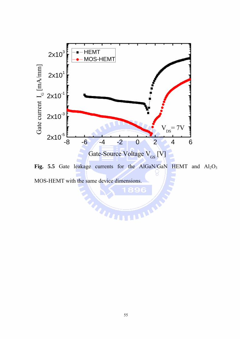

60
-6 -4 -2 0 2 4 60
20
40
60
80
100
120
140GaN 15um MOS-HEMT
Gate-Source Voltage VGS [V]
Tr
ansc
ondu
ctan
ce G
M [m
Sm
m]
4V 5V 6V 7V 8V 9V 10V
Fig 510 Gm versus VGS curve for the Al2O3 MOS-HEMT at the VDS bias is from
4 V to 10V
61
02 03 04 05 06 07 084
8
12
16
20IP3max = 1893 dBm for MOS-HEMT
Third
ord
er in
terc
ept p
oint
IP3
[dB
m]
Idss []
HEMT MOS-HEMT
Fig 511 IP3 versus IDS curve of the the AlGaNGaN HEMT and Al2O3
MOS-HEMT and the test frequency is 2GHz and VDS =7V
62
Table 51 Comparison of the IP3 of Al2O3 MOS-HEMT and HEMT device at
drain bias is 7V
63
Chapter 6
Conclusion
In this dissertation 15-μm-length Al2O3 AlGaNGaN MOS-HEMTs and
HEMTs grown on Silicon substrate were successfully fabricated and the DC and
RF characteristics were evaluated The maximum IDS of 810 mAmm and peak
extrinsic Gm of 747 mSmm were obtained for the GaN HEMT fabricated
However the AlGaNGaN HEMT suffers from high leakage current In order to
solve this problem an insulated Al2O3 gate was applied to the device to suppress
the high gate leakage current The innovative MOS-HEMT technique not only
reduces the leakage current but also successfully improved the linearity
characteristics of the AlGaNGaN HEMTs on Si substrate It is found that
MOS-HEMT effectively reduced the high electric field in the forward bias it
enables the electrons to maintain a stable electron velocity under the gate
domain and further to suppress high gate leakage current The MOS-HEMT
devices demonstrates increased drain current and maintain stable Gm value under
a larger gate bias domain the MOSHEMTs also demonstrated improvement in
the Gm vs VGS curve flatness and thus leads to lower overall IM3 and higher IP3
for even through the regular HEMT exhibits higher peak Gm For the
MOS-HEMT the maximum third order intermodulation point (IP3) of 1893
dBm was achieved in the MOS-HEMT devices The IP3 was higher them the
regular HEMT device
In addition the third order intermodulation points of the MOS-HEMT and
Schottky-gate device under the different gate biases are also compared in this
study By polynomial curve fitting technique It successfully demonstrate that
64
the multi-gate device have the higher IP3 in the larger IDSS region Therefore
it indicated that multi gate technique could effectively improve the linearity
performance
In conclusion the experimental results in this study shows that in the future
the AlGaNGaN HEMTs with Al3O3-insulated gate have great potential to be
used in the RF power amplifier with improved linearity for the modern wireless
communication system
65
References [1] U K Mishra Linkun Shen T E Kazior and Y-F WuldquoGaN-Based RF
Power Devices and Amplifiersrdquo Proceedings of the IEEE vol 96 no 2
pp287-305 Feb 2008
[2] Y Ando Y Okamoto H Miyamoto T Nakayama T Inoue and M
Kuzuhara ldquo10-Wmm AlGaN-GaN HFET with a field modulating platerdquo IEEE
Electron Device Lett vol 24 no 5 pp 289-291 May 2003
[3] Y F Wu M Moore A Saxler T Wisleder and P Parikh ldquo40 Wmm double
field-plated GaN HEMTsrdquo in Proc Dig Device Res Conf pp 151ndash152 Jun
2006
[4] Y FWu A SaxlerMMoore R P Smith S Sheppard PM Chavarkar
TWisleder U KMishra and P Parikh ldquo30-Wmm GaN HEMTs by field plate
optimizationrdquo IEEE Electron Device Lett vol 25 no 3 pp 117-119 Mar
2004
[5] Y Pei et al ldquoRecessed Slant Gate AlGaNGaN High Electron Mobility
Transistors with 209Wmm at 10GHz rdquo Jpn J Appl Phys Vol 46pp
L1087-L10892007
[6] Wu YQ Y Xuan T Shen PD Ye Z Cheng and A Lochtefeld
Enhancement-mode InP n-channel metal-oxide-semiconductor field-effect
transistors with atomic-layer-deposited Al2O3 dielectrics Appl Phys Lett vol
91 no 2 2007
[7] Huang ML YC Chang CH Chang YJ Lee P Chang J Kwo TB
Wu and M Hong Surface passivation of III-V compound semiconductors
using atomic-layer-deposition-grown Al2O3 Appl Phys Lett vol 87 no 25
2005
66
[8] Xuan Y HC Lin PD Ye and GD Wilk Capacitance-voltage studies
on enhancement-mode InGaAs metal-oxide-semiconductor field-effect transistor
using atomic-layer-deposited Al2O3 gate dielectric Appl Phys Lett vol 88
no 26 2006
[9] O Ambachera) J Smart J R Shealy N G Weimann K Chu M
MurphyW J Schaff and L F Eastmanrdquo Two-dimensional electron gases
induced by spontaneous and piezoelectric polarization charges in N- and
Ga-face AlGaNGaN heterostructuresrdquo Journal of Applied Physics vol 85 no
6 15 1999
[10] S Nakamura GaN Growth Using GaN Buffer Layer Jpn J Appl Phys
vol 30 pp L1705-L1707 1991
[11] D Kapolnek et al Structural evolution in epitaxial metalorganic chemical
vapor deposition grown GaN films on sapphire Appl Phys Lett vol 67 pp
1541-1543 1995
[12] L Zhou et al Effect of AlN flux ratio during nucleation layer growth on
the microstructure of GaN films grown by molecular-beam epitaxy Appl Phys
Lett vol 88 p 011916 2006
[13] J C Zhang et al The influence of AlN buffer layer thickness on the
properties of GaN epilayer J Crys Growth vol 268 pp 24-29 2004
[14] D G Zhao et al Surface morphology of AlN buffer layer and its effect
on GaN growth by metalorganic chemical vapor deposition Appl Phys Lett
vol 85 pp 1499-1501 2004
[15] L Meshi et al The reduction of threading dislocations in GaN using a
GaN nanocolumn interlayer Phys Status Solidi (c) vol 5 pp 1645-1647
2008
[16] M J Manfra et al Dislocation and morphology control during
67
molecular-beam epitaxy of AlGaNGaN heterostructures directly on sapphire
substrates Appl Phys Lett vol 81 pp 1456-1458 2002
[17] K Uchida et al Characterization of Double-Buffer Layers and Its
Application for the Metalorganic Vapor Phase Epitaxial Growth of GaN Jpn J
Appl Phys vol 37 pp 3882-3888 1998
[18] L K Li et al High electron mobility AlGaNGaN heterostructures grown
on sapphire substrates by molecular-beam epitaxy Appl Phys Lett vol 76 pp
742-744 2000
[19] Y B Pan et al Reduction of threading edge dislocation density in n-type
GaN by Si delta-doping J Crys Growth vol 286 pp 255-258 2006
[20] A Corrion et al Review of Recent Developments in Growth of
AlGaNGaN High-Electron Mobility Transistors on 4H-SiC by Plasma-Assisted
Molecular Beam Epitaxy IEICE Trans Electron vol E89-C pp 906-912 2006
[21] J P Ibbetson et al Polarization effects surface states and the source of
electrons in AlGaNGaN heterostructure field effect transistors Appl Phys
Lett vol 77 pp 250-252 2000
[22] M Miyoshi et al ldquoMetalorganic Chemical Vapor Deposition and Material
Characterization of Lattice-Matched InAlNGaN Two-Dimensional Electron
Gas Heterostructuresrdquo Appl Phys Express vol 1 p 081102 2008
[23] A Chini et al ldquo21 Amm current density AlGaNGaN HEMTrdquo Electron
Lett vol 39 pp 625-626 2003
[24] S L Rumyantsev N Pala M S Shur ME Levinshtein R GaskaM Asif
Khan and G Simin Generation-Recombination Noise in GaN-based Devices
in GaN-based materials and devices Selected topics in electronics and
systems - v33 eds MSShur and RF Devis World Scientific 2004 ISBN
981-238-844-3
68
[25] EJ Miller XZ Dang HH Wieder PH Asbeck ETYu GJ Sullivan
and JM Redwing ldquoTrap characterization by gate-drain conductance and
capacitance dispersion studies of an AlGaNGaN heterostructure field-effect
transistorrdquo Jpn J Appl vol 87 8070 2000
[26] Shinya MIZUNO Yutaka OHNO Shigeru KISHIMOTO Koichi
MAEZAWA and Takashi MIZUTANI Jpn J Appl Phys vol 41 no 8 pp
5125-5126 Part 1 August 2002
[27]Kim HS I Ok M Zhang F Zhu S Park J Yum H Zhao JC Lee P
Majhi N Goel W Tsai CK Gaspe and MB Santos A study of
metal-oxide-semiconductor capacitors on GaAs In053Ga047As InAs and InSb
substrates using a germanium interfacial passivation layer Appl Phys Lett
93(6)(2008)
[28] Ok I H Kim M Zhang F Zhu S Park J Yum H Zhao D Garcia P
Majhi N Goel W Tsai CK Gaspe MB Santos and JC Lee Self-aligned
n-channel metal-oxide-semiconductor field effect transistor on
high-indium-content In053Ga047As and InP using physical vapor deposition
HfO2 and silicon interface passivation layer Appl Phys Lett 92(20)(2008)
[29] Zhao H HS Kim F Zhu M Zhang I Ok SI Park JH Yum and JC
Lee Metal-oxide-semiconductor capacitors on GaAs with germanium nitride
passivation layer Appl Phys Lett 91(17) (2007)
[30] Oktyabrsky S V Tokranov M Yakimov R Moore S Koveshnikov W
Tsai F Zhu and JC Lee High-k gate stack on GaAs and InGaAs using in situ
passivation with amorphous silicon Mater Sci Eng B-Solid State Mater Adv
Technol 135(3) P272-276 (2006)
[31] Zhao H JH Yum YT Chen and JC Lee In053Ga047As
n-metal-oxide-semiconductor field effect transistors with atomic layer deposited
69
Al2O3 HfO2 and LaAlO3 gate dielectrics J Vac Sci Technol B 27(4)
P2024-2027 (2009)
[32] Xuan Y YQ Wu T Shen T Yang and PD Ye High performance
submicron inversion-type enhancement-mode InGaAs MOSFETs with ALD
Al2O3 HfO2 and HfAlO as gate dielectrics IEEE New York Vols 1 and 2
p637-640 (2007)
[33] OConnor E RD Long K Cherkaoui KK Thomas F Chalvet IM
Povey ME Pemble PK Hurley B Brennan G Hughes and SB Newcomb
In situ H2S passivation of In053Ga047AsInP metal-oxide-semiconductor
capacitors with atomic-layer deposited HfO2 gate dielectric Appl Phys Lett
92(2)(2008)
[34] S M SZE Semiconductor devices physics and technology 2nd edition
Wiley (2002)
[35] T Ytterdal Y Cheng and T A Fjeldly Devices Modeling for analog and
RF CMOS Circuit Design John Wiley and Sons(2003)
Devices 55(2) P547-556 (2008)
Wiley(2007)