Embed Size (px)
Citation preview
24
CHAPTER -1
INTRODUCTION
1.1 Organic molecular semiconductors
1.2 Phthalocyanines
1.2.1 Mononuclear phthalocyanine
1.2.2 Binuclear phthalocyanine
1.3 Growth modes of molecular semiconductor thin films
1.4 Thin film deposition methods
1.4.1 Molecular beam epitaxy
1.4.2 Solution method
1.5 Outline of thesis
Chapter-1: Introduction
25
1.1 Organic molecular semiconductors
Organic semiconductors are organic materials that exhibit semiconductor properties.
Generally almost all organic solids are insulators. However, when their constituent molecules
have π-conjugate systems and they are appropriately doped, charge carriers (electrons or
holes) can move via π-electron cloud overlaps, especially by hopping, tunnelling and related
mechanisms. Organic semiconductors can be classified into two major classes: (i) molecular
semiconductors e.g. single molecules (polycyclic aromatic compounds, such as, pentacene,
rubrene, anthracene, porphyrine, phthalocyanines etc) and oligomers (short chain i.e. having
few monomers) and (ii) conjugated polymers: which consist of many monomers bonded
together in a long chain e.g. poly(3-alkylthiophene), poly(p-phenylene vinylene),
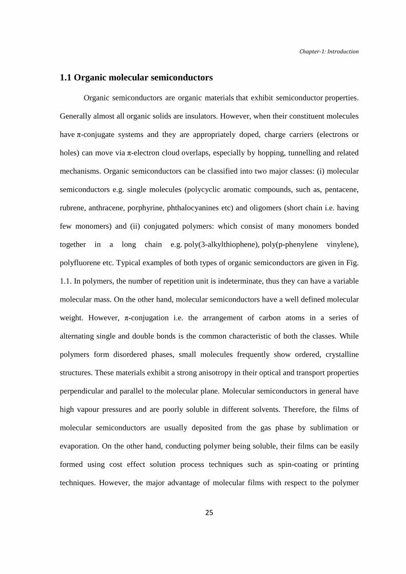
polyfluorene etc. Typical examples of both types of organic semiconductors are given in Fig.
1.1. In polymers, the number of repetition unit is indeterminate, thus they can have a variable
molecular mass. On the other hand, molecular semiconductors have a well defined molecular
weight. However, π-conjugation i.e. the arrangement of carbon atoms in a series of
alternating single and double bonds is the common characteristic of both the classes. While
polymers form disordered phases, small molecules frequently show ordered, crystalline
structures. These materials exhibit a strong anisotropy in their optical and transport properties
perpendicular and parallel to the molecular plane. Molecular semiconductors in general have
high vapour pressures and are poorly soluble in different solvents. Therefore, the films of
molecular semiconductors are usually deposited from the gas phase by sublimation or
evaporation. On the other hand, conducting polymer being soluble, their films can be easily
formed using cost effect solution process techniques such as spin-coating or printing
techniques. However, the major advantage of molecular films with respect to the polymer
Chapter-1: Introduction
26
films is that they can be grown with very high purity and crystalline order, which are the two
major requirements for obtaining high charge carrier mobility.
N
O N
O
N
O
Al
nR R
nS
S
R
R
n
N
N N
N
F
F
FF
F
F
F
F
F
F
FF
F
F
FF
N
N
N
N Cu
N
N
N
N
Co
PPV PFO P3AT
CoPcAlq3
Pentacene
N
N
N
N
N
N
N
N
SO
ONaO
S O
O ONa
SO
OONa
SO
ONaO
Cu
CuPcTs F16CuPc
Figure 1.1 Molecular structures of conducting polymers: PPV: poly(p-phenylenevinylene), PFO:
polyfluorene, P3AT: poly(3-alkylthiophene), Alq3: tris(8-hydroxyquinoline)aluminium, CoPc: Co-
phthalocyanine, pentacene, CuPcTs: copper phthalocyanine tetrasulfonate and F16CuPc: Copper
hexadecafluorophthalocyanine.
Chapter-1: Introduction
27
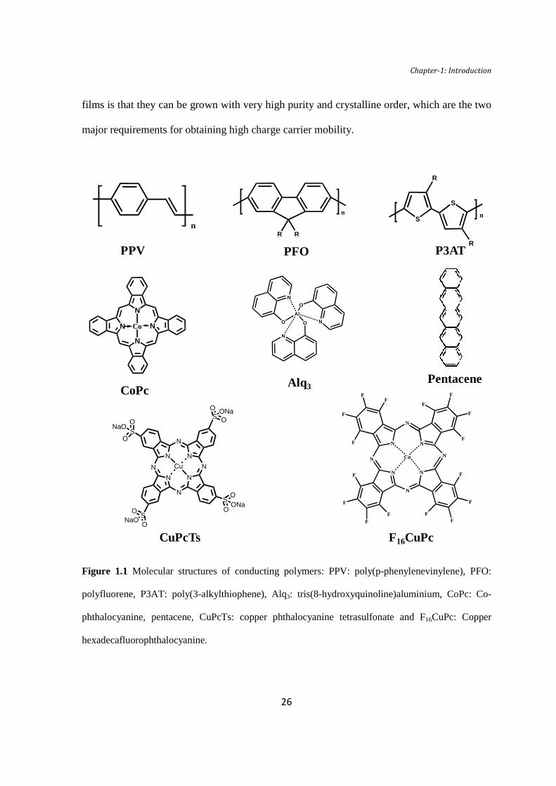
Characteristics of molecular semiconductors are the intramolecular bonds. The
alternation of single (σ) and double (π) bonds, referred to as conjugation, is responsible for
semiconductor nature of organic molecular. In a conjugated system, the carbon atoms
involved in the conjugation are sp2 hybridized (the 2s orbital is mixed with only two of the
three available 2p orbitals) which means the three hybrid sp2 orbitals form the σ bonds, with
the σ-electrons being highly localized, leaving the pz orbital unaltered. The mutual overlap
between remaining non hybridized pz orbitals of adjacent carbons leads to the formation of π
bonds. The electrons of overlapping pz orbitals form a delocalized electronic orbital over the
whole conjugation length. These π electrons are delocalized over the whole molecule and are
more loosely bound compared to the σ electrons These delocalized electrons responsible for
semiconducting properties of this class of materials. As an example this is illustrated in Fig.
1.2 for benzene molecule.
Figure 1.2 Schematics representation of π-orbitals in benzene (C6H6) molecule, responsible of its
semiconducting nature. In the solid the overlap between π -orbitals of adjacent molecule will allow
the charge transport through the solid.
Chapter-1: Introduction
28
π*
π
HOMO
LUMO
Eg
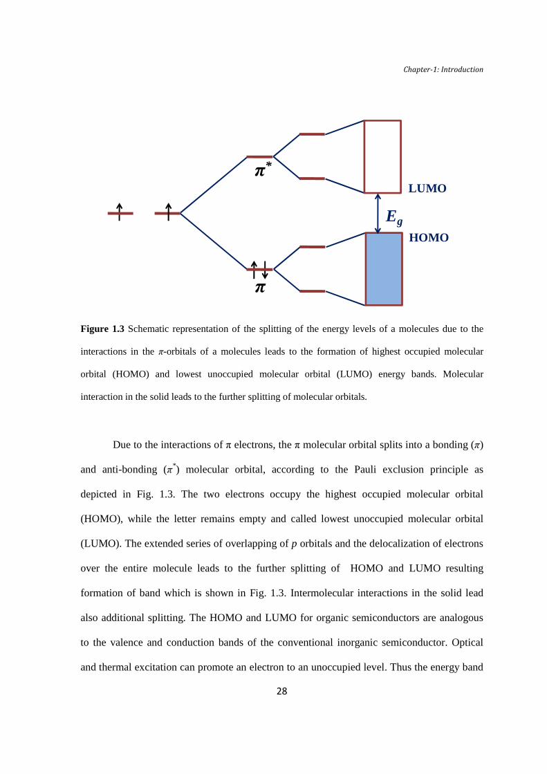
Figure 1.3 Schematic representation of the splitting of the energy levels of a molecules due to the
interactions in the π-orbitals of a molecules leads to the formation of highest occupied molecular
orbital (HOMO) and lowest unoccupied molecular orbital (LUMO) energy bands. Molecular
interaction in the solid leads to the further splitting of molecular orbitals.
Due to the interactions of π electrons, the π molecular orbital splits into a bonding (π)
and anti-bonding (π*) molecular orbital, according to the Pauli exclusion principle as
depicted in Fig. 1.3. The two electrons occupy the highest occupied molecular orbital
(HOMO), while the letter remains empty and called lowest unoccupied molecular orbital
(LUMO). The extended series of overlapping of p orbitals and the delocalization of electrons
over the entire molecule leads to the further splitting of HOMO and LUMO resulting
formation of band which is shown in Fig. 1.3. Intermolecular interactions in the solid lead
also additional splitting. The HOMO and LUMO for organic semiconductors are analogous
to the valence and conduction bands of the conventional inorganic semiconductor. Optical
and thermal excitation can promote an electron to an unoccupied level. Thus the energy band
Chapter-1: Introduction
29
gap for organic semiconductor corresponds to the gap between HOMO and LUMO of the
molecule. The HOMO-LUMO separation in these conjugated molecules depends strongly on
the overlapping of neighbouring p orbitals, which is in turn related to the planarity of the
molecule and to side groups. In many cases, the HOMO-LUMO energy gap is relatively
small (~ 1 to 3 eV) and the molecules can be doped to assume n- or p-type character. Thus,
the π-conjugated molecules can act as semiconducting channels in organic molecular devices.
However the band formation is not sufficient for organic molecular material to behave as
semiconductor, there must be a mechanism of charge carrier transport between molecules.
This is achieved due to the overlap of the π-orbitals from one molecule to those of its
neighbouring molecule. Therefore a close packing of molecule and a crystalline structure of
free of defects is essential to maximize the π-orbital overlap and thus improve the conduction
properties of the material. The low molecular symmetry leads to highly anisotropic
conduction parameters since the effective path for charge carrier transport is perpendicular to
molecular plane, direction of maximum π-overlap [1]. Thus, parameters like the charge
carrier mobility must be described by a mobility tensor µij [2, 3]. In general, all physical
properties of these materials may present anisotropic behaviour due to low symmetry of
molecular constituents and the low-symmetry crystalline structure they form.
During past few decades, organic semiconductors have attracted significant and
increasing interest due to their interesting electrical and optical properties. Their applications
in flexible and low cost, and tuning possibilities in the manufacturing electronic devices
make them suitable candidates for future electronic devices [4-7]. Moreover, organic
molecules are potential candidate for pushing the existing scaling limits of the existing
silicon based microelectronics to nanoscale [8-10]. The advantages offered by the organic
Chapter-1: Introduction
30
molecules to be used in the nanoscale devices are: (i) small size (typically 0.5 to 2.5 nm), (ii)
easy tuning of electronic properties by changing chemical structure of the molecule, and (iii)
possibility of forming self–assembled monolayer on various substrates (e. g. thiols on Au,
silanes on Si) . In recent years, various nanoelectronics molecular devices, such as, rectifiers,
memory, resonant tunnel diodes and transistors have been demonstrated using two-
dimensional ordered molecular monolayers and multilayers [11-13]. The interest in electrical
properties of organic monolayers has developed enormous academic interest in this field [14-
18]. Similarly, thin and thick films of various organic semiconductors are actively being
investigated from the view point of understanding the physics underlying the charge transport
as well as their applicability in new electronic applications e.g. flexible and low cost large
area electronics, which is difficult to achieve using inorganic semiconductors. This research
field is growing very fast. At present researchers are able to manage the material properties at
the molecular level [19]. Moreover, many efforts are being made in the industrial
development of the organic electronic devices. Many applications of organic semiconductors
have been already demonstrated and some of them are commercially available in market.
These include: mobile phones display based on organic field effect transistor (OFET) by
Philips and Polymer Vision, automobile stereo display from Pioneer, organic light emitting
devices (OLEDs) from Philips and full color displays Kodak digital cameras. On the
development of organic electronics, Forest has commented: “If the field continues to
progress at its current, rapid pace, electronics based on organic thin-films materials will
soon become a mainstay of our technological existence” [20]. However, despite of these
developments, organic devices have limitation in terms of their low charge carrier mobility
(0.001-10 cm2 /Vs) [16, 21, 22], which is several orders of magnitude lower than traditional
Chapter-1: Introduction
31
inorganic semiconductor (e.g. Silicon 1400 cm2 /Vs). In order to improve the performance of
organics devices, it is necessary that their mobility need to be increased.
1.2 Phthalocyanines
The word Phthalocyanine is derived from the Greek term 'naphtha' (rock oil) and
'cyanine' (dark blue). The first phthalocyanine was produced accidentally in 1907 by Braun
and Tcherniac as a minor product in the synthesis of o-cyanobenzamide from phthalamide
and acetic anhydride [23]. C. E. Dent et al. reported the structure of the planar
phthalocyanine molecule for the first time [24]. Phthalocyanines are an intensely blue-green
coloured macrocyclic compound and traditionally have been used as dyes or
pigments. Phthalocyanines form coordination complexes with most elements of the periodic
table and exhibit semiconducting properties. Therefore they are currently being explored for
their possible applications in the organic electronics. Majority of the research has been
carried out on the mononuclear phthalocyanines i.e. molecule containing only one metal
atom. However, phthalocyanines can form dimmers, in which two mononuclear
phtahlocyanine (with similar or different metal atoms) units are covalently linked. Here we
briefly overview the structural properties of mononuclear as well as binuclear
phthalocyanines.
1.2.1 Mononuclear phthalocyanine
The metal-free phthalocyanine (H2Pc) has the general formula C32H18N8. It is
chemically designated as 5, 10, 15, 20 tetraazatetrabenzporphyrin or tetrabenzporphyrazin
Chapter-1: Introduction
32
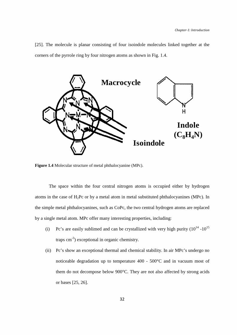
[25]. The molecule is planar consisting of four isoindole molecules linked together at the
corners of the pyrrole ring by four nitrogen atoms as shown in Fig. 1.4.
Macrocycle
Isoindole
Indole(C8H4N)
Figure 1.4 Molecular structure of metal phthalocyanine (MPc).
The space within the four central nitrogen atoms is occupied either by hydrogen
atoms in the case of H2Pc or by a metal atom in metal substituted phthalocyanines (MPc). In
the simple metal phthalocyanines, such as CoPc, the two central hydrogen atoms are replaced
by a single metal atom. MPc offer many interesting properties, including:
(i) Pc’s are easily sublimed and can be crystallized with very high purity (1014 -1015
traps cm-3) exceptional in organic chemistry.
(ii) Pc’s show an exceptional thermal and chemical stability. In air MPc’s undergo no
noticeable degradation up to temperature 400 - 500°C and in vacuum most of
them do not decompose below 900°C. They are not also affected by strong acids
or bases [25, 26].
Chapter-1: Introduction
33
(iii) Pc’s is highly conjugated molecule and contains 18 π electrons in the
macrocyclic ring which leads to very intense absorption bands at around 400 nm
and 700 nm.
(iv) Pc’s are a very versatile system as there are possibilities of tuning its electronic
properties by playing with different side group and central metal atoms. There are
more than thousand different Pc’s have been synthesized by changing either
central metal atom or side groups. The replacement of central metal atom and side
group modifies its electronic properties, while its molecular structure, in most of
the cases, remains unchanged [25, 26]. For example CuPc is a p-type molecular
semiconductor but the replacement of 16 hydrogen by fluorine makes the
molecule (F16CuPc) n-type. In fact, F16CuPc is one of the most stable n-type
organic semiconductor known at present, and it has been used to fabricate the first
n-channel organic transistor [27], and in complementary logic circuits [28, 29].
Due to the above properties, metal phthalocyanines have been intensely investigated
for various organic devices, such as solar cells, OLEDs, OFETs and gas sensors [30-35].
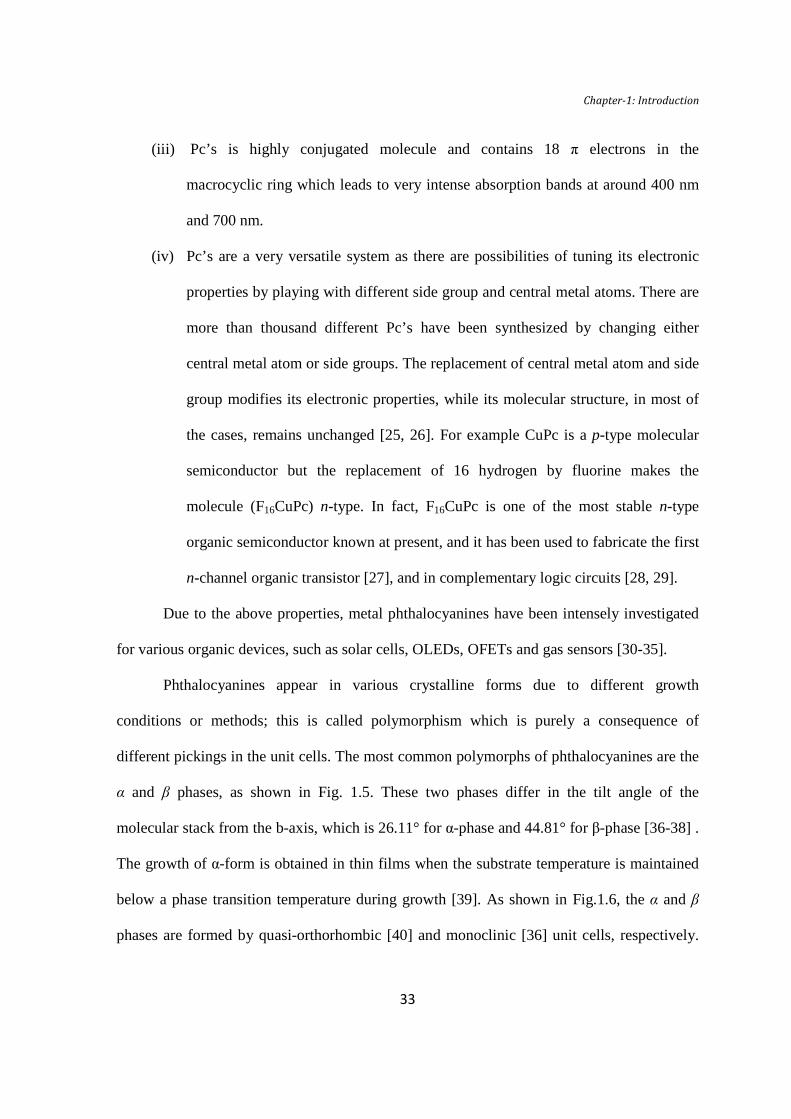
Phthalocyanines appear in various crystalline forms due to different growth
conditions or methods; this is called polymorphism which is purely a consequence of
different pickings in the unit cells. The most common polymorphs of phthalocyanines are the
α and β phases, as shown in Fig. 1.5. These two phases differ in the tilt angle of the
molecular stack from the b-axis, which is 26.11° for α-phase and 44.81° for β-phase [36-38] .
The growth of α-form is obtained in thin films when the substrate temperature is maintained
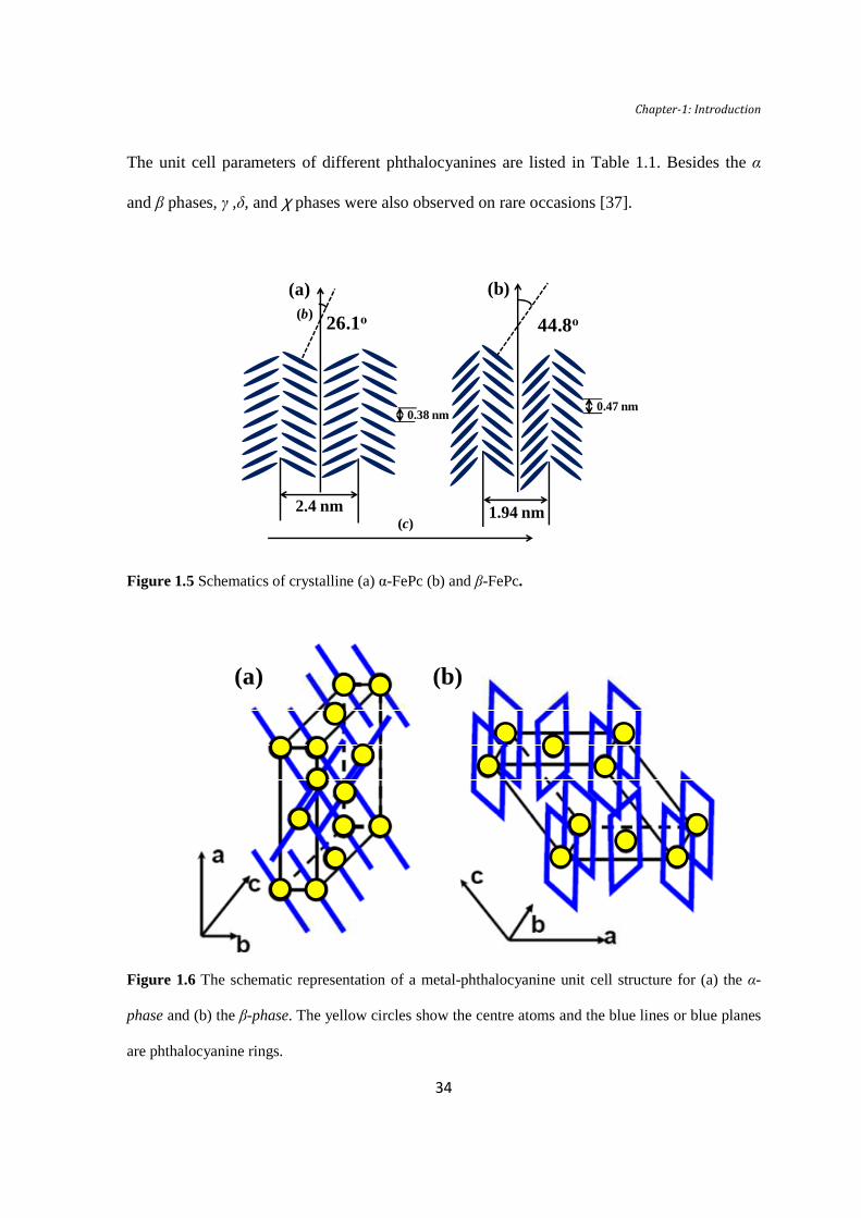
below a phase transition temperature during growth [39]. As shown in Fig.1.6, the α and β
phases are formed by quasi-orthorhombic [40] and monoclinic [36] unit cells, respectively.
Chapter-1: Introduction
34
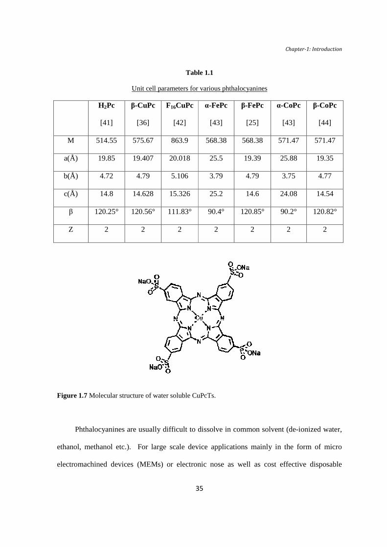
The unit cell parameters of different phthalocyanines are listed in Table 1.1. Besides the α
and β phases, γ ,δ, and χ phases were also observed on rare occasions [37].
26.1ο 44.8ο
(a) (b)
2.4 nm 1.94 nm(c)
(b)
0.38 nm0.47 nm
Figure 1.5 Schematics of crystalline (a) α-FePc (b) and β-FePc.
(a) (b)
Figure 1.6 The schematic representation of a metal-phthalocyanine unit cell structure for (a) the α-
phase and (b) the β-phase. The yellow circles show the centre atoms and the blue lines or blue planes
are phthalocyanine rings.
Chapter-1: Introduction
35
Table 1.1
Unit cell parameters for various phthalocyanines
H2Pc
[41]
β-CuPc
[36]
F16CuPc
[42]
α-FePc
[43]
β-FePc
[25]
α-CoPc
[43]
β-CoPc
[44]
M 514.55 575.67 863.9 568.38 568.38 571.47 571.47
a(Å) 19.85 19.407 20.018 25.5 19.39 25.88 19.35
b(Å) 4.72 4.79 5.106 3.79 4.79 3.75 4.77
c(Å) 14.8 14.628 15.326 25.2 14.6 24.08 14.54
β 120.25° 120.56° 111.83° 90.4° 120.85° 90.2° 120.82°
Z 2 2 2 2 2 2 2
Figure 1.7 Molecular structure of water soluble CuPcTs.
Phthalocyanines are usually difficult to dissolve in common solvent (de-ionized water,
ethanol, methanol etc.). For large scale device applications mainly in the form of micro
electromachined devices (MEMs) or electronic nose as well as cost effective disposable
Chapter-1: Introduction
36
sensors, it is necessary to manufacture the sensors by simpler technique such as solution
spinning, printing, micro-drop coating, etc. Water soluble phthalocyanine can also be
synthesized from non-substituted phthalocyanines by attaching sulfonate groups [45]. A
typical example of water-soluble phthalocyanines is copper (II) phthalocyanine tetrasulfonic
acid, tetrasodium salt (CuPcTs), and its structure is shown in Fig. 1.7. The structure of
CuPcTs is very similar to CuPc except that polar SO3Na attached to the corners of benzene
rings and makes this compound water soluble [45]. These water soluble phthalocyanines
have been used as FET and gas sensors [46, 47].
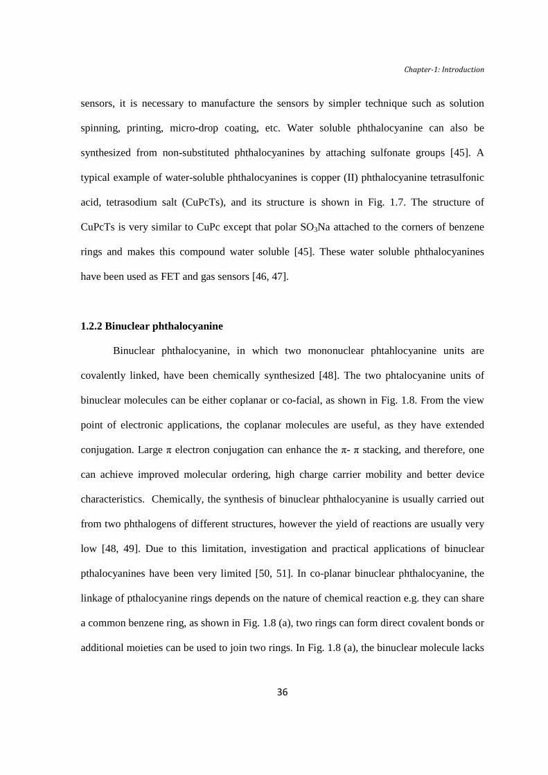
1.2.2 Binuclear phthalocyanine
Binuclear phthalocyanine, in which two mononuclear phtahlocyanine units are
covalently linked, have been chemically synthesized [48]. The two phtalocyanine units of
binuclear molecules can be either coplanar or co-facial, as shown in Fig. 1.8. From the view
point of electronic applications, the coplanar molecules are useful, as they have extended
conjugation. Large π electron conjugation can enhance the π- π stacking, and therefore, one
can achieve improved molecular ordering, high charge carrier mobility and better device
characteristics. Chemically, the synthesis of binuclear phthalocyanine is usually carried out
from two phthalogens of different structures, however the yield of reactions are usually very
low [48, 49]. Due to this limitation, investigation and practical applications of binuclear
pthalocyanines have been very limited [50, 51]. In co-planar binuclear phthalocyanine, the
linkage of pthalocyanine rings depends on the nature of chemical reaction e.g. they can share
a common benzene ring, as shown in Fig. 1.8 (a), two rings can form direct covalent bonds or
additional moieties can be used to join two rings. In Fig. 1.8 (a), the binuclear molecule lacks
Chapter-1: Introduction
37
a benzene ring this is referred to as the (-1) linked binuclear phthalocyanine [52]. This type
of binuclear phthalocyanine has been used for electrochemical sensors [53]. There are some
reports where the monolayer/multilayers of binuclear phthalocyanine have been prepared
using Langmuir-Blodgett (LB) technique or by drop casting method [50, 51]. In these
studies, first the synthesis of precursor binuclear phthalocyanine was carried out and then
films were prepared by LB technique. However there are no reports on the growth of
binuclear phthalocyanine films using physical vapor deposition.
N
NN
N
N
NN N N
N
N
NN
N
N
N
Co Co
HO3S
HO3S
SO3H SO3H
SO3H
SO3H(a) (b)
Figure 1.8 Chemical structure of (a) coplanar and (b) co-facial binuclear phthalocyanine molecules.
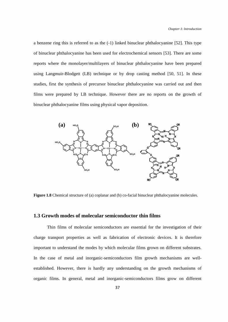
1.3 Growth modes of molecular semiconductor thin films
Thin films of molecular semiconductors are essential for the investigation of their
charge transport properties as well as fabrication of electronic devices. It is therefore
important to understand the modes by which molecular films grown on different substrates.
In the case of metal and inorganic-semiconductors film growth mechanisms are well-
established. However, there is hardly any understanding on the growth mechanisms of
organic films. In general, metal and inorganic-semiconductors films grow on different
Chapter-1: Introduction
38
substrates by three different modes, which depends on the relative surface energy between
substrate and films as well as on the lattice mismatch [i.e. (as - af)/af, where as and af are,
respectively, lattice parameter of the substrate and the film]:
Layer by layer growth
Layer plus island growth
Island growth
(a) (b) (c)
Figure 1.9 Schematic representations of three different growth modes of thin films (a) Frank-van der
Merwe mode, (b) Volmer–Weber mode (c) Stranski– Krastanov mode.
(i) Frank-van der Merwe mode: In this mode layer-by-layer growth occurs if the
interaction between the substrate and film atoms is stronger than that between
neighboring films atoms the lattice mismatch is zero, as shown in Fig. 1.9 (a).
Each new layer starts to grow only when the last one has been completed.
(ii) Volmer–Weber mode: In this mode the film grows in the form of separate 3D
islands to minimize the overall surface energy, if the interaction between the
Chapter-1: Introduction
39
neighboring films atoms stronger than the over layer substrate interaction, as
shown in Fig. 1.9 (b).
(iii) Stranski– Krastanov mode: This layer-plus-island growth mode is an interesting
intermediate case. In this mode one or sometimes several complete monolayers
form first, followed by individual. This mixed growth mode occurs due to large
lattice mismatch although interaction between the substrate and film atoms is
stronger than that between neighboring films atoms, as shown in Fig. 1.9 (c).
Figure 1.10 A simplified picture of an island formation: γS is the surface free energy of substrate, γF
is the free energy of the film material and γI is the interface energy of the film-substrate
The above mentioned growth modes can be described using Young’s equation that
takes surface energies and interface energy into account, as schematically shown in Fig. 1.10.
According to Young’s equation, wetting angle of a liquid nucleus on substrate can be
expressed as:
γS = γI + γF cos φ
Chapter-1: Introduction
40
where γS is the surface free energy of substrate, γF is the free energy of the film material and
γI is the interface energy of the film-substrate. Using the Young’s equation the two limiting
growth modes, layer by layer and island can be distinguished by the angle φ,
(i) layer growth : φ = 0, γS > γI + γF
(ii) island growth: φ > 0, γS < γI + γF
The layer-plus-island growth can easily be explained by assuming a lattice mismatch
between deposited film and substrate. The lattice of the films tries to adjust to substrate
lattice, but at the expense of elastic deformation energy. The transition from layer to island
growth occurs when the spatial extent of the elastic strain field exceeds the range of adhesion
forces within the deposited material.
Surface diffusion
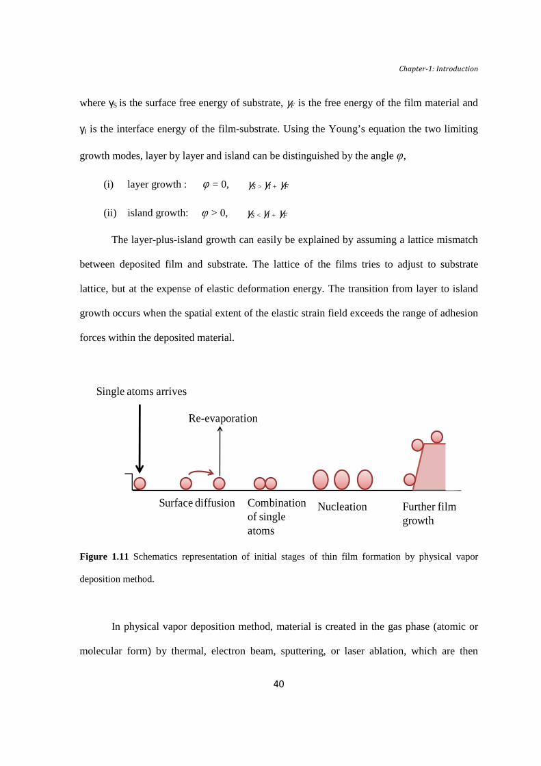
Single atoms arrives
Re-evaporation
Combination of single atoms
Nucleation Further film growth
Figure 1.11 Schematics representation of initial stages of thin film formation by physical vapor
deposition method.
In physical vapor deposition method, material is created in the gas phase (atomic or
molecular form) by thermal, electron beam, sputtering, or laser ablation, which are then
Chapter-1: Introduction
41
allowed to deposit on the surface of the substrate. The individual atomic processes occurring
during the formation of a film on the surface of substrate that determine growth mode are
illustrated in Fig. 1.11. The surface of the substrate is covered with large number of
absorption sites and a molecule becomes bound to one of these with characteristics energy.
The absorbed atoms do not remain stationary but may re-evaporate; requiring energy equal to
adsorption energy, or it may diffuse or hop to adjacent sites. In all these process,
characteristics activation energies have to be overcome. Other processes are collision and
recombination. Each group of atoms eventually reaches a size that is more likely to grow
than decay. The formation of such island of material is known as nucleation. The next stage
of thin film formation is coalescence, in which individual island continue to grow by addition
of more atoms, until they touch one another to form continuous network.
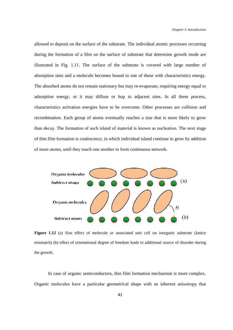
Figure 1.12 (a) Size effect of molecule or associated unit cell on inorganic substrate (lattice
mismatch) (b) effect of orientational degree of freedom leads to additional source of disorder during
the growth.
In case of organic semiconductors, thin film formation mechanism is more complex.
Organic molecules have a particular geometrical shape with an inherent anisotropy that
Chapter-1: Introduction
42
differs from the intrinsic isotropy of inorganic atoms. Molecules are composed of covalent
bonds between neighboring atoms and molecule-molecule interactions are usually weak van
der Waals forces [54]. In addition, the chemical interaction between molecule and substrate
can strongly influence the growth mode. Therefore, growth modes of molecular films are
quite complicated. Typical relationship between organic molecules and inorganic substrates
are shown in Fig. 1.12, and some key issues that can lead to uniquely different growth modes
in comparison to inorganic counterparts are as follows.
(i) Organic molecules are ‘extended objects’ and thus have internal degrees of
freedom. This is probably the most fundamental difference between growth of
atomic and growth of organic molecular systems. The orientational degrees of
freedom which are not included in conventional growth models can give rise to
qualitatively new phenomena, such as the change of the molecular orientation
during film growth, as shown in Fig. 1.12 (b). Also, even without considering a
transition during the growth, the distinction of ‘lying-down’ and ‘standing-up’
films is important and obviously only possible for molecular systems. The
vibrational degrees of freedom can have an impact on the interaction with the
surface as well as the thermalization upon adsorption and the diffusion behavior
[55].
(ii) In contrast to the inorganic semiconductor where each ad-molecule is a single
atoms with spherical symmetry, for organic molecule like phthalocyanine each
ad-molecule involve more than 50 covalently bounded atoms, forming a unit with
low symmetry. The size of molecule and associated unit cell are in nanometer
Chapter-1: Introduction
43
scale, and thus, deposition on inorganic substrate presents lattice mismatches of
one order of magnitude, as shown in Fig. 2.12 (a) [56].
(iii) The interactions between molecules as well as between molecules and substrate
are often dominated by weak van der Waals forces. It is important to emphasize
that when integrated over all atoms within a molecule, the weak interaction
energies add up and lead to substantial molecular binding energies in the eV
range. Nevertheless the weaker interactions per atom lead to ‘softer’ materials
and, for example, strain can be accommodated more easily. Due to the weaker
interactions the thermal expansion coefficients (typically in the 10-4 K-1 range) are
large when compared to inorganic materials, which possibly leads to higher
thermally induced strain at film–substrate interfaces.
(iv) Since we are concerned with closed-shell molecules and van der Waals type
crystals, there are no dangling bonds at the organic surface, and thus the surface
energies are usually weaker than for inorganic substrates.
Generally, most of the above points directly or indirectly impact the interactions and
thus also the barriers experienced during diffusion. Thus, not only the static structure, but
also the growth dynamics exhibit differences compared to inorganic systems.
1.4 Thin film deposition methods
In principle, all the techniques used for making inorganic thin films (e.g. thermal,
electron beam, sputtering, molecular beam epitaxy, laser ablation, solution methods etc) can
be used for the deposition of the molecular semiconductor thin films. However, depending
Chapter-1: Introduction
44
upon the solubility of the molecular semiconductors, organic films are deposited by
following two major techniques:
(i) Physical vapor deposition
(ii) Solution processing
In the physical vapor deposition, the molecular semiconductor is vaporized or
sublimated and, molecules get deposited onto a substrate to form a film. For solution
deposition, the molecular semiconductor is completely dissolved in an organic solvent. The
solution is then coated onto the substrate by either drop-casting, spin-coating, dip-coating, or
printing. Vapor deposition normally yields more uniform films that can be controlled using
various growth parameters, such as, deposition rate, substrate temperature etc. and therefore,
is commonly used for fabricating organic electronic devices. It has also the advantages of
providing a clean environment during film deposition. One of the most used methods is
organic molecular beam epitaxy (OMBE), which imitates the molecular beam epitaxy (MBE)
of inorganic thin films. OMBE provides a fine control over the deposition rate e.g. a rate of 1
monolayer/min can be easily be achieved by controlling the effusion cell temperature.
Solution processing, on the other hand, is a relatively fast and low-priced method of
fabricating thin molecular films. However, in this method film uniformity, control of
crystallinity etc. are usually difficult to control. In the following we present an overview the
literature on the organic film deposition by OMBE and solution process methods.
1.4.1 Molecular beam epitaxy
In 1989 Hera et al. reported first study on the growth of organic molecule CuPc on
cleaved face of MoS2 using MBE [57]. MBE provides the path for best possible control of
Chapter-1: Introduction
45
growth conditions in clean environmental [56] and this has triggered growth of several
organic films using MBE [56, 58-61]. Despite of several studies, the growth behavior of
organic films deposited using MBE is not fully understood. As discussed earlier, the unit cell
of molecular semiconductors are much larger than those of inorganic substrates. Thus the
lattice matching condition does not occur, which makes the epitaxial growth of molecular
semiconductors very difficult. Recently, van der Waals epitaxy (vdE) term has been coined
to refer an epitaxial growth of molecular film on weakly interacting substrate [58]. A
mismatch between the substrate and film lattices results in “strained van der Waals epitaxy”,
although for highly strained growth, epitaxial structures tend to relax at a critical thickness,
thus generating defects [56]. Following van der Walls epitaxy a number of studies have been
reported on MBE growth of organic molecular thin films. The most extensive studies of
epitaxial growth of organic molecular films have been concentrated on phthalocyanines films
on ionic substrate such as alkali halide substrate, metals and on passivated substrate of
Si(111) and GaAs(111) [56, 58, 59]. Recently a new method called weak epitaxy growth
(WEG) has been developed for the deposition of high-quality organic semiconductor thin
films. “Weak” means to decrease the interaction between the molecules and the substrate by
way of introducing a buffer layer [62, 63] . Using WEG method layer-by-layer growth of n-
type F16CuPc on the monolayer p-sexiphenyl (p-6P) on SiO2 substrate with roughness less
than 1 nm has been reported [63]. Highly orientated crystalline films of p-type
phthalocyanine were also fabricated by WEG method [64, 65].
Recently Soumen has investigated in detail the growth of phthalocyanine films using
OMBE on different substrates. He has demonstrated that (i) due to high vapor pressures of
pthalocyanines, the growth temperatures are < 200˚C, which are much lower than used in
Chapter-1: Introduction
46
inorganic films deposition, (ii) The molecule-substrate interaction plays a dominant role in
the growth mode of growth of phthalocyanine films e.g. if the molecule-substrate interaction
is strong e.g. in case of (0001) sapphire then the molecule stack in face-on configuration,
whereas for weakly interacting substrates e.g. glass or quartz, the molecules stack in the
edge-on configuration. (iii) The controlled defects e.g. twin boundaries in (100) LaAlO3
substrates or grain boundary of a bicrystal (100) substrate act as a template for the growth of
highly ordered phthalocyanine films [3, 66, 67].
1.4.2 Solution method
If the molecules are thermal unstable and has a finite solubility in certain solvents
then solution process is useful technique for deposition of the molecular films. In this
method, molecules are dissolved in an appropriate solvents and the solution is coated on
substrates using different methods, such as, spin coating, drop casting, doctor balding or ink-
jet printing. In spin coating techniques, a drop of solution is applied to the substrate which is
placed on a rotating substrate with high speed around 2000 rpm. The solution spreads on the
substrates and dries rapidly as it rotates leaving a solid film. In doctor balding technique, a
solution containing the soluble molecule is spread with uniform thickness by means of
“doctor blade”. Although by solution process techniques it is expected to produce a films in
which individual molecule are relatively disordered, but this is not always true. There are
many reports on organized layer of organic molecule deposited by solution process [7, 68].
Furthermore by spin coating high-quality continuous films of uniform thickness of same
crystalline order similar to that of Langmuir-Blodgett (LB) films of analogous compounds
can be produced. The requirement is that the materials are significantly soluble in volatile
Chapter-1: Introduction
47
solvents without the necessity for surface activity. The main advantages of solution process
techniques are easy and low cost, and large area deposition can be easily made.
1.5 Outline of thesis
This thesis is focused on the deposition of phthalocyanine films using both molecular
beam epitaxy as well as solution process techniques and to investigate their charge transport
properties as a function of applied electric field and temperature. The main objectives are:
(i) Growth of mononuclear phthalocyanine p-type FePc, CoPc and n-type F16CuPc
films using MBE.
(ii) Growth of binuclear (Co-Fe)Pc films by MBE using CoPc and FePc as the source
materials.
(iii) Deposition of mononuclear phthalocyanine CuPcTs films by solution process.
(iv) Investigation of the charge transport in mononuclear p-type CoPc, FePc, binuclear
(Co-Fe)Pc, and n-type F16CuPc films as a function of bias and temperature.
(v) Growth and characterization of p-type/n-type bilayer heterostructure by MBE and
their charge transport studies.
(vi) Studies on the gas sensing characteristics of various pthalocyanine films.
The thesis comprising of various experimental technique used during the thesis work,
and various results obtained on the studies mentioned above is organized as follows.
In Chapter 2 the various experimental techniques are discussed. The details of MBE
system used for the deposition of phthalocyanine films and heterostructures are described. A
brief description of the characterization techniques, such as Scanning electron microscopy
(SEM), Atomic force microscopy (AFM), X-ray photoelectron spectroscopy (XPS), Fourier
Chapter-1: Introduction
48
transform infrared (FTIR) spectroscopy, UV-Visible spectroscopy, Kelvin probe microscopy
are presented. The set up used for the measurements of charge transport and gas sensing
characteristics are presented.
In Chapter 3, details of the growth of mononuclear CoPc, FePc and binuclear (Co-
Fe)Pc films by MBE are presented. Charge conduction in FePc films under high electrical
field are presented. A bias dependent transition from ohmic to space-charge limited
conduction to space charge limited conduction with field enhanced mobility is observed. At
temperatures <100 K, by analyzing the low bias (< 100 V) data, which is governed by
Schottky – barrier limited conduction. However at higher bias multistep tunnelling was
observed in the FePc films.A novel feature i.e. temperature dependent metal to insulator like
transition, has been observed in ultrathin CoPc films deposited on (001) SrTiO3 substrates.
In-plane compressive strains induced by structural phase transition of SrTiO3 substrate
reduce the intermolecular distance, and as a result, metallic behavior is observed. Binuclear
(Co-Fe)Pc films were found to grown only on sapphire substrates at 200°C if deposited using
the CoPc/FePc mixture in 1:1 (w/w) ratio. Formation of binuclear was confirmed by Multi
Assisted Laser Desorption and Ionization (MALDI) mass spectroscopy. The binuclear (Co-
Fe)Pc films exhibited charge carrier mobility of ~110 cm2/Vs, which is around two order of
magnitude higher than CoPc and FePc films.
In Chapter 4, the deposition and characterization of p-type CoPc/ n-type F16CuPc
heterojunction are presented. The results on the charge transport Kelvin Probe studies on
these heterostructures are presented.
In Chapter 5, the gas sensing behavior of water soluble copper phthalocyanine
(CuPcTs) films prepared by solution process is presented. These films exhibited room
Chapter-1: Introduction
49
temperature sensitivity towards Cl2 gas. Selectivity, repeatability, stability and linearity
(sensitivity vs concentration) in the range 5ppb to 2000ppb are investigated. The chemical
adsorption process of Cl2 on CuPcTs has been analyzed using Elovich equation, which
provides an alternative way of qualifying Cl2 concentration from response rate of sensor. A
comparison study of the gas sensing characteristics CoPc, FePc and binuclear (Co-Fe)Pc
films has been studied. It has been found that binuclear films are better for gas sensing
because of their high mobility.
Chapter 6 summarizes the main results obtained during the course of thesis and
directions for the future research associated with this thesis are outlined.


![ADDenci lix- 1shodhganga.inflibnet.ac.in/bitstream/10603/136043/14/14_appendix.pdfAniruddha Samhita Brahma Sarfihita HayaSirsa Samhita Hirat]yagarbha Sarfihita Kdsyapa Samhita KSlyapottara](https://img.pdfslide.tips/doc/110x75/5e0543eada9af4540168e24c/addenci-lix-samhita-brahma-sarfihita-hayasirsa-samhita-hiratyagarbha-sarfihita.jpg)