Embed Size (px)
Citation preview
2004年6月29日Southwest Test Workshop 2004
Cost-Effective Fully Tested Die with High-Frequency and High-Throughput
Wafer-Test Solution
Masahide Ozawa Elpida Memory, Inc. Nobuhiro Kawamata FormFactor Inc., Asia
Southwest Test Workshop 2004
p. 2
Southwest Test Workshop 20042004年6月29日 Elpida / FFI
Presentation Outline• Mobile RAM introduction• Mobile RAM wafer-level-final-sort tests objectives
and goals• High performance probing technology solution• New probing technology internal qualification • Customer qualification• Follow on work • Summary and conclusion
p. 3
Southwest Test Workshop 20042004年6月29日 Elpida / FFI
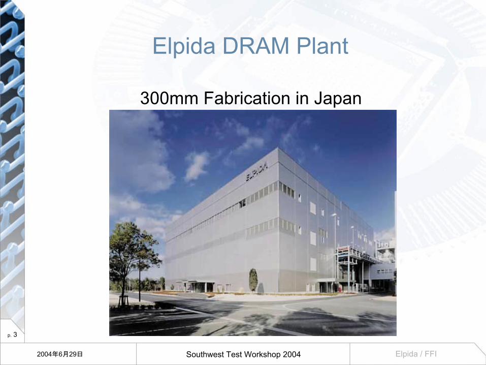
Elpida DRAM Plant
300mm Fabrication in Japan
p. 4
Southwest Test Workshop 20042004年6月29日 Elpida / FFI
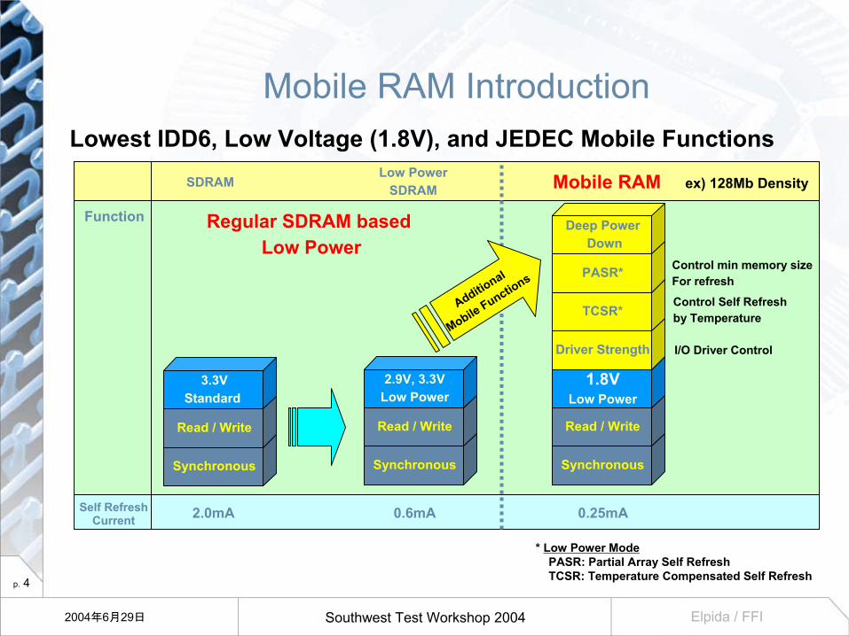
Lowest IDD6, Low Voltage (1.8V), and JEDEC Mobile Functions
* Low Power ModePASR: Partial Array Self RefreshTCSR: Temperature Compensated Self Refresh
Function
Synchronous Synchronous
Read / WriteRead / Write
SDRAM Mobile RAM
I/O Driver Control
Control Self Refresh by Temperature
Control min memory size For refresh
Synchronous
Read / Write
Low PowerSDRAM
Self RefreshCurrent
3.3VStandard
2.9V, 3.3VLow Power
1.8VLow Power
Driver Strength
TCSR*
PASR*
Deep PowerDown
ex) 128Mb Density
Additional
Mobile Functions
Regular SDRAM based Low Power
2.0mA 0.6mA 0.25mA
Mobile RAM Introduction
p. 5
Southwest Test Workshop 20042004年6月29日 Elpida / FFI
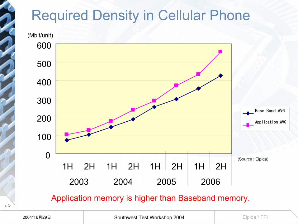
Required Density in Cellular Phone
Base Band AVG
Application AVG
(Mbit/unit)
(Source : Elpida)0
100
200
300
400
500
600
1H 2H 1H 2H 1H 2H 1H 2H
2003 2004 2005 2006
Application memory is higher than Baseband memory.
p. 6
Southwest Test Workshop 20042004年6月29日 Elpida / FFI
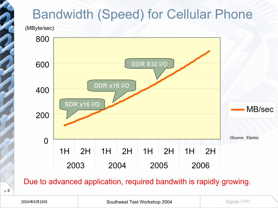
Bandwidth (Speed) for Cellular Phone
(Source : Elpida)
MB/sec
(MByte/sec)
0
200
400
600
800
1H 2H 1H 2H 1H 2H 1H 2H
2003 2004 2005 2006
DDR x16 I/O
DDR X32 I/O
SDR x16 I/O
Due to advanced application, required bandwith is rapidly growing.
p. 7
Southwest Test Workshop 20042004年6月29日 Elpida / FFI
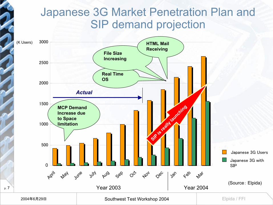
Japanese 3G Market Penetration Plan and SIP demand projection
0
500
1000
1500
2000
2500
3000
April
May
June Ju
ly
Aug Sep Oct
Nov Dec Jan
Feb Mar
Japanese 3G Users
Japanese 3G with SIP
Year 2003 Year 2004
(K Users)
MCP Demand Increase due to Space limitation
Real TimeOS
File Size Increasing
HTML Mail Receiving
SIP is re
ally l
aunch
ingActual
(Source: Elpida)

p. 8
Southwest Test Workshop 20042004年6月29日 Elpida / FFI
Mobile Memory TAM Trend
SDRAM
PSRAM
SRAM
1G SD
512M SD
256M SD
128M SD
64M SD
32M SD
Mobile SDRAM TAM
Memory TAM for Mobile Phone
2003 2004 2005 2006 2007
2003 2004 2005 2006 2007
p. 9
Southwest Test Workshop 20042004年6月29日 Elpida / FFI
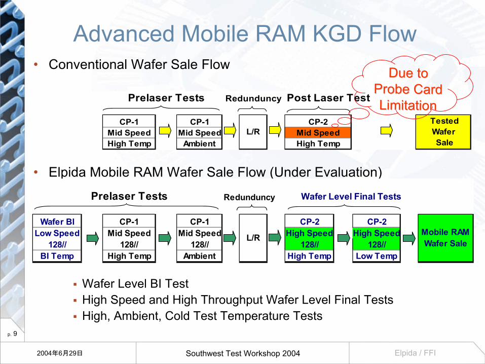
Advanced Mobile RAM KGD Flow• Conventional Wafer Sale Flow
• Elpida Mobile RAM Wafer Sale Flow (Under Evaluation)
Wafer Level BI TestHigh Speed and High Throughput Wafer Level Final TestsHigh, Ambient, Cold Test Temperature Tests
Prelaser Tests Redunduncy Post Laser Test
CP-1 CP-1Mid Speed Mid SpeedHigh Temp Ambient
L/RCP-2
Mid SpeedHigh Temp
TestedWafer Sale
Prelaser Tests Redunduncy
Wafer BI CP-1 CP-1 CP-2 CP-2Low Speed Mid Speed Mid Speed High Speed High Speed
128// 128// 128// 128// 128//BI Temp High Temp Ambient High Temp Low Temp
Mobile RAMWafer SaleL/R
Wafer Level Final Tests
Due to Due to Probe Card Probe Card LimitationLimitation
p. 10
Southwest Test Workshop 20042004年6月29日 Elpida / FFI
High Performance Probing Solution
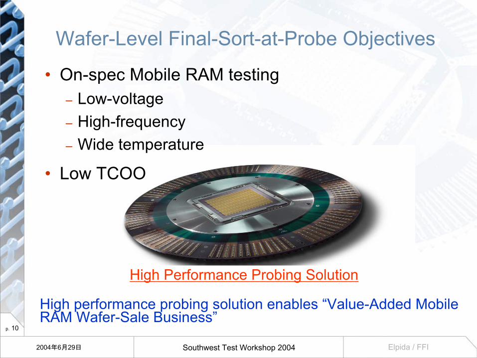
Wafer-Level Final-Sort-at-Probe Objectives
• On-spec Mobile RAM testing– Low-voltage– High-frequency– Wide temperature
• Low TCOO
High performance probing solution enables “Value-Added Mobile RAM Wafer-Sale Business”
p. 11
Southwest Test Workshop 20042004年6月29日 Elpida / FFI
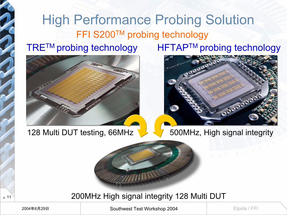
High Performance Probing Solution
TRETM probing technology HFTAPTM probing technologyFFI S200TM probing technology
128 Multi DUT testing, 66MHz 500MHz, High signal integrity
200MHz High signal integrity 128 Multi DUT
p. 12
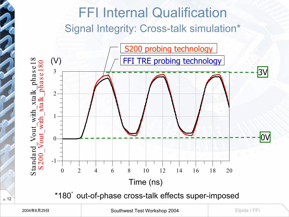
Southwest Test Workshop 20042004年6月29日 Elpida / FFI
2 4 6 8 10 12 14 16 180 20
0
1
2
-1
3
time, ns ec
S20
0_V
out_
with
_xta
lk_p
hase
180
Sta
ndar
d_V
out_
with
_xta
lk_p
hase
18
FFI Internal QualificationSignal Integrity: Cross-talk simulation*
S200 probing technologyFFI TRE probing technology
3V
0V
(V)
Time (ns)
*180°out-of-phase cross-talk effects super-imposed
p. 13
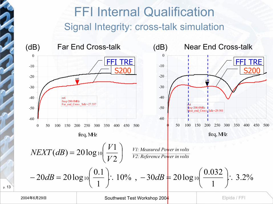
Southwest Test Workshop 20042004年6月29日 Elpida / FFI
m6freq=200.0MHzFar_end_Cross_Talk=-27.557
50 100 150 200 250 300 350 400 4500 500
-50
-40
-30
-20
-10
-60
0
freq, MHz
Far_
end_
Cro
ss_T
alk
m6
Far_
end_
Cro
ss_T
alk1
m4freq=200.0MHzNear_end_Cross_Talk=-29.501
50 100 150 200 250 300 350 400 4500 500
-50
-40
-30
-20
-10
-60
0
freq, MHz
Nea
r_en
d_C
ross
_Tal
k
m4
Nea
r_en
d_C
ross
_Tal
k2
Far End Cross-talk Near End Cross-talk(dB) (dB)
FFI Internal Qualification Signal Integrity: cross-talk simulation
%2.31032.0log2030 , %10
11.0log2020
21log20)(
1010
10
∴
=−∴
=−
=
dBdB
VVdBNEXT volts in Power Reference :V2
volts in Power Measured:V1
FFI TRES200
FFI TRES200

p. 14
Southwest Test Workshop 20042004年6月29日 Elpida / FFI
FFI Internal Qualification Signal Integrity: Tr/Tf Measurement
54 5652 58
0.2
0.3
0.1
0.4
time, nsec
U43
_A04
_V..C
HA
NN
EL2
m1
m2
$C_U
43_A
04_V
..CH
AN
NEL
2
m3
m4
t m1-m2 = 0.35nst m3-m4 = 0.45nsS200 Probing TechnologyFFI TRE Probing Technology
(V)
Time (ns)
S200 probing technology
FFI TRE probing technology
p. 15
Southwest Test Workshop 20042004年6月29日 Elpida / FFI
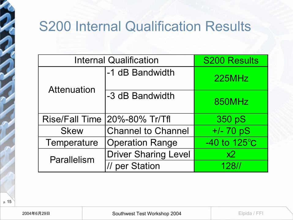
S200 Internal Qualification Results
S200 Results-1 dB Bandwidth 225MHz
-3 dB Bandwidth 850MHz
Rise/Fall Time 20%-80% Tr/Tfl 350 pSSkew Channel to Channel +/- 70 pS
Temperature Operation Range -40 to 125℃Driver Sharing Level x2// per Station 128//
Internal Qualification
Attenuation
Parallelism
p. 16
Southwest Test Workshop 20042004年6月29日 Elpida / FFI
• 143MHz tester + 100MHz Mobile RAM– Output pin waveform – DQ signal skew – Input and output voltage margins– Vcc margin– Timing margin – Wafer-to-wafer high-speed binning correlation
Wafer-Level Final-Sort Test Customer Qualification
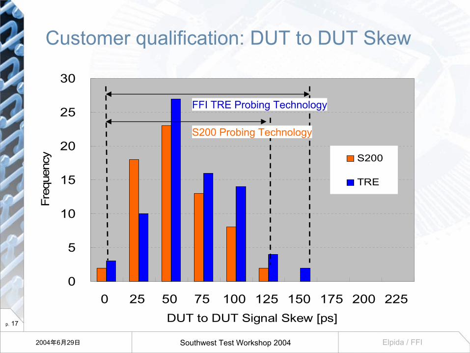
p. 17
Southwest Test Workshop 20042004年6月29日 Elpida / FFI
0
5
10
15
20
25
30
0 25 50 75 100 125 150 175 200 225DUT to DUT Signal Skew [ps]
Freq
uenc
y S200
TRE
Customer qualification: DUT to DUT Skew
S200 Probing Technology
FFI TRE Probing Technology
p. 18
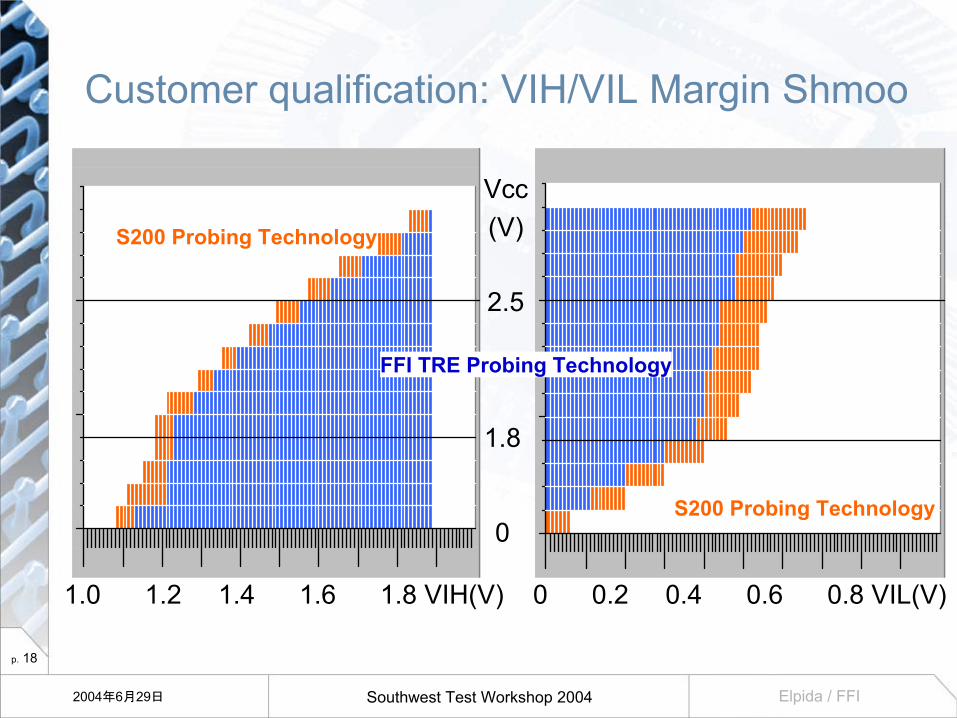
Southwest Test Workshop 20042004年6月29日 Elpida / FFI
Customer qualification: VIH/VIL Margin Shmoo
0
1.8
2.5
Vcc(V)
1.0 1.2 1.4 1.6 1.8 VIH(V) 0 0.2 0.4 0.6 0.8 VIL(V)
S200 Probing Technology
FFI TRE Probing Technology
S200 Probing Technology
p. 19
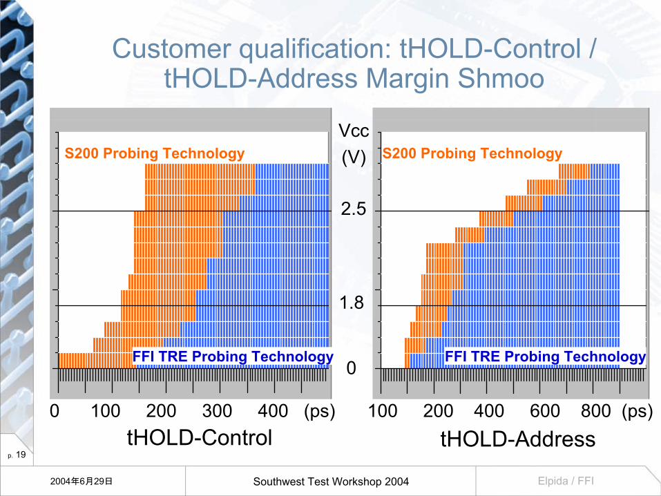
Southwest Test Workshop 20042004年6月29日 Elpida / FFI
Customer qualification: tHOLD-Control / tHOLD-Address Margin Shmoo
0
1.8
2.5
Vcc(V)
0 100 200 300 400 (ps) 100 200 400 600 800 (ps)tHOLD-Control tHOLD-Address
S200 Probing Technology S200 Probing Technology
FFI TRE Probing TechnologyFFI TRE Probing Technology
p. 20
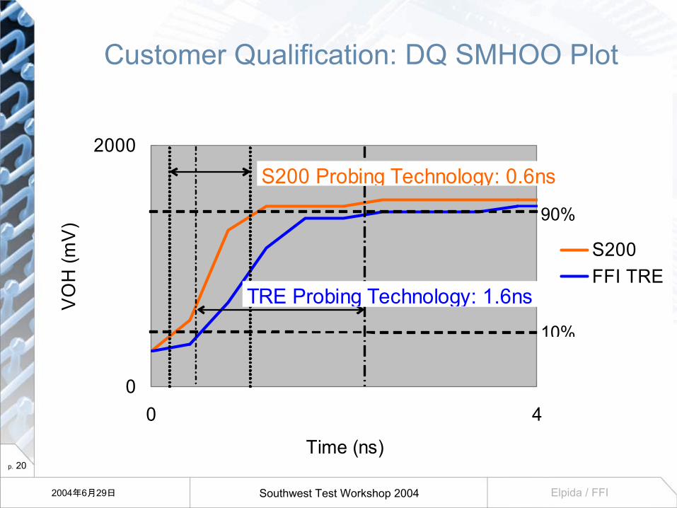
Southwest Test Workshop 20042004年6月29日 Elpida / FFI
0
2000
0 4
Time (ns)
VO
H (m
V)
S200FFI TRE
S200 Probing Technology: 0.6ns
TRE Probing Technology: 1.6ns
90%
10%
Customer Qualification: DQ SMHOO Plot
p. 21
Southwest Test Workshop 20042004年6月29日 Elpida / FFI
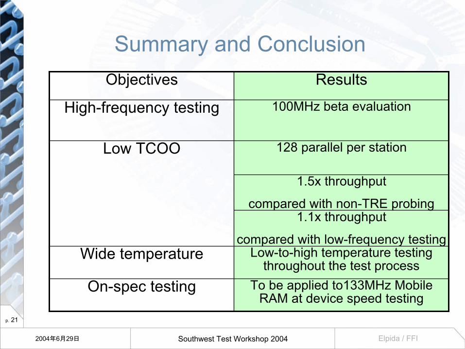
Summary and Conclusion
Low-to-high temperature testing throughout the test process
Wide temperature
To be applied to133MHz Mobile RAM at device speed testing
On-spec testing
1.1x throughput
compared with low-frequency testing
1.5x throughput
compared with non-TRE probing
128 parallel per stationLow TCOO
100MHz beta evaluationHigh-frequency testing
ResultsObjectives
p. 22
Southwest Test Workshop 20042004年6月29日 Elpida / FFI
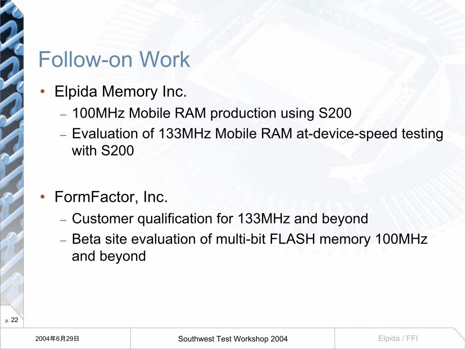
Follow-on Work• Elpida Memory Inc.
– 100MHz Mobile RAM production using S200 – Evaluation of 133MHz Mobile RAM at-device-speed testing
with S200
• FormFactor, Inc.– Customer qualification for 133MHz and beyond– Beta site evaluation of multi-bit FLASH memory 100MHz
and beyond
p. 23
Southwest Test Workshop 20042004年6月29日 Elpida / FFI
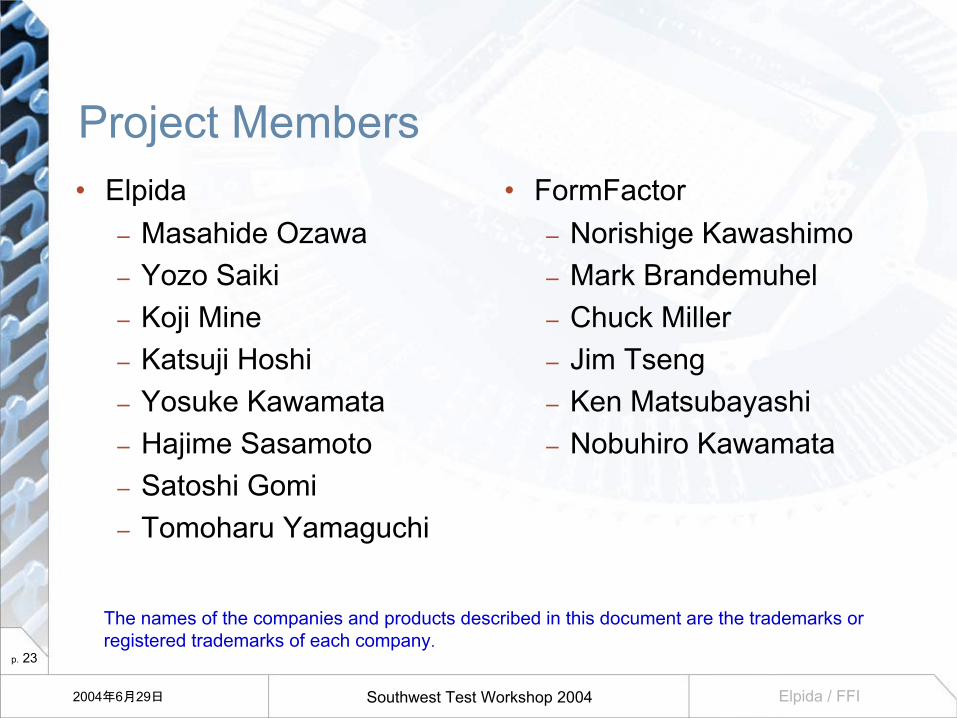
• Elpida– Masahide Ozawa– Yozo Saiki– Koji Mine– Katsuji Hoshi– Yosuke Kawamata– Hajime Sasamoto– Satoshi Gomi– Tomoharu Yamaguchi
• FormFactor– Norishige Kawashimo– Mark Brandemuhel– Chuck Miller – Jim Tseng– Ken Matsubayashi– Nobuhiro Kawamata
Project Members
The names of the companies and products described in this document are the trademarks or registered trademarks of each company.