Embed Size (px)
Citation preview

8/13/2019 DesktopTL 061CP2
http://slidepdf.com/reader/full/desktoptl-061cp2 1/36
SLOS078J − NOVEMBER 1978 − REVISED SEPTEMBER 2004
1POST OFFICE BOX 655303 • DALLAS, TEXAS 75265
Very Low Power Consumption
Typical Supply Current . . . 200 µA
(Per Amplifier)
Wide Common-Mode and Differential
Voltage Ranges
Low Input Bias and Offset Currents Common-Mode Input Voltage Range
Includes VCC+
Output Short-Circuit Protection
High Input Impedance . . . JFET-Input Stage
Internal Frequency Compensation
Latch-Up-Free Operation
High Slew Rate . . . 3.5 V/µs Typ
1
2
3
4
8
7
6
5
OFFSET N1
IN−
IN+
VCC−
NC
VCC+
OUT
OFFSET N2
TL061, TL061A . . . D, P, OR PS PACKAGE
TL061B . . . P PACKAGE
(TOP VIEW)
1
2
3
4
8
7
6
5
1OUT
1IN−
1IN+
VCC−
VCC+
2OUT
2IN−
2IN+
TL062 . . . D, JG, P, PS, OR PW PACKAGE
TL062A . . . D, P, OR PS PACKAGE
TL062B . . . D OR P PACKAGE
(TOP VIEW)
1
2
3
4
5
6
7
14
13
12
11
10
9
8
1OUT
1IN−
1IN+
VCC+
2IN+
2IN−
2OUT
4OUT
4IN−
4IN+
VCC−
3IN+
3IN−
3OUT
TL064 . . . D, J, N, NS, PW, OR W PACKAGE
TL064A, TL064B . . . D OR N PACKAGE
(TOP VIEW)
NC − No internal connection
NC
2OUT
NC
2IN−
NC
3 2 1 20 19
9 10 11 12 13
4
5
6
7
8
18
17
16
15
14
NC
1IN−
NC
1IN+
NC
TL062 . . . FK PACKAGE
(TOP VIEW)
N C
1 O U T
N C
2 I N + N C
N C
N C
N C
V C C −
V C C +
3 2 1 20 19
9 10 11 12 13
4
5
6
7
8
18
17
16
15
14
4IN+
NC
VCC−
NC
3IN+
1IN+
NC
VCC+
NC
2IN+
1 I N −
1 O U T
N C
3 O U T
3 I N −
4 O U T
4 I N −
2 I N −
2 O U T
N C
TL064 . . . FK PACKAGE
(TOP VIEW)
description/ordering information
The JFET-input operational amplifiers of the TL06_ series are designed as low-power versions of the
TL08_ series amplifiers. They feature high input impedance, wide bandwidth, high slew rate, and low input offsetand input bias currents. The TL06_ series features the same terminal assignments as the TL07_ andTL08_ series. Each of these JFET-input operational amplifiers incorporates well-matched, high-voltage JFETand bipolar transistors in an integrated circuit.
The C-suffix devices are characterized for operation from 0°C to 70°C. The I-suffix devices are characterized
for operation from −40°C to 85°C, and the M-suffix devices are characterized for operation over the full militarytemperature range of −55°C to 125°C.
Please be aware that an important notice concerning availability, standard warranty, and use in critical applications of
Texas Instruments semiconductor products and disclaimers thereto appears at the end of this data sheet.
Copyright© 2004, Texas Instruments Incorporated

8/13/2019 DesktopTL 061CP2
http://slidepdf.com/reader/full/desktoptl-061cp2 2/36
SLOS078J − NOVEMBER 1978 − REVISED SEPTEMBER 2004
2 POST OFFICE BOX 655303 • DALLAS, TEXAS 75265
description/ordering information (continued)
ORDERING INFORMATION
TAVIOMAX
AT 25°CPACKAGE† ORDERABLE
PART NUMBER
TOP-SIDE
MARKING
TL061CP TL061CP
PDIP (P) Tube of 50TL062CP TL062CP
PDIP (N) Tube of 25 TL064CN TL064CN
Tube of 75 TL061CD
Reel of 2500 TL061CDRTL061C
Tube of 75 TL062CD
SOIC (D)Reel of 2500 TL062CDR
TL062C
Tube of 50 TL064CD
15 mVReel of 2500 TL064CDR
TL064C
TL061CPSR T061
SOP (PS) Reel of 2000TL062CPSR T062
SOP (NS) Reel of 2000 TL064CNSR TL064
Tube of 150 TL062CPW
Reel of 2000 TL062CPWR
T062
TSSOP (PW)Tube of 90 TL064CPW
Reel of 2000 TL064CPWRT064
° ° TL061ACP TL061ACP
0°C to 70°C PDIP (P) Tube of 50TL062ACP TL062ACP
PDIP (N) Tube of 25 TL064ACN TL064ACN
Tube of 75 TL061ACD
Reel of 2500 TL061ACDR061AC
6 mV
Tube of 75 TL062ACDSOIC (D)
Reel of 2500 TL062ACDR062AC
Tube of 50 TL064ACD
Reel of 2500 TL064ACDRTL064AC
TL061ACPSR T061A
SOP (PS) Reel of 2000TL062ACPSR T062A
TL061BCP TL061BCP
PDIP (P) Tube of 50TL062BCP TL062BCP
PDIP (N) Tube of 25 TL064BCN TL064BCN
3 mV Tube of 75 TL062BCD
Reel of 2500 TL062BCDR
062BC
SOIC (D)Tube of 50 TL064BCD
Reel of 2500 TL064BCDRTL064BC
† Package drawings, standard packing quantities, thermal data, symbolization, and PCB design guidelines are available at
www.ti.com/sc/package.

8/13/2019 DesktopTL 061CP2
http://slidepdf.com/reader/full/desktoptl-061cp2 3/36
SLOS078J − NOVEMBER 1978 − REVISED SEPTEMBER 2004
3POST OFFICE BOX 655303 • DALLAS, TEXAS 75265
description/ordering information (continued)
ORDERING INFORMATION (continued)
TAVIOMAX
AT 25°CPACKAGE† ORDERABLE
PART NUMBER
TOP-SIDE
MARKING
TL061IP TL061IP
PDIP (P) Tube of 50TL062IP TL062IP
PDIP (N) Tube of 25 TL064IN TL064IN
Tube of 75 TL061ID
Reel of 2000 TL061IDR
TL061I
−40°C to 85°C 6 mV
Tube of 75 TL062ID
SOIC (D)Reel of 2000 TL062IDR
TL062I
Tube of 50 TL064ID
Reel of 2500 TL064IDRTL064I
TSSOP (PW) Reel of 2000 TL062IPWR TL062I
CDIP (JG) Tube of 50 TL062MJG TL062MJG
6 mVLCCC (FK) Tube of 55 TL062MFK TL062MFK
−55°C to 125°C CDIP (J) Tube of 25 TL064MJ TL064MJ
9 mV CFP (W) Tube of 150 TL064MW TL064MW
LCCC (FK) Tube of 55 TL064MFK TL064MFK
† Package drawings, standard packing quantities, thermal data, symbolization, and PCB design guidelines are available at
www.ti.com/sc/package.

8/13/2019 DesktopTL 061CP2
http://slidepdf.com/reader/full/desktoptl-061cp2 4/36
SLOS078J − NOVEMBER 1978 − REVISED SEPTEMBER 2004
4 POST OFFICE BOX 655303 • DALLAS, TEXAS 75265
symbol (each amplifier)
+
−
IN+
IN−OUT
OFFSET N1
Offset Null/Compensation
TL061 Only
OFFSET N2
schematic (each amplifier)
IN+
50 Ω
100 Ω
C1
VCC+
OUT VCC−OFFSET N1
TL061 Only
OFFSET N2
IN−
C1 = 10 pF on TL061, TL062, and TL064
Component values shown are nominal.

8/13/2019 DesktopTL 061CP2
http://slidepdf.com/reader/full/desktoptl-061cp2 5/36
SLOS078J − NOVEMBER 1978 − REVISED SEPTEMBER 2004
5POST OFFICE BOX 655303 • DALLAS, TEXAS 75265
absolute maximum ratings over operating free-air temperature range (unless otherwise noted)†
TL06_C
TL06_AC
TL06_BC
TL06_I TL06_M UNIT
Supply voltage, VCC+ (see Note 1) 18 18 18 V
Supply voltage, VCC−
(see Note 1) −18 −18 −18 V
Differential input voltage, VID (see Note 2) ±30 ±30 ±30 V
Input voltage, VI (see Notes 1 and 3) ±15 ±15 ±15 V
Duration of output short circuit (see Note 4) Unlimited Unlimited Unlimited
D (8-pin) package 97 97
D (14-pin) package 86 86
N package 80 80
NS package 76 76
Package thermal impedance, θJA (see Notes 5 and 6) P package 85 85 °C/W
PS package 95 95
PW (8-pin) package 149 149
PW (14-pin)
package113 113
FK package 5.61
J package 15.05
Package thermal impedance, θJC (see Notes 7 and 8)JG package 14.5
°C/W
W package 14.65
Operating virtual junction temperature, TJ 150 150 150 °C
Case temperature for 60 seconds FK package 260 °C
Lead temperature 1,6 mm (1/16 inch) from case for 60 J, JG, U, or ,
seconds
, , ,
W package300 °C
Lead temperature 1,6 mm (1/6 inch) from case for 10 D, N, NS, P, PS,°
,
seconds
, , , , ,
or PW package260 260 °C
Storage temperature range, Tstg −65 to 150 −65 to 150 −65 to 150 °C
† Stresses beyond those listed under “absolute maximum ratings” may cause permanent damage to the device. These are stress ratings only, and
functional operation of the device at these or any other conditions beyond those indicated under “recommended operating conditions” is not
implied. Exposure to absolute-maximum-rated conditions for extended periods may affect device reliability.
NOTES: 1. All voltage values except differential voltages are with respect to the midpoint between VCC+ and VCC−.
2. Differential voltages are at IN+ with respect to IN−.
3. The magnitude of the input voltage should never exceed the magnitude of the supply voltage or 15 V, whichever is less.
4. The output may be shorted to ground or to either supply. Temperature and/or supply voltages must be limited to ensure that the
dissipation rating is not exceeded.
5. Maximum power dissipation is a function of TJ(max), θJA, and TA. The maximum allowable power dissipation at any allowable
ambient temperature is PD = (TJ(max) − TA)/ θJA. Operating at the absolute maximum TJ of 150°C can affect reliability.
6. The package thermal impedance is calculated in accordance with JESD 51-7.
7. Maximum power dissipation is a function of TJ(max), θJC, and TC. The maximum allowable power dissipation at any allowable case
temperature is PD = (TJ(max) − TC)/ θJC. Operating at the absolute maximum TJ of 150°C can affect reliability.
8. The package thermal impedance is calculated in accordance with MIL-STD-883.

8/13/2019 DesktopTL 061CP2
http://slidepdf.com/reader/full/desktoptl-061cp2 6/36
SLOS078J − NOVEMBER 1978 − REVISED SEPTEMBER 2004
6 POST OFFICE BOX 655303 • DALLAS, TEXAS 75265
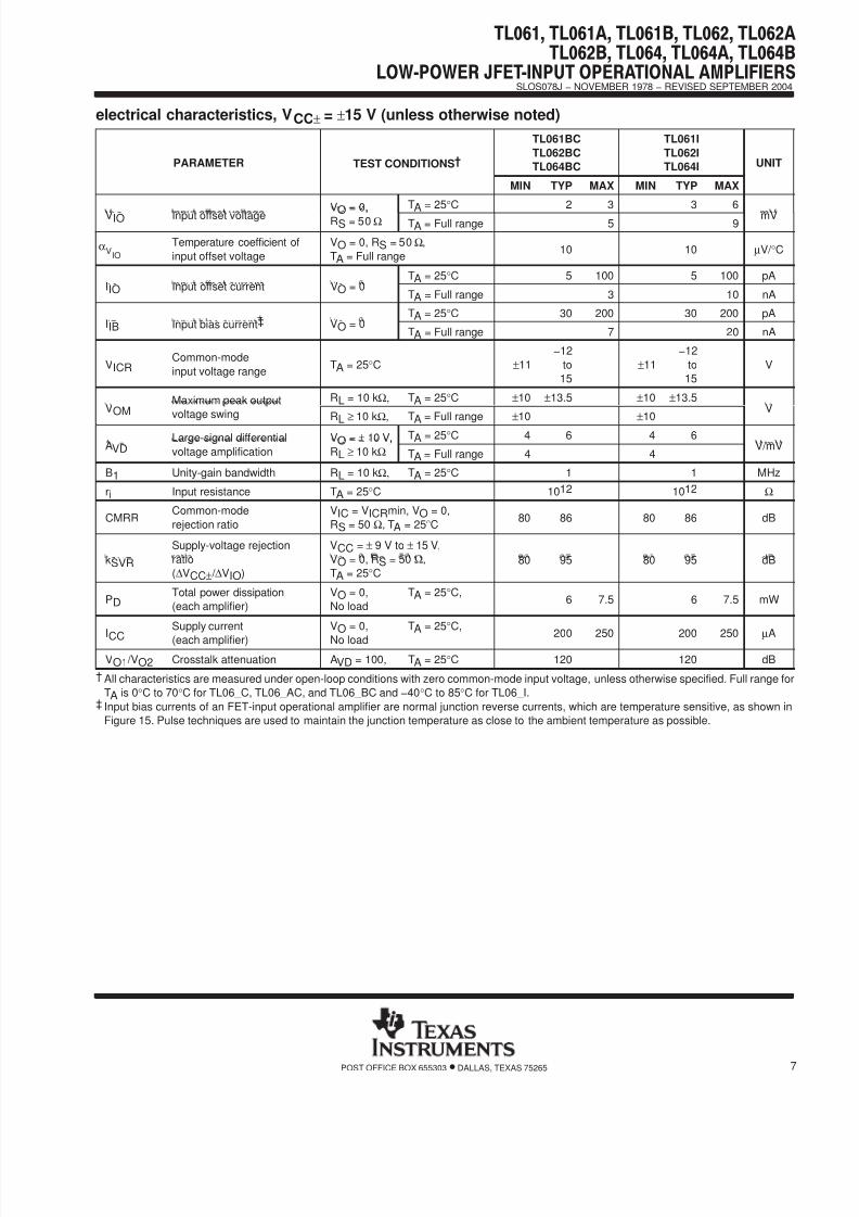
electrical characteristics, VCC± = ±15 V (unless otherwise noted)
PARAMETER TEST CONDITIONS†
TL061C
TL062C
TL064C
TL061AC
TL062AC
TL064AC UNIT
MIN TYP MAX MIN TYP MAX
VO = 0,TA
= 25°C 3 15 3 6VIO Input offset voltage ,RS = 50Ω TA = Full range 20 7.5
mV
αVIO
Temperature coefficient
of input offset voltage
VO = 0, RS = 50Ω,
TA = Full range10 10 µV/ °C
TA = 25°C 5 200 5 100 pA
IIO Input offset current VO = 0TA = Full range 5 3 nA
TA = 25°C 30 400 30 200 pA
IIB Input bias current‡ VO = 0TA = Full range 10 7 nA
Common-mode
−12 −12
VICR input voltage rangeTA = 25°C ±11 to
15±11 to
15V
Maximum peak output RL = 10 kΩ, TA = 25°C ±10 ±13.5 ±10 ±13.5VOM
voltage swing RL ≥ 10 kΩ, T
A = Full range ±10 ±10
V
Large-signal differential VO = ± 10 V, TA = 25°C 3 6 4 6AVD
voltage amplification
,
RL ≥ 10 kΩ TA = Full range 3 4V/mV
B1 Unity-gain bandwidth RL = 10 kΩ, TA = 25°C 1 1 MHz
ri Input resistance TA = 25°C 1012 1012 Ω
CMRRCommon-mode rejection
ratio
VIC = VICRmin, VO = 0,
RS = 50 Ω, TA = 25°C70 86 80 86 dB
Supply-voltage rejection VCC = ± 9 V to ± 15 V,
kSVR ratio
(∆VCC± / ∆VIO)
VO = 0, RS = 50 Ω,TA = 25°C
70 95 80 95 dB
PDTotal power dissipation
(each amplifier)
VO = 0,
No load
TA = 25°C,6 7.5 6 7.5 mW
ICC
Supply current
(each amplifier)
VO = 0,
No load
TA = 25°C,
200 250 200 250 µA
VO1 /VO2 Crosstalk attenuation AVD = 100, TA = 25°C 120 120 dB
† All characteristics are measured under open-loop conditions with zero common-mode input voltage unless otherwise specified. Full range for
TA is 0°C to 70°C for TL06_C, TL06_AC, and TL06_BC and −40°C to 85°C for TL06_I.‡ Input bias currents of an FET-input operational amplifier are normal junction reverse currents, which are temperature sensitive, as shown in
Figure 15. Pulse techniques are used to maintain the junction temperature as close to the ambient temperature as possible.
8/13/2019 DesktopTL 061CP2
http://slidepdf.com/reader/full/desktoptl-061cp2 7/36
SLOS078J − NOVEMBER 1978 − REVISED SEPTEMBER 2004
7POST OFFICE BOX 655303 • DALLAS, TEXAS 75265
electrical characteristics, VCC± = ±15 V (unless otherwise noted)
PARAMETER TEST CONDITIONS†
TL061BC
TL062BC
TL064BC
TL061I
TL062I
TL064I UNIT
MIN TYP MAX MIN TYP MAX
VO = 0,TA
= 25°C 2 3 3 6VIO Input offset voltage ,RS = 50Ω TA = Full range 5 9
mV
αVIO
Temperature coefficient of
input offset voltage
VO = 0, RS = 50Ω,
TA = Full range10 10 µV/ °C
TA = 25°C 5 100 5 100 pA
IIO Input offset current VO = 0TA = Full range 3 10 nA
TA = 25°C 30 200 30 200 pA
IIB Input bias current‡ VO = 0TA = Full range 7 20 nA
VICRCommon-mode
input voltage rangeTA = 25°C ±11
−12
to
15
±11
−12
to
15
V
Maximum peak output RL = 10 kΩ, TA = 25°C ±10 ±13.5 ±10 ±13.5VOM
voltage swing RL ≥ 10 kΩ, TA = Full range ±10 ±10V
Large-signal differential VO = ± 10 V, TA = 25°C 4 6 4 6AVD
voltage amplification
,
RL ≥ 10 kΩ TA = Full range 4 4V/mV
B1 Unity-gain bandwidth RL = 10 kΩ, TA = 25°C 1 1 MHz
ri Input resistance TA = 25°C 1012 1012 Ω
CMRRCommon-mode
rejection ratio
VIC = VICRmin, VO = 0,
RS = 50 Ω, TA = 25°C80 86 80 86 dB
Supply-voltage rejection VCC = ± 9 V to ± 15 V,
kSVR ratio
(∆VCC± / ∆VIO)
VO = 0, RS = 50 Ω,TA = 25°C
80 95 80 95 dB
PDTotal power dissipation
(each amplifier)
VO = 0,
No load
TA = 25°C,6 7.5 6 7.5 mW
ICC
Supply current
(each amplifier)
VO = 0,
No load
TA = 25°C,
200 250 200 250 µA
VO1 /VO2 Crosstalk attenuation AVD = 100, TA = 25°C 120 120 dB
† All characteristics are measured under open-loop conditions with zero common-mode input voltage, unless otherwise specified. Full range for
TA is 0°C to 70°C for TL06_C, TL06_AC, and TL06_BC and −40°C to 85°C for TL06_I.‡ Input bias currents of an FET-input operational amplifier are normal junction reverse currents, which are temperature sensitive, as shown in
Figure 15. Pulse techniques are used to maintain the junction temperature as close to the ambient temperature as possible.

8/13/2019 DesktopTL 061CP2
http://slidepdf.com/reader/full/desktoptl-061cp2 8/36
SLOS078J − NOVEMBER 1978 − REVISED SEPTEMBER 2004
8 POST OFFICE BOX 655303 • DALLAS, TEXAS 75265
electrical characteristics, VCC± = ±15 V (unless otherwise noted)
PARAMETER TEST CONDITIONS†
TL061M
TL062MTL064M
UNIT
MIN TYP MAX MIN TYP MAX
VO = 0, TA = 25°C 3 6 3 9
VIO Input offset voltage ,
RS = 50Ω TA = −55°C to 125°C 9 15
mV
αVIO
Temperature coefficient
of input offset voltage
VO = 0, RS = 50Ω,
TA = −55°C to 125°C10 10 µV/ °C
TA = 25°C 5 100 5 100 pA
IIO Input offset current VO = 0 TA = −55°C 20* 20*
TA = 125°C 20 20nA
TA = 25°C 30 200 30 200 pA
IIB Input bias current‡ VO = 0 TA = −55°C 50* 50*
TA = 125°C 50 50nA
VICRCommon-mode
input voltage rangeTA = 25°C ±11.5
−12
to
15±11.5
−12
to
15
V
Maximum peak output RL = 10 kΩ, TA = 25°C ±10 ±13.5 ±10 ±13.5VOM voltage swing RL ≥ 10 kΩ, TA = −55°C to 125°C ±10 ±10
V
Large-signal differentialVO = ±10 V, TA = 25°C 4 6 4 6
AVDvoltage amplification
,
RL ≥ 10 kΩ TA = −55°C to 125°C 4 4V/mV
B1 Unity-gain bandwidth RL = 10 kΩ, TA = 25°C MHz
ri Input resistance TA = 25°C 1012 1012 Ω
CMRRCommon-mode
rejection ratio
VIC = VICRmin, VO = 0,
RS = 50Ω, TA = 25°C80 86 80 86 dB
kSVR
Supply-voltage
rejection
ratio (∆VCC± / ∆VIO)
VCC = ±9 V to ±15 V, VO = 0,
RS = 50Ω, TA = 25°C80 95 80 95 dB
PD
Total power dissipation
(each amplifier)
VO = 0,
No load
TA = 25°C,
6 7.5 6 7.5 mW
ICCSupply current
(each amplifier)
VO = 0,
No load
TA = 25°C,200 250 200 250 µA
VO1 /VO2 Crosstalk attenuation AVD = 100, TA = 25°C 120 120 dB
* This parameter is not production tested.† All characteristics are measured under open-loop conditions, with zero common-mode voltage, unless otherwise specified.‡ Input bias currents of an FET-input operational amplifier are normal junction reverse currents, which are temperature sensitive, as shown in
Figure 15. Pulse techniques are used to maintain the junction temperature as close to the ambient temperature as possible.
operating characteristics, VCC± = ±15 V, TA = 25°C
PARAMETER TEST CONDITIONS MIN TYP MAX UNIT
SR Slew rate at unity gain (see Note 5)VI = 10 V,
RL
= 10 kΩ,CL = 100 pF,
See Figure 11.5 3.5 V/ µs
tr Rise time VI = 20 mV, RL = 10 kΩ, 0.2
Overshoot factor
,
CL = 100 pF,
,See Figure 1 10%
µs
Vn Equivalent input noise voltage RS = 20 Ω, f = 1 kHz 42 nV/ √Hz
NOTE 5: Slew rate at −55°C to 125°C is 0.7 V/ µs min.
8/13/2019 DesktopTL 061CP2
http://slidepdf.com/reader/full/desktoptl-061cp2 9/36
SLOS078J − NOVEMBER 1978 − REVISED SEPTEMBER 2004
9POST OFFICE BOX 655303 • DALLAS, TEXAS 75265
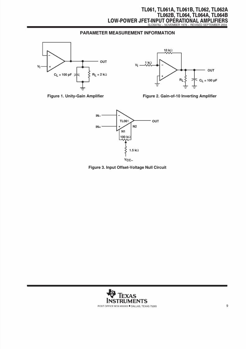
PARAMETER MEASUREMENT INFORMATION
VI
RL = 2 kΩ
+
−
CL = 100 pF
OUT
Figure 1. Unity-Gain Amplifier
VI
10 kΩ
1 kΩ
RL CL = 100 pF
+
−
OUT
Figure 2. Gain-of-10 Inverting Amplifier
N2
N1
100 kΩ
1.5 kΩ
VCC−
+
−
TL061
IN−
OUTIN+
Figure 3. Input Offset-Voltage Null Circuit

8/13/2019 DesktopTL 061CP2
http://slidepdf.com/reader/full/desktoptl-061cp2 10/36
SLOS078J − NOVEMBER 1978 − REVISED SEPTEMBER 2004
10 POST OFFICE BOX 655303 • DALLAS, TEXAS 75265
TYPICAL CHARACTERISTICS
Table of Graphs
FIGURE
Maximum peak output voltage vs Supply voltage 4
Maximum peak output voltage vs Free-air temperature 5
Maximum peak output voltage vs Load resistance 6
Maximum peak output voltage vs Frequency 7
Differential voltage amplification vs Free-air temperature 8
Large-signal differential voltage amplification vs Frequency 9
Phase shift vs Frequency 9
Supply current vs Supply voltage 10
Supply current vs Free-air temperature 11
Total power dissipation vs Free-air temperature 12
Common-mode rejection ratio vs Free-air temperature 13
Normalized unity-gain bandwidth vs Free-air temperature 14
Normalized slew rate vs Free-air temperature 14
Normalized phase shift vs Free-air temperature 14
Input bias current vs Free-air temperature 15
Voltage-follower large-signal pulse response vs Time 16
Output voltage vs Elapsed time 17
Equivalent input noise voltage vs Frequency 18

8/13/2019 DesktopTL 061CP2
http://slidepdf.com/reader/full/desktoptl-061cp2 11/36
SLOS078J − NOVEMBER 1978 − REVISED SEPTEMBER 2004
11POST OFFICE BOX 655303 • DALLAS, TEXAS 75265
TYPICAL CHARACTERISTICS†
Figure 4
00
− M a x i m u m
P e a k O u t p u t V o l t a g e − V
|VCC±| − Supply Voltage − V
±2.5
±5
±7.5
±10
±12.5
±15
2 4 6 8 10 12 14 16
RL = 10 kΩTA = 25°CSee Figure 2
MAXIMUM PEAK OUTPUT VOLTAGE
vs
SUPPLY VOLTAGE
Á Á
Á Á
V O M
Figure 5
−750
TA − Free-Air Temperature − °C
±2.5
±5
±7.5
±10
±12.5
±15
−50 −25 0 25 50 75 100 125
VCC± = ±15 VRL = 10 kΩSee Figure 2
MAXIMUM PEAK OUTPUT VOLTAGE
vs
FREE-AIR TEMPERATURE
− M a x i m u m P e a k O u t p u t V o l t a g e − V
Á Á
Á Á
V O M
Figure 6
See Figure 2TA = 25°C
VCC± = ±15 V
0100
RL − Load Resistance − Ω
1 k 10 k
±2.5
±5
±7.5
±10
±12.5
±15
200 400 700 2 k 4 k 7 k
MAXIMUM PEAK OUTPUT VOLTAGE
vs
LOAD RESISTANCE
− M a x i m u m P e a k O u t p u t V o l t a g e −
V
Á Á
Á Á
V O M
VCC± = ±12 V
VCC± = ±5 V
f − Frequency − Hz
1 k0
10 k 100 k 1 M 10 M
±2.5
±5
±7.5
±10
±12.5
±15
MAXIMUM PEAK OUTPUT VOLTAGE
vs
FREQUENCY
Á Á Á Á
Á Á Á Á
Á Á Á Á
Á Á Á Á
RL = 10 kΩ
TA = 25°CSee Figure 2
Á Á Á Á Á
Á Á Á Á Á
VCC± = ±15 V
Figure 7
− M a x i m u m P e a k O u t p u t V o l t a g e −
V
Á Á
Á Á
V O M
† Data at high and low temperatures are applicable only within the specified operating free-air temperature ranges of the various devices.

8/13/2019 DesktopTL 061CP2
http://slidepdf.com/reader/full/desktoptl-061cp2 12/36
SLOS078J − NOVEMBER 1978 − REVISED SEPTEMBER 2004
12 POST OFFICE BOX 655303 • DALLAS, TEXAS 75265
TYPICAL CHARACTERISTICS†
−
D i f f e r e n t i a l V o l t a g e A m p l i f i c a t i o n − V / m V
A V D
RL = 10 kΩVCC± = ±15 V
1−75
TA − Free-Air Temperature − °C
−50 −25 0 25 50 75 100 125
2
4
10
7
DIFFERENTIAL VOLTAGE AMPLIFICATION
vs
FREE-AIR TEMPERATURE
Figure 8
AVD
(left scale)
10.001
f − Frequency − Hz
10 100 1 k 10 k 100 k 1 M 10 M
0.01
0.1
1
10
100
P h a s e S h i f t
135°
90°
180°
45°
0°
VCC± = ±15 V
Rext = 0
RL = 10 kΩTA = 25°C
Phase Shift
(right scale)
LARGE-SIGNAL
DIFFERENTIAL VOLTAGE
AMPLIFICATION AND PHASE SHIFT
vs
FREQUENCY
− L a r g e - S i g n a l D i f f e r e n t i a l
A V D
V o l t a g e A m p l i f i c a t i o n − V / m V
Figure 9† Data at high and low temperatures are applicable only within the specified operating free-air temperature ranges of the various devices.

8/13/2019 DesktopTL 061CP2
http://slidepdf.com/reader/full/desktoptl-061cp2 13/36
SLOS078J − NOVEMBER 1978 − REVISED SEPTEMBER 2004
13POST OFFICE BOX 655303 • DALLAS, TEXAS 75265
TYPICAL CHARACTERISTICS†
Figure 10
TA = 25°CNo Signal
No Load
00
2 4 6 8 10 12 14 16
50
100
150
200
250
SUPPLY CURRENT
vs
SUPPLY VOLTAGE
|VCC±| − Supply Voltage − V
I C C − S u p p l y C u r r e n t − µ A
Á Á
Á Á
Á Á
I C C ±
I C C − S u p p l y C u r r e n t − µ A
Figure 11
−750
TA − Free-Air Temperature − °C
50
100
150
200
250
−50 −25 0 25 50 75 100 125
SUPPLY CURRENT
vs
FREE-AIR TEMPERATURE
Á Á
Á Á
Á Á
I C C ±
Î Î Î Î Î Î
Î Î Î Î Î Î
Î Î Î Î Î Î
VCC± = ±15 VNo Signal
No Load
Figure 12
−750
TA − Free-Air Temperature − °C
5
10
15
20
25
30
−50 −25 0 25 50 75 100 125
VCC± = ±15 V
No Signal
No Load
TL064
TL062
TL061
TOTAL POWER DISSIPATION
vs
FREE-AIR TEMPERATURE
P D − T o t a l P o w e r D i s s i p a t i o n − m W
Á Á
Á Á
P D
Figure 13
81
C M R
R − C o m m o n - M o d e R e j e c t i o n R a t i o − d B
1251007550250−25−50
TA − Free-Air Temperature − °C
−75
82
83
84
85
86
87
VCC± = ±15 VRL = 10 kΩ
ALL EXCEPT TL06_C
COMMON-MODE REJECTION RATIO
vs
FREE-AIR TEMPERATURE
† Data at high and low temperatures are applicable only within the specified operating free-air temperature ranges of the various devices.

8/13/2019 DesktopTL 061CP2
http://slidepdf.com/reader/full/desktoptl-061cp2 14/36
SLOS078J − NOVEMBER 1978 − REVISED SEPTEMBER 2004
14 POST OFFICE BOX 655303 • DALLAS, TEXAS 75265
TYPICAL CHARACTERISTICS
0.7 N o r m a l i z e d U n i t y - G a i n B a n d w i d t h a n d S l e w R a t e
1251007550250−25−50
TA − Free-Air Temperature − °C−75
0.8
0.9
1
1.1
1.2
1.3
1.02
1.01
1
0.99
0.98
0.97
N o r m a l i z e d P h a s e S h i f t
1.03
VCC± = ±15 VRL = 10 kΩf = B1 for Phase Shift
Unity-Gain Bandwidth
(left scale)Phase Shift
(right scale)
Slew Rate
(left scale)
NORMALIZED UNITY-GAIN BANDWIDTH,
SLEW RATE, AND PHASE SHIFT
vs
FREE-AIR TEMPERATURE
Figure 14
1251007550250−250.01
I I B − I n p u t B i a s C u r r e n t − n A
−50
TA − Free-Air Temperature − °C
0.04
0.1
0.4
1
4
10
40
100
INPUT BIAS CURRENT
vs
FREE-AIR TEMPERATURE
Á Á Á Á Á
VCC± = ±15 V
Á Á
Á Á
I I B
Figure 15 Figure 16
−6
I n p u t a n d O u t p u t V o l t a g e s − V
t − Time − µs
Input
Output
VCC± = ±15 V
RL = 10 kΩCL = 100 pF
TA = 25°C
0 2 4 6 8 10
−4
−2
0
2
4
6
VOLTAGE-FOLLOWER
LARGE-SIGNAL PULSE RESPONSE
vs
TIME

8/13/2019 DesktopTL 061CP2
http://slidepdf.com/reader/full/desktoptl-061cp2 15/36
SLOS078J − NOVEMBER 1978 − REVISED SEPTEMBER 2004
15POST OFFICE BOX 655303 • DALLAS, TEXAS 75265
TYPICAL CHARACTERISTICS
Figure 17
−4
− O u t p u t V o l t a g e − m V
t − Elapsed Time − µs
0 0.2 0.4 0.6 0.8 1 1.2 1.4
0
4
8
12
16
20
24
28
VCC± = ±15 V
RL = 10 kΩTA = 25°C
10%
tr
Overshoot
90%
OUTPUT VOLTAGE
vs
ELAPSED TIME
V O
Á Á
Á Á
V n
0
− E q
u i v a l e n t I n p u t N o i s e V o l t a g e −
f − Frequency − Hz
10
20
30
40
50
60
70
80
90
100
10 40 100 400 1 k 4 k 10 k 40 k 100 k
EQUIVALENT INPUT NOISE VOLTAGE
vs
FREQUENCY
Á Á Á Á Á
Á Á Á Á Á
Á Á Á Á Á
VCC± = ±15 VRS = 20 ΩTA = 25°C
n V /
H z
Figure 18

8/13/2019 DesktopTL 061CP2
http://slidepdf.com/reader/full/desktoptl-061cp2 16/36
SLOS078J − NOVEMBER 1978 − REVISED SEPTEMBER 2004
16 POST OFFICE BOX 655303 • DALLAS, TEXAS 75265
APPLICATION INFORMATION
Table of Application Diagrams
APPLICATION DIAGRAMPART
NUMBERFIGURE
Instrumentation amplifier TL064 190.5-Hz square-wave oscillator TL061 20
High-Q notch filter TL061 21
Audio-distribution amplifier TL064 22
Low-level light detector preamplifier TL061 23
AC amplifier TL061 24
Microphone preamplifier with tone control TL061 25
Instrumentation amplifier TL062 26
IC preamplifier TL062 27
+
−
−
+
+
− +
−
TL064
VCC+
VCC−
100 kΩInput B
10 kΩ0.1% 0.1%10 kΩ
VCC−
VCC+
TL064
Input A
VCC+
TL064
VCC−
100 kΩ
10 kΩ0.1%
10 kΩ0.1%
TL064
VCC−
VCC+
100 kΩ
100 kΩ
Output
1 MΩ
Figure 19. Instrumentation Amplifier
TL061 +
−
−15 V
15 V
Output
1 kΩ
9.1 kΩ3.3 kΩ
CF = 3.3 µF
RF = 100 kΩ
3.3 kΩ
f 1
2RFCF
Figure 20. 0.5-Hz Square-Wave Oscillator
TL061 +
−
R2
R1
C1 C2R3
C3 VCC−
VCC+
OutputInput
C1 C2 C32 110 pF
fo 1
2R1C1 1 kHz
R1 = R2 = 2 × R3 = 1.5 MΩ
Figure 21. High-Q Notch Filter

8/13/2019 DesktopTL 061CP2
http://slidepdf.com/reader/full/desktoptl-061cp2 17/36
SLOS078J − NOVEMBER 1978 − REVISED SEPTEMBER 2004
17POST OFFICE BOX 655303 • DALLAS, TEXAS 75265
APPLICATION INFORMATION
+
−
+
−
TL064 Output C
VCC+
VCC+
Output BTL064
−
+
VCC+
Output ATL064
−
+VCC+
TL064
VCC+100 kΩ
100 µF
Input
1 µF
1 MΩ
100 kΩ
100 kΩ
Figure 22. Audio-Distribution Amplifier
+
−
TIL601
10 kΩ
15 V
Output
−15 V
5 kΩ
100 pF TL061
10 kΩ
10 kΩ
10 kΩ
10 kΩ
10 kΩ
Figure 23. Low-Level Light Detector Preamplifier

8/13/2019 DesktopTL 061CP2
http://slidepdf.com/reader/full/desktoptl-061cp2 18/36
SLOS078J − NOVEMBER 1978 − REVISED SEPTEMBER 2004
18 POST OFFICE BOX 655303 • DALLAS, TEXAS 75265
APPLICATION INFORMATION
TL061
N2
+
−
0.1 µF
10 kΩ
50 Ω
250 kΩ
N1
Output
1 MΩ
VCC+
10 kΩ
10 kΩ
0.1 µF
Figure 24. AC Amplifier
1.2 MΩ 100 kΩ
20 µF
+
−
0.1 µF
47 kΩTL061
2.7 kΩ
270 Ω 0.003 µF 0.001 µF
0.002 µF
1 µF
10 kΩ
100 kΩ
50 kΩ
0.06 µF
50 kΩ
10 kΩ 100 kΩ 1 kΩ
0.06 µF
10 kΩ
0.02 µF
100 kΩ
+
Figure 25. Microphone Preamplifier With Tone Control
IN−
IN+
100 kΩ
TL062
TL062
1 kΩ
1 kΩ
100 kΩ
−
+
−
+
Output
Figure 26. Instrumentation Amplifier

8/13/2019 DesktopTL 061CP2
http://slidepdf.com/reader/full/desktoptl-061cp2 19/36
SLOS078J − NOVEMBER 1978 − REVISED SEPTEMBER 2004
19POST OFFICE BOX 655303 • DALLAS, TEXAS 75265
APPLICATION INFORMATION
TL062
220 kΩ
−
+
0.00375 µF
TL062
−
+
10 pF
68 kΩ
0.003 µF
0.03 µF
0.03 µF
10 kΩ 3.3 kΩ
0.003 µF
VCC−
VCC+
Output
Input
VCC−
VCC+
10 pF
MIN
MAX
100 kΩTreble
MIN
MAX
100 kΩBass
10 kΩ
10 kΩ
+
0.01 µF 27 kΩ
100 Ω
Balance
100 Ω
50 pF+
75 µF
47 µF
5 kΩGain
47 kΩ
1 µF
Á Á Á Á Á
Á Á Á Á Á
Á Á Á Á Á
TA = 25°CVCC± = ±15 V
Max
Treble
Max Bass
200 10 k4 k2 k1 k40040 100
20
15
10
5
0
−5
−10
−15
−20
−2520 k
25
f − Frequency − Hz
V o l t a g e A m p l i f i c a t i o n − d B
20
IC PREAMPLIFIER RESPONSE CHARACTERISTICS
Á Á Á
Á Á Á
Min
TrebleÁ Á Á
Á Á Á
Min Bass
Figure 27. IC Preamplifier

8/13/2019 DesktopTL 061CP2
http://slidepdf.com/reader/full/desktoptl-061cp2 20/36
PACKAGING INFORMATION
Orderable Device Status (1) PackageType
PackageDrawing
Pins PackageQty
Eco Plan (2) Lead/Ball Finish MSL Peak Temp (3)
81023012A OBSOLETE LCCC FK 20 None Call TI Call TI
81023022A ACTIVE LCCC FK 20 1 None POST-PLATE Level-NC-NC-NC
8102302HA ACTIVE CFP U 10 1 None A42 SNPB Level-NC-NC-NC
8102302PA ACTIVE CDIP JG 8 1 None A42 SNPB Level-NC-NC-NC
81023032A ACTIVE LCCC FK 20 1 None POST-PLATE Level-NC-NC-NC
8102303CA ACTIVE CDIP J 14 1 None A42 SNPB Level-NC-NC-NC
8102303DA ACTIVE CFP W 14 1 None A42 SNPB Level-NC-NC-NC
TL061ACD ACTIVE SOIC D 8 75 Pb-Free(RoHS)
CU NIPDAU Level-2-260C-1 YEAR/Level-1-235C-UNLIM
TL061ACDR ACTIVE SOIC D 8 2500 Pb-Free(RoHS)
CU NIPDAU Level-2-260C-1 YEAR/Level-1-235C-UNLIM
TL061ACP ACTIVE PDIP P 8 50 Pb-Free(RoHS)
CU NIPDAU Level-NC-NC-NC
TL061ACPSR ACTIVE SO PS 8 2000 Pb-Free(RoHS)
CU NIPDAU Level-2-260C-1 YEAR/Level-1-235C-UNLIM
TL061BCD OBSOLETE SOIC D 8 None Call TI Call TI
TL061BCP ACTIVE PDIP P 8 50 Pb-Free(RoHS)
CU NIPDAU Level-NC-NC-NC
TL061CD ACTIVE SOIC D 8 75 Pb-Free(RoHS)
CU NIPDAU Level-2-260C-1 YEAR/Level-1-235C-UNLIM
TL061CDR ACTIVE SOIC D 8 2500 Pb-Free(RoHS)
CU NIPDAU Level-2-260C-1 YEAR/Level-1-235C-UNLIM
TL061CP ACTIVE PDIP P 8 50 Pb-Free(RoHS)
CU NIPDAU Level-NC-NC-NC
TL061CPSR ACTIVE SO PS 8 2000 Pb-Free(RoHS)
CU NIPDAU Level-2-260C-1 YEAR/Level-1-235C-UNLIM
TL061CPWLE OBSOLETE TSSOP PW 8 None Call TI Call TI
TL061ID ACTIVE SOIC D 8 75 Pb-Free(RoHS)
CU NIPDAU Level-2-260C-1 YEAR/Level-1-235C-UNLIM
TL061IDR ACTIVE SOIC D 8 2500 Pb-Free(RoHS)
CU NIPDAU Level-2-260C-1 YEAR/Level-1-235C-UNLIM
TL061IP ACTIVE PDIP P 8 50 Pb-Free(RoHS)
CU NIPDAU Level-NC-NC-NC
TL061MJG OBSOLETE CDIP JG 8 None Call TI Call TI
TL061MJGB OBSOLETE CDIP JG 8 None Call TI Call TI
TL062ACD ACTIVE SOIC D 8 75 Pb-Free(RoHS)
CU NIPDAU Level-2-250C-1 YEAR
TL062ACDR ACTIVE SOIC D 8 2500 Pb-Free(RoHS)
CU NIPDAU Level-2-250C-1 YEAR
TL062ACJG OBSOLETE CDIP JG 8 None Call TI Call TI
TL062ACP ACTIVE PDIP P 8 50 Pb-Free(RoHS)
CU NIPDAU Level-NC-NC-NC
TL062ACPSR ACTIVE SO PS 8 2000 Pb-Free(RoHS)
CU NIPDAU Level-2-260C-1 YEAR/Level-1-235C-UNLIM
TL062BCD ACTIVE SOIC D 8 75 Pb-Free(RoHS)
CU NIPDAU Level-2-250C-1 YEAR
TL062BCDR ACTIVE SOIC D 8 2500 Pb-Free CU NIPDAU Level-2-250C-1 YEAR
PACKAGE OPTION ADDENDUM
www.ti.com 18-Feb-2005
Addendum-Page 1

8/13/2019 DesktopTL 061CP2
http://slidepdf.com/reader/full/desktoptl-061cp2 21/36
Orderable Device Status (1) PackageType
PackageDrawing
Pins PackageQty
Eco Plan (2) Lead/Ball Finish MSL Peak Temp (3)
(RoHS)
TL062BCP ACTIVE PDIP P 8 50 Pb-Free(RoHS)
CU NIPDAU Level-NC-NC-NC
TL062CD ACTIVE SOIC D 8 75 Pb-Free(RoHS)
CU NIPDAU Level-2-260C-1 YEAR/Level-1-235C-UNLIM
TL062CDR ACTIVE SOIC D 8 2500 Pb-Free(RoHS)
CU NIPDAU Level-2-260C-1 YEAR/Level-1-235C-UNLIM
TL062CJG OBSOLETE CDIP JG 8 None Call TI Call TI
TL062CP ACTIVE PDIP P 8 50 Pb-Free(RoHS)
CU NIPDAU Level-NC-NC-NC
TL062CPSLE OBSOLETE SO PS 8 None Call TI Call TI
TL062CPSR ACTIVE SO PS 8 2000 Pb-Free(RoHS)
CU NIPDAU Level-2-260C-1 YEAR/Level-1-235C-UNLIM
TL062CPW ACTIVE TSSOP PW 8 150 Pb-Free(RoHS)
CU NIPDAU Level-1-250C-UNLIM
TL062CPWLE OBSOLETE TSSOP PW 8 None Call TI Call TI
TL062CPWR ACTIVE TSSOP PW 8 2000 Pb-Free(RoHS)
CU NIPDAU Level-1-250C-UNLIM
TL062ID ACTIVE SOIC D 8 75 Pb-Free(RoHS)
CU NIPDAU Level-2-250C-1 YEAR
TL062IDR ACTIVE SOIC D 8 2500 Pb-Free(RoHS)
CU NIPDAU Level-2-250C-1 YEAR
TL062IJG OBSOLETE CDIP JG 8 None Call TI Call TI
TL062IP ACTIVE PDIP P 8 50 Pb-Free(RoHS)
CU NIPDAU Level-NC-NC-NC
TL062IPWR ACTIVE TSSOP PW 8 2000 Pb-Free(RoHS)
CU NIPDAU Level-1-250C-UNLIM
TL062MFKB ACTIVE LCCC FK 20 1 None POST-PLATE Level-NC-NC-NC
TL062MJG ACTIVE CDIP JG 8 1 None A42 SNPB Level-NC-NC-NC
TL062MJGB ACTIVE CDIP JG 8 1 None A42 SNPB Level-NC-NC-NC
TL064ACD ACTIVE SOIC D 14 50 Pb-Free(RoHS)
CU NIPDAU Level-2-250C-1 YEAR
TL064ACDR ACTIVE SOIC D 14 2500 Pb-Free(RoHS)
CU NIPDAU Level-2-250C-1 YEAR
TL064ACN ACTIVE PDIP N 14 25 Pb-Free(RoHS)
CU NIPDAU Level-NC-NC-NC
TL064BCD ACTIVE SOIC D 14 50 Pb-Free(RoHS)
CU NIPDAU Level-2-250C-1 YEAR
TL064BCDR ACTIVE SOIC D 14 2500 Pb-Free(RoHS)
CU NIPDAU Level-2-250C-1 YEAR
TL064BCN ACTIVE PDIP N 14 25 Pb-Free(RoHS)
CU NIPDAU Level-NC-NC-NC
TL064CD ACTIVE SOIC D 14 50 Pb-Free(RoHS) CU NIPDAU Level-2-260C-1 YEAR/Level-1-235C-UNLIM
TL064CDR ACTIVE SOIC D 14 2500 Pb-Free(RoHS)
CU NIPDAU Level-2-260C-1 YEAR/Level-1-235C-UNLIM
TL064CN ACTIVE PDIP N 14 25 Pb-Free(RoHS)
CU NIPDAU Level-NC-NC-NC
TL064CNSR ACTIVE SO NS 14 2000 Pb-Free(RoHS)
CU NIPDAU Level-2-260C-1 YEAR/Level-1-235C-UNLIM
PACKAGE OPTION ADDENDUM
www.ti.com 18-Feb-2005
Addendum-Page 2

8/13/2019 DesktopTL 061CP2
http://slidepdf.com/reader/full/desktoptl-061cp2 22/36
Orderable Device Status (1) PackageType
PackageDrawing
Pins PackageQty
Eco Plan (2) Lead/Ball Finish MSL Peak Temp (3)
TL064CPW ACTIVE TSSOP PW 14 90 Pb-Free(RoHS)
CU NIPDAU Level-1-250C-UNLIM
TL064CPWLE OBSOLETE TSSOP PW 14 None Call TI Call TI
TL064CPWR ACTIVE TSSOP PW 14 2000 Pb-Free(RoHS)
CU NIPDAU Level-1-250C-UNLIM
TL064ID ACTIVE SOIC D 14 50 Pb-Free(RoHS)
CU NIPDAU Level-2-250C-1 YEAR
TL064IDR ACTIVE SOIC D 14 2500 Pb-Free(RoHS)
CU NIPDAU Level-2-250C-1 YEAR
TL064IN ACTIVE PDIP N 14 25 Pb-Free(RoHS)
CU NIPDAU Level-NC-NC-NC
TL064MFK ACTIVE LCCC FK 20 1 None POST-PLATE Level-NC-NC-NC
TL064MFKB ACTIVE LCCC FK 20 1 None POST-PLATE Level-NC-NC-NC
TL064MJ ACTIVE CDIP J 14 1 None A42 SNPB Level-NC-NC-NC
TL064MJB ACTIVE CDIP J 14 1 None A42 SNPB Level-NC-NC-NC
TL064MWB ACTIVE CFP W 14 1 None A42 SNPB Level-NC-NC-NC
(1)The marketing status values are defined as follows:
ACTIVE: Product device recommended for new designs.LIFEBUY: TI has announced that the device will be discontinued, and a lifetime-buy period is in effect.NRND: Not recommended for new designs. Device is in production to support existing customers, but TI does not recommend using this part ina new design.PREVIEW: Device has been announced but is not in production. Samples may or may not be available.OBSOLETE: TI has discontinued the production of the device.
(2) Eco Plan - May not be currently available - please check http://www.ti.com/productcontent for the latest availability information and additionalproduct content details.None: Not yet available Lead (Pb-Free).Pb-Free (RoHS): TI's terms "Lead-Free" or "Pb-Free" mean semiconductor products that are compatible with the current RoHS requirementsfor all 6 substances, including the requirement that lead not exceed 0.1% by weight in homogeneous materials. Where designed to be solderedat high temperatures, TI Pb-Free products are suitable for use in specified lead-free processes.Green (RoHS & no Sb/Br): TI defines "Green" to mean "Pb-Free" and in addition, uses package materials that do not contain halogens,
including bromine (Br) or antimony (Sb) above 0.1% of total product weight.
(3) MSL, Peak Temp. -- The Moisture Sensitivity Level rating according to the JEDECindustry standard classifications, and peak soldertemperature.
Important Information and Disclaimer:The information provided on this page represents TI's knowledge and belief as of the date that it isprovided. TI bases its knowledge and belief on information provided by third parties, and makes no representation or warranty as to theaccuracy of such information. Efforts are underway to better integrate information from third parties. TI has taken and continues to takereasonable steps to provide representative and accurate information but may not have conducted destructive testing or chemical analysis onincoming materials and chemicals. TI and TI suppliers consider certain information to be proprietary, and thus CAS numbers and other limitedinformation may not be available for release.
In no event shall TI's liability arising out of such information exceed the total purchase price of the TI part(s) at issue in this document sold by TIto Customer on an annual basis.
PACKAGE OPTION ADDENDUM
www.ti.com 18-Feb-2005
Addendum-Page 3

8/13/2019 DesktopTL 061CP2
http://slidepdf.com/reader/full/desktoptl-061cp2 23/36
MECHANICAL DATA
MCER001A – JANUARY 1995 – REVISED JANUARY 1997
POST OFFICE BOX 655303 • DALLAS, TEXAS 75265
JG (R-GDIP-T8) CERAMIC DUAL-IN-LINE
0.310 (7,87)
0.290 (7,37)
0.014 (0,36)
0.008 (0,20)
Seating Plane
4040107/C 08/96
5
4
0.065 (1,65)
0.045 (1,14)
8
1
0.020 (0,51) MIN
0.400 (10,16)
0.355 (9,00)
0.015 (0,38)
0.023 (0,58)
0.063 (1,60)
0.015 (0,38)
0.200 (5,08) MAX
0.130 (3,30) MIN
0.245 (6,22)
0.280 (7,11)
0.100 (2,54)
0° –15°
NOTES: A. All linear dimensions are in inches (millimeters).
B. This drawing is subject to change without notice.
C. This package can be hermetically sealed with a ceramic lid using glass frit.
D. Index point is provided on cap for terminal identification.
E. Falls within MIL STD 1835 GDIP1-T8

8/13/2019 DesktopTL 061CP2
http://slidepdf.com/reader/full/desktoptl-061cp2 24/36
8/13/2019 DesktopTL 061CP2
http://slidepdf.com/reader/full/desktoptl-061cp2 25/36
MECHANICAL DATA
MCFP001A – JANUARY 1995 – REVISED DECEMBER 1995
POST OFFICE BOX 655303 • DALLAS, TEXAS 75265
U (S-GDFP-F10) CERAMIC DUAL FLATPACK
4040179/ B 03/95
0.080 (2,03)
0.250 (6,35)
0.019 (0,48)
4 Places
0.300 (7,62) MAX
0.045 (1,14)
0.008 (0,20)
0.050 (1,27)
0.015 (0,38)
0.005 (0,13) MIN
0.026 (0,66)
0.004 (0,10)
0.246 (6,10)
1 10
5 6
0.250 (6,35)
0.350 (8,89)0.350 (8,89)
0.250 (6,35)
0.050 (1,27)
Base and Seating Plane
0.280 (7,11)0.230 (5,84)
NOTES: A. All linear dimensions are in inches (millimeters).B. This drawing is subject to change without notice.
C. This package can be hermetically sealed with a ceramic lid using glass frit.
D. Index point is provided on cap for terminal identification only.
E. Falls within MIL STD 1835 GDFP1-F10 and JEDEC MO-092AA

8/13/2019 DesktopTL 061CP2
http://slidepdf.com/reader/full/desktoptl-061cp2 26/36
MECHANICAL DATA
MCFP002A – JANUARY 1995 – REVISED FEBRUARY 2002
POST OFFICE BOX 655303 • DALLAS, TEXAS 75265
W (R-GDFP-F14) CERAMIC DUAL FLATPACK
0.360 (9,14)
0.250 (6,35)
87
141
0.235 (5,97)
0.004 (0,10)
0.026 (0,66)
4 Places
0.015 (0,38)
0.045 (1,14)
0.335 (8,51)
0.008 (0,20)
0.045 (1,14)
Base and Seating Plane
0.005 (0,13) MIN
0.019 (0,48)
0.390 (9,91)
0.260 (6,60)
0.080 (2,03)
4040180-2/ C 02/02
0.360 (9,14)
0.250 (6,35)
0.280 (7,11) MAX
0.050 (1,27)
NOTES: A. All linear dimensions are in inches (millimeters).
B. This drawing is subject to change without notice.
C. This package can be hermetically sealed with a ceramic lid using glass frit.
D. Index point is provided on cap for terminal identification only.
E. Falls within MIL STD 1835 GDFP1-F14 and JEDEC MO-092AB

8/13/2019 DesktopTL 061CP2
http://slidepdf.com/reader/full/desktoptl-061cp2 27/36
MECHANICAL DATA
MLCC006B – OCTOBER 1996
POST OFFICE BOX 655303 • DALLAS, TEXAS 75265
FK (S-CQCC-N**) LEADLESS CERAMIC CHIP CARRIER
4040140/ D 10/96
28 TERMINAL SHOWN
B
0.358
(9,09)
MAX
(11,63)
0.560
(14,22)
0.560
0.458
0.858
(21,8)
1.063
(27,0)
(14,22)
ANO. OF
MINMAX
0.358
0.660
0.761
0.458
0.342
(8,69)
MIN
(11,23)
(16,26)
0.640
0.739
0.442
(9,09)
(11,63)
(16,76)
0.962
1.165
(23,83)
0.938
(28,99)
1.141
(24,43)
(29,59)
(19,32)(18,78)
**
20
28
52
44
68
84
0.020 (0,51)
TERMINALS
0.080 (2,03)
0.064 (1,63)
(7,80)
0.307
(10,31)
0.406
(12,58)
0.495
(12,58)
0.495
(21,6)
0.850
(26,6)
1.047
0.045 (1,14)
0.045 (1,14)
0.035 (0,89)
0.035 (0,89)
0.010 (0,25)
121314151618 17
11
10
8
9
7
5
432
0.020 (0,51)
0.010 (0,25)
6
12826 27
19
21
B SQ
A SQ
22
23
24
25
20
0.055 (1,40)
0.045 (1,14)
0.028 (0,71)
0.022 (0,54)
0.050 (1,27)
NOTES: A. All linear dimensions are in inches (millimeters).B. This drawing is subject to change without notice.
C. This package can be hermetically sealed with a metal lid.
D. The terminals are gold plated.
E. Falls within JEDEC MS-004

8/13/2019 DesktopTL 061CP2
http://slidepdf.com/reader/full/desktoptl-061cp2 28/36
MECHANICAL DATA
MPDI001A – JANUARY 1995 – REVISED JUNE 1999
POST OFFICE BOX 655303 • DALLAS, TEXAS 75265
P (R-PDIP-T8) PLASTIC DUAL-IN-LINE
8
4
0.015 (0,38)
Gage Plane
0.325 (8,26)
0.300 (7,62)
0.010 (0,25) NOM
MAX
0.430 (10,92)
4040082/D 05/98
0.200 (5,08) MAX
0.125 (3,18) MIN
5
0.355 (9,02)
0.020 (0,51) MIN
0.070 (1,78) MAX
0.240 (6,10)
0.260 (6,60)
0.400 (10,60)
1
0.015 (0,38)
0.021 (0,53)
Seating Plane
M0.010 (0,25)
0.100 (2,54)
NOTES: A. All linear dimensions are in inches (millimeters).B. This drawing is subject to change without notice.
C. Falls within JEDEC MS-001
For the latest package information, go to http://www.ti.com/sc/docs/package/pkg_info.htm

8/13/2019 DesktopTL 061CP2
http://slidepdf.com/reader/full/desktoptl-061cp2 29/36
8/13/2019 DesktopTL 061CP2
http://slidepdf.com/reader/full/desktoptl-061cp2 30/36
8/13/2019 DesktopTL 061CP2
http://slidepdf.com/reader/full/desktoptl-061cp2 31/36

8/13/2019 DesktopTL 061CP2
http://slidepdf.com/reader/full/desktoptl-061cp2 32/36

8/13/2019 DesktopTL 061CP2
http://slidepdf.com/reader/full/desktoptl-061cp2 33/36

8/13/2019 DesktopTL 061CP2
http://slidepdf.com/reader/full/desktoptl-061cp2 34/36
MECHANICAL DATA
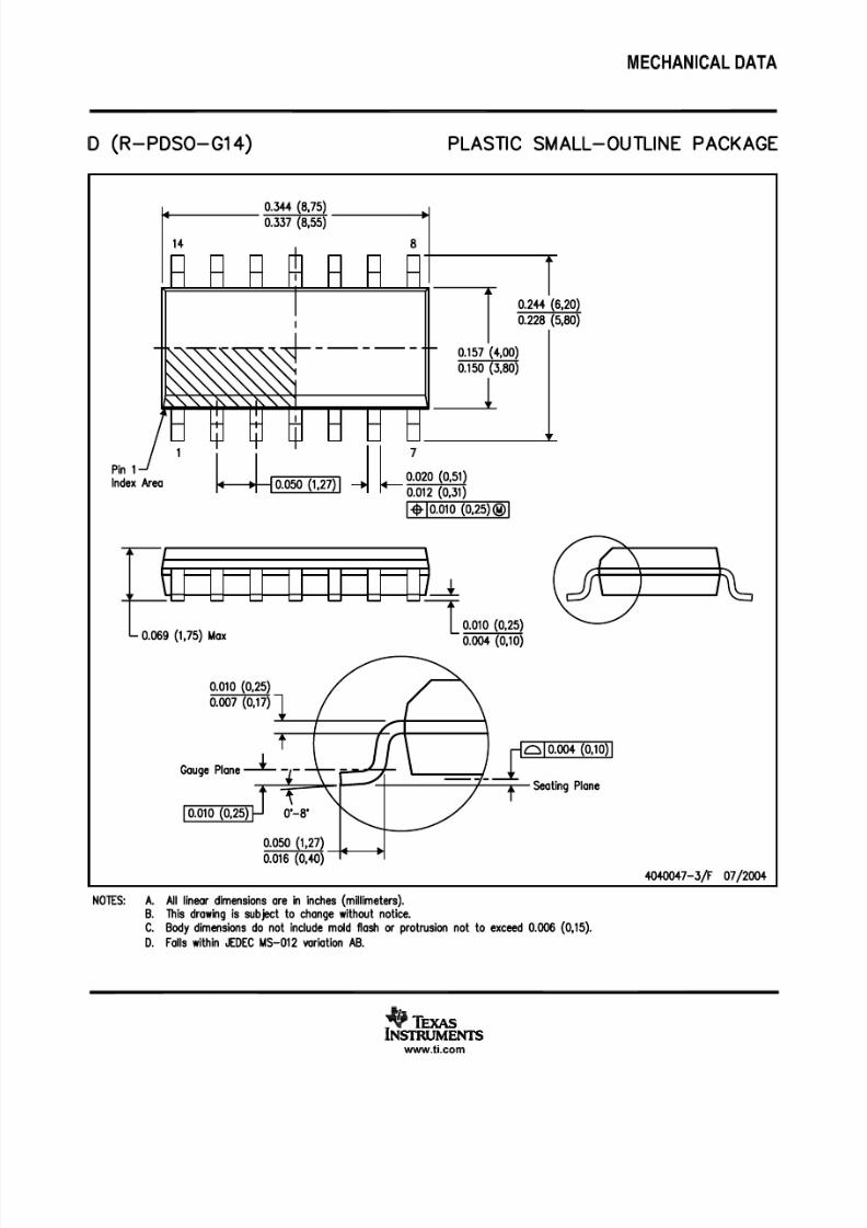
MTSS001C – JANUARY 1995 – REVISED FEBRUARY 1999
POST OFFICE BOX 655303 • DALLAS, TEXAS 75265
PW (R-PDSO-G**) PLASTIC SMALL-OUTLINE PACKAGE
14 PINS SHOWN
0,65 M0,10
0,10
0,25
0,50
0,75
0,15 NOM
Gage Plane
28
9,80
9,60
24
7,90
7,70
2016
6,60
6,40
4040064/F 01/97
0,30
6,60
6,20
8
0,19
4,30
4,50
7
0,15
14
A
1
1,20 MAX
14
5,10
4,90
8
3,10
2,90
A MAX
A MIN
DIM
PINS **
0,05
4,90
5,10
Seating Plane
0° –8°
NOTES: A. All linear dimensions are in millimeters.
B. This drawing is subject to change without notice.
C. Body dimensions do not include mold flash or protrusion not to exceed 0,15.
D. Falls within JEDEC MO-153

8/13/2019 DesktopTL 061CP2
http://slidepdf.com/reader/full/desktoptl-061cp2 35/36
IMPORTANT NOTICE
Texas Instruments Incorporated and its subsidiaries (TI) reserve the right to make corrections, modifications,
enhancements, improvements, and other changes to its products and services at any time and to discontinue
any product or service without notice. Customers should obtain the latest relevant information before placing
orders and should verify that such information is current and complete. All products are sold subject to TI’s terms
and conditions of sale supplied at the time of order acknowledgment.
TI warrants performance of its hardware products to the specifications applicable at the time of sale in
accordance with TI’s standard warranty. Testing and other quality control techniques are used to the extent TI
deems necessary to support this warranty. Except where mandated by government requirements, testing of all
parameters of each product is not necessarily performed.
TI assumes no liability for applications assistance or customer product design. Customers are responsible for
their products and applications using TI components. To minimize the risks associated with customer products
and applications, customers should provide adequate design and operating safeguards.
TI does not warrant or represent that any license, either express or implied, is granted under any TI patent right,
copyright, mask work right, or other TI intellectual property right relating to any combination, machine, or process
in which TI products or services are used. Information published by TI regarding third-party products or services
does not constitute a license from TI to use such products or services or a warranty or endorsement thereof.Use of such information may require a license from a third party under the patents or other intellectual property
of the third party, or a license from TI under the patents or other intellectual property of TI.
Reproduction of information in TI data books or data sheets is permissible only if reproduction is without
alteration and is accompanied by all associated warranties, conditions, limitations, and notices. Reproduction
of this information with alteration is an unfair and deceptive business practice. TI is not responsible or liable for
such altered documentation.
Resale of TI products or services with statements different from or beyond the parameters stated by TI for that
product or service voids all express and any implied warranties for the associated TI product or service and
is an unfair and deceptive business practice. TI is not responsible or liable for any such statements.
Following are URLs where you can obtain information on other Texas Instruments products and application
solutions:
Products Applications
Amplifiers amplifier.ti.com Audio www.ti.com/audio
Data Converters dataconverter.ti.com Automotive www.ti.com/automotive
DSP dsp.ti.com Broadband www.ti.com/broadband
Interface interface.ti.com Digital Control www.ti.com/digitalcontrol
Logic logic.ti.com Military www.ti.com/military
Power Mgmt power.ti.com Optical Networking www.ti.com/opticalnetwork
Microcontrollers microcontroller.ti.com Security www.ti.com/security
Telephony www.ti.com/telephony
Video & Imaging www.ti.com/video
Wireless www.ti.com/wireless
Mailing Address: Texas Instruments
Post Office Box 655303 Dallas, Texas 75265
Copyright © 2005, Texas Instruments Incorporated

8/13/2019 DesktopTL 061CP2
http://slidepdf.com/reader/full/desktoptl-061cp2 36/36
This datasheet has been download from:
www.datasheetcatalog.com
Datasheets for electronics components.


