Embed Size (px)
Citation preview

國 立 交 通 大 學
電機學院 電子與光電學程
碩 士 論 文
擴散電阻的靜電放電特性分析與防護設計上的應用
ESD Characteristics of Diffusion Resistor and its Application in On-chip ESD
Protection
研 究 生馮耀武
指導教授柯明道 教授
中 華 民 國 九 十 八 年 一 月
擴散電阻的靜電放電特性分析與防護設計上的應用
ESD Characteristics of Diffusion Resistor and its Application in On-chip ESD Protection
研 究 生馮耀武 StudentYao-Wu Feng
指導教授柯明道 AdvisorMing-Dou Ker
國 立 交 通 大 學
電機學院 電子與光電學程
碩 士 論 文
A Thesis
Submitted to Degree of Electrical and Computer Engineering
National Chiao Tung University
in partial Fulfillment of the Requirements
for the Degree of
Master of Science
in
Electronics and Electro-Optical Engineering
January 2009
Hsinchu Taiwan Republic of China
中華民國九十八年一月
i
擴散電阻的靜電放電特性分析與防護設計上的
應用
學生 馮 耀 武 指導教授 柯 明 道 教授
國立交通大學
電機學院 電子與光電學程碩士班
摘要
本論文是針對 silicided N+ 擴散電阻和 non-silicided N+ 擴散電阻在 100 奈
秒脈衝高電流加壓的條件下作出它的特性化和模型經由實際量測這兩種電阻
的阻值會隨著脈衝時間的方均根變化在電阻上的電流會隨加壓時間增加而減
少電阻上的電壓會隨加壓時間增加而增加電阻在高電流下造成非線性的電
壓-電流特性的原因可以用焦耳熱〈Joule-heating〉引起的電阻阻值改變來說明
另外本實驗所調查的這兩種電阻在高電流的條件下有不同的特性因為這種不
同的特性當這兩種電阻被應用在積體電路的靜電放電〈ESD〉防護上時其所
實現的佈局設計要有所不同
ii
ESD Characteristics of Diffusion Resistor and
its Application in On-chip ESD Protection
Design
Student Yao-Wu Feng Advisor Prof Ming-Dou Ker
Degree Program of Electrical and Computer Engineering
National Chiao-Tung University
ABSTRACT
The high current conduction in silicided N+ diffusion resistor and non-silicided
N+ diffusion resistor under the 100nsec pulse condition had been characterized and
modeled carefully in this work We find the resistances of both types resistors change
with the square root of the stress time It induces the current decreasing and voltage
increasing with the stress time The root cause of the non-linear IV characteristics of
the diffusion resistor under high current stress can be well explained by the
Joule-heating induced the resistance change In additional we also find that these two
diffusion resistors during high current stress will appear some different characteristics
Due to these different characteristics the silicided device cannot use the same layout
as the silicided blocking device on ESD protection design
iii
誌謝
首先我要感謝我的指導教授柯明道博士在這六年半來所給予我的指導與鼓
勵雖然在這段期間歷經工作上的壓力和家庭變故使得在課業上斷斷續續但
教授仍沒放棄指導甚至經由教授的幫忙讓我能夠兼顧工作與課業教授要求
我追求研究的完整性與嚴謹性使我體會到何謂研究教授指導我做研究的方
向方法與態度讓我對工作上的看法有了正面的改變而這種改變也讓我在
工作上提升經驗值教授的苦口婆心到最後才真正的有所體悟並且為此由衷
地感謝
在這裡也要特別感謝台積電李建興經理本篇論文是由李經理提供了 sample
讓我可以深入研究 diffusion resistor 的 ESD 特性及應用也指導了我很多研究
diffusion resistor 相關的方向另外雖然跟他共事的時間只有短短的一年但是
從他身上學到了很多東西尤其半導體製程對 ESD 保護電路的影響使我能將
所學與實務結合李經理在 ESD 領域的豐富經驗讓我縮短了對高壓製程 ESD
防護設計的學習曲線不論在工作上或課業上我從李經理身上獲益良多
另外我也要謝謝曾經在台積電的同事陳遂泓學長楊道宏先生和 TRP 實
驗室的同仁吳偉豪李仁豪蔡柏豪他們熱心教導我一些儀器的使用使我能
在量測上順利取得實驗數據並感謝吳國銘先生在製程上的協助
感謝林昆賢博士對於高壓製程給予專業的解答林群祐在論文撰寫格式上的
大力相助另外也謝謝 307 研究室的所有同學和學長姐們
我也感謝茂矽公司倪誠聰經理也是他的鼓勵與支持才讓我有繼續進修的動
力最後我要感謝我的家人尤其是我的太太李春櫻從未對我失去過信心這
一直是我精神上最大的支柱
還要感謝很多人不可勝數在此一併謝過我會持續努力進步來達成大家
的期盼
馮耀武
九十八年一月
iv
CONTENTS
ABSTRACT (CHINESE) helliphelliphelliphelliphelliphelliphelliphelliphelliphelliphelliphelliphelliphelliphelliphelliphelliphellip i
ABSTRACT (ENGLISH) helliphelliphelliphelliphelliphelliphelliphelliphelliphelliphelliphelliphelliphelliphelliphelliphelliphelliphelliphelliphelliphellip ii
ACKNOWLEDGEMENThelliphelliphelliphelliphelliphelliphelliphelliphelliphelliphelliphelliphelliphelliphelliphelliphelliphelliphelliphelliphelliphellip iii
CONTENTShelliphelliphelliphelliphelliphelliphelliphelliphelliphelliphelliphelliphelliphelliphelliphelliphelliphelliphelliphelliphelliphelliphelliphelliphelliphelliphellip iv
TABLE CAPTIONShelliphelliphelliphelliphelliphelliphelliphelliphelliphelliphelliphelliphelliphelliphelliphelliphelliphelliphelliphelliphelliphelliphelliphellip vi
FIGURE CAPTIONShelliphelliphelliphelliphelliphelliphelliphelliphelliphelliphelliphelliphelliphelliphelliphelliphelliphelliphelliphelliphelliphelliphellip vii
Chapter 1 Introductionhelliphelliphelliphelliphelliphelliphelliphelliphelliphelliphelliphelliphelliphelliphelliphelliphelliphelliphelliphelliphellip 1
Chapter 2 Experimenthelliphelliphelliphelliphelliphelliphelliphelliphelliphelliphelliphelliphelliphelliphelliphelliphelliphelliphelliphellip 3
Chapter 3 Results And Discussionshelliphelliphelliphelliphelliphelliphelliphelliphelliphelliphelliphelliphellip 9
31 DC IV CHARACTERISTIChelliphelliphelliphelliphelliphelliphelliphelliphelliphelliphelliphelliphelliphelliphelliphelliphelliphellip 9
32 HIGH CURRENT IV CHARACTERISTIC FOR RPO N+ DIFFUSION RESISTOR 10
33 REAL-TIME IV CHARACTERISTIC FOR RPO N+ DIFFUSION RESISTORhelliphellip 11
331 Linear Regionhelliphelliphelliphelliphelliphelliphelliphelliphelliphelliphelliphelliphelliphelliphelliphelliphelliphelliphelliphelliphelliphelliphellip 11
332 Thermal Regionhelliphelliphelliphelliphelliphelliphelliphelliphelliphelliphelliphelliphelliphelliphelliphelliphelliphelliphelliphelliphelliphellip 13
333 Saturation Regionhelliphelliphelliphelliphelliphelliphelliphelliphelliphelliphelliphelliphelliphelliphelliphelliphelliphelliphelliphelliphellip 15
334 Snapback Regionhelliphelliphelliphelliphelliphelliphelliphelliphelliphelliphelliphelliphelliphelliphelliphelliphelliphelliphelliphelliphelliphellip 16
34 HIGH CURRENT IV CHARACTERISTIC FOR SILICIDED N+ DIFFUSION
RESISTORhelliphelliphelliphelliphelliphelliphelliphelliphelliphelliphelliphelliphelliphelliphelliphelliphelliphelliphelliphelliphelliphelliphelliphelliphelliphelliphellip
18
35 REAL-TIME IV CHARACTERISTIC FOR SILICIDED N+ DIFFUSION RESISTOR 19
351 Linear Regionhelliphelliphelliphelliphelliphelliphelliphelliphelliphelliphelliphelliphelliphelliphelliphelliphelliphelliphelliphelliphelliphelliphellip 20
352 Thermal Regionhelliphelliphelliphelliphelliphelliphelliphelliphelliphelliphelliphelliphelliphelliphelliphelliphelliphelliphelliphelliphelliphelliphellip 21
353 Saturation Regionhelliphelliphelliphelliphelliphelliphelliphelliphelliphelliphelliphelliphelliphelliphelliphelliphelliphelliphelliphelliphelliphellip 22
36 ESD COMPARISON FOR SILICIDED AND RPO GROUNDED-GATE NMOShellip 23
Chapter 4 Applications For On-chip ESD Protection Designhelliphelliphelliphelliphellip 43
41 INPUT PIN ESD PROTECTION IMPROVEMENThelliphelliphelliphelliphelliphelliphelliphelliphelliphelliphelliphellip 43
42 OUTPUT PIN ESD PROTECTION IMPROVEMENThelliphelliphelliphelliphelliphelliphelliphelliphelliphelliphellip 44
Chapter 5 Conclusionshelliphelliphelliphelliphelliphelliphelliphelliphelliphelliphelliphelliphelliphelliphelliphelliphelliphelliphelliphellip 51
REFERENCEShelliphelliphelliphelliphelliphelliphelliphelliphelliphelliphelliphelliphelliphelliphelliphelliphelliphelliphelliphelliphelliphelliphelliphelliphelliphellip 52
v
VITAhelliphelliphelliphelliphelliphelliphelliphelliphelliphelliphelliphelliphelliphelliphelliphelliphelliphelliphelliphelliphelliphelliphelliphelliphelliphelliphelliphellip 53
vi
TABLE CAPTIONS
Table 31 Key layout parameter and ESD test resulthelliphelliphelliphelliphelliphelliphelliphelliphelliphelliphellip 26
Table 41 LVCESD structure splits ESD test resulthelliphelliphelliphelliphelliphelliphelliphelliphelliphelliphellip 46
Table 42 LVCESD structure with chip splits ESD test resulthelliphelliphelliphelliphelliphelliphellip 46
vii
FIGURE CAPTIONS
Fig 21 (a) Layout for RPO N+ diffusion resistor (b) Cross-section for RPO
N+ diffusion resistorhelliphelliphelliphelliphelliphelliphelliphelliphelliphelliphelliphelliphelliphelliphelliphellip
5
Fig 22 (a) Layout for Silicided N+ diffusion resistor (b) Cross-section for
Silicided N+ diffusion resistorhelliphelliphelliphelliphelliphelliphelliphelliphelliphelliphelliphelliphelliphellip
6
Fig 23 Apparatus for high current measurementhelliphelliphelliphelliphelliphelliphelliphelliphelliphellip 7
Fig 24 Layout for (a) Silicided NMOS (WL=720um04um) (b) RPO
NMOS (WL=300um04um)helliphelliphelliphelliphelliphelliphelliphelliphelliphelliphelliphelliphelliphellip
8
Fig 31 (a) DC IV Characteristics of a RPO N+ diffusion resistor vs
temperature (b) Resistance vs temperaturehelliphelliphelliphelliphelliphelliphelliphelliphellip
27
Fig 32 (a) DC IV Characteristics of a Silicided N+ diffusion resistor vs
temperature (b) Resistance vs temperaturehelliphelliphelliphelliphelliphelliphelliphelliphelliphellip
28
Fig 33 (a) Silicided N+ diffusion resistor has two conductor layers
(silicided film and N+ diffusion) (b) RPO N+ diffusion resistor only
has one conductor layer (N+ diffusion)helliphelliphelliphelliphelliphelliphelliphelliphelliphelliphellip
29
Fig 34 High current IV Characteristics of a RPO N+ diffusion resistor (a)
from linear region to snapback region (b) from linear region to
saturation regionhelliphelliphelliphelliphelliphelliphelliphelliphelliphelliphelliphelliphelliphelliphelliphelliphelliphelliphelliphellip
30
Fig 35 DC IV Characteristics of a RPO N+ diffusion resistorhelliphelliphelliphelliphellip 31
Fig 36 Linear region (a) Voltage and Current waveforms (b) Resistance
(VI) and power (VtimesI) vs time for a RPO N+ diffusion resistor
under the 100nsec TLP pulse eventhelliphelliphelliphelliphelliphelliphelliphelliphelliphelliphelliphellip
32
Fig 37 Thermal region (a) Voltage and Current waveforms (b) Resistance
(VI) and power (VtimesI) vs time for a RPO N+ diffusion resistor
under the 100nsec TLP pulse eventhelliphelliphelliphelliphelliphelliphelliphelliphelliphelliphelliphelliphellip
33
Fig 38 Equivalent circuit of a RPO N+ diffusion resistor under the 100nsec
TLP pulse eventhelliphelliphelliphelliphelliphelliphelliphelliphelliphelliphelliphelliphelliphellip
34
Fig 39 Saturation region (a) Voltage and Current waveforms (b)
Resistance (VI) and power (VtimesI) vs time for a RPO N+ diffusion
resistor under the 100nsec TLP pulse eventhelliphelliphelliphelliphelliphelliphelliphelliphelliphellip
35
Fig 310 Snapback region (a) Voltage and Current waveforms (b) Resistance
(VI) and power (VtimesI) vs time for a RPO N+ diffusion resistor
under the 100nsec TLP pulse eventhelliphelliphelliphelliphelliphelliphelliphelliphelliphelliphelliphelliphellip
36
Fig 311 The current (a) before the snapback region (b) at the snapback
regionhelliphelliphelliphelliphelliphelliphelliphelliphelliphelliphelliphelliphelliphelliphelliphelliphelliphelliphelliphelliphelliphelliphelliphelliphellip
37
Fig 312 The measured substrate potential (B in Fig 311) for the stress in
viii
Fig 310helliphelliphelliphelliphelliphelliphelliphelliphelliphelliphelliphelliphelliphelliphelliphelliphelliphelliphelliphelliphelliphelliphellip 37
Fig 313 (a) High current IV Characteristics of a Silicided N+ diffusion
resistor (b) Zoom-Inhelliphelliphelliphelliphelliphelliphelliphelliphelliphelliphelliphelliphelliphelliphelliphelliphelliphellip
38
Fig 314 Linear region (a) Voltage and Current waveforms (b) Resistance
(VI) and power (VtimesI) vs time for a silicided N+ diffusion resistor
under the 100ns pulse eventhelliphelliphelliphelliphelliphelliphelliphelliphelliphelliphelliphelliphelliphelliphelliphellip
39
Fig 315 Thermal region (a) Voltage and Current waveforms (b) Resistance
(VI) and power (VtimesI) vs time for a silicided N+ diffusion resistor
under the 100nsec TLP pulse eventhelliphelliphelliphelliphelliphelliphelliphelliphelliphelliphelliphelliphellip
40
Fig 316 Saturation region (a) Voltage and Current waveforms (b)
Resistance (VI) and power (VtimesI) vs time for a silicided N+
diffusion resistor under the 100nsec TLP pulse eventhelliphelliphelliphelliphellip
41
Fig 317 High current IV characteristics of (a) silicided NMOS
(WL=720um04um) (b) RPO NMOS (WL=300um04um)hellip
42
Fig 41 Low trigger Voltage and low Capacitance ESD protection device
(LVCESD) (a) top view (b) cross-sectionhelliphelliphelliphelliphelliphelliphelliphelliphelliphellip
47
Fig 42 LVCESD splits (a) split structure (b) TLP curve comparisonhelliphelliphellip 48
Fig 43 LVCESD splits structure (a) LVCESD (b) LVCESD with 10Ω N+
poly resistor (c) LVCESD with 2nd
ESD (Silicided NMOS
WL=20um025um) (d) LVCESD with 2nd
ESD (Silicided NMOS
WL=20um025um) and 10Ω N+ poly resistorhelliphelliphelliphelliphelliphelliphelliphellip
49
Fig 44 IV characteristics of a n+ diffusion resistor (WL=5um60um) (a)
Cathode and substrate(1) current vs anode-to-cathode voltage with
the reverse-bias characteristics of the same well-substrate diode(2)
added for reference (b) The related static (Rs) and dynamic (Rd)
resistance vs anode-to-cathode voltagehelliphelliphelliphelliphelliphelliphelliphelliphelliphelliphellip
49
Fig 45 IV characteristics of a n-well diffusion resistor (WL=70um14um)
(a) Cathode and substrate current vs anode-to-cathode voltage (b)
The related static (Rs) and dynamic (Rd) resistance vs
anode-to-cathode voltagehelliphelliphelliphelliphelliphelliphelliphellip
50
Fig 46 Output buffer with a ldquodecouple resistorrdquo (a) Main discharge through
a protection device N1 (b) Main discharge via the p-source to Vcc
diode and the equivalent discharge path between the Vcc and Vss
lineshelliphelliphelliphelliphelliphelliphelliphelliphelliphelliphelliphelliphelliphelliphelliphelliphelliphelliphelliphelliphelliphelliphelliphelliphellip
50
1
Chapter 1
Introduction
The passive component (diffusion resistor) had been commonly used by the
integrated circuit industry for a variety of applications Most of these applications is
related to low power operation and as such is not concerned the high current-level
and the resulting effects However the diffusion resistor can be the component of the
electrostatics discharge (ESD) protection circuit or is connected in series with output
buffer to suppress the transition noise which are subjected to high current density
level and the resulting effects
The purpose of this work is to characterize and model the high current effects in
the two common used diffusion resistors under a 100nsec transmission line pulse
(TLP) condition and evaluate the electrical and thermal stability of the two diffusion
resistors Currently there is limited information available on the high current and
self-heating effects on these structures [1]-[2] And it can find an obvious error on the
theoretical model for the diffusion resistor under the high current TLP stress event [2]
Although they had observed abnormal IV during the stress period they still assume
the stress current is a constant and does not vary with time during the stress period
[2]
This paper will present a model based on Wunsch-Bell model [3] and identify
important parameters related to the high current effects on the silicided diffusion
resistor and silicided blocking (RPO) diffusion resistor An understanding of these
high current effects will enable the impact of technology scaling of silicided film to be
defined for the development of future nanometer technology and how to develop the
2
robust ESD protection device
Chapter 2 describes two types of diffusion resistorsrsquo structure and NMOS
Apparatus for high current measurement is also shown in this chapter Chapter 3
shows the experimental results and discussion There is a model built in this chapter
And make a comparison between silicided NMOS and non-silicided NMOS Chapter
4 describes the resistor application on ESD protection Chapter 5 is the conclusions of
this thesis
3
Chapter 2
Experiment
The technology used in this work is the 025-um CMOS silicided process The
silicided for this technology is Ti silicide (TiSi2) This technology also includes one
silicided blocking (RPO) process to prevent the silicided film formation on the
diffusion or poly if one wants to build the high resistance resistors in the chip for ESD
purpose or circuit application As a region is covered by the silicided blocking layer
(RPO) this region will become a non-silicided region The used resistors for this
study are RPO N+ diffusion resistor (Fig 21) and silicided N+ diffusion resistor (Fig
22) The resistor has three terminals The first terminal is used to apply the stress
voltage (region A in Fig 21 and Fig 22) The second terminal is used to monitor the
substrate potential of the diffusion resistor under the TLP stress event (region B in Fig
21 and Fig 22) The third terminal is the grounded terminal which includes a P+
diffusion and a N+ diffusion (region C in Fig 21 and Fig 22)
Fig 23 shows the apparatus used for the high current IV characteristics
measurement of the resistor under the TLP pulse The TLP system is used for this
measurement is the commercial Barth-TLP system It can generate the 02nsec rising
time and 100nsec pulse width single pulse and continuously increase the stress current
up to 10A The pulse is applied to one terminal of the resistor (region A) with
respective to the grounded substrate and other terminal (region C) A 500MHz digital
oscilloscope with 4Gsec sampling rate is used to capture the voltage substrate
potential and current waveforms simultaneously The voltages are measured using
voltage probes and the current is measured using a 1mA to 5mV current probe (Tek
4
CT-1)
For silicided gate-ground NMOS and non-silicided (RPO) gate-ground NMOS
the layouts are shown in Fig 24 The ESD performance comparison of these two
devices is also presented in this report
5
P+ diffusion
N+
diffu
sio
n
Silicide-blocking
layer
M1(C)
M1 (A)
M1 (B)
floating
P+ pick-up
P+ diffusion
N+
diffu
sio
n
Silicide-blocking
layer
M1(C)
M1 (A)
M1 (B)
floating
P+ pick-up
L
W
P+ diffusion
N+
diffu
sio
n
Silicide-blocking
layer
M1(C)
M1 (A)
M1 (B)
floating
P+ pick-up
P+ diffusion
N+
diffu
sio
n
Silicide-blocking
layer
M1(C)
M1 (A)
M1 (B)
floating
P+ pick-up
L
W
(a)
(b)
Fig 21 (a) Layout for RPO N+ diffusion resistor (WL=2um3um) (b) Cross-section
for RPO N+ diffusion resistor
6
P+ guard-ring
N+
diffu
sio
n
M1(C)
M1 (A)
M1(B)
floating
P+
pick-up
P+ guard-ring
N+
diffu
sio
n
M1(C)
M1 (A)
M1(B)
floating
P+
pick-up
L
W
P+ guard-ring
N+
diffu
sio
n
M1(C)
M1 (A)
M1(B)
floating
P+
pick-up
P+ guard-ring
N+
diffu
sio
n
M1(C)
M1 (A)
M1(B)
floating
P+
pick-up
L
W
(a)
SilicideSilicide
(b)
Fig 22 (a) Layout for Silicided N+ diffusion resistor (WL=2um165um) (b)
Cross-section for Silicided N+ diffusion resistor
7
Fig 23 Apparatus for high current measurement
8
OD
Poly
RPO
Contact
OD
Poly
RPO
Contact
OD
Poly
RPO
Contact
(a)
(b)
Fig 24 Layout for (a) Silicided NMOS (WL=720um04um) (b) RPO NMOS
(WL=300um04um)
9
Chapter 3
Results and Discussions
31 DC IV Characteristic
Fig 31(a) and Fig 32(a) show the DC IV characteristics of the RPO N+
diffusion resistor and silicided N+ diffusion resistor versus the temperature (25degC
75degC and 125
degC) The applied voltage is from 0V to 01V to make sure without
Joule-heating generating during the measurement So the current can increase with
the applied voltage linearly and decrease with the temperature Fig 31(b) and 32(b)
show the resistances of the two kinds of the diffusion resistors versus the temperature
based on above the measured results The resistances for the two kinds of the
diffusion resistors increase with the temperature linearly and follow the well known
equation for the diffusion resistor
R(T)=Ro(1+β T) (1)
where R(T) is the dynamic resistance at temperature T(degC) β is the temperature
coefficient of the diffusion resistor Ro is the initial resistance at 0degC
Based on this equation and the results in Fig 31(b) and 32(b) the temperature
coefficients are 000115degC and 000360
degC for RPO N+ diffusion resistor and
silicided N+ diffusion resistor respectively Although the sheet resistance of the RPO
N+ diffusion resistor (115Ω) is much higher than that of the silicided N+ diffusion
resistor (37Ω) the temperature coefficient of the RPO N+ diffusion resistor is
smaller than that of the silicided N+ diffusion resistor It is because that the silicided
N+ diffusion resistor has two conduction layers (silicided film and N+ diffusion) but
the RPO N+ diffusion resistor only has one conduction layer (N+ diffusion) as shown
10
in Fig 33 And the more importance is that the silicided film is similar to a metal
layer So for silicided N+ diffusion resistor most stress current will be confined in the
small thickness silicided film resulting in high current density Compared with
silicided N+ diffusion resistor the current density of the RPO N+ diffusion resistor is
smaller since the thickness of the N+ junction is thicker than that of the silicided film
Although the silicided N+ diffusion resistor has much higher current capability ESD
designer still uses the RPO N+ diffusion resistor to make the device ESD performance
more robust
32 High Current IV Characteristic For RPO N+ Diffusion Resistor
Fig 34 shows the high current I-V characteristics of the RPO N+ diffusion
resistor under the 100nsec TLP stress event The set-up is shown in Fig 23 A
100nsec current pulse is applied to one node of the RPO N+ diffusion resistor (A in
Fig 23) with respect to the grounded node of the RPO N+ diffusion resistor and
P-substrate (C in Fig 23) The stress current level is increased continuously until the
RPO N+ diffusion resistor was damaged The voltage and current waveforms of the
RPO N+ diffusion resistor during the TLP stress period are measured simultaneously
by the oscillator-scope during the TLP stress period After each TLP stress a DC
meter is used to check the variation of the leakage current of the RPO N+ diffusion
resistor for judging whether the RPO N+ diffusion resistor was damaged by the TLP
stress or not All measured datarsquos are transferred to a computer by an IEEE-488 cable
The computer records the data at 20nsec prior to the end of the TLP pulse and leakage
current to the disk Based on the recorded values at each stress level the high current
IV characteristics of the device are constructed as shown in Fig 34
It is apparent that the high current IV characteristics of a RPO N+ diffusion
11
resistor can be divided by four regions (linear region thermal region saturation
region and snapback region) For linear region the current increases with the voltage
linearly Compared with linear region the current in the thermal region only can
slightly increase with the voltage As it goes into the saturation region the current
cannot increase with the voltage any more The current was clamped as a constant in
this region until the applied voltage higher than the diffusion avalanche breakdown
voltage Fig 35 shows the DC IV curve of the RPO N+ diffusion resistor The current
increases significantly if the applied voltage is higher than 85V As the applied
voltage is higher than the avalanche breakdown voltage an apparent snapback
phenomenon can be found in Fig 34 The current at this region is higher than the
saturation current But the voltage is smaller than the avalanche breakdown voltage
33 Real-Time IV Characteristic For RPO N+ Diffusion Resistor
Because the high current IV curve only recodes a single point IV of the RPO N+
diffusion resistor under a 100nsec TLP stress event it only can tell us that there are
four different characteristics from low stress current to high stress current for the RPO
N+ diffusion resistor but it cannot tell why it has the four different characteristics In
order to investigate the detail insight of a RPO N+ diffusion resistor under the TLP
stress event the voltage and current waveforms are used to analysis and see what is
going on for a RPO N+ diffusion resistor under the TLP stress event
331 Linear Region
Fig 36(a) shows the current and voltage waveforms of the RPO N+ diffusion
resistor in the linear region under a 100nsec TLP stress event From 30nsec to 52nsec
the pulse travels through the measured probes to the RPO N+ diffusion resistor and
12
bounces back to the measured probes (Fig 23) At this period the voltage and current
are the constants Because of the difference in impedances between the cable and the
test device the pulse will be reflected based on the formula Γ=(ZL-ZO)(ZL+ZO) [4] as
the pulse reaches the device The reflected wave will travel back to the TLP system
[5] As the reflected wave reaches the voltage probe and current probe one may
observe that voltage has increased sharply and current decreased sharply This is
because the pulse is a combination of a reflected wave and an incident wave To do
the TLP measurement it needs the probe or wire as the inter-connector to connect the
TLP system and the pad of the RPO N+ diffusion resistor The probe or the wire acts
as an inductor during the rising and falling stages of TLP stress pulse This gives rise
of the voltage (LdIdt) and decreases the current when the pulse touches the RPO N+
diffusion resistor since the inductor current cannot be changed in an instant After this
transient (~52nsec) the pulse starts to stress the device After 131nsec there is no
incident wave coming in from the TLP system and it has only a reflected wave
traveling back from the device to the measurement probes as one may observe from
the oscilloscope One may observe that the current has decreased below 0A since by
now only the reflected wave exists
Based on the measured voltage and current in Fig 36(a) the dynamic resistance
(V(t)I(t)) and the generated power (V(t)timesI(t)) can be obtained as shown in Fig 36(b)
It can be found that the resistance and the generated power can keep as the constants
at the TLP pulse stress period Because this stress level only generates several
milli-wattrsquos and the P-substrate can provide a good heating-sink source the
Joule-heating generated by the power can be transferred into the substrate completely
and without leaving any Joule-heating in the RPO N+ diffusion resistor during the
TLP pulse stress period So the temperature of the RPO N+ diffusion resistor can be
kept as a constant
13
Based on eq (1) the resistance will be a constant and the current can linearly
increase with the voltage if the stress condition does not lead the RPO N+ diffusion
resistor temperature increasing This is why the current of the RPO N+ diffusion
resistor can linearly increase with the voltage if it is biased at the linear region
332 Thermal Region
Fig 37(a) shows the thermal region current and voltage waveforms of the RPO
N+ diffusion resistor under a 100nsec TLP stress event It can be found that the
current decreases and the voltage increases continuously during the TLP stress period
Based on the measured voltage and current in Fig 37(a) the dynamic resistance
(V(t)I(t)) and the generated power (V(t)timesI(t)) can be obtained as shown in Fig 37(b)
It can be found that the resistance increases and the generated power decreases with
the TLP stress time Because the generated power caused by this stress had reached
several hundred milli-watt the P-substrate cannot sink all Joule-heating generated
from the power in an instant As the RPO N+ diffusion resistor biased at the thermal
region part of the Joule-heating can be transferred into the P-substrate and part of the
Joule-heating still left in the RPO N+ diffusion resistor to result in the increase in the
temperature of the RPO N+ diffusion resistor Fig 38 shows the equivalent circuit of
a RPO N+ diffusion resistor under the TLP stress event The output resistance Rs of
the TLP system is 50ohm Unlike the resistance of the tested RPO N+ diffusion
resistor varied with the TLP stress time the TLP output resistance Rs does not vary
with the stress current and can be treated as a constant resistance during the TLP
stress period And the output voltage Vs of the TLP system during the TLP stress
period can be treated as a constant voltage Based on the equivalent circuit the
resistance change will cause the voltage and current varied with the TLP stress time
))(()( tRRVtI ss (2)
14
))(()()( tRRtRVtV ss (3)
Based on Wunsch-Bell model [3] the increase in the temperature of a RPO N+
diffusion resistor under a square pulse is a function of the stress time and given by
tkPtT )( (4)
where generated power P can be approximated as a constant ( 2
00
2 )( RRRV SS )
during a square pulse
Substituted eq(4) into eq (1) the dynamic resistance can be expressed as
)1()( 0 taRtR (5)
where a=kβ P
So the current varied with the stress time can be expressed as
))1(()( 0 taRRVtI ss (6)
And the voltage varied with the stress time can be expressed as
))1(()1()( 00 taRRtaRVtV Ss (7)
From eq (4) we know that the Joule-heating caused by the generated power (P)
will induce the temperature of the RPO N+ diffusion resistor increasing And the
increase in the RPO N+ diffusion resistor temperature will cause the resistance
increasing based on eq (1) From eq (5) the resistance of a RPO N+ diffusion
resistor under a TLP stress increases with the square root of the stress time Fig 37
shows that the calculated resistance based on eq (5) can fit the measured resistance
Based on eq (6) and eq (7) the increase in the resistance will induce the voltage
increasing and current decreasing as the observed result in Fig 37(a) All the
calculated values based on eq (6) and eq (7) can fit the measured curves very well
Based on eq (1) and the result in Fig 37(b) this stress will lead in the temperature of
the RPO N+ diffusion resistor increasing about 470degC at the end of the pulse
15
333 Saturation Region
Fig 39(a) shows the current and voltage waveforms of the RPO N+ diffusion in
the saturation region resistor under a 100nsec TLP stress event Compared with the
thermal region current (45mA to 30mA) the decrease in the magnitude of the current
(50mA to 30mA) is more sharply It can be found that the generated power (035W)
for the thermal region is higher than that (027W) of the thermal region (Fig 39(b))
The higher the power is the higher the Joule-heating leaves in the RPO N+ diffusion
resistor to cause the higher increase in the temperature of the RPO N+ diffusion
resistor Based on eq (1) and the result in Fig 39(b) this stress will lead in the
temperature of the RPO N+ diffusion resistor increasing about 690degC at the end of the
pulse
Same behavior as the RPO N+ diffusion resistor in the thermal region the
resistance increases with the square root of the TLP stress time followed the eq (5) as
shown in Fig 39(b) As the resistance increases with the square root of the TLP stress
time it will induce the stress current decreasing and voltage increasing continuously
with the TLP stress time (Fig 39(a)) which follows the eq (6) and (7)
By comparing the Fig 37(a) and Fig 39(a) it can be found that the initial
current and voltage (~52nsec in Fig 37(a) and 39(a)) can increase with the applied
voltage Vs Subsequently the current decreases and voltage increases with the TLP
stress time continuously following the above equations Because the resistance
increase follows the square root term of the TLP stress time the resistance curve will
show a sharp rising slop at the beginning of the pulse (52nsec~80nsec) and become
flat at the end of the pulse (100nsec~132nsec) It is worth noting that the high current
IV (Fig 34(a)) only records the measured point prior to the end of the pulse 20nsec
From eq (6) the current is a function of the applied voltage Vs divided by the
summation of a constant resistance (Rs) and a dynamic resistance But the dynamic
16
resistance is a function of the applied voltage based on eqs (1) and (4) and can be
expressed as
))(1()( 2
00
2
0 RRtRkVRtR SS (8)
At the beginning of the stress pulse the second term is small and can be
neglected So the stress current still increases with the applied voltage As the stress
time is long enough the second term of eq (8) becomes important It can compensate
the increase in the current caused by the applied voltage resulting in the current
independent of the applied voltage So the stress voltage still can increase with stress
voltage but the stress current will be clamped to a constant for the longer time stress
This is why the high current IV (Fig 34) shows that the current cannot be increased
at the saturation region If the recording data point is at other region the high current
IV curve of the RPO N+ diffusion resistor will not appear the saturation characteristic
334 Snapback Region
Fig 310(a) shows the current and voltage waveforms of the RPO N+ diffusion
resistor in the snapback region under a 100nsec TLP stress event For this stress the
applied voltage (~9V) in the initial transient (50nsec~95nsec) is apparently higher
than the breakdown voltage of the N+ diffusion 85V based on the DC IV measured
result in Fig 35 Unlike the stress currents of the linear region thermal region and
saturation region the current of the snapback region cannot be confined in the RPO
N+ diffusion resistor any more Most of the current still flows through the RPO N+
diffusion resistor but part of the current flows into the P-substrate and through the
P-Well resistor (R-sub) to Vss (Fig 311(a)) This gives rise of the substrate potential
as shown in Fig 312 In this test structure a floating P+ pick-up (Fig 22) is
designed to monitor the P-substrate potential variation of the RPO N+ diffusion
17
resistor during the TLP stress period The set-up for substrate potential is shown in
Fig 23
Like the behavior of the thermal region and saturation region the RPO N+
diffusion resistor resistance increases with the stress time caused by the RPO N+
diffusion resistor temperature increasing due to power induced the Joule-heating
generation (Fig 312) The increase in the RPO N+ diffusion resistor resistance will
decrease the current flowing through the RPO N+ diffusion resistor to push more
current flowing into the P-substrate resulting in the substrate potential increasing
gradually as shown in Fig 312 (50nsec~95nsec) As the substrate potential reaches
the critical point (07V at the stress time 95nsec in Fig 312) the junction between the
P-substrate and the cathode of the RPO N+ diffusion resistor will be forwarded
resulting in the cathode of the RPO N+ diffusion resistor injecting the electrons
These injected electrons will be collected by the anode of the RPO N+ diffusion
resistor This action can be treated as the npn bipolar turned on (Fig 311(b)) As the
npn bipolar turned on it can provide a very low impedance conduction path to sink
much more than the current that the RPO N+ diffusion resistor can sink The resistor
during the snapback region can be treated as a RPO N+ diffusion resistor and on
resistor of an npn bipolar in parallel But the on resistor resistance of an npn bipolar
is much smaller than the RPO N+ diffusion resistor resistance We can find the
resistance during the snapback region is apparently is much smaller than that of the
region before occurred the snapback This induces the current increasing and voltage
decreasing drastically So an apparent snapback phenomenon can be found after the
transient 95nsec in Fig 311(a) Then a lot of current will flow though the P-substrate
to result in the substrate potential at region B in Fig 311 increases sharply
18
34 High Current IV Characteristic For Silicided N+ Diffusion
Resistor
Fig 313 shows the high current I-V characteristics of a silicided N+ diffusion
resistor under the 100nsec TLP stress event The set-up is shown in Fig 23 A
100nsec current pulse is applied to one node of the silicided N+ diffusion resistor (A
in Fig 23) with respective to the grounded node of the silicided N+ diffusion resistor
and P-substrate (C in Fig 23) The stress current level is increased continuously until
the silicided N+ diffusion resistor was damaged The voltage and current waveforms
of the silicided N+ diffusion resistor during the TLP stress period are measured
simultaneously by the oscillator-scope After each TLP stress a DC meter is used to
check the variation of the leakage current of the silicided N+ diffusion resistor for
judging whether the silicided N+ diffusion resistor was damaged by the TLP stress or
not All measured datarsquos are transferred to a computer by an IEEE-488 cable The
computer records the data at 20nsec prior to the end of the TLP pulse and leakage
current to the disk Based on the recorded values at each stress level the high current
IV characteristics of the device are constructed as shown in Fig 313
Although the high current IV characteristics of the silicided N+ diffusion resistor
also can be divided by four regions it does not be found the snapback phenomenon
even at high current stress level The four regions for silicided N+ diffusion resistor
are linear region thermal region saturation region and breakdown region For linear
region the current increases with the voltage linearly Compared with the linear
region the rising slop of the current at the thermal region is more gradient As it goes
into the saturation region the current cannot increase with the voltage any more It is
worth noting that the saturation current for silicided N+ diffusion resistor (135mA) is
larger than that of the RPO N+ diffusion resistor (33mA) since the silicided N+
diffusion resistor includes two conduction layers (silicided film and N+ diffusion) and
19
the current conduction capability of silicided film is higher than that of RPO N+
diffusion
Unlike the RPO N+ diffusion resistor that can be driven into the snapback when
the applied voltage higher than the junction avalanche breakdown voltage the current
for the silicided N+ diffusion resistor still can be kept as a constant even the applied
voltage higher than the junction avalanche breakdown voltage (85V as shown in Fig
35) This difference is caused by that the two test structures have different P+
diffusion layouts For RPO N+ diffusion resistor the P+ diffusion used as the ground
is below the cathode of the RPO N+ diffusion resistor (Fig 22) For silicided N+
diffusion resistor the P+ diffusion used as the ground is a guard-ring which surrounds
the silicided N+ diffusion resistor completely This kind layout will decrease the
resistance of the substrate resistor (Rsub in Fig 311(a)) significantly to result in the
turn-on condition for a bipolar (IsubtimesRsub) hard to achieve So the snapback
phenomenon cannot be found and the silicided N+ diffusion resistor only can be
biased at avalanche region if the applied voltage is higher than the junction
breakdown voltage
35 Real-Time IV Characteristic For Silicided N+ Diffusion Resistor
Same reason as we talked in the RPO N+ diffusion resistor a single recoding
point IV can not tell us whatrsquos going on of the silicided N+ diffusion resistor during
the TLP stress event So the whole voltage and current waveform are used to
investigate the detail insight of a silicided N+ diffusion resistor under the TLP stress
event
20
351 Linear Region
Fig 314(a) shows the current and voltage waveforms of the silicided N+
diffusion resistor in the linear region under a 100nsec TLP stress event From 25nsec
to 52nsec the pulse travels through the measured probes to the silicided N+ diffusion
resistor and bounces back to the measured probes (Fig 23) At this period the
voltage and current are the constants Compared the Fig 36(a) and Fig 314(a) the
voltage waveform of the silicided N+ diffusion resistor during the TLP stress period is
apparently different from that of the RPO N+ diffusion resistor during the TLP stress
period It is because of that the resistance of the silicided N+ diffusion resistor (~30Ω)
is smaller than the TLP output resistance (50Ω) but the resistance of the RPO N+
diffusion resistor (~170Ω) is much larger than the TLP output resistance (50Ω)
Except the resistor resistance the inductance caused by the bonding wire or probe is
needed to count into the impedance for the loading (ZL) But it is well known that the
impedance caused by the inductance is arisen from LdIdt So it only can affect the
voltage waveform at the beginning of the TLP stress due to large dIdt (B in Fig
314(a)) but can be neglected after this transient due to nearly zero dIdt
Adding the inductance will cause the loading impedance ZL larger than the TLP
output resistance to generate a positive reflected wave based on the formula
Γ=(ZL-Z0)(ZL+Z0) resulting in the voltage higher than the initial voltage (Vi in Fig
314(a)) Without the inductance the impedance of the silicided N+ diffusion resistor
becomes smaller than the TLP output resistance to induce a negative reflected
waveform resulting in the voltage smaller than the initial voltage (Vi in Fig 314(a))
Based on the measured voltage and current in Fig 314(a) the dynamic
resistance (V(t)I(t)) and the generated power (V(t)timesI(t)) can be obtained as shown in
Fig 314(b) It can be found that the resistance and the generated power all can keep
as the constants during the TLP stress period since the Joule-heating generated by the
21
power is still quite low and all can be transferred into the substrate completely
Without the additional heat the silicided N+ diffusion resistor temperature does not
vary with the TLP stress time and the resistance can keep as the constant based on eq
(1) So the current of the silicided N+ diffusion resistor can linearly increase with the
voltage as it is biased at the linear region
352 Thermal Region
Fig 315(a) shows the current and voltage waveforms of the silicided N+
diffusion resistor in the thermal region under a 100nsec TLP stress event It can be
found that the current decreases and the voltage increases continuously during the
TLP stress period Based on the measured voltage and current in Fig 315(a) the
dynamic resistance (V(t)I(t)) and the generated power (V(t)timesI(t)) can be obtained as
shown in Fig 315(b) It can be found that the resistance increases with the TLP stress
time and the generated power is nearly a constant during the TLP stress period Same
mechanism as the discussion in the thermal region for RPO N+ diffusion resistor the
P-substrate can not sink all Joule-heating generated from the power in an instant to
leave part of Joule-heating in the silicided N+ diffusion resistor resulting in the
increase in the temperature of the silicided N+ diffusion resistor The detail
mechanism that the current and voltage varied with the TLP stress time had been
discussion in the section of the thermal region for RPO N+ diffusion resistor Based
on eq(1) and the result in Fig 315(b) this stress will lead in the temperature of the
silicided N+ diffusion resistor increasing about 139degC Compared with the RPO N+
diffusion resistor the temperature increase at the thermal region for the silicided N+
diffusion resistor is nearly 13 of the temperature increase for the RPO N+ diffusion
resistor since the temperature coefficient of the silicided N+ diffusion resistor is
nearly three times of the RPO N+ diffusion resistor
22
353 Saturation Region
Fig 316(a) shows the saturation region current and voltage waveforms of the
silicided N+ diffusion resistor under a 100nsec TLP stress event Compared with the
current in the thermal region (108mA to 99mA) the saturation current decreases more
sharply (148mA to 113mA) The generated power (~1W) during the saturation region
(Fig 316(b)) is nearly twice of the generated power (05W) during the thermal region
(Fig 315(b)) The more power is generated the more Joule-heating leaves in the
silicided N+ diffusion resistor to induce in the higher temperature for the silicided N+
diffusion resistor Based on eq (1) and the result in Fig 316(b) this stress will lead
the temperature of the silicided N+ diffusion resistor increasing about 224degC at the
end of the pulse which is much higher than the increase in the temperature of the
silicided N+ diffusion resistor during the thermal region (139degC) but much smaller
than the increase in the temperature of the RPO N+ diffusion resistor during the
saturation region (690degC) Fig 316(b) shows that the silicided N+ diffusion resistor
also can follow eq (6) which resistance increases with the square root of the stress
time Thus the current and voltage also can follow the eqs (7) and (8) to increase and
decrease with the stress time respectively By comparing Figs 37(b) and 15(b) or
Figs 39(b) and 16(b) it can be found that the generated power for silicided N+
diffusion resistor during the TLP stress period is nearly a constant that does not vary
with the stress time while the generated power for the RPO N+ diffusion resistor
during the TLP stress period decreases with the stress time It implies that the thermal
conduction for RPO N+ diffusion resistor is better than the silicided N+ diffusion
resistor The more heat transferred into the P-substrate the less power left in the RPO
N+ diffusion resistor So the generated power will decrease with the stress time The
less heat transferred into the P-substrate the more power left in the silicided N+
diffusion resistor So the generated power does not vary with the stress time This
23
difference might be caused by that the current of the silicided N+ diffusion resistor is
confined in the thin silicided film to induce the local heating but the current of RPO
N+ diffusion resistor can flow whole junction and the junction is just above the large
heat-sink P-substrate Because the Joule-heating induced the device temperature
increasing higher than the silicon melting point is the main cause of the ESD failure
the device will have poor ESD performance if it has the bad thermal conductivity
This is why we often think that the silicided process will degrade the device ESD
performance
36 ESD Comparison For Silicided And RPO Grounded-Gate NMOS
The self-protection scheme which NPMOS drivers are the ESD protection
devices is commonly used for digital IO ESD protection Using this scheme the
NMOS will dominate the ESD event So NMOS is much more important than the
PMOS for IO ESD protection in CMOS technology Up to now ESD designers often
have the concept that the silicided process will degrade the device ESD performance
So various schemes from process (silicided block (RPO) [6]) and circuits (gate
coupling [7] and substrate trigger [8]) are proposed to improve the NMOS ESD
performance But the RPO scheme seems more popular than other schemes since
most foundries provide the RPO design rules for customers as the reference And
most ESD designers accept the concept that RPO can build a ballast resistor [9] for
NMOS But most people do not know why NMOS needs a ballast resistor drain In
fact the ESD event can be treated as a constant current stress event Whether the
device has a ballast resistor cannot change the ESD stress current level [10] and the
current capability of the silicided N+ diffusion resistor is apparently much higher than
that of the RPO N+ diffusion resistor from above experiment result If the silicided
24
N+ diffusion resistor can sustain more current than the RPO N+ diffusion resistor it
does not have the reason that the silicided device is more vulnerable to ESD stress
than the RPO device So the ballast resistor concept cannot explain why using RPO
to forbid the silicided formation on the drain can improve the device ESD
performance In fact we find the silicided device can be designed as robust as or even
better than the RPO device
As we discussed in the above sections we can conclude some different
characteristics for RPO N+ diffusion resistor and silicided N+ diffusion resistor 1
the thermal conductivity of the RPO N+ diffusion resistor is better than the silicided
N+ diffusion resistor 2 the saturation current of the silicided N+ diffusion resistor is
higher than that of RPO N+ diffusion resistor 3 for silicided N+ diffusion resistor
most current will be confined in the silicided film 4 for RPO N+ diffusion resistor
the current can distribute whole junction Because of these different behaviors the
silicided grounded-gate NMOS (GGNMOS) and RPO GGNMOS cannot use same
kind layout if one wants to get good ESD performance for these two devices
Fig 24 shows the layouts of these two devices Table 31 lists the key
parameters and ESD test results for these two devices The dimensions for these two
devices are almost the same (silicided GGNMOS 30times336=1008um2 RPO GGNMOS
30times3395=10185um2) Based on characteristic 4 the current of the RPO N+ diffusion
resistor can distribute whole junction we use long contact to poly space on the drain
(RPO=16um) to get larger drain junction (436times30times5=654um2) compare with the
silicided device (096times30times12=3456um2) Based on characteristic 3 most current of
the silicided N+ diffusion resistor will be confined in the silicided film the junction is
useless for the silicided device ESD protection So we need to increase total drain
junction perimeter of the silicided device instead of using larger device drain junction
area as the RPO device since most current flows from contact through LDD junction
25
to P-substrate The total perimeter of the drain junction for the silicided GGNMOS
(30times12times2=720um) is nearly two and a half of the RPO GGNMOS (30times5times2=300um)
Based on above design concept both devices all can get better ESD
performances that can pass HBM 2KV and MM 200V industry specification (Table
31) And it is worth noting that ESD performance of the silicided GGNMOS is more
robust than the RPO GGNMOS For the silicided GGNMOS it can pass HBM 75KV
MM 350V and It2 335A For the RPO GGNMOS it can pass HBM 55KV MM
250V and It2 25A Fig 317 shows the high current IV characteristics of the silicided
GGNMOS and RPO GGNMOS It can be found that the silicided GGNMOS has
smaller Ron and higher It2 compared with the RPO GGNMOS For same dimension
the ESD performance for the silicided GGNMOS can be designed higher than 30 of
the RPO GGNMOS in 025um CMOS process The comparison of silicided and
non-silicided GGNMOS in series with a resistor between gate and ground is the future
work in other process
26
Table 31 Key layout parameter and ESD test result
Stru Length Finger
Width
Total
Width
Cont-
to-
Poly
RPO-to-
Poly
at Drain
Poly-to
-Poly
at Drain
Total
DrainSource
OD Area
HBM MM It2
Silicided 04um 30um 720um 03um NA 096um 1008um2 75kV 350V 335A
RPO 04um 30um 300um 20um 16um 436um 1018um2 55kV 250V 25A
27
000 002 004 006 008 010000
005
010
015
020
025
030
035
040
045
050
055
060RPO N+ Diffusion (WL=2um3um)
Cu
rre
nt
(mA
)
Volatge (V)
25oC
75oC
125oC
(a)
20 40 60 80 100 120 140170
175
180
185
190
195RPO N+ Diffusion (WL=2um3um)
Re
sis
tan
ce
(o
hm
)
Temperature (oC)
(b)
Fig 31 (a) DC IV Characteristics of a RPO N+ diffusion resistor vs temperature (b)
Resistance vs temperature
28
000 002 004 006 008 01000
05
10
15
20
25
30
C
urr
en
t (m
A)
Volatge (V)
Silicided N+ Diffusion (WL=2um165um)
25oC
75oC
125oC
(a)
20 40 60 80 100 120 14030
32
34
36
38
40
42
Re
sis
tan
ce
(o
hm
)
Temperature (oC)
Silicided N+ Diffusion (WL=2um165um)
(b)
Fig 32 (a) DC IV Characteristics of a Silicided N+ diffusion resistor vs temperature
(b) Resistance vs temperature
29
(a)
(b)
Fig 33 (a) Silicided N+ diffusion resistor has two conductor layers (silicided film
and N+ diffusion) (b) RPO N+ diffusion resistor only has one conductor layer (N+
diffusion)
30
000
002
004
006
008
010
012
014
016
018
020
0 1 2 3 4 5 6 7 8 9
Leakage 05V
Silicide_block N+ diffusion (WL=2um3um)
Cu
rre
nt
(A)
Voltage (V)
1E-3 001 01 1
Leakage (A) 05V
(a)
000
001
002
003
004
0 1 2 3 4 5 6 7 8 9
Leakage 05V
Silicide_block N+ diffusion (WL=2um3um)
Cu
rre
nt
(A)
Voltage (V)
1E-3 001 01 1
Leakage (A) 05V
(b)
Fig 34 High current IV Characteristics of a RPO N+ diffusion resistor (a) from linear
region to snapback region (b) from linear region to saturation region
31
0 1 2 3 4 5 6 7 8 9 10
1E-11
1E-10
1E-9
1E-8
1E-7
1E-6
1E-5
Cu
rren
t (A
)
Voltage (V)
RPO N+PW BV
85V0 1 2 3 4 5 6 7 8 9 10
1E-11
1E-10
1E-9
1E-8
1E-7
1E-6
1E-5
Cu
rren
t (A
)
Voltage (V)
RPO N+PW BV
85V
Fig 35 DC IV Characteristics of a RPO N+ diffusion resistor
32
0 50 100 150
00
05
10
15
20
Stress Voltage
Stress Current
Time (ns)
Vo
lta
ge
(V
)
-5
0
5
10
15
20
Cu
rren
t (mA
)
2LV stress
Reflect waveIncidentwave
0 50 100 150
00
05
10
15
20
Stress Voltage
Stress Current
Time (ns)
Vo
lta
ge
(V
)
-5
0
5
10
15
20
Cu
rren
t (mA
)
2LV stress
Reflect waveIncidentwave
(a)
0 50 100 1500
50
100
150
200
250
Power (VI)
R (VI)
Time (ns)
Resis
tan
ce (
oh
m)
0000
0005
0010
0015
0020
0025
0030
Po
wer (W
)
(a)
Fig 36 Linear region
(a) Voltage and Current waveforms (b) Resistance (VI) and power (VtimesI) vs time for
a RPO N+ diffusion resistor under the 100nsec TLP pulse event
33
0 50 100 1500
2
4
6
8
Time ( ns )
Vo
ltag
e (
V )
Meas V
Theoretical V
0
10
20
30
40
50
Cu
rrent ( m
A )
Meas I
Theoretical I
stress
0 50 100 1500
2
4
6
8
Time ( ns )
Vo
ltag
e (
V )
Meas V
Theoretical V
0
10
20
30
40
50
Cu
rrent ( m
A )
Meas I
Theoretical I
stressstress
(a)
50 100 15050
100
150
200
250
Time ( ns )
Re
sis
atn
ce
( o
hm
)
R based meas V and I
Theoretical R
00
01
02
03
04
05
Po
we
r ( W )
Power based on meas V and I
(b)
Fig 37 Thermal region (a) Voltage and Current waveforms (b) Resistance (VI) and
power (VtimesI) vs time for a RPO N+ diffusion resistor under the 100nsec TLP pulse
event
34
Rs(50)
Vs
Vss
R(t)
TLP System
I(t)
V(t)
Rs(50)
Vs
Vss
R(t)
TLP System
I(t)
V(t)
Fig 38 Equivalent circuit of a RPO N+ diffusion resistor under the 100nsec TLP
pulse event
35
0 50 100 1500
2
4
6
8
Time ( ns )
Vo
ltag
e (
V )
Meas V
Theoretical V
0
10
20
30
40
50
60C
urre
nt ( m
A )
Meas I
Theoretical I
(a)
0 50 100 15050
100
150
200
250
300
Time ( ns )
Re
sis
atn
ce
( o
hm
) R based on meas V and I
Theoretical R
00
01
02
03
04
05
06
07
Po
we
r ( W )
Power based on meas V and I
(b)
Fig 39 Saturation region (a) Voltage and Current waveforms (b) Resistance (VI)
and power (VtimesI) vs time for a RPO N+ diffusion resistor under the 100nsec TLP
pulse event
36
0 50 100 1500
1
2
3
4
5
6
7
8
9
10
Vo
ltag
e (
V)
Cu
rren
t (mA
)
Time (ns)
Stress Voltage
Stress Current
0
20
40
60
80
100
120
stress
snapback
0 50 100 1500
1
2
3
4
5
6
7
8
9
10
Vo
ltag
e (
V)
Cu
rren
t (mA
)
Time (ns)
Stress Voltage
Stress Current
0
20
40
60
80
100
120
stress
snapback
(a)
0 50 100 150
50
100
150
200
250
R (VI)
Power (VI)
00
01
02
03
04
05
06
07
Po
wer (W
)
Time (ns)
Re
sis
tan
ce (
oh
m)
snapback
0 50 100 150
50
100
150
200
250
R (VI)
Power (VI)
00
01
02
03
04
05
06
07
Po
wer (W
)
Time (ns)
Re
sis
tan
ce (
oh
m)
snapback
(b)
Fig 310 Snapback region (a) Voltage and Current waveforms (b) Resistance (VI)
and power (VtimesI) vs time for a RPO N+ diffusion resistor under the 100nsec TLP
pulse event
37
(a)
(b)
Fig 311 The current (a) before the snapback region (b) at the snapback region
0 50 100 15000
05
10
15
20
25
Vo
lta
ge
(V)
Time(ns)
Substrate potential
snapback
0 50 100 15000
05
10
15
20
25
Vo
lta
ge
(V)
Time(ns)
Substrate potential
snapback
Fig 312 The measured substrate potential (B in Fig 311) for the stress in Fig 310
38
000
005
010
015
020
025
030
0 2 4 6 8 10 12 14 16 18
Leakage 05V
Silicide N+ diffusion (WL 2165)
Cu
rren
t (A
)
Voltage (V)
001 01 1 10 100 1000
Leakage (A) 05V
A (linear region)
B (thermal region)
C (saturation region)
D (breakdown region)
000
005
010
015
020
025
030
0 2 4 6 8 10 12 14 16 18
Leakage 05V
Silicide N+ diffusion (WL 2165)
Cu
rren
t (A
)
Voltage (V)
001 01 1 10 100 1000
Leakage (A) 05V
A (linear region)
B (thermal region)
C (saturation region)
D (breakdown region)
(a)
000
002
004
006
008
010
012
014
016
0 2 4 6 8 10 12 14
Leakage 05V Silicided N+ diffusion (WL 2165)
Cu
rre
nt
(A)
Voltage (V)
001 01 1 10 100 1000
Leakage (A) 05V
A
(linear region)
B (thermal region)
C (saturation region)000
002
004
006
008
010
012
014
016
0 2 4 6 8 10 12 14
Leakage 05V Silicided N+ diffusion (WL 2165)
Cu
rre
nt
(A)
Voltage (V)
001 01 1 10 100 1000
Leakage (A) 05V
A
(linear region)
B (thermal region)
C (saturation region)
(b)
Fig 313 (a) High current IV Characteristics of a Silicided N+ diffusion resistor (b)
Zoom-In
39
(a)
0 50 100 1500
10
20
30
40
50
Resis
tan
ce
(o
hm
)P
ow
er (W
)
R (VI)
Power (VI)
Time (nsec)
0000
0005
0010
0015
0020
0025
0030
0 50 100 15000
05
10
15
20
Stress Voltage
Stress Current
Time (ns)
Vo
ltag
e (
V)
0
5
10
15
20
Cu
rren
t (mA
)
0 50 100 1500
10
20
30
40
50
Resis
tan
ce
(o
hm
)P
ow
er (W
)
R (VI)
Power (VI)
Time (nsec)
0000
0005
0010
0015
0020
0025
0030
0 50 100 15000
05
10
15
20
Stress Voltage
Stress Current
Time (ns)
Vo
ltag
e (
V)
0
5
10
15
20
Cu
rren
t (mA
)
(b)
Fig 314 Linear region
(a) Voltage and Current waveforms (b) Resistance (VI) and power (VtimesI) vs time for
a silicided N+ diffusion resistor under the 100ns pulse event
40
0 50 100 150
0
1
2
3
4
5
6
Vo
ltag
e (
V)
Cu
rren
t (mA
)
Time (nsec)
Stress Current
Stress Voltage
0
20
40
60
80
100
stress
0 50 100 150
0
1
2
3
4
5
6
Vo
ltag
e (
V)
Cu
rren
t (mA
)
Time (nsec)
Stress Current
Stress Voltage
0
20
40
60
80
100
stress
0 50 100 15000
05
10
15
20
Stress Voltage
Stress Current
Time (ns)
Vo
ltag
e (
V)
0
5
10
15
20
Cu
rren
t (mA
)
0 50 100 150
0
1
2
3
4
5
6
Vo
ltag
e (
V)
Cu
rren
t (mA
)
Time (nsec)
Stress Current
Stress Voltage
0
20
40
60
80
100
stress
0 50 100 150
0
1
2
3
4
5
6
Vo
ltag
e (
V)
Cu
rren
t (mA
)
Time (nsec)
Stress Current
Stress Voltage
0
20
40
60
80
100
stress
0 50 100 15000
05
10
15
20
Stress Voltage
Stress Current
Time (ns)
Vo
ltag
e (
V)
0
5
10
15
20
Cu
rren
t (mA
)
(a)
0 50 100 150
35
40
45
50
55
60
Power (VI)
Resis
atn
ce (
oh
m )
Time ( ns )
R (VI)
02
03
04
05
06
Po
wer ( W
)
(b)
Fig 315 Thermal region (a) Voltage and Current waveforms (b) Resistance (VI)
and power (VtimesI) vs time for a silicided N+ diffusion resistor under the 100nsec TLP
pulse event
41
0 50 100 1500
1
2
3
4
5
6
7
8
9
Stress Current
Stress Voltage
0
50
100
150
Vo
lta
ge
(V
)
Time (nsec)
Cu
rren
t (mA
)
stress
0 50 100 1500
1
2
3
4
5
6
7
8
9
Stress Current
Stress Voltage
0
50
100
150
Vo
lta
ge
(V
)
Time (nsec)
Cu
rren
t (mA
)
stress
0 50 100 15000
05
10
15
20
Stress Voltage
Stress Current
Time (ns)
Vo
ltag
e (
V)
0
5
10
15
20
Cu
rren
t (mA
)
0 50 100 1500
1
2
3
4
5
6
7
8
9
Stress Current
Stress Voltage
0
50
100
150
Vo
lta
ge
(V
)
Time (nsec)
Cu
rren
t (mA
)
stress
0 50 100 1500
1
2
3
4
5
6
7
8
9
Stress Current
Stress Voltage
0
50
100
150
Vo
lta
ge
(V
)
Time (nsec)
Cu
rren
t (mA
)
stress
0 50 100 15000
05
10
15
20
Stress Voltage
Stress Current
Time (ns)
Vo
ltag
e (
V)
0
5
10
15
20
Cu
rren
t (mA
)
(a)
0 50 100 15030
35
40
45
50
55
60
65
R
es
isa
tnc
e (
oh
m )
Time ( ns )
meas R (VI)
cal R based on eq (6)
Power (VI)
00
02
04
06
08
10
Po
we
r ( W )
(b)
Fig 316 Saturation region (a) Voltage and Current waveforms (b) Resistance (VI)
and power (VtimesI) vs time for a silicided N+ diffusion resistor under the 100nsec TLP
pulse event
42
00020406081012141618202224262830323436
0 1 2 3 4 5 6 7 8 9 10
Silicide GGNMOSRPO GGNMOS
Cu
rren
t (A
)
Voltage (V)
1E-111E-101E-9 1E-8 1E-7 1E-6 1E-5 1E-4 1E-3 001 01 1
Leakage (A) 363V
00020406081012141618202224262830323436
00020406081012141618202224262830323436
0 1 2 3 4 5 6 7 8 9 10
Silicide GGNMOSRPO GGNMOS
Cu
rren
t (A
)
Voltage (V)
1E-111E-101E-9 1E-8 1E-7 1E-6 1E-5 1E-4 1E-3 001 01 1
Leakage (A) 363V
Fig 317 High current IV characteristics of (a) silicided GGNMOS
(WL=720um04um) (b) RPO GGNMOS (WL=300um04um)
43
Chapter 4
Applications for On-chip ESD Protection Design
Up to now there are many kinds of ESD protect devices in IC chip The devices
include diode GGNMOS SCR diffusion resistor and so on Specially the diffusion
resistor can be used to incorporated with ESD protect devices to enhance the chip
ESD level and it does not cost too much area There are different considerations about
input and output buffer
41 Input Pin ESD Protection Improvement
For input pads the typical ESD protection device grounded-gate NMOS
(GGNMOS) often can pass over HBM 2KV And the manufacture Fab usually
provides additional process ESD implant to enhance the device ESD performance
and does not affect the IC function To prevent the gate oxide damage it often needs a
resistor in series with a 2nd
ESD protection device before an inverter gate However it
is never discussed how to design the resistor and 2nd
ESD protection before From the
high current IV characteristics of the resistor under a TLP stress in above chapter it
provides us a guide line to design the resistor and 2nd
ESD protection device The
guide line is that the saturation current of a resistor should be designed smaller than
the It2 of the 2nd
ESD protection device This can make sure that the 2nd
ESD
protection cannot be damaged by the ESD and 2nd
ESD protection can be turned on to
clamp the ESD voltage in an instant to prevent gate oxide damage Otherwise the 2nd
ESD protection might be damaged before the primary turned on since the current
44
cannot be clamped below the current of the 2nd
ESD protection that can sustain This
will degrade the input pad ESD performance
It has been proven that the input pad HBM passing voltage can be improved
from 3KV to 5KV after inserting 200Ω poly resistor at MCU (Micro Controlled Unit)
product About the diffusion resistor effect on ESD performance has been reported
[11] This report shows how to use diffusion resistor to improve low trigger voltage
and low capacitance ESD protection device (LVCESD) for high frequency input pad
The LVCESD structure is shown in the Fig 41 and the test result of the resistor and
trigger device of LVCESD is shown in table 41 From the TLP curve in Fig 42 the
saturation current of a P+ diffusion resistor is designed lower than the It2 of NMOS
This can prevent the trigger device damage Compared with the structure without the
P+ diffusion resistor the LVCESD with a P+ diffusion resistor has much robust ESD
performance In this report it has another experiment to study how the diffusion
resistor to incorporate with the LVCESD to protect the inverter gate and output
transistor This experiment shows that LVCESD cannot effectively protect the
inverter gate and output transistor if it is without a resistor before the protected device
The structures show in the Fig 43 and the ESD results are listed in the table 42 For
input ESD protection the ESD performance can be improved significantly (HBM
15KV to 55KV and MM 50V to 400V) if it has a resistor and 2nd
ESD protection
device
42 Output Pin ESD Protection Improvement
Unlike input pad which needs to add a protection device between the pad and
the input gate the output buffer is already an ESD protection device usually And it is
hard to optimize the output transistor layout to meet both circuit requirement and ESD
45
performance For ESD consideration it often uses the larger contact to gate space to
build a ballast resistor for the output transistor For circuit performance however it
cannot use the large contact to poly space since it will increase the RC delay time to
reduce the IO speed and increase the noise level In addition this scheme has the
severe impact on the size and performance of the output buffer especially the pad
limitation becomes a major design constraint It had been reported that a modified
output structure adding a small resistor has significantly improved the ESD
performance recently Taking the advantage of the velocity saturation at high current
a resistor is a low impedance resistance at normal operation (Idclt15mA) while
becomes a high impedance resistor at the high current ESD zapping event (hundreds
of mArsquos to Arsquos) To meet the speed requirement at normal operation and prevent the
output transistor damage during the ESD zapping the resistance of a resistor is
limited below 10Ω and the Isatv should be designed smaller than the It2 of the output
transistor Using the data presented in Figs 44 and 45 either the n+ diffusion
resistor (WL=15um4um) or the n-well resistor (WL=350um15um) can satisfy
these requirements However the heavily doped resistor may not be a good candidate
due to too small Vsat Note that the actual selection of Isat and Rs should be further
optimized by design layout and technology constraints With such optimization the
ESD current (for 2KV using the HBM the peak current Ip is about 13A) will be
discharged either through a specially designed protection structure (Fig 46(a)) or the
leakage current caused by breakdown between the Vcc and Vss lines (Fig 46(b)) This
will allow the use of the aggressive design rules of the technology rather than the
conservative channel length and poly gate to diffusion contact spacing resulting in
better ESD performance and only a minor compromise in the IO area
46
Table 41 LVCESD structure device splits ESD test result
Structure A B
+HBMVss 2kV 5kV
-HBMVss -65kV -60kV
+HBMVcc 3kV 5kV
-HBMVcc -45kV -45kV
+MMVss 100V 350V
-MMVss -400V -400V
+MMVcc 75V 350V
-MMVcc -300V -350V
Structure A B
+HBMVss 2kV 5kV
-HBMVss -65kV -60kV
+HBMVcc 3kV 5kV
-HBMVcc -45kV -45kV
+MMVss 100V 350V
-MMVss -400V -400V
+MMVcc 75V 350V
-MMVcc -300V -350V
Table 42 LVCESD structure with chip splits ESD test result
Stru I II III IV
HBM (+Vss) +15kV +25kV +025kV + 55kV
HBM (-Vss) -60kV -60kV -65kV -60kV
HBM (+Vcc) +15kV +25kV +025kV +50kV
HBM (-Vcc) -15kV -15kV -20kV -30kV
MM (+Vss) +50V +100V lt25V +400V
MM (-Vss) -400V -400V -425V -400V
MM (+Vcc) +75V +100V +25V +375V
MM (-Vcc) -100V -75V -125V -400V
Stru I II III IV
HBM (+Vss) +15kV +25kV +025kV + 55kV
HBM (-Vss) -60kV -60kV -65kV -60kV
HBM (+Vcc) +15kV +25kV +025kV +50kV
HBM (-Vcc) -15kV -15kV -20kV -30kV
MM (+Vss) +50V +100V lt25V +400V
MM (-Vss) -400V -400V -425V -400V
MM (+Vcc) +75V +100V +25V +375V
MM (-Vcc) -100V -75V -125V -400V
47
P+
NW
N+_NW
D1
P+ G
ua
rd
-R
in
g
N+ G
ua
rd
-R
in
g
Vss
Vcc
Asymmetry
NMOS
D2
D1
N+_NW
P+ strap
P+ strap
(a)
PAD
N+
P-substrateSCR
Vss
N+ P+P+
NWD3
pnp
npn2
npn1
Rsub
D1
N+
Vcc
D2
NMOS
(trigger
source)
(b)
Fig 41 Low trigger Voltage and low Capacitance ESD protection device (LVCESD)
(a) top view (b) cross-section
48
Structure A
RPORPO
RPO Silicide Block
Structure B
RPORPO
RPO P+ di f fus ion R
(a)
0 2 4 6 8
00
05
10
15
20
25
30 Structure A
Structure B
Cu
rre
nt ( A
)
Voltage ( V )
Vt1(stru A amp B)
It-2(stru B)
It-2(stru A)
(b)
Fig 42 LVCESD splits (a) split structure (b) TLP curve comparison
49
InputPad
Vs s
Vc c
LVC
ESD
Stru I
InputPad
Vs s
Vc c
LVC
ESD
InputPad
Vs s
Vc c
LVC
ESD
Stru I
InputPad
Rs=10Ω
Vs s
Vc c
LVC
ESD
Stru II
InputPad
Rs=10Ω
Vs s
Vc c
LVC
ESD
InputPad
Rs=10Ω
Vs s
Vc c
LVC
ESD
Stru II
(a) (b)
InputPad
Vs s
Vc c
LVC
ESD
2nd ESD
Stru III
InputPad
Vs s
Vc c
LVC
ESD
2nd ESD
InputPad
Vs s
Vc c
LVC
ESD
2nd ESD
Stru III
I n p u tP a d
Rs= 1 0Ω
Vs s
Vc c
LVC
ESD
2nd ESD
Stru IV
InputPad
Rs=10Ω
Vs s
Vc c
LVC
ESD
2nd ESD
InputPad
Rs=10Ω
Vs s
Vc c
LVC
ESD
InputPad
Rs=10Ω
Vs s
Vc c
LVC
ESD
2nd ESD
Stru IV
(c) (d)
Fig 43 LVCESD splits structure (a) LVCESD (b) LVCESD with 10Ω N+ poly
resistor (c) LVCESD with 2nd
ESD (Silicided NMOS WL=20um025um) (d)
LVCESD with 2nd
ESD (Silicided NMOS WL=20um025um) and 10Ω N+ poly
resistor
(a) (b)
Fig 44 IV characteristics of a n+ diffusion resistor (WL=5um60um) (a) Cathode
and substrate(1) current vs anode-to-cathode voltage with the reverse-bias
characteristics of the same well-substrate diode(2) added for reference (b) The related
static (Rs) and dynamic (Rd) resistance vs anode-to-cathode voltage
50
(a) (b)
Fig 45 IV characteristics of a n-well diffusion resistor (WL=70um14um) (a)
Cathode and substrate current vs anode-to-cathode voltage (b) The related static (Rs)
and dynamic (Rd) resistance vs anode-to-cathode voltage
OutputPad
N1
N2
Rs
Vss
Vcc
Ou tp u tP a d
N2
Rs
Vss
Vcc
(a) (b)
Fig 46 Output buffer with a ldquodecouple resistorrdquo (a) Main discharge through a
protection device N1 (b) Main discharge via the p-source to Vcc diode and the
equivalent discharge path N2 between the Vcc and Vss lines
51
Chapter 5
Conclusions
We had demonstrated that the resistance increases with the square root of the
stress time for both silicided N+ diffusion resistor and RPO N+ diffusion resistor
during the 100nsec high current TLP stress event So the resistor during the high
current stress event will become a dynamic resistance resistor The high current IV
curve provided by the commercial 100nsec TLP system cannot reflect the high current
behavior of the resistor during the high current stress event since it only records one
single point of the measured waveform In fact the resistors cannot clamp the stress
currents at the beginning of the pulse since Joule-heating generation is too small and
can be neglected at this transient So the stress current is proportional to the applied
voltage at this time
The different characteristics of the two kinds of resistors under the high current
stress event are also found Based on the different characteristics of these two kinds of
resistors we use different layouts to enhance the merit and eliminate the drawback for
the silicided GGNMOS and RPO GGNMOS For the silicided device it needs the
large total drain perimeter but does not needs large area drain junction since the
current confines in the silicided film and flows from the contact through LDD
junction to the substrate While for the RPO device it needs large area drain junction
since the current can flow through whole junction Using the different approach for
different device we demonstrate that both silicided GGNMOS and RPO GGNMOS
can get good ESD performance at the same layout area
52
REFERENCES
[1] G Krieger and P Niles ldquoDiffused resistors characteristics at high current density
levels-analysis and applicationrdquo IEEE Trans Electron Devices vol 36 no 2 pp
416-423 1989
[2] K Banerjee and C Hu ldquoHigh current effects in silicide films for sub-025um
VLSI technologiesrdquo in Proc International Reliability Physics Symposium 1998
pp 284-292
[3] D C Wunsch and R R Bell ldquoDetermination of threshold failure levels of
semiconductor diode and transistors due to pulse voltagerdquo IEEE Trans Nuc Sci
vol 15 no 6 pp 244-259 1970
[4] D K Cheng Field and Wave Electromagnetics second edition Addison-Wesley
New York 1989
[5] P A Juliano and E Rosenbaum ldquoAccurate wafer-level measurement of ESD
protection device turn-on using a modified very fast transmission-line pulse
systemrdquo IEEE Trans Device Mater Reliab vol 1 no 2 pp 95-103 2001
[6] D Krakauer and K Mistry ldquoESD protection in 33V sub-micron silcided CMOS
technologyrdquo in Proc EOSESD Symp 1992 pp 250-257
[7] C Duvvury C Diaz and T Haddock ldquoAchieving uniform nMOS device power
distribution for sub-micron ESD reliabilityrdquo IEEE International Electron
Devices Meeting Tech Digest 1992 pp 131-134
[8] A Amerasekera C Duvvury V Reddy and M Rodder ldquoSubstrate triggering
and salicide effects on ESD performance and protection circuit design in deep
submicron CMOS processesrdquo IEEE International Electron Devices Meeting
Tech Digest 1995 pp 547-550
[9] K L Chen ldquoThe effects of interconnect process and snapback voltage on the
ESD failure threshold of NMOS transistorsrdquo IEEE Trans Electron Devices vol
35 no 12 pp 2140-2150 1988
[10] J H Lee J R Shih K F Yu Y H Wu J Y Wu J L Yang C S Hou and T
C Ong ldquoHigh current characteristics of copper interconnect under TLP stress
and ESD zappingrdquo in Proc International Reliability Physics Symposium 2004
pp608-608
[11] J H Lee Y H Wu K F Yu and T C Ong ldquoA low-trigger voltage and
low-capacitance ESD protection device for high frequency applicationsrdquo in
WSEAS Trans Electronics vol 1 no 2 pp231-235 2004
53
VITA
Yao-Wu Feng received his BS degree from EP Dept of Chiao-Tung
University Hsinchu Taiwan in 1997 Now he has been an ESD engineer
of Holtek semiconductor Inc Taiwan He has over 9-year working
experience on semiconductor physics device process and ESD design in
IC industry His research interest includes on-chip ESD protection design
semiconductor devices and IC process

1
Chapter 1
Introduction
The passive component (diffusion resistor) had been commonly used by the
integrated circuit industry for a variety of applications Most of these applications is
related to low power operation and as such is not concerned the high current-level
and the resulting effects However the diffusion resistor can be the component of the
electrostatics discharge (ESD) protection circuit or is connected in series with output
buffer to suppress the transition noise which are subjected to high current density
level and the resulting effects
The purpose of this work is to characterize and model the high current effects in
the two common used diffusion resistors under a 100nsec transmission line pulse
(TLP) condition and evaluate the electrical and thermal stability of the two diffusion
resistors Currently there is limited information available on the high current and
self-heating effects on these structures [1]-[2] And it can find an obvious error on the
theoretical model for the diffusion resistor under the high current TLP stress event [2]
Although they had observed abnormal IV during the stress period they still assume
the stress current is a constant and does not vary with time during the stress period
[2]
This paper will present a model based on Wunsch-Bell model [3] and identify
important parameters related to the high current effects on the silicided diffusion
resistor and silicided blocking (RPO) diffusion resistor An understanding of these
high current effects will enable the impact of technology scaling of silicided film to be
defined for the development of future nanometer technology and how to develop the
2
robust ESD protection device
Chapter 2 describes two types of diffusion resistorsrsquo structure and NMOS
Apparatus for high current measurement is also shown in this chapter Chapter 3
shows the experimental results and discussion There is a model built in this chapter
And make a comparison between silicided NMOS and non-silicided NMOS Chapter
4 describes the resistor application on ESD protection Chapter 5 is the conclusions of
this thesis
3
Chapter 2
Experiment
The technology used in this work is the 025-um CMOS silicided process The
silicided for this technology is Ti silicide (TiSi2) This technology also includes one
silicided blocking (RPO) process to prevent the silicided film formation on the
diffusion or poly if one wants to build the high resistance resistors in the chip for ESD
purpose or circuit application As a region is covered by the silicided blocking layer
(RPO) this region will become a non-silicided region The used resistors for this
study are RPO N+ diffusion resistor (Fig 21) and silicided N+ diffusion resistor (Fig
22) The resistor has three terminals The first terminal is used to apply the stress
voltage (region A in Fig 21 and Fig 22) The second terminal is used to monitor the
substrate potential of the diffusion resistor under the TLP stress event (region B in Fig
21 and Fig 22) The third terminal is the grounded terminal which includes a P+
diffusion and a N+ diffusion (region C in Fig 21 and Fig 22)
Fig 23 shows the apparatus used for the high current IV characteristics
measurement of the resistor under the TLP pulse The TLP system is used for this
measurement is the commercial Barth-TLP system It can generate the 02nsec rising
time and 100nsec pulse width single pulse and continuously increase the stress current
up to 10A The pulse is applied to one terminal of the resistor (region A) with
respective to the grounded substrate and other terminal (region C) A 500MHz digital
oscilloscope with 4Gsec sampling rate is used to capture the voltage substrate
potential and current waveforms simultaneously The voltages are measured using
voltage probes and the current is measured using a 1mA to 5mV current probe (Tek
4
CT-1)
For silicided gate-ground NMOS and non-silicided (RPO) gate-ground NMOS
the layouts are shown in Fig 24 The ESD performance comparison of these two
devices is also presented in this report
5
P+ diffusion
N+
diffu
sio
n
Silicide-blocking
layer
M1(C)
M1 (A)
M1 (B)
floating
P+ pick-up
P+ diffusion
N+
diffu
sio
n
Silicide-blocking
layer
M1(C)
M1 (A)
M1 (B)
floating
P+ pick-up
L
W
P+ diffusion
N+
diffu
sio
n
Silicide-blocking
layer
M1(C)
M1 (A)
M1 (B)
floating
P+ pick-up
P+ diffusion
N+
diffu
sio
n
Silicide-blocking
layer
M1(C)
M1 (A)
M1 (B)
floating
P+ pick-up
L
W
(a)
(b)
Fig 21 (a) Layout for RPO N+ diffusion resistor (WL=2um3um) (b) Cross-section
for RPO N+ diffusion resistor
6
P+ guard-ring
N+
diffu
sio
n
M1(C)
M1 (A)
M1(B)
floating
P+
pick-up
P+ guard-ring
N+
diffu
sio
n
M1(C)
M1 (A)
M1(B)
floating
P+
pick-up
L
W
P+ guard-ring
N+
diffu
sio
n
M1(C)
M1 (A)
M1(B)
floating
P+
pick-up
P+ guard-ring
N+
diffu
sio
n
M1(C)
M1 (A)
M1(B)
floating
P+
pick-up
L
W
(a)
SilicideSilicide
(b)
Fig 22 (a) Layout for Silicided N+ diffusion resistor (WL=2um165um) (b)
Cross-section for Silicided N+ diffusion resistor
7
Fig 23 Apparatus for high current measurement
8
OD
Poly
RPO
Contact
OD
Poly
RPO
Contact
OD
Poly
RPO
Contact
(a)
(b)
Fig 24 Layout for (a) Silicided NMOS (WL=720um04um) (b) RPO NMOS
(WL=300um04um)
9
Chapter 3
Results and Discussions
31 DC IV Characteristic
Fig 31(a) and Fig 32(a) show the DC IV characteristics of the RPO N+
diffusion resistor and silicided N+ diffusion resistor versus the temperature (25degC
75degC and 125
degC) The applied voltage is from 0V to 01V to make sure without
Joule-heating generating during the measurement So the current can increase with
the applied voltage linearly and decrease with the temperature Fig 31(b) and 32(b)
show the resistances of the two kinds of the diffusion resistors versus the temperature
based on above the measured results The resistances for the two kinds of the
diffusion resistors increase with the temperature linearly and follow the well known
equation for the diffusion resistor
R(T)=Ro(1+β T) (1)
where R(T) is the dynamic resistance at temperature T(degC) β is the temperature
coefficient of the diffusion resistor Ro is the initial resistance at 0degC
Based on this equation and the results in Fig 31(b) and 32(b) the temperature
coefficients are 000115degC and 000360
degC for RPO N+ diffusion resistor and
silicided N+ diffusion resistor respectively Although the sheet resistance of the RPO
N+ diffusion resistor (115Ω) is much higher than that of the silicided N+ diffusion
resistor (37Ω) the temperature coefficient of the RPO N+ diffusion resistor is
smaller than that of the silicided N+ diffusion resistor It is because that the silicided
N+ diffusion resistor has two conduction layers (silicided film and N+ diffusion) but
the RPO N+ diffusion resistor only has one conduction layer (N+ diffusion) as shown
10
in Fig 33 And the more importance is that the silicided film is similar to a metal
layer So for silicided N+ diffusion resistor most stress current will be confined in the
small thickness silicided film resulting in high current density Compared with
silicided N+ diffusion resistor the current density of the RPO N+ diffusion resistor is
smaller since the thickness of the N+ junction is thicker than that of the silicided film
Although the silicided N+ diffusion resistor has much higher current capability ESD
designer still uses the RPO N+ diffusion resistor to make the device ESD performance
more robust
32 High Current IV Characteristic For RPO N+ Diffusion Resistor
Fig 34 shows the high current I-V characteristics of the RPO N+ diffusion
resistor under the 100nsec TLP stress event The set-up is shown in Fig 23 A
100nsec current pulse is applied to one node of the RPO N+ diffusion resistor (A in
Fig 23) with respect to the grounded node of the RPO N+ diffusion resistor and
P-substrate (C in Fig 23) The stress current level is increased continuously until the
RPO N+ diffusion resistor was damaged The voltage and current waveforms of the
RPO N+ diffusion resistor during the TLP stress period are measured simultaneously
by the oscillator-scope during the TLP stress period After each TLP stress a DC
meter is used to check the variation of the leakage current of the RPO N+ diffusion
resistor for judging whether the RPO N+ diffusion resistor was damaged by the TLP
stress or not All measured datarsquos are transferred to a computer by an IEEE-488 cable
The computer records the data at 20nsec prior to the end of the TLP pulse and leakage
current to the disk Based on the recorded values at each stress level the high current
IV characteristics of the device are constructed as shown in Fig 34
It is apparent that the high current IV characteristics of a RPO N+ diffusion
11
resistor can be divided by four regions (linear region thermal region saturation
region and snapback region) For linear region the current increases with the voltage
linearly Compared with linear region the current in the thermal region only can
slightly increase with the voltage As it goes into the saturation region the current
cannot increase with the voltage any more The current was clamped as a constant in
this region until the applied voltage higher than the diffusion avalanche breakdown
voltage Fig 35 shows the DC IV curve of the RPO N+ diffusion resistor The current
increases significantly if the applied voltage is higher than 85V As the applied
voltage is higher than the avalanche breakdown voltage an apparent snapback
phenomenon can be found in Fig 34 The current at this region is higher than the
saturation current But the voltage is smaller than the avalanche breakdown voltage
33 Real-Time IV Characteristic For RPO N+ Diffusion Resistor
Because the high current IV curve only recodes a single point IV of the RPO N+
diffusion resistor under a 100nsec TLP stress event it only can tell us that there are
four different characteristics from low stress current to high stress current for the RPO
N+ diffusion resistor but it cannot tell why it has the four different characteristics In
order to investigate the detail insight of a RPO N+ diffusion resistor under the TLP
stress event the voltage and current waveforms are used to analysis and see what is
going on for a RPO N+ diffusion resistor under the TLP stress event
331 Linear Region
Fig 36(a) shows the current and voltage waveforms of the RPO N+ diffusion
resistor in the linear region under a 100nsec TLP stress event From 30nsec to 52nsec
the pulse travels through the measured probes to the RPO N+ diffusion resistor and
12
bounces back to the measured probes (Fig 23) At this period the voltage and current
are the constants Because of the difference in impedances between the cable and the
test device the pulse will be reflected based on the formula Γ=(ZL-ZO)(ZL+ZO) [4] as
the pulse reaches the device The reflected wave will travel back to the TLP system
[5] As the reflected wave reaches the voltage probe and current probe one may
observe that voltage has increased sharply and current decreased sharply This is
because the pulse is a combination of a reflected wave and an incident wave To do
the TLP measurement it needs the probe or wire as the inter-connector to connect the
TLP system and the pad of the RPO N+ diffusion resistor The probe or the wire acts
as an inductor during the rising and falling stages of TLP stress pulse This gives rise
of the voltage (LdIdt) and decreases the current when the pulse touches the RPO N+
diffusion resistor since the inductor current cannot be changed in an instant After this
transient (~52nsec) the pulse starts to stress the device After 131nsec there is no
incident wave coming in from the TLP system and it has only a reflected wave
traveling back from the device to the measurement probes as one may observe from
the oscilloscope One may observe that the current has decreased below 0A since by
now only the reflected wave exists
Based on the measured voltage and current in Fig 36(a) the dynamic resistance
(V(t)I(t)) and the generated power (V(t)timesI(t)) can be obtained as shown in Fig 36(b)
It can be found that the resistance and the generated power can keep as the constants
at the TLP pulse stress period Because this stress level only generates several
milli-wattrsquos and the P-substrate can provide a good heating-sink source the
Joule-heating generated by the power can be transferred into the substrate completely
and without leaving any Joule-heating in the RPO N+ diffusion resistor during the
TLP pulse stress period So the temperature of the RPO N+ diffusion resistor can be
kept as a constant
13
Based on eq (1) the resistance will be a constant and the current can linearly
increase with the voltage if the stress condition does not lead the RPO N+ diffusion
resistor temperature increasing This is why the current of the RPO N+ diffusion
resistor can linearly increase with the voltage if it is biased at the linear region
332 Thermal Region
Fig 37(a) shows the thermal region current and voltage waveforms of the RPO
N+ diffusion resistor under a 100nsec TLP stress event It can be found that the
current decreases and the voltage increases continuously during the TLP stress period
Based on the measured voltage and current in Fig 37(a) the dynamic resistance
(V(t)I(t)) and the generated power (V(t)timesI(t)) can be obtained as shown in Fig 37(b)
It can be found that the resistance increases and the generated power decreases with
the TLP stress time Because the generated power caused by this stress had reached
several hundred milli-watt the P-substrate cannot sink all Joule-heating generated
from the power in an instant As the RPO N+ diffusion resistor biased at the thermal
region part of the Joule-heating can be transferred into the P-substrate and part of the
Joule-heating still left in the RPO N+ diffusion resistor to result in the increase in the
temperature of the RPO N+ diffusion resistor Fig 38 shows the equivalent circuit of
a RPO N+ diffusion resistor under the TLP stress event The output resistance Rs of
the TLP system is 50ohm Unlike the resistance of the tested RPO N+ diffusion
resistor varied with the TLP stress time the TLP output resistance Rs does not vary
with the stress current and can be treated as a constant resistance during the TLP
stress period And the output voltage Vs of the TLP system during the TLP stress
period can be treated as a constant voltage Based on the equivalent circuit the
resistance change will cause the voltage and current varied with the TLP stress time
))(()( tRRVtI ss (2)
14
))(()()( tRRtRVtV ss (3)
Based on Wunsch-Bell model [3] the increase in the temperature of a RPO N+
diffusion resistor under a square pulse is a function of the stress time and given by
tkPtT )( (4)
where generated power P can be approximated as a constant ( 2
00
2 )( RRRV SS )
during a square pulse
Substituted eq(4) into eq (1) the dynamic resistance can be expressed as
)1()( 0 taRtR (5)
where a=kβ P
So the current varied with the stress time can be expressed as
))1(()( 0 taRRVtI ss (6)
And the voltage varied with the stress time can be expressed as
))1(()1()( 00 taRRtaRVtV Ss (7)
From eq (4) we know that the Joule-heating caused by the generated power (P)
will induce the temperature of the RPO N+ diffusion resistor increasing And the
increase in the RPO N+ diffusion resistor temperature will cause the resistance
increasing based on eq (1) From eq (5) the resistance of a RPO N+ diffusion
resistor under a TLP stress increases with the square root of the stress time Fig 37
shows that the calculated resistance based on eq (5) can fit the measured resistance
Based on eq (6) and eq (7) the increase in the resistance will induce the voltage
increasing and current decreasing as the observed result in Fig 37(a) All the
calculated values based on eq (6) and eq (7) can fit the measured curves very well
Based on eq (1) and the result in Fig 37(b) this stress will lead in the temperature of
the RPO N+ diffusion resistor increasing about 470degC at the end of the pulse
15
333 Saturation Region
Fig 39(a) shows the current and voltage waveforms of the RPO N+ diffusion in
the saturation region resistor under a 100nsec TLP stress event Compared with the
thermal region current (45mA to 30mA) the decrease in the magnitude of the current
(50mA to 30mA) is more sharply It can be found that the generated power (035W)
for the thermal region is higher than that (027W) of the thermal region (Fig 39(b))
The higher the power is the higher the Joule-heating leaves in the RPO N+ diffusion
resistor to cause the higher increase in the temperature of the RPO N+ diffusion
resistor Based on eq (1) and the result in Fig 39(b) this stress will lead in the
temperature of the RPO N+ diffusion resistor increasing about 690degC at the end of the
pulse
Same behavior as the RPO N+ diffusion resistor in the thermal region the
resistance increases with the square root of the TLP stress time followed the eq (5) as
shown in Fig 39(b) As the resistance increases with the square root of the TLP stress
time it will induce the stress current decreasing and voltage increasing continuously
with the TLP stress time (Fig 39(a)) which follows the eq (6) and (7)
By comparing the Fig 37(a) and Fig 39(a) it can be found that the initial
current and voltage (~52nsec in Fig 37(a) and 39(a)) can increase with the applied
voltage Vs Subsequently the current decreases and voltage increases with the TLP
stress time continuously following the above equations Because the resistance
increase follows the square root term of the TLP stress time the resistance curve will
show a sharp rising slop at the beginning of the pulse (52nsec~80nsec) and become
flat at the end of the pulse (100nsec~132nsec) It is worth noting that the high current
IV (Fig 34(a)) only records the measured point prior to the end of the pulse 20nsec
From eq (6) the current is a function of the applied voltage Vs divided by the
summation of a constant resistance (Rs) and a dynamic resistance But the dynamic
16
resistance is a function of the applied voltage based on eqs (1) and (4) and can be
expressed as
))(1()( 2
00
2
0 RRtRkVRtR SS (8)
At the beginning of the stress pulse the second term is small and can be
neglected So the stress current still increases with the applied voltage As the stress
time is long enough the second term of eq (8) becomes important It can compensate
the increase in the current caused by the applied voltage resulting in the current
independent of the applied voltage So the stress voltage still can increase with stress
voltage but the stress current will be clamped to a constant for the longer time stress
This is why the high current IV (Fig 34) shows that the current cannot be increased
at the saturation region If the recording data point is at other region the high current
IV curve of the RPO N+ diffusion resistor will not appear the saturation characteristic
334 Snapback Region
Fig 310(a) shows the current and voltage waveforms of the RPO N+ diffusion
resistor in the snapback region under a 100nsec TLP stress event For this stress the
applied voltage (~9V) in the initial transient (50nsec~95nsec) is apparently higher
than the breakdown voltage of the N+ diffusion 85V based on the DC IV measured
result in Fig 35 Unlike the stress currents of the linear region thermal region and
saturation region the current of the snapback region cannot be confined in the RPO
N+ diffusion resistor any more Most of the current still flows through the RPO N+
diffusion resistor but part of the current flows into the P-substrate and through the
P-Well resistor (R-sub) to Vss (Fig 311(a)) This gives rise of the substrate potential
as shown in Fig 312 In this test structure a floating P+ pick-up (Fig 22) is
designed to monitor the P-substrate potential variation of the RPO N+ diffusion
17
resistor during the TLP stress period The set-up for substrate potential is shown in
Fig 23
Like the behavior of the thermal region and saturation region the RPO N+
diffusion resistor resistance increases with the stress time caused by the RPO N+
diffusion resistor temperature increasing due to power induced the Joule-heating
generation (Fig 312) The increase in the RPO N+ diffusion resistor resistance will
decrease the current flowing through the RPO N+ diffusion resistor to push more
current flowing into the P-substrate resulting in the substrate potential increasing
gradually as shown in Fig 312 (50nsec~95nsec) As the substrate potential reaches
the critical point (07V at the stress time 95nsec in Fig 312) the junction between the
P-substrate and the cathode of the RPO N+ diffusion resistor will be forwarded
resulting in the cathode of the RPO N+ diffusion resistor injecting the electrons
These injected electrons will be collected by the anode of the RPO N+ diffusion
resistor This action can be treated as the npn bipolar turned on (Fig 311(b)) As the
npn bipolar turned on it can provide a very low impedance conduction path to sink
much more than the current that the RPO N+ diffusion resistor can sink The resistor
during the snapback region can be treated as a RPO N+ diffusion resistor and on
resistor of an npn bipolar in parallel But the on resistor resistance of an npn bipolar
is much smaller than the RPO N+ diffusion resistor resistance We can find the
resistance during the snapback region is apparently is much smaller than that of the
region before occurred the snapback This induces the current increasing and voltage
decreasing drastically So an apparent snapback phenomenon can be found after the
transient 95nsec in Fig 311(a) Then a lot of current will flow though the P-substrate
to result in the substrate potential at region B in Fig 311 increases sharply
18
34 High Current IV Characteristic For Silicided N+ Diffusion
Resistor
Fig 313 shows the high current I-V characteristics of a silicided N+ diffusion
resistor under the 100nsec TLP stress event The set-up is shown in Fig 23 A
100nsec current pulse is applied to one node of the silicided N+ diffusion resistor (A
in Fig 23) with respective to the grounded node of the silicided N+ diffusion resistor
and P-substrate (C in Fig 23) The stress current level is increased continuously until
the silicided N+ diffusion resistor was damaged The voltage and current waveforms
of the silicided N+ diffusion resistor during the TLP stress period are measured
simultaneously by the oscillator-scope After each TLP stress a DC meter is used to
check the variation of the leakage current of the silicided N+ diffusion resistor for
judging whether the silicided N+ diffusion resistor was damaged by the TLP stress or
not All measured datarsquos are transferred to a computer by an IEEE-488 cable The
computer records the data at 20nsec prior to the end of the TLP pulse and leakage
current to the disk Based on the recorded values at each stress level the high current
IV characteristics of the device are constructed as shown in Fig 313
Although the high current IV characteristics of the silicided N+ diffusion resistor
also can be divided by four regions it does not be found the snapback phenomenon
even at high current stress level The four regions for silicided N+ diffusion resistor
are linear region thermal region saturation region and breakdown region For linear
region the current increases with the voltage linearly Compared with the linear
region the rising slop of the current at the thermal region is more gradient As it goes
into the saturation region the current cannot increase with the voltage any more It is
worth noting that the saturation current for silicided N+ diffusion resistor (135mA) is
larger than that of the RPO N+ diffusion resistor (33mA) since the silicided N+
diffusion resistor includes two conduction layers (silicided film and N+ diffusion) and
19
the current conduction capability of silicided film is higher than that of RPO N+
diffusion
Unlike the RPO N+ diffusion resistor that can be driven into the snapback when
the applied voltage higher than the junction avalanche breakdown voltage the current
for the silicided N+ diffusion resistor still can be kept as a constant even the applied
voltage higher than the junction avalanche breakdown voltage (85V as shown in Fig
35) This difference is caused by that the two test structures have different P+
diffusion layouts For RPO N+ diffusion resistor the P+ diffusion used as the ground
is below the cathode of the RPO N+ diffusion resistor (Fig 22) For silicided N+
diffusion resistor the P+ diffusion used as the ground is a guard-ring which surrounds
the silicided N+ diffusion resistor completely This kind layout will decrease the
resistance of the substrate resistor (Rsub in Fig 311(a)) significantly to result in the
turn-on condition for a bipolar (IsubtimesRsub) hard to achieve So the snapback
phenomenon cannot be found and the silicided N+ diffusion resistor only can be
biased at avalanche region if the applied voltage is higher than the junction
breakdown voltage
35 Real-Time IV Characteristic For Silicided N+ Diffusion Resistor
Same reason as we talked in the RPO N+ diffusion resistor a single recoding
point IV can not tell us whatrsquos going on of the silicided N+ diffusion resistor during
the TLP stress event So the whole voltage and current waveform are used to
investigate the detail insight of a silicided N+ diffusion resistor under the TLP stress
event
20
351 Linear Region
Fig 314(a) shows the current and voltage waveforms of the silicided N+
diffusion resistor in the linear region under a 100nsec TLP stress event From 25nsec
to 52nsec the pulse travels through the measured probes to the silicided N+ diffusion
resistor and bounces back to the measured probes (Fig 23) At this period the
voltage and current are the constants Compared the Fig 36(a) and Fig 314(a) the
voltage waveform of the silicided N+ diffusion resistor during the TLP stress period is
apparently different from that of the RPO N+ diffusion resistor during the TLP stress
period It is because of that the resistance of the silicided N+ diffusion resistor (~30Ω)
is smaller than the TLP output resistance (50Ω) but the resistance of the RPO N+
diffusion resistor (~170Ω) is much larger than the TLP output resistance (50Ω)
Except the resistor resistance the inductance caused by the bonding wire or probe is
needed to count into the impedance for the loading (ZL) But it is well known that the
impedance caused by the inductance is arisen from LdIdt So it only can affect the
voltage waveform at the beginning of the TLP stress due to large dIdt (B in Fig
314(a)) but can be neglected after this transient due to nearly zero dIdt
Adding the inductance will cause the loading impedance ZL larger than the TLP
output resistance to generate a positive reflected wave based on the formula
Γ=(ZL-Z0)(ZL+Z0) resulting in the voltage higher than the initial voltage (Vi in Fig
314(a)) Without the inductance the impedance of the silicided N+ diffusion resistor
becomes smaller than the TLP output resistance to induce a negative reflected
waveform resulting in the voltage smaller than the initial voltage (Vi in Fig 314(a))
Based on the measured voltage and current in Fig 314(a) the dynamic
resistance (V(t)I(t)) and the generated power (V(t)timesI(t)) can be obtained as shown in
Fig 314(b) It can be found that the resistance and the generated power all can keep
as the constants during the TLP stress period since the Joule-heating generated by the
21
power is still quite low and all can be transferred into the substrate completely
Without the additional heat the silicided N+ diffusion resistor temperature does not
vary with the TLP stress time and the resistance can keep as the constant based on eq
(1) So the current of the silicided N+ diffusion resistor can linearly increase with the
voltage as it is biased at the linear region
352 Thermal Region
Fig 315(a) shows the current and voltage waveforms of the silicided N+
diffusion resistor in the thermal region under a 100nsec TLP stress event It can be
found that the current decreases and the voltage increases continuously during the
TLP stress period Based on the measured voltage and current in Fig 315(a) the
dynamic resistance (V(t)I(t)) and the generated power (V(t)timesI(t)) can be obtained as
shown in Fig 315(b) It can be found that the resistance increases with the TLP stress
time and the generated power is nearly a constant during the TLP stress period Same
mechanism as the discussion in the thermal region for RPO N+ diffusion resistor the
P-substrate can not sink all Joule-heating generated from the power in an instant to
leave part of Joule-heating in the silicided N+ diffusion resistor resulting in the
increase in the temperature of the silicided N+ diffusion resistor The detail
mechanism that the current and voltage varied with the TLP stress time had been
discussion in the section of the thermal region for RPO N+ diffusion resistor Based
on eq(1) and the result in Fig 315(b) this stress will lead in the temperature of the
silicided N+ diffusion resistor increasing about 139degC Compared with the RPO N+
diffusion resistor the temperature increase at the thermal region for the silicided N+
diffusion resistor is nearly 13 of the temperature increase for the RPO N+ diffusion
resistor since the temperature coefficient of the silicided N+ diffusion resistor is
nearly three times of the RPO N+ diffusion resistor
22
353 Saturation Region
Fig 316(a) shows the saturation region current and voltage waveforms of the
silicided N+ diffusion resistor under a 100nsec TLP stress event Compared with the
current in the thermal region (108mA to 99mA) the saturation current decreases more
sharply (148mA to 113mA) The generated power (~1W) during the saturation region
(Fig 316(b)) is nearly twice of the generated power (05W) during the thermal region
(Fig 315(b)) The more power is generated the more Joule-heating leaves in the
silicided N+ diffusion resistor to induce in the higher temperature for the silicided N+
diffusion resistor Based on eq (1) and the result in Fig 316(b) this stress will lead
the temperature of the silicided N+ diffusion resistor increasing about 224degC at the
end of the pulse which is much higher than the increase in the temperature of the
silicided N+ diffusion resistor during the thermal region (139degC) but much smaller
than the increase in the temperature of the RPO N+ diffusion resistor during the
saturation region (690degC) Fig 316(b) shows that the silicided N+ diffusion resistor
also can follow eq (6) which resistance increases with the square root of the stress
time Thus the current and voltage also can follow the eqs (7) and (8) to increase and
decrease with the stress time respectively By comparing Figs 37(b) and 15(b) or
Figs 39(b) and 16(b) it can be found that the generated power for silicided N+
diffusion resistor during the TLP stress period is nearly a constant that does not vary
with the stress time while the generated power for the RPO N+ diffusion resistor
during the TLP stress period decreases with the stress time It implies that the thermal
conduction for RPO N+ diffusion resistor is better than the silicided N+ diffusion
resistor The more heat transferred into the P-substrate the less power left in the RPO
N+ diffusion resistor So the generated power will decrease with the stress time The
less heat transferred into the P-substrate the more power left in the silicided N+
diffusion resistor So the generated power does not vary with the stress time This
23
difference might be caused by that the current of the silicided N+ diffusion resistor is
confined in the thin silicided film to induce the local heating but the current of RPO
N+ diffusion resistor can flow whole junction and the junction is just above the large
heat-sink P-substrate Because the Joule-heating induced the device temperature
increasing higher than the silicon melting point is the main cause of the ESD failure
the device will have poor ESD performance if it has the bad thermal conductivity
This is why we often think that the silicided process will degrade the device ESD
performance
36 ESD Comparison For Silicided And RPO Grounded-Gate NMOS
The self-protection scheme which NPMOS drivers are the ESD protection
devices is commonly used for digital IO ESD protection Using this scheme the
NMOS will dominate the ESD event So NMOS is much more important than the
PMOS for IO ESD protection in CMOS technology Up to now ESD designers often
have the concept that the silicided process will degrade the device ESD performance
So various schemes from process (silicided block (RPO) [6]) and circuits (gate
coupling [7] and substrate trigger [8]) are proposed to improve the NMOS ESD
performance But the RPO scheme seems more popular than other schemes since
most foundries provide the RPO design rules for customers as the reference And
most ESD designers accept the concept that RPO can build a ballast resistor [9] for
NMOS But most people do not know why NMOS needs a ballast resistor drain In
fact the ESD event can be treated as a constant current stress event Whether the
device has a ballast resistor cannot change the ESD stress current level [10] and the
current capability of the silicided N+ diffusion resistor is apparently much higher than
that of the RPO N+ diffusion resistor from above experiment result If the silicided
24
N+ diffusion resistor can sustain more current than the RPO N+ diffusion resistor it
does not have the reason that the silicided device is more vulnerable to ESD stress
than the RPO device So the ballast resistor concept cannot explain why using RPO
to forbid the silicided formation on the drain can improve the device ESD
performance In fact we find the silicided device can be designed as robust as or even
better than the RPO device
As we discussed in the above sections we can conclude some different
characteristics for RPO N+ diffusion resistor and silicided N+ diffusion resistor 1
the thermal conductivity of the RPO N+ diffusion resistor is better than the silicided
N+ diffusion resistor 2 the saturation current of the silicided N+ diffusion resistor is
higher than that of RPO N+ diffusion resistor 3 for silicided N+ diffusion resistor
most current will be confined in the silicided film 4 for RPO N+ diffusion resistor
the current can distribute whole junction Because of these different behaviors the
silicided grounded-gate NMOS (GGNMOS) and RPO GGNMOS cannot use same
kind layout if one wants to get good ESD performance for these two devices
Fig 24 shows the layouts of these two devices Table 31 lists the key
parameters and ESD test results for these two devices The dimensions for these two
devices are almost the same (silicided GGNMOS 30times336=1008um2 RPO GGNMOS
30times3395=10185um2) Based on characteristic 4 the current of the RPO N+ diffusion
resistor can distribute whole junction we use long contact to poly space on the drain
(RPO=16um) to get larger drain junction (436times30times5=654um2) compare with the
silicided device (096times30times12=3456um2) Based on characteristic 3 most current of
the silicided N+ diffusion resistor will be confined in the silicided film the junction is
useless for the silicided device ESD protection So we need to increase total drain
junction perimeter of the silicided device instead of using larger device drain junction
area as the RPO device since most current flows from contact through LDD junction
25
to P-substrate The total perimeter of the drain junction for the silicided GGNMOS
(30times12times2=720um) is nearly two and a half of the RPO GGNMOS (30times5times2=300um)
Based on above design concept both devices all can get better ESD
performances that can pass HBM 2KV and MM 200V industry specification (Table
31) And it is worth noting that ESD performance of the silicided GGNMOS is more
robust than the RPO GGNMOS For the silicided GGNMOS it can pass HBM 75KV
MM 350V and It2 335A For the RPO GGNMOS it can pass HBM 55KV MM
250V and It2 25A Fig 317 shows the high current IV characteristics of the silicided
GGNMOS and RPO GGNMOS It can be found that the silicided GGNMOS has
smaller Ron and higher It2 compared with the RPO GGNMOS For same dimension
the ESD performance for the silicided GGNMOS can be designed higher than 30 of
the RPO GGNMOS in 025um CMOS process The comparison of silicided and
non-silicided GGNMOS in series with a resistor between gate and ground is the future
work in other process
26
Table 31 Key layout parameter and ESD test result
Stru Length Finger
Width
Total
Width
Cont-
to-
Poly
RPO-to-
Poly
at Drain
Poly-to
-Poly
at Drain
Total
DrainSource
OD Area
HBM MM It2
Silicided 04um 30um 720um 03um NA 096um 1008um2 75kV 350V 335A
RPO 04um 30um 300um 20um 16um 436um 1018um2 55kV 250V 25A
27
000 002 004 006 008 010000
005
010
015
020
025
030
035
040
045
050
055
060RPO N+ Diffusion (WL=2um3um)
Cu
rre
nt
(mA
)
Volatge (V)
25oC
75oC
125oC
(a)
20 40 60 80 100 120 140170
175
180
185
190
195RPO N+ Diffusion (WL=2um3um)
Re
sis
tan
ce
(o
hm
)
Temperature (oC)
(b)
Fig 31 (a) DC IV Characteristics of a RPO N+ diffusion resistor vs temperature (b)
Resistance vs temperature
28
000 002 004 006 008 01000
05
10
15
20
25
30
C
urr
en
t (m
A)
Volatge (V)
Silicided N+ Diffusion (WL=2um165um)
25oC
75oC
125oC
(a)
20 40 60 80 100 120 14030
32
34
36
38
40
42
Re
sis
tan
ce
(o
hm
)
Temperature (oC)
Silicided N+ Diffusion (WL=2um165um)
(b)
Fig 32 (a) DC IV Characteristics of a Silicided N+ diffusion resistor vs temperature
(b) Resistance vs temperature
29
(a)
(b)
Fig 33 (a) Silicided N+ diffusion resistor has two conductor layers (silicided film
and N+ diffusion) (b) RPO N+ diffusion resistor only has one conductor layer (N+
diffusion)
30
000
002
004
006
008
010
012
014
016
018
020
0 1 2 3 4 5 6 7 8 9
Leakage 05V
Silicide_block N+ diffusion (WL=2um3um)
Cu
rre
nt
(A)
Voltage (V)
1E-3 001 01 1
Leakage (A) 05V
(a)
000
001
002
003
004
0 1 2 3 4 5 6 7 8 9
Leakage 05V
Silicide_block N+ diffusion (WL=2um3um)
Cu
rre
nt
(A)
Voltage (V)
1E-3 001 01 1
Leakage (A) 05V
(b)
Fig 34 High current IV Characteristics of a RPO N+ diffusion resistor (a) from linear
region to snapback region (b) from linear region to saturation region
31
0 1 2 3 4 5 6 7 8 9 10
1E-11
1E-10
1E-9
1E-8
1E-7
1E-6
1E-5
Cu
rren
t (A
)
Voltage (V)
RPO N+PW BV
85V0 1 2 3 4 5 6 7 8 9 10
1E-11
1E-10
1E-9
1E-8
1E-7
1E-6
1E-5
Cu
rren
t (A
)
Voltage (V)
RPO N+PW BV
85V
Fig 35 DC IV Characteristics of a RPO N+ diffusion resistor
32
0 50 100 150
00
05
10
15
20
Stress Voltage
Stress Current
Time (ns)
Vo
lta
ge
(V
)
-5
0
5
10
15
20
Cu
rren
t (mA
)
2LV stress
Reflect waveIncidentwave
0 50 100 150
00
05
10
15
20
Stress Voltage
Stress Current
Time (ns)
Vo
lta
ge
(V
)
-5
0
5
10
15
20
Cu
rren
t (mA
)
2LV stress
Reflect waveIncidentwave
(a)
0 50 100 1500
50
100
150
200
250
Power (VI)
R (VI)
Time (ns)
Resis
tan
ce (
oh
m)
0000
0005
0010
0015
0020
0025
0030
Po
wer (W
)
(a)
Fig 36 Linear region
(a) Voltage and Current waveforms (b) Resistance (VI) and power (VtimesI) vs time for
a RPO N+ diffusion resistor under the 100nsec TLP pulse event
33
0 50 100 1500
2
4
6
8
Time ( ns )
Vo
ltag
e (
V )
Meas V
Theoretical V
0
10
20
30
40
50
Cu
rrent ( m
A )
Meas I
Theoretical I
stress
0 50 100 1500
2
4
6
8
Time ( ns )
Vo
ltag
e (
V )
Meas V
Theoretical V
0
10
20
30
40
50
Cu
rrent ( m
A )
Meas I
Theoretical I
stressstress
(a)
50 100 15050
100
150
200
250
Time ( ns )
Re
sis
atn
ce
( o
hm
)
R based meas V and I
Theoretical R
00
01
02
03
04
05
Po
we
r ( W )
Power based on meas V and I
(b)
Fig 37 Thermal region (a) Voltage and Current waveforms (b) Resistance (VI) and
power (VtimesI) vs time for a RPO N+ diffusion resistor under the 100nsec TLP pulse
event
34
Rs(50)
Vs
Vss
R(t)
TLP System
I(t)
V(t)
Rs(50)
Vs
Vss
R(t)
TLP System
I(t)
V(t)
Fig 38 Equivalent circuit of a RPO N+ diffusion resistor under the 100nsec TLP
pulse event
35
0 50 100 1500
2
4
6
8
Time ( ns )
Vo
ltag
e (
V )
Meas V
Theoretical V
0
10
20
30
40
50
60C
urre
nt ( m
A )
Meas I
Theoretical I
(a)
0 50 100 15050
100
150
200
250
300
Time ( ns )
Re
sis
atn
ce
( o
hm
) R based on meas V and I
Theoretical R
00
01
02
03
04
05
06
07
Po
we
r ( W )
Power based on meas V and I
(b)
Fig 39 Saturation region (a) Voltage and Current waveforms (b) Resistance (VI)
and power (VtimesI) vs time for a RPO N+ diffusion resistor under the 100nsec TLP
pulse event
36
0 50 100 1500
1
2
3
4
5
6
7
8
9
10
Vo
ltag
e (
V)
Cu
rren
t (mA
)
Time (ns)
Stress Voltage
Stress Current
0
20
40
60
80
100
120
stress
snapback
0 50 100 1500
1
2
3
4
5
6
7
8
9
10
Vo
ltag
e (
V)
Cu
rren
t (mA
)
Time (ns)
Stress Voltage
Stress Current
0
20
40
60
80
100
120
stress
snapback
(a)
0 50 100 150
50
100
150
200
250
R (VI)
Power (VI)
00
01
02
03
04
05
06
07
Po
wer (W
)
Time (ns)
Re
sis
tan
ce (
oh
m)
snapback
0 50 100 150
50
100
150
200
250
R (VI)
Power (VI)
00
01
02
03
04
05
06
07
Po
wer (W
)
Time (ns)
Re
sis
tan
ce (
oh
m)
snapback
(b)
Fig 310 Snapback region (a) Voltage and Current waveforms (b) Resistance (VI)
and power (VtimesI) vs time for a RPO N+ diffusion resistor under the 100nsec TLP
pulse event
37
(a)
(b)
Fig 311 The current (a) before the snapback region (b) at the snapback region
0 50 100 15000
05
10
15
20
25
Vo
lta
ge
(V)
Time(ns)
Substrate potential
snapback
0 50 100 15000
05
10
15
20
25
Vo
lta
ge
(V)
Time(ns)
Substrate potential
snapback
Fig 312 The measured substrate potential (B in Fig 311) for the stress in Fig 310
38
000
005
010
015
020
025
030
0 2 4 6 8 10 12 14 16 18
Leakage 05V
Silicide N+ diffusion (WL 2165)
Cu
rren
t (A
)
Voltage (V)
001 01 1 10 100 1000
Leakage (A) 05V
A (linear region)
B (thermal region)
C (saturation region)
D (breakdown region)
000
005
010
015
020
025
030
0 2 4 6 8 10 12 14 16 18
Leakage 05V
Silicide N+ diffusion (WL 2165)
Cu
rren
t (A
)
Voltage (V)
001 01 1 10 100 1000
Leakage (A) 05V
A (linear region)
B (thermal region)
C (saturation region)
D (breakdown region)
(a)
000
002
004
006
008
010
012
014
016
0 2 4 6 8 10 12 14
Leakage 05V Silicided N+ diffusion (WL 2165)
Cu
rre
nt
(A)
Voltage (V)
001 01 1 10 100 1000
Leakage (A) 05V
A
(linear region)
B (thermal region)
C (saturation region)000
002
004
006
008
010
012
014
016
0 2 4 6 8 10 12 14
Leakage 05V Silicided N+ diffusion (WL 2165)
Cu
rre
nt
(A)
Voltage (V)
001 01 1 10 100 1000
Leakage (A) 05V
A
(linear region)
B (thermal region)
C (saturation region)
(b)
Fig 313 (a) High current IV Characteristics of a Silicided N+ diffusion resistor (b)
Zoom-In
39
(a)
0 50 100 1500
10
20
30
40
50
Resis
tan
ce
(o
hm
)P
ow
er (W
)
R (VI)
Power (VI)
Time (nsec)
0000
0005
0010
0015
0020
0025
0030
0 50 100 15000
05
10
15
20
Stress Voltage
Stress Current
Time (ns)
Vo
ltag
e (
V)
0
5
10
15
20
Cu
rren
t (mA
)
0 50 100 1500
10
20
30
40
50
Resis
tan
ce
(o
hm
)P
ow
er (W
)
R (VI)
Power (VI)
Time (nsec)
0000
0005
0010
0015
0020
0025
0030
0 50 100 15000
05
10
15
20
Stress Voltage
Stress Current
Time (ns)
Vo
ltag
e (
V)
0
5
10
15
20
Cu
rren
t (mA
)
(b)
Fig 314 Linear region
(a) Voltage and Current waveforms (b) Resistance (VI) and power (VtimesI) vs time for
a silicided N+ diffusion resistor under the 100ns pulse event
40
0 50 100 150
0
1
2
3
4
5
6
Vo
ltag
e (
V)
Cu
rren
t (mA
)
Time (nsec)
Stress Current
Stress Voltage
0
20
40
60
80
100
stress
0 50 100 150
0
1
2
3
4
5
6
Vo
ltag
e (
V)
Cu
rren
t (mA
)
Time (nsec)
Stress Current
Stress Voltage
0
20
40
60
80
100
stress
0 50 100 15000
05
10
15
20
Stress Voltage
Stress Current
Time (ns)
Vo
ltag
e (
V)
0
5
10
15
20
Cu
rren
t (mA
)
0 50 100 150
0
1
2
3
4
5
6
Vo
ltag
e (
V)
Cu
rren
t (mA
)
Time (nsec)
Stress Current
Stress Voltage
0
20
40
60
80
100
stress
0 50 100 150
0
1
2
3
4
5
6
Vo
ltag
e (
V)
Cu
rren
t (mA
)
Time (nsec)
Stress Current
Stress Voltage
0
20
40
60
80
100
stress
0 50 100 15000
05
10
15
20
Stress Voltage
Stress Current
Time (ns)
Vo
ltag
e (
V)
0
5
10
15
20
Cu
rren
t (mA
)
(a)
0 50 100 150
35
40
45
50
55
60
Power (VI)
Resis
atn
ce (
oh
m )
Time ( ns )
R (VI)
02
03
04
05
06
Po
wer ( W
)
(b)
Fig 315 Thermal region (a) Voltage and Current waveforms (b) Resistance (VI)
and power (VtimesI) vs time for a silicided N+ diffusion resistor under the 100nsec TLP
pulse event
41
0 50 100 1500
1
2
3
4
5
6
7
8
9
Stress Current
Stress Voltage
0
50
100
150
Vo
lta
ge
(V
)
Time (nsec)
Cu
rren
t (mA
)
stress
0 50 100 1500
1
2
3
4
5
6
7
8
9
Stress Current
Stress Voltage
0
50
100
150
Vo
lta
ge
(V
)
Time (nsec)
Cu
rren
t (mA
)
stress
0 50 100 15000
05
10
15
20
Stress Voltage
Stress Current
Time (ns)
Vo
ltag
e (
V)
0
5
10
15
20
Cu
rren
t (mA
)
0 50 100 1500
1
2
3
4
5
6
7
8
9
Stress Current
Stress Voltage
0
50
100
150
Vo
lta
ge
(V
)
Time (nsec)
Cu
rren
t (mA
)
stress
0 50 100 1500
1
2
3
4
5
6
7
8
9
Stress Current
Stress Voltage
0
50
100
150
Vo
lta
ge
(V
)
Time (nsec)
Cu
rren
t (mA
)
stress
0 50 100 15000
05
10
15
20
Stress Voltage
Stress Current
Time (ns)
Vo
ltag
e (
V)
0
5
10
15
20
Cu
rren
t (mA
)
(a)
0 50 100 15030
35
40
45
50
55
60
65
R
es
isa
tnc
e (
oh
m )
Time ( ns )
meas R (VI)
cal R based on eq (6)
Power (VI)
00
02
04
06
08
10
Po
we
r ( W )
(b)
Fig 316 Saturation region (a) Voltage and Current waveforms (b) Resistance (VI)
and power (VtimesI) vs time for a silicided N+ diffusion resistor under the 100nsec TLP
pulse event
42
00020406081012141618202224262830323436
0 1 2 3 4 5 6 7 8 9 10
Silicide GGNMOSRPO GGNMOS
Cu
rren
t (A
)
Voltage (V)
1E-111E-101E-9 1E-8 1E-7 1E-6 1E-5 1E-4 1E-3 001 01 1
Leakage (A) 363V
00020406081012141618202224262830323436
00020406081012141618202224262830323436
0 1 2 3 4 5 6 7 8 9 10
Silicide GGNMOSRPO GGNMOS
Cu
rren
t (A
)
Voltage (V)
1E-111E-101E-9 1E-8 1E-7 1E-6 1E-5 1E-4 1E-3 001 01 1
Leakage (A) 363V
Fig 317 High current IV characteristics of (a) silicided GGNMOS
(WL=720um04um) (b) RPO GGNMOS (WL=300um04um)
43
Chapter 4
Applications for On-chip ESD Protection Design
Up to now there are many kinds of ESD protect devices in IC chip The devices
include diode GGNMOS SCR diffusion resistor and so on Specially the diffusion
resistor can be used to incorporated with ESD protect devices to enhance the chip
ESD level and it does not cost too much area There are different considerations about
input and output buffer
41 Input Pin ESD Protection Improvement
For input pads the typical ESD protection device grounded-gate NMOS
(GGNMOS) often can pass over HBM 2KV And the manufacture Fab usually
provides additional process ESD implant to enhance the device ESD performance
and does not affect the IC function To prevent the gate oxide damage it often needs a
resistor in series with a 2nd
ESD protection device before an inverter gate However it
is never discussed how to design the resistor and 2nd
ESD protection before From the
high current IV characteristics of the resistor under a TLP stress in above chapter it
provides us a guide line to design the resistor and 2nd
ESD protection device The
guide line is that the saturation current of a resistor should be designed smaller than
the It2 of the 2nd
ESD protection device This can make sure that the 2nd
ESD
protection cannot be damaged by the ESD and 2nd
ESD protection can be turned on to
clamp the ESD voltage in an instant to prevent gate oxide damage Otherwise the 2nd
ESD protection might be damaged before the primary turned on since the current
44
cannot be clamped below the current of the 2nd
ESD protection that can sustain This
will degrade the input pad ESD performance
It has been proven that the input pad HBM passing voltage can be improved
from 3KV to 5KV after inserting 200Ω poly resistor at MCU (Micro Controlled Unit)
product About the diffusion resistor effect on ESD performance has been reported
[11] This report shows how to use diffusion resistor to improve low trigger voltage
and low capacitance ESD protection device (LVCESD) for high frequency input pad
The LVCESD structure is shown in the Fig 41 and the test result of the resistor and
trigger device of LVCESD is shown in table 41 From the TLP curve in Fig 42 the
saturation current of a P+ diffusion resistor is designed lower than the It2 of NMOS
This can prevent the trigger device damage Compared with the structure without the
P+ diffusion resistor the LVCESD with a P+ diffusion resistor has much robust ESD
performance In this report it has another experiment to study how the diffusion
resistor to incorporate with the LVCESD to protect the inverter gate and output
transistor This experiment shows that LVCESD cannot effectively protect the
inverter gate and output transistor if it is without a resistor before the protected device
The structures show in the Fig 43 and the ESD results are listed in the table 42 For
input ESD protection the ESD performance can be improved significantly (HBM
15KV to 55KV and MM 50V to 400V) if it has a resistor and 2nd
ESD protection
device
42 Output Pin ESD Protection Improvement
Unlike input pad which needs to add a protection device between the pad and
the input gate the output buffer is already an ESD protection device usually And it is
hard to optimize the output transistor layout to meet both circuit requirement and ESD
45
performance For ESD consideration it often uses the larger contact to gate space to
build a ballast resistor for the output transistor For circuit performance however it
cannot use the large contact to poly space since it will increase the RC delay time to
reduce the IO speed and increase the noise level In addition this scheme has the
severe impact on the size and performance of the output buffer especially the pad
limitation becomes a major design constraint It had been reported that a modified
output structure adding a small resistor has significantly improved the ESD
performance recently Taking the advantage of the velocity saturation at high current
a resistor is a low impedance resistance at normal operation (Idclt15mA) while
becomes a high impedance resistor at the high current ESD zapping event (hundreds
of mArsquos to Arsquos) To meet the speed requirement at normal operation and prevent the
output transistor damage during the ESD zapping the resistance of a resistor is
limited below 10Ω and the Isatv should be designed smaller than the It2 of the output
transistor Using the data presented in Figs 44 and 45 either the n+ diffusion
resistor (WL=15um4um) or the n-well resistor (WL=350um15um) can satisfy
these requirements However the heavily doped resistor may not be a good candidate
due to too small Vsat Note that the actual selection of Isat and Rs should be further
optimized by design layout and technology constraints With such optimization the
ESD current (for 2KV using the HBM the peak current Ip is about 13A) will be
discharged either through a specially designed protection structure (Fig 46(a)) or the
leakage current caused by breakdown between the Vcc and Vss lines (Fig 46(b)) This
will allow the use of the aggressive design rules of the technology rather than the
conservative channel length and poly gate to diffusion contact spacing resulting in
better ESD performance and only a minor compromise in the IO area
46
Table 41 LVCESD structure device splits ESD test result
Structure A B
+HBMVss 2kV 5kV
-HBMVss -65kV -60kV
+HBMVcc 3kV 5kV
-HBMVcc -45kV -45kV
+MMVss 100V 350V
-MMVss -400V -400V
+MMVcc 75V 350V
-MMVcc -300V -350V
Structure A B
+HBMVss 2kV 5kV
-HBMVss -65kV -60kV
+HBMVcc 3kV 5kV
-HBMVcc -45kV -45kV
+MMVss 100V 350V
-MMVss -400V -400V
+MMVcc 75V 350V
-MMVcc -300V -350V
Table 42 LVCESD structure with chip splits ESD test result
Stru I II III IV
HBM (+Vss) +15kV +25kV +025kV + 55kV
HBM (-Vss) -60kV -60kV -65kV -60kV
HBM (+Vcc) +15kV +25kV +025kV +50kV
HBM (-Vcc) -15kV -15kV -20kV -30kV
MM (+Vss) +50V +100V lt25V +400V
MM (-Vss) -400V -400V -425V -400V
MM (+Vcc) +75V +100V +25V +375V
MM (-Vcc) -100V -75V -125V -400V
Stru I II III IV
HBM (+Vss) +15kV +25kV +025kV + 55kV
HBM (-Vss) -60kV -60kV -65kV -60kV
HBM (+Vcc) +15kV +25kV +025kV +50kV
HBM (-Vcc) -15kV -15kV -20kV -30kV
MM (+Vss) +50V +100V lt25V +400V
MM (-Vss) -400V -400V -425V -400V
MM (+Vcc) +75V +100V +25V +375V
MM (-Vcc) -100V -75V -125V -400V
47
P+
NW
N+_NW
D1
P+ G
ua
rd
-R
in
g
N+ G
ua
rd
-R
in
g
Vss
Vcc
Asymmetry
NMOS
D2
D1
N+_NW
P+ strap
P+ strap
(a)
PAD
N+
P-substrateSCR
Vss
N+ P+P+
NWD3
pnp
npn2
npn1
Rsub
D1
N+
Vcc
D2
NMOS
(trigger
source)
(b)
Fig 41 Low trigger Voltage and low Capacitance ESD protection device (LVCESD)
(a) top view (b) cross-section
48
Structure A
RPORPO
RPO Silicide Block
Structure B
RPORPO
RPO P+ di f fus ion R
(a)
0 2 4 6 8
00
05
10
15
20
25
30 Structure A
Structure B
Cu
rre
nt ( A
)
Voltage ( V )
Vt1(stru A amp B)
It-2(stru B)
It-2(stru A)
(b)
Fig 42 LVCESD splits (a) split structure (b) TLP curve comparison
49
InputPad
Vs s
Vc c
LVC
ESD
Stru I
InputPad
Vs s
Vc c
LVC
ESD
InputPad
Vs s
Vc c
LVC
ESD
Stru I
InputPad
Rs=10Ω
Vs s
Vc c
LVC
ESD
Stru II
InputPad
Rs=10Ω
Vs s
Vc c
LVC
ESD
InputPad
Rs=10Ω
Vs s
Vc c
LVC
ESD
Stru II
(a) (b)
InputPad
Vs s
Vc c
LVC
ESD
2nd ESD
Stru III
InputPad
Vs s
Vc c
LVC
ESD
2nd ESD
InputPad
Vs s
Vc c
LVC
ESD
2nd ESD
Stru III
I n p u tP a d
Rs= 1 0Ω
Vs s
Vc c
LVC
ESD
2nd ESD
Stru IV
InputPad
Rs=10Ω
Vs s
Vc c
LVC
ESD
2nd ESD
InputPad
Rs=10Ω
Vs s
Vc c
LVC
ESD
InputPad
Rs=10Ω
Vs s
Vc c
LVC
ESD
2nd ESD
Stru IV
(c) (d)
Fig 43 LVCESD splits structure (a) LVCESD (b) LVCESD with 10Ω N+ poly
resistor (c) LVCESD with 2nd
ESD (Silicided NMOS WL=20um025um) (d)
LVCESD with 2nd
ESD (Silicided NMOS WL=20um025um) and 10Ω N+ poly
resistor
(a) (b)
Fig 44 IV characteristics of a n+ diffusion resistor (WL=5um60um) (a) Cathode
and substrate(1) current vs anode-to-cathode voltage with the reverse-bias
characteristics of the same well-substrate diode(2) added for reference (b) The related
static (Rs) and dynamic (Rd) resistance vs anode-to-cathode voltage
50
(a) (b)
Fig 45 IV characteristics of a n-well diffusion resistor (WL=70um14um) (a)
Cathode and substrate current vs anode-to-cathode voltage (b) The related static (Rs)
and dynamic (Rd) resistance vs anode-to-cathode voltage
OutputPad
N1
N2
Rs
Vss
Vcc
Ou tp u tP a d
N2
Rs
Vss
Vcc
(a) (b)
Fig 46 Output buffer with a ldquodecouple resistorrdquo (a) Main discharge through a
protection device N1 (b) Main discharge via the p-source to Vcc diode and the
equivalent discharge path N2 between the Vcc and Vss lines
51
Chapter 5
Conclusions
We had demonstrated that the resistance increases with the square root of the
stress time for both silicided N+ diffusion resistor and RPO N+ diffusion resistor
during the 100nsec high current TLP stress event So the resistor during the high
current stress event will become a dynamic resistance resistor The high current IV
curve provided by the commercial 100nsec TLP system cannot reflect the high current
behavior of the resistor during the high current stress event since it only records one
single point of the measured waveform In fact the resistors cannot clamp the stress
currents at the beginning of the pulse since Joule-heating generation is too small and
can be neglected at this transient So the stress current is proportional to the applied
voltage at this time
The different characteristics of the two kinds of resistors under the high current
stress event are also found Based on the different characteristics of these two kinds of
resistors we use different layouts to enhance the merit and eliminate the drawback for
the silicided GGNMOS and RPO GGNMOS For the silicided device it needs the
large total drain perimeter but does not needs large area drain junction since the
current confines in the silicided film and flows from the contact through LDD
junction to the substrate While for the RPO device it needs large area drain junction
since the current can flow through whole junction Using the different approach for
different device we demonstrate that both silicided GGNMOS and RPO GGNMOS
can get good ESD performance at the same layout area
52
REFERENCES
[1] G Krieger and P Niles ldquoDiffused resistors characteristics at high current density
levels-analysis and applicationrdquo IEEE Trans Electron Devices vol 36 no 2 pp
416-423 1989
[2] K Banerjee and C Hu ldquoHigh current effects in silicide films for sub-025um
VLSI technologiesrdquo in Proc International Reliability Physics Symposium 1998
pp 284-292
[3] D C Wunsch and R R Bell ldquoDetermination of threshold failure levels of
semiconductor diode and transistors due to pulse voltagerdquo IEEE Trans Nuc Sci
vol 15 no 6 pp 244-259 1970
[4] D K Cheng Field and Wave Electromagnetics second edition Addison-Wesley
New York 1989
[5] P A Juliano and E Rosenbaum ldquoAccurate wafer-level measurement of ESD
protection device turn-on using a modified very fast transmission-line pulse
systemrdquo IEEE Trans Device Mater Reliab vol 1 no 2 pp 95-103 2001
[6] D Krakauer and K Mistry ldquoESD protection in 33V sub-micron silcided CMOS
technologyrdquo in Proc EOSESD Symp 1992 pp 250-257
[7] C Duvvury C Diaz and T Haddock ldquoAchieving uniform nMOS device power
distribution for sub-micron ESD reliabilityrdquo IEEE International Electron
Devices Meeting Tech Digest 1992 pp 131-134
[8] A Amerasekera C Duvvury V Reddy and M Rodder ldquoSubstrate triggering
and salicide effects on ESD performance and protection circuit design in deep
submicron CMOS processesrdquo IEEE International Electron Devices Meeting
Tech Digest 1995 pp 547-550
[9] K L Chen ldquoThe effects of interconnect process and snapback voltage on the
ESD failure threshold of NMOS transistorsrdquo IEEE Trans Electron Devices vol
35 no 12 pp 2140-2150 1988
[10] J H Lee J R Shih K F Yu Y H Wu J Y Wu J L Yang C S Hou and T
C Ong ldquoHigh current characteristics of copper interconnect under TLP stress
and ESD zappingrdquo in Proc International Reliability Physics Symposium 2004
pp608-608
[11] J H Lee Y H Wu K F Yu and T C Ong ldquoA low-trigger voltage and
low-capacitance ESD protection device for high frequency applicationsrdquo in
WSEAS Trans Electronics vol 1 no 2 pp231-235 2004
53
VITA
Yao-Wu Feng received his BS degree from EP Dept of Chiao-Tung
University Hsinchu Taiwan in 1997 Now he has been an ESD engineer
of Holtek semiconductor Inc Taiwan He has over 9-year working
experience on semiconductor physics device process and ESD design in
IC industry His research interest includes on-chip ESD protection design
semiconductor devices and IC process

2
robust ESD protection device
Chapter 2 describes two types of diffusion resistorsrsquo structure and NMOS
Apparatus for high current measurement is also shown in this chapter Chapter 3
shows the experimental results and discussion There is a model built in this chapter
And make a comparison between silicided NMOS and non-silicided NMOS Chapter
4 describes the resistor application on ESD protection Chapter 5 is the conclusions of
this thesis
3
Chapter 2
Experiment
The technology used in this work is the 025-um CMOS silicided process The
silicided for this technology is Ti silicide (TiSi2) This technology also includes one
silicided blocking (RPO) process to prevent the silicided film formation on the
diffusion or poly if one wants to build the high resistance resistors in the chip for ESD
purpose or circuit application As a region is covered by the silicided blocking layer
(RPO) this region will become a non-silicided region The used resistors for this
study are RPO N+ diffusion resistor (Fig 21) and silicided N+ diffusion resistor (Fig
22) The resistor has three terminals The first terminal is used to apply the stress
voltage (region A in Fig 21 and Fig 22) The second terminal is used to monitor the
substrate potential of the diffusion resistor under the TLP stress event (region B in Fig
21 and Fig 22) The third terminal is the grounded terminal which includes a P+
diffusion and a N+ diffusion (region C in Fig 21 and Fig 22)
Fig 23 shows the apparatus used for the high current IV characteristics
measurement of the resistor under the TLP pulse The TLP system is used for this
measurement is the commercial Barth-TLP system It can generate the 02nsec rising
time and 100nsec pulse width single pulse and continuously increase the stress current
up to 10A The pulse is applied to one terminal of the resistor (region A) with
respective to the grounded substrate and other terminal (region C) A 500MHz digital
oscilloscope with 4Gsec sampling rate is used to capture the voltage substrate
potential and current waveforms simultaneously The voltages are measured using
voltage probes and the current is measured using a 1mA to 5mV current probe (Tek
4
CT-1)
For silicided gate-ground NMOS and non-silicided (RPO) gate-ground NMOS
the layouts are shown in Fig 24 The ESD performance comparison of these two
devices is also presented in this report
5
P+ diffusion
N+
diffu
sio
n
Silicide-blocking
layer
M1(C)
M1 (A)
M1 (B)
floating
P+ pick-up
P+ diffusion
N+
diffu
sio
n
Silicide-blocking
layer
M1(C)
M1 (A)
M1 (B)
floating
P+ pick-up
L
W
P+ diffusion
N+
diffu
sio
n
Silicide-blocking
layer
M1(C)
M1 (A)
M1 (B)
floating
P+ pick-up
P+ diffusion
N+
diffu
sio
n
Silicide-blocking
layer
M1(C)
M1 (A)
M1 (B)
floating
P+ pick-up
L
W
(a)
(b)
Fig 21 (a) Layout for RPO N+ diffusion resistor (WL=2um3um) (b) Cross-section
for RPO N+ diffusion resistor
6
P+ guard-ring
N+
diffu
sio
n
M1(C)
M1 (A)
M1(B)
floating
P+
pick-up
P+ guard-ring
N+
diffu
sio
n
M1(C)
M1 (A)
M1(B)
floating
P+
pick-up
L
W
P+ guard-ring
N+
diffu
sio
n
M1(C)
M1 (A)
M1(B)
floating
P+
pick-up
P+ guard-ring
N+
diffu
sio
n
M1(C)
M1 (A)
M1(B)
floating
P+
pick-up
L
W
(a)
SilicideSilicide
(b)
Fig 22 (a) Layout for Silicided N+ diffusion resistor (WL=2um165um) (b)
Cross-section for Silicided N+ diffusion resistor
7
Fig 23 Apparatus for high current measurement
8
OD
Poly
RPO
Contact
OD
Poly
RPO
Contact
OD
Poly
RPO
Contact
(a)
(b)
Fig 24 Layout for (a) Silicided NMOS (WL=720um04um) (b) RPO NMOS
(WL=300um04um)
9
Chapter 3
Results and Discussions
31 DC IV Characteristic
Fig 31(a) and Fig 32(a) show the DC IV characteristics of the RPO N+
diffusion resistor and silicided N+ diffusion resistor versus the temperature (25degC
75degC and 125
degC) The applied voltage is from 0V to 01V to make sure without
Joule-heating generating during the measurement So the current can increase with
the applied voltage linearly and decrease with the temperature Fig 31(b) and 32(b)
show the resistances of the two kinds of the diffusion resistors versus the temperature
based on above the measured results The resistances for the two kinds of the
diffusion resistors increase with the temperature linearly and follow the well known
equation for the diffusion resistor
R(T)=Ro(1+β T) (1)
where R(T) is the dynamic resistance at temperature T(degC) β is the temperature
coefficient of the diffusion resistor Ro is the initial resistance at 0degC
Based on this equation and the results in Fig 31(b) and 32(b) the temperature
coefficients are 000115degC and 000360
degC for RPO N+ diffusion resistor and
silicided N+ diffusion resistor respectively Although the sheet resistance of the RPO
N+ diffusion resistor (115Ω) is much higher than that of the silicided N+ diffusion
resistor (37Ω) the temperature coefficient of the RPO N+ diffusion resistor is
smaller than that of the silicided N+ diffusion resistor It is because that the silicided
N+ diffusion resistor has two conduction layers (silicided film and N+ diffusion) but
the RPO N+ diffusion resistor only has one conduction layer (N+ diffusion) as shown
10
in Fig 33 And the more importance is that the silicided film is similar to a metal
layer So for silicided N+ diffusion resistor most stress current will be confined in the
small thickness silicided film resulting in high current density Compared with
silicided N+ diffusion resistor the current density of the RPO N+ diffusion resistor is
smaller since the thickness of the N+ junction is thicker than that of the silicided film
Although the silicided N+ diffusion resistor has much higher current capability ESD
designer still uses the RPO N+ diffusion resistor to make the device ESD performance
more robust
32 High Current IV Characteristic For RPO N+ Diffusion Resistor
Fig 34 shows the high current I-V characteristics of the RPO N+ diffusion
resistor under the 100nsec TLP stress event The set-up is shown in Fig 23 A
100nsec current pulse is applied to one node of the RPO N+ diffusion resistor (A in
Fig 23) with respect to the grounded node of the RPO N+ diffusion resistor and
P-substrate (C in Fig 23) The stress current level is increased continuously until the
RPO N+ diffusion resistor was damaged The voltage and current waveforms of the
RPO N+ diffusion resistor during the TLP stress period are measured simultaneously
by the oscillator-scope during the TLP stress period After each TLP stress a DC
meter is used to check the variation of the leakage current of the RPO N+ diffusion
resistor for judging whether the RPO N+ diffusion resistor was damaged by the TLP
stress or not All measured datarsquos are transferred to a computer by an IEEE-488 cable
The computer records the data at 20nsec prior to the end of the TLP pulse and leakage
current to the disk Based on the recorded values at each stress level the high current
IV characteristics of the device are constructed as shown in Fig 34
It is apparent that the high current IV characteristics of a RPO N+ diffusion
11
resistor can be divided by four regions (linear region thermal region saturation
region and snapback region) For linear region the current increases with the voltage
linearly Compared with linear region the current in the thermal region only can
slightly increase with the voltage As it goes into the saturation region the current
cannot increase with the voltage any more The current was clamped as a constant in
this region until the applied voltage higher than the diffusion avalanche breakdown
voltage Fig 35 shows the DC IV curve of the RPO N+ diffusion resistor The current
increases significantly if the applied voltage is higher than 85V As the applied
voltage is higher than the avalanche breakdown voltage an apparent snapback
phenomenon can be found in Fig 34 The current at this region is higher than the
saturation current But the voltage is smaller than the avalanche breakdown voltage
33 Real-Time IV Characteristic For RPO N+ Diffusion Resistor
Because the high current IV curve only recodes a single point IV of the RPO N+
diffusion resistor under a 100nsec TLP stress event it only can tell us that there are
four different characteristics from low stress current to high stress current for the RPO
N+ diffusion resistor but it cannot tell why it has the four different characteristics In
order to investigate the detail insight of a RPO N+ diffusion resistor under the TLP
stress event the voltage and current waveforms are used to analysis and see what is
going on for a RPO N+ diffusion resistor under the TLP stress event
331 Linear Region
Fig 36(a) shows the current and voltage waveforms of the RPO N+ diffusion
resistor in the linear region under a 100nsec TLP stress event From 30nsec to 52nsec
the pulse travels through the measured probes to the RPO N+ diffusion resistor and
12
bounces back to the measured probes (Fig 23) At this period the voltage and current
are the constants Because of the difference in impedances between the cable and the
test device the pulse will be reflected based on the formula Γ=(ZL-ZO)(ZL+ZO) [4] as
the pulse reaches the device The reflected wave will travel back to the TLP system
[5] As the reflected wave reaches the voltage probe and current probe one may
observe that voltage has increased sharply and current decreased sharply This is
because the pulse is a combination of a reflected wave and an incident wave To do
the TLP measurement it needs the probe or wire as the inter-connector to connect the
TLP system and the pad of the RPO N+ diffusion resistor The probe or the wire acts
as an inductor during the rising and falling stages of TLP stress pulse This gives rise
of the voltage (LdIdt) and decreases the current when the pulse touches the RPO N+
diffusion resistor since the inductor current cannot be changed in an instant After this
transient (~52nsec) the pulse starts to stress the device After 131nsec there is no
incident wave coming in from the TLP system and it has only a reflected wave
traveling back from the device to the measurement probes as one may observe from
the oscilloscope One may observe that the current has decreased below 0A since by
now only the reflected wave exists
Based on the measured voltage and current in Fig 36(a) the dynamic resistance
(V(t)I(t)) and the generated power (V(t)timesI(t)) can be obtained as shown in Fig 36(b)
It can be found that the resistance and the generated power can keep as the constants
at the TLP pulse stress period Because this stress level only generates several
milli-wattrsquos and the P-substrate can provide a good heating-sink source the
Joule-heating generated by the power can be transferred into the substrate completely
and without leaving any Joule-heating in the RPO N+ diffusion resistor during the
TLP pulse stress period So the temperature of the RPO N+ diffusion resistor can be
kept as a constant
13
Based on eq (1) the resistance will be a constant and the current can linearly
increase with the voltage if the stress condition does not lead the RPO N+ diffusion
resistor temperature increasing This is why the current of the RPO N+ diffusion
resistor can linearly increase with the voltage if it is biased at the linear region
332 Thermal Region
Fig 37(a) shows the thermal region current and voltage waveforms of the RPO
N+ diffusion resistor under a 100nsec TLP stress event It can be found that the
current decreases and the voltage increases continuously during the TLP stress period
Based on the measured voltage and current in Fig 37(a) the dynamic resistance
(V(t)I(t)) and the generated power (V(t)timesI(t)) can be obtained as shown in Fig 37(b)
It can be found that the resistance increases and the generated power decreases with
the TLP stress time Because the generated power caused by this stress had reached
several hundred milli-watt the P-substrate cannot sink all Joule-heating generated
from the power in an instant As the RPO N+ diffusion resistor biased at the thermal
region part of the Joule-heating can be transferred into the P-substrate and part of the
Joule-heating still left in the RPO N+ diffusion resistor to result in the increase in the
temperature of the RPO N+ diffusion resistor Fig 38 shows the equivalent circuit of
a RPO N+ diffusion resistor under the TLP stress event The output resistance Rs of
the TLP system is 50ohm Unlike the resistance of the tested RPO N+ diffusion
resistor varied with the TLP stress time the TLP output resistance Rs does not vary
with the stress current and can be treated as a constant resistance during the TLP
stress period And the output voltage Vs of the TLP system during the TLP stress
period can be treated as a constant voltage Based on the equivalent circuit the
resistance change will cause the voltage and current varied with the TLP stress time
))(()( tRRVtI ss (2)
14
))(()()( tRRtRVtV ss (3)
Based on Wunsch-Bell model [3] the increase in the temperature of a RPO N+
diffusion resistor under a square pulse is a function of the stress time and given by
tkPtT )( (4)
where generated power P can be approximated as a constant ( 2
00
2 )( RRRV SS )
during a square pulse
Substituted eq(4) into eq (1) the dynamic resistance can be expressed as
)1()( 0 taRtR (5)
where a=kβ P
So the current varied with the stress time can be expressed as
))1(()( 0 taRRVtI ss (6)
And the voltage varied with the stress time can be expressed as
))1(()1()( 00 taRRtaRVtV Ss (7)
From eq (4) we know that the Joule-heating caused by the generated power (P)
will induce the temperature of the RPO N+ diffusion resistor increasing And the
increase in the RPO N+ diffusion resistor temperature will cause the resistance
increasing based on eq (1) From eq (5) the resistance of a RPO N+ diffusion
resistor under a TLP stress increases with the square root of the stress time Fig 37
shows that the calculated resistance based on eq (5) can fit the measured resistance
Based on eq (6) and eq (7) the increase in the resistance will induce the voltage
increasing and current decreasing as the observed result in Fig 37(a) All the
calculated values based on eq (6) and eq (7) can fit the measured curves very well
Based on eq (1) and the result in Fig 37(b) this stress will lead in the temperature of
the RPO N+ diffusion resistor increasing about 470degC at the end of the pulse
15
333 Saturation Region
Fig 39(a) shows the current and voltage waveforms of the RPO N+ diffusion in
the saturation region resistor under a 100nsec TLP stress event Compared with the
thermal region current (45mA to 30mA) the decrease in the magnitude of the current
(50mA to 30mA) is more sharply It can be found that the generated power (035W)
for the thermal region is higher than that (027W) of the thermal region (Fig 39(b))
The higher the power is the higher the Joule-heating leaves in the RPO N+ diffusion
resistor to cause the higher increase in the temperature of the RPO N+ diffusion
resistor Based on eq (1) and the result in Fig 39(b) this stress will lead in the
temperature of the RPO N+ diffusion resistor increasing about 690degC at the end of the
pulse
Same behavior as the RPO N+ diffusion resistor in the thermal region the
resistance increases with the square root of the TLP stress time followed the eq (5) as
shown in Fig 39(b) As the resistance increases with the square root of the TLP stress
time it will induce the stress current decreasing and voltage increasing continuously
with the TLP stress time (Fig 39(a)) which follows the eq (6) and (7)
By comparing the Fig 37(a) and Fig 39(a) it can be found that the initial
current and voltage (~52nsec in Fig 37(a) and 39(a)) can increase with the applied
voltage Vs Subsequently the current decreases and voltage increases with the TLP
stress time continuously following the above equations Because the resistance
increase follows the square root term of the TLP stress time the resistance curve will
show a sharp rising slop at the beginning of the pulse (52nsec~80nsec) and become
flat at the end of the pulse (100nsec~132nsec) It is worth noting that the high current
IV (Fig 34(a)) only records the measured point prior to the end of the pulse 20nsec
From eq (6) the current is a function of the applied voltage Vs divided by the
summation of a constant resistance (Rs) and a dynamic resistance But the dynamic
16
resistance is a function of the applied voltage based on eqs (1) and (4) and can be
expressed as
))(1()( 2
00
2
0 RRtRkVRtR SS (8)
At the beginning of the stress pulse the second term is small and can be
neglected So the stress current still increases with the applied voltage As the stress
time is long enough the second term of eq (8) becomes important It can compensate
the increase in the current caused by the applied voltage resulting in the current
independent of the applied voltage So the stress voltage still can increase with stress
voltage but the stress current will be clamped to a constant for the longer time stress
This is why the high current IV (Fig 34) shows that the current cannot be increased
at the saturation region If the recording data point is at other region the high current
IV curve of the RPO N+ diffusion resistor will not appear the saturation characteristic
334 Snapback Region
Fig 310(a) shows the current and voltage waveforms of the RPO N+ diffusion
resistor in the snapback region under a 100nsec TLP stress event For this stress the
applied voltage (~9V) in the initial transient (50nsec~95nsec) is apparently higher
than the breakdown voltage of the N+ diffusion 85V based on the DC IV measured
result in Fig 35 Unlike the stress currents of the linear region thermal region and
saturation region the current of the snapback region cannot be confined in the RPO
N+ diffusion resistor any more Most of the current still flows through the RPO N+
diffusion resistor but part of the current flows into the P-substrate and through the
P-Well resistor (R-sub) to Vss (Fig 311(a)) This gives rise of the substrate potential
as shown in Fig 312 In this test structure a floating P+ pick-up (Fig 22) is
designed to monitor the P-substrate potential variation of the RPO N+ diffusion
17
resistor during the TLP stress period The set-up for substrate potential is shown in
Fig 23
Like the behavior of the thermal region and saturation region the RPO N+
diffusion resistor resistance increases with the stress time caused by the RPO N+
diffusion resistor temperature increasing due to power induced the Joule-heating
generation (Fig 312) The increase in the RPO N+ diffusion resistor resistance will
decrease the current flowing through the RPO N+ diffusion resistor to push more
current flowing into the P-substrate resulting in the substrate potential increasing
gradually as shown in Fig 312 (50nsec~95nsec) As the substrate potential reaches
the critical point (07V at the stress time 95nsec in Fig 312) the junction between the
P-substrate and the cathode of the RPO N+ diffusion resistor will be forwarded
resulting in the cathode of the RPO N+ diffusion resistor injecting the electrons
These injected electrons will be collected by the anode of the RPO N+ diffusion
resistor This action can be treated as the npn bipolar turned on (Fig 311(b)) As the
npn bipolar turned on it can provide a very low impedance conduction path to sink
much more than the current that the RPO N+ diffusion resistor can sink The resistor
during the snapback region can be treated as a RPO N+ diffusion resistor and on
resistor of an npn bipolar in parallel But the on resistor resistance of an npn bipolar
is much smaller than the RPO N+ diffusion resistor resistance We can find the
resistance during the snapback region is apparently is much smaller than that of the
region before occurred the snapback This induces the current increasing and voltage
decreasing drastically So an apparent snapback phenomenon can be found after the
transient 95nsec in Fig 311(a) Then a lot of current will flow though the P-substrate
to result in the substrate potential at region B in Fig 311 increases sharply
18
34 High Current IV Characteristic For Silicided N+ Diffusion
Resistor
Fig 313 shows the high current I-V characteristics of a silicided N+ diffusion
resistor under the 100nsec TLP stress event The set-up is shown in Fig 23 A
100nsec current pulse is applied to one node of the silicided N+ diffusion resistor (A
in Fig 23) with respective to the grounded node of the silicided N+ diffusion resistor
and P-substrate (C in Fig 23) The stress current level is increased continuously until
the silicided N+ diffusion resistor was damaged The voltage and current waveforms
of the silicided N+ diffusion resistor during the TLP stress period are measured
simultaneously by the oscillator-scope After each TLP stress a DC meter is used to
check the variation of the leakage current of the silicided N+ diffusion resistor for
judging whether the silicided N+ diffusion resistor was damaged by the TLP stress or
not All measured datarsquos are transferred to a computer by an IEEE-488 cable The
computer records the data at 20nsec prior to the end of the TLP pulse and leakage
current to the disk Based on the recorded values at each stress level the high current
IV characteristics of the device are constructed as shown in Fig 313
Although the high current IV characteristics of the silicided N+ diffusion resistor
also can be divided by four regions it does not be found the snapback phenomenon
even at high current stress level The four regions for silicided N+ diffusion resistor
are linear region thermal region saturation region and breakdown region For linear
region the current increases with the voltage linearly Compared with the linear
region the rising slop of the current at the thermal region is more gradient As it goes
into the saturation region the current cannot increase with the voltage any more It is
worth noting that the saturation current for silicided N+ diffusion resistor (135mA) is
larger than that of the RPO N+ diffusion resistor (33mA) since the silicided N+
diffusion resistor includes two conduction layers (silicided film and N+ diffusion) and
19
the current conduction capability of silicided film is higher than that of RPO N+
diffusion
Unlike the RPO N+ diffusion resistor that can be driven into the snapback when
the applied voltage higher than the junction avalanche breakdown voltage the current
for the silicided N+ diffusion resistor still can be kept as a constant even the applied
voltage higher than the junction avalanche breakdown voltage (85V as shown in Fig
35) This difference is caused by that the two test structures have different P+
diffusion layouts For RPO N+ diffusion resistor the P+ diffusion used as the ground
is below the cathode of the RPO N+ diffusion resistor (Fig 22) For silicided N+
diffusion resistor the P+ diffusion used as the ground is a guard-ring which surrounds
the silicided N+ diffusion resistor completely This kind layout will decrease the
resistance of the substrate resistor (Rsub in Fig 311(a)) significantly to result in the
turn-on condition for a bipolar (IsubtimesRsub) hard to achieve So the snapback
phenomenon cannot be found and the silicided N+ diffusion resistor only can be
biased at avalanche region if the applied voltage is higher than the junction
breakdown voltage
35 Real-Time IV Characteristic For Silicided N+ Diffusion Resistor
Same reason as we talked in the RPO N+ diffusion resistor a single recoding
point IV can not tell us whatrsquos going on of the silicided N+ diffusion resistor during
the TLP stress event So the whole voltage and current waveform are used to
investigate the detail insight of a silicided N+ diffusion resistor under the TLP stress
event
20
351 Linear Region
Fig 314(a) shows the current and voltage waveforms of the silicided N+
diffusion resistor in the linear region under a 100nsec TLP stress event From 25nsec
to 52nsec the pulse travels through the measured probes to the silicided N+ diffusion
resistor and bounces back to the measured probes (Fig 23) At this period the
voltage and current are the constants Compared the Fig 36(a) and Fig 314(a) the
voltage waveform of the silicided N+ diffusion resistor during the TLP stress period is
apparently different from that of the RPO N+ diffusion resistor during the TLP stress
period It is because of that the resistance of the silicided N+ diffusion resistor (~30Ω)
is smaller than the TLP output resistance (50Ω) but the resistance of the RPO N+
diffusion resistor (~170Ω) is much larger than the TLP output resistance (50Ω)
Except the resistor resistance the inductance caused by the bonding wire or probe is
needed to count into the impedance for the loading (ZL) But it is well known that the
impedance caused by the inductance is arisen from LdIdt So it only can affect the
voltage waveform at the beginning of the TLP stress due to large dIdt (B in Fig
314(a)) but can be neglected after this transient due to nearly zero dIdt
Adding the inductance will cause the loading impedance ZL larger than the TLP
output resistance to generate a positive reflected wave based on the formula
Γ=(ZL-Z0)(ZL+Z0) resulting in the voltage higher than the initial voltage (Vi in Fig
314(a)) Without the inductance the impedance of the silicided N+ diffusion resistor
becomes smaller than the TLP output resistance to induce a negative reflected
waveform resulting in the voltage smaller than the initial voltage (Vi in Fig 314(a))
Based on the measured voltage and current in Fig 314(a) the dynamic
resistance (V(t)I(t)) and the generated power (V(t)timesI(t)) can be obtained as shown in
Fig 314(b) It can be found that the resistance and the generated power all can keep
as the constants during the TLP stress period since the Joule-heating generated by the
21
power is still quite low and all can be transferred into the substrate completely
Without the additional heat the silicided N+ diffusion resistor temperature does not
vary with the TLP stress time and the resistance can keep as the constant based on eq
(1) So the current of the silicided N+ diffusion resistor can linearly increase with the
voltage as it is biased at the linear region
352 Thermal Region
Fig 315(a) shows the current and voltage waveforms of the silicided N+
diffusion resistor in the thermal region under a 100nsec TLP stress event It can be
found that the current decreases and the voltage increases continuously during the
TLP stress period Based on the measured voltage and current in Fig 315(a) the
dynamic resistance (V(t)I(t)) and the generated power (V(t)timesI(t)) can be obtained as
shown in Fig 315(b) It can be found that the resistance increases with the TLP stress
time and the generated power is nearly a constant during the TLP stress period Same
mechanism as the discussion in the thermal region for RPO N+ diffusion resistor the
P-substrate can not sink all Joule-heating generated from the power in an instant to
leave part of Joule-heating in the silicided N+ diffusion resistor resulting in the
increase in the temperature of the silicided N+ diffusion resistor The detail
mechanism that the current and voltage varied with the TLP stress time had been
discussion in the section of the thermal region for RPO N+ diffusion resistor Based
on eq(1) and the result in Fig 315(b) this stress will lead in the temperature of the
silicided N+ diffusion resistor increasing about 139degC Compared with the RPO N+
diffusion resistor the temperature increase at the thermal region for the silicided N+
diffusion resistor is nearly 13 of the temperature increase for the RPO N+ diffusion
resistor since the temperature coefficient of the silicided N+ diffusion resistor is
nearly three times of the RPO N+ diffusion resistor
22
353 Saturation Region
Fig 316(a) shows the saturation region current and voltage waveforms of the
silicided N+ diffusion resistor under a 100nsec TLP stress event Compared with the
current in the thermal region (108mA to 99mA) the saturation current decreases more
sharply (148mA to 113mA) The generated power (~1W) during the saturation region
(Fig 316(b)) is nearly twice of the generated power (05W) during the thermal region
(Fig 315(b)) The more power is generated the more Joule-heating leaves in the
silicided N+ diffusion resistor to induce in the higher temperature for the silicided N+
diffusion resistor Based on eq (1) and the result in Fig 316(b) this stress will lead
the temperature of the silicided N+ diffusion resistor increasing about 224degC at the
end of the pulse which is much higher than the increase in the temperature of the
silicided N+ diffusion resistor during the thermal region (139degC) but much smaller
than the increase in the temperature of the RPO N+ diffusion resistor during the
saturation region (690degC) Fig 316(b) shows that the silicided N+ diffusion resistor
also can follow eq (6) which resistance increases with the square root of the stress
time Thus the current and voltage also can follow the eqs (7) and (8) to increase and
decrease with the stress time respectively By comparing Figs 37(b) and 15(b) or
Figs 39(b) and 16(b) it can be found that the generated power for silicided N+
diffusion resistor during the TLP stress period is nearly a constant that does not vary
with the stress time while the generated power for the RPO N+ diffusion resistor
during the TLP stress period decreases with the stress time It implies that the thermal
conduction for RPO N+ diffusion resistor is better than the silicided N+ diffusion
resistor The more heat transferred into the P-substrate the less power left in the RPO
N+ diffusion resistor So the generated power will decrease with the stress time The
less heat transferred into the P-substrate the more power left in the silicided N+
diffusion resistor So the generated power does not vary with the stress time This
23
difference might be caused by that the current of the silicided N+ diffusion resistor is
confined in the thin silicided film to induce the local heating but the current of RPO
N+ diffusion resistor can flow whole junction and the junction is just above the large
heat-sink P-substrate Because the Joule-heating induced the device temperature
increasing higher than the silicon melting point is the main cause of the ESD failure
the device will have poor ESD performance if it has the bad thermal conductivity
This is why we often think that the silicided process will degrade the device ESD
performance
36 ESD Comparison For Silicided And RPO Grounded-Gate NMOS
The self-protection scheme which NPMOS drivers are the ESD protection
devices is commonly used for digital IO ESD protection Using this scheme the
NMOS will dominate the ESD event So NMOS is much more important than the
PMOS for IO ESD protection in CMOS technology Up to now ESD designers often
have the concept that the silicided process will degrade the device ESD performance
So various schemes from process (silicided block (RPO) [6]) and circuits (gate
coupling [7] and substrate trigger [8]) are proposed to improve the NMOS ESD
performance But the RPO scheme seems more popular than other schemes since
most foundries provide the RPO design rules for customers as the reference And
most ESD designers accept the concept that RPO can build a ballast resistor [9] for
NMOS But most people do not know why NMOS needs a ballast resistor drain In
fact the ESD event can be treated as a constant current stress event Whether the
device has a ballast resistor cannot change the ESD stress current level [10] and the
current capability of the silicided N+ diffusion resistor is apparently much higher than
that of the RPO N+ diffusion resistor from above experiment result If the silicided
24
N+ diffusion resistor can sustain more current than the RPO N+ diffusion resistor it
does not have the reason that the silicided device is more vulnerable to ESD stress
than the RPO device So the ballast resistor concept cannot explain why using RPO
to forbid the silicided formation on the drain can improve the device ESD
performance In fact we find the silicided device can be designed as robust as or even
better than the RPO device
As we discussed in the above sections we can conclude some different
characteristics for RPO N+ diffusion resistor and silicided N+ diffusion resistor 1
the thermal conductivity of the RPO N+ diffusion resistor is better than the silicided
N+ diffusion resistor 2 the saturation current of the silicided N+ diffusion resistor is
higher than that of RPO N+ diffusion resistor 3 for silicided N+ diffusion resistor
most current will be confined in the silicided film 4 for RPO N+ diffusion resistor
the current can distribute whole junction Because of these different behaviors the
silicided grounded-gate NMOS (GGNMOS) and RPO GGNMOS cannot use same
kind layout if one wants to get good ESD performance for these two devices
Fig 24 shows the layouts of these two devices Table 31 lists the key
parameters and ESD test results for these two devices The dimensions for these two
devices are almost the same (silicided GGNMOS 30times336=1008um2 RPO GGNMOS
30times3395=10185um2) Based on characteristic 4 the current of the RPO N+ diffusion
resistor can distribute whole junction we use long contact to poly space on the drain
(RPO=16um) to get larger drain junction (436times30times5=654um2) compare with the
silicided device (096times30times12=3456um2) Based on characteristic 3 most current of
the silicided N+ diffusion resistor will be confined in the silicided film the junction is
useless for the silicided device ESD protection So we need to increase total drain
junction perimeter of the silicided device instead of using larger device drain junction
area as the RPO device since most current flows from contact through LDD junction
25
to P-substrate The total perimeter of the drain junction for the silicided GGNMOS
(30times12times2=720um) is nearly two and a half of the RPO GGNMOS (30times5times2=300um)
Based on above design concept both devices all can get better ESD
performances that can pass HBM 2KV and MM 200V industry specification (Table
31) And it is worth noting that ESD performance of the silicided GGNMOS is more
robust than the RPO GGNMOS For the silicided GGNMOS it can pass HBM 75KV
MM 350V and It2 335A For the RPO GGNMOS it can pass HBM 55KV MM
250V and It2 25A Fig 317 shows the high current IV characteristics of the silicided
GGNMOS and RPO GGNMOS It can be found that the silicided GGNMOS has
smaller Ron and higher It2 compared with the RPO GGNMOS For same dimension
the ESD performance for the silicided GGNMOS can be designed higher than 30 of
the RPO GGNMOS in 025um CMOS process The comparison of silicided and
non-silicided GGNMOS in series with a resistor between gate and ground is the future
work in other process
26
Table 31 Key layout parameter and ESD test result
Stru Length Finger
Width
Total
Width
Cont-
to-
Poly
RPO-to-
Poly
at Drain
Poly-to
-Poly
at Drain
Total
DrainSource
OD Area
HBM MM It2
Silicided 04um 30um 720um 03um NA 096um 1008um2 75kV 350V 335A
RPO 04um 30um 300um 20um 16um 436um 1018um2 55kV 250V 25A
27
000 002 004 006 008 010000
005
010
015
020
025
030
035
040
045
050
055
060RPO N+ Diffusion (WL=2um3um)
Cu
rre
nt
(mA
)
Volatge (V)
25oC
75oC
125oC
(a)
20 40 60 80 100 120 140170
175
180
185
190
195RPO N+ Diffusion (WL=2um3um)
Re
sis
tan
ce
(o
hm
)
Temperature (oC)
(b)
Fig 31 (a) DC IV Characteristics of a RPO N+ diffusion resistor vs temperature (b)
Resistance vs temperature
28
000 002 004 006 008 01000
05
10
15
20
25
30
C
urr
en
t (m
A)
Volatge (V)
Silicided N+ Diffusion (WL=2um165um)
25oC
75oC
125oC
(a)
20 40 60 80 100 120 14030
32
34
36
38
40
42
Re
sis
tan
ce
(o
hm
)
Temperature (oC)
Silicided N+ Diffusion (WL=2um165um)
(b)
Fig 32 (a) DC IV Characteristics of a Silicided N+ diffusion resistor vs temperature
(b) Resistance vs temperature
29
(a)
(b)
Fig 33 (a) Silicided N+ diffusion resistor has two conductor layers (silicided film
and N+ diffusion) (b) RPO N+ diffusion resistor only has one conductor layer (N+
diffusion)
30
000
002
004
006
008
010
012
014
016
018
020
0 1 2 3 4 5 6 7 8 9
Leakage 05V
Silicide_block N+ diffusion (WL=2um3um)
Cu
rre
nt
(A)
Voltage (V)
1E-3 001 01 1
Leakage (A) 05V
(a)
000
001
002
003
004
0 1 2 3 4 5 6 7 8 9
Leakage 05V
Silicide_block N+ diffusion (WL=2um3um)
Cu
rre
nt
(A)
Voltage (V)
1E-3 001 01 1
Leakage (A) 05V
(b)
Fig 34 High current IV Characteristics of a RPO N+ diffusion resistor (a) from linear
region to snapback region (b) from linear region to saturation region
31
0 1 2 3 4 5 6 7 8 9 10
1E-11
1E-10
1E-9
1E-8
1E-7
1E-6
1E-5
Cu
rren
t (A
)
Voltage (V)
RPO N+PW BV
85V0 1 2 3 4 5 6 7 8 9 10
1E-11
1E-10
1E-9
1E-8
1E-7
1E-6
1E-5
Cu
rren
t (A
)
Voltage (V)
RPO N+PW BV
85V
Fig 35 DC IV Characteristics of a RPO N+ diffusion resistor
32
0 50 100 150
00
05
10
15
20
Stress Voltage
Stress Current
Time (ns)
Vo
lta
ge
(V
)
-5
0
5
10
15
20
Cu
rren
t (mA
)
2LV stress
Reflect waveIncidentwave
0 50 100 150
00
05
10
15
20
Stress Voltage
Stress Current
Time (ns)
Vo
lta
ge
(V
)
-5
0
5
10
15
20
Cu
rren
t (mA
)
2LV stress
Reflect waveIncidentwave
(a)
0 50 100 1500
50
100
150
200
250
Power (VI)
R (VI)
Time (ns)
Resis
tan
ce (
oh
m)
0000
0005
0010
0015
0020
0025
0030
Po
wer (W
)
(a)
Fig 36 Linear region
(a) Voltage and Current waveforms (b) Resistance (VI) and power (VtimesI) vs time for
a RPO N+ diffusion resistor under the 100nsec TLP pulse event
33
0 50 100 1500
2
4
6
8
Time ( ns )
Vo
ltag
e (
V )
Meas V
Theoretical V
0
10
20
30
40
50
Cu
rrent ( m
A )
Meas I
Theoretical I
stress
0 50 100 1500
2
4
6
8
Time ( ns )
Vo
ltag
e (
V )
Meas V
Theoretical V
0
10
20
30
40
50
Cu
rrent ( m
A )
Meas I
Theoretical I
stressstress
(a)
50 100 15050
100
150
200
250
Time ( ns )
Re
sis
atn
ce
( o
hm
)
R based meas V and I
Theoretical R
00
01
02
03
04
05
Po
we
r ( W )
Power based on meas V and I
(b)
Fig 37 Thermal region (a) Voltage and Current waveforms (b) Resistance (VI) and
power (VtimesI) vs time for a RPO N+ diffusion resistor under the 100nsec TLP pulse
event
34
Rs(50)
Vs
Vss
R(t)
TLP System
I(t)
V(t)
Rs(50)
Vs
Vss
R(t)
TLP System
I(t)
V(t)
Fig 38 Equivalent circuit of a RPO N+ diffusion resistor under the 100nsec TLP
pulse event
35
0 50 100 1500
2
4
6
8
Time ( ns )
Vo
ltag
e (
V )
Meas V
Theoretical V
0
10
20
30
40
50
60C
urre
nt ( m
A )
Meas I
Theoretical I
(a)
0 50 100 15050
100
150
200
250
300
Time ( ns )
Re
sis
atn
ce
( o
hm
) R based on meas V and I
Theoretical R
00
01
02
03
04
05
06
07
Po
we
r ( W )
Power based on meas V and I
(b)
Fig 39 Saturation region (a) Voltage and Current waveforms (b) Resistance (VI)
and power (VtimesI) vs time for a RPO N+ diffusion resistor under the 100nsec TLP
pulse event
36
0 50 100 1500
1
2
3
4
5
6
7
8
9
10
Vo
ltag
e (
V)
Cu
rren
t (mA
)
Time (ns)
Stress Voltage
Stress Current
0
20
40
60
80
100
120
stress
snapback
0 50 100 1500
1
2
3
4
5
6
7
8
9
10
Vo
ltag
e (
V)
Cu
rren
t (mA
)
Time (ns)
Stress Voltage
Stress Current
0
20
40
60
80
100
120
stress
snapback
(a)
0 50 100 150
50
100
150
200
250
R (VI)
Power (VI)
00
01
02
03
04
05
06
07
Po
wer (W
)
Time (ns)
Re
sis
tan
ce (
oh
m)
snapback
0 50 100 150
50
100
150
200
250
R (VI)
Power (VI)
00
01
02
03
04
05
06
07
Po
wer (W
)
Time (ns)
Re
sis
tan
ce (
oh
m)
snapback
(b)
Fig 310 Snapback region (a) Voltage and Current waveforms (b) Resistance (VI)
and power (VtimesI) vs time for a RPO N+ diffusion resistor under the 100nsec TLP
pulse event
37
(a)
(b)
Fig 311 The current (a) before the snapback region (b) at the snapback region
0 50 100 15000
05
10
15
20
25
Vo
lta
ge
(V)
Time(ns)
Substrate potential
snapback
0 50 100 15000
05
10
15
20
25
Vo
lta
ge
(V)
Time(ns)
Substrate potential
snapback
Fig 312 The measured substrate potential (B in Fig 311) for the stress in Fig 310
38
000
005
010
015
020
025
030
0 2 4 6 8 10 12 14 16 18
Leakage 05V
Silicide N+ diffusion (WL 2165)
Cu
rren
t (A
)
Voltage (V)
001 01 1 10 100 1000
Leakage (A) 05V
A (linear region)
B (thermal region)
C (saturation region)
D (breakdown region)
000
005
010
015
020
025
030
0 2 4 6 8 10 12 14 16 18
Leakage 05V
Silicide N+ diffusion (WL 2165)
Cu
rren
t (A
)
Voltage (V)
001 01 1 10 100 1000
Leakage (A) 05V
A (linear region)
B (thermal region)
C (saturation region)
D (breakdown region)
(a)
000
002
004
006
008
010
012
014
016
0 2 4 6 8 10 12 14
Leakage 05V Silicided N+ diffusion (WL 2165)
Cu
rre
nt
(A)
Voltage (V)
001 01 1 10 100 1000
Leakage (A) 05V
A
(linear region)
B (thermal region)
C (saturation region)000
002
004
006
008
010
012
014
016
0 2 4 6 8 10 12 14
Leakage 05V Silicided N+ diffusion (WL 2165)
Cu
rre
nt
(A)
Voltage (V)
001 01 1 10 100 1000
Leakage (A) 05V
A
(linear region)
B (thermal region)
C (saturation region)
(b)
Fig 313 (a) High current IV Characteristics of a Silicided N+ diffusion resistor (b)
Zoom-In
39
(a)
0 50 100 1500
10
20
30
40
50
Resis
tan
ce
(o
hm
)P
ow
er (W
)
R (VI)
Power (VI)
Time (nsec)
0000
0005
0010
0015
0020
0025
0030
0 50 100 15000
05
10
15
20
Stress Voltage
Stress Current
Time (ns)
Vo
ltag
e (
V)
0
5
10
15
20
Cu
rren
t (mA
)
0 50 100 1500
10
20
30
40
50
Resis
tan
ce
(o
hm
)P
ow
er (W
)
R (VI)
Power (VI)
Time (nsec)
0000
0005
0010
0015
0020
0025
0030
0 50 100 15000
05
10
15
20
Stress Voltage
Stress Current
Time (ns)
Vo
ltag
e (
V)
0
5
10
15
20
Cu
rren
t (mA
)
(b)
Fig 314 Linear region
(a) Voltage and Current waveforms (b) Resistance (VI) and power (VtimesI) vs time for
a silicided N+ diffusion resistor under the 100ns pulse event
40
0 50 100 150
0
1
2
3
4
5
6
Vo
ltag
e (
V)
Cu
rren
t (mA
)
Time (nsec)
Stress Current
Stress Voltage
0
20
40
60
80
100
stress
0 50 100 150
0
1
2
3
4
5
6
Vo
ltag
e (
V)
Cu
rren
t (mA
)
Time (nsec)
Stress Current
Stress Voltage
0
20
40
60
80
100
stress
0 50 100 15000
05
10
15
20
Stress Voltage
Stress Current
Time (ns)
Vo
ltag
e (
V)
0
5
10
15
20
Cu
rren
t (mA
)
0 50 100 150
0
1
2
3
4
5
6
Vo
ltag
e (
V)
Cu
rren
t (mA
)
Time (nsec)
Stress Current
Stress Voltage
0
20
40
60
80
100
stress
0 50 100 150
0
1
2
3
4
5
6
Vo
ltag
e (
V)
Cu
rren
t (mA
)
Time (nsec)
Stress Current
Stress Voltage
0
20
40
60
80
100
stress
0 50 100 15000
05
10
15
20
Stress Voltage
Stress Current
Time (ns)
Vo
ltag
e (
V)
0
5
10
15
20
Cu
rren
t (mA
)
(a)
0 50 100 150
35
40
45
50
55
60
Power (VI)
Resis
atn
ce (
oh
m )
Time ( ns )
R (VI)
02
03
04
05
06
Po
wer ( W
)
(b)
Fig 315 Thermal region (a) Voltage and Current waveforms (b) Resistance (VI)
and power (VtimesI) vs time for a silicided N+ diffusion resistor under the 100nsec TLP
pulse event
41
0 50 100 1500
1
2
3
4
5
6
7
8
9
Stress Current
Stress Voltage
0
50
100
150
Vo
lta
ge
(V
)
Time (nsec)
Cu
rren
t (mA
)
stress
0 50 100 1500
1
2
3
4
5
6
7
8
9
Stress Current
Stress Voltage
0
50
100
150
Vo
lta
ge
(V
)
Time (nsec)
Cu
rren
t (mA
)
stress
0 50 100 15000
05
10
15
20
Stress Voltage
Stress Current
Time (ns)
Vo
ltag
e (
V)
0
5
10
15
20
Cu
rren
t (mA
)
0 50 100 1500
1
2
3
4
5
6
7
8
9
Stress Current
Stress Voltage
0
50
100
150
Vo
lta
ge
(V
)
Time (nsec)
Cu
rren
t (mA
)
stress
0 50 100 1500
1
2
3
4
5
6
7
8
9
Stress Current
Stress Voltage
0
50
100
150
Vo
lta
ge
(V
)
Time (nsec)
Cu
rren
t (mA
)
stress
0 50 100 15000
05
10
15
20
Stress Voltage
Stress Current
Time (ns)
Vo
ltag
e (
V)
0
5
10
15
20
Cu
rren
t (mA
)
(a)
0 50 100 15030
35
40
45
50
55
60
65
R
es
isa
tnc
e (
oh
m )
Time ( ns )
meas R (VI)
cal R based on eq (6)
Power (VI)
00
02
04
06
08
10
Po
we
r ( W )
(b)
Fig 316 Saturation region (a) Voltage and Current waveforms (b) Resistance (VI)
and power (VtimesI) vs time for a silicided N+ diffusion resistor under the 100nsec TLP
pulse event
42
00020406081012141618202224262830323436
0 1 2 3 4 5 6 7 8 9 10
Silicide GGNMOSRPO GGNMOS
Cu
rren
t (A
)
Voltage (V)
1E-111E-101E-9 1E-8 1E-7 1E-6 1E-5 1E-4 1E-3 001 01 1
Leakage (A) 363V
00020406081012141618202224262830323436
00020406081012141618202224262830323436
0 1 2 3 4 5 6 7 8 9 10
Silicide GGNMOSRPO GGNMOS
Cu
rren
t (A
)
Voltage (V)
1E-111E-101E-9 1E-8 1E-7 1E-6 1E-5 1E-4 1E-3 001 01 1
Leakage (A) 363V
Fig 317 High current IV characteristics of (a) silicided GGNMOS
(WL=720um04um) (b) RPO GGNMOS (WL=300um04um)
43
Chapter 4
Applications for On-chip ESD Protection Design
Up to now there are many kinds of ESD protect devices in IC chip The devices
include diode GGNMOS SCR diffusion resistor and so on Specially the diffusion
resistor can be used to incorporated with ESD protect devices to enhance the chip
ESD level and it does not cost too much area There are different considerations about
input and output buffer
41 Input Pin ESD Protection Improvement
For input pads the typical ESD protection device grounded-gate NMOS
(GGNMOS) often can pass over HBM 2KV And the manufacture Fab usually
provides additional process ESD implant to enhance the device ESD performance
and does not affect the IC function To prevent the gate oxide damage it often needs a
resistor in series with a 2nd
ESD protection device before an inverter gate However it
is never discussed how to design the resistor and 2nd
ESD protection before From the
high current IV characteristics of the resistor under a TLP stress in above chapter it
provides us a guide line to design the resistor and 2nd
ESD protection device The
guide line is that the saturation current of a resistor should be designed smaller than
the It2 of the 2nd
ESD protection device This can make sure that the 2nd
ESD
protection cannot be damaged by the ESD and 2nd
ESD protection can be turned on to
clamp the ESD voltage in an instant to prevent gate oxide damage Otherwise the 2nd
ESD protection might be damaged before the primary turned on since the current
44
cannot be clamped below the current of the 2nd
ESD protection that can sustain This
will degrade the input pad ESD performance
It has been proven that the input pad HBM passing voltage can be improved
from 3KV to 5KV after inserting 200Ω poly resistor at MCU (Micro Controlled Unit)
product About the diffusion resistor effect on ESD performance has been reported
[11] This report shows how to use diffusion resistor to improve low trigger voltage
and low capacitance ESD protection device (LVCESD) for high frequency input pad
The LVCESD structure is shown in the Fig 41 and the test result of the resistor and
trigger device of LVCESD is shown in table 41 From the TLP curve in Fig 42 the
saturation current of a P+ diffusion resistor is designed lower than the It2 of NMOS
This can prevent the trigger device damage Compared with the structure without the
P+ diffusion resistor the LVCESD with a P+ diffusion resistor has much robust ESD
performance In this report it has another experiment to study how the diffusion
resistor to incorporate with the LVCESD to protect the inverter gate and output
transistor This experiment shows that LVCESD cannot effectively protect the
inverter gate and output transistor if it is without a resistor before the protected device
The structures show in the Fig 43 and the ESD results are listed in the table 42 For
input ESD protection the ESD performance can be improved significantly (HBM
15KV to 55KV and MM 50V to 400V) if it has a resistor and 2nd
ESD protection
device
42 Output Pin ESD Protection Improvement
Unlike input pad which needs to add a protection device between the pad and
the input gate the output buffer is already an ESD protection device usually And it is
hard to optimize the output transistor layout to meet both circuit requirement and ESD
45
performance For ESD consideration it often uses the larger contact to gate space to
build a ballast resistor for the output transistor For circuit performance however it
cannot use the large contact to poly space since it will increase the RC delay time to
reduce the IO speed and increase the noise level In addition this scheme has the
severe impact on the size and performance of the output buffer especially the pad
limitation becomes a major design constraint It had been reported that a modified
output structure adding a small resistor has significantly improved the ESD
performance recently Taking the advantage of the velocity saturation at high current
a resistor is a low impedance resistance at normal operation (Idclt15mA) while
becomes a high impedance resistor at the high current ESD zapping event (hundreds
of mArsquos to Arsquos) To meet the speed requirement at normal operation and prevent the
output transistor damage during the ESD zapping the resistance of a resistor is
limited below 10Ω and the Isatv should be designed smaller than the It2 of the output
transistor Using the data presented in Figs 44 and 45 either the n+ diffusion
resistor (WL=15um4um) or the n-well resistor (WL=350um15um) can satisfy
these requirements However the heavily doped resistor may not be a good candidate
due to too small Vsat Note that the actual selection of Isat and Rs should be further
optimized by design layout and technology constraints With such optimization the
ESD current (for 2KV using the HBM the peak current Ip is about 13A) will be
discharged either through a specially designed protection structure (Fig 46(a)) or the
leakage current caused by breakdown between the Vcc and Vss lines (Fig 46(b)) This
will allow the use of the aggressive design rules of the technology rather than the
conservative channel length and poly gate to diffusion contact spacing resulting in
better ESD performance and only a minor compromise in the IO area
46
Table 41 LVCESD structure device splits ESD test result
Structure A B
+HBMVss 2kV 5kV
-HBMVss -65kV -60kV
+HBMVcc 3kV 5kV
-HBMVcc -45kV -45kV
+MMVss 100V 350V
-MMVss -400V -400V
+MMVcc 75V 350V
-MMVcc -300V -350V
Structure A B
+HBMVss 2kV 5kV
-HBMVss -65kV -60kV
+HBMVcc 3kV 5kV
-HBMVcc -45kV -45kV
+MMVss 100V 350V
-MMVss -400V -400V
+MMVcc 75V 350V
-MMVcc -300V -350V
Table 42 LVCESD structure with chip splits ESD test result
Stru I II III IV
HBM (+Vss) +15kV +25kV +025kV + 55kV
HBM (-Vss) -60kV -60kV -65kV -60kV
HBM (+Vcc) +15kV +25kV +025kV +50kV
HBM (-Vcc) -15kV -15kV -20kV -30kV
MM (+Vss) +50V +100V lt25V +400V
MM (-Vss) -400V -400V -425V -400V
MM (+Vcc) +75V +100V +25V +375V
MM (-Vcc) -100V -75V -125V -400V
Stru I II III IV
HBM (+Vss) +15kV +25kV +025kV + 55kV
HBM (-Vss) -60kV -60kV -65kV -60kV
HBM (+Vcc) +15kV +25kV +025kV +50kV
HBM (-Vcc) -15kV -15kV -20kV -30kV
MM (+Vss) +50V +100V lt25V +400V
MM (-Vss) -400V -400V -425V -400V
MM (+Vcc) +75V +100V +25V +375V
MM (-Vcc) -100V -75V -125V -400V
47
P+
NW
N+_NW
D1
P+ G
ua
rd
-R
in
g
N+ G
ua
rd
-R
in
g
Vss
Vcc
Asymmetry
NMOS
D2
D1
N+_NW
P+ strap
P+ strap
(a)
PAD
N+
P-substrateSCR
Vss
N+ P+P+
NWD3
pnp
npn2
npn1
Rsub
D1
N+
Vcc
D2
NMOS
(trigger
source)
(b)
Fig 41 Low trigger Voltage and low Capacitance ESD protection device (LVCESD)
(a) top view (b) cross-section
48
Structure A
RPORPO
RPO Silicide Block
Structure B
RPORPO
RPO P+ di f fus ion R
(a)
0 2 4 6 8
00
05
10
15
20
25
30 Structure A
Structure B
Cu
rre
nt ( A
)
Voltage ( V )
Vt1(stru A amp B)
It-2(stru B)
It-2(stru A)
(b)
Fig 42 LVCESD splits (a) split structure (b) TLP curve comparison
49
InputPad
Vs s
Vc c
LVC
ESD
Stru I
InputPad
Vs s
Vc c
LVC
ESD
InputPad
Vs s
Vc c
LVC
ESD
Stru I
InputPad
Rs=10Ω
Vs s
Vc c
LVC
ESD
Stru II
InputPad
Rs=10Ω
Vs s
Vc c
LVC
ESD
InputPad
Rs=10Ω
Vs s
Vc c
LVC
ESD
Stru II
(a) (b)
InputPad
Vs s
Vc c
LVC
ESD
2nd ESD
Stru III
InputPad
Vs s
Vc c
LVC
ESD
2nd ESD
InputPad
Vs s
Vc c
LVC
ESD
2nd ESD
Stru III
I n p u tP a d
Rs= 1 0Ω
Vs s
Vc c
LVC
ESD
2nd ESD
Stru IV
InputPad
Rs=10Ω
Vs s
Vc c
LVC
ESD
2nd ESD
InputPad
Rs=10Ω
Vs s
Vc c
LVC
ESD
InputPad
Rs=10Ω
Vs s
Vc c
LVC
ESD
2nd ESD
Stru IV
(c) (d)
Fig 43 LVCESD splits structure (a) LVCESD (b) LVCESD with 10Ω N+ poly
resistor (c) LVCESD with 2nd
ESD (Silicided NMOS WL=20um025um) (d)
LVCESD with 2nd
ESD (Silicided NMOS WL=20um025um) and 10Ω N+ poly
resistor
(a) (b)
Fig 44 IV characteristics of a n+ diffusion resistor (WL=5um60um) (a) Cathode
and substrate(1) current vs anode-to-cathode voltage with the reverse-bias
characteristics of the same well-substrate diode(2) added for reference (b) The related
static (Rs) and dynamic (Rd) resistance vs anode-to-cathode voltage
50
(a) (b)
Fig 45 IV characteristics of a n-well diffusion resistor (WL=70um14um) (a)
Cathode and substrate current vs anode-to-cathode voltage (b) The related static (Rs)
and dynamic (Rd) resistance vs anode-to-cathode voltage
OutputPad
N1
N2
Rs
Vss
Vcc
Ou tp u tP a d
N2
Rs
Vss
Vcc
(a) (b)
Fig 46 Output buffer with a ldquodecouple resistorrdquo (a) Main discharge through a
protection device N1 (b) Main discharge via the p-source to Vcc diode and the
equivalent discharge path N2 between the Vcc and Vss lines
51
Chapter 5
Conclusions
We had demonstrated that the resistance increases with the square root of the
stress time for both silicided N+ diffusion resistor and RPO N+ diffusion resistor
during the 100nsec high current TLP stress event So the resistor during the high
current stress event will become a dynamic resistance resistor The high current IV
curve provided by the commercial 100nsec TLP system cannot reflect the high current
behavior of the resistor during the high current stress event since it only records one
single point of the measured waveform In fact the resistors cannot clamp the stress
currents at the beginning of the pulse since Joule-heating generation is too small and
can be neglected at this transient So the stress current is proportional to the applied
voltage at this time
The different characteristics of the two kinds of resistors under the high current
stress event are also found Based on the different characteristics of these two kinds of
resistors we use different layouts to enhance the merit and eliminate the drawback for
the silicided GGNMOS and RPO GGNMOS For the silicided device it needs the
large total drain perimeter but does not needs large area drain junction since the
current confines in the silicided film and flows from the contact through LDD
junction to the substrate While for the RPO device it needs large area drain junction
since the current can flow through whole junction Using the different approach for
different device we demonstrate that both silicided GGNMOS and RPO GGNMOS
can get good ESD performance at the same layout area
52
REFERENCES
[1] G Krieger and P Niles ldquoDiffused resistors characteristics at high current density
levels-analysis and applicationrdquo IEEE Trans Electron Devices vol 36 no 2 pp
416-423 1989
[2] K Banerjee and C Hu ldquoHigh current effects in silicide films for sub-025um
VLSI technologiesrdquo in Proc International Reliability Physics Symposium 1998
pp 284-292
[3] D C Wunsch and R R Bell ldquoDetermination of threshold failure levels of
semiconductor diode and transistors due to pulse voltagerdquo IEEE Trans Nuc Sci
vol 15 no 6 pp 244-259 1970
[4] D K Cheng Field and Wave Electromagnetics second edition Addison-Wesley
New York 1989
[5] P A Juliano and E Rosenbaum ldquoAccurate wafer-level measurement of ESD
protection device turn-on using a modified very fast transmission-line pulse
systemrdquo IEEE Trans Device Mater Reliab vol 1 no 2 pp 95-103 2001
[6] D Krakauer and K Mistry ldquoESD protection in 33V sub-micron silcided CMOS
technologyrdquo in Proc EOSESD Symp 1992 pp 250-257
[7] C Duvvury C Diaz and T Haddock ldquoAchieving uniform nMOS device power
distribution for sub-micron ESD reliabilityrdquo IEEE International Electron
Devices Meeting Tech Digest 1992 pp 131-134
[8] A Amerasekera C Duvvury V Reddy and M Rodder ldquoSubstrate triggering
and salicide effects on ESD performance and protection circuit design in deep
submicron CMOS processesrdquo IEEE International Electron Devices Meeting
Tech Digest 1995 pp 547-550
[9] K L Chen ldquoThe effects of interconnect process and snapback voltage on the
ESD failure threshold of NMOS transistorsrdquo IEEE Trans Electron Devices vol
35 no 12 pp 2140-2150 1988
[10] J H Lee J R Shih K F Yu Y H Wu J Y Wu J L Yang C S Hou and T
C Ong ldquoHigh current characteristics of copper interconnect under TLP stress
and ESD zappingrdquo in Proc International Reliability Physics Symposium 2004
pp608-608
[11] J H Lee Y H Wu K F Yu and T C Ong ldquoA low-trigger voltage and
low-capacitance ESD protection device for high frequency applicationsrdquo in
WSEAS Trans Electronics vol 1 no 2 pp231-235 2004
53
VITA
Yao-Wu Feng received his BS degree from EP Dept of Chiao-Tung
University Hsinchu Taiwan in 1997 Now he has been an ESD engineer
of Holtek semiconductor Inc Taiwan He has over 9-year working
experience on semiconductor physics device process and ESD design in
IC industry His research interest includes on-chip ESD protection design
semiconductor devices and IC process

3
Chapter 2
Experiment
The technology used in this work is the 025-um CMOS silicided process The
silicided for this technology is Ti silicide (TiSi2) This technology also includes one
silicided blocking (RPO) process to prevent the silicided film formation on the
diffusion or poly if one wants to build the high resistance resistors in the chip for ESD
purpose or circuit application As a region is covered by the silicided blocking layer
(RPO) this region will become a non-silicided region The used resistors for this
study are RPO N+ diffusion resistor (Fig 21) and silicided N+ diffusion resistor (Fig
22) The resistor has three terminals The first terminal is used to apply the stress
voltage (region A in Fig 21 and Fig 22) The second terminal is used to monitor the
substrate potential of the diffusion resistor under the TLP stress event (region B in Fig
21 and Fig 22) The third terminal is the grounded terminal which includes a P+
diffusion and a N+ diffusion (region C in Fig 21 and Fig 22)
Fig 23 shows the apparatus used for the high current IV characteristics
measurement of the resistor under the TLP pulse The TLP system is used for this
measurement is the commercial Barth-TLP system It can generate the 02nsec rising
time and 100nsec pulse width single pulse and continuously increase the stress current
up to 10A The pulse is applied to one terminal of the resistor (region A) with
respective to the grounded substrate and other terminal (region C) A 500MHz digital
oscilloscope with 4Gsec sampling rate is used to capture the voltage substrate
potential and current waveforms simultaneously The voltages are measured using
voltage probes and the current is measured using a 1mA to 5mV current probe (Tek
4
CT-1)
For silicided gate-ground NMOS and non-silicided (RPO) gate-ground NMOS
the layouts are shown in Fig 24 The ESD performance comparison of these two
devices is also presented in this report
5
P+ diffusion
N+
diffu
sio
n
Silicide-blocking
layer
M1(C)
M1 (A)
M1 (B)
floating
P+ pick-up
P+ diffusion
N+
diffu
sio
n
Silicide-blocking
layer
M1(C)
M1 (A)
M1 (B)
floating
P+ pick-up
L
W
P+ diffusion
N+
diffu
sio
n
Silicide-blocking
layer
M1(C)
M1 (A)
M1 (B)
floating
P+ pick-up
P+ diffusion
N+
diffu
sio
n
Silicide-blocking
layer
M1(C)
M1 (A)
M1 (B)
floating
P+ pick-up
L
W
(a)
(b)
Fig 21 (a) Layout for RPO N+ diffusion resistor (WL=2um3um) (b) Cross-section
for RPO N+ diffusion resistor
6
P+ guard-ring
N+
diffu
sio
n
M1(C)
M1 (A)
M1(B)
floating
P+
pick-up
P+ guard-ring
N+
diffu
sio
n
M1(C)
M1 (A)
M1(B)
floating
P+
pick-up
L
W
P+ guard-ring
N+
diffu
sio
n
M1(C)
M1 (A)
M1(B)
floating
P+
pick-up
P+ guard-ring
N+
diffu
sio
n
M1(C)
M1 (A)
M1(B)
floating
P+
pick-up
L
W
(a)
SilicideSilicide
(b)
Fig 22 (a) Layout for Silicided N+ diffusion resistor (WL=2um165um) (b)
Cross-section for Silicided N+ diffusion resistor
7
Fig 23 Apparatus for high current measurement
8
OD
Poly
RPO
Contact
OD
Poly
RPO
Contact
OD
Poly
RPO
Contact
(a)
(b)
Fig 24 Layout for (a) Silicided NMOS (WL=720um04um) (b) RPO NMOS
(WL=300um04um)
9
Chapter 3
Results and Discussions
31 DC IV Characteristic
Fig 31(a) and Fig 32(a) show the DC IV characteristics of the RPO N+
diffusion resistor and silicided N+ diffusion resistor versus the temperature (25degC
75degC and 125
degC) The applied voltage is from 0V to 01V to make sure without
Joule-heating generating during the measurement So the current can increase with
the applied voltage linearly and decrease with the temperature Fig 31(b) and 32(b)
show the resistances of the two kinds of the diffusion resistors versus the temperature
based on above the measured results The resistances for the two kinds of the
diffusion resistors increase with the temperature linearly and follow the well known
equation for the diffusion resistor
R(T)=Ro(1+β T) (1)
where R(T) is the dynamic resistance at temperature T(degC) β is the temperature
coefficient of the diffusion resistor Ro is the initial resistance at 0degC
Based on this equation and the results in Fig 31(b) and 32(b) the temperature
coefficients are 000115degC and 000360
degC for RPO N+ diffusion resistor and
silicided N+ diffusion resistor respectively Although the sheet resistance of the RPO
N+ diffusion resistor (115Ω) is much higher than that of the silicided N+ diffusion
resistor (37Ω) the temperature coefficient of the RPO N+ diffusion resistor is
smaller than that of the silicided N+ diffusion resistor It is because that the silicided
N+ diffusion resistor has two conduction layers (silicided film and N+ diffusion) but
the RPO N+ diffusion resistor only has one conduction layer (N+ diffusion) as shown
10
in Fig 33 And the more importance is that the silicided film is similar to a metal
layer So for silicided N+ diffusion resistor most stress current will be confined in the
small thickness silicided film resulting in high current density Compared with
silicided N+ diffusion resistor the current density of the RPO N+ diffusion resistor is
smaller since the thickness of the N+ junction is thicker than that of the silicided film
Although the silicided N+ diffusion resistor has much higher current capability ESD
designer still uses the RPO N+ diffusion resistor to make the device ESD performance
more robust
32 High Current IV Characteristic For RPO N+ Diffusion Resistor
Fig 34 shows the high current I-V characteristics of the RPO N+ diffusion
resistor under the 100nsec TLP stress event The set-up is shown in Fig 23 A
100nsec current pulse is applied to one node of the RPO N+ diffusion resistor (A in
Fig 23) with respect to the grounded node of the RPO N+ diffusion resistor and
P-substrate (C in Fig 23) The stress current level is increased continuously until the
RPO N+ diffusion resistor was damaged The voltage and current waveforms of the
RPO N+ diffusion resistor during the TLP stress period are measured simultaneously
by the oscillator-scope during the TLP stress period After each TLP stress a DC
meter is used to check the variation of the leakage current of the RPO N+ diffusion
resistor for judging whether the RPO N+ diffusion resistor was damaged by the TLP
stress or not All measured datarsquos are transferred to a computer by an IEEE-488 cable
The computer records the data at 20nsec prior to the end of the TLP pulse and leakage
current to the disk Based on the recorded values at each stress level the high current
IV characteristics of the device are constructed as shown in Fig 34
It is apparent that the high current IV characteristics of a RPO N+ diffusion
11
resistor can be divided by four regions (linear region thermal region saturation
region and snapback region) For linear region the current increases with the voltage
linearly Compared with linear region the current in the thermal region only can
slightly increase with the voltage As it goes into the saturation region the current
cannot increase with the voltage any more The current was clamped as a constant in
this region until the applied voltage higher than the diffusion avalanche breakdown
voltage Fig 35 shows the DC IV curve of the RPO N+ diffusion resistor The current
increases significantly if the applied voltage is higher than 85V As the applied
voltage is higher than the avalanche breakdown voltage an apparent snapback
phenomenon can be found in Fig 34 The current at this region is higher than the
saturation current But the voltage is smaller than the avalanche breakdown voltage
33 Real-Time IV Characteristic For RPO N+ Diffusion Resistor
Because the high current IV curve only recodes a single point IV of the RPO N+
diffusion resistor under a 100nsec TLP stress event it only can tell us that there are
four different characteristics from low stress current to high stress current for the RPO
N+ diffusion resistor but it cannot tell why it has the four different characteristics In
order to investigate the detail insight of a RPO N+ diffusion resistor under the TLP
stress event the voltage and current waveforms are used to analysis and see what is
going on for a RPO N+ diffusion resistor under the TLP stress event
331 Linear Region
Fig 36(a) shows the current and voltage waveforms of the RPO N+ diffusion
resistor in the linear region under a 100nsec TLP stress event From 30nsec to 52nsec
the pulse travels through the measured probes to the RPO N+ diffusion resistor and
12
bounces back to the measured probes (Fig 23) At this period the voltage and current
are the constants Because of the difference in impedances between the cable and the
test device the pulse will be reflected based on the formula Γ=(ZL-ZO)(ZL+ZO) [4] as
the pulse reaches the device The reflected wave will travel back to the TLP system
[5] As the reflected wave reaches the voltage probe and current probe one may
observe that voltage has increased sharply and current decreased sharply This is
because the pulse is a combination of a reflected wave and an incident wave To do
the TLP measurement it needs the probe or wire as the inter-connector to connect the
TLP system and the pad of the RPO N+ diffusion resistor The probe or the wire acts
as an inductor during the rising and falling stages of TLP stress pulse This gives rise
of the voltage (LdIdt) and decreases the current when the pulse touches the RPO N+
diffusion resistor since the inductor current cannot be changed in an instant After this
transient (~52nsec) the pulse starts to stress the device After 131nsec there is no
incident wave coming in from the TLP system and it has only a reflected wave
traveling back from the device to the measurement probes as one may observe from
the oscilloscope One may observe that the current has decreased below 0A since by
now only the reflected wave exists
Based on the measured voltage and current in Fig 36(a) the dynamic resistance
(V(t)I(t)) and the generated power (V(t)timesI(t)) can be obtained as shown in Fig 36(b)
It can be found that the resistance and the generated power can keep as the constants
at the TLP pulse stress period Because this stress level only generates several
milli-wattrsquos and the P-substrate can provide a good heating-sink source the
Joule-heating generated by the power can be transferred into the substrate completely
and without leaving any Joule-heating in the RPO N+ diffusion resistor during the
TLP pulse stress period So the temperature of the RPO N+ diffusion resistor can be
kept as a constant
13
Based on eq (1) the resistance will be a constant and the current can linearly
increase with the voltage if the stress condition does not lead the RPO N+ diffusion
resistor temperature increasing This is why the current of the RPO N+ diffusion
resistor can linearly increase with the voltage if it is biased at the linear region
332 Thermal Region
Fig 37(a) shows the thermal region current and voltage waveforms of the RPO
N+ diffusion resistor under a 100nsec TLP stress event It can be found that the
current decreases and the voltage increases continuously during the TLP stress period
Based on the measured voltage and current in Fig 37(a) the dynamic resistance
(V(t)I(t)) and the generated power (V(t)timesI(t)) can be obtained as shown in Fig 37(b)
It can be found that the resistance increases and the generated power decreases with
the TLP stress time Because the generated power caused by this stress had reached
several hundred milli-watt the P-substrate cannot sink all Joule-heating generated
from the power in an instant As the RPO N+ diffusion resistor biased at the thermal
region part of the Joule-heating can be transferred into the P-substrate and part of the
Joule-heating still left in the RPO N+ diffusion resistor to result in the increase in the
temperature of the RPO N+ diffusion resistor Fig 38 shows the equivalent circuit of
a RPO N+ diffusion resistor under the TLP stress event The output resistance Rs of
the TLP system is 50ohm Unlike the resistance of the tested RPO N+ diffusion
resistor varied with the TLP stress time the TLP output resistance Rs does not vary
with the stress current and can be treated as a constant resistance during the TLP
stress period And the output voltage Vs of the TLP system during the TLP stress
period can be treated as a constant voltage Based on the equivalent circuit the
resistance change will cause the voltage and current varied with the TLP stress time
))(()( tRRVtI ss (2)
14
))(()()( tRRtRVtV ss (3)
Based on Wunsch-Bell model [3] the increase in the temperature of a RPO N+
diffusion resistor under a square pulse is a function of the stress time and given by
tkPtT )( (4)
where generated power P can be approximated as a constant ( 2
00
2 )( RRRV SS )
during a square pulse
Substituted eq(4) into eq (1) the dynamic resistance can be expressed as
)1()( 0 taRtR (5)
where a=kβ P
So the current varied with the stress time can be expressed as
))1(()( 0 taRRVtI ss (6)
And the voltage varied with the stress time can be expressed as
))1(()1()( 00 taRRtaRVtV Ss (7)
From eq (4) we know that the Joule-heating caused by the generated power (P)
will induce the temperature of the RPO N+ diffusion resistor increasing And the
increase in the RPO N+ diffusion resistor temperature will cause the resistance
increasing based on eq (1) From eq (5) the resistance of a RPO N+ diffusion
resistor under a TLP stress increases with the square root of the stress time Fig 37
shows that the calculated resistance based on eq (5) can fit the measured resistance
Based on eq (6) and eq (7) the increase in the resistance will induce the voltage
increasing and current decreasing as the observed result in Fig 37(a) All the
calculated values based on eq (6) and eq (7) can fit the measured curves very well
Based on eq (1) and the result in Fig 37(b) this stress will lead in the temperature of
the RPO N+ diffusion resistor increasing about 470degC at the end of the pulse
15
333 Saturation Region
Fig 39(a) shows the current and voltage waveforms of the RPO N+ diffusion in
the saturation region resistor under a 100nsec TLP stress event Compared with the
thermal region current (45mA to 30mA) the decrease in the magnitude of the current
(50mA to 30mA) is more sharply It can be found that the generated power (035W)
for the thermal region is higher than that (027W) of the thermal region (Fig 39(b))
The higher the power is the higher the Joule-heating leaves in the RPO N+ diffusion
resistor to cause the higher increase in the temperature of the RPO N+ diffusion
resistor Based on eq (1) and the result in Fig 39(b) this stress will lead in the
temperature of the RPO N+ diffusion resistor increasing about 690degC at the end of the
pulse
Same behavior as the RPO N+ diffusion resistor in the thermal region the
resistance increases with the square root of the TLP stress time followed the eq (5) as
shown in Fig 39(b) As the resistance increases with the square root of the TLP stress
time it will induce the stress current decreasing and voltage increasing continuously
with the TLP stress time (Fig 39(a)) which follows the eq (6) and (7)
By comparing the Fig 37(a) and Fig 39(a) it can be found that the initial
current and voltage (~52nsec in Fig 37(a) and 39(a)) can increase with the applied
voltage Vs Subsequently the current decreases and voltage increases with the TLP
stress time continuously following the above equations Because the resistance
increase follows the square root term of the TLP stress time the resistance curve will
show a sharp rising slop at the beginning of the pulse (52nsec~80nsec) and become
flat at the end of the pulse (100nsec~132nsec) It is worth noting that the high current
IV (Fig 34(a)) only records the measured point prior to the end of the pulse 20nsec
From eq (6) the current is a function of the applied voltage Vs divided by the
summation of a constant resistance (Rs) and a dynamic resistance But the dynamic
16
resistance is a function of the applied voltage based on eqs (1) and (4) and can be
expressed as
))(1()( 2
00
2
0 RRtRkVRtR SS (8)
At the beginning of the stress pulse the second term is small and can be
neglected So the stress current still increases with the applied voltage As the stress
time is long enough the second term of eq (8) becomes important It can compensate
the increase in the current caused by the applied voltage resulting in the current
independent of the applied voltage So the stress voltage still can increase with stress
voltage but the stress current will be clamped to a constant for the longer time stress
This is why the high current IV (Fig 34) shows that the current cannot be increased
at the saturation region If the recording data point is at other region the high current
IV curve of the RPO N+ diffusion resistor will not appear the saturation characteristic
334 Snapback Region
Fig 310(a) shows the current and voltage waveforms of the RPO N+ diffusion
resistor in the snapback region under a 100nsec TLP stress event For this stress the
applied voltage (~9V) in the initial transient (50nsec~95nsec) is apparently higher
than the breakdown voltage of the N+ diffusion 85V based on the DC IV measured
result in Fig 35 Unlike the stress currents of the linear region thermal region and
saturation region the current of the snapback region cannot be confined in the RPO
N+ diffusion resistor any more Most of the current still flows through the RPO N+
diffusion resistor but part of the current flows into the P-substrate and through the
P-Well resistor (R-sub) to Vss (Fig 311(a)) This gives rise of the substrate potential
as shown in Fig 312 In this test structure a floating P+ pick-up (Fig 22) is
designed to monitor the P-substrate potential variation of the RPO N+ diffusion
17
resistor during the TLP stress period The set-up for substrate potential is shown in
Fig 23
Like the behavior of the thermal region and saturation region the RPO N+
diffusion resistor resistance increases with the stress time caused by the RPO N+
diffusion resistor temperature increasing due to power induced the Joule-heating
generation (Fig 312) The increase in the RPO N+ diffusion resistor resistance will
decrease the current flowing through the RPO N+ diffusion resistor to push more
current flowing into the P-substrate resulting in the substrate potential increasing
gradually as shown in Fig 312 (50nsec~95nsec) As the substrate potential reaches
the critical point (07V at the stress time 95nsec in Fig 312) the junction between the
P-substrate and the cathode of the RPO N+ diffusion resistor will be forwarded
resulting in the cathode of the RPO N+ diffusion resistor injecting the electrons
These injected electrons will be collected by the anode of the RPO N+ diffusion
resistor This action can be treated as the npn bipolar turned on (Fig 311(b)) As the
npn bipolar turned on it can provide a very low impedance conduction path to sink
much more than the current that the RPO N+ diffusion resistor can sink The resistor
during the snapback region can be treated as a RPO N+ diffusion resistor and on
resistor of an npn bipolar in parallel But the on resistor resistance of an npn bipolar
is much smaller than the RPO N+ diffusion resistor resistance We can find the
resistance during the snapback region is apparently is much smaller than that of the
region before occurred the snapback This induces the current increasing and voltage
decreasing drastically So an apparent snapback phenomenon can be found after the
transient 95nsec in Fig 311(a) Then a lot of current will flow though the P-substrate
to result in the substrate potential at region B in Fig 311 increases sharply
18
34 High Current IV Characteristic For Silicided N+ Diffusion
Resistor
Fig 313 shows the high current I-V characteristics of a silicided N+ diffusion
resistor under the 100nsec TLP stress event The set-up is shown in Fig 23 A
100nsec current pulse is applied to one node of the silicided N+ diffusion resistor (A
in Fig 23) with respective to the grounded node of the silicided N+ diffusion resistor
and P-substrate (C in Fig 23) The stress current level is increased continuously until
the silicided N+ diffusion resistor was damaged The voltage and current waveforms
of the silicided N+ diffusion resistor during the TLP stress period are measured
simultaneously by the oscillator-scope After each TLP stress a DC meter is used to
check the variation of the leakage current of the silicided N+ diffusion resistor for
judging whether the silicided N+ diffusion resistor was damaged by the TLP stress or
not All measured datarsquos are transferred to a computer by an IEEE-488 cable The
computer records the data at 20nsec prior to the end of the TLP pulse and leakage
current to the disk Based on the recorded values at each stress level the high current
IV characteristics of the device are constructed as shown in Fig 313
Although the high current IV characteristics of the silicided N+ diffusion resistor
also can be divided by four regions it does not be found the snapback phenomenon
even at high current stress level The four regions for silicided N+ diffusion resistor
are linear region thermal region saturation region and breakdown region For linear
region the current increases with the voltage linearly Compared with the linear
region the rising slop of the current at the thermal region is more gradient As it goes
into the saturation region the current cannot increase with the voltage any more It is
worth noting that the saturation current for silicided N+ diffusion resistor (135mA) is
larger than that of the RPO N+ diffusion resistor (33mA) since the silicided N+
diffusion resistor includes two conduction layers (silicided film and N+ diffusion) and
19
the current conduction capability of silicided film is higher than that of RPO N+
diffusion
Unlike the RPO N+ diffusion resistor that can be driven into the snapback when
the applied voltage higher than the junction avalanche breakdown voltage the current
for the silicided N+ diffusion resistor still can be kept as a constant even the applied
voltage higher than the junction avalanche breakdown voltage (85V as shown in Fig
35) This difference is caused by that the two test structures have different P+
diffusion layouts For RPO N+ diffusion resistor the P+ diffusion used as the ground
is below the cathode of the RPO N+ diffusion resistor (Fig 22) For silicided N+
diffusion resistor the P+ diffusion used as the ground is a guard-ring which surrounds
the silicided N+ diffusion resistor completely This kind layout will decrease the
resistance of the substrate resistor (Rsub in Fig 311(a)) significantly to result in the
turn-on condition for a bipolar (IsubtimesRsub) hard to achieve So the snapback
phenomenon cannot be found and the silicided N+ diffusion resistor only can be
biased at avalanche region if the applied voltage is higher than the junction
breakdown voltage
35 Real-Time IV Characteristic For Silicided N+ Diffusion Resistor
Same reason as we talked in the RPO N+ diffusion resistor a single recoding
point IV can not tell us whatrsquos going on of the silicided N+ diffusion resistor during
the TLP stress event So the whole voltage and current waveform are used to
investigate the detail insight of a silicided N+ diffusion resistor under the TLP stress
event
20
351 Linear Region
Fig 314(a) shows the current and voltage waveforms of the silicided N+
diffusion resistor in the linear region under a 100nsec TLP stress event From 25nsec
to 52nsec the pulse travels through the measured probes to the silicided N+ diffusion
resistor and bounces back to the measured probes (Fig 23) At this period the
voltage and current are the constants Compared the Fig 36(a) and Fig 314(a) the
voltage waveform of the silicided N+ diffusion resistor during the TLP stress period is
apparently different from that of the RPO N+ diffusion resistor during the TLP stress
period It is because of that the resistance of the silicided N+ diffusion resistor (~30Ω)
is smaller than the TLP output resistance (50Ω) but the resistance of the RPO N+
diffusion resistor (~170Ω) is much larger than the TLP output resistance (50Ω)
Except the resistor resistance the inductance caused by the bonding wire or probe is
needed to count into the impedance for the loading (ZL) But it is well known that the
impedance caused by the inductance is arisen from LdIdt So it only can affect the
voltage waveform at the beginning of the TLP stress due to large dIdt (B in Fig
314(a)) but can be neglected after this transient due to nearly zero dIdt
Adding the inductance will cause the loading impedance ZL larger than the TLP
output resistance to generate a positive reflected wave based on the formula
Γ=(ZL-Z0)(ZL+Z0) resulting in the voltage higher than the initial voltage (Vi in Fig
314(a)) Without the inductance the impedance of the silicided N+ diffusion resistor
becomes smaller than the TLP output resistance to induce a negative reflected
waveform resulting in the voltage smaller than the initial voltage (Vi in Fig 314(a))
Based on the measured voltage and current in Fig 314(a) the dynamic
resistance (V(t)I(t)) and the generated power (V(t)timesI(t)) can be obtained as shown in
Fig 314(b) It can be found that the resistance and the generated power all can keep
as the constants during the TLP stress period since the Joule-heating generated by the
21
power is still quite low and all can be transferred into the substrate completely
Without the additional heat the silicided N+ diffusion resistor temperature does not
vary with the TLP stress time and the resistance can keep as the constant based on eq
(1) So the current of the silicided N+ diffusion resistor can linearly increase with the
voltage as it is biased at the linear region
352 Thermal Region
Fig 315(a) shows the current and voltage waveforms of the silicided N+
diffusion resistor in the thermal region under a 100nsec TLP stress event It can be
found that the current decreases and the voltage increases continuously during the
TLP stress period Based on the measured voltage and current in Fig 315(a) the
dynamic resistance (V(t)I(t)) and the generated power (V(t)timesI(t)) can be obtained as
shown in Fig 315(b) It can be found that the resistance increases with the TLP stress
time and the generated power is nearly a constant during the TLP stress period Same
mechanism as the discussion in the thermal region for RPO N+ diffusion resistor the
P-substrate can not sink all Joule-heating generated from the power in an instant to
leave part of Joule-heating in the silicided N+ diffusion resistor resulting in the
increase in the temperature of the silicided N+ diffusion resistor The detail
mechanism that the current and voltage varied with the TLP stress time had been
discussion in the section of the thermal region for RPO N+ diffusion resistor Based
on eq(1) and the result in Fig 315(b) this stress will lead in the temperature of the
silicided N+ diffusion resistor increasing about 139degC Compared with the RPO N+
diffusion resistor the temperature increase at the thermal region for the silicided N+
diffusion resistor is nearly 13 of the temperature increase for the RPO N+ diffusion
resistor since the temperature coefficient of the silicided N+ diffusion resistor is
nearly three times of the RPO N+ diffusion resistor
22
353 Saturation Region
Fig 316(a) shows the saturation region current and voltage waveforms of the
silicided N+ diffusion resistor under a 100nsec TLP stress event Compared with the
current in the thermal region (108mA to 99mA) the saturation current decreases more
sharply (148mA to 113mA) The generated power (~1W) during the saturation region
(Fig 316(b)) is nearly twice of the generated power (05W) during the thermal region
(Fig 315(b)) The more power is generated the more Joule-heating leaves in the
silicided N+ diffusion resistor to induce in the higher temperature for the silicided N+
diffusion resistor Based on eq (1) and the result in Fig 316(b) this stress will lead
the temperature of the silicided N+ diffusion resistor increasing about 224degC at the
end of the pulse which is much higher than the increase in the temperature of the
silicided N+ diffusion resistor during the thermal region (139degC) but much smaller
than the increase in the temperature of the RPO N+ diffusion resistor during the
saturation region (690degC) Fig 316(b) shows that the silicided N+ diffusion resistor
also can follow eq (6) which resistance increases with the square root of the stress
time Thus the current and voltage also can follow the eqs (7) and (8) to increase and
decrease with the stress time respectively By comparing Figs 37(b) and 15(b) or
Figs 39(b) and 16(b) it can be found that the generated power for silicided N+
diffusion resistor during the TLP stress period is nearly a constant that does not vary
with the stress time while the generated power for the RPO N+ diffusion resistor
during the TLP stress period decreases with the stress time It implies that the thermal
conduction for RPO N+ diffusion resistor is better than the silicided N+ diffusion
resistor The more heat transferred into the P-substrate the less power left in the RPO
N+ diffusion resistor So the generated power will decrease with the stress time The
less heat transferred into the P-substrate the more power left in the silicided N+
diffusion resistor So the generated power does not vary with the stress time This
23
difference might be caused by that the current of the silicided N+ diffusion resistor is
confined in the thin silicided film to induce the local heating but the current of RPO
N+ diffusion resistor can flow whole junction and the junction is just above the large
heat-sink P-substrate Because the Joule-heating induced the device temperature
increasing higher than the silicon melting point is the main cause of the ESD failure
the device will have poor ESD performance if it has the bad thermal conductivity
This is why we often think that the silicided process will degrade the device ESD
performance
36 ESD Comparison For Silicided And RPO Grounded-Gate NMOS
The self-protection scheme which NPMOS drivers are the ESD protection
devices is commonly used for digital IO ESD protection Using this scheme the
NMOS will dominate the ESD event So NMOS is much more important than the
PMOS for IO ESD protection in CMOS technology Up to now ESD designers often
have the concept that the silicided process will degrade the device ESD performance
So various schemes from process (silicided block (RPO) [6]) and circuits (gate
coupling [7] and substrate trigger [8]) are proposed to improve the NMOS ESD
performance But the RPO scheme seems more popular than other schemes since
most foundries provide the RPO design rules for customers as the reference And
most ESD designers accept the concept that RPO can build a ballast resistor [9] for
NMOS But most people do not know why NMOS needs a ballast resistor drain In
fact the ESD event can be treated as a constant current stress event Whether the
device has a ballast resistor cannot change the ESD stress current level [10] and the
current capability of the silicided N+ diffusion resistor is apparently much higher than
that of the RPO N+ diffusion resistor from above experiment result If the silicided
24
N+ diffusion resistor can sustain more current than the RPO N+ diffusion resistor it
does not have the reason that the silicided device is more vulnerable to ESD stress
than the RPO device So the ballast resistor concept cannot explain why using RPO
to forbid the silicided formation on the drain can improve the device ESD
performance In fact we find the silicided device can be designed as robust as or even
better than the RPO device
As we discussed in the above sections we can conclude some different
characteristics for RPO N+ diffusion resistor and silicided N+ diffusion resistor 1
the thermal conductivity of the RPO N+ diffusion resistor is better than the silicided
N+ diffusion resistor 2 the saturation current of the silicided N+ diffusion resistor is
higher than that of RPO N+ diffusion resistor 3 for silicided N+ diffusion resistor
most current will be confined in the silicided film 4 for RPO N+ diffusion resistor
the current can distribute whole junction Because of these different behaviors the
silicided grounded-gate NMOS (GGNMOS) and RPO GGNMOS cannot use same
kind layout if one wants to get good ESD performance for these two devices
Fig 24 shows the layouts of these two devices Table 31 lists the key
parameters and ESD test results for these two devices The dimensions for these two
devices are almost the same (silicided GGNMOS 30times336=1008um2 RPO GGNMOS
30times3395=10185um2) Based on characteristic 4 the current of the RPO N+ diffusion
resistor can distribute whole junction we use long contact to poly space on the drain
(RPO=16um) to get larger drain junction (436times30times5=654um2) compare with the
silicided device (096times30times12=3456um2) Based on characteristic 3 most current of
the silicided N+ diffusion resistor will be confined in the silicided film the junction is
useless for the silicided device ESD protection So we need to increase total drain
junction perimeter of the silicided device instead of using larger device drain junction
area as the RPO device since most current flows from contact through LDD junction
25
to P-substrate The total perimeter of the drain junction for the silicided GGNMOS
(30times12times2=720um) is nearly two and a half of the RPO GGNMOS (30times5times2=300um)
Based on above design concept both devices all can get better ESD
performances that can pass HBM 2KV and MM 200V industry specification (Table
31) And it is worth noting that ESD performance of the silicided GGNMOS is more
robust than the RPO GGNMOS For the silicided GGNMOS it can pass HBM 75KV
MM 350V and It2 335A For the RPO GGNMOS it can pass HBM 55KV MM
250V and It2 25A Fig 317 shows the high current IV characteristics of the silicided
GGNMOS and RPO GGNMOS It can be found that the silicided GGNMOS has
smaller Ron and higher It2 compared with the RPO GGNMOS For same dimension
the ESD performance for the silicided GGNMOS can be designed higher than 30 of
the RPO GGNMOS in 025um CMOS process The comparison of silicided and
non-silicided GGNMOS in series with a resistor between gate and ground is the future
work in other process
26
Table 31 Key layout parameter and ESD test result
Stru Length Finger
Width
Total
Width
Cont-
to-
Poly
RPO-to-
Poly
at Drain
Poly-to
-Poly
at Drain
Total
DrainSource
OD Area
HBM MM It2
Silicided 04um 30um 720um 03um NA 096um 1008um2 75kV 350V 335A
RPO 04um 30um 300um 20um 16um 436um 1018um2 55kV 250V 25A
27
000 002 004 006 008 010000
005
010
015
020
025
030
035
040
045
050
055
060RPO N+ Diffusion (WL=2um3um)
Cu
rre
nt
(mA
)
Volatge (V)
25oC
75oC
125oC
(a)
20 40 60 80 100 120 140170
175
180
185
190
195RPO N+ Diffusion (WL=2um3um)
Re
sis
tan
ce
(o
hm
)
Temperature (oC)
(b)
Fig 31 (a) DC IV Characteristics of a RPO N+ diffusion resistor vs temperature (b)
Resistance vs temperature
28
000 002 004 006 008 01000
05
10
15
20
25
30
C
urr
en
t (m
A)
Volatge (V)
Silicided N+ Diffusion (WL=2um165um)
25oC
75oC
125oC
(a)
20 40 60 80 100 120 14030
32
34
36
38
40
42
Re
sis
tan
ce
(o
hm
)
Temperature (oC)
Silicided N+ Diffusion (WL=2um165um)
(b)
Fig 32 (a) DC IV Characteristics of a Silicided N+ diffusion resistor vs temperature
(b) Resistance vs temperature
29
(a)
(b)
Fig 33 (a) Silicided N+ diffusion resistor has two conductor layers (silicided film
and N+ diffusion) (b) RPO N+ diffusion resistor only has one conductor layer (N+
diffusion)
30
000
002
004
006
008
010
012
014
016
018
020
0 1 2 3 4 5 6 7 8 9
Leakage 05V
Silicide_block N+ diffusion (WL=2um3um)
Cu
rre
nt
(A)
Voltage (V)
1E-3 001 01 1
Leakage (A) 05V
(a)
000
001
002
003
004
0 1 2 3 4 5 6 7 8 9
Leakage 05V
Silicide_block N+ diffusion (WL=2um3um)
Cu
rre
nt
(A)
Voltage (V)
1E-3 001 01 1
Leakage (A) 05V
(b)
Fig 34 High current IV Characteristics of a RPO N+ diffusion resistor (a) from linear
region to snapback region (b) from linear region to saturation region
31
0 1 2 3 4 5 6 7 8 9 10
1E-11
1E-10
1E-9
1E-8
1E-7
1E-6
1E-5
Cu
rren
t (A
)
Voltage (V)
RPO N+PW BV
85V0 1 2 3 4 5 6 7 8 9 10
1E-11
1E-10
1E-9
1E-8
1E-7
1E-6
1E-5
Cu
rren
t (A
)
Voltage (V)
RPO N+PW BV
85V
Fig 35 DC IV Characteristics of a RPO N+ diffusion resistor
32
0 50 100 150
00
05
10
15
20
Stress Voltage
Stress Current
Time (ns)
Vo
lta
ge
(V
)
-5
0
5
10
15
20
Cu
rren
t (mA
)
2LV stress
Reflect waveIncidentwave
0 50 100 150
00
05
10
15
20
Stress Voltage
Stress Current
Time (ns)
Vo
lta
ge
(V
)
-5
0
5
10
15
20
Cu
rren
t (mA
)
2LV stress
Reflect waveIncidentwave
(a)
0 50 100 1500
50
100
150
200
250
Power (VI)
R (VI)
Time (ns)
Resis
tan
ce (
oh
m)
0000
0005
0010
0015
0020
0025
0030
Po
wer (W
)
(a)
Fig 36 Linear region
(a) Voltage and Current waveforms (b) Resistance (VI) and power (VtimesI) vs time for
a RPO N+ diffusion resistor under the 100nsec TLP pulse event
33
0 50 100 1500
2
4
6
8
Time ( ns )
Vo
ltag
e (
V )
Meas V
Theoretical V
0
10
20
30
40
50
Cu
rrent ( m
A )
Meas I
Theoretical I
stress
0 50 100 1500
2
4
6
8
Time ( ns )
Vo
ltag
e (
V )
Meas V
Theoretical V
0
10
20
30
40
50
Cu
rrent ( m
A )
Meas I
Theoretical I
stressstress
(a)
50 100 15050
100
150
200
250
Time ( ns )
Re
sis
atn
ce
( o
hm
)
R based meas V and I
Theoretical R
00
01
02
03
04
05
Po
we
r ( W )
Power based on meas V and I
(b)
Fig 37 Thermal region (a) Voltage and Current waveforms (b) Resistance (VI) and
power (VtimesI) vs time for a RPO N+ diffusion resistor under the 100nsec TLP pulse
event
34
Rs(50)
Vs
Vss
R(t)
TLP System
I(t)
V(t)
Rs(50)
Vs
Vss
R(t)
TLP System
I(t)
V(t)
Fig 38 Equivalent circuit of a RPO N+ diffusion resistor under the 100nsec TLP
pulse event
35
0 50 100 1500
2
4
6
8
Time ( ns )
Vo
ltag
e (
V )
Meas V
Theoretical V
0
10
20
30
40
50
60C
urre
nt ( m
A )
Meas I
Theoretical I
(a)
0 50 100 15050
100
150
200
250
300
Time ( ns )
Re
sis
atn
ce
( o
hm
) R based on meas V and I
Theoretical R
00
01
02
03
04
05
06
07
Po
we
r ( W )
Power based on meas V and I
(b)
Fig 39 Saturation region (a) Voltage and Current waveforms (b) Resistance (VI)
and power (VtimesI) vs time for a RPO N+ diffusion resistor under the 100nsec TLP
pulse event
36
0 50 100 1500
1
2
3
4
5
6
7
8
9
10
Vo
ltag
e (
V)
Cu
rren
t (mA
)
Time (ns)
Stress Voltage
Stress Current
0
20
40
60
80
100
120
stress
snapback
0 50 100 1500
1
2
3
4
5
6
7
8
9
10
Vo
ltag
e (
V)
Cu
rren
t (mA
)
Time (ns)
Stress Voltage
Stress Current
0
20
40
60
80
100
120
stress
snapback
(a)
0 50 100 150
50
100
150
200
250
R (VI)
Power (VI)
00
01
02
03
04
05
06
07
Po
wer (W
)
Time (ns)
Re
sis
tan
ce (
oh
m)
snapback
0 50 100 150
50
100
150
200
250
R (VI)
Power (VI)
00
01
02
03
04
05
06
07
Po
wer (W
)
Time (ns)
Re
sis
tan
ce (
oh
m)
snapback
(b)
Fig 310 Snapback region (a) Voltage and Current waveforms (b) Resistance (VI)
and power (VtimesI) vs time for a RPO N+ diffusion resistor under the 100nsec TLP
pulse event
37
(a)
(b)
Fig 311 The current (a) before the snapback region (b) at the snapback region
0 50 100 15000
05
10
15
20
25
Vo
lta
ge
(V)
Time(ns)
Substrate potential
snapback
0 50 100 15000
05
10
15
20
25
Vo
lta
ge
(V)
Time(ns)
Substrate potential
snapback
Fig 312 The measured substrate potential (B in Fig 311) for the stress in Fig 310
38
000
005
010
015
020
025
030
0 2 4 6 8 10 12 14 16 18
Leakage 05V
Silicide N+ diffusion (WL 2165)
Cu
rren
t (A
)
Voltage (V)
001 01 1 10 100 1000
Leakage (A) 05V
A (linear region)
B (thermal region)
C (saturation region)
D (breakdown region)
000
005
010
015
020
025
030
0 2 4 6 8 10 12 14 16 18
Leakage 05V
Silicide N+ diffusion (WL 2165)
Cu
rren
t (A
)
Voltage (V)
001 01 1 10 100 1000
Leakage (A) 05V
A (linear region)
B (thermal region)
C (saturation region)
D (breakdown region)
(a)
000
002
004
006
008
010
012
014
016
0 2 4 6 8 10 12 14
Leakage 05V Silicided N+ diffusion (WL 2165)
Cu
rre
nt
(A)
Voltage (V)
001 01 1 10 100 1000
Leakage (A) 05V
A
(linear region)
B (thermal region)
C (saturation region)000
002
004
006
008
010
012
014
016
0 2 4 6 8 10 12 14
Leakage 05V Silicided N+ diffusion (WL 2165)
Cu
rre
nt
(A)
Voltage (V)
001 01 1 10 100 1000
Leakage (A) 05V
A
(linear region)
B (thermal region)
C (saturation region)
(b)
Fig 313 (a) High current IV Characteristics of a Silicided N+ diffusion resistor (b)
Zoom-In
39
(a)
0 50 100 1500
10
20
30
40
50
Resis
tan
ce
(o
hm
)P
ow
er (W
)
R (VI)
Power (VI)
Time (nsec)
0000
0005
0010
0015
0020
0025
0030
0 50 100 15000
05
10
15
20
Stress Voltage
Stress Current
Time (ns)
Vo
ltag
e (
V)
0
5
10
15
20
Cu
rren
t (mA
)
0 50 100 1500
10
20
30
40
50
Resis
tan
ce
(o
hm
)P
ow
er (W
)
R (VI)
Power (VI)
Time (nsec)
0000
0005
0010
0015
0020
0025
0030
0 50 100 15000
05
10
15
20
Stress Voltage
Stress Current
Time (ns)
Vo
ltag
e (
V)
0
5
10
15
20
Cu
rren
t (mA
)
(b)
Fig 314 Linear region
(a) Voltage and Current waveforms (b) Resistance (VI) and power (VtimesI) vs time for
a silicided N+ diffusion resistor under the 100ns pulse event
40
0 50 100 150
0
1
2
3
4
5
6
Vo
ltag
e (
V)
Cu
rren
t (mA
)
Time (nsec)
Stress Current
Stress Voltage
0
20
40
60
80
100
stress
0 50 100 150
0
1
2
3
4
5
6
Vo
ltag
e (
V)
Cu
rren
t (mA
)
Time (nsec)
Stress Current
Stress Voltage
0
20
40
60
80
100
stress
0 50 100 15000
05
10
15
20
Stress Voltage
Stress Current
Time (ns)
Vo
ltag
e (
V)
0
5
10
15
20
Cu
rren
t (mA
)
0 50 100 150
0
1
2
3
4
5
6
Vo
ltag
e (
V)
Cu
rren
t (mA
)
Time (nsec)
Stress Current
Stress Voltage
0
20
40
60
80
100
stress
0 50 100 150
0
1
2
3
4
5
6
Vo
ltag
e (
V)
Cu
rren
t (mA
)
Time (nsec)
Stress Current
Stress Voltage
0
20
40
60
80
100
stress
0 50 100 15000
05
10
15
20
Stress Voltage
Stress Current
Time (ns)
Vo
ltag
e (
V)
0
5
10
15
20
Cu
rren
t (mA
)
(a)
0 50 100 150
35
40
45
50
55
60
Power (VI)
Resis
atn
ce (
oh
m )
Time ( ns )
R (VI)
02
03
04
05
06
Po
wer ( W
)
(b)
Fig 315 Thermal region (a) Voltage and Current waveforms (b) Resistance (VI)
and power (VtimesI) vs time for a silicided N+ diffusion resistor under the 100nsec TLP
pulse event
41
0 50 100 1500
1
2
3
4
5
6
7
8
9
Stress Current
Stress Voltage
0
50
100
150
Vo
lta
ge
(V
)
Time (nsec)
Cu
rren
t (mA
)
stress
0 50 100 1500
1
2
3
4
5
6
7
8
9
Stress Current
Stress Voltage
0
50
100
150
Vo
lta
ge
(V
)
Time (nsec)
Cu
rren
t (mA
)
stress
0 50 100 15000
05
10
15
20
Stress Voltage
Stress Current
Time (ns)
Vo
ltag
e (
V)
0
5
10
15
20
Cu
rren
t (mA
)
0 50 100 1500
1
2
3
4
5
6
7
8
9
Stress Current
Stress Voltage
0
50
100
150
Vo
lta
ge
(V
)
Time (nsec)
Cu
rren
t (mA
)
stress
0 50 100 1500
1
2
3
4
5
6
7
8
9
Stress Current
Stress Voltage
0
50
100
150
Vo
lta
ge
(V
)
Time (nsec)
Cu
rren
t (mA
)
stress
0 50 100 15000
05
10
15
20
Stress Voltage
Stress Current
Time (ns)
Vo
ltag
e (
V)
0
5
10
15
20
Cu
rren
t (mA
)
(a)
0 50 100 15030
35
40
45
50
55
60
65
R
es
isa
tnc
e (
oh
m )
Time ( ns )
meas R (VI)
cal R based on eq (6)
Power (VI)
00
02
04
06
08
10
Po
we
r ( W )
(b)
Fig 316 Saturation region (a) Voltage and Current waveforms (b) Resistance (VI)
and power (VtimesI) vs time for a silicided N+ diffusion resistor under the 100nsec TLP
pulse event
42
00020406081012141618202224262830323436
0 1 2 3 4 5 6 7 8 9 10
Silicide GGNMOSRPO GGNMOS
Cu
rren
t (A
)
Voltage (V)
1E-111E-101E-9 1E-8 1E-7 1E-6 1E-5 1E-4 1E-3 001 01 1
Leakage (A) 363V
00020406081012141618202224262830323436
00020406081012141618202224262830323436
0 1 2 3 4 5 6 7 8 9 10
Silicide GGNMOSRPO GGNMOS
Cu
rren
t (A
)
Voltage (V)
1E-111E-101E-9 1E-8 1E-7 1E-6 1E-5 1E-4 1E-3 001 01 1
Leakage (A) 363V
Fig 317 High current IV characteristics of (a) silicided GGNMOS
(WL=720um04um) (b) RPO GGNMOS (WL=300um04um)
43
Chapter 4
Applications for On-chip ESD Protection Design
Up to now there are many kinds of ESD protect devices in IC chip The devices
include diode GGNMOS SCR diffusion resistor and so on Specially the diffusion
resistor can be used to incorporated with ESD protect devices to enhance the chip
ESD level and it does not cost too much area There are different considerations about
input and output buffer
41 Input Pin ESD Protection Improvement
For input pads the typical ESD protection device grounded-gate NMOS
(GGNMOS) often can pass over HBM 2KV And the manufacture Fab usually
provides additional process ESD implant to enhance the device ESD performance
and does not affect the IC function To prevent the gate oxide damage it often needs a
resistor in series with a 2nd
ESD protection device before an inverter gate However it
is never discussed how to design the resistor and 2nd
ESD protection before From the
high current IV characteristics of the resistor under a TLP stress in above chapter it
provides us a guide line to design the resistor and 2nd
ESD protection device The
guide line is that the saturation current of a resistor should be designed smaller than
the It2 of the 2nd
ESD protection device This can make sure that the 2nd
ESD
protection cannot be damaged by the ESD and 2nd
ESD protection can be turned on to
clamp the ESD voltage in an instant to prevent gate oxide damage Otherwise the 2nd
ESD protection might be damaged before the primary turned on since the current
44
cannot be clamped below the current of the 2nd
ESD protection that can sustain This
will degrade the input pad ESD performance
It has been proven that the input pad HBM passing voltage can be improved
from 3KV to 5KV after inserting 200Ω poly resistor at MCU (Micro Controlled Unit)
product About the diffusion resistor effect on ESD performance has been reported
[11] This report shows how to use diffusion resistor to improve low trigger voltage
and low capacitance ESD protection device (LVCESD) for high frequency input pad
The LVCESD structure is shown in the Fig 41 and the test result of the resistor and
trigger device of LVCESD is shown in table 41 From the TLP curve in Fig 42 the
saturation current of a P+ diffusion resistor is designed lower than the It2 of NMOS
This can prevent the trigger device damage Compared with the structure without the
P+ diffusion resistor the LVCESD with a P+ diffusion resistor has much robust ESD
performance In this report it has another experiment to study how the diffusion
resistor to incorporate with the LVCESD to protect the inverter gate and output
transistor This experiment shows that LVCESD cannot effectively protect the
inverter gate and output transistor if it is without a resistor before the protected device
The structures show in the Fig 43 and the ESD results are listed in the table 42 For
input ESD protection the ESD performance can be improved significantly (HBM
15KV to 55KV and MM 50V to 400V) if it has a resistor and 2nd
ESD protection
device
42 Output Pin ESD Protection Improvement
Unlike input pad which needs to add a protection device between the pad and
the input gate the output buffer is already an ESD protection device usually And it is
hard to optimize the output transistor layout to meet both circuit requirement and ESD
45
performance For ESD consideration it often uses the larger contact to gate space to
build a ballast resistor for the output transistor For circuit performance however it
cannot use the large contact to poly space since it will increase the RC delay time to
reduce the IO speed and increase the noise level In addition this scheme has the
severe impact on the size and performance of the output buffer especially the pad
limitation becomes a major design constraint It had been reported that a modified
output structure adding a small resistor has significantly improved the ESD
performance recently Taking the advantage of the velocity saturation at high current
a resistor is a low impedance resistance at normal operation (Idclt15mA) while
becomes a high impedance resistor at the high current ESD zapping event (hundreds
of mArsquos to Arsquos) To meet the speed requirement at normal operation and prevent the
output transistor damage during the ESD zapping the resistance of a resistor is
limited below 10Ω and the Isatv should be designed smaller than the It2 of the output
transistor Using the data presented in Figs 44 and 45 either the n+ diffusion
resistor (WL=15um4um) or the n-well resistor (WL=350um15um) can satisfy
these requirements However the heavily doped resistor may not be a good candidate
due to too small Vsat Note that the actual selection of Isat and Rs should be further
optimized by design layout and technology constraints With such optimization the
ESD current (for 2KV using the HBM the peak current Ip is about 13A) will be
discharged either through a specially designed protection structure (Fig 46(a)) or the
leakage current caused by breakdown between the Vcc and Vss lines (Fig 46(b)) This
will allow the use of the aggressive design rules of the technology rather than the
conservative channel length and poly gate to diffusion contact spacing resulting in
better ESD performance and only a minor compromise in the IO area
46
Table 41 LVCESD structure device splits ESD test result
Structure A B
+HBMVss 2kV 5kV
-HBMVss -65kV -60kV
+HBMVcc 3kV 5kV
-HBMVcc -45kV -45kV
+MMVss 100V 350V
-MMVss -400V -400V
+MMVcc 75V 350V
-MMVcc -300V -350V
Structure A B
+HBMVss 2kV 5kV
-HBMVss -65kV -60kV
+HBMVcc 3kV 5kV
-HBMVcc -45kV -45kV
+MMVss 100V 350V
-MMVss -400V -400V
+MMVcc 75V 350V
-MMVcc -300V -350V
Table 42 LVCESD structure with chip splits ESD test result
Stru I II III IV
HBM (+Vss) +15kV +25kV +025kV + 55kV
HBM (-Vss) -60kV -60kV -65kV -60kV
HBM (+Vcc) +15kV +25kV +025kV +50kV
HBM (-Vcc) -15kV -15kV -20kV -30kV
MM (+Vss) +50V +100V lt25V +400V
MM (-Vss) -400V -400V -425V -400V
MM (+Vcc) +75V +100V +25V +375V
MM (-Vcc) -100V -75V -125V -400V
Stru I II III IV
HBM (+Vss) +15kV +25kV +025kV + 55kV
HBM (-Vss) -60kV -60kV -65kV -60kV
HBM (+Vcc) +15kV +25kV +025kV +50kV
HBM (-Vcc) -15kV -15kV -20kV -30kV
MM (+Vss) +50V +100V lt25V +400V
MM (-Vss) -400V -400V -425V -400V
MM (+Vcc) +75V +100V +25V +375V
MM (-Vcc) -100V -75V -125V -400V
47
P+
NW
N+_NW
D1
P+ G
ua
rd
-R
in
g
N+ G
ua
rd
-R
in
g
Vss
Vcc
Asymmetry
NMOS
D2
D1
N+_NW
P+ strap
P+ strap
(a)
PAD
N+
P-substrateSCR
Vss
N+ P+P+
NWD3
pnp
npn2
npn1
Rsub
D1
N+
Vcc
D2
NMOS
(trigger
source)
(b)
Fig 41 Low trigger Voltage and low Capacitance ESD protection device (LVCESD)
(a) top view (b) cross-section
48
Structure A
RPORPO
RPO Silicide Block
Structure B
RPORPO
RPO P+ di f fus ion R
(a)
0 2 4 6 8
00
05
10
15
20
25
30 Structure A
Structure B
Cu
rre
nt ( A
)
Voltage ( V )
Vt1(stru A amp B)
It-2(stru B)
It-2(stru A)
(b)
Fig 42 LVCESD splits (a) split structure (b) TLP curve comparison
49
InputPad
Vs s
Vc c
LVC
ESD
Stru I
InputPad
Vs s
Vc c
LVC
ESD
InputPad
Vs s
Vc c
LVC
ESD
Stru I
InputPad
Rs=10Ω
Vs s
Vc c
LVC
ESD
Stru II
InputPad
Rs=10Ω
Vs s
Vc c
LVC
ESD
InputPad
Rs=10Ω
Vs s
Vc c
LVC
ESD
Stru II
(a) (b)
InputPad
Vs s
Vc c
LVC
ESD
2nd ESD
Stru III
InputPad
Vs s
Vc c
LVC
ESD
2nd ESD
InputPad
Vs s
Vc c
LVC
ESD
2nd ESD
Stru III
I n p u tP a d
Rs= 1 0Ω
Vs s
Vc c
LVC
ESD
2nd ESD
Stru IV
InputPad
Rs=10Ω
Vs s
Vc c
LVC
ESD
2nd ESD
InputPad
Rs=10Ω
Vs s
Vc c
LVC
ESD
InputPad
Rs=10Ω
Vs s
Vc c
LVC
ESD
2nd ESD
Stru IV
(c) (d)
Fig 43 LVCESD splits structure (a) LVCESD (b) LVCESD with 10Ω N+ poly
resistor (c) LVCESD with 2nd
ESD (Silicided NMOS WL=20um025um) (d)
LVCESD with 2nd
ESD (Silicided NMOS WL=20um025um) and 10Ω N+ poly
resistor
(a) (b)
Fig 44 IV characteristics of a n+ diffusion resistor (WL=5um60um) (a) Cathode
and substrate(1) current vs anode-to-cathode voltage with the reverse-bias
characteristics of the same well-substrate diode(2) added for reference (b) The related
static (Rs) and dynamic (Rd) resistance vs anode-to-cathode voltage
50
(a) (b)
Fig 45 IV characteristics of a n-well diffusion resistor (WL=70um14um) (a)
Cathode and substrate current vs anode-to-cathode voltage (b) The related static (Rs)
and dynamic (Rd) resistance vs anode-to-cathode voltage
OutputPad
N1
N2
Rs
Vss
Vcc
Ou tp u tP a d
N2
Rs
Vss
Vcc
(a) (b)
Fig 46 Output buffer with a ldquodecouple resistorrdquo (a) Main discharge through a
protection device N1 (b) Main discharge via the p-source to Vcc diode and the
equivalent discharge path N2 between the Vcc and Vss lines
51
Chapter 5
Conclusions
We had demonstrated that the resistance increases with the square root of the
stress time for both silicided N+ diffusion resistor and RPO N+ diffusion resistor
during the 100nsec high current TLP stress event So the resistor during the high
current stress event will become a dynamic resistance resistor The high current IV
curve provided by the commercial 100nsec TLP system cannot reflect the high current
behavior of the resistor during the high current stress event since it only records one
single point of the measured waveform In fact the resistors cannot clamp the stress
currents at the beginning of the pulse since Joule-heating generation is too small and
can be neglected at this transient So the stress current is proportional to the applied
voltage at this time
The different characteristics of the two kinds of resistors under the high current
stress event are also found Based on the different characteristics of these two kinds of
resistors we use different layouts to enhance the merit and eliminate the drawback for
the silicided GGNMOS and RPO GGNMOS For the silicided device it needs the
large total drain perimeter but does not needs large area drain junction since the
current confines in the silicided film and flows from the contact through LDD
junction to the substrate While for the RPO device it needs large area drain junction
since the current can flow through whole junction Using the different approach for
different device we demonstrate that both silicided GGNMOS and RPO GGNMOS
can get good ESD performance at the same layout area
52
REFERENCES
[1] G Krieger and P Niles ldquoDiffused resistors characteristics at high current density
levels-analysis and applicationrdquo IEEE Trans Electron Devices vol 36 no 2 pp
416-423 1989
[2] K Banerjee and C Hu ldquoHigh current effects in silicide films for sub-025um
VLSI technologiesrdquo in Proc International Reliability Physics Symposium 1998
pp 284-292
[3] D C Wunsch and R R Bell ldquoDetermination of threshold failure levels of
semiconductor diode and transistors due to pulse voltagerdquo IEEE Trans Nuc Sci
vol 15 no 6 pp 244-259 1970
[4] D K Cheng Field and Wave Electromagnetics second edition Addison-Wesley
New York 1989
[5] P A Juliano and E Rosenbaum ldquoAccurate wafer-level measurement of ESD
protection device turn-on using a modified very fast transmission-line pulse
systemrdquo IEEE Trans Device Mater Reliab vol 1 no 2 pp 95-103 2001
[6] D Krakauer and K Mistry ldquoESD protection in 33V sub-micron silcided CMOS
technologyrdquo in Proc EOSESD Symp 1992 pp 250-257
[7] C Duvvury C Diaz and T Haddock ldquoAchieving uniform nMOS device power
distribution for sub-micron ESD reliabilityrdquo IEEE International Electron
Devices Meeting Tech Digest 1992 pp 131-134
[8] A Amerasekera C Duvvury V Reddy and M Rodder ldquoSubstrate triggering
and salicide effects on ESD performance and protection circuit design in deep
submicron CMOS processesrdquo IEEE International Electron Devices Meeting
Tech Digest 1995 pp 547-550
[9] K L Chen ldquoThe effects of interconnect process and snapback voltage on the
ESD failure threshold of NMOS transistorsrdquo IEEE Trans Electron Devices vol
35 no 12 pp 2140-2150 1988
[10] J H Lee J R Shih K F Yu Y H Wu J Y Wu J L Yang C S Hou and T
C Ong ldquoHigh current characteristics of copper interconnect under TLP stress
and ESD zappingrdquo in Proc International Reliability Physics Symposium 2004
pp608-608
[11] J H Lee Y H Wu K F Yu and T C Ong ldquoA low-trigger voltage and
low-capacitance ESD protection device for high frequency applicationsrdquo in
WSEAS Trans Electronics vol 1 no 2 pp231-235 2004
53
VITA
Yao-Wu Feng received his BS degree from EP Dept of Chiao-Tung
University Hsinchu Taiwan in 1997 Now he has been an ESD engineer
of Holtek semiconductor Inc Taiwan He has over 9-year working
experience on semiconductor physics device process and ESD design in
IC industry His research interest includes on-chip ESD protection design
semiconductor devices and IC process

4
CT-1)
For silicided gate-ground NMOS and non-silicided (RPO) gate-ground NMOS
the layouts are shown in Fig 24 The ESD performance comparison of these two
devices is also presented in this report
5
P+ diffusion
N+
diffu
sio
n
Silicide-blocking
layer
M1(C)
M1 (A)
M1 (B)
floating
P+ pick-up
P+ diffusion
N+
diffu
sio
n
Silicide-blocking
layer
M1(C)
M1 (A)
M1 (B)
floating
P+ pick-up
L
W
P+ diffusion
N+
diffu
sio
n
Silicide-blocking
layer
M1(C)
M1 (A)
M1 (B)
floating
P+ pick-up
P+ diffusion
N+
diffu
sio
n
Silicide-blocking
layer
M1(C)
M1 (A)
M1 (B)
floating
P+ pick-up
L
W
(a)
(b)
Fig 21 (a) Layout for RPO N+ diffusion resistor (WL=2um3um) (b) Cross-section
for RPO N+ diffusion resistor
6
P+ guard-ring
N+
diffu
sio
n
M1(C)
M1 (A)
M1(B)
floating
P+
pick-up
P+ guard-ring
N+
diffu
sio
n
M1(C)
M1 (A)
M1(B)
floating
P+
pick-up
L
W
P+ guard-ring
N+
diffu
sio
n
M1(C)
M1 (A)
M1(B)
floating
P+
pick-up
P+ guard-ring
N+
diffu
sio
n
M1(C)
M1 (A)
M1(B)
floating
P+
pick-up
L
W
(a)
SilicideSilicide
(b)
Fig 22 (a) Layout for Silicided N+ diffusion resistor (WL=2um165um) (b)
Cross-section for Silicided N+ diffusion resistor
7
Fig 23 Apparatus for high current measurement
8
OD
Poly
RPO
Contact
OD
Poly
RPO
Contact
OD
Poly
RPO
Contact
(a)
(b)
Fig 24 Layout for (a) Silicided NMOS (WL=720um04um) (b) RPO NMOS
(WL=300um04um)
9
Chapter 3
Results and Discussions
31 DC IV Characteristic
Fig 31(a) and Fig 32(a) show the DC IV characteristics of the RPO N+
diffusion resistor and silicided N+ diffusion resistor versus the temperature (25degC
75degC and 125
degC) The applied voltage is from 0V to 01V to make sure without
Joule-heating generating during the measurement So the current can increase with
the applied voltage linearly and decrease with the temperature Fig 31(b) and 32(b)
show the resistances of the two kinds of the diffusion resistors versus the temperature
based on above the measured results The resistances for the two kinds of the
diffusion resistors increase with the temperature linearly and follow the well known
equation for the diffusion resistor
R(T)=Ro(1+β T) (1)
where R(T) is the dynamic resistance at temperature T(degC) β is the temperature
coefficient of the diffusion resistor Ro is the initial resistance at 0degC
Based on this equation and the results in Fig 31(b) and 32(b) the temperature
coefficients are 000115degC and 000360
degC for RPO N+ diffusion resistor and
silicided N+ diffusion resistor respectively Although the sheet resistance of the RPO
N+ diffusion resistor (115Ω) is much higher than that of the silicided N+ diffusion
resistor (37Ω) the temperature coefficient of the RPO N+ diffusion resistor is
smaller than that of the silicided N+ diffusion resistor It is because that the silicided
N+ diffusion resistor has two conduction layers (silicided film and N+ diffusion) but
the RPO N+ diffusion resistor only has one conduction layer (N+ diffusion) as shown
10
in Fig 33 And the more importance is that the silicided film is similar to a metal
layer So for silicided N+ diffusion resistor most stress current will be confined in the
small thickness silicided film resulting in high current density Compared with
silicided N+ diffusion resistor the current density of the RPO N+ diffusion resistor is
smaller since the thickness of the N+ junction is thicker than that of the silicided film
Although the silicided N+ diffusion resistor has much higher current capability ESD
designer still uses the RPO N+ diffusion resistor to make the device ESD performance
more robust
32 High Current IV Characteristic For RPO N+ Diffusion Resistor
Fig 34 shows the high current I-V characteristics of the RPO N+ diffusion
resistor under the 100nsec TLP stress event The set-up is shown in Fig 23 A
100nsec current pulse is applied to one node of the RPO N+ diffusion resistor (A in
Fig 23) with respect to the grounded node of the RPO N+ diffusion resistor and
P-substrate (C in Fig 23) The stress current level is increased continuously until the
RPO N+ diffusion resistor was damaged The voltage and current waveforms of the
RPO N+ diffusion resistor during the TLP stress period are measured simultaneously
by the oscillator-scope during the TLP stress period After each TLP stress a DC
meter is used to check the variation of the leakage current of the RPO N+ diffusion
resistor for judging whether the RPO N+ diffusion resistor was damaged by the TLP
stress or not All measured datarsquos are transferred to a computer by an IEEE-488 cable
The computer records the data at 20nsec prior to the end of the TLP pulse and leakage
current to the disk Based on the recorded values at each stress level the high current
IV characteristics of the device are constructed as shown in Fig 34
It is apparent that the high current IV characteristics of a RPO N+ diffusion
11
resistor can be divided by four regions (linear region thermal region saturation
region and snapback region) For linear region the current increases with the voltage
linearly Compared with linear region the current in the thermal region only can
slightly increase with the voltage As it goes into the saturation region the current
cannot increase with the voltage any more The current was clamped as a constant in
this region until the applied voltage higher than the diffusion avalanche breakdown
voltage Fig 35 shows the DC IV curve of the RPO N+ diffusion resistor The current
increases significantly if the applied voltage is higher than 85V As the applied
voltage is higher than the avalanche breakdown voltage an apparent snapback
phenomenon can be found in Fig 34 The current at this region is higher than the
saturation current But the voltage is smaller than the avalanche breakdown voltage
33 Real-Time IV Characteristic For RPO N+ Diffusion Resistor
Because the high current IV curve only recodes a single point IV of the RPO N+
diffusion resistor under a 100nsec TLP stress event it only can tell us that there are
four different characteristics from low stress current to high stress current for the RPO
N+ diffusion resistor but it cannot tell why it has the four different characteristics In
order to investigate the detail insight of a RPO N+ diffusion resistor under the TLP
stress event the voltage and current waveforms are used to analysis and see what is
going on for a RPO N+ diffusion resistor under the TLP stress event
331 Linear Region
Fig 36(a) shows the current and voltage waveforms of the RPO N+ diffusion
resistor in the linear region under a 100nsec TLP stress event From 30nsec to 52nsec
the pulse travels through the measured probes to the RPO N+ diffusion resistor and
12
bounces back to the measured probes (Fig 23) At this period the voltage and current
are the constants Because of the difference in impedances between the cable and the
test device the pulse will be reflected based on the formula Γ=(ZL-ZO)(ZL+ZO) [4] as
the pulse reaches the device The reflected wave will travel back to the TLP system
[5] As the reflected wave reaches the voltage probe and current probe one may
observe that voltage has increased sharply and current decreased sharply This is
because the pulse is a combination of a reflected wave and an incident wave To do
the TLP measurement it needs the probe or wire as the inter-connector to connect the
TLP system and the pad of the RPO N+ diffusion resistor The probe or the wire acts
as an inductor during the rising and falling stages of TLP stress pulse This gives rise
of the voltage (LdIdt) and decreases the current when the pulse touches the RPO N+
diffusion resistor since the inductor current cannot be changed in an instant After this
transient (~52nsec) the pulse starts to stress the device After 131nsec there is no
incident wave coming in from the TLP system and it has only a reflected wave
traveling back from the device to the measurement probes as one may observe from
the oscilloscope One may observe that the current has decreased below 0A since by
now only the reflected wave exists
Based on the measured voltage and current in Fig 36(a) the dynamic resistance
(V(t)I(t)) and the generated power (V(t)timesI(t)) can be obtained as shown in Fig 36(b)
It can be found that the resistance and the generated power can keep as the constants
at the TLP pulse stress period Because this stress level only generates several
milli-wattrsquos and the P-substrate can provide a good heating-sink source the
Joule-heating generated by the power can be transferred into the substrate completely
and without leaving any Joule-heating in the RPO N+ diffusion resistor during the
TLP pulse stress period So the temperature of the RPO N+ diffusion resistor can be
kept as a constant
13
Based on eq (1) the resistance will be a constant and the current can linearly
increase with the voltage if the stress condition does not lead the RPO N+ diffusion
resistor temperature increasing This is why the current of the RPO N+ diffusion
resistor can linearly increase with the voltage if it is biased at the linear region
332 Thermal Region
Fig 37(a) shows the thermal region current and voltage waveforms of the RPO
N+ diffusion resistor under a 100nsec TLP stress event It can be found that the
current decreases and the voltage increases continuously during the TLP stress period
Based on the measured voltage and current in Fig 37(a) the dynamic resistance
(V(t)I(t)) and the generated power (V(t)timesI(t)) can be obtained as shown in Fig 37(b)
It can be found that the resistance increases and the generated power decreases with
the TLP stress time Because the generated power caused by this stress had reached
several hundred milli-watt the P-substrate cannot sink all Joule-heating generated
from the power in an instant As the RPO N+ diffusion resistor biased at the thermal
region part of the Joule-heating can be transferred into the P-substrate and part of the
Joule-heating still left in the RPO N+ diffusion resistor to result in the increase in the
temperature of the RPO N+ diffusion resistor Fig 38 shows the equivalent circuit of
a RPO N+ diffusion resistor under the TLP stress event The output resistance Rs of
the TLP system is 50ohm Unlike the resistance of the tested RPO N+ diffusion
resistor varied with the TLP stress time the TLP output resistance Rs does not vary
with the stress current and can be treated as a constant resistance during the TLP
stress period And the output voltage Vs of the TLP system during the TLP stress
period can be treated as a constant voltage Based on the equivalent circuit the
resistance change will cause the voltage and current varied with the TLP stress time
))(()( tRRVtI ss (2)
14
))(()()( tRRtRVtV ss (3)
Based on Wunsch-Bell model [3] the increase in the temperature of a RPO N+
diffusion resistor under a square pulse is a function of the stress time and given by
tkPtT )( (4)
where generated power P can be approximated as a constant ( 2
00
2 )( RRRV SS )
during a square pulse
Substituted eq(4) into eq (1) the dynamic resistance can be expressed as
)1()( 0 taRtR (5)
where a=kβ P
So the current varied with the stress time can be expressed as
))1(()( 0 taRRVtI ss (6)
And the voltage varied with the stress time can be expressed as
))1(()1()( 00 taRRtaRVtV Ss (7)
From eq (4) we know that the Joule-heating caused by the generated power (P)
will induce the temperature of the RPO N+ diffusion resistor increasing And the
increase in the RPO N+ diffusion resistor temperature will cause the resistance
increasing based on eq (1) From eq (5) the resistance of a RPO N+ diffusion
resistor under a TLP stress increases with the square root of the stress time Fig 37
shows that the calculated resistance based on eq (5) can fit the measured resistance
Based on eq (6) and eq (7) the increase in the resistance will induce the voltage
increasing and current decreasing as the observed result in Fig 37(a) All the
calculated values based on eq (6) and eq (7) can fit the measured curves very well
Based on eq (1) and the result in Fig 37(b) this stress will lead in the temperature of
the RPO N+ diffusion resistor increasing about 470degC at the end of the pulse
15
333 Saturation Region
Fig 39(a) shows the current and voltage waveforms of the RPO N+ diffusion in
the saturation region resistor under a 100nsec TLP stress event Compared with the
thermal region current (45mA to 30mA) the decrease in the magnitude of the current
(50mA to 30mA) is more sharply It can be found that the generated power (035W)
for the thermal region is higher than that (027W) of the thermal region (Fig 39(b))
The higher the power is the higher the Joule-heating leaves in the RPO N+ diffusion
resistor to cause the higher increase in the temperature of the RPO N+ diffusion
resistor Based on eq (1) and the result in Fig 39(b) this stress will lead in the
temperature of the RPO N+ diffusion resistor increasing about 690degC at the end of the
pulse
Same behavior as the RPO N+ diffusion resistor in the thermal region the
resistance increases with the square root of the TLP stress time followed the eq (5) as
shown in Fig 39(b) As the resistance increases with the square root of the TLP stress
time it will induce the stress current decreasing and voltage increasing continuously
with the TLP stress time (Fig 39(a)) which follows the eq (6) and (7)
By comparing the Fig 37(a) and Fig 39(a) it can be found that the initial
current and voltage (~52nsec in Fig 37(a) and 39(a)) can increase with the applied
voltage Vs Subsequently the current decreases and voltage increases with the TLP
stress time continuously following the above equations Because the resistance
increase follows the square root term of the TLP stress time the resistance curve will
show a sharp rising slop at the beginning of the pulse (52nsec~80nsec) and become
flat at the end of the pulse (100nsec~132nsec) It is worth noting that the high current
IV (Fig 34(a)) only records the measured point prior to the end of the pulse 20nsec
From eq (6) the current is a function of the applied voltage Vs divided by the
summation of a constant resistance (Rs) and a dynamic resistance But the dynamic
16
resistance is a function of the applied voltage based on eqs (1) and (4) and can be
expressed as
))(1()( 2
00
2
0 RRtRkVRtR SS (8)
At the beginning of the stress pulse the second term is small and can be
neglected So the stress current still increases with the applied voltage As the stress
time is long enough the second term of eq (8) becomes important It can compensate
the increase in the current caused by the applied voltage resulting in the current
independent of the applied voltage So the stress voltage still can increase with stress
voltage but the stress current will be clamped to a constant for the longer time stress
This is why the high current IV (Fig 34) shows that the current cannot be increased
at the saturation region If the recording data point is at other region the high current
IV curve of the RPO N+ diffusion resistor will not appear the saturation characteristic
334 Snapback Region
Fig 310(a) shows the current and voltage waveforms of the RPO N+ diffusion
resistor in the snapback region under a 100nsec TLP stress event For this stress the
applied voltage (~9V) in the initial transient (50nsec~95nsec) is apparently higher
than the breakdown voltage of the N+ diffusion 85V based on the DC IV measured
result in Fig 35 Unlike the stress currents of the linear region thermal region and
saturation region the current of the snapback region cannot be confined in the RPO
N+ diffusion resistor any more Most of the current still flows through the RPO N+
diffusion resistor but part of the current flows into the P-substrate and through the
P-Well resistor (R-sub) to Vss (Fig 311(a)) This gives rise of the substrate potential
as shown in Fig 312 In this test structure a floating P+ pick-up (Fig 22) is
designed to monitor the P-substrate potential variation of the RPO N+ diffusion
17
resistor during the TLP stress period The set-up for substrate potential is shown in
Fig 23
Like the behavior of the thermal region and saturation region the RPO N+
diffusion resistor resistance increases with the stress time caused by the RPO N+
diffusion resistor temperature increasing due to power induced the Joule-heating
generation (Fig 312) The increase in the RPO N+ diffusion resistor resistance will
decrease the current flowing through the RPO N+ diffusion resistor to push more
current flowing into the P-substrate resulting in the substrate potential increasing
gradually as shown in Fig 312 (50nsec~95nsec) As the substrate potential reaches
the critical point (07V at the stress time 95nsec in Fig 312) the junction between the
P-substrate and the cathode of the RPO N+ diffusion resistor will be forwarded
resulting in the cathode of the RPO N+ diffusion resistor injecting the electrons
These injected electrons will be collected by the anode of the RPO N+ diffusion
resistor This action can be treated as the npn bipolar turned on (Fig 311(b)) As the
npn bipolar turned on it can provide a very low impedance conduction path to sink
much more than the current that the RPO N+ diffusion resistor can sink The resistor
during the snapback region can be treated as a RPO N+ diffusion resistor and on
resistor of an npn bipolar in parallel But the on resistor resistance of an npn bipolar
is much smaller than the RPO N+ diffusion resistor resistance We can find the
resistance during the snapback region is apparently is much smaller than that of the
region before occurred the snapback This induces the current increasing and voltage
decreasing drastically So an apparent snapback phenomenon can be found after the
transient 95nsec in Fig 311(a) Then a lot of current will flow though the P-substrate
to result in the substrate potential at region B in Fig 311 increases sharply
18
34 High Current IV Characteristic For Silicided N+ Diffusion
Resistor
Fig 313 shows the high current I-V characteristics of a silicided N+ diffusion
resistor under the 100nsec TLP stress event The set-up is shown in Fig 23 A
100nsec current pulse is applied to one node of the silicided N+ diffusion resistor (A
in Fig 23) with respective to the grounded node of the silicided N+ diffusion resistor
and P-substrate (C in Fig 23) The stress current level is increased continuously until
the silicided N+ diffusion resistor was damaged The voltage and current waveforms
of the silicided N+ diffusion resistor during the TLP stress period are measured
simultaneously by the oscillator-scope After each TLP stress a DC meter is used to
check the variation of the leakage current of the silicided N+ diffusion resistor for
judging whether the silicided N+ diffusion resistor was damaged by the TLP stress or
not All measured datarsquos are transferred to a computer by an IEEE-488 cable The
computer records the data at 20nsec prior to the end of the TLP pulse and leakage
current to the disk Based on the recorded values at each stress level the high current
IV characteristics of the device are constructed as shown in Fig 313
Although the high current IV characteristics of the silicided N+ diffusion resistor
also can be divided by four regions it does not be found the snapback phenomenon
even at high current stress level The four regions for silicided N+ diffusion resistor
are linear region thermal region saturation region and breakdown region For linear
region the current increases with the voltage linearly Compared with the linear
region the rising slop of the current at the thermal region is more gradient As it goes
into the saturation region the current cannot increase with the voltage any more It is
worth noting that the saturation current for silicided N+ diffusion resistor (135mA) is
larger than that of the RPO N+ diffusion resistor (33mA) since the silicided N+
diffusion resistor includes two conduction layers (silicided film and N+ diffusion) and
19
the current conduction capability of silicided film is higher than that of RPO N+
diffusion
Unlike the RPO N+ diffusion resistor that can be driven into the snapback when
the applied voltage higher than the junction avalanche breakdown voltage the current
for the silicided N+ diffusion resistor still can be kept as a constant even the applied
voltage higher than the junction avalanche breakdown voltage (85V as shown in Fig
35) This difference is caused by that the two test structures have different P+
diffusion layouts For RPO N+ diffusion resistor the P+ diffusion used as the ground
is below the cathode of the RPO N+ diffusion resistor (Fig 22) For silicided N+
diffusion resistor the P+ diffusion used as the ground is a guard-ring which surrounds
the silicided N+ diffusion resistor completely This kind layout will decrease the
resistance of the substrate resistor (Rsub in Fig 311(a)) significantly to result in the
turn-on condition for a bipolar (IsubtimesRsub) hard to achieve So the snapback
phenomenon cannot be found and the silicided N+ diffusion resistor only can be
biased at avalanche region if the applied voltage is higher than the junction
breakdown voltage
35 Real-Time IV Characteristic For Silicided N+ Diffusion Resistor
Same reason as we talked in the RPO N+ diffusion resistor a single recoding
point IV can not tell us whatrsquos going on of the silicided N+ diffusion resistor during
the TLP stress event So the whole voltage and current waveform are used to
investigate the detail insight of a silicided N+ diffusion resistor under the TLP stress
event
20
351 Linear Region
Fig 314(a) shows the current and voltage waveforms of the silicided N+
diffusion resistor in the linear region under a 100nsec TLP stress event From 25nsec
to 52nsec the pulse travels through the measured probes to the silicided N+ diffusion
resistor and bounces back to the measured probes (Fig 23) At this period the
voltage and current are the constants Compared the Fig 36(a) and Fig 314(a) the
voltage waveform of the silicided N+ diffusion resistor during the TLP stress period is
apparently different from that of the RPO N+ diffusion resistor during the TLP stress
period It is because of that the resistance of the silicided N+ diffusion resistor (~30Ω)
is smaller than the TLP output resistance (50Ω) but the resistance of the RPO N+
diffusion resistor (~170Ω) is much larger than the TLP output resistance (50Ω)
Except the resistor resistance the inductance caused by the bonding wire or probe is
needed to count into the impedance for the loading (ZL) But it is well known that the
impedance caused by the inductance is arisen from LdIdt So it only can affect the
voltage waveform at the beginning of the TLP stress due to large dIdt (B in Fig
314(a)) but can be neglected after this transient due to nearly zero dIdt
Adding the inductance will cause the loading impedance ZL larger than the TLP
output resistance to generate a positive reflected wave based on the formula
Γ=(ZL-Z0)(ZL+Z0) resulting in the voltage higher than the initial voltage (Vi in Fig
314(a)) Without the inductance the impedance of the silicided N+ diffusion resistor
becomes smaller than the TLP output resistance to induce a negative reflected
waveform resulting in the voltage smaller than the initial voltage (Vi in Fig 314(a))
Based on the measured voltage and current in Fig 314(a) the dynamic
resistance (V(t)I(t)) and the generated power (V(t)timesI(t)) can be obtained as shown in
Fig 314(b) It can be found that the resistance and the generated power all can keep
as the constants during the TLP stress period since the Joule-heating generated by the
21
power is still quite low and all can be transferred into the substrate completely
Without the additional heat the silicided N+ diffusion resistor temperature does not
vary with the TLP stress time and the resistance can keep as the constant based on eq
(1) So the current of the silicided N+ diffusion resistor can linearly increase with the
voltage as it is biased at the linear region
352 Thermal Region
Fig 315(a) shows the current and voltage waveforms of the silicided N+
diffusion resistor in the thermal region under a 100nsec TLP stress event It can be
found that the current decreases and the voltage increases continuously during the
TLP stress period Based on the measured voltage and current in Fig 315(a) the
dynamic resistance (V(t)I(t)) and the generated power (V(t)timesI(t)) can be obtained as
shown in Fig 315(b) It can be found that the resistance increases with the TLP stress
time and the generated power is nearly a constant during the TLP stress period Same
mechanism as the discussion in the thermal region for RPO N+ diffusion resistor the
P-substrate can not sink all Joule-heating generated from the power in an instant to
leave part of Joule-heating in the silicided N+ diffusion resistor resulting in the
increase in the temperature of the silicided N+ diffusion resistor The detail
mechanism that the current and voltage varied with the TLP stress time had been
discussion in the section of the thermal region for RPO N+ diffusion resistor Based
on eq(1) and the result in Fig 315(b) this stress will lead in the temperature of the
silicided N+ diffusion resistor increasing about 139degC Compared with the RPO N+
diffusion resistor the temperature increase at the thermal region for the silicided N+
diffusion resistor is nearly 13 of the temperature increase for the RPO N+ diffusion
resistor since the temperature coefficient of the silicided N+ diffusion resistor is
nearly three times of the RPO N+ diffusion resistor
22
353 Saturation Region
Fig 316(a) shows the saturation region current and voltage waveforms of the
silicided N+ diffusion resistor under a 100nsec TLP stress event Compared with the
current in the thermal region (108mA to 99mA) the saturation current decreases more
sharply (148mA to 113mA) The generated power (~1W) during the saturation region
(Fig 316(b)) is nearly twice of the generated power (05W) during the thermal region
(Fig 315(b)) The more power is generated the more Joule-heating leaves in the
silicided N+ diffusion resistor to induce in the higher temperature for the silicided N+
diffusion resistor Based on eq (1) and the result in Fig 316(b) this stress will lead
the temperature of the silicided N+ diffusion resistor increasing about 224degC at the
end of the pulse which is much higher than the increase in the temperature of the
silicided N+ diffusion resistor during the thermal region (139degC) but much smaller
than the increase in the temperature of the RPO N+ diffusion resistor during the
saturation region (690degC) Fig 316(b) shows that the silicided N+ diffusion resistor
also can follow eq (6) which resistance increases with the square root of the stress
time Thus the current and voltage also can follow the eqs (7) and (8) to increase and
decrease with the stress time respectively By comparing Figs 37(b) and 15(b) or
Figs 39(b) and 16(b) it can be found that the generated power for silicided N+
diffusion resistor during the TLP stress period is nearly a constant that does not vary
with the stress time while the generated power for the RPO N+ diffusion resistor
during the TLP stress period decreases with the stress time It implies that the thermal
conduction for RPO N+ diffusion resistor is better than the silicided N+ diffusion
resistor The more heat transferred into the P-substrate the less power left in the RPO
N+ diffusion resistor So the generated power will decrease with the stress time The
less heat transferred into the P-substrate the more power left in the silicided N+
diffusion resistor So the generated power does not vary with the stress time This
23
difference might be caused by that the current of the silicided N+ diffusion resistor is
confined in the thin silicided film to induce the local heating but the current of RPO
N+ diffusion resistor can flow whole junction and the junction is just above the large
heat-sink P-substrate Because the Joule-heating induced the device temperature
increasing higher than the silicon melting point is the main cause of the ESD failure
the device will have poor ESD performance if it has the bad thermal conductivity
This is why we often think that the silicided process will degrade the device ESD
performance
36 ESD Comparison For Silicided And RPO Grounded-Gate NMOS
The self-protection scheme which NPMOS drivers are the ESD protection
devices is commonly used for digital IO ESD protection Using this scheme the
NMOS will dominate the ESD event So NMOS is much more important than the
PMOS for IO ESD protection in CMOS technology Up to now ESD designers often
have the concept that the silicided process will degrade the device ESD performance
So various schemes from process (silicided block (RPO) [6]) and circuits (gate
coupling [7] and substrate trigger [8]) are proposed to improve the NMOS ESD
performance But the RPO scheme seems more popular than other schemes since
most foundries provide the RPO design rules for customers as the reference And
most ESD designers accept the concept that RPO can build a ballast resistor [9] for
NMOS But most people do not know why NMOS needs a ballast resistor drain In
fact the ESD event can be treated as a constant current stress event Whether the
device has a ballast resistor cannot change the ESD stress current level [10] and the
current capability of the silicided N+ diffusion resistor is apparently much higher than
that of the RPO N+ diffusion resistor from above experiment result If the silicided
24
N+ diffusion resistor can sustain more current than the RPO N+ diffusion resistor it
does not have the reason that the silicided device is more vulnerable to ESD stress
than the RPO device So the ballast resistor concept cannot explain why using RPO
to forbid the silicided formation on the drain can improve the device ESD
performance In fact we find the silicided device can be designed as robust as or even
better than the RPO device
As we discussed in the above sections we can conclude some different
characteristics for RPO N+ diffusion resistor and silicided N+ diffusion resistor 1
the thermal conductivity of the RPO N+ diffusion resistor is better than the silicided
N+ diffusion resistor 2 the saturation current of the silicided N+ diffusion resistor is
higher than that of RPO N+ diffusion resistor 3 for silicided N+ diffusion resistor
most current will be confined in the silicided film 4 for RPO N+ diffusion resistor
the current can distribute whole junction Because of these different behaviors the
silicided grounded-gate NMOS (GGNMOS) and RPO GGNMOS cannot use same
kind layout if one wants to get good ESD performance for these two devices
Fig 24 shows the layouts of these two devices Table 31 lists the key
parameters and ESD test results for these two devices The dimensions for these two
devices are almost the same (silicided GGNMOS 30times336=1008um2 RPO GGNMOS
30times3395=10185um2) Based on characteristic 4 the current of the RPO N+ diffusion
resistor can distribute whole junction we use long contact to poly space on the drain
(RPO=16um) to get larger drain junction (436times30times5=654um2) compare with the
silicided device (096times30times12=3456um2) Based on characteristic 3 most current of
the silicided N+ diffusion resistor will be confined in the silicided film the junction is
useless for the silicided device ESD protection So we need to increase total drain
junction perimeter of the silicided device instead of using larger device drain junction
area as the RPO device since most current flows from contact through LDD junction
25
to P-substrate The total perimeter of the drain junction for the silicided GGNMOS
(30times12times2=720um) is nearly two and a half of the RPO GGNMOS (30times5times2=300um)
Based on above design concept both devices all can get better ESD
performances that can pass HBM 2KV and MM 200V industry specification (Table
31) And it is worth noting that ESD performance of the silicided GGNMOS is more
robust than the RPO GGNMOS For the silicided GGNMOS it can pass HBM 75KV
MM 350V and It2 335A For the RPO GGNMOS it can pass HBM 55KV MM
250V and It2 25A Fig 317 shows the high current IV characteristics of the silicided
GGNMOS and RPO GGNMOS It can be found that the silicided GGNMOS has
smaller Ron and higher It2 compared with the RPO GGNMOS For same dimension
the ESD performance for the silicided GGNMOS can be designed higher than 30 of
the RPO GGNMOS in 025um CMOS process The comparison of silicided and
non-silicided GGNMOS in series with a resistor between gate and ground is the future
work in other process
26
Table 31 Key layout parameter and ESD test result
Stru Length Finger
Width
Total
Width
Cont-
to-
Poly
RPO-to-
Poly
at Drain
Poly-to
-Poly
at Drain
Total
DrainSource
OD Area
HBM MM It2
Silicided 04um 30um 720um 03um NA 096um 1008um2 75kV 350V 335A
RPO 04um 30um 300um 20um 16um 436um 1018um2 55kV 250V 25A
27
000 002 004 006 008 010000
005
010
015
020
025
030
035
040
045
050
055
060RPO N+ Diffusion (WL=2um3um)
Cu
rre
nt
(mA
)
Volatge (V)
25oC
75oC
125oC
(a)
20 40 60 80 100 120 140170
175
180
185
190
195RPO N+ Diffusion (WL=2um3um)
Re
sis
tan
ce
(o
hm
)
Temperature (oC)
(b)
Fig 31 (a) DC IV Characteristics of a RPO N+ diffusion resistor vs temperature (b)
Resistance vs temperature
28
000 002 004 006 008 01000
05
10
15
20
25
30
C
urr
en
t (m
A)
Volatge (V)
Silicided N+ Diffusion (WL=2um165um)
25oC
75oC
125oC
(a)
20 40 60 80 100 120 14030
32
34
36
38
40
42
Re
sis
tan
ce
(o
hm
)
Temperature (oC)
Silicided N+ Diffusion (WL=2um165um)
(b)
Fig 32 (a) DC IV Characteristics of a Silicided N+ diffusion resistor vs temperature
(b) Resistance vs temperature
29
(a)
(b)
Fig 33 (a) Silicided N+ diffusion resistor has two conductor layers (silicided film
and N+ diffusion) (b) RPO N+ diffusion resistor only has one conductor layer (N+
diffusion)
30
000
002
004
006
008
010
012
014
016
018
020
0 1 2 3 4 5 6 7 8 9
Leakage 05V
Silicide_block N+ diffusion (WL=2um3um)
Cu
rre
nt
(A)
Voltage (V)
1E-3 001 01 1
Leakage (A) 05V
(a)
000
001
002
003
004
0 1 2 3 4 5 6 7 8 9
Leakage 05V
Silicide_block N+ diffusion (WL=2um3um)
Cu
rre
nt
(A)
Voltage (V)
1E-3 001 01 1
Leakage (A) 05V
(b)
Fig 34 High current IV Characteristics of a RPO N+ diffusion resistor (a) from linear
region to snapback region (b) from linear region to saturation region
31
0 1 2 3 4 5 6 7 8 9 10
1E-11
1E-10
1E-9
1E-8
1E-7
1E-6
1E-5
Cu
rren
t (A
)
Voltage (V)
RPO N+PW BV
85V0 1 2 3 4 5 6 7 8 9 10
1E-11
1E-10
1E-9
1E-8
1E-7
1E-6
1E-5
Cu
rren
t (A
)
Voltage (V)
RPO N+PW BV
85V
Fig 35 DC IV Characteristics of a RPO N+ diffusion resistor
32
0 50 100 150
00
05
10
15
20
Stress Voltage
Stress Current
Time (ns)
Vo
lta
ge
(V
)
-5
0
5
10
15
20
Cu
rren
t (mA
)
2LV stress
Reflect waveIncidentwave
0 50 100 150
00
05
10
15
20
Stress Voltage
Stress Current
Time (ns)
Vo
lta
ge
(V
)
-5
0
5
10
15
20
Cu
rren
t (mA
)
2LV stress
Reflect waveIncidentwave
(a)
0 50 100 1500
50
100
150
200
250
Power (VI)
R (VI)
Time (ns)
Resis
tan
ce (
oh
m)
0000
0005
0010
0015
0020
0025
0030
Po
wer (W
)
(a)
Fig 36 Linear region
(a) Voltage and Current waveforms (b) Resistance (VI) and power (VtimesI) vs time for
a RPO N+ diffusion resistor under the 100nsec TLP pulse event
33
0 50 100 1500
2
4
6
8
Time ( ns )
Vo
ltag
e (
V )
Meas V
Theoretical V
0
10
20
30
40
50
Cu
rrent ( m
A )
Meas I
Theoretical I
stress
0 50 100 1500
2
4
6
8
Time ( ns )
Vo
ltag
e (
V )
Meas V
Theoretical V
0
10
20
30
40
50
Cu
rrent ( m
A )
Meas I
Theoretical I
stressstress
(a)
50 100 15050
100
150
200
250
Time ( ns )
Re
sis
atn
ce
( o
hm
)
R based meas V and I
Theoretical R
00
01
02
03
04
05
Po
we
r ( W )
Power based on meas V and I
(b)
Fig 37 Thermal region (a) Voltage and Current waveforms (b) Resistance (VI) and
power (VtimesI) vs time for a RPO N+ diffusion resistor under the 100nsec TLP pulse
event
34
Rs(50)
Vs
Vss
R(t)
TLP System
I(t)
V(t)
Rs(50)
Vs
Vss
R(t)
TLP System
I(t)
V(t)
Fig 38 Equivalent circuit of a RPO N+ diffusion resistor under the 100nsec TLP
pulse event
35
0 50 100 1500
2
4
6
8
Time ( ns )
Vo
ltag
e (
V )
Meas V
Theoretical V
0
10
20
30
40
50
60C
urre
nt ( m
A )
Meas I
Theoretical I
(a)
0 50 100 15050
100
150
200
250
300
Time ( ns )
Re
sis
atn
ce
( o
hm
) R based on meas V and I
Theoretical R
00
01
02
03
04
05
06
07
Po
we
r ( W )
Power based on meas V and I
(b)
Fig 39 Saturation region (a) Voltage and Current waveforms (b) Resistance (VI)
and power (VtimesI) vs time for a RPO N+ diffusion resistor under the 100nsec TLP
pulse event
36
0 50 100 1500
1
2
3
4
5
6
7
8
9
10
Vo
ltag
e (
V)
Cu
rren
t (mA
)
Time (ns)
Stress Voltage
Stress Current
0
20
40
60
80
100
120
stress
snapback
0 50 100 1500
1
2
3
4
5
6
7
8
9
10
Vo
ltag
e (
V)
Cu
rren
t (mA
)
Time (ns)
Stress Voltage
Stress Current
0
20
40
60
80
100
120
stress
snapback
(a)
0 50 100 150
50
100
150
200
250
R (VI)
Power (VI)
00
01
02
03
04
05
06
07
Po
wer (W
)
Time (ns)
Re
sis
tan
ce (
oh
m)
snapback
0 50 100 150
50
100
150
200
250
R (VI)
Power (VI)
00
01
02
03
04
05
06
07
Po
wer (W
)
Time (ns)
Re
sis
tan
ce (
oh
m)
snapback
(b)
Fig 310 Snapback region (a) Voltage and Current waveforms (b) Resistance (VI)
and power (VtimesI) vs time for a RPO N+ diffusion resistor under the 100nsec TLP
pulse event
37
(a)
(b)
Fig 311 The current (a) before the snapback region (b) at the snapback region
0 50 100 15000
05
10
15
20
25
Vo
lta
ge
(V)
Time(ns)
Substrate potential
snapback
0 50 100 15000
05
10
15
20
25
Vo
lta
ge
(V)
Time(ns)
Substrate potential
snapback
Fig 312 The measured substrate potential (B in Fig 311) for the stress in Fig 310
38
000
005
010
015
020
025
030
0 2 4 6 8 10 12 14 16 18
Leakage 05V
Silicide N+ diffusion (WL 2165)
Cu
rren
t (A
)
Voltage (V)
001 01 1 10 100 1000
Leakage (A) 05V
A (linear region)
B (thermal region)
C (saturation region)
D (breakdown region)
000
005
010
015
020
025
030
0 2 4 6 8 10 12 14 16 18
Leakage 05V
Silicide N+ diffusion (WL 2165)
Cu
rren
t (A
)
Voltage (V)
001 01 1 10 100 1000
Leakage (A) 05V
A (linear region)
B (thermal region)
C (saturation region)
D (breakdown region)
(a)
000
002
004
006
008
010
012
014
016
0 2 4 6 8 10 12 14
Leakage 05V Silicided N+ diffusion (WL 2165)
Cu
rre
nt
(A)
Voltage (V)
001 01 1 10 100 1000
Leakage (A) 05V
A
(linear region)
B (thermal region)
C (saturation region)000
002
004
006
008
010
012
014
016
0 2 4 6 8 10 12 14
Leakage 05V Silicided N+ diffusion (WL 2165)
Cu
rre
nt
(A)
Voltage (V)
001 01 1 10 100 1000
Leakage (A) 05V
A
(linear region)
B (thermal region)
C (saturation region)
(b)
Fig 313 (a) High current IV Characteristics of a Silicided N+ diffusion resistor (b)
Zoom-In
39
(a)
0 50 100 1500
10
20
30
40
50
Resis
tan
ce
(o
hm
)P
ow
er (W
)
R (VI)
Power (VI)
Time (nsec)
0000
0005
0010
0015
0020
0025
0030
0 50 100 15000
05
10
15
20
Stress Voltage
Stress Current
Time (ns)
Vo
ltag
e (
V)
0
5
10
15
20
Cu
rren
t (mA
)
0 50 100 1500
10
20
30
40
50
Resis
tan
ce
(o
hm
)P
ow
er (W
)
R (VI)
Power (VI)
Time (nsec)
0000
0005
0010
0015
0020
0025
0030
0 50 100 15000
05
10
15
20
Stress Voltage
Stress Current
Time (ns)
Vo
ltag
e (
V)
0
5
10
15
20
Cu
rren
t (mA
)
(b)
Fig 314 Linear region
(a) Voltage and Current waveforms (b) Resistance (VI) and power (VtimesI) vs time for
a silicided N+ diffusion resistor under the 100ns pulse event
40
0 50 100 150
0
1
2
3
4
5
6
Vo
ltag
e (
V)
Cu
rren
t (mA
)
Time (nsec)
Stress Current
Stress Voltage
0
20
40
60
80
100
stress
0 50 100 150
0
1
2
3
4
5
6
Vo
ltag
e (
V)
Cu
rren
t (mA
)
Time (nsec)
Stress Current
Stress Voltage
0
20
40
60
80
100
stress
0 50 100 15000
05
10
15
20
Stress Voltage
Stress Current
Time (ns)
Vo
ltag
e (
V)
0
5
10
15
20
Cu
rren
t (mA
)
0 50 100 150
0
1
2
3
4
5
6
Vo
ltag
e (
V)
Cu
rren
t (mA
)
Time (nsec)
Stress Current
Stress Voltage
0
20
40
60
80
100
stress
0 50 100 150
0
1
2
3
4
5
6
Vo
ltag
e (
V)
Cu
rren
t (mA
)
Time (nsec)
Stress Current
Stress Voltage
0
20
40
60
80
100
stress
0 50 100 15000
05
10
15
20
Stress Voltage
Stress Current
Time (ns)
Vo
ltag
e (
V)
0
5
10
15
20
Cu
rren
t (mA
)
(a)
0 50 100 150
35
40
45
50
55
60
Power (VI)
Resis
atn
ce (
oh
m )
Time ( ns )
R (VI)
02
03
04
05
06
Po
wer ( W
)
(b)
Fig 315 Thermal region (a) Voltage and Current waveforms (b) Resistance (VI)
and power (VtimesI) vs time for a silicided N+ diffusion resistor under the 100nsec TLP
pulse event
41
0 50 100 1500
1
2
3
4
5
6
7
8
9
Stress Current
Stress Voltage
0
50
100
150
Vo
lta
ge
(V
)
Time (nsec)
Cu
rren
t (mA
)
stress
0 50 100 1500
1
2
3
4
5
6
7
8
9
Stress Current
Stress Voltage
0
50
100
150
Vo
lta
ge
(V
)
Time (nsec)
Cu
rren
t (mA
)
stress
0 50 100 15000
05
10
15
20
Stress Voltage
Stress Current
Time (ns)
Vo
ltag
e (
V)
0
5
10
15
20
Cu
rren
t (mA
)
0 50 100 1500
1
2
3
4
5
6
7
8
9
Stress Current
Stress Voltage
0
50
100
150
Vo
lta
ge
(V
)
Time (nsec)
Cu
rren
t (mA
)
stress
0 50 100 1500
1
2
3
4
5
6
7
8
9
Stress Current
Stress Voltage
0
50
100
150
Vo
lta
ge
(V
)
Time (nsec)
Cu
rren
t (mA
)
stress
0 50 100 15000
05
10
15
20
Stress Voltage
Stress Current
Time (ns)
Vo
ltag
e (
V)
0
5
10
15
20
Cu
rren
t (mA
)
(a)
0 50 100 15030
35
40
45
50
55
60
65
R
es
isa
tnc
e (
oh
m )
Time ( ns )
meas R (VI)
cal R based on eq (6)
Power (VI)
00
02
04
06
08
10
Po
we
r ( W )
(b)
Fig 316 Saturation region (a) Voltage and Current waveforms (b) Resistance (VI)
and power (VtimesI) vs time for a silicided N+ diffusion resistor under the 100nsec TLP
pulse event
42
00020406081012141618202224262830323436
0 1 2 3 4 5 6 7 8 9 10
Silicide GGNMOSRPO GGNMOS
Cu
rren
t (A
)
Voltage (V)
1E-111E-101E-9 1E-8 1E-7 1E-6 1E-5 1E-4 1E-3 001 01 1
Leakage (A) 363V
00020406081012141618202224262830323436
00020406081012141618202224262830323436
0 1 2 3 4 5 6 7 8 9 10
Silicide GGNMOSRPO GGNMOS
Cu
rren
t (A
)
Voltage (V)
1E-111E-101E-9 1E-8 1E-7 1E-6 1E-5 1E-4 1E-3 001 01 1
Leakage (A) 363V
Fig 317 High current IV characteristics of (a) silicided GGNMOS
(WL=720um04um) (b) RPO GGNMOS (WL=300um04um)
43
Chapter 4
Applications for On-chip ESD Protection Design
Up to now there are many kinds of ESD protect devices in IC chip The devices
include diode GGNMOS SCR diffusion resistor and so on Specially the diffusion
resistor can be used to incorporated with ESD protect devices to enhance the chip
ESD level and it does not cost too much area There are different considerations about
input and output buffer
41 Input Pin ESD Protection Improvement
For input pads the typical ESD protection device grounded-gate NMOS
(GGNMOS) often can pass over HBM 2KV And the manufacture Fab usually
provides additional process ESD implant to enhance the device ESD performance
and does not affect the IC function To prevent the gate oxide damage it often needs a
resistor in series with a 2nd
ESD protection device before an inverter gate However it
is never discussed how to design the resistor and 2nd
ESD protection before From the
high current IV characteristics of the resistor under a TLP stress in above chapter it
provides us a guide line to design the resistor and 2nd
ESD protection device The
guide line is that the saturation current of a resistor should be designed smaller than
the It2 of the 2nd
ESD protection device This can make sure that the 2nd
ESD
protection cannot be damaged by the ESD and 2nd
ESD protection can be turned on to
clamp the ESD voltage in an instant to prevent gate oxide damage Otherwise the 2nd
ESD protection might be damaged before the primary turned on since the current
44
cannot be clamped below the current of the 2nd
ESD protection that can sustain This
will degrade the input pad ESD performance
It has been proven that the input pad HBM passing voltage can be improved
from 3KV to 5KV after inserting 200Ω poly resistor at MCU (Micro Controlled Unit)
product About the diffusion resistor effect on ESD performance has been reported
[11] This report shows how to use diffusion resistor to improve low trigger voltage
and low capacitance ESD protection device (LVCESD) for high frequency input pad
The LVCESD structure is shown in the Fig 41 and the test result of the resistor and
trigger device of LVCESD is shown in table 41 From the TLP curve in Fig 42 the
saturation current of a P+ diffusion resistor is designed lower than the It2 of NMOS
This can prevent the trigger device damage Compared with the structure without the
P+ diffusion resistor the LVCESD with a P+ diffusion resistor has much robust ESD
performance In this report it has another experiment to study how the diffusion
resistor to incorporate with the LVCESD to protect the inverter gate and output
transistor This experiment shows that LVCESD cannot effectively protect the
inverter gate and output transistor if it is without a resistor before the protected device
The structures show in the Fig 43 and the ESD results are listed in the table 42 For
input ESD protection the ESD performance can be improved significantly (HBM
15KV to 55KV and MM 50V to 400V) if it has a resistor and 2nd
ESD protection
device
42 Output Pin ESD Protection Improvement
Unlike input pad which needs to add a protection device between the pad and
the input gate the output buffer is already an ESD protection device usually And it is
hard to optimize the output transistor layout to meet both circuit requirement and ESD
45
performance For ESD consideration it often uses the larger contact to gate space to
build a ballast resistor for the output transistor For circuit performance however it
cannot use the large contact to poly space since it will increase the RC delay time to
reduce the IO speed and increase the noise level In addition this scheme has the
severe impact on the size and performance of the output buffer especially the pad
limitation becomes a major design constraint It had been reported that a modified
output structure adding a small resistor has significantly improved the ESD
performance recently Taking the advantage of the velocity saturation at high current
a resistor is a low impedance resistance at normal operation (Idclt15mA) while
becomes a high impedance resistor at the high current ESD zapping event (hundreds
of mArsquos to Arsquos) To meet the speed requirement at normal operation and prevent the
output transistor damage during the ESD zapping the resistance of a resistor is
limited below 10Ω and the Isatv should be designed smaller than the It2 of the output
transistor Using the data presented in Figs 44 and 45 either the n+ diffusion
resistor (WL=15um4um) or the n-well resistor (WL=350um15um) can satisfy
these requirements However the heavily doped resistor may not be a good candidate
due to too small Vsat Note that the actual selection of Isat and Rs should be further
optimized by design layout and technology constraints With such optimization the
ESD current (for 2KV using the HBM the peak current Ip is about 13A) will be
discharged either through a specially designed protection structure (Fig 46(a)) or the
leakage current caused by breakdown between the Vcc and Vss lines (Fig 46(b)) This
will allow the use of the aggressive design rules of the technology rather than the
conservative channel length and poly gate to diffusion contact spacing resulting in
better ESD performance and only a minor compromise in the IO area
46
Table 41 LVCESD structure device splits ESD test result
Structure A B
+HBMVss 2kV 5kV
-HBMVss -65kV -60kV
+HBMVcc 3kV 5kV
-HBMVcc -45kV -45kV
+MMVss 100V 350V
-MMVss -400V -400V
+MMVcc 75V 350V
-MMVcc -300V -350V
Structure A B
+HBMVss 2kV 5kV
-HBMVss -65kV -60kV
+HBMVcc 3kV 5kV
-HBMVcc -45kV -45kV
+MMVss 100V 350V
-MMVss -400V -400V
+MMVcc 75V 350V
-MMVcc -300V -350V
Table 42 LVCESD structure with chip splits ESD test result
Stru I II III IV
HBM (+Vss) +15kV +25kV +025kV + 55kV
HBM (-Vss) -60kV -60kV -65kV -60kV
HBM (+Vcc) +15kV +25kV +025kV +50kV
HBM (-Vcc) -15kV -15kV -20kV -30kV
MM (+Vss) +50V +100V lt25V +400V
MM (-Vss) -400V -400V -425V -400V
MM (+Vcc) +75V +100V +25V +375V
MM (-Vcc) -100V -75V -125V -400V
Stru I II III IV
HBM (+Vss) +15kV +25kV +025kV + 55kV
HBM (-Vss) -60kV -60kV -65kV -60kV
HBM (+Vcc) +15kV +25kV +025kV +50kV
HBM (-Vcc) -15kV -15kV -20kV -30kV
MM (+Vss) +50V +100V lt25V +400V
MM (-Vss) -400V -400V -425V -400V
MM (+Vcc) +75V +100V +25V +375V
MM (-Vcc) -100V -75V -125V -400V
47
P+
NW
N+_NW
D1
P+ G
ua
rd
-R
in
g
N+ G
ua
rd
-R
in
g
Vss
Vcc
Asymmetry
NMOS
D2
D1
N+_NW
P+ strap
P+ strap
(a)
PAD
N+
P-substrateSCR
Vss
N+ P+P+
NWD3
pnp
npn2
npn1
Rsub
D1
N+
Vcc
D2
NMOS
(trigger
source)
(b)
Fig 41 Low trigger Voltage and low Capacitance ESD protection device (LVCESD)
(a) top view (b) cross-section
48
Structure A
RPORPO
RPO Silicide Block
Structure B
RPORPO
RPO P+ di f fus ion R
(a)
0 2 4 6 8
00
05
10
15
20
25
30 Structure A
Structure B
Cu
rre
nt ( A
)
Voltage ( V )
Vt1(stru A amp B)
It-2(stru B)
It-2(stru A)
(b)
Fig 42 LVCESD splits (a) split structure (b) TLP curve comparison
49
InputPad
Vs s
Vc c
LVC
ESD
Stru I
InputPad
Vs s
Vc c
LVC
ESD
InputPad
Vs s
Vc c
LVC
ESD
Stru I
InputPad
Rs=10Ω
Vs s
Vc c
LVC
ESD
Stru II
InputPad
Rs=10Ω
Vs s
Vc c
LVC
ESD
InputPad
Rs=10Ω
Vs s
Vc c
LVC
ESD
Stru II
(a) (b)
InputPad
Vs s
Vc c
LVC
ESD
2nd ESD
Stru III
InputPad
Vs s
Vc c
LVC
ESD
2nd ESD
InputPad
Vs s
Vc c
LVC
ESD
2nd ESD
Stru III
I n p u tP a d
Rs= 1 0Ω
Vs s
Vc c
LVC
ESD
2nd ESD
Stru IV
InputPad
Rs=10Ω
Vs s
Vc c
LVC
ESD
2nd ESD
InputPad
Rs=10Ω
Vs s
Vc c
LVC
ESD
InputPad
Rs=10Ω
Vs s
Vc c
LVC
ESD
2nd ESD
Stru IV
(c) (d)
Fig 43 LVCESD splits structure (a) LVCESD (b) LVCESD with 10Ω N+ poly
resistor (c) LVCESD with 2nd
ESD (Silicided NMOS WL=20um025um) (d)
LVCESD with 2nd
ESD (Silicided NMOS WL=20um025um) and 10Ω N+ poly
resistor
(a) (b)
Fig 44 IV characteristics of a n+ diffusion resistor (WL=5um60um) (a) Cathode
and substrate(1) current vs anode-to-cathode voltage with the reverse-bias
characteristics of the same well-substrate diode(2) added for reference (b) The related
static (Rs) and dynamic (Rd) resistance vs anode-to-cathode voltage
50
(a) (b)
Fig 45 IV characteristics of a n-well diffusion resistor (WL=70um14um) (a)
Cathode and substrate current vs anode-to-cathode voltage (b) The related static (Rs)
and dynamic (Rd) resistance vs anode-to-cathode voltage
OutputPad
N1
N2
Rs
Vss
Vcc
Ou tp u tP a d
N2
Rs
Vss
Vcc
(a) (b)
Fig 46 Output buffer with a ldquodecouple resistorrdquo (a) Main discharge through a
protection device N1 (b) Main discharge via the p-source to Vcc diode and the
equivalent discharge path N2 between the Vcc and Vss lines
51
Chapter 5
Conclusions
We had demonstrated that the resistance increases with the square root of the
stress time for both silicided N+ diffusion resistor and RPO N+ diffusion resistor
during the 100nsec high current TLP stress event So the resistor during the high
current stress event will become a dynamic resistance resistor The high current IV
curve provided by the commercial 100nsec TLP system cannot reflect the high current
behavior of the resistor during the high current stress event since it only records one
single point of the measured waveform In fact the resistors cannot clamp the stress
currents at the beginning of the pulse since Joule-heating generation is too small and
can be neglected at this transient So the stress current is proportional to the applied
voltage at this time
The different characteristics of the two kinds of resistors under the high current
stress event are also found Based on the different characteristics of these two kinds of
resistors we use different layouts to enhance the merit and eliminate the drawback for
the silicided GGNMOS and RPO GGNMOS For the silicided device it needs the
large total drain perimeter but does not needs large area drain junction since the
current confines in the silicided film and flows from the contact through LDD
junction to the substrate While for the RPO device it needs large area drain junction
since the current can flow through whole junction Using the different approach for
different device we demonstrate that both silicided GGNMOS and RPO GGNMOS
can get good ESD performance at the same layout area
52
REFERENCES
[1] G Krieger and P Niles ldquoDiffused resistors characteristics at high current density
levels-analysis and applicationrdquo IEEE Trans Electron Devices vol 36 no 2 pp
416-423 1989
[2] K Banerjee and C Hu ldquoHigh current effects in silicide films for sub-025um
VLSI technologiesrdquo in Proc International Reliability Physics Symposium 1998
pp 284-292
[3] D C Wunsch and R R Bell ldquoDetermination of threshold failure levels of
semiconductor diode and transistors due to pulse voltagerdquo IEEE Trans Nuc Sci
vol 15 no 6 pp 244-259 1970
[4] D K Cheng Field and Wave Electromagnetics second edition Addison-Wesley
New York 1989
[5] P A Juliano and E Rosenbaum ldquoAccurate wafer-level measurement of ESD
protection device turn-on using a modified very fast transmission-line pulse
systemrdquo IEEE Trans Device Mater Reliab vol 1 no 2 pp 95-103 2001
[6] D Krakauer and K Mistry ldquoESD protection in 33V sub-micron silcided CMOS
technologyrdquo in Proc EOSESD Symp 1992 pp 250-257
[7] C Duvvury C Diaz and T Haddock ldquoAchieving uniform nMOS device power
distribution for sub-micron ESD reliabilityrdquo IEEE International Electron
Devices Meeting Tech Digest 1992 pp 131-134
[8] A Amerasekera C Duvvury V Reddy and M Rodder ldquoSubstrate triggering
and salicide effects on ESD performance and protection circuit design in deep
submicron CMOS processesrdquo IEEE International Electron Devices Meeting
Tech Digest 1995 pp 547-550
[9] K L Chen ldquoThe effects of interconnect process and snapback voltage on the
ESD failure threshold of NMOS transistorsrdquo IEEE Trans Electron Devices vol
35 no 12 pp 2140-2150 1988
[10] J H Lee J R Shih K F Yu Y H Wu J Y Wu J L Yang C S Hou and T
C Ong ldquoHigh current characteristics of copper interconnect under TLP stress
and ESD zappingrdquo in Proc International Reliability Physics Symposium 2004
pp608-608
[11] J H Lee Y H Wu K F Yu and T C Ong ldquoA low-trigger voltage and
low-capacitance ESD protection device for high frequency applicationsrdquo in
WSEAS Trans Electronics vol 1 no 2 pp231-235 2004
53
VITA
Yao-Wu Feng received his BS degree from EP Dept of Chiao-Tung
University Hsinchu Taiwan in 1997 Now he has been an ESD engineer
of Holtek semiconductor Inc Taiwan He has over 9-year working
experience on semiconductor physics device process and ESD design in
IC industry His research interest includes on-chip ESD protection design
semiconductor devices and IC process

5
P+ diffusion
N+
diffu
sio
n
Silicide-blocking
layer
M1(C)
M1 (A)
M1 (B)
floating
P+ pick-up
P+ diffusion
N+
diffu
sio
n
Silicide-blocking
layer
M1(C)
M1 (A)
M1 (B)
floating
P+ pick-up
L
W
P+ diffusion
N+
diffu
sio
n
Silicide-blocking
layer
M1(C)
M1 (A)
M1 (B)
floating
P+ pick-up
P+ diffusion
N+
diffu
sio
n
Silicide-blocking
layer
M1(C)
M1 (A)
M1 (B)
floating
P+ pick-up
L
W
(a)
(b)
Fig 21 (a) Layout for RPO N+ diffusion resistor (WL=2um3um) (b) Cross-section
for RPO N+ diffusion resistor
6
P+ guard-ring
N+
diffu
sio
n
M1(C)
M1 (A)
M1(B)
floating
P+
pick-up
P+ guard-ring
N+
diffu
sio
n
M1(C)
M1 (A)
M1(B)
floating
P+
pick-up
L
W
P+ guard-ring
N+
diffu
sio
n
M1(C)
M1 (A)
M1(B)
floating
P+
pick-up
P+ guard-ring
N+
diffu
sio
n
M1(C)
M1 (A)
M1(B)
floating
P+
pick-up
L
W
(a)
SilicideSilicide
(b)
Fig 22 (a) Layout for Silicided N+ diffusion resistor (WL=2um165um) (b)
Cross-section for Silicided N+ diffusion resistor
7
Fig 23 Apparatus for high current measurement
8
OD
Poly
RPO
Contact
OD
Poly
RPO
Contact
OD
Poly
RPO
Contact
(a)
(b)
Fig 24 Layout for (a) Silicided NMOS (WL=720um04um) (b) RPO NMOS
(WL=300um04um)
9
Chapter 3
Results and Discussions
31 DC IV Characteristic
Fig 31(a) and Fig 32(a) show the DC IV characteristics of the RPO N+
diffusion resistor and silicided N+ diffusion resistor versus the temperature (25degC
75degC and 125
degC) The applied voltage is from 0V to 01V to make sure without
Joule-heating generating during the measurement So the current can increase with
the applied voltage linearly and decrease with the temperature Fig 31(b) and 32(b)
show the resistances of the two kinds of the diffusion resistors versus the temperature
based on above the measured results The resistances for the two kinds of the
diffusion resistors increase with the temperature linearly and follow the well known
equation for the diffusion resistor
R(T)=Ro(1+β T) (1)
where R(T) is the dynamic resistance at temperature T(degC) β is the temperature
coefficient of the diffusion resistor Ro is the initial resistance at 0degC
Based on this equation and the results in Fig 31(b) and 32(b) the temperature
coefficients are 000115degC and 000360
degC for RPO N+ diffusion resistor and
silicided N+ diffusion resistor respectively Although the sheet resistance of the RPO
N+ diffusion resistor (115Ω) is much higher than that of the silicided N+ diffusion
resistor (37Ω) the temperature coefficient of the RPO N+ diffusion resistor is
smaller than that of the silicided N+ diffusion resistor It is because that the silicided
N+ diffusion resistor has two conduction layers (silicided film and N+ diffusion) but
the RPO N+ diffusion resistor only has one conduction layer (N+ diffusion) as shown
10
in Fig 33 And the more importance is that the silicided film is similar to a metal
layer So for silicided N+ diffusion resistor most stress current will be confined in the
small thickness silicided film resulting in high current density Compared with
silicided N+ diffusion resistor the current density of the RPO N+ diffusion resistor is
smaller since the thickness of the N+ junction is thicker than that of the silicided film
Although the silicided N+ diffusion resistor has much higher current capability ESD
designer still uses the RPO N+ diffusion resistor to make the device ESD performance
more robust
32 High Current IV Characteristic For RPO N+ Diffusion Resistor
Fig 34 shows the high current I-V characteristics of the RPO N+ diffusion
resistor under the 100nsec TLP stress event The set-up is shown in Fig 23 A
100nsec current pulse is applied to one node of the RPO N+ diffusion resistor (A in
Fig 23) with respect to the grounded node of the RPO N+ diffusion resistor and
P-substrate (C in Fig 23) The stress current level is increased continuously until the
RPO N+ diffusion resistor was damaged The voltage and current waveforms of the
RPO N+ diffusion resistor during the TLP stress period are measured simultaneously
by the oscillator-scope during the TLP stress period After each TLP stress a DC
meter is used to check the variation of the leakage current of the RPO N+ diffusion
resistor for judging whether the RPO N+ diffusion resistor was damaged by the TLP
stress or not All measured datarsquos are transferred to a computer by an IEEE-488 cable
The computer records the data at 20nsec prior to the end of the TLP pulse and leakage
current to the disk Based on the recorded values at each stress level the high current
IV characteristics of the device are constructed as shown in Fig 34
It is apparent that the high current IV characteristics of a RPO N+ diffusion
11
resistor can be divided by four regions (linear region thermal region saturation
region and snapback region) For linear region the current increases with the voltage
linearly Compared with linear region the current in the thermal region only can
slightly increase with the voltage As it goes into the saturation region the current
cannot increase with the voltage any more The current was clamped as a constant in
this region until the applied voltage higher than the diffusion avalanche breakdown
voltage Fig 35 shows the DC IV curve of the RPO N+ diffusion resistor The current
increases significantly if the applied voltage is higher than 85V As the applied
voltage is higher than the avalanche breakdown voltage an apparent snapback
phenomenon can be found in Fig 34 The current at this region is higher than the
saturation current But the voltage is smaller than the avalanche breakdown voltage
33 Real-Time IV Characteristic For RPO N+ Diffusion Resistor
Because the high current IV curve only recodes a single point IV of the RPO N+
diffusion resistor under a 100nsec TLP stress event it only can tell us that there are
four different characteristics from low stress current to high stress current for the RPO
N+ diffusion resistor but it cannot tell why it has the four different characteristics In
order to investigate the detail insight of a RPO N+ diffusion resistor under the TLP
stress event the voltage and current waveforms are used to analysis and see what is
going on for a RPO N+ diffusion resistor under the TLP stress event
331 Linear Region
Fig 36(a) shows the current and voltage waveforms of the RPO N+ diffusion
resistor in the linear region under a 100nsec TLP stress event From 30nsec to 52nsec
the pulse travels through the measured probes to the RPO N+ diffusion resistor and
12
bounces back to the measured probes (Fig 23) At this period the voltage and current
are the constants Because of the difference in impedances between the cable and the
test device the pulse will be reflected based on the formula Γ=(ZL-ZO)(ZL+ZO) [4] as
the pulse reaches the device The reflected wave will travel back to the TLP system
[5] As the reflected wave reaches the voltage probe and current probe one may
observe that voltage has increased sharply and current decreased sharply This is
because the pulse is a combination of a reflected wave and an incident wave To do
the TLP measurement it needs the probe or wire as the inter-connector to connect the
TLP system and the pad of the RPO N+ diffusion resistor The probe or the wire acts
as an inductor during the rising and falling stages of TLP stress pulse This gives rise
of the voltage (LdIdt) and decreases the current when the pulse touches the RPO N+
diffusion resistor since the inductor current cannot be changed in an instant After this
transient (~52nsec) the pulse starts to stress the device After 131nsec there is no
incident wave coming in from the TLP system and it has only a reflected wave
traveling back from the device to the measurement probes as one may observe from
the oscilloscope One may observe that the current has decreased below 0A since by
now only the reflected wave exists
Based on the measured voltage and current in Fig 36(a) the dynamic resistance
(V(t)I(t)) and the generated power (V(t)timesI(t)) can be obtained as shown in Fig 36(b)
It can be found that the resistance and the generated power can keep as the constants
at the TLP pulse stress period Because this stress level only generates several
milli-wattrsquos and the P-substrate can provide a good heating-sink source the
Joule-heating generated by the power can be transferred into the substrate completely
and without leaving any Joule-heating in the RPO N+ diffusion resistor during the
TLP pulse stress period So the temperature of the RPO N+ diffusion resistor can be
kept as a constant
13
Based on eq (1) the resistance will be a constant and the current can linearly
increase with the voltage if the stress condition does not lead the RPO N+ diffusion
resistor temperature increasing This is why the current of the RPO N+ diffusion
resistor can linearly increase with the voltage if it is biased at the linear region
332 Thermal Region
Fig 37(a) shows the thermal region current and voltage waveforms of the RPO
N+ diffusion resistor under a 100nsec TLP stress event It can be found that the
current decreases and the voltage increases continuously during the TLP stress period
Based on the measured voltage and current in Fig 37(a) the dynamic resistance
(V(t)I(t)) and the generated power (V(t)timesI(t)) can be obtained as shown in Fig 37(b)
It can be found that the resistance increases and the generated power decreases with
the TLP stress time Because the generated power caused by this stress had reached
several hundred milli-watt the P-substrate cannot sink all Joule-heating generated
from the power in an instant As the RPO N+ diffusion resistor biased at the thermal
region part of the Joule-heating can be transferred into the P-substrate and part of the
Joule-heating still left in the RPO N+ diffusion resistor to result in the increase in the
temperature of the RPO N+ diffusion resistor Fig 38 shows the equivalent circuit of
a RPO N+ diffusion resistor under the TLP stress event The output resistance Rs of
the TLP system is 50ohm Unlike the resistance of the tested RPO N+ diffusion
resistor varied with the TLP stress time the TLP output resistance Rs does not vary
with the stress current and can be treated as a constant resistance during the TLP
stress period And the output voltage Vs of the TLP system during the TLP stress
period can be treated as a constant voltage Based on the equivalent circuit the
resistance change will cause the voltage and current varied with the TLP stress time
))(()( tRRVtI ss (2)
14
))(()()( tRRtRVtV ss (3)
Based on Wunsch-Bell model [3] the increase in the temperature of a RPO N+
diffusion resistor under a square pulse is a function of the stress time and given by
tkPtT )( (4)
where generated power P can be approximated as a constant ( 2
00
2 )( RRRV SS )
during a square pulse
Substituted eq(4) into eq (1) the dynamic resistance can be expressed as
)1()( 0 taRtR (5)
where a=kβ P
So the current varied with the stress time can be expressed as
))1(()( 0 taRRVtI ss (6)
And the voltage varied with the stress time can be expressed as
))1(()1()( 00 taRRtaRVtV Ss (7)
From eq (4) we know that the Joule-heating caused by the generated power (P)
will induce the temperature of the RPO N+ diffusion resistor increasing And the
increase in the RPO N+ diffusion resistor temperature will cause the resistance
increasing based on eq (1) From eq (5) the resistance of a RPO N+ diffusion
resistor under a TLP stress increases with the square root of the stress time Fig 37
shows that the calculated resistance based on eq (5) can fit the measured resistance
Based on eq (6) and eq (7) the increase in the resistance will induce the voltage
increasing and current decreasing as the observed result in Fig 37(a) All the
calculated values based on eq (6) and eq (7) can fit the measured curves very well
Based on eq (1) and the result in Fig 37(b) this stress will lead in the temperature of
the RPO N+ diffusion resistor increasing about 470degC at the end of the pulse
15
333 Saturation Region
Fig 39(a) shows the current and voltage waveforms of the RPO N+ diffusion in
the saturation region resistor under a 100nsec TLP stress event Compared with the
thermal region current (45mA to 30mA) the decrease in the magnitude of the current
(50mA to 30mA) is more sharply It can be found that the generated power (035W)
for the thermal region is higher than that (027W) of the thermal region (Fig 39(b))
The higher the power is the higher the Joule-heating leaves in the RPO N+ diffusion
resistor to cause the higher increase in the temperature of the RPO N+ diffusion
resistor Based on eq (1) and the result in Fig 39(b) this stress will lead in the
temperature of the RPO N+ diffusion resistor increasing about 690degC at the end of the
pulse
Same behavior as the RPO N+ diffusion resistor in the thermal region the
resistance increases with the square root of the TLP stress time followed the eq (5) as
shown in Fig 39(b) As the resistance increases with the square root of the TLP stress
time it will induce the stress current decreasing and voltage increasing continuously
with the TLP stress time (Fig 39(a)) which follows the eq (6) and (7)
By comparing the Fig 37(a) and Fig 39(a) it can be found that the initial
current and voltage (~52nsec in Fig 37(a) and 39(a)) can increase with the applied
voltage Vs Subsequently the current decreases and voltage increases with the TLP
stress time continuously following the above equations Because the resistance
increase follows the square root term of the TLP stress time the resistance curve will
show a sharp rising slop at the beginning of the pulse (52nsec~80nsec) and become
flat at the end of the pulse (100nsec~132nsec) It is worth noting that the high current
IV (Fig 34(a)) only records the measured point prior to the end of the pulse 20nsec
From eq (6) the current is a function of the applied voltage Vs divided by the
summation of a constant resistance (Rs) and a dynamic resistance But the dynamic
16
resistance is a function of the applied voltage based on eqs (1) and (4) and can be
expressed as
))(1()( 2
00
2
0 RRtRkVRtR SS (8)
At the beginning of the stress pulse the second term is small and can be
neglected So the stress current still increases with the applied voltage As the stress
time is long enough the second term of eq (8) becomes important It can compensate
the increase in the current caused by the applied voltage resulting in the current
independent of the applied voltage So the stress voltage still can increase with stress
voltage but the stress current will be clamped to a constant for the longer time stress
This is why the high current IV (Fig 34) shows that the current cannot be increased
at the saturation region If the recording data point is at other region the high current
IV curve of the RPO N+ diffusion resistor will not appear the saturation characteristic
334 Snapback Region
Fig 310(a) shows the current and voltage waveforms of the RPO N+ diffusion
resistor in the snapback region under a 100nsec TLP stress event For this stress the
applied voltage (~9V) in the initial transient (50nsec~95nsec) is apparently higher
than the breakdown voltage of the N+ diffusion 85V based on the DC IV measured
result in Fig 35 Unlike the stress currents of the linear region thermal region and
saturation region the current of the snapback region cannot be confined in the RPO
N+ diffusion resistor any more Most of the current still flows through the RPO N+
diffusion resistor but part of the current flows into the P-substrate and through the
P-Well resistor (R-sub) to Vss (Fig 311(a)) This gives rise of the substrate potential
as shown in Fig 312 In this test structure a floating P+ pick-up (Fig 22) is
designed to monitor the P-substrate potential variation of the RPO N+ diffusion
17
resistor during the TLP stress period The set-up for substrate potential is shown in
Fig 23
Like the behavior of the thermal region and saturation region the RPO N+
diffusion resistor resistance increases with the stress time caused by the RPO N+
diffusion resistor temperature increasing due to power induced the Joule-heating
generation (Fig 312) The increase in the RPO N+ diffusion resistor resistance will
decrease the current flowing through the RPO N+ diffusion resistor to push more
current flowing into the P-substrate resulting in the substrate potential increasing
gradually as shown in Fig 312 (50nsec~95nsec) As the substrate potential reaches
the critical point (07V at the stress time 95nsec in Fig 312) the junction between the
P-substrate and the cathode of the RPO N+ diffusion resistor will be forwarded
resulting in the cathode of the RPO N+ diffusion resistor injecting the electrons
These injected electrons will be collected by the anode of the RPO N+ diffusion
resistor This action can be treated as the npn bipolar turned on (Fig 311(b)) As the
npn bipolar turned on it can provide a very low impedance conduction path to sink
much more than the current that the RPO N+ diffusion resistor can sink The resistor
during the snapback region can be treated as a RPO N+ diffusion resistor and on
resistor of an npn bipolar in parallel But the on resistor resistance of an npn bipolar
is much smaller than the RPO N+ diffusion resistor resistance We can find the
resistance during the snapback region is apparently is much smaller than that of the
region before occurred the snapback This induces the current increasing and voltage
decreasing drastically So an apparent snapback phenomenon can be found after the
transient 95nsec in Fig 311(a) Then a lot of current will flow though the P-substrate
to result in the substrate potential at region B in Fig 311 increases sharply
18
34 High Current IV Characteristic For Silicided N+ Diffusion
Resistor
Fig 313 shows the high current I-V characteristics of a silicided N+ diffusion
resistor under the 100nsec TLP stress event The set-up is shown in Fig 23 A
100nsec current pulse is applied to one node of the silicided N+ diffusion resistor (A
in Fig 23) with respective to the grounded node of the silicided N+ diffusion resistor
and P-substrate (C in Fig 23) The stress current level is increased continuously until
the silicided N+ diffusion resistor was damaged The voltage and current waveforms
of the silicided N+ diffusion resistor during the TLP stress period are measured
simultaneously by the oscillator-scope After each TLP stress a DC meter is used to
check the variation of the leakage current of the silicided N+ diffusion resistor for
judging whether the silicided N+ diffusion resistor was damaged by the TLP stress or
not All measured datarsquos are transferred to a computer by an IEEE-488 cable The
computer records the data at 20nsec prior to the end of the TLP pulse and leakage
current to the disk Based on the recorded values at each stress level the high current
IV characteristics of the device are constructed as shown in Fig 313
Although the high current IV characteristics of the silicided N+ diffusion resistor
also can be divided by four regions it does not be found the snapback phenomenon
even at high current stress level The four regions for silicided N+ diffusion resistor
are linear region thermal region saturation region and breakdown region For linear
region the current increases with the voltage linearly Compared with the linear
region the rising slop of the current at the thermal region is more gradient As it goes
into the saturation region the current cannot increase with the voltage any more It is
worth noting that the saturation current for silicided N+ diffusion resistor (135mA) is
larger than that of the RPO N+ diffusion resistor (33mA) since the silicided N+
diffusion resistor includes two conduction layers (silicided film and N+ diffusion) and
19
the current conduction capability of silicided film is higher than that of RPO N+
diffusion
Unlike the RPO N+ diffusion resistor that can be driven into the snapback when
the applied voltage higher than the junction avalanche breakdown voltage the current
for the silicided N+ diffusion resistor still can be kept as a constant even the applied
voltage higher than the junction avalanche breakdown voltage (85V as shown in Fig
35) This difference is caused by that the two test structures have different P+
diffusion layouts For RPO N+ diffusion resistor the P+ diffusion used as the ground
is below the cathode of the RPO N+ diffusion resistor (Fig 22) For silicided N+
diffusion resistor the P+ diffusion used as the ground is a guard-ring which surrounds
the silicided N+ diffusion resistor completely This kind layout will decrease the
resistance of the substrate resistor (Rsub in Fig 311(a)) significantly to result in the
turn-on condition for a bipolar (IsubtimesRsub) hard to achieve So the snapback
phenomenon cannot be found and the silicided N+ diffusion resistor only can be
biased at avalanche region if the applied voltage is higher than the junction
breakdown voltage
35 Real-Time IV Characteristic For Silicided N+ Diffusion Resistor
Same reason as we talked in the RPO N+ diffusion resistor a single recoding
point IV can not tell us whatrsquos going on of the silicided N+ diffusion resistor during
the TLP stress event So the whole voltage and current waveform are used to
investigate the detail insight of a silicided N+ diffusion resistor under the TLP stress
event
20
351 Linear Region
Fig 314(a) shows the current and voltage waveforms of the silicided N+
diffusion resistor in the linear region under a 100nsec TLP stress event From 25nsec
to 52nsec the pulse travels through the measured probes to the silicided N+ diffusion
resistor and bounces back to the measured probes (Fig 23) At this period the
voltage and current are the constants Compared the Fig 36(a) and Fig 314(a) the
voltage waveform of the silicided N+ diffusion resistor during the TLP stress period is
apparently different from that of the RPO N+ diffusion resistor during the TLP stress
period It is because of that the resistance of the silicided N+ diffusion resistor (~30Ω)
is smaller than the TLP output resistance (50Ω) but the resistance of the RPO N+
diffusion resistor (~170Ω) is much larger than the TLP output resistance (50Ω)
Except the resistor resistance the inductance caused by the bonding wire or probe is
needed to count into the impedance for the loading (ZL) But it is well known that the
impedance caused by the inductance is arisen from LdIdt So it only can affect the
voltage waveform at the beginning of the TLP stress due to large dIdt (B in Fig
314(a)) but can be neglected after this transient due to nearly zero dIdt
Adding the inductance will cause the loading impedance ZL larger than the TLP
output resistance to generate a positive reflected wave based on the formula
Γ=(ZL-Z0)(ZL+Z0) resulting in the voltage higher than the initial voltage (Vi in Fig
314(a)) Without the inductance the impedance of the silicided N+ diffusion resistor
becomes smaller than the TLP output resistance to induce a negative reflected
waveform resulting in the voltage smaller than the initial voltage (Vi in Fig 314(a))
Based on the measured voltage and current in Fig 314(a) the dynamic
resistance (V(t)I(t)) and the generated power (V(t)timesI(t)) can be obtained as shown in
Fig 314(b) It can be found that the resistance and the generated power all can keep
as the constants during the TLP stress period since the Joule-heating generated by the
21
power is still quite low and all can be transferred into the substrate completely
Without the additional heat the silicided N+ diffusion resistor temperature does not
vary with the TLP stress time and the resistance can keep as the constant based on eq
(1) So the current of the silicided N+ diffusion resistor can linearly increase with the
voltage as it is biased at the linear region
352 Thermal Region
Fig 315(a) shows the current and voltage waveforms of the silicided N+
diffusion resistor in the thermal region under a 100nsec TLP stress event It can be
found that the current decreases and the voltage increases continuously during the
TLP stress period Based on the measured voltage and current in Fig 315(a) the
dynamic resistance (V(t)I(t)) and the generated power (V(t)timesI(t)) can be obtained as
shown in Fig 315(b) It can be found that the resistance increases with the TLP stress
time and the generated power is nearly a constant during the TLP stress period Same
mechanism as the discussion in the thermal region for RPO N+ diffusion resistor the
P-substrate can not sink all Joule-heating generated from the power in an instant to
leave part of Joule-heating in the silicided N+ diffusion resistor resulting in the
increase in the temperature of the silicided N+ diffusion resistor The detail
mechanism that the current and voltage varied with the TLP stress time had been
discussion in the section of the thermal region for RPO N+ diffusion resistor Based
on eq(1) and the result in Fig 315(b) this stress will lead in the temperature of the
silicided N+ diffusion resistor increasing about 139degC Compared with the RPO N+
diffusion resistor the temperature increase at the thermal region for the silicided N+
diffusion resistor is nearly 13 of the temperature increase for the RPO N+ diffusion
resistor since the temperature coefficient of the silicided N+ diffusion resistor is
nearly three times of the RPO N+ diffusion resistor
22
353 Saturation Region
Fig 316(a) shows the saturation region current and voltage waveforms of the
silicided N+ diffusion resistor under a 100nsec TLP stress event Compared with the
current in the thermal region (108mA to 99mA) the saturation current decreases more
sharply (148mA to 113mA) The generated power (~1W) during the saturation region
(Fig 316(b)) is nearly twice of the generated power (05W) during the thermal region
(Fig 315(b)) The more power is generated the more Joule-heating leaves in the
silicided N+ diffusion resistor to induce in the higher temperature for the silicided N+
diffusion resistor Based on eq (1) and the result in Fig 316(b) this stress will lead
the temperature of the silicided N+ diffusion resistor increasing about 224degC at the
end of the pulse which is much higher than the increase in the temperature of the
silicided N+ diffusion resistor during the thermal region (139degC) but much smaller
than the increase in the temperature of the RPO N+ diffusion resistor during the
saturation region (690degC) Fig 316(b) shows that the silicided N+ diffusion resistor
also can follow eq (6) which resistance increases with the square root of the stress
time Thus the current and voltage also can follow the eqs (7) and (8) to increase and
decrease with the stress time respectively By comparing Figs 37(b) and 15(b) or
Figs 39(b) and 16(b) it can be found that the generated power for silicided N+
diffusion resistor during the TLP stress period is nearly a constant that does not vary
with the stress time while the generated power for the RPO N+ diffusion resistor
during the TLP stress period decreases with the stress time It implies that the thermal
conduction for RPO N+ diffusion resistor is better than the silicided N+ diffusion
resistor The more heat transferred into the P-substrate the less power left in the RPO
N+ diffusion resistor So the generated power will decrease with the stress time The
less heat transferred into the P-substrate the more power left in the silicided N+
diffusion resistor So the generated power does not vary with the stress time This
23
difference might be caused by that the current of the silicided N+ diffusion resistor is
confined in the thin silicided film to induce the local heating but the current of RPO
N+ diffusion resistor can flow whole junction and the junction is just above the large
heat-sink P-substrate Because the Joule-heating induced the device temperature
increasing higher than the silicon melting point is the main cause of the ESD failure
the device will have poor ESD performance if it has the bad thermal conductivity
This is why we often think that the silicided process will degrade the device ESD
performance
36 ESD Comparison For Silicided And RPO Grounded-Gate NMOS
The self-protection scheme which NPMOS drivers are the ESD protection
devices is commonly used for digital IO ESD protection Using this scheme the
NMOS will dominate the ESD event So NMOS is much more important than the
PMOS for IO ESD protection in CMOS technology Up to now ESD designers often
have the concept that the silicided process will degrade the device ESD performance
So various schemes from process (silicided block (RPO) [6]) and circuits (gate
coupling [7] and substrate trigger [8]) are proposed to improve the NMOS ESD
performance But the RPO scheme seems more popular than other schemes since
most foundries provide the RPO design rules for customers as the reference And
most ESD designers accept the concept that RPO can build a ballast resistor [9] for
NMOS But most people do not know why NMOS needs a ballast resistor drain In
fact the ESD event can be treated as a constant current stress event Whether the
device has a ballast resistor cannot change the ESD stress current level [10] and the
current capability of the silicided N+ diffusion resistor is apparently much higher than
that of the RPO N+ diffusion resistor from above experiment result If the silicided
24
N+ diffusion resistor can sustain more current than the RPO N+ diffusion resistor it
does not have the reason that the silicided device is more vulnerable to ESD stress
than the RPO device So the ballast resistor concept cannot explain why using RPO
to forbid the silicided formation on the drain can improve the device ESD
performance In fact we find the silicided device can be designed as robust as or even
better than the RPO device
As we discussed in the above sections we can conclude some different
characteristics for RPO N+ diffusion resistor and silicided N+ diffusion resistor 1
the thermal conductivity of the RPO N+ diffusion resistor is better than the silicided
N+ diffusion resistor 2 the saturation current of the silicided N+ diffusion resistor is
higher than that of RPO N+ diffusion resistor 3 for silicided N+ diffusion resistor
most current will be confined in the silicided film 4 for RPO N+ diffusion resistor
the current can distribute whole junction Because of these different behaviors the
silicided grounded-gate NMOS (GGNMOS) and RPO GGNMOS cannot use same
kind layout if one wants to get good ESD performance for these two devices
Fig 24 shows the layouts of these two devices Table 31 lists the key
parameters and ESD test results for these two devices The dimensions for these two
devices are almost the same (silicided GGNMOS 30times336=1008um2 RPO GGNMOS
30times3395=10185um2) Based on characteristic 4 the current of the RPO N+ diffusion
resistor can distribute whole junction we use long contact to poly space on the drain
(RPO=16um) to get larger drain junction (436times30times5=654um2) compare with the
silicided device (096times30times12=3456um2) Based on characteristic 3 most current of
the silicided N+ diffusion resistor will be confined in the silicided film the junction is
useless for the silicided device ESD protection So we need to increase total drain
junction perimeter of the silicided device instead of using larger device drain junction
area as the RPO device since most current flows from contact through LDD junction
25
to P-substrate The total perimeter of the drain junction for the silicided GGNMOS
(30times12times2=720um) is nearly two and a half of the RPO GGNMOS (30times5times2=300um)
Based on above design concept both devices all can get better ESD
performances that can pass HBM 2KV and MM 200V industry specification (Table
31) And it is worth noting that ESD performance of the silicided GGNMOS is more
robust than the RPO GGNMOS For the silicided GGNMOS it can pass HBM 75KV
MM 350V and It2 335A For the RPO GGNMOS it can pass HBM 55KV MM
250V and It2 25A Fig 317 shows the high current IV characteristics of the silicided
GGNMOS and RPO GGNMOS It can be found that the silicided GGNMOS has
smaller Ron and higher It2 compared with the RPO GGNMOS For same dimension
the ESD performance for the silicided GGNMOS can be designed higher than 30 of
the RPO GGNMOS in 025um CMOS process The comparison of silicided and
non-silicided GGNMOS in series with a resistor between gate and ground is the future
work in other process
26
Table 31 Key layout parameter and ESD test result
Stru Length Finger
Width
Total
Width
Cont-
to-
Poly
RPO-to-
Poly
at Drain
Poly-to
-Poly
at Drain
Total
DrainSource
OD Area
HBM MM It2
Silicided 04um 30um 720um 03um NA 096um 1008um2 75kV 350V 335A
RPO 04um 30um 300um 20um 16um 436um 1018um2 55kV 250V 25A
27
000 002 004 006 008 010000
005
010
015
020
025
030
035
040
045
050
055
060RPO N+ Diffusion (WL=2um3um)
Cu
rre
nt
(mA
)
Volatge (V)
25oC
75oC
125oC
(a)
20 40 60 80 100 120 140170
175
180
185
190
195RPO N+ Diffusion (WL=2um3um)
Re
sis
tan
ce
(o
hm
)
Temperature (oC)
(b)
Fig 31 (a) DC IV Characteristics of a RPO N+ diffusion resistor vs temperature (b)
Resistance vs temperature
28
000 002 004 006 008 01000
05
10
15
20
25
30
C
urr
en
t (m
A)
Volatge (V)
Silicided N+ Diffusion (WL=2um165um)
25oC
75oC
125oC
(a)
20 40 60 80 100 120 14030
32
34
36
38
40
42
Re
sis
tan
ce
(o
hm
)
Temperature (oC)
Silicided N+ Diffusion (WL=2um165um)
(b)
Fig 32 (a) DC IV Characteristics of a Silicided N+ diffusion resistor vs temperature
(b) Resistance vs temperature
29
(a)
(b)
Fig 33 (a) Silicided N+ diffusion resistor has two conductor layers (silicided film
and N+ diffusion) (b) RPO N+ diffusion resistor only has one conductor layer (N+
diffusion)
30
000
002
004
006
008
010
012
014
016
018
020
0 1 2 3 4 5 6 7 8 9
Leakage 05V
Silicide_block N+ diffusion (WL=2um3um)
Cu
rre
nt
(A)
Voltage (V)
1E-3 001 01 1
Leakage (A) 05V
(a)
000
001
002
003
004
0 1 2 3 4 5 6 7 8 9
Leakage 05V
Silicide_block N+ diffusion (WL=2um3um)
Cu
rre
nt
(A)
Voltage (V)
1E-3 001 01 1
Leakage (A) 05V
(b)
Fig 34 High current IV Characteristics of a RPO N+ diffusion resistor (a) from linear
region to snapback region (b) from linear region to saturation region
31
0 1 2 3 4 5 6 7 8 9 10
1E-11
1E-10
1E-9
1E-8
1E-7
1E-6
1E-5
Cu
rren
t (A
)
Voltage (V)
RPO N+PW BV
85V0 1 2 3 4 5 6 7 8 9 10
1E-11
1E-10
1E-9
1E-8
1E-7
1E-6
1E-5
Cu
rren
t (A
)
Voltage (V)
RPO N+PW BV
85V
Fig 35 DC IV Characteristics of a RPO N+ diffusion resistor
32
0 50 100 150
00
05
10
15
20
Stress Voltage
Stress Current
Time (ns)
Vo
lta
ge
(V
)
-5
0
5
10
15
20
Cu
rren
t (mA
)
2LV stress
Reflect waveIncidentwave
0 50 100 150
00
05
10
15
20
Stress Voltage
Stress Current
Time (ns)
Vo
lta
ge
(V
)
-5
0
5
10
15
20
Cu
rren
t (mA
)
2LV stress
Reflect waveIncidentwave
(a)
0 50 100 1500
50
100
150
200
250
Power (VI)
R (VI)
Time (ns)
Resis
tan
ce (
oh
m)
0000
0005
0010
0015
0020
0025
0030
Po
wer (W
)
(a)
Fig 36 Linear region
(a) Voltage and Current waveforms (b) Resistance (VI) and power (VtimesI) vs time for
a RPO N+ diffusion resistor under the 100nsec TLP pulse event
33
0 50 100 1500
2
4
6
8
Time ( ns )
Vo
ltag
e (
V )
Meas V
Theoretical V
0
10
20
30
40
50
Cu
rrent ( m
A )
Meas I
Theoretical I
stress
0 50 100 1500
2
4
6
8
Time ( ns )
Vo
ltag
e (
V )
Meas V
Theoretical V
0
10
20
30
40
50
Cu
rrent ( m
A )
Meas I
Theoretical I
stressstress
(a)
50 100 15050
100
150
200
250
Time ( ns )
Re
sis
atn
ce
( o
hm
)
R based meas V and I
Theoretical R
00
01
02
03
04
05
Po
we
r ( W )
Power based on meas V and I
(b)
Fig 37 Thermal region (a) Voltage and Current waveforms (b) Resistance (VI) and
power (VtimesI) vs time for a RPO N+ diffusion resistor under the 100nsec TLP pulse
event
34
Rs(50)
Vs
Vss
R(t)
TLP System
I(t)
V(t)
Rs(50)
Vs
Vss
R(t)
TLP System
I(t)
V(t)
Fig 38 Equivalent circuit of a RPO N+ diffusion resistor under the 100nsec TLP
pulse event
35
0 50 100 1500
2
4
6
8
Time ( ns )
Vo
ltag
e (
V )
Meas V
Theoretical V
0
10
20
30
40
50
60C
urre
nt ( m
A )
Meas I
Theoretical I
(a)
0 50 100 15050
100
150
200
250
300
Time ( ns )
Re
sis
atn
ce
( o
hm
) R based on meas V and I
Theoretical R
00
01
02
03
04
05
06
07
Po
we
r ( W )
Power based on meas V and I
(b)
Fig 39 Saturation region (a) Voltage and Current waveforms (b) Resistance (VI)
and power (VtimesI) vs time for a RPO N+ diffusion resistor under the 100nsec TLP
pulse event
36
0 50 100 1500
1
2
3
4
5
6
7
8
9
10
Vo
ltag
e (
V)
Cu
rren
t (mA
)
Time (ns)
Stress Voltage
Stress Current
0
20
40
60
80
100
120
stress
snapback
0 50 100 1500
1
2
3
4
5
6
7
8
9
10
Vo
ltag
e (
V)
Cu
rren
t (mA
)
Time (ns)
Stress Voltage
Stress Current
0
20
40
60
80
100
120
stress
snapback
(a)
0 50 100 150
50
100
150
200
250
R (VI)
Power (VI)
00
01
02
03
04
05
06
07
Po
wer (W
)
Time (ns)
Re
sis
tan
ce (
oh
m)
snapback
0 50 100 150
50
100
150
200
250
R (VI)
Power (VI)
00
01
02
03
04
05
06
07
Po
wer (W
)
Time (ns)
Re
sis
tan
ce (
oh
m)
snapback
(b)
Fig 310 Snapback region (a) Voltage and Current waveforms (b) Resistance (VI)
and power (VtimesI) vs time for a RPO N+ diffusion resistor under the 100nsec TLP
pulse event
37
(a)
(b)
Fig 311 The current (a) before the snapback region (b) at the snapback region
0 50 100 15000
05
10
15
20
25
Vo
lta
ge
(V)
Time(ns)
Substrate potential
snapback
0 50 100 15000
05
10
15
20
25
Vo
lta
ge
(V)
Time(ns)
Substrate potential
snapback
Fig 312 The measured substrate potential (B in Fig 311) for the stress in Fig 310
38
000
005
010
015
020
025
030
0 2 4 6 8 10 12 14 16 18
Leakage 05V
Silicide N+ diffusion (WL 2165)
Cu
rren
t (A
)
Voltage (V)
001 01 1 10 100 1000
Leakage (A) 05V
A (linear region)
B (thermal region)
C (saturation region)
D (breakdown region)
000
005
010
015
020
025
030
0 2 4 6 8 10 12 14 16 18
Leakage 05V
Silicide N+ diffusion (WL 2165)
Cu
rren
t (A
)
Voltage (V)
001 01 1 10 100 1000
Leakage (A) 05V
A (linear region)
B (thermal region)
C (saturation region)
D (breakdown region)
(a)
000
002
004
006
008
010
012
014
016
0 2 4 6 8 10 12 14
Leakage 05V Silicided N+ diffusion (WL 2165)
Cu
rre
nt
(A)
Voltage (V)
001 01 1 10 100 1000
Leakage (A) 05V
A
(linear region)
B (thermal region)
C (saturation region)000
002
004
006
008
010
012
014
016
0 2 4 6 8 10 12 14
Leakage 05V Silicided N+ diffusion (WL 2165)
Cu
rre
nt
(A)
Voltage (V)
001 01 1 10 100 1000
Leakage (A) 05V
A
(linear region)
B (thermal region)
C (saturation region)
(b)
Fig 313 (a) High current IV Characteristics of a Silicided N+ diffusion resistor (b)
Zoom-In
39
(a)
0 50 100 1500
10
20
30
40
50
Resis
tan
ce
(o
hm
)P
ow
er (W
)
R (VI)
Power (VI)
Time (nsec)
0000
0005
0010
0015
0020
0025
0030
0 50 100 15000
05
10
15
20
Stress Voltage
Stress Current
Time (ns)
Vo
ltag
e (
V)
0
5
10
15
20
Cu
rren
t (mA
)
0 50 100 1500
10
20
30
40
50
Resis
tan
ce
(o
hm
)P
ow
er (W
)
R (VI)
Power (VI)
Time (nsec)
0000
0005
0010
0015
0020
0025
0030
0 50 100 15000
05
10
15
20
Stress Voltage
Stress Current
Time (ns)
Vo
ltag
e (
V)
0
5
10
15
20
Cu
rren
t (mA
)
(b)
Fig 314 Linear region
(a) Voltage and Current waveforms (b) Resistance (VI) and power (VtimesI) vs time for
a silicided N+ diffusion resistor under the 100ns pulse event
40
0 50 100 150
0
1
2
3
4
5
6
Vo
ltag
e (
V)
Cu
rren
t (mA
)
Time (nsec)
Stress Current
Stress Voltage
0
20
40
60
80
100
stress
0 50 100 150
0
1
2
3
4
5
6
Vo
ltag
e (
V)
Cu
rren
t (mA
)
Time (nsec)
Stress Current
Stress Voltage
0
20
40
60
80
100
stress
0 50 100 15000
05
10
15
20
Stress Voltage
Stress Current
Time (ns)
Vo
ltag
e (
V)
0
5
10
15
20
Cu
rren
t (mA
)
0 50 100 150
0
1
2
3
4
5
6
Vo
ltag
e (
V)
Cu
rren
t (mA
)
Time (nsec)
Stress Current
Stress Voltage
0
20
40
60
80
100
stress
0 50 100 150
0
1
2
3
4
5
6
Vo
ltag
e (
V)
Cu
rren
t (mA
)
Time (nsec)
Stress Current
Stress Voltage
0
20
40
60
80
100
stress
0 50 100 15000
05
10
15
20
Stress Voltage
Stress Current
Time (ns)
Vo
ltag
e (
V)
0
5
10
15
20
Cu
rren
t (mA
)
(a)
0 50 100 150
35
40
45
50
55
60
Power (VI)
Resis
atn
ce (
oh
m )
Time ( ns )
R (VI)
02
03
04
05
06
Po
wer ( W
)
(b)
Fig 315 Thermal region (a) Voltage and Current waveforms (b) Resistance (VI)
and power (VtimesI) vs time for a silicided N+ diffusion resistor under the 100nsec TLP
pulse event
41
0 50 100 1500
1
2
3
4
5
6
7
8
9
Stress Current
Stress Voltage
0
50
100
150
Vo
lta
ge
(V
)
Time (nsec)
Cu
rren
t (mA
)
stress
0 50 100 1500
1
2
3
4
5
6
7
8
9
Stress Current
Stress Voltage
0
50
100
150
Vo
lta
ge
(V
)
Time (nsec)
Cu
rren
t (mA
)
stress
0 50 100 15000
05
10
15
20
Stress Voltage
Stress Current
Time (ns)
Vo
ltag
e (
V)
0
5
10
15
20
Cu
rren
t (mA
)
0 50 100 1500
1
2
3
4
5
6
7
8
9
Stress Current
Stress Voltage
0
50
100
150
Vo
lta
ge
(V
)
Time (nsec)
Cu
rren
t (mA
)
stress
0 50 100 1500
1
2
3
4
5
6
7
8
9
Stress Current
Stress Voltage
0
50
100
150
Vo
lta
ge
(V
)
Time (nsec)
Cu
rren
t (mA
)
stress
0 50 100 15000
05
10
15
20
Stress Voltage
Stress Current
Time (ns)
Vo
ltag
e (
V)
0
5
10
15
20
Cu
rren
t (mA
)
(a)
0 50 100 15030
35
40
45
50
55
60
65
R
es
isa
tnc
e (
oh
m )
Time ( ns )
meas R (VI)
cal R based on eq (6)
Power (VI)
00
02
04
06
08
10
Po
we
r ( W )
(b)
Fig 316 Saturation region (a) Voltage and Current waveforms (b) Resistance (VI)
and power (VtimesI) vs time for a silicided N+ diffusion resistor under the 100nsec TLP
pulse event
42
00020406081012141618202224262830323436
0 1 2 3 4 5 6 7 8 9 10
Silicide GGNMOSRPO GGNMOS
Cu
rren
t (A
)
Voltage (V)
1E-111E-101E-9 1E-8 1E-7 1E-6 1E-5 1E-4 1E-3 001 01 1
Leakage (A) 363V
00020406081012141618202224262830323436
00020406081012141618202224262830323436
0 1 2 3 4 5 6 7 8 9 10
Silicide GGNMOSRPO GGNMOS
Cu
rren
t (A
)
Voltage (V)
1E-111E-101E-9 1E-8 1E-7 1E-6 1E-5 1E-4 1E-3 001 01 1
Leakage (A) 363V
Fig 317 High current IV characteristics of (a) silicided GGNMOS
(WL=720um04um) (b) RPO GGNMOS (WL=300um04um)
43
Chapter 4
Applications for On-chip ESD Protection Design
Up to now there are many kinds of ESD protect devices in IC chip The devices
include diode GGNMOS SCR diffusion resistor and so on Specially the diffusion
resistor can be used to incorporated with ESD protect devices to enhance the chip
ESD level and it does not cost too much area There are different considerations about
input and output buffer
41 Input Pin ESD Protection Improvement
For input pads the typical ESD protection device grounded-gate NMOS
(GGNMOS) often can pass over HBM 2KV And the manufacture Fab usually
provides additional process ESD implant to enhance the device ESD performance
and does not affect the IC function To prevent the gate oxide damage it often needs a
resistor in series with a 2nd
ESD protection device before an inverter gate However it
is never discussed how to design the resistor and 2nd
ESD protection before From the
high current IV characteristics of the resistor under a TLP stress in above chapter it
provides us a guide line to design the resistor and 2nd
ESD protection device The
guide line is that the saturation current of a resistor should be designed smaller than
the It2 of the 2nd
ESD protection device This can make sure that the 2nd
ESD
protection cannot be damaged by the ESD and 2nd
ESD protection can be turned on to
clamp the ESD voltage in an instant to prevent gate oxide damage Otherwise the 2nd
ESD protection might be damaged before the primary turned on since the current
44
cannot be clamped below the current of the 2nd
ESD protection that can sustain This
will degrade the input pad ESD performance
It has been proven that the input pad HBM passing voltage can be improved
from 3KV to 5KV after inserting 200Ω poly resistor at MCU (Micro Controlled Unit)
product About the diffusion resistor effect on ESD performance has been reported
[11] This report shows how to use diffusion resistor to improve low trigger voltage
and low capacitance ESD protection device (LVCESD) for high frequency input pad
The LVCESD structure is shown in the Fig 41 and the test result of the resistor and
trigger device of LVCESD is shown in table 41 From the TLP curve in Fig 42 the
saturation current of a P+ diffusion resistor is designed lower than the It2 of NMOS
This can prevent the trigger device damage Compared with the structure without the
P+ diffusion resistor the LVCESD with a P+ diffusion resistor has much robust ESD
performance In this report it has another experiment to study how the diffusion
resistor to incorporate with the LVCESD to protect the inverter gate and output
transistor This experiment shows that LVCESD cannot effectively protect the
inverter gate and output transistor if it is without a resistor before the protected device
The structures show in the Fig 43 and the ESD results are listed in the table 42 For
input ESD protection the ESD performance can be improved significantly (HBM
15KV to 55KV and MM 50V to 400V) if it has a resistor and 2nd
ESD protection
device
42 Output Pin ESD Protection Improvement
Unlike input pad which needs to add a protection device between the pad and
the input gate the output buffer is already an ESD protection device usually And it is
hard to optimize the output transistor layout to meet both circuit requirement and ESD
45
performance For ESD consideration it often uses the larger contact to gate space to
build a ballast resistor for the output transistor For circuit performance however it
cannot use the large contact to poly space since it will increase the RC delay time to
reduce the IO speed and increase the noise level In addition this scheme has the
severe impact on the size and performance of the output buffer especially the pad
limitation becomes a major design constraint It had been reported that a modified
output structure adding a small resistor has significantly improved the ESD
performance recently Taking the advantage of the velocity saturation at high current
a resistor is a low impedance resistance at normal operation (Idclt15mA) while
becomes a high impedance resistor at the high current ESD zapping event (hundreds
of mArsquos to Arsquos) To meet the speed requirement at normal operation and prevent the
output transistor damage during the ESD zapping the resistance of a resistor is
limited below 10Ω and the Isatv should be designed smaller than the It2 of the output
transistor Using the data presented in Figs 44 and 45 either the n+ diffusion
resistor (WL=15um4um) or the n-well resistor (WL=350um15um) can satisfy
these requirements However the heavily doped resistor may not be a good candidate
due to too small Vsat Note that the actual selection of Isat and Rs should be further
optimized by design layout and technology constraints With such optimization the
ESD current (for 2KV using the HBM the peak current Ip is about 13A) will be
discharged either through a specially designed protection structure (Fig 46(a)) or the
leakage current caused by breakdown between the Vcc and Vss lines (Fig 46(b)) This
will allow the use of the aggressive design rules of the technology rather than the
conservative channel length and poly gate to diffusion contact spacing resulting in
better ESD performance and only a minor compromise in the IO area
46
Table 41 LVCESD structure device splits ESD test result
Structure A B
+HBMVss 2kV 5kV
-HBMVss -65kV -60kV
+HBMVcc 3kV 5kV
-HBMVcc -45kV -45kV
+MMVss 100V 350V
-MMVss -400V -400V
+MMVcc 75V 350V
-MMVcc -300V -350V
Structure A B
+HBMVss 2kV 5kV
-HBMVss -65kV -60kV
+HBMVcc 3kV 5kV
-HBMVcc -45kV -45kV
+MMVss 100V 350V
-MMVss -400V -400V
+MMVcc 75V 350V
-MMVcc -300V -350V
Table 42 LVCESD structure with chip splits ESD test result
Stru I II III IV
HBM (+Vss) +15kV +25kV +025kV + 55kV
HBM (-Vss) -60kV -60kV -65kV -60kV
HBM (+Vcc) +15kV +25kV +025kV +50kV
HBM (-Vcc) -15kV -15kV -20kV -30kV
MM (+Vss) +50V +100V lt25V +400V
MM (-Vss) -400V -400V -425V -400V
MM (+Vcc) +75V +100V +25V +375V
MM (-Vcc) -100V -75V -125V -400V
Stru I II III IV
HBM (+Vss) +15kV +25kV +025kV + 55kV
HBM (-Vss) -60kV -60kV -65kV -60kV
HBM (+Vcc) +15kV +25kV +025kV +50kV
HBM (-Vcc) -15kV -15kV -20kV -30kV
MM (+Vss) +50V +100V lt25V +400V
MM (-Vss) -400V -400V -425V -400V
MM (+Vcc) +75V +100V +25V +375V
MM (-Vcc) -100V -75V -125V -400V
47
P+
NW
N+_NW
D1
P+ G
ua
rd
-R
in
g
N+ G
ua
rd
-R
in
g
Vss
Vcc
Asymmetry
NMOS
D2
D1
N+_NW
P+ strap
P+ strap
(a)
PAD
N+
P-substrateSCR
Vss
N+ P+P+
NWD3
pnp
npn2
npn1
Rsub
D1
N+
Vcc
D2
NMOS
(trigger
source)
(b)
Fig 41 Low trigger Voltage and low Capacitance ESD protection device (LVCESD)
(a) top view (b) cross-section
48
Structure A
RPORPO
RPO Silicide Block
Structure B
RPORPO
RPO P+ di f fus ion R
(a)
0 2 4 6 8
00
05
10
15
20
25
30 Structure A
Structure B
Cu
rre
nt ( A
)
Voltage ( V )
Vt1(stru A amp B)
It-2(stru B)
It-2(stru A)
(b)
Fig 42 LVCESD splits (a) split structure (b) TLP curve comparison
49
InputPad
Vs s
Vc c
LVC
ESD
Stru I
InputPad
Vs s
Vc c
LVC
ESD
InputPad
Vs s
Vc c
LVC
ESD
Stru I
InputPad
Rs=10Ω
Vs s
Vc c
LVC
ESD
Stru II
InputPad
Rs=10Ω
Vs s
Vc c
LVC
ESD
InputPad
Rs=10Ω
Vs s
Vc c
LVC
ESD
Stru II
(a) (b)
InputPad
Vs s
Vc c
LVC
ESD
2nd ESD
Stru III
InputPad
Vs s
Vc c
LVC
ESD
2nd ESD
InputPad
Vs s
Vc c
LVC
ESD
2nd ESD
Stru III
I n p u tP a d
Rs= 1 0Ω
Vs s
Vc c
LVC
ESD
2nd ESD
Stru IV
InputPad
Rs=10Ω
Vs s
Vc c
LVC
ESD
2nd ESD
InputPad
Rs=10Ω
Vs s
Vc c
LVC
ESD
InputPad
Rs=10Ω
Vs s
Vc c
LVC
ESD
2nd ESD
Stru IV
(c) (d)
Fig 43 LVCESD splits structure (a) LVCESD (b) LVCESD with 10Ω N+ poly
resistor (c) LVCESD with 2nd
ESD (Silicided NMOS WL=20um025um) (d)
LVCESD with 2nd
ESD (Silicided NMOS WL=20um025um) and 10Ω N+ poly
resistor
(a) (b)
Fig 44 IV characteristics of a n+ diffusion resistor (WL=5um60um) (a) Cathode
and substrate(1) current vs anode-to-cathode voltage with the reverse-bias
characteristics of the same well-substrate diode(2) added for reference (b) The related
static (Rs) and dynamic (Rd) resistance vs anode-to-cathode voltage
50
(a) (b)
Fig 45 IV characteristics of a n-well diffusion resistor (WL=70um14um) (a)
Cathode and substrate current vs anode-to-cathode voltage (b) The related static (Rs)
and dynamic (Rd) resistance vs anode-to-cathode voltage
OutputPad
N1
N2
Rs
Vss
Vcc
Ou tp u tP a d
N2
Rs
Vss
Vcc
(a) (b)
Fig 46 Output buffer with a ldquodecouple resistorrdquo (a) Main discharge through a
protection device N1 (b) Main discharge via the p-source to Vcc diode and the
equivalent discharge path N2 between the Vcc and Vss lines
51
Chapter 5
Conclusions
We had demonstrated that the resistance increases with the square root of the
stress time for both silicided N+ diffusion resistor and RPO N+ diffusion resistor
during the 100nsec high current TLP stress event So the resistor during the high
current stress event will become a dynamic resistance resistor The high current IV
curve provided by the commercial 100nsec TLP system cannot reflect the high current
behavior of the resistor during the high current stress event since it only records one
single point of the measured waveform In fact the resistors cannot clamp the stress
currents at the beginning of the pulse since Joule-heating generation is too small and
can be neglected at this transient So the stress current is proportional to the applied
voltage at this time
The different characteristics of the two kinds of resistors under the high current
stress event are also found Based on the different characteristics of these two kinds of
resistors we use different layouts to enhance the merit and eliminate the drawback for
the silicided GGNMOS and RPO GGNMOS For the silicided device it needs the
large total drain perimeter but does not needs large area drain junction since the
current confines in the silicided film and flows from the contact through LDD
junction to the substrate While for the RPO device it needs large area drain junction
since the current can flow through whole junction Using the different approach for
different device we demonstrate that both silicided GGNMOS and RPO GGNMOS
can get good ESD performance at the same layout area
52
REFERENCES
[1] G Krieger and P Niles ldquoDiffused resistors characteristics at high current density
levels-analysis and applicationrdquo IEEE Trans Electron Devices vol 36 no 2 pp
416-423 1989
[2] K Banerjee and C Hu ldquoHigh current effects in silicide films for sub-025um
VLSI technologiesrdquo in Proc International Reliability Physics Symposium 1998
pp 284-292
[3] D C Wunsch and R R Bell ldquoDetermination of threshold failure levels of
semiconductor diode and transistors due to pulse voltagerdquo IEEE Trans Nuc Sci
vol 15 no 6 pp 244-259 1970
[4] D K Cheng Field and Wave Electromagnetics second edition Addison-Wesley
New York 1989
[5] P A Juliano and E Rosenbaum ldquoAccurate wafer-level measurement of ESD
protection device turn-on using a modified very fast transmission-line pulse
systemrdquo IEEE Trans Device Mater Reliab vol 1 no 2 pp 95-103 2001
[6] D Krakauer and K Mistry ldquoESD protection in 33V sub-micron silcided CMOS
technologyrdquo in Proc EOSESD Symp 1992 pp 250-257
[7] C Duvvury C Diaz and T Haddock ldquoAchieving uniform nMOS device power
distribution for sub-micron ESD reliabilityrdquo IEEE International Electron
Devices Meeting Tech Digest 1992 pp 131-134
[8] A Amerasekera C Duvvury V Reddy and M Rodder ldquoSubstrate triggering
and salicide effects on ESD performance and protection circuit design in deep
submicron CMOS processesrdquo IEEE International Electron Devices Meeting
Tech Digest 1995 pp 547-550
[9] K L Chen ldquoThe effects of interconnect process and snapback voltage on the
ESD failure threshold of NMOS transistorsrdquo IEEE Trans Electron Devices vol
35 no 12 pp 2140-2150 1988
[10] J H Lee J R Shih K F Yu Y H Wu J Y Wu J L Yang C S Hou and T
C Ong ldquoHigh current characteristics of copper interconnect under TLP stress
and ESD zappingrdquo in Proc International Reliability Physics Symposium 2004
pp608-608
[11] J H Lee Y H Wu K F Yu and T C Ong ldquoA low-trigger voltage and
low-capacitance ESD protection device for high frequency applicationsrdquo in
WSEAS Trans Electronics vol 1 no 2 pp231-235 2004
53
VITA
Yao-Wu Feng received his BS degree from EP Dept of Chiao-Tung
University Hsinchu Taiwan in 1997 Now he has been an ESD engineer
of Holtek semiconductor Inc Taiwan He has over 9-year working
experience on semiconductor physics device process and ESD design in
IC industry His research interest includes on-chip ESD protection design
semiconductor devices and IC process

6
P+ guard-ring
N+
diffu
sio
n
M1(C)
M1 (A)
M1(B)
floating
P+
pick-up
P+ guard-ring
N+
diffu
sio
n
M1(C)
M1 (A)
M1(B)
floating
P+
pick-up
L
W
P+ guard-ring
N+
diffu
sio
n
M1(C)
M1 (A)
M1(B)
floating
P+
pick-up
P+ guard-ring
N+
diffu
sio
n
M1(C)
M1 (A)
M1(B)
floating
P+
pick-up
L
W
(a)
SilicideSilicide
(b)
Fig 22 (a) Layout for Silicided N+ diffusion resistor (WL=2um165um) (b)
Cross-section for Silicided N+ diffusion resistor
7
Fig 23 Apparatus for high current measurement
8
OD
Poly
RPO
Contact
OD
Poly
RPO
Contact
OD
Poly
RPO
Contact
(a)
(b)
Fig 24 Layout for (a) Silicided NMOS (WL=720um04um) (b) RPO NMOS
(WL=300um04um)
9
Chapter 3
Results and Discussions
31 DC IV Characteristic
Fig 31(a) and Fig 32(a) show the DC IV characteristics of the RPO N+
diffusion resistor and silicided N+ diffusion resistor versus the temperature (25degC
75degC and 125
degC) The applied voltage is from 0V to 01V to make sure without
Joule-heating generating during the measurement So the current can increase with
the applied voltage linearly and decrease with the temperature Fig 31(b) and 32(b)
show the resistances of the two kinds of the diffusion resistors versus the temperature
based on above the measured results The resistances for the two kinds of the
diffusion resistors increase with the temperature linearly and follow the well known
equation for the diffusion resistor
R(T)=Ro(1+β T) (1)
where R(T) is the dynamic resistance at temperature T(degC) β is the temperature
coefficient of the diffusion resistor Ro is the initial resistance at 0degC
Based on this equation and the results in Fig 31(b) and 32(b) the temperature
coefficients are 000115degC and 000360
degC for RPO N+ diffusion resistor and
silicided N+ diffusion resistor respectively Although the sheet resistance of the RPO
N+ diffusion resistor (115Ω) is much higher than that of the silicided N+ diffusion
resistor (37Ω) the temperature coefficient of the RPO N+ diffusion resistor is
smaller than that of the silicided N+ diffusion resistor It is because that the silicided
N+ diffusion resistor has two conduction layers (silicided film and N+ diffusion) but
the RPO N+ diffusion resistor only has one conduction layer (N+ diffusion) as shown
10
in Fig 33 And the more importance is that the silicided film is similar to a metal
layer So for silicided N+ diffusion resistor most stress current will be confined in the
small thickness silicided film resulting in high current density Compared with
silicided N+ diffusion resistor the current density of the RPO N+ diffusion resistor is
smaller since the thickness of the N+ junction is thicker than that of the silicided film
Although the silicided N+ diffusion resistor has much higher current capability ESD
designer still uses the RPO N+ diffusion resistor to make the device ESD performance
more robust
32 High Current IV Characteristic For RPO N+ Diffusion Resistor
Fig 34 shows the high current I-V characteristics of the RPO N+ diffusion
resistor under the 100nsec TLP stress event The set-up is shown in Fig 23 A
100nsec current pulse is applied to one node of the RPO N+ diffusion resistor (A in
Fig 23) with respect to the grounded node of the RPO N+ diffusion resistor and
P-substrate (C in Fig 23) The stress current level is increased continuously until the
RPO N+ diffusion resistor was damaged The voltage and current waveforms of the
RPO N+ diffusion resistor during the TLP stress period are measured simultaneously
by the oscillator-scope during the TLP stress period After each TLP stress a DC
meter is used to check the variation of the leakage current of the RPO N+ diffusion
resistor for judging whether the RPO N+ diffusion resistor was damaged by the TLP
stress or not All measured datarsquos are transferred to a computer by an IEEE-488 cable
The computer records the data at 20nsec prior to the end of the TLP pulse and leakage
current to the disk Based on the recorded values at each stress level the high current
IV characteristics of the device are constructed as shown in Fig 34
It is apparent that the high current IV characteristics of a RPO N+ diffusion
11
resistor can be divided by four regions (linear region thermal region saturation
region and snapback region) For linear region the current increases with the voltage
linearly Compared with linear region the current in the thermal region only can
slightly increase with the voltage As it goes into the saturation region the current
cannot increase with the voltage any more The current was clamped as a constant in
this region until the applied voltage higher than the diffusion avalanche breakdown
voltage Fig 35 shows the DC IV curve of the RPO N+ diffusion resistor The current
increases significantly if the applied voltage is higher than 85V As the applied
voltage is higher than the avalanche breakdown voltage an apparent snapback
phenomenon can be found in Fig 34 The current at this region is higher than the
saturation current But the voltage is smaller than the avalanche breakdown voltage
33 Real-Time IV Characteristic For RPO N+ Diffusion Resistor
Because the high current IV curve only recodes a single point IV of the RPO N+
diffusion resistor under a 100nsec TLP stress event it only can tell us that there are
four different characteristics from low stress current to high stress current for the RPO
N+ diffusion resistor but it cannot tell why it has the four different characteristics In
order to investigate the detail insight of a RPO N+ diffusion resistor under the TLP
stress event the voltage and current waveforms are used to analysis and see what is
going on for a RPO N+ diffusion resistor under the TLP stress event
331 Linear Region
Fig 36(a) shows the current and voltage waveforms of the RPO N+ diffusion
resistor in the linear region under a 100nsec TLP stress event From 30nsec to 52nsec
the pulse travels through the measured probes to the RPO N+ diffusion resistor and
12
bounces back to the measured probes (Fig 23) At this period the voltage and current
are the constants Because of the difference in impedances between the cable and the
test device the pulse will be reflected based on the formula Γ=(ZL-ZO)(ZL+ZO) [4] as
the pulse reaches the device The reflected wave will travel back to the TLP system
[5] As the reflected wave reaches the voltage probe and current probe one may
observe that voltage has increased sharply and current decreased sharply This is
because the pulse is a combination of a reflected wave and an incident wave To do
the TLP measurement it needs the probe or wire as the inter-connector to connect the
TLP system and the pad of the RPO N+ diffusion resistor The probe or the wire acts
as an inductor during the rising and falling stages of TLP stress pulse This gives rise
of the voltage (LdIdt) and decreases the current when the pulse touches the RPO N+
diffusion resistor since the inductor current cannot be changed in an instant After this
transient (~52nsec) the pulse starts to stress the device After 131nsec there is no
incident wave coming in from the TLP system and it has only a reflected wave
traveling back from the device to the measurement probes as one may observe from
the oscilloscope One may observe that the current has decreased below 0A since by
now only the reflected wave exists
Based on the measured voltage and current in Fig 36(a) the dynamic resistance
(V(t)I(t)) and the generated power (V(t)timesI(t)) can be obtained as shown in Fig 36(b)
It can be found that the resistance and the generated power can keep as the constants
at the TLP pulse stress period Because this stress level only generates several
milli-wattrsquos and the P-substrate can provide a good heating-sink source the
Joule-heating generated by the power can be transferred into the substrate completely
and without leaving any Joule-heating in the RPO N+ diffusion resistor during the
TLP pulse stress period So the temperature of the RPO N+ diffusion resistor can be
kept as a constant
13
Based on eq (1) the resistance will be a constant and the current can linearly
increase with the voltage if the stress condition does not lead the RPO N+ diffusion
resistor temperature increasing This is why the current of the RPO N+ diffusion
resistor can linearly increase with the voltage if it is biased at the linear region
332 Thermal Region
Fig 37(a) shows the thermal region current and voltage waveforms of the RPO
N+ diffusion resistor under a 100nsec TLP stress event It can be found that the
current decreases and the voltage increases continuously during the TLP stress period
Based on the measured voltage and current in Fig 37(a) the dynamic resistance
(V(t)I(t)) and the generated power (V(t)timesI(t)) can be obtained as shown in Fig 37(b)
It can be found that the resistance increases and the generated power decreases with
the TLP stress time Because the generated power caused by this stress had reached
several hundred milli-watt the P-substrate cannot sink all Joule-heating generated
from the power in an instant As the RPO N+ diffusion resistor biased at the thermal
region part of the Joule-heating can be transferred into the P-substrate and part of the
Joule-heating still left in the RPO N+ diffusion resistor to result in the increase in the
temperature of the RPO N+ diffusion resistor Fig 38 shows the equivalent circuit of
a RPO N+ diffusion resistor under the TLP stress event The output resistance Rs of
the TLP system is 50ohm Unlike the resistance of the tested RPO N+ diffusion
resistor varied with the TLP stress time the TLP output resistance Rs does not vary
with the stress current and can be treated as a constant resistance during the TLP
stress period And the output voltage Vs of the TLP system during the TLP stress
period can be treated as a constant voltage Based on the equivalent circuit the
resistance change will cause the voltage and current varied with the TLP stress time
))(()( tRRVtI ss (2)
14
))(()()( tRRtRVtV ss (3)
Based on Wunsch-Bell model [3] the increase in the temperature of a RPO N+
diffusion resistor under a square pulse is a function of the stress time and given by
tkPtT )( (4)
where generated power P can be approximated as a constant ( 2
00
2 )( RRRV SS )
during a square pulse
Substituted eq(4) into eq (1) the dynamic resistance can be expressed as
)1()( 0 taRtR (5)
where a=kβ P
So the current varied with the stress time can be expressed as
))1(()( 0 taRRVtI ss (6)
And the voltage varied with the stress time can be expressed as
))1(()1()( 00 taRRtaRVtV Ss (7)
From eq (4) we know that the Joule-heating caused by the generated power (P)
will induce the temperature of the RPO N+ diffusion resistor increasing And the
increase in the RPO N+ diffusion resistor temperature will cause the resistance
increasing based on eq (1) From eq (5) the resistance of a RPO N+ diffusion
resistor under a TLP stress increases with the square root of the stress time Fig 37
shows that the calculated resistance based on eq (5) can fit the measured resistance
Based on eq (6) and eq (7) the increase in the resistance will induce the voltage
increasing and current decreasing as the observed result in Fig 37(a) All the
calculated values based on eq (6) and eq (7) can fit the measured curves very well
Based on eq (1) and the result in Fig 37(b) this stress will lead in the temperature of
the RPO N+ diffusion resistor increasing about 470degC at the end of the pulse
15
333 Saturation Region
Fig 39(a) shows the current and voltage waveforms of the RPO N+ diffusion in
the saturation region resistor under a 100nsec TLP stress event Compared with the
thermal region current (45mA to 30mA) the decrease in the magnitude of the current
(50mA to 30mA) is more sharply It can be found that the generated power (035W)
for the thermal region is higher than that (027W) of the thermal region (Fig 39(b))
The higher the power is the higher the Joule-heating leaves in the RPO N+ diffusion
resistor to cause the higher increase in the temperature of the RPO N+ diffusion
resistor Based on eq (1) and the result in Fig 39(b) this stress will lead in the
temperature of the RPO N+ diffusion resistor increasing about 690degC at the end of the
pulse
Same behavior as the RPO N+ diffusion resistor in the thermal region the
resistance increases with the square root of the TLP stress time followed the eq (5) as
shown in Fig 39(b) As the resistance increases with the square root of the TLP stress
time it will induce the stress current decreasing and voltage increasing continuously
with the TLP stress time (Fig 39(a)) which follows the eq (6) and (7)
By comparing the Fig 37(a) and Fig 39(a) it can be found that the initial
current and voltage (~52nsec in Fig 37(a) and 39(a)) can increase with the applied
voltage Vs Subsequently the current decreases and voltage increases with the TLP
stress time continuously following the above equations Because the resistance
increase follows the square root term of the TLP stress time the resistance curve will
show a sharp rising slop at the beginning of the pulse (52nsec~80nsec) and become
flat at the end of the pulse (100nsec~132nsec) It is worth noting that the high current
IV (Fig 34(a)) only records the measured point prior to the end of the pulse 20nsec
From eq (6) the current is a function of the applied voltage Vs divided by the
summation of a constant resistance (Rs) and a dynamic resistance But the dynamic
16
resistance is a function of the applied voltage based on eqs (1) and (4) and can be
expressed as
))(1()( 2
00
2
0 RRtRkVRtR SS (8)
At the beginning of the stress pulse the second term is small and can be
neglected So the stress current still increases with the applied voltage As the stress
time is long enough the second term of eq (8) becomes important It can compensate
the increase in the current caused by the applied voltage resulting in the current
independent of the applied voltage So the stress voltage still can increase with stress
voltage but the stress current will be clamped to a constant for the longer time stress
This is why the high current IV (Fig 34) shows that the current cannot be increased
at the saturation region If the recording data point is at other region the high current
IV curve of the RPO N+ diffusion resistor will not appear the saturation characteristic
334 Snapback Region
Fig 310(a) shows the current and voltage waveforms of the RPO N+ diffusion
resistor in the snapback region under a 100nsec TLP stress event For this stress the
applied voltage (~9V) in the initial transient (50nsec~95nsec) is apparently higher
than the breakdown voltage of the N+ diffusion 85V based on the DC IV measured
result in Fig 35 Unlike the stress currents of the linear region thermal region and
saturation region the current of the snapback region cannot be confined in the RPO
N+ diffusion resistor any more Most of the current still flows through the RPO N+
diffusion resistor but part of the current flows into the P-substrate and through the
P-Well resistor (R-sub) to Vss (Fig 311(a)) This gives rise of the substrate potential
as shown in Fig 312 In this test structure a floating P+ pick-up (Fig 22) is
designed to monitor the P-substrate potential variation of the RPO N+ diffusion
17
resistor during the TLP stress period The set-up for substrate potential is shown in
Fig 23
Like the behavior of the thermal region and saturation region the RPO N+
diffusion resistor resistance increases with the stress time caused by the RPO N+
diffusion resistor temperature increasing due to power induced the Joule-heating
generation (Fig 312) The increase in the RPO N+ diffusion resistor resistance will
decrease the current flowing through the RPO N+ diffusion resistor to push more
current flowing into the P-substrate resulting in the substrate potential increasing
gradually as shown in Fig 312 (50nsec~95nsec) As the substrate potential reaches
the critical point (07V at the stress time 95nsec in Fig 312) the junction between the
P-substrate and the cathode of the RPO N+ diffusion resistor will be forwarded
resulting in the cathode of the RPO N+ diffusion resistor injecting the electrons
These injected electrons will be collected by the anode of the RPO N+ diffusion
resistor This action can be treated as the npn bipolar turned on (Fig 311(b)) As the
npn bipolar turned on it can provide a very low impedance conduction path to sink
much more than the current that the RPO N+ diffusion resistor can sink The resistor
during the snapback region can be treated as a RPO N+ diffusion resistor and on
resistor of an npn bipolar in parallel But the on resistor resistance of an npn bipolar
is much smaller than the RPO N+ diffusion resistor resistance We can find the
resistance during the snapback region is apparently is much smaller than that of the
region before occurred the snapback This induces the current increasing and voltage
decreasing drastically So an apparent snapback phenomenon can be found after the
transient 95nsec in Fig 311(a) Then a lot of current will flow though the P-substrate
to result in the substrate potential at region B in Fig 311 increases sharply
18
34 High Current IV Characteristic For Silicided N+ Diffusion
Resistor
Fig 313 shows the high current I-V characteristics of a silicided N+ diffusion
resistor under the 100nsec TLP stress event The set-up is shown in Fig 23 A
100nsec current pulse is applied to one node of the silicided N+ diffusion resistor (A
in Fig 23) with respective to the grounded node of the silicided N+ diffusion resistor
and P-substrate (C in Fig 23) The stress current level is increased continuously until
the silicided N+ diffusion resistor was damaged The voltage and current waveforms
of the silicided N+ diffusion resistor during the TLP stress period are measured
simultaneously by the oscillator-scope After each TLP stress a DC meter is used to
check the variation of the leakage current of the silicided N+ diffusion resistor for
judging whether the silicided N+ diffusion resistor was damaged by the TLP stress or
not All measured datarsquos are transferred to a computer by an IEEE-488 cable The
computer records the data at 20nsec prior to the end of the TLP pulse and leakage
current to the disk Based on the recorded values at each stress level the high current
IV characteristics of the device are constructed as shown in Fig 313
Although the high current IV characteristics of the silicided N+ diffusion resistor
also can be divided by four regions it does not be found the snapback phenomenon
even at high current stress level The four regions for silicided N+ diffusion resistor
are linear region thermal region saturation region and breakdown region For linear
region the current increases with the voltage linearly Compared with the linear
region the rising slop of the current at the thermal region is more gradient As it goes
into the saturation region the current cannot increase with the voltage any more It is
worth noting that the saturation current for silicided N+ diffusion resistor (135mA) is
larger than that of the RPO N+ diffusion resistor (33mA) since the silicided N+
diffusion resistor includes two conduction layers (silicided film and N+ diffusion) and
19
the current conduction capability of silicided film is higher than that of RPO N+
diffusion
Unlike the RPO N+ diffusion resistor that can be driven into the snapback when
the applied voltage higher than the junction avalanche breakdown voltage the current
for the silicided N+ diffusion resistor still can be kept as a constant even the applied
voltage higher than the junction avalanche breakdown voltage (85V as shown in Fig
35) This difference is caused by that the two test structures have different P+
diffusion layouts For RPO N+ diffusion resistor the P+ diffusion used as the ground
is below the cathode of the RPO N+ diffusion resistor (Fig 22) For silicided N+
diffusion resistor the P+ diffusion used as the ground is a guard-ring which surrounds
the silicided N+ diffusion resistor completely This kind layout will decrease the
resistance of the substrate resistor (Rsub in Fig 311(a)) significantly to result in the
turn-on condition for a bipolar (IsubtimesRsub) hard to achieve So the snapback
phenomenon cannot be found and the silicided N+ diffusion resistor only can be
biased at avalanche region if the applied voltage is higher than the junction
breakdown voltage
35 Real-Time IV Characteristic For Silicided N+ Diffusion Resistor
Same reason as we talked in the RPO N+ diffusion resistor a single recoding
point IV can not tell us whatrsquos going on of the silicided N+ diffusion resistor during
the TLP stress event So the whole voltage and current waveform are used to
investigate the detail insight of a silicided N+ diffusion resistor under the TLP stress
event
20
351 Linear Region
Fig 314(a) shows the current and voltage waveforms of the silicided N+
diffusion resistor in the linear region under a 100nsec TLP stress event From 25nsec
to 52nsec the pulse travels through the measured probes to the silicided N+ diffusion
resistor and bounces back to the measured probes (Fig 23) At this period the
voltage and current are the constants Compared the Fig 36(a) and Fig 314(a) the
voltage waveform of the silicided N+ diffusion resistor during the TLP stress period is
apparently different from that of the RPO N+ diffusion resistor during the TLP stress
period It is because of that the resistance of the silicided N+ diffusion resistor (~30Ω)
is smaller than the TLP output resistance (50Ω) but the resistance of the RPO N+
diffusion resistor (~170Ω) is much larger than the TLP output resistance (50Ω)
Except the resistor resistance the inductance caused by the bonding wire or probe is
needed to count into the impedance for the loading (ZL) But it is well known that the
impedance caused by the inductance is arisen from LdIdt So it only can affect the
voltage waveform at the beginning of the TLP stress due to large dIdt (B in Fig
314(a)) but can be neglected after this transient due to nearly zero dIdt
Adding the inductance will cause the loading impedance ZL larger than the TLP
output resistance to generate a positive reflected wave based on the formula
Γ=(ZL-Z0)(ZL+Z0) resulting in the voltage higher than the initial voltage (Vi in Fig
314(a)) Without the inductance the impedance of the silicided N+ diffusion resistor
becomes smaller than the TLP output resistance to induce a negative reflected
waveform resulting in the voltage smaller than the initial voltage (Vi in Fig 314(a))
Based on the measured voltage and current in Fig 314(a) the dynamic
resistance (V(t)I(t)) and the generated power (V(t)timesI(t)) can be obtained as shown in
Fig 314(b) It can be found that the resistance and the generated power all can keep
as the constants during the TLP stress period since the Joule-heating generated by the
21
power is still quite low and all can be transferred into the substrate completely
Without the additional heat the silicided N+ diffusion resistor temperature does not
vary with the TLP stress time and the resistance can keep as the constant based on eq
(1) So the current of the silicided N+ diffusion resistor can linearly increase with the
voltage as it is biased at the linear region
352 Thermal Region
Fig 315(a) shows the current and voltage waveforms of the silicided N+
diffusion resistor in the thermal region under a 100nsec TLP stress event It can be
found that the current decreases and the voltage increases continuously during the
TLP stress period Based on the measured voltage and current in Fig 315(a) the
dynamic resistance (V(t)I(t)) and the generated power (V(t)timesI(t)) can be obtained as
shown in Fig 315(b) It can be found that the resistance increases with the TLP stress
time and the generated power is nearly a constant during the TLP stress period Same
mechanism as the discussion in the thermal region for RPO N+ diffusion resistor the
P-substrate can not sink all Joule-heating generated from the power in an instant to
leave part of Joule-heating in the silicided N+ diffusion resistor resulting in the
increase in the temperature of the silicided N+ diffusion resistor The detail
mechanism that the current and voltage varied with the TLP stress time had been
discussion in the section of the thermal region for RPO N+ diffusion resistor Based
on eq(1) and the result in Fig 315(b) this stress will lead in the temperature of the
silicided N+ diffusion resistor increasing about 139degC Compared with the RPO N+
diffusion resistor the temperature increase at the thermal region for the silicided N+
diffusion resistor is nearly 13 of the temperature increase for the RPO N+ diffusion
resistor since the temperature coefficient of the silicided N+ diffusion resistor is
nearly three times of the RPO N+ diffusion resistor
22
353 Saturation Region
Fig 316(a) shows the saturation region current and voltage waveforms of the
silicided N+ diffusion resistor under a 100nsec TLP stress event Compared with the
current in the thermal region (108mA to 99mA) the saturation current decreases more
sharply (148mA to 113mA) The generated power (~1W) during the saturation region
(Fig 316(b)) is nearly twice of the generated power (05W) during the thermal region
(Fig 315(b)) The more power is generated the more Joule-heating leaves in the
silicided N+ diffusion resistor to induce in the higher temperature for the silicided N+
diffusion resistor Based on eq (1) and the result in Fig 316(b) this stress will lead
the temperature of the silicided N+ diffusion resistor increasing about 224degC at the
end of the pulse which is much higher than the increase in the temperature of the
silicided N+ diffusion resistor during the thermal region (139degC) but much smaller
than the increase in the temperature of the RPO N+ diffusion resistor during the
saturation region (690degC) Fig 316(b) shows that the silicided N+ diffusion resistor
also can follow eq (6) which resistance increases with the square root of the stress
time Thus the current and voltage also can follow the eqs (7) and (8) to increase and
decrease with the stress time respectively By comparing Figs 37(b) and 15(b) or
Figs 39(b) and 16(b) it can be found that the generated power for silicided N+
diffusion resistor during the TLP stress period is nearly a constant that does not vary
with the stress time while the generated power for the RPO N+ diffusion resistor
during the TLP stress period decreases with the stress time It implies that the thermal
conduction for RPO N+ diffusion resistor is better than the silicided N+ diffusion
resistor The more heat transferred into the P-substrate the less power left in the RPO
N+ diffusion resistor So the generated power will decrease with the stress time The
less heat transferred into the P-substrate the more power left in the silicided N+
diffusion resistor So the generated power does not vary with the stress time This
23
difference might be caused by that the current of the silicided N+ diffusion resistor is
confined in the thin silicided film to induce the local heating but the current of RPO
N+ diffusion resistor can flow whole junction and the junction is just above the large
heat-sink P-substrate Because the Joule-heating induced the device temperature
increasing higher than the silicon melting point is the main cause of the ESD failure
the device will have poor ESD performance if it has the bad thermal conductivity
This is why we often think that the silicided process will degrade the device ESD
performance
36 ESD Comparison For Silicided And RPO Grounded-Gate NMOS
The self-protection scheme which NPMOS drivers are the ESD protection
devices is commonly used for digital IO ESD protection Using this scheme the
NMOS will dominate the ESD event So NMOS is much more important than the
PMOS for IO ESD protection in CMOS technology Up to now ESD designers often
have the concept that the silicided process will degrade the device ESD performance
So various schemes from process (silicided block (RPO) [6]) and circuits (gate
coupling [7] and substrate trigger [8]) are proposed to improve the NMOS ESD
performance But the RPO scheme seems more popular than other schemes since
most foundries provide the RPO design rules for customers as the reference And
most ESD designers accept the concept that RPO can build a ballast resistor [9] for
NMOS But most people do not know why NMOS needs a ballast resistor drain In
fact the ESD event can be treated as a constant current stress event Whether the
device has a ballast resistor cannot change the ESD stress current level [10] and the
current capability of the silicided N+ diffusion resistor is apparently much higher than
that of the RPO N+ diffusion resistor from above experiment result If the silicided
24
N+ diffusion resistor can sustain more current than the RPO N+ diffusion resistor it
does not have the reason that the silicided device is more vulnerable to ESD stress
than the RPO device So the ballast resistor concept cannot explain why using RPO
to forbid the silicided formation on the drain can improve the device ESD
performance In fact we find the silicided device can be designed as robust as or even
better than the RPO device
As we discussed in the above sections we can conclude some different
characteristics for RPO N+ diffusion resistor and silicided N+ diffusion resistor 1
the thermal conductivity of the RPO N+ diffusion resistor is better than the silicided
N+ diffusion resistor 2 the saturation current of the silicided N+ diffusion resistor is
higher than that of RPO N+ diffusion resistor 3 for silicided N+ diffusion resistor
most current will be confined in the silicided film 4 for RPO N+ diffusion resistor
the current can distribute whole junction Because of these different behaviors the
silicided grounded-gate NMOS (GGNMOS) and RPO GGNMOS cannot use same
kind layout if one wants to get good ESD performance for these two devices
Fig 24 shows the layouts of these two devices Table 31 lists the key
parameters and ESD test results for these two devices The dimensions for these two
devices are almost the same (silicided GGNMOS 30times336=1008um2 RPO GGNMOS
30times3395=10185um2) Based on characteristic 4 the current of the RPO N+ diffusion
resistor can distribute whole junction we use long contact to poly space on the drain
(RPO=16um) to get larger drain junction (436times30times5=654um2) compare with the
silicided device (096times30times12=3456um2) Based on characteristic 3 most current of
the silicided N+ diffusion resistor will be confined in the silicided film the junction is
useless for the silicided device ESD protection So we need to increase total drain
junction perimeter of the silicided device instead of using larger device drain junction
area as the RPO device since most current flows from contact through LDD junction
25
to P-substrate The total perimeter of the drain junction for the silicided GGNMOS
(30times12times2=720um) is nearly two and a half of the RPO GGNMOS (30times5times2=300um)
Based on above design concept both devices all can get better ESD
performances that can pass HBM 2KV and MM 200V industry specification (Table
31) And it is worth noting that ESD performance of the silicided GGNMOS is more
robust than the RPO GGNMOS For the silicided GGNMOS it can pass HBM 75KV
MM 350V and It2 335A For the RPO GGNMOS it can pass HBM 55KV MM
250V and It2 25A Fig 317 shows the high current IV characteristics of the silicided
GGNMOS and RPO GGNMOS It can be found that the silicided GGNMOS has
smaller Ron and higher It2 compared with the RPO GGNMOS For same dimension
the ESD performance for the silicided GGNMOS can be designed higher than 30 of
the RPO GGNMOS in 025um CMOS process The comparison of silicided and
non-silicided GGNMOS in series with a resistor between gate and ground is the future
work in other process
26
Table 31 Key layout parameter and ESD test result
Stru Length Finger
Width
Total
Width
Cont-
to-
Poly
RPO-to-
Poly
at Drain
Poly-to
-Poly
at Drain
Total
DrainSource
OD Area
HBM MM It2
Silicided 04um 30um 720um 03um NA 096um 1008um2 75kV 350V 335A
RPO 04um 30um 300um 20um 16um 436um 1018um2 55kV 250V 25A
27
000 002 004 006 008 010000
005
010
015
020
025
030
035
040
045
050
055
060RPO N+ Diffusion (WL=2um3um)
Cu
rre
nt
(mA
)
Volatge (V)
25oC
75oC
125oC
(a)
20 40 60 80 100 120 140170
175
180
185
190
195RPO N+ Diffusion (WL=2um3um)
Re
sis
tan
ce
(o
hm
)
Temperature (oC)
(b)
Fig 31 (a) DC IV Characteristics of a RPO N+ diffusion resistor vs temperature (b)
Resistance vs temperature
28
000 002 004 006 008 01000
05
10
15
20
25
30
C
urr
en
t (m
A)
Volatge (V)
Silicided N+ Diffusion (WL=2um165um)
25oC
75oC
125oC
(a)
20 40 60 80 100 120 14030
32
34
36
38
40
42
Re
sis
tan
ce
(o
hm
)
Temperature (oC)
Silicided N+ Diffusion (WL=2um165um)
(b)
Fig 32 (a) DC IV Characteristics of a Silicided N+ diffusion resistor vs temperature
(b) Resistance vs temperature
29
(a)
(b)
Fig 33 (a) Silicided N+ diffusion resistor has two conductor layers (silicided film
and N+ diffusion) (b) RPO N+ diffusion resistor only has one conductor layer (N+
diffusion)
30
000
002
004
006
008
010
012
014
016
018
020
0 1 2 3 4 5 6 7 8 9
Leakage 05V
Silicide_block N+ diffusion (WL=2um3um)
Cu
rre
nt
(A)
Voltage (V)
1E-3 001 01 1
Leakage (A) 05V
(a)
000
001
002
003
004
0 1 2 3 4 5 6 7 8 9
Leakage 05V
Silicide_block N+ diffusion (WL=2um3um)
Cu
rre
nt
(A)
Voltage (V)
1E-3 001 01 1
Leakage (A) 05V
(b)
Fig 34 High current IV Characteristics of a RPO N+ diffusion resistor (a) from linear
region to snapback region (b) from linear region to saturation region
31
0 1 2 3 4 5 6 7 8 9 10
1E-11
1E-10
1E-9
1E-8
1E-7
1E-6
1E-5
Cu
rren
t (A
)
Voltage (V)
RPO N+PW BV
85V0 1 2 3 4 5 6 7 8 9 10
1E-11
1E-10
1E-9
1E-8
1E-7
1E-6
1E-5
Cu
rren
t (A
)
Voltage (V)
RPO N+PW BV
85V
Fig 35 DC IV Characteristics of a RPO N+ diffusion resistor
32
0 50 100 150
00
05
10
15
20
Stress Voltage
Stress Current
Time (ns)
Vo
lta
ge
(V
)
-5
0
5
10
15
20
Cu
rren
t (mA
)
2LV stress
Reflect waveIncidentwave
0 50 100 150
00
05
10
15
20
Stress Voltage
Stress Current
Time (ns)
Vo
lta
ge
(V
)
-5
0
5
10
15
20
Cu
rren
t (mA
)
2LV stress
Reflect waveIncidentwave
(a)
0 50 100 1500
50
100
150
200
250
Power (VI)
R (VI)
Time (ns)
Resis
tan
ce (
oh
m)
0000
0005
0010
0015
0020
0025
0030
Po
wer (W
)
(a)
Fig 36 Linear region
(a) Voltage and Current waveforms (b) Resistance (VI) and power (VtimesI) vs time for
a RPO N+ diffusion resistor under the 100nsec TLP pulse event
33
0 50 100 1500
2
4
6
8
Time ( ns )
Vo
ltag
e (
V )
Meas V
Theoretical V
0
10
20
30
40
50
Cu
rrent ( m
A )
Meas I
Theoretical I
stress
0 50 100 1500
2
4
6
8
Time ( ns )
Vo
ltag
e (
V )
Meas V
Theoretical V
0
10
20
30
40
50
Cu
rrent ( m
A )
Meas I
Theoretical I
stressstress
(a)
50 100 15050
100
150
200
250
Time ( ns )
Re
sis
atn
ce
( o
hm
)
R based meas V and I
Theoretical R
00
01
02
03
04
05
Po
we
r ( W )
Power based on meas V and I
(b)
Fig 37 Thermal region (a) Voltage and Current waveforms (b) Resistance (VI) and
power (VtimesI) vs time for a RPO N+ diffusion resistor under the 100nsec TLP pulse
event
34
Rs(50)
Vs
Vss
R(t)
TLP System
I(t)
V(t)
Rs(50)
Vs
Vss
R(t)
TLP System
I(t)
V(t)
Fig 38 Equivalent circuit of a RPO N+ diffusion resistor under the 100nsec TLP
pulse event
35
0 50 100 1500
2
4
6
8
Time ( ns )
Vo
ltag
e (
V )
Meas V
Theoretical V
0
10
20
30
40
50
60C
urre
nt ( m
A )
Meas I
Theoretical I
(a)
0 50 100 15050
100
150
200
250
300
Time ( ns )
Re
sis
atn
ce
( o
hm
) R based on meas V and I
Theoretical R
00
01
02
03
04
05
06
07
Po
we
r ( W )
Power based on meas V and I
(b)
Fig 39 Saturation region (a) Voltage and Current waveforms (b) Resistance (VI)
and power (VtimesI) vs time for a RPO N+ diffusion resistor under the 100nsec TLP
pulse event
36
0 50 100 1500
1
2
3
4
5
6
7
8
9
10
Vo
ltag
e (
V)
Cu
rren
t (mA
)
Time (ns)
Stress Voltage
Stress Current
0
20
40
60
80
100
120
stress
snapback
0 50 100 1500
1
2
3
4
5
6
7
8
9
10
Vo
ltag
e (
V)
Cu
rren
t (mA
)
Time (ns)
Stress Voltage
Stress Current
0
20
40
60
80
100
120
stress
snapback
(a)
0 50 100 150
50
100
150
200
250
R (VI)
Power (VI)
00
01
02
03
04
05
06
07
Po
wer (W
)
Time (ns)
Re
sis
tan
ce (
oh
m)
snapback
0 50 100 150
50
100
150
200
250
R (VI)
Power (VI)
00
01
02
03
04
05
06
07
Po
wer (W
)
Time (ns)
Re
sis
tan
ce (
oh
m)
snapback
(b)
Fig 310 Snapback region (a) Voltage and Current waveforms (b) Resistance (VI)
and power (VtimesI) vs time for a RPO N+ diffusion resistor under the 100nsec TLP
pulse event
37
(a)
(b)
Fig 311 The current (a) before the snapback region (b) at the snapback region
0 50 100 15000
05
10
15
20
25
Vo
lta
ge
(V)
Time(ns)
Substrate potential
snapback
0 50 100 15000
05
10
15
20
25
Vo
lta
ge
(V)
Time(ns)
Substrate potential
snapback
Fig 312 The measured substrate potential (B in Fig 311) for the stress in Fig 310
38
000
005
010
015
020
025
030
0 2 4 6 8 10 12 14 16 18
Leakage 05V
Silicide N+ diffusion (WL 2165)
Cu
rren
t (A
)
Voltage (V)
001 01 1 10 100 1000
Leakage (A) 05V
A (linear region)
B (thermal region)
C (saturation region)
D (breakdown region)
000
005
010
015
020
025
030
0 2 4 6 8 10 12 14 16 18
Leakage 05V
Silicide N+ diffusion (WL 2165)
Cu
rren
t (A
)
Voltage (V)
001 01 1 10 100 1000
Leakage (A) 05V
A (linear region)
B (thermal region)
C (saturation region)
D (breakdown region)
(a)
000
002
004
006
008
010
012
014
016
0 2 4 6 8 10 12 14
Leakage 05V Silicided N+ diffusion (WL 2165)
Cu
rre
nt
(A)
Voltage (V)
001 01 1 10 100 1000
Leakage (A) 05V
A
(linear region)
B (thermal region)
C (saturation region)000
002
004
006
008
010
012
014
016
0 2 4 6 8 10 12 14
Leakage 05V Silicided N+ diffusion (WL 2165)
Cu
rre
nt
(A)
Voltage (V)
001 01 1 10 100 1000
Leakage (A) 05V
A
(linear region)
B (thermal region)
C (saturation region)
(b)
Fig 313 (a) High current IV Characteristics of a Silicided N+ diffusion resistor (b)
Zoom-In
39
(a)
0 50 100 1500
10
20
30
40
50
Resis
tan
ce
(o
hm
)P
ow
er (W
)
R (VI)
Power (VI)
Time (nsec)
0000
0005
0010
0015
0020
0025
0030
0 50 100 15000
05
10
15
20
Stress Voltage
Stress Current
Time (ns)
Vo
ltag
e (
V)
0
5
10
15
20
Cu
rren
t (mA
)
0 50 100 1500
10
20
30
40
50
Resis
tan
ce
(o
hm
)P
ow
er (W
)
R (VI)
Power (VI)
Time (nsec)
0000
0005
0010
0015
0020
0025
0030
0 50 100 15000
05
10
15
20
Stress Voltage
Stress Current
Time (ns)
Vo
ltag
e (
V)
0
5
10
15
20
Cu
rren
t (mA
)
(b)
Fig 314 Linear region
(a) Voltage and Current waveforms (b) Resistance (VI) and power (VtimesI) vs time for
a silicided N+ diffusion resistor under the 100ns pulse event
40
0 50 100 150
0
1
2
3
4
5
6
Vo
ltag
e (
V)
Cu
rren
t (mA
)
Time (nsec)
Stress Current
Stress Voltage
0
20
40
60
80
100
stress
0 50 100 150
0
1
2
3
4
5
6
Vo
ltag
e (
V)
Cu
rren
t (mA
)
Time (nsec)
Stress Current
Stress Voltage
0
20
40
60
80
100
stress
0 50 100 15000
05
10
15
20
Stress Voltage
Stress Current
Time (ns)
Vo
ltag
e (
V)
0
5
10
15
20
Cu
rren
t (mA
)
0 50 100 150
0
1
2
3
4
5
6
Vo
ltag
e (
V)
Cu
rren
t (mA
)
Time (nsec)
Stress Current
Stress Voltage
0
20
40
60
80
100
stress
0 50 100 150
0
1
2
3
4
5
6
Vo
ltag
e (
V)
Cu
rren
t (mA
)
Time (nsec)
Stress Current
Stress Voltage
0
20
40
60
80
100
stress
0 50 100 15000
05
10
15
20
Stress Voltage
Stress Current
Time (ns)
Vo
ltag
e (
V)
0
5
10
15
20
Cu
rren
t (mA
)
(a)
0 50 100 150
35
40
45
50
55
60
Power (VI)
Resis
atn
ce (
oh
m )
Time ( ns )
R (VI)
02
03
04
05
06
Po
wer ( W
)
(b)
Fig 315 Thermal region (a) Voltage and Current waveforms (b) Resistance (VI)
and power (VtimesI) vs time for a silicided N+ diffusion resistor under the 100nsec TLP
pulse event
41
0 50 100 1500
1
2
3
4
5
6
7
8
9
Stress Current
Stress Voltage
0
50
100
150
Vo
lta
ge
(V
)
Time (nsec)
Cu
rren
t (mA
)
stress
0 50 100 1500
1
2
3
4
5
6
7
8
9
Stress Current
Stress Voltage
0
50
100
150
Vo
lta
ge
(V
)
Time (nsec)
Cu
rren
t (mA
)
stress
0 50 100 15000
05
10
15
20
Stress Voltage
Stress Current
Time (ns)
Vo
ltag
e (
V)
0
5
10
15
20
Cu
rren
t (mA
)
0 50 100 1500
1
2
3
4
5
6
7
8
9
Stress Current
Stress Voltage
0
50
100
150
Vo
lta
ge
(V
)
Time (nsec)
Cu
rren
t (mA
)
stress
0 50 100 1500
1
2
3
4
5
6
7
8
9
Stress Current
Stress Voltage
0
50
100
150
Vo
lta
ge
(V
)
Time (nsec)
Cu
rren
t (mA
)
stress
0 50 100 15000
05
10
15
20
Stress Voltage
Stress Current
Time (ns)
Vo
ltag
e (
V)
0
5
10
15
20
Cu
rren
t (mA
)
(a)
0 50 100 15030
35
40
45
50
55
60
65
R
es
isa
tnc
e (
oh
m )
Time ( ns )
meas R (VI)
cal R based on eq (6)
Power (VI)
00
02
04
06
08
10
Po
we
r ( W )
(b)
Fig 316 Saturation region (a) Voltage and Current waveforms (b) Resistance (VI)
and power (VtimesI) vs time for a silicided N+ diffusion resistor under the 100nsec TLP
pulse event
42
00020406081012141618202224262830323436
0 1 2 3 4 5 6 7 8 9 10
Silicide GGNMOSRPO GGNMOS
Cu
rren
t (A
)
Voltage (V)
1E-111E-101E-9 1E-8 1E-7 1E-6 1E-5 1E-4 1E-3 001 01 1
Leakage (A) 363V
00020406081012141618202224262830323436
00020406081012141618202224262830323436
0 1 2 3 4 5 6 7 8 9 10
Silicide GGNMOSRPO GGNMOS
Cu
rren
t (A
)
Voltage (V)
1E-111E-101E-9 1E-8 1E-7 1E-6 1E-5 1E-4 1E-3 001 01 1
Leakage (A) 363V
Fig 317 High current IV characteristics of (a) silicided GGNMOS
(WL=720um04um) (b) RPO GGNMOS (WL=300um04um)
43
Chapter 4
Applications for On-chip ESD Protection Design
Up to now there are many kinds of ESD protect devices in IC chip The devices
include diode GGNMOS SCR diffusion resistor and so on Specially the diffusion
resistor can be used to incorporated with ESD protect devices to enhance the chip
ESD level and it does not cost too much area There are different considerations about
input and output buffer
41 Input Pin ESD Protection Improvement
For input pads the typical ESD protection device grounded-gate NMOS
(GGNMOS) often can pass over HBM 2KV And the manufacture Fab usually
provides additional process ESD implant to enhance the device ESD performance
and does not affect the IC function To prevent the gate oxide damage it often needs a
resistor in series with a 2nd
ESD protection device before an inverter gate However it
is never discussed how to design the resistor and 2nd
ESD protection before From the
high current IV characteristics of the resistor under a TLP stress in above chapter it
provides us a guide line to design the resistor and 2nd
ESD protection device The
guide line is that the saturation current of a resistor should be designed smaller than
the It2 of the 2nd
ESD protection device This can make sure that the 2nd
ESD
protection cannot be damaged by the ESD and 2nd
ESD protection can be turned on to
clamp the ESD voltage in an instant to prevent gate oxide damage Otherwise the 2nd
ESD protection might be damaged before the primary turned on since the current
44
cannot be clamped below the current of the 2nd
ESD protection that can sustain This
will degrade the input pad ESD performance
It has been proven that the input pad HBM passing voltage can be improved
from 3KV to 5KV after inserting 200Ω poly resistor at MCU (Micro Controlled Unit)
product About the diffusion resistor effect on ESD performance has been reported
[11] This report shows how to use diffusion resistor to improve low trigger voltage
and low capacitance ESD protection device (LVCESD) for high frequency input pad
The LVCESD structure is shown in the Fig 41 and the test result of the resistor and
trigger device of LVCESD is shown in table 41 From the TLP curve in Fig 42 the
saturation current of a P+ diffusion resistor is designed lower than the It2 of NMOS
This can prevent the trigger device damage Compared with the structure without the
P+ diffusion resistor the LVCESD with a P+ diffusion resistor has much robust ESD
performance In this report it has another experiment to study how the diffusion
resistor to incorporate with the LVCESD to protect the inverter gate and output
transistor This experiment shows that LVCESD cannot effectively protect the
inverter gate and output transistor if it is without a resistor before the protected device
The structures show in the Fig 43 and the ESD results are listed in the table 42 For
input ESD protection the ESD performance can be improved significantly (HBM
15KV to 55KV and MM 50V to 400V) if it has a resistor and 2nd
ESD protection
device
42 Output Pin ESD Protection Improvement
Unlike input pad which needs to add a protection device between the pad and
the input gate the output buffer is already an ESD protection device usually And it is
hard to optimize the output transistor layout to meet both circuit requirement and ESD
45
performance For ESD consideration it often uses the larger contact to gate space to
build a ballast resistor for the output transistor For circuit performance however it
cannot use the large contact to poly space since it will increase the RC delay time to
reduce the IO speed and increase the noise level In addition this scheme has the
severe impact on the size and performance of the output buffer especially the pad
limitation becomes a major design constraint It had been reported that a modified
output structure adding a small resistor has significantly improved the ESD
performance recently Taking the advantage of the velocity saturation at high current
a resistor is a low impedance resistance at normal operation (Idclt15mA) while
becomes a high impedance resistor at the high current ESD zapping event (hundreds
of mArsquos to Arsquos) To meet the speed requirement at normal operation and prevent the
output transistor damage during the ESD zapping the resistance of a resistor is
limited below 10Ω and the Isatv should be designed smaller than the It2 of the output
transistor Using the data presented in Figs 44 and 45 either the n+ diffusion
resistor (WL=15um4um) or the n-well resistor (WL=350um15um) can satisfy
these requirements However the heavily doped resistor may not be a good candidate
due to too small Vsat Note that the actual selection of Isat and Rs should be further
optimized by design layout and technology constraints With such optimization the
ESD current (for 2KV using the HBM the peak current Ip is about 13A) will be
discharged either through a specially designed protection structure (Fig 46(a)) or the
leakage current caused by breakdown between the Vcc and Vss lines (Fig 46(b)) This
will allow the use of the aggressive design rules of the technology rather than the
conservative channel length and poly gate to diffusion contact spacing resulting in
better ESD performance and only a minor compromise in the IO area
46
Table 41 LVCESD structure device splits ESD test result
Structure A B
+HBMVss 2kV 5kV
-HBMVss -65kV -60kV
+HBMVcc 3kV 5kV
-HBMVcc -45kV -45kV
+MMVss 100V 350V
-MMVss -400V -400V
+MMVcc 75V 350V
-MMVcc -300V -350V
Structure A B
+HBMVss 2kV 5kV
-HBMVss -65kV -60kV
+HBMVcc 3kV 5kV
-HBMVcc -45kV -45kV
+MMVss 100V 350V
-MMVss -400V -400V
+MMVcc 75V 350V
-MMVcc -300V -350V
Table 42 LVCESD structure with chip splits ESD test result
Stru I II III IV
HBM (+Vss) +15kV +25kV +025kV + 55kV
HBM (-Vss) -60kV -60kV -65kV -60kV
HBM (+Vcc) +15kV +25kV +025kV +50kV
HBM (-Vcc) -15kV -15kV -20kV -30kV
MM (+Vss) +50V +100V lt25V +400V
MM (-Vss) -400V -400V -425V -400V
MM (+Vcc) +75V +100V +25V +375V
MM (-Vcc) -100V -75V -125V -400V
Stru I II III IV
HBM (+Vss) +15kV +25kV +025kV + 55kV
HBM (-Vss) -60kV -60kV -65kV -60kV
HBM (+Vcc) +15kV +25kV +025kV +50kV
HBM (-Vcc) -15kV -15kV -20kV -30kV
MM (+Vss) +50V +100V lt25V +400V
MM (-Vss) -400V -400V -425V -400V
MM (+Vcc) +75V +100V +25V +375V
MM (-Vcc) -100V -75V -125V -400V
47
P+
NW
N+_NW
D1
P+ G
ua
rd
-R
in
g
N+ G
ua
rd
-R
in
g
Vss
Vcc
Asymmetry
NMOS
D2
D1
N+_NW
P+ strap
P+ strap
(a)
PAD
N+
P-substrateSCR
Vss
N+ P+P+
NWD3
pnp
npn2
npn1
Rsub
D1
N+
Vcc
D2
NMOS
(trigger
source)
(b)
Fig 41 Low trigger Voltage and low Capacitance ESD protection device (LVCESD)
(a) top view (b) cross-section
48
Structure A
RPORPO
RPO Silicide Block
Structure B
RPORPO
RPO P+ di f fus ion R
(a)
0 2 4 6 8
00
05
10
15
20
25
30 Structure A
Structure B
Cu
rre
nt ( A
)
Voltage ( V )
Vt1(stru A amp B)
It-2(stru B)
It-2(stru A)
(b)
Fig 42 LVCESD splits (a) split structure (b) TLP curve comparison
49
InputPad
Vs s
Vc c
LVC
ESD
Stru I
InputPad
Vs s
Vc c
LVC
ESD
InputPad
Vs s
Vc c
LVC
ESD
Stru I
InputPad
Rs=10Ω
Vs s
Vc c
LVC
ESD
Stru II
InputPad
Rs=10Ω
Vs s
Vc c
LVC
ESD
InputPad
Rs=10Ω
Vs s
Vc c
LVC
ESD
Stru II
(a) (b)
InputPad
Vs s
Vc c
LVC
ESD
2nd ESD
Stru III
InputPad
Vs s
Vc c
LVC
ESD
2nd ESD
InputPad
Vs s
Vc c
LVC
ESD
2nd ESD
Stru III
I n p u tP a d
Rs= 1 0Ω
Vs s
Vc c
LVC
ESD
2nd ESD
Stru IV
InputPad
Rs=10Ω
Vs s
Vc c
LVC
ESD
2nd ESD
InputPad
Rs=10Ω
Vs s
Vc c
LVC
ESD
InputPad
Rs=10Ω
Vs s
Vc c
LVC
ESD
2nd ESD
Stru IV
(c) (d)
Fig 43 LVCESD splits structure (a) LVCESD (b) LVCESD with 10Ω N+ poly
resistor (c) LVCESD with 2nd
ESD (Silicided NMOS WL=20um025um) (d)
LVCESD with 2nd
ESD (Silicided NMOS WL=20um025um) and 10Ω N+ poly
resistor
(a) (b)
Fig 44 IV characteristics of a n+ diffusion resistor (WL=5um60um) (a) Cathode
and substrate(1) current vs anode-to-cathode voltage with the reverse-bias
characteristics of the same well-substrate diode(2) added for reference (b) The related
static (Rs) and dynamic (Rd) resistance vs anode-to-cathode voltage
50
(a) (b)
Fig 45 IV characteristics of a n-well diffusion resistor (WL=70um14um) (a)
Cathode and substrate current vs anode-to-cathode voltage (b) The related static (Rs)
and dynamic (Rd) resistance vs anode-to-cathode voltage
OutputPad
N1
N2
Rs
Vss
Vcc
Ou tp u tP a d
N2
Rs
Vss
Vcc
(a) (b)
Fig 46 Output buffer with a ldquodecouple resistorrdquo (a) Main discharge through a
protection device N1 (b) Main discharge via the p-source to Vcc diode and the
equivalent discharge path N2 between the Vcc and Vss lines
51
Chapter 5
Conclusions
We had demonstrated that the resistance increases with the square root of the
stress time for both silicided N+ diffusion resistor and RPO N+ diffusion resistor
during the 100nsec high current TLP stress event So the resistor during the high
current stress event will become a dynamic resistance resistor The high current IV
curve provided by the commercial 100nsec TLP system cannot reflect the high current
behavior of the resistor during the high current stress event since it only records one
single point of the measured waveform In fact the resistors cannot clamp the stress
currents at the beginning of the pulse since Joule-heating generation is too small and
can be neglected at this transient So the stress current is proportional to the applied
voltage at this time
The different characteristics of the two kinds of resistors under the high current
stress event are also found Based on the different characteristics of these two kinds of
resistors we use different layouts to enhance the merit and eliminate the drawback for
the silicided GGNMOS and RPO GGNMOS For the silicided device it needs the
large total drain perimeter but does not needs large area drain junction since the
current confines in the silicided film and flows from the contact through LDD
junction to the substrate While for the RPO device it needs large area drain junction
since the current can flow through whole junction Using the different approach for
different device we demonstrate that both silicided GGNMOS and RPO GGNMOS
can get good ESD performance at the same layout area
52
REFERENCES
[1] G Krieger and P Niles ldquoDiffused resistors characteristics at high current density
levels-analysis and applicationrdquo IEEE Trans Electron Devices vol 36 no 2 pp
416-423 1989
[2] K Banerjee and C Hu ldquoHigh current effects in silicide films for sub-025um
VLSI technologiesrdquo in Proc International Reliability Physics Symposium 1998
pp 284-292
[3] D C Wunsch and R R Bell ldquoDetermination of threshold failure levels of
semiconductor diode and transistors due to pulse voltagerdquo IEEE Trans Nuc Sci
vol 15 no 6 pp 244-259 1970
[4] D K Cheng Field and Wave Electromagnetics second edition Addison-Wesley
New York 1989
[5] P A Juliano and E Rosenbaum ldquoAccurate wafer-level measurement of ESD
protection device turn-on using a modified very fast transmission-line pulse
systemrdquo IEEE Trans Device Mater Reliab vol 1 no 2 pp 95-103 2001
[6] D Krakauer and K Mistry ldquoESD protection in 33V sub-micron silcided CMOS
technologyrdquo in Proc EOSESD Symp 1992 pp 250-257
[7] C Duvvury C Diaz and T Haddock ldquoAchieving uniform nMOS device power
distribution for sub-micron ESD reliabilityrdquo IEEE International Electron
Devices Meeting Tech Digest 1992 pp 131-134
[8] A Amerasekera C Duvvury V Reddy and M Rodder ldquoSubstrate triggering
and salicide effects on ESD performance and protection circuit design in deep
submicron CMOS processesrdquo IEEE International Electron Devices Meeting
Tech Digest 1995 pp 547-550
[9] K L Chen ldquoThe effects of interconnect process and snapback voltage on the
ESD failure threshold of NMOS transistorsrdquo IEEE Trans Electron Devices vol
35 no 12 pp 2140-2150 1988
[10] J H Lee J R Shih K F Yu Y H Wu J Y Wu J L Yang C S Hou and T
C Ong ldquoHigh current characteristics of copper interconnect under TLP stress
and ESD zappingrdquo in Proc International Reliability Physics Symposium 2004
pp608-608
[11] J H Lee Y H Wu K F Yu and T C Ong ldquoA low-trigger voltage and
low-capacitance ESD protection device for high frequency applicationsrdquo in
WSEAS Trans Electronics vol 1 no 2 pp231-235 2004
53
VITA
Yao-Wu Feng received his BS degree from EP Dept of Chiao-Tung
University Hsinchu Taiwan in 1997 Now he has been an ESD engineer
of Holtek semiconductor Inc Taiwan He has over 9-year working
experience on semiconductor physics device process and ESD design in
IC industry His research interest includes on-chip ESD protection design
semiconductor devices and IC process

7
Fig 23 Apparatus for high current measurement
8
OD
Poly
RPO
Contact
OD
Poly
RPO
Contact
OD
Poly
RPO
Contact
(a)
(b)
Fig 24 Layout for (a) Silicided NMOS (WL=720um04um) (b) RPO NMOS
(WL=300um04um)
9
Chapter 3
Results and Discussions
31 DC IV Characteristic
Fig 31(a) and Fig 32(a) show the DC IV characteristics of the RPO N+
diffusion resistor and silicided N+ diffusion resistor versus the temperature (25degC
75degC and 125
degC) The applied voltage is from 0V to 01V to make sure without
Joule-heating generating during the measurement So the current can increase with
the applied voltage linearly and decrease with the temperature Fig 31(b) and 32(b)
show the resistances of the two kinds of the diffusion resistors versus the temperature
based on above the measured results The resistances for the two kinds of the
diffusion resistors increase with the temperature linearly and follow the well known
equation for the diffusion resistor
R(T)=Ro(1+β T) (1)
where R(T) is the dynamic resistance at temperature T(degC) β is the temperature
coefficient of the diffusion resistor Ro is the initial resistance at 0degC
Based on this equation and the results in Fig 31(b) and 32(b) the temperature
coefficients are 000115degC and 000360
degC for RPO N+ diffusion resistor and
silicided N+ diffusion resistor respectively Although the sheet resistance of the RPO
N+ diffusion resistor (115Ω) is much higher than that of the silicided N+ diffusion
resistor (37Ω) the temperature coefficient of the RPO N+ diffusion resistor is
smaller than that of the silicided N+ diffusion resistor It is because that the silicided
N+ diffusion resistor has two conduction layers (silicided film and N+ diffusion) but
the RPO N+ diffusion resistor only has one conduction layer (N+ diffusion) as shown
10
in Fig 33 And the more importance is that the silicided film is similar to a metal
layer So for silicided N+ diffusion resistor most stress current will be confined in the
small thickness silicided film resulting in high current density Compared with
silicided N+ diffusion resistor the current density of the RPO N+ diffusion resistor is
smaller since the thickness of the N+ junction is thicker than that of the silicided film
Although the silicided N+ diffusion resistor has much higher current capability ESD
designer still uses the RPO N+ diffusion resistor to make the device ESD performance
more robust
32 High Current IV Characteristic For RPO N+ Diffusion Resistor
Fig 34 shows the high current I-V characteristics of the RPO N+ diffusion
resistor under the 100nsec TLP stress event The set-up is shown in Fig 23 A
100nsec current pulse is applied to one node of the RPO N+ diffusion resistor (A in
Fig 23) with respect to the grounded node of the RPO N+ diffusion resistor and
P-substrate (C in Fig 23) The stress current level is increased continuously until the
RPO N+ diffusion resistor was damaged The voltage and current waveforms of the
RPO N+ diffusion resistor during the TLP stress period are measured simultaneously
by the oscillator-scope during the TLP stress period After each TLP stress a DC
meter is used to check the variation of the leakage current of the RPO N+ diffusion
resistor for judging whether the RPO N+ diffusion resistor was damaged by the TLP
stress or not All measured datarsquos are transferred to a computer by an IEEE-488 cable
The computer records the data at 20nsec prior to the end of the TLP pulse and leakage
current to the disk Based on the recorded values at each stress level the high current
IV characteristics of the device are constructed as shown in Fig 34
It is apparent that the high current IV characteristics of a RPO N+ diffusion
11
resistor can be divided by four regions (linear region thermal region saturation
region and snapback region) For linear region the current increases with the voltage
linearly Compared with linear region the current in the thermal region only can
slightly increase with the voltage As it goes into the saturation region the current
cannot increase with the voltage any more The current was clamped as a constant in
this region until the applied voltage higher than the diffusion avalanche breakdown
voltage Fig 35 shows the DC IV curve of the RPO N+ diffusion resistor The current
increases significantly if the applied voltage is higher than 85V As the applied
voltage is higher than the avalanche breakdown voltage an apparent snapback
phenomenon can be found in Fig 34 The current at this region is higher than the
saturation current But the voltage is smaller than the avalanche breakdown voltage
33 Real-Time IV Characteristic For RPO N+ Diffusion Resistor
Because the high current IV curve only recodes a single point IV of the RPO N+
diffusion resistor under a 100nsec TLP stress event it only can tell us that there are
four different characteristics from low stress current to high stress current for the RPO
N+ diffusion resistor but it cannot tell why it has the four different characteristics In
order to investigate the detail insight of a RPO N+ diffusion resistor under the TLP
stress event the voltage and current waveforms are used to analysis and see what is
going on for a RPO N+ diffusion resistor under the TLP stress event
331 Linear Region
Fig 36(a) shows the current and voltage waveforms of the RPO N+ diffusion
resistor in the linear region under a 100nsec TLP stress event From 30nsec to 52nsec
the pulse travels through the measured probes to the RPO N+ diffusion resistor and
12
bounces back to the measured probes (Fig 23) At this period the voltage and current
are the constants Because of the difference in impedances between the cable and the
test device the pulse will be reflected based on the formula Γ=(ZL-ZO)(ZL+ZO) [4] as
the pulse reaches the device The reflected wave will travel back to the TLP system
[5] As the reflected wave reaches the voltage probe and current probe one may
observe that voltage has increased sharply and current decreased sharply This is
because the pulse is a combination of a reflected wave and an incident wave To do
the TLP measurement it needs the probe or wire as the inter-connector to connect the
TLP system and the pad of the RPO N+ diffusion resistor The probe or the wire acts
as an inductor during the rising and falling stages of TLP stress pulse This gives rise
of the voltage (LdIdt) and decreases the current when the pulse touches the RPO N+
diffusion resistor since the inductor current cannot be changed in an instant After this
transient (~52nsec) the pulse starts to stress the device After 131nsec there is no
incident wave coming in from the TLP system and it has only a reflected wave
traveling back from the device to the measurement probes as one may observe from
the oscilloscope One may observe that the current has decreased below 0A since by
now only the reflected wave exists
Based on the measured voltage and current in Fig 36(a) the dynamic resistance
(V(t)I(t)) and the generated power (V(t)timesI(t)) can be obtained as shown in Fig 36(b)
It can be found that the resistance and the generated power can keep as the constants
at the TLP pulse stress period Because this stress level only generates several
milli-wattrsquos and the P-substrate can provide a good heating-sink source the
Joule-heating generated by the power can be transferred into the substrate completely
and without leaving any Joule-heating in the RPO N+ diffusion resistor during the
TLP pulse stress period So the temperature of the RPO N+ diffusion resistor can be
kept as a constant
13
Based on eq (1) the resistance will be a constant and the current can linearly
increase with the voltage if the stress condition does not lead the RPO N+ diffusion
resistor temperature increasing This is why the current of the RPO N+ diffusion
resistor can linearly increase with the voltage if it is biased at the linear region
332 Thermal Region
Fig 37(a) shows the thermal region current and voltage waveforms of the RPO
N+ diffusion resistor under a 100nsec TLP stress event It can be found that the
current decreases and the voltage increases continuously during the TLP stress period
Based on the measured voltage and current in Fig 37(a) the dynamic resistance
(V(t)I(t)) and the generated power (V(t)timesI(t)) can be obtained as shown in Fig 37(b)
It can be found that the resistance increases and the generated power decreases with
the TLP stress time Because the generated power caused by this stress had reached
several hundred milli-watt the P-substrate cannot sink all Joule-heating generated
from the power in an instant As the RPO N+ diffusion resistor biased at the thermal
region part of the Joule-heating can be transferred into the P-substrate and part of the
Joule-heating still left in the RPO N+ diffusion resistor to result in the increase in the
temperature of the RPO N+ diffusion resistor Fig 38 shows the equivalent circuit of
a RPO N+ diffusion resistor under the TLP stress event The output resistance Rs of
the TLP system is 50ohm Unlike the resistance of the tested RPO N+ diffusion
resistor varied with the TLP stress time the TLP output resistance Rs does not vary
with the stress current and can be treated as a constant resistance during the TLP
stress period And the output voltage Vs of the TLP system during the TLP stress
period can be treated as a constant voltage Based on the equivalent circuit the
resistance change will cause the voltage and current varied with the TLP stress time
))(()( tRRVtI ss (2)
14
))(()()( tRRtRVtV ss (3)
Based on Wunsch-Bell model [3] the increase in the temperature of a RPO N+
diffusion resistor under a square pulse is a function of the stress time and given by
tkPtT )( (4)
where generated power P can be approximated as a constant ( 2
00
2 )( RRRV SS )
during a square pulse
Substituted eq(4) into eq (1) the dynamic resistance can be expressed as
)1()( 0 taRtR (5)
where a=kβ P
So the current varied with the stress time can be expressed as
))1(()( 0 taRRVtI ss (6)
And the voltage varied with the stress time can be expressed as
))1(()1()( 00 taRRtaRVtV Ss (7)
From eq (4) we know that the Joule-heating caused by the generated power (P)
will induce the temperature of the RPO N+ diffusion resistor increasing And the
increase in the RPO N+ diffusion resistor temperature will cause the resistance
increasing based on eq (1) From eq (5) the resistance of a RPO N+ diffusion
resistor under a TLP stress increases with the square root of the stress time Fig 37
shows that the calculated resistance based on eq (5) can fit the measured resistance
Based on eq (6) and eq (7) the increase in the resistance will induce the voltage
increasing and current decreasing as the observed result in Fig 37(a) All the
calculated values based on eq (6) and eq (7) can fit the measured curves very well
Based on eq (1) and the result in Fig 37(b) this stress will lead in the temperature of
the RPO N+ diffusion resistor increasing about 470degC at the end of the pulse
15
333 Saturation Region
Fig 39(a) shows the current and voltage waveforms of the RPO N+ diffusion in
the saturation region resistor under a 100nsec TLP stress event Compared with the
thermal region current (45mA to 30mA) the decrease in the magnitude of the current
(50mA to 30mA) is more sharply It can be found that the generated power (035W)
for the thermal region is higher than that (027W) of the thermal region (Fig 39(b))
The higher the power is the higher the Joule-heating leaves in the RPO N+ diffusion
resistor to cause the higher increase in the temperature of the RPO N+ diffusion
resistor Based on eq (1) and the result in Fig 39(b) this stress will lead in the
temperature of the RPO N+ diffusion resistor increasing about 690degC at the end of the
pulse
Same behavior as the RPO N+ diffusion resistor in the thermal region the
resistance increases with the square root of the TLP stress time followed the eq (5) as
shown in Fig 39(b) As the resistance increases with the square root of the TLP stress
time it will induce the stress current decreasing and voltage increasing continuously
with the TLP stress time (Fig 39(a)) which follows the eq (6) and (7)
By comparing the Fig 37(a) and Fig 39(a) it can be found that the initial
current and voltage (~52nsec in Fig 37(a) and 39(a)) can increase with the applied
voltage Vs Subsequently the current decreases and voltage increases with the TLP
stress time continuously following the above equations Because the resistance
increase follows the square root term of the TLP stress time the resistance curve will
show a sharp rising slop at the beginning of the pulse (52nsec~80nsec) and become
flat at the end of the pulse (100nsec~132nsec) It is worth noting that the high current
IV (Fig 34(a)) only records the measured point prior to the end of the pulse 20nsec
From eq (6) the current is a function of the applied voltage Vs divided by the
summation of a constant resistance (Rs) and a dynamic resistance But the dynamic
16
resistance is a function of the applied voltage based on eqs (1) and (4) and can be
expressed as
))(1()( 2
00
2
0 RRtRkVRtR SS (8)
At the beginning of the stress pulse the second term is small and can be
neglected So the stress current still increases with the applied voltage As the stress
time is long enough the second term of eq (8) becomes important It can compensate
the increase in the current caused by the applied voltage resulting in the current
independent of the applied voltage So the stress voltage still can increase with stress
voltage but the stress current will be clamped to a constant for the longer time stress
This is why the high current IV (Fig 34) shows that the current cannot be increased
at the saturation region If the recording data point is at other region the high current
IV curve of the RPO N+ diffusion resistor will not appear the saturation characteristic
334 Snapback Region
Fig 310(a) shows the current and voltage waveforms of the RPO N+ diffusion
resistor in the snapback region under a 100nsec TLP stress event For this stress the
applied voltage (~9V) in the initial transient (50nsec~95nsec) is apparently higher
than the breakdown voltage of the N+ diffusion 85V based on the DC IV measured
result in Fig 35 Unlike the stress currents of the linear region thermal region and
saturation region the current of the snapback region cannot be confined in the RPO
N+ diffusion resistor any more Most of the current still flows through the RPO N+
diffusion resistor but part of the current flows into the P-substrate and through the
P-Well resistor (R-sub) to Vss (Fig 311(a)) This gives rise of the substrate potential
as shown in Fig 312 In this test structure a floating P+ pick-up (Fig 22) is
designed to monitor the P-substrate potential variation of the RPO N+ diffusion
17
resistor during the TLP stress period The set-up for substrate potential is shown in
Fig 23
Like the behavior of the thermal region and saturation region the RPO N+
diffusion resistor resistance increases with the stress time caused by the RPO N+
diffusion resistor temperature increasing due to power induced the Joule-heating
generation (Fig 312) The increase in the RPO N+ diffusion resistor resistance will
decrease the current flowing through the RPO N+ diffusion resistor to push more
current flowing into the P-substrate resulting in the substrate potential increasing
gradually as shown in Fig 312 (50nsec~95nsec) As the substrate potential reaches
the critical point (07V at the stress time 95nsec in Fig 312) the junction between the
P-substrate and the cathode of the RPO N+ diffusion resistor will be forwarded
resulting in the cathode of the RPO N+ diffusion resistor injecting the electrons
These injected electrons will be collected by the anode of the RPO N+ diffusion
resistor This action can be treated as the npn bipolar turned on (Fig 311(b)) As the
npn bipolar turned on it can provide a very low impedance conduction path to sink
much more than the current that the RPO N+ diffusion resistor can sink The resistor
during the snapback region can be treated as a RPO N+ diffusion resistor and on
resistor of an npn bipolar in parallel But the on resistor resistance of an npn bipolar
is much smaller than the RPO N+ diffusion resistor resistance We can find the
resistance during the snapback region is apparently is much smaller than that of the
region before occurred the snapback This induces the current increasing and voltage
decreasing drastically So an apparent snapback phenomenon can be found after the
transient 95nsec in Fig 311(a) Then a lot of current will flow though the P-substrate
to result in the substrate potential at region B in Fig 311 increases sharply
18
34 High Current IV Characteristic For Silicided N+ Diffusion
Resistor
Fig 313 shows the high current I-V characteristics of a silicided N+ diffusion
resistor under the 100nsec TLP stress event The set-up is shown in Fig 23 A
100nsec current pulse is applied to one node of the silicided N+ diffusion resistor (A
in Fig 23) with respective to the grounded node of the silicided N+ diffusion resistor
and P-substrate (C in Fig 23) The stress current level is increased continuously until
the silicided N+ diffusion resistor was damaged The voltage and current waveforms
of the silicided N+ diffusion resistor during the TLP stress period are measured
simultaneously by the oscillator-scope After each TLP stress a DC meter is used to
check the variation of the leakage current of the silicided N+ diffusion resistor for
judging whether the silicided N+ diffusion resistor was damaged by the TLP stress or
not All measured datarsquos are transferred to a computer by an IEEE-488 cable The
computer records the data at 20nsec prior to the end of the TLP pulse and leakage
current to the disk Based on the recorded values at each stress level the high current
IV characteristics of the device are constructed as shown in Fig 313
Although the high current IV characteristics of the silicided N+ diffusion resistor
also can be divided by four regions it does not be found the snapback phenomenon
even at high current stress level The four regions for silicided N+ diffusion resistor
are linear region thermal region saturation region and breakdown region For linear
region the current increases with the voltage linearly Compared with the linear
region the rising slop of the current at the thermal region is more gradient As it goes
into the saturation region the current cannot increase with the voltage any more It is
worth noting that the saturation current for silicided N+ diffusion resistor (135mA) is
larger than that of the RPO N+ diffusion resistor (33mA) since the silicided N+
diffusion resistor includes two conduction layers (silicided film and N+ diffusion) and
19
the current conduction capability of silicided film is higher than that of RPO N+
diffusion
Unlike the RPO N+ diffusion resistor that can be driven into the snapback when
the applied voltage higher than the junction avalanche breakdown voltage the current
for the silicided N+ diffusion resistor still can be kept as a constant even the applied
voltage higher than the junction avalanche breakdown voltage (85V as shown in Fig
35) This difference is caused by that the two test structures have different P+
diffusion layouts For RPO N+ diffusion resistor the P+ diffusion used as the ground
is below the cathode of the RPO N+ diffusion resistor (Fig 22) For silicided N+
diffusion resistor the P+ diffusion used as the ground is a guard-ring which surrounds
the silicided N+ diffusion resistor completely This kind layout will decrease the
resistance of the substrate resistor (Rsub in Fig 311(a)) significantly to result in the
turn-on condition for a bipolar (IsubtimesRsub) hard to achieve So the snapback
phenomenon cannot be found and the silicided N+ diffusion resistor only can be
biased at avalanche region if the applied voltage is higher than the junction
breakdown voltage
35 Real-Time IV Characteristic For Silicided N+ Diffusion Resistor
Same reason as we talked in the RPO N+ diffusion resistor a single recoding
point IV can not tell us whatrsquos going on of the silicided N+ diffusion resistor during
the TLP stress event So the whole voltage and current waveform are used to
investigate the detail insight of a silicided N+ diffusion resistor under the TLP stress
event
20
351 Linear Region
Fig 314(a) shows the current and voltage waveforms of the silicided N+
diffusion resistor in the linear region under a 100nsec TLP stress event From 25nsec
to 52nsec the pulse travels through the measured probes to the silicided N+ diffusion
resistor and bounces back to the measured probes (Fig 23) At this period the
voltage and current are the constants Compared the Fig 36(a) and Fig 314(a) the
voltage waveform of the silicided N+ diffusion resistor during the TLP stress period is
apparently different from that of the RPO N+ diffusion resistor during the TLP stress
period It is because of that the resistance of the silicided N+ diffusion resistor (~30Ω)
is smaller than the TLP output resistance (50Ω) but the resistance of the RPO N+
diffusion resistor (~170Ω) is much larger than the TLP output resistance (50Ω)
Except the resistor resistance the inductance caused by the bonding wire or probe is
needed to count into the impedance for the loading (ZL) But it is well known that the
impedance caused by the inductance is arisen from LdIdt So it only can affect the
voltage waveform at the beginning of the TLP stress due to large dIdt (B in Fig
314(a)) but can be neglected after this transient due to nearly zero dIdt
Adding the inductance will cause the loading impedance ZL larger than the TLP
output resistance to generate a positive reflected wave based on the formula
Γ=(ZL-Z0)(ZL+Z0) resulting in the voltage higher than the initial voltage (Vi in Fig
314(a)) Without the inductance the impedance of the silicided N+ diffusion resistor
becomes smaller than the TLP output resistance to induce a negative reflected
waveform resulting in the voltage smaller than the initial voltage (Vi in Fig 314(a))
Based on the measured voltage and current in Fig 314(a) the dynamic
resistance (V(t)I(t)) and the generated power (V(t)timesI(t)) can be obtained as shown in
Fig 314(b) It can be found that the resistance and the generated power all can keep
as the constants during the TLP stress period since the Joule-heating generated by the
21
power is still quite low and all can be transferred into the substrate completely
Without the additional heat the silicided N+ diffusion resistor temperature does not
vary with the TLP stress time and the resistance can keep as the constant based on eq
(1) So the current of the silicided N+ diffusion resistor can linearly increase with the
voltage as it is biased at the linear region
352 Thermal Region
Fig 315(a) shows the current and voltage waveforms of the silicided N+
diffusion resistor in the thermal region under a 100nsec TLP stress event It can be
found that the current decreases and the voltage increases continuously during the
TLP stress period Based on the measured voltage and current in Fig 315(a) the
dynamic resistance (V(t)I(t)) and the generated power (V(t)timesI(t)) can be obtained as
shown in Fig 315(b) It can be found that the resistance increases with the TLP stress
time and the generated power is nearly a constant during the TLP stress period Same
mechanism as the discussion in the thermal region for RPO N+ diffusion resistor the
P-substrate can not sink all Joule-heating generated from the power in an instant to
leave part of Joule-heating in the silicided N+ diffusion resistor resulting in the
increase in the temperature of the silicided N+ diffusion resistor The detail
mechanism that the current and voltage varied with the TLP stress time had been
discussion in the section of the thermal region for RPO N+ diffusion resistor Based
on eq(1) and the result in Fig 315(b) this stress will lead in the temperature of the
silicided N+ diffusion resistor increasing about 139degC Compared with the RPO N+
diffusion resistor the temperature increase at the thermal region for the silicided N+
diffusion resistor is nearly 13 of the temperature increase for the RPO N+ diffusion
resistor since the temperature coefficient of the silicided N+ diffusion resistor is
nearly three times of the RPO N+ diffusion resistor
22
353 Saturation Region
Fig 316(a) shows the saturation region current and voltage waveforms of the
silicided N+ diffusion resistor under a 100nsec TLP stress event Compared with the
current in the thermal region (108mA to 99mA) the saturation current decreases more
sharply (148mA to 113mA) The generated power (~1W) during the saturation region
(Fig 316(b)) is nearly twice of the generated power (05W) during the thermal region
(Fig 315(b)) The more power is generated the more Joule-heating leaves in the
silicided N+ diffusion resistor to induce in the higher temperature for the silicided N+
diffusion resistor Based on eq (1) and the result in Fig 316(b) this stress will lead
the temperature of the silicided N+ diffusion resistor increasing about 224degC at the
end of the pulse which is much higher than the increase in the temperature of the
silicided N+ diffusion resistor during the thermal region (139degC) but much smaller
than the increase in the temperature of the RPO N+ diffusion resistor during the
saturation region (690degC) Fig 316(b) shows that the silicided N+ diffusion resistor
also can follow eq (6) which resistance increases with the square root of the stress
time Thus the current and voltage also can follow the eqs (7) and (8) to increase and
decrease with the stress time respectively By comparing Figs 37(b) and 15(b) or
Figs 39(b) and 16(b) it can be found that the generated power for silicided N+
diffusion resistor during the TLP stress period is nearly a constant that does not vary
with the stress time while the generated power for the RPO N+ diffusion resistor
during the TLP stress period decreases with the stress time It implies that the thermal
conduction for RPO N+ diffusion resistor is better than the silicided N+ diffusion
resistor The more heat transferred into the P-substrate the less power left in the RPO
N+ diffusion resistor So the generated power will decrease with the stress time The
less heat transferred into the P-substrate the more power left in the silicided N+
diffusion resistor So the generated power does not vary with the stress time This
23
difference might be caused by that the current of the silicided N+ diffusion resistor is
confined in the thin silicided film to induce the local heating but the current of RPO
N+ diffusion resistor can flow whole junction and the junction is just above the large
heat-sink P-substrate Because the Joule-heating induced the device temperature
increasing higher than the silicon melting point is the main cause of the ESD failure
the device will have poor ESD performance if it has the bad thermal conductivity
This is why we often think that the silicided process will degrade the device ESD
performance
36 ESD Comparison For Silicided And RPO Grounded-Gate NMOS
The self-protection scheme which NPMOS drivers are the ESD protection
devices is commonly used for digital IO ESD protection Using this scheme the
NMOS will dominate the ESD event So NMOS is much more important than the
PMOS for IO ESD protection in CMOS technology Up to now ESD designers often
have the concept that the silicided process will degrade the device ESD performance
So various schemes from process (silicided block (RPO) [6]) and circuits (gate
coupling [7] and substrate trigger [8]) are proposed to improve the NMOS ESD
performance But the RPO scheme seems more popular than other schemes since
most foundries provide the RPO design rules for customers as the reference And
most ESD designers accept the concept that RPO can build a ballast resistor [9] for
NMOS But most people do not know why NMOS needs a ballast resistor drain In
fact the ESD event can be treated as a constant current stress event Whether the
device has a ballast resistor cannot change the ESD stress current level [10] and the
current capability of the silicided N+ diffusion resistor is apparently much higher than
that of the RPO N+ diffusion resistor from above experiment result If the silicided
24
N+ diffusion resistor can sustain more current than the RPO N+ diffusion resistor it
does not have the reason that the silicided device is more vulnerable to ESD stress
than the RPO device So the ballast resistor concept cannot explain why using RPO
to forbid the silicided formation on the drain can improve the device ESD
performance In fact we find the silicided device can be designed as robust as or even
better than the RPO device
As we discussed in the above sections we can conclude some different
characteristics for RPO N+ diffusion resistor and silicided N+ diffusion resistor 1
the thermal conductivity of the RPO N+ diffusion resistor is better than the silicided
N+ diffusion resistor 2 the saturation current of the silicided N+ diffusion resistor is
higher than that of RPO N+ diffusion resistor 3 for silicided N+ diffusion resistor
most current will be confined in the silicided film 4 for RPO N+ diffusion resistor
the current can distribute whole junction Because of these different behaviors the
silicided grounded-gate NMOS (GGNMOS) and RPO GGNMOS cannot use same
kind layout if one wants to get good ESD performance for these two devices
Fig 24 shows the layouts of these two devices Table 31 lists the key
parameters and ESD test results for these two devices The dimensions for these two
devices are almost the same (silicided GGNMOS 30times336=1008um2 RPO GGNMOS
30times3395=10185um2) Based on characteristic 4 the current of the RPO N+ diffusion
resistor can distribute whole junction we use long contact to poly space on the drain
(RPO=16um) to get larger drain junction (436times30times5=654um2) compare with the
silicided device (096times30times12=3456um2) Based on characteristic 3 most current of
the silicided N+ diffusion resistor will be confined in the silicided film the junction is
useless for the silicided device ESD protection So we need to increase total drain
junction perimeter of the silicided device instead of using larger device drain junction
area as the RPO device since most current flows from contact through LDD junction
25
to P-substrate The total perimeter of the drain junction for the silicided GGNMOS
(30times12times2=720um) is nearly two and a half of the RPO GGNMOS (30times5times2=300um)
Based on above design concept both devices all can get better ESD
performances that can pass HBM 2KV and MM 200V industry specification (Table
31) And it is worth noting that ESD performance of the silicided GGNMOS is more
robust than the RPO GGNMOS For the silicided GGNMOS it can pass HBM 75KV
MM 350V and It2 335A For the RPO GGNMOS it can pass HBM 55KV MM
250V and It2 25A Fig 317 shows the high current IV characteristics of the silicided
GGNMOS and RPO GGNMOS It can be found that the silicided GGNMOS has
smaller Ron and higher It2 compared with the RPO GGNMOS For same dimension
the ESD performance for the silicided GGNMOS can be designed higher than 30 of
the RPO GGNMOS in 025um CMOS process The comparison of silicided and
non-silicided GGNMOS in series with a resistor between gate and ground is the future
work in other process
26
Table 31 Key layout parameter and ESD test result
Stru Length Finger
Width
Total
Width
Cont-
to-
Poly
RPO-to-
Poly
at Drain
Poly-to
-Poly
at Drain
Total
DrainSource
OD Area
HBM MM It2
Silicided 04um 30um 720um 03um NA 096um 1008um2 75kV 350V 335A
RPO 04um 30um 300um 20um 16um 436um 1018um2 55kV 250V 25A
27
000 002 004 006 008 010000
005
010
015
020
025
030
035
040
045
050
055
060RPO N+ Diffusion (WL=2um3um)
Cu
rre
nt
(mA
)
Volatge (V)
25oC
75oC
125oC
(a)
20 40 60 80 100 120 140170
175
180
185
190
195RPO N+ Diffusion (WL=2um3um)
Re
sis
tan
ce
(o
hm
)
Temperature (oC)
(b)
Fig 31 (a) DC IV Characteristics of a RPO N+ diffusion resistor vs temperature (b)
Resistance vs temperature
28
000 002 004 006 008 01000
05
10
15
20
25
30
C
urr
en
t (m
A)
Volatge (V)
Silicided N+ Diffusion (WL=2um165um)
25oC
75oC
125oC
(a)
20 40 60 80 100 120 14030
32
34
36
38
40
42
Re
sis
tan
ce
(o
hm
)
Temperature (oC)
Silicided N+ Diffusion (WL=2um165um)
(b)
Fig 32 (a) DC IV Characteristics of a Silicided N+ diffusion resistor vs temperature
(b) Resistance vs temperature
29
(a)
(b)
Fig 33 (a) Silicided N+ diffusion resistor has two conductor layers (silicided film
and N+ diffusion) (b) RPO N+ diffusion resistor only has one conductor layer (N+
diffusion)
30
000
002
004
006
008
010
012
014
016
018
020
0 1 2 3 4 5 6 7 8 9
Leakage 05V
Silicide_block N+ diffusion (WL=2um3um)
Cu
rre
nt
(A)
Voltage (V)
1E-3 001 01 1
Leakage (A) 05V
(a)
000
001
002
003
004
0 1 2 3 4 5 6 7 8 9
Leakage 05V
Silicide_block N+ diffusion (WL=2um3um)
Cu
rre
nt
(A)
Voltage (V)
1E-3 001 01 1
Leakage (A) 05V
(b)
Fig 34 High current IV Characteristics of a RPO N+ diffusion resistor (a) from linear
region to snapback region (b) from linear region to saturation region
31
0 1 2 3 4 5 6 7 8 9 10
1E-11
1E-10
1E-9
1E-8
1E-7
1E-6
1E-5
Cu
rren
t (A
)
Voltage (V)
RPO N+PW BV
85V0 1 2 3 4 5 6 7 8 9 10
1E-11
1E-10
1E-9
1E-8
1E-7
1E-6
1E-5
Cu
rren
t (A
)
Voltage (V)
RPO N+PW BV
85V
Fig 35 DC IV Characteristics of a RPO N+ diffusion resistor
32
0 50 100 150
00
05
10
15
20
Stress Voltage
Stress Current
Time (ns)
Vo
lta
ge
(V
)
-5
0
5
10
15
20
Cu
rren
t (mA
)
2LV stress
Reflect waveIncidentwave
0 50 100 150
00
05
10
15
20
Stress Voltage
Stress Current
Time (ns)
Vo
lta
ge
(V
)
-5
0
5
10
15
20
Cu
rren
t (mA
)
2LV stress
Reflect waveIncidentwave
(a)
0 50 100 1500
50
100
150
200
250
Power (VI)
R (VI)
Time (ns)
Resis
tan
ce (
oh
m)
0000
0005
0010
0015
0020
0025
0030
Po
wer (W
)
(a)
Fig 36 Linear region
(a) Voltage and Current waveforms (b) Resistance (VI) and power (VtimesI) vs time for
a RPO N+ diffusion resistor under the 100nsec TLP pulse event
33
0 50 100 1500
2
4
6
8
Time ( ns )
Vo
ltag
e (
V )
Meas V
Theoretical V
0
10
20
30
40
50
Cu
rrent ( m
A )
Meas I
Theoretical I
stress
0 50 100 1500
2
4
6
8
Time ( ns )
Vo
ltag
e (
V )
Meas V
Theoretical V
0
10
20
30
40
50
Cu
rrent ( m
A )
Meas I
Theoretical I
stressstress
(a)
50 100 15050
100
150
200
250
Time ( ns )
Re
sis
atn
ce
( o
hm
)
R based meas V and I
Theoretical R
00
01
02
03
04
05
Po
we
r ( W )
Power based on meas V and I
(b)
Fig 37 Thermal region (a) Voltage and Current waveforms (b) Resistance (VI) and
power (VtimesI) vs time for a RPO N+ diffusion resistor under the 100nsec TLP pulse
event
34
Rs(50)
Vs
Vss
R(t)
TLP System
I(t)
V(t)
Rs(50)
Vs
Vss
R(t)
TLP System
I(t)
V(t)
Fig 38 Equivalent circuit of a RPO N+ diffusion resistor under the 100nsec TLP
pulse event
35
0 50 100 1500
2
4
6
8
Time ( ns )
Vo
ltag
e (
V )
Meas V
Theoretical V
0
10
20
30
40
50
60C
urre
nt ( m
A )
Meas I
Theoretical I
(a)
0 50 100 15050
100
150
200
250
300
Time ( ns )
Re
sis
atn
ce
( o
hm
) R based on meas V and I
Theoretical R
00
01
02
03
04
05
06
07
Po
we
r ( W )
Power based on meas V and I
(b)
Fig 39 Saturation region (a) Voltage and Current waveforms (b) Resistance (VI)
and power (VtimesI) vs time for a RPO N+ diffusion resistor under the 100nsec TLP
pulse event
36
0 50 100 1500
1
2
3
4
5
6
7
8
9
10
Vo
ltag
e (
V)
Cu
rren
t (mA
)
Time (ns)
Stress Voltage
Stress Current
0
20
40
60
80
100
120
stress
snapback
0 50 100 1500
1
2
3
4
5
6
7
8
9
10
Vo
ltag
e (
V)
Cu
rren
t (mA
)
Time (ns)
Stress Voltage
Stress Current
0
20
40
60
80
100
120
stress
snapback
(a)
0 50 100 150
50
100
150
200
250
R (VI)
Power (VI)
00
01
02
03
04
05
06
07
Po
wer (W
)
Time (ns)
Re
sis
tan
ce (
oh
m)
snapback
0 50 100 150
50
100
150
200
250
R (VI)
Power (VI)
00
01
02
03
04
05
06
07
Po
wer (W
)
Time (ns)
Re
sis
tan
ce (
oh
m)
snapback
(b)
Fig 310 Snapback region (a) Voltage and Current waveforms (b) Resistance (VI)
and power (VtimesI) vs time for a RPO N+ diffusion resistor under the 100nsec TLP
pulse event
37
(a)
(b)
Fig 311 The current (a) before the snapback region (b) at the snapback region
0 50 100 15000
05
10
15
20
25
Vo
lta
ge
(V)
Time(ns)
Substrate potential
snapback
0 50 100 15000
05
10
15
20
25
Vo
lta
ge
(V)
Time(ns)
Substrate potential
snapback
Fig 312 The measured substrate potential (B in Fig 311) for the stress in Fig 310
38
000
005
010
015
020
025
030
0 2 4 6 8 10 12 14 16 18
Leakage 05V
Silicide N+ diffusion (WL 2165)
Cu
rren
t (A
)
Voltage (V)
001 01 1 10 100 1000
Leakage (A) 05V
A (linear region)
B (thermal region)
C (saturation region)
D (breakdown region)
000
005
010
015
020
025
030
0 2 4 6 8 10 12 14 16 18
Leakage 05V
Silicide N+ diffusion (WL 2165)
Cu
rren
t (A
)
Voltage (V)
001 01 1 10 100 1000
Leakage (A) 05V
A (linear region)
B (thermal region)
C (saturation region)
D (breakdown region)
(a)
000
002
004
006
008
010
012
014
016
0 2 4 6 8 10 12 14
Leakage 05V Silicided N+ diffusion (WL 2165)
Cu
rre
nt
(A)
Voltage (V)
001 01 1 10 100 1000
Leakage (A) 05V
A
(linear region)
B (thermal region)
C (saturation region)000
002
004
006
008
010
012
014
016
0 2 4 6 8 10 12 14
Leakage 05V Silicided N+ diffusion (WL 2165)
Cu
rre
nt
(A)
Voltage (V)
001 01 1 10 100 1000
Leakage (A) 05V
A
(linear region)
B (thermal region)
C (saturation region)
(b)
Fig 313 (a) High current IV Characteristics of a Silicided N+ diffusion resistor (b)
Zoom-In
39
(a)
0 50 100 1500
10
20
30
40
50
Resis
tan
ce
(o
hm
)P
ow
er (W
)
R (VI)
Power (VI)
Time (nsec)
0000
0005
0010
0015
0020
0025
0030
0 50 100 15000
05
10
15
20
Stress Voltage
Stress Current
Time (ns)
Vo
ltag
e (
V)
0
5
10
15
20
Cu
rren
t (mA
)
0 50 100 1500
10
20
30
40
50
Resis
tan
ce
(o
hm
)P
ow
er (W
)
R (VI)
Power (VI)
Time (nsec)
0000
0005
0010
0015
0020
0025
0030
0 50 100 15000
05
10
15
20
Stress Voltage
Stress Current
Time (ns)
Vo
ltag
e (
V)
0
5
10
15
20
Cu
rren
t (mA
)
(b)
Fig 314 Linear region
(a) Voltage and Current waveforms (b) Resistance (VI) and power (VtimesI) vs time for
a silicided N+ diffusion resistor under the 100ns pulse event
40
0 50 100 150
0
1
2
3
4
5
6
Vo
ltag
e (
V)
Cu
rren
t (mA
)
Time (nsec)
Stress Current
Stress Voltage
0
20
40
60
80
100
stress
0 50 100 150
0
1
2
3
4
5
6
Vo
ltag
e (
V)
Cu
rren
t (mA
)
Time (nsec)
Stress Current
Stress Voltage
0
20
40
60
80
100
stress
0 50 100 15000
05
10
15
20
Stress Voltage
Stress Current
Time (ns)
Vo
ltag
e (
V)
0
5
10
15
20
Cu
rren
t (mA
)
0 50 100 150
0
1
2
3
4
5
6
Vo
ltag
e (
V)
Cu
rren
t (mA
)
Time (nsec)
Stress Current
Stress Voltage
0
20
40
60
80
100
stress
0 50 100 150
0
1
2
3
4
5
6
Vo
ltag
e (
V)
Cu
rren
t (mA
)
Time (nsec)
Stress Current
Stress Voltage
0
20
40
60
80
100
stress
0 50 100 15000
05
10
15
20
Stress Voltage
Stress Current
Time (ns)
Vo
ltag
e (
V)
0
5
10
15
20
Cu
rren
t (mA
)
(a)
0 50 100 150
35
40
45
50
55
60
Power (VI)
Resis
atn
ce (
oh
m )
Time ( ns )
R (VI)
02
03
04
05
06
Po
wer ( W
)
(b)
Fig 315 Thermal region (a) Voltage and Current waveforms (b) Resistance (VI)
and power (VtimesI) vs time for a silicided N+ diffusion resistor under the 100nsec TLP
pulse event
41
0 50 100 1500
1
2
3
4
5
6
7
8
9
Stress Current
Stress Voltage
0
50
100
150
Vo
lta
ge
(V
)
Time (nsec)
Cu
rren
t (mA
)
stress
0 50 100 1500
1
2
3
4
5
6
7
8
9
Stress Current
Stress Voltage
0
50
100
150
Vo
lta
ge
(V
)
Time (nsec)
Cu
rren
t (mA
)
stress
0 50 100 15000
05
10
15
20
Stress Voltage
Stress Current
Time (ns)
Vo
ltag
e (
V)
0
5
10
15
20
Cu
rren
t (mA
)
0 50 100 1500
1
2
3
4
5
6
7
8
9
Stress Current
Stress Voltage
0
50
100
150
Vo
lta
ge
(V
)
Time (nsec)
Cu
rren
t (mA
)
stress
0 50 100 1500
1
2
3
4
5
6
7
8
9
Stress Current
Stress Voltage
0
50
100
150
Vo
lta
ge
(V
)
Time (nsec)
Cu
rren
t (mA
)
stress
0 50 100 15000
05
10
15
20
Stress Voltage
Stress Current
Time (ns)
Vo
ltag
e (
V)
0
5
10
15
20
Cu
rren
t (mA
)
(a)
0 50 100 15030
35
40
45
50
55
60
65
R
es
isa
tnc
e (
oh
m )
Time ( ns )
meas R (VI)
cal R based on eq (6)
Power (VI)
00
02
04
06
08
10
Po
we
r ( W )
(b)
Fig 316 Saturation region (a) Voltage and Current waveforms (b) Resistance (VI)
and power (VtimesI) vs time for a silicided N+ diffusion resistor under the 100nsec TLP
pulse event
42
00020406081012141618202224262830323436
0 1 2 3 4 5 6 7 8 9 10
Silicide GGNMOSRPO GGNMOS
Cu
rren
t (A
)
Voltage (V)
1E-111E-101E-9 1E-8 1E-7 1E-6 1E-5 1E-4 1E-3 001 01 1
Leakage (A) 363V
00020406081012141618202224262830323436
00020406081012141618202224262830323436
0 1 2 3 4 5 6 7 8 9 10
Silicide GGNMOSRPO GGNMOS
Cu
rren
t (A
)
Voltage (V)
1E-111E-101E-9 1E-8 1E-7 1E-6 1E-5 1E-4 1E-3 001 01 1
Leakage (A) 363V
Fig 317 High current IV characteristics of (a) silicided GGNMOS
(WL=720um04um) (b) RPO GGNMOS (WL=300um04um)
43
Chapter 4
Applications for On-chip ESD Protection Design
Up to now there are many kinds of ESD protect devices in IC chip The devices
include diode GGNMOS SCR diffusion resistor and so on Specially the diffusion
resistor can be used to incorporated with ESD protect devices to enhance the chip
ESD level and it does not cost too much area There are different considerations about
input and output buffer
41 Input Pin ESD Protection Improvement
For input pads the typical ESD protection device grounded-gate NMOS
(GGNMOS) often can pass over HBM 2KV And the manufacture Fab usually
provides additional process ESD implant to enhance the device ESD performance
and does not affect the IC function To prevent the gate oxide damage it often needs a
resistor in series with a 2nd
ESD protection device before an inverter gate However it
is never discussed how to design the resistor and 2nd
ESD protection before From the
high current IV characteristics of the resistor under a TLP stress in above chapter it
provides us a guide line to design the resistor and 2nd
ESD protection device The
guide line is that the saturation current of a resistor should be designed smaller than
the It2 of the 2nd
ESD protection device This can make sure that the 2nd
ESD
protection cannot be damaged by the ESD and 2nd
ESD protection can be turned on to
clamp the ESD voltage in an instant to prevent gate oxide damage Otherwise the 2nd
ESD protection might be damaged before the primary turned on since the current
44
cannot be clamped below the current of the 2nd
ESD protection that can sustain This
will degrade the input pad ESD performance
It has been proven that the input pad HBM passing voltage can be improved
from 3KV to 5KV after inserting 200Ω poly resistor at MCU (Micro Controlled Unit)
product About the diffusion resistor effect on ESD performance has been reported
[11] This report shows how to use diffusion resistor to improve low trigger voltage
and low capacitance ESD protection device (LVCESD) for high frequency input pad
The LVCESD structure is shown in the Fig 41 and the test result of the resistor and
trigger device of LVCESD is shown in table 41 From the TLP curve in Fig 42 the
saturation current of a P+ diffusion resistor is designed lower than the It2 of NMOS
This can prevent the trigger device damage Compared with the structure without the
P+ diffusion resistor the LVCESD with a P+ diffusion resistor has much robust ESD
performance In this report it has another experiment to study how the diffusion
resistor to incorporate with the LVCESD to protect the inverter gate and output
transistor This experiment shows that LVCESD cannot effectively protect the
inverter gate and output transistor if it is without a resistor before the protected device
The structures show in the Fig 43 and the ESD results are listed in the table 42 For
input ESD protection the ESD performance can be improved significantly (HBM
15KV to 55KV and MM 50V to 400V) if it has a resistor and 2nd
ESD protection
device
42 Output Pin ESD Protection Improvement
Unlike input pad which needs to add a protection device between the pad and
the input gate the output buffer is already an ESD protection device usually And it is
hard to optimize the output transistor layout to meet both circuit requirement and ESD
45
performance For ESD consideration it often uses the larger contact to gate space to
build a ballast resistor for the output transistor For circuit performance however it
cannot use the large contact to poly space since it will increase the RC delay time to
reduce the IO speed and increase the noise level In addition this scheme has the
severe impact on the size and performance of the output buffer especially the pad
limitation becomes a major design constraint It had been reported that a modified
output structure adding a small resistor has significantly improved the ESD
performance recently Taking the advantage of the velocity saturation at high current
a resistor is a low impedance resistance at normal operation (Idclt15mA) while
becomes a high impedance resistor at the high current ESD zapping event (hundreds
of mArsquos to Arsquos) To meet the speed requirement at normal operation and prevent the
output transistor damage during the ESD zapping the resistance of a resistor is
limited below 10Ω and the Isatv should be designed smaller than the It2 of the output
transistor Using the data presented in Figs 44 and 45 either the n+ diffusion
resistor (WL=15um4um) or the n-well resistor (WL=350um15um) can satisfy
these requirements However the heavily doped resistor may not be a good candidate
due to too small Vsat Note that the actual selection of Isat and Rs should be further
optimized by design layout and technology constraints With such optimization the
ESD current (for 2KV using the HBM the peak current Ip is about 13A) will be
discharged either through a specially designed protection structure (Fig 46(a)) or the
leakage current caused by breakdown between the Vcc and Vss lines (Fig 46(b)) This
will allow the use of the aggressive design rules of the technology rather than the
conservative channel length and poly gate to diffusion contact spacing resulting in
better ESD performance and only a minor compromise in the IO area
46
Table 41 LVCESD structure device splits ESD test result
Structure A B
+HBMVss 2kV 5kV
-HBMVss -65kV -60kV
+HBMVcc 3kV 5kV
-HBMVcc -45kV -45kV
+MMVss 100V 350V
-MMVss -400V -400V
+MMVcc 75V 350V
-MMVcc -300V -350V
Structure A B
+HBMVss 2kV 5kV
-HBMVss -65kV -60kV
+HBMVcc 3kV 5kV
-HBMVcc -45kV -45kV
+MMVss 100V 350V
-MMVss -400V -400V
+MMVcc 75V 350V
-MMVcc -300V -350V
Table 42 LVCESD structure with chip splits ESD test result
Stru I II III IV
HBM (+Vss) +15kV +25kV +025kV + 55kV
HBM (-Vss) -60kV -60kV -65kV -60kV
HBM (+Vcc) +15kV +25kV +025kV +50kV
HBM (-Vcc) -15kV -15kV -20kV -30kV
MM (+Vss) +50V +100V lt25V +400V
MM (-Vss) -400V -400V -425V -400V
MM (+Vcc) +75V +100V +25V +375V
MM (-Vcc) -100V -75V -125V -400V
Stru I II III IV
HBM (+Vss) +15kV +25kV +025kV + 55kV
HBM (-Vss) -60kV -60kV -65kV -60kV
HBM (+Vcc) +15kV +25kV +025kV +50kV
HBM (-Vcc) -15kV -15kV -20kV -30kV
MM (+Vss) +50V +100V lt25V +400V
MM (-Vss) -400V -400V -425V -400V
MM (+Vcc) +75V +100V +25V +375V
MM (-Vcc) -100V -75V -125V -400V
47
P+
NW
N+_NW
D1
P+ G
ua
rd
-R
in
g
N+ G
ua
rd
-R
in
g
Vss
Vcc
Asymmetry
NMOS
D2
D1
N+_NW
P+ strap
P+ strap
(a)
PAD
N+
P-substrateSCR
Vss
N+ P+P+
NWD3
pnp
npn2
npn1
Rsub
D1
N+
Vcc
D2
NMOS
(trigger
source)
(b)
Fig 41 Low trigger Voltage and low Capacitance ESD protection device (LVCESD)
(a) top view (b) cross-section
48
Structure A
RPORPO
RPO Silicide Block
Structure B
RPORPO
RPO P+ di f fus ion R
(a)
0 2 4 6 8
00
05
10
15
20
25
30 Structure A
Structure B
Cu
rre
nt ( A
)
Voltage ( V )
Vt1(stru A amp B)
It-2(stru B)
It-2(stru A)
(b)
Fig 42 LVCESD splits (a) split structure (b) TLP curve comparison
49
InputPad
Vs s
Vc c
LVC
ESD
Stru I
InputPad
Vs s
Vc c
LVC
ESD
InputPad
Vs s
Vc c
LVC
ESD
Stru I
InputPad
Rs=10Ω
Vs s
Vc c
LVC
ESD
Stru II
InputPad
Rs=10Ω
Vs s
Vc c
LVC
ESD
InputPad
Rs=10Ω
Vs s
Vc c
LVC
ESD
Stru II
(a) (b)
InputPad
Vs s
Vc c
LVC
ESD
2nd ESD
Stru III
InputPad
Vs s
Vc c
LVC
ESD
2nd ESD
InputPad
Vs s
Vc c
LVC
ESD
2nd ESD
Stru III
I n p u tP a d
Rs= 1 0Ω
Vs s
Vc c
LVC
ESD
2nd ESD
Stru IV
InputPad
Rs=10Ω
Vs s
Vc c
LVC
ESD
2nd ESD
InputPad
Rs=10Ω
Vs s
Vc c
LVC
ESD
InputPad
Rs=10Ω
Vs s
Vc c
LVC
ESD
2nd ESD
Stru IV
(c) (d)
Fig 43 LVCESD splits structure (a) LVCESD (b) LVCESD with 10Ω N+ poly
resistor (c) LVCESD with 2nd
ESD (Silicided NMOS WL=20um025um) (d)
LVCESD with 2nd
ESD (Silicided NMOS WL=20um025um) and 10Ω N+ poly
resistor
(a) (b)
Fig 44 IV characteristics of a n+ diffusion resistor (WL=5um60um) (a) Cathode
and substrate(1) current vs anode-to-cathode voltage with the reverse-bias
characteristics of the same well-substrate diode(2) added for reference (b) The related
static (Rs) and dynamic (Rd) resistance vs anode-to-cathode voltage
50
(a) (b)
Fig 45 IV characteristics of a n-well diffusion resistor (WL=70um14um) (a)
Cathode and substrate current vs anode-to-cathode voltage (b) The related static (Rs)
and dynamic (Rd) resistance vs anode-to-cathode voltage
OutputPad
N1
N2
Rs
Vss
Vcc
Ou tp u tP a d
N2
Rs
Vss
Vcc
(a) (b)
Fig 46 Output buffer with a ldquodecouple resistorrdquo (a) Main discharge through a
protection device N1 (b) Main discharge via the p-source to Vcc diode and the
equivalent discharge path N2 between the Vcc and Vss lines
51
Chapter 5
Conclusions
We had demonstrated that the resistance increases with the square root of the
stress time for both silicided N+ diffusion resistor and RPO N+ diffusion resistor
during the 100nsec high current TLP stress event So the resistor during the high
current stress event will become a dynamic resistance resistor The high current IV
curve provided by the commercial 100nsec TLP system cannot reflect the high current
behavior of the resistor during the high current stress event since it only records one
single point of the measured waveform In fact the resistors cannot clamp the stress
currents at the beginning of the pulse since Joule-heating generation is too small and
can be neglected at this transient So the stress current is proportional to the applied
voltage at this time
The different characteristics of the two kinds of resistors under the high current
stress event are also found Based on the different characteristics of these two kinds of
resistors we use different layouts to enhance the merit and eliminate the drawback for
the silicided GGNMOS and RPO GGNMOS For the silicided device it needs the
large total drain perimeter but does not needs large area drain junction since the
current confines in the silicided film and flows from the contact through LDD
junction to the substrate While for the RPO device it needs large area drain junction
since the current can flow through whole junction Using the different approach for
different device we demonstrate that both silicided GGNMOS and RPO GGNMOS
can get good ESD performance at the same layout area
52
REFERENCES
[1] G Krieger and P Niles ldquoDiffused resistors characteristics at high current density
levels-analysis and applicationrdquo IEEE Trans Electron Devices vol 36 no 2 pp
416-423 1989
[2] K Banerjee and C Hu ldquoHigh current effects in silicide films for sub-025um
VLSI technologiesrdquo in Proc International Reliability Physics Symposium 1998
pp 284-292
[3] D C Wunsch and R R Bell ldquoDetermination of threshold failure levels of
semiconductor diode and transistors due to pulse voltagerdquo IEEE Trans Nuc Sci
vol 15 no 6 pp 244-259 1970
[4] D K Cheng Field and Wave Electromagnetics second edition Addison-Wesley
New York 1989
[5] P A Juliano and E Rosenbaum ldquoAccurate wafer-level measurement of ESD
protection device turn-on using a modified very fast transmission-line pulse
systemrdquo IEEE Trans Device Mater Reliab vol 1 no 2 pp 95-103 2001
[6] D Krakauer and K Mistry ldquoESD protection in 33V sub-micron silcided CMOS
technologyrdquo in Proc EOSESD Symp 1992 pp 250-257
[7] C Duvvury C Diaz and T Haddock ldquoAchieving uniform nMOS device power
distribution for sub-micron ESD reliabilityrdquo IEEE International Electron
Devices Meeting Tech Digest 1992 pp 131-134
[8] A Amerasekera C Duvvury V Reddy and M Rodder ldquoSubstrate triggering
and salicide effects on ESD performance and protection circuit design in deep
submicron CMOS processesrdquo IEEE International Electron Devices Meeting
Tech Digest 1995 pp 547-550
[9] K L Chen ldquoThe effects of interconnect process and snapback voltage on the
ESD failure threshold of NMOS transistorsrdquo IEEE Trans Electron Devices vol
35 no 12 pp 2140-2150 1988
[10] J H Lee J R Shih K F Yu Y H Wu J Y Wu J L Yang C S Hou and T
C Ong ldquoHigh current characteristics of copper interconnect under TLP stress
and ESD zappingrdquo in Proc International Reliability Physics Symposium 2004
pp608-608
[11] J H Lee Y H Wu K F Yu and T C Ong ldquoA low-trigger voltage and
low-capacitance ESD protection device for high frequency applicationsrdquo in
WSEAS Trans Electronics vol 1 no 2 pp231-235 2004
53
VITA
Yao-Wu Feng received his BS degree from EP Dept of Chiao-Tung
University Hsinchu Taiwan in 1997 Now he has been an ESD engineer
of Holtek semiconductor Inc Taiwan He has over 9-year working
experience on semiconductor physics device process and ESD design in
IC industry His research interest includes on-chip ESD protection design
semiconductor devices and IC process

8
OD
Poly
RPO
Contact
OD
Poly
RPO
Contact
OD
Poly
RPO
Contact
(a)
(b)
Fig 24 Layout for (a) Silicided NMOS (WL=720um04um) (b) RPO NMOS
(WL=300um04um)
9
Chapter 3
Results and Discussions
31 DC IV Characteristic
Fig 31(a) and Fig 32(a) show the DC IV characteristics of the RPO N+
diffusion resistor and silicided N+ diffusion resistor versus the temperature (25degC
75degC and 125
degC) The applied voltage is from 0V to 01V to make sure without
Joule-heating generating during the measurement So the current can increase with
the applied voltage linearly and decrease with the temperature Fig 31(b) and 32(b)
show the resistances of the two kinds of the diffusion resistors versus the temperature
based on above the measured results The resistances for the two kinds of the
diffusion resistors increase with the temperature linearly and follow the well known
equation for the diffusion resistor
R(T)=Ro(1+β T) (1)
where R(T) is the dynamic resistance at temperature T(degC) β is the temperature
coefficient of the diffusion resistor Ro is the initial resistance at 0degC
Based on this equation and the results in Fig 31(b) and 32(b) the temperature
coefficients are 000115degC and 000360
degC for RPO N+ diffusion resistor and
silicided N+ diffusion resistor respectively Although the sheet resistance of the RPO
N+ diffusion resistor (115Ω) is much higher than that of the silicided N+ diffusion
resistor (37Ω) the temperature coefficient of the RPO N+ diffusion resistor is
smaller than that of the silicided N+ diffusion resistor It is because that the silicided
N+ diffusion resistor has two conduction layers (silicided film and N+ diffusion) but
the RPO N+ diffusion resistor only has one conduction layer (N+ diffusion) as shown
10
in Fig 33 And the more importance is that the silicided film is similar to a metal
layer So for silicided N+ diffusion resistor most stress current will be confined in the
small thickness silicided film resulting in high current density Compared with
silicided N+ diffusion resistor the current density of the RPO N+ diffusion resistor is
smaller since the thickness of the N+ junction is thicker than that of the silicided film
Although the silicided N+ diffusion resistor has much higher current capability ESD
designer still uses the RPO N+ diffusion resistor to make the device ESD performance
more robust
32 High Current IV Characteristic For RPO N+ Diffusion Resistor
Fig 34 shows the high current I-V characteristics of the RPO N+ diffusion
resistor under the 100nsec TLP stress event The set-up is shown in Fig 23 A
100nsec current pulse is applied to one node of the RPO N+ diffusion resistor (A in
Fig 23) with respect to the grounded node of the RPO N+ diffusion resistor and
P-substrate (C in Fig 23) The stress current level is increased continuously until the
RPO N+ diffusion resistor was damaged The voltage and current waveforms of the
RPO N+ diffusion resistor during the TLP stress period are measured simultaneously
by the oscillator-scope during the TLP stress period After each TLP stress a DC
meter is used to check the variation of the leakage current of the RPO N+ diffusion
resistor for judging whether the RPO N+ diffusion resistor was damaged by the TLP
stress or not All measured datarsquos are transferred to a computer by an IEEE-488 cable
The computer records the data at 20nsec prior to the end of the TLP pulse and leakage
current to the disk Based on the recorded values at each stress level the high current
IV characteristics of the device are constructed as shown in Fig 34
It is apparent that the high current IV characteristics of a RPO N+ diffusion
11
resistor can be divided by four regions (linear region thermal region saturation
region and snapback region) For linear region the current increases with the voltage
linearly Compared with linear region the current in the thermal region only can
slightly increase with the voltage As it goes into the saturation region the current
cannot increase with the voltage any more The current was clamped as a constant in
this region until the applied voltage higher than the diffusion avalanche breakdown
voltage Fig 35 shows the DC IV curve of the RPO N+ diffusion resistor The current
increases significantly if the applied voltage is higher than 85V As the applied
voltage is higher than the avalanche breakdown voltage an apparent snapback
phenomenon can be found in Fig 34 The current at this region is higher than the
saturation current But the voltage is smaller than the avalanche breakdown voltage
33 Real-Time IV Characteristic For RPO N+ Diffusion Resistor
Because the high current IV curve only recodes a single point IV of the RPO N+
diffusion resistor under a 100nsec TLP stress event it only can tell us that there are
four different characteristics from low stress current to high stress current for the RPO
N+ diffusion resistor but it cannot tell why it has the four different characteristics In
order to investigate the detail insight of a RPO N+ diffusion resistor under the TLP
stress event the voltage and current waveforms are used to analysis and see what is
going on for a RPO N+ diffusion resistor under the TLP stress event
331 Linear Region
Fig 36(a) shows the current and voltage waveforms of the RPO N+ diffusion
resistor in the linear region under a 100nsec TLP stress event From 30nsec to 52nsec
the pulse travels through the measured probes to the RPO N+ diffusion resistor and
12
bounces back to the measured probes (Fig 23) At this period the voltage and current
are the constants Because of the difference in impedances between the cable and the
test device the pulse will be reflected based on the formula Γ=(ZL-ZO)(ZL+ZO) [4] as
the pulse reaches the device The reflected wave will travel back to the TLP system
[5] As the reflected wave reaches the voltage probe and current probe one may
observe that voltage has increased sharply and current decreased sharply This is
because the pulse is a combination of a reflected wave and an incident wave To do
the TLP measurement it needs the probe or wire as the inter-connector to connect the
TLP system and the pad of the RPO N+ diffusion resistor The probe or the wire acts
as an inductor during the rising and falling stages of TLP stress pulse This gives rise
of the voltage (LdIdt) and decreases the current when the pulse touches the RPO N+
diffusion resistor since the inductor current cannot be changed in an instant After this
transient (~52nsec) the pulse starts to stress the device After 131nsec there is no
incident wave coming in from the TLP system and it has only a reflected wave
traveling back from the device to the measurement probes as one may observe from
the oscilloscope One may observe that the current has decreased below 0A since by
now only the reflected wave exists
Based on the measured voltage and current in Fig 36(a) the dynamic resistance
(V(t)I(t)) and the generated power (V(t)timesI(t)) can be obtained as shown in Fig 36(b)
It can be found that the resistance and the generated power can keep as the constants
at the TLP pulse stress period Because this stress level only generates several
milli-wattrsquos and the P-substrate can provide a good heating-sink source the
Joule-heating generated by the power can be transferred into the substrate completely
and without leaving any Joule-heating in the RPO N+ diffusion resistor during the
TLP pulse stress period So the temperature of the RPO N+ diffusion resistor can be
kept as a constant
13
Based on eq (1) the resistance will be a constant and the current can linearly
increase with the voltage if the stress condition does not lead the RPO N+ diffusion
resistor temperature increasing This is why the current of the RPO N+ diffusion
resistor can linearly increase with the voltage if it is biased at the linear region
332 Thermal Region
Fig 37(a) shows the thermal region current and voltage waveforms of the RPO
N+ diffusion resistor under a 100nsec TLP stress event It can be found that the
current decreases and the voltage increases continuously during the TLP stress period
Based on the measured voltage and current in Fig 37(a) the dynamic resistance
(V(t)I(t)) and the generated power (V(t)timesI(t)) can be obtained as shown in Fig 37(b)
It can be found that the resistance increases and the generated power decreases with
the TLP stress time Because the generated power caused by this stress had reached
several hundred milli-watt the P-substrate cannot sink all Joule-heating generated
from the power in an instant As the RPO N+ diffusion resistor biased at the thermal
region part of the Joule-heating can be transferred into the P-substrate and part of the
Joule-heating still left in the RPO N+ diffusion resistor to result in the increase in the
temperature of the RPO N+ diffusion resistor Fig 38 shows the equivalent circuit of
a RPO N+ diffusion resistor under the TLP stress event The output resistance Rs of
the TLP system is 50ohm Unlike the resistance of the tested RPO N+ diffusion
resistor varied with the TLP stress time the TLP output resistance Rs does not vary
with the stress current and can be treated as a constant resistance during the TLP
stress period And the output voltage Vs of the TLP system during the TLP stress
period can be treated as a constant voltage Based on the equivalent circuit the
resistance change will cause the voltage and current varied with the TLP stress time
))(()( tRRVtI ss (2)
14
))(()()( tRRtRVtV ss (3)
Based on Wunsch-Bell model [3] the increase in the temperature of a RPO N+
diffusion resistor under a square pulse is a function of the stress time and given by
tkPtT )( (4)
where generated power P can be approximated as a constant ( 2
00
2 )( RRRV SS )
during a square pulse
Substituted eq(4) into eq (1) the dynamic resistance can be expressed as
)1()( 0 taRtR (5)
where a=kβ P
So the current varied with the stress time can be expressed as
))1(()( 0 taRRVtI ss (6)
And the voltage varied with the stress time can be expressed as
))1(()1()( 00 taRRtaRVtV Ss (7)
From eq (4) we know that the Joule-heating caused by the generated power (P)
will induce the temperature of the RPO N+ diffusion resistor increasing And the
increase in the RPO N+ diffusion resistor temperature will cause the resistance
increasing based on eq (1) From eq (5) the resistance of a RPO N+ diffusion
resistor under a TLP stress increases with the square root of the stress time Fig 37
shows that the calculated resistance based on eq (5) can fit the measured resistance
Based on eq (6) and eq (7) the increase in the resistance will induce the voltage
increasing and current decreasing as the observed result in Fig 37(a) All the
calculated values based on eq (6) and eq (7) can fit the measured curves very well
Based on eq (1) and the result in Fig 37(b) this stress will lead in the temperature of
the RPO N+ diffusion resistor increasing about 470degC at the end of the pulse
15
333 Saturation Region
Fig 39(a) shows the current and voltage waveforms of the RPO N+ diffusion in
the saturation region resistor under a 100nsec TLP stress event Compared with the
thermal region current (45mA to 30mA) the decrease in the magnitude of the current
(50mA to 30mA) is more sharply It can be found that the generated power (035W)
for the thermal region is higher than that (027W) of the thermal region (Fig 39(b))
The higher the power is the higher the Joule-heating leaves in the RPO N+ diffusion
resistor to cause the higher increase in the temperature of the RPO N+ diffusion
resistor Based on eq (1) and the result in Fig 39(b) this stress will lead in the
temperature of the RPO N+ diffusion resistor increasing about 690degC at the end of the
pulse
Same behavior as the RPO N+ diffusion resistor in the thermal region the
resistance increases with the square root of the TLP stress time followed the eq (5) as
shown in Fig 39(b) As the resistance increases with the square root of the TLP stress
time it will induce the stress current decreasing and voltage increasing continuously
with the TLP stress time (Fig 39(a)) which follows the eq (6) and (7)
By comparing the Fig 37(a) and Fig 39(a) it can be found that the initial
current and voltage (~52nsec in Fig 37(a) and 39(a)) can increase with the applied
voltage Vs Subsequently the current decreases and voltage increases with the TLP
stress time continuously following the above equations Because the resistance
increase follows the square root term of the TLP stress time the resistance curve will
show a sharp rising slop at the beginning of the pulse (52nsec~80nsec) and become
flat at the end of the pulse (100nsec~132nsec) It is worth noting that the high current
IV (Fig 34(a)) only records the measured point prior to the end of the pulse 20nsec
From eq (6) the current is a function of the applied voltage Vs divided by the
summation of a constant resistance (Rs) and a dynamic resistance But the dynamic
16
resistance is a function of the applied voltage based on eqs (1) and (4) and can be
expressed as
))(1()( 2
00
2
0 RRtRkVRtR SS (8)
At the beginning of the stress pulse the second term is small and can be
neglected So the stress current still increases with the applied voltage As the stress
time is long enough the second term of eq (8) becomes important It can compensate
the increase in the current caused by the applied voltage resulting in the current
independent of the applied voltage So the stress voltage still can increase with stress
voltage but the stress current will be clamped to a constant for the longer time stress
This is why the high current IV (Fig 34) shows that the current cannot be increased
at the saturation region If the recording data point is at other region the high current
IV curve of the RPO N+ diffusion resistor will not appear the saturation characteristic
334 Snapback Region
Fig 310(a) shows the current and voltage waveforms of the RPO N+ diffusion
resistor in the snapback region under a 100nsec TLP stress event For this stress the
applied voltage (~9V) in the initial transient (50nsec~95nsec) is apparently higher
than the breakdown voltage of the N+ diffusion 85V based on the DC IV measured
result in Fig 35 Unlike the stress currents of the linear region thermal region and
saturation region the current of the snapback region cannot be confined in the RPO
N+ diffusion resistor any more Most of the current still flows through the RPO N+
diffusion resistor but part of the current flows into the P-substrate and through the
P-Well resistor (R-sub) to Vss (Fig 311(a)) This gives rise of the substrate potential
as shown in Fig 312 In this test structure a floating P+ pick-up (Fig 22) is
designed to monitor the P-substrate potential variation of the RPO N+ diffusion
17
resistor during the TLP stress period The set-up for substrate potential is shown in
Fig 23
Like the behavior of the thermal region and saturation region the RPO N+
diffusion resistor resistance increases with the stress time caused by the RPO N+
diffusion resistor temperature increasing due to power induced the Joule-heating
generation (Fig 312) The increase in the RPO N+ diffusion resistor resistance will
decrease the current flowing through the RPO N+ diffusion resistor to push more
current flowing into the P-substrate resulting in the substrate potential increasing
gradually as shown in Fig 312 (50nsec~95nsec) As the substrate potential reaches
the critical point (07V at the stress time 95nsec in Fig 312) the junction between the
P-substrate and the cathode of the RPO N+ diffusion resistor will be forwarded
resulting in the cathode of the RPO N+ diffusion resistor injecting the electrons
These injected electrons will be collected by the anode of the RPO N+ diffusion
resistor This action can be treated as the npn bipolar turned on (Fig 311(b)) As the
npn bipolar turned on it can provide a very low impedance conduction path to sink
much more than the current that the RPO N+ diffusion resistor can sink The resistor
during the snapback region can be treated as a RPO N+ diffusion resistor and on
resistor of an npn bipolar in parallel But the on resistor resistance of an npn bipolar
is much smaller than the RPO N+ diffusion resistor resistance We can find the
resistance during the snapback region is apparently is much smaller than that of the
region before occurred the snapback This induces the current increasing and voltage
decreasing drastically So an apparent snapback phenomenon can be found after the
transient 95nsec in Fig 311(a) Then a lot of current will flow though the P-substrate
to result in the substrate potential at region B in Fig 311 increases sharply
18
34 High Current IV Characteristic For Silicided N+ Diffusion
Resistor
Fig 313 shows the high current I-V characteristics of a silicided N+ diffusion
resistor under the 100nsec TLP stress event The set-up is shown in Fig 23 A
100nsec current pulse is applied to one node of the silicided N+ diffusion resistor (A
in Fig 23) with respective to the grounded node of the silicided N+ diffusion resistor
and P-substrate (C in Fig 23) The stress current level is increased continuously until
the silicided N+ diffusion resistor was damaged The voltage and current waveforms
of the silicided N+ diffusion resistor during the TLP stress period are measured
simultaneously by the oscillator-scope After each TLP stress a DC meter is used to
check the variation of the leakage current of the silicided N+ diffusion resistor for
judging whether the silicided N+ diffusion resistor was damaged by the TLP stress or
not All measured datarsquos are transferred to a computer by an IEEE-488 cable The
computer records the data at 20nsec prior to the end of the TLP pulse and leakage
current to the disk Based on the recorded values at each stress level the high current
IV characteristics of the device are constructed as shown in Fig 313
Although the high current IV characteristics of the silicided N+ diffusion resistor
also can be divided by four regions it does not be found the snapback phenomenon
even at high current stress level The four regions for silicided N+ diffusion resistor
are linear region thermal region saturation region and breakdown region For linear
region the current increases with the voltage linearly Compared with the linear
region the rising slop of the current at the thermal region is more gradient As it goes
into the saturation region the current cannot increase with the voltage any more It is
worth noting that the saturation current for silicided N+ diffusion resistor (135mA) is
larger than that of the RPO N+ diffusion resistor (33mA) since the silicided N+
diffusion resistor includes two conduction layers (silicided film and N+ diffusion) and
19
the current conduction capability of silicided film is higher than that of RPO N+
diffusion
Unlike the RPO N+ diffusion resistor that can be driven into the snapback when
the applied voltage higher than the junction avalanche breakdown voltage the current
for the silicided N+ diffusion resistor still can be kept as a constant even the applied
voltage higher than the junction avalanche breakdown voltage (85V as shown in Fig
35) This difference is caused by that the two test structures have different P+
diffusion layouts For RPO N+ diffusion resistor the P+ diffusion used as the ground
is below the cathode of the RPO N+ diffusion resistor (Fig 22) For silicided N+
diffusion resistor the P+ diffusion used as the ground is a guard-ring which surrounds
the silicided N+ diffusion resistor completely This kind layout will decrease the
resistance of the substrate resistor (Rsub in Fig 311(a)) significantly to result in the
turn-on condition for a bipolar (IsubtimesRsub) hard to achieve So the snapback
phenomenon cannot be found and the silicided N+ diffusion resistor only can be
biased at avalanche region if the applied voltage is higher than the junction
breakdown voltage
35 Real-Time IV Characteristic For Silicided N+ Diffusion Resistor
Same reason as we talked in the RPO N+ diffusion resistor a single recoding
point IV can not tell us whatrsquos going on of the silicided N+ diffusion resistor during
the TLP stress event So the whole voltage and current waveform are used to
investigate the detail insight of a silicided N+ diffusion resistor under the TLP stress
event
20
351 Linear Region
Fig 314(a) shows the current and voltage waveforms of the silicided N+
diffusion resistor in the linear region under a 100nsec TLP stress event From 25nsec
to 52nsec the pulse travels through the measured probes to the silicided N+ diffusion
resistor and bounces back to the measured probes (Fig 23) At this period the
voltage and current are the constants Compared the Fig 36(a) and Fig 314(a) the
voltage waveform of the silicided N+ diffusion resistor during the TLP stress period is
apparently different from that of the RPO N+ diffusion resistor during the TLP stress
period It is because of that the resistance of the silicided N+ diffusion resistor (~30Ω)
is smaller than the TLP output resistance (50Ω) but the resistance of the RPO N+
diffusion resistor (~170Ω) is much larger than the TLP output resistance (50Ω)
Except the resistor resistance the inductance caused by the bonding wire or probe is
needed to count into the impedance for the loading (ZL) But it is well known that the
impedance caused by the inductance is arisen from LdIdt So it only can affect the
voltage waveform at the beginning of the TLP stress due to large dIdt (B in Fig
314(a)) but can be neglected after this transient due to nearly zero dIdt
Adding the inductance will cause the loading impedance ZL larger than the TLP
output resistance to generate a positive reflected wave based on the formula
Γ=(ZL-Z0)(ZL+Z0) resulting in the voltage higher than the initial voltage (Vi in Fig
314(a)) Without the inductance the impedance of the silicided N+ diffusion resistor
becomes smaller than the TLP output resistance to induce a negative reflected
waveform resulting in the voltage smaller than the initial voltage (Vi in Fig 314(a))
Based on the measured voltage and current in Fig 314(a) the dynamic
resistance (V(t)I(t)) and the generated power (V(t)timesI(t)) can be obtained as shown in
Fig 314(b) It can be found that the resistance and the generated power all can keep
as the constants during the TLP stress period since the Joule-heating generated by the
21
power is still quite low and all can be transferred into the substrate completely
Without the additional heat the silicided N+ diffusion resistor temperature does not
vary with the TLP stress time and the resistance can keep as the constant based on eq
(1) So the current of the silicided N+ diffusion resistor can linearly increase with the
voltage as it is biased at the linear region
352 Thermal Region
Fig 315(a) shows the current and voltage waveforms of the silicided N+
diffusion resistor in the thermal region under a 100nsec TLP stress event It can be
found that the current decreases and the voltage increases continuously during the
TLP stress period Based on the measured voltage and current in Fig 315(a) the
dynamic resistance (V(t)I(t)) and the generated power (V(t)timesI(t)) can be obtained as
shown in Fig 315(b) It can be found that the resistance increases with the TLP stress
time and the generated power is nearly a constant during the TLP stress period Same
mechanism as the discussion in the thermal region for RPO N+ diffusion resistor the
P-substrate can not sink all Joule-heating generated from the power in an instant to
leave part of Joule-heating in the silicided N+ diffusion resistor resulting in the
increase in the temperature of the silicided N+ diffusion resistor The detail
mechanism that the current and voltage varied with the TLP stress time had been
discussion in the section of the thermal region for RPO N+ diffusion resistor Based
on eq(1) and the result in Fig 315(b) this stress will lead in the temperature of the
silicided N+ diffusion resistor increasing about 139degC Compared with the RPO N+
diffusion resistor the temperature increase at the thermal region for the silicided N+
diffusion resistor is nearly 13 of the temperature increase for the RPO N+ diffusion
resistor since the temperature coefficient of the silicided N+ diffusion resistor is
nearly three times of the RPO N+ diffusion resistor
22
353 Saturation Region
Fig 316(a) shows the saturation region current and voltage waveforms of the
silicided N+ diffusion resistor under a 100nsec TLP stress event Compared with the
current in the thermal region (108mA to 99mA) the saturation current decreases more
sharply (148mA to 113mA) The generated power (~1W) during the saturation region
(Fig 316(b)) is nearly twice of the generated power (05W) during the thermal region
(Fig 315(b)) The more power is generated the more Joule-heating leaves in the
silicided N+ diffusion resistor to induce in the higher temperature for the silicided N+
diffusion resistor Based on eq (1) and the result in Fig 316(b) this stress will lead
the temperature of the silicided N+ diffusion resistor increasing about 224degC at the
end of the pulse which is much higher than the increase in the temperature of the
silicided N+ diffusion resistor during the thermal region (139degC) but much smaller
than the increase in the temperature of the RPO N+ diffusion resistor during the
saturation region (690degC) Fig 316(b) shows that the silicided N+ diffusion resistor
also can follow eq (6) which resistance increases with the square root of the stress
time Thus the current and voltage also can follow the eqs (7) and (8) to increase and
decrease with the stress time respectively By comparing Figs 37(b) and 15(b) or
Figs 39(b) and 16(b) it can be found that the generated power for silicided N+
diffusion resistor during the TLP stress period is nearly a constant that does not vary
with the stress time while the generated power for the RPO N+ diffusion resistor
during the TLP stress period decreases with the stress time It implies that the thermal
conduction for RPO N+ diffusion resistor is better than the silicided N+ diffusion
resistor The more heat transferred into the P-substrate the less power left in the RPO
N+ diffusion resistor So the generated power will decrease with the stress time The
less heat transferred into the P-substrate the more power left in the silicided N+
diffusion resistor So the generated power does not vary with the stress time This
23
difference might be caused by that the current of the silicided N+ diffusion resistor is
confined in the thin silicided film to induce the local heating but the current of RPO
N+ diffusion resistor can flow whole junction and the junction is just above the large
heat-sink P-substrate Because the Joule-heating induced the device temperature
increasing higher than the silicon melting point is the main cause of the ESD failure
the device will have poor ESD performance if it has the bad thermal conductivity
This is why we often think that the silicided process will degrade the device ESD
performance
36 ESD Comparison For Silicided And RPO Grounded-Gate NMOS
The self-protection scheme which NPMOS drivers are the ESD protection
devices is commonly used for digital IO ESD protection Using this scheme the
NMOS will dominate the ESD event So NMOS is much more important than the
PMOS for IO ESD protection in CMOS technology Up to now ESD designers often
have the concept that the silicided process will degrade the device ESD performance
So various schemes from process (silicided block (RPO) [6]) and circuits (gate
coupling [7] and substrate trigger [8]) are proposed to improve the NMOS ESD
performance But the RPO scheme seems more popular than other schemes since
most foundries provide the RPO design rules for customers as the reference And
most ESD designers accept the concept that RPO can build a ballast resistor [9] for
NMOS But most people do not know why NMOS needs a ballast resistor drain In
fact the ESD event can be treated as a constant current stress event Whether the
device has a ballast resistor cannot change the ESD stress current level [10] and the
current capability of the silicided N+ diffusion resistor is apparently much higher than
that of the RPO N+ diffusion resistor from above experiment result If the silicided
24
N+ diffusion resistor can sustain more current than the RPO N+ diffusion resistor it
does not have the reason that the silicided device is more vulnerable to ESD stress
than the RPO device So the ballast resistor concept cannot explain why using RPO
to forbid the silicided formation on the drain can improve the device ESD
performance In fact we find the silicided device can be designed as robust as or even
better than the RPO device
As we discussed in the above sections we can conclude some different
characteristics for RPO N+ diffusion resistor and silicided N+ diffusion resistor 1
the thermal conductivity of the RPO N+ diffusion resistor is better than the silicided
N+ diffusion resistor 2 the saturation current of the silicided N+ diffusion resistor is
higher than that of RPO N+ diffusion resistor 3 for silicided N+ diffusion resistor
most current will be confined in the silicided film 4 for RPO N+ diffusion resistor
the current can distribute whole junction Because of these different behaviors the
silicided grounded-gate NMOS (GGNMOS) and RPO GGNMOS cannot use same
kind layout if one wants to get good ESD performance for these two devices
Fig 24 shows the layouts of these two devices Table 31 lists the key
parameters and ESD test results for these two devices The dimensions for these two
devices are almost the same (silicided GGNMOS 30times336=1008um2 RPO GGNMOS
30times3395=10185um2) Based on characteristic 4 the current of the RPO N+ diffusion
resistor can distribute whole junction we use long contact to poly space on the drain
(RPO=16um) to get larger drain junction (436times30times5=654um2) compare with the
silicided device (096times30times12=3456um2) Based on characteristic 3 most current of
the silicided N+ diffusion resistor will be confined in the silicided film the junction is
useless for the silicided device ESD protection So we need to increase total drain
junction perimeter of the silicided device instead of using larger device drain junction
area as the RPO device since most current flows from contact through LDD junction
25
to P-substrate The total perimeter of the drain junction for the silicided GGNMOS
(30times12times2=720um) is nearly two and a half of the RPO GGNMOS (30times5times2=300um)
Based on above design concept both devices all can get better ESD
performances that can pass HBM 2KV and MM 200V industry specification (Table
31) And it is worth noting that ESD performance of the silicided GGNMOS is more
robust than the RPO GGNMOS For the silicided GGNMOS it can pass HBM 75KV
MM 350V and It2 335A For the RPO GGNMOS it can pass HBM 55KV MM
250V and It2 25A Fig 317 shows the high current IV characteristics of the silicided
GGNMOS and RPO GGNMOS It can be found that the silicided GGNMOS has
smaller Ron and higher It2 compared with the RPO GGNMOS For same dimension
the ESD performance for the silicided GGNMOS can be designed higher than 30 of
the RPO GGNMOS in 025um CMOS process The comparison of silicided and
non-silicided GGNMOS in series with a resistor between gate and ground is the future
work in other process
26
Table 31 Key layout parameter and ESD test result
Stru Length Finger
Width
Total
Width
Cont-
to-
Poly
RPO-to-
Poly
at Drain
Poly-to
-Poly
at Drain
Total
DrainSource
OD Area
HBM MM It2
Silicided 04um 30um 720um 03um NA 096um 1008um2 75kV 350V 335A
RPO 04um 30um 300um 20um 16um 436um 1018um2 55kV 250V 25A
27
000 002 004 006 008 010000
005
010
015
020
025
030
035
040
045
050
055
060RPO N+ Diffusion (WL=2um3um)
Cu
rre
nt
(mA
)
Volatge (V)
25oC
75oC
125oC
(a)
20 40 60 80 100 120 140170
175
180
185
190
195RPO N+ Diffusion (WL=2um3um)
Re
sis
tan
ce
(o
hm
)
Temperature (oC)
(b)
Fig 31 (a) DC IV Characteristics of a RPO N+ diffusion resistor vs temperature (b)
Resistance vs temperature
28
000 002 004 006 008 01000
05
10
15
20
25
30
C
urr
en
t (m
A)
Volatge (V)
Silicided N+ Diffusion (WL=2um165um)
25oC
75oC
125oC
(a)
20 40 60 80 100 120 14030
32
34
36
38
40
42
Re
sis
tan
ce
(o
hm
)
Temperature (oC)
Silicided N+ Diffusion (WL=2um165um)
(b)
Fig 32 (a) DC IV Characteristics of a Silicided N+ diffusion resistor vs temperature
(b) Resistance vs temperature
29
(a)
(b)
Fig 33 (a) Silicided N+ diffusion resistor has two conductor layers (silicided film
and N+ diffusion) (b) RPO N+ diffusion resistor only has one conductor layer (N+
diffusion)
30
000
002
004
006
008
010
012
014
016
018
020
0 1 2 3 4 5 6 7 8 9
Leakage 05V
Silicide_block N+ diffusion (WL=2um3um)
Cu
rre
nt
(A)
Voltage (V)
1E-3 001 01 1
Leakage (A) 05V
(a)
000
001
002
003
004
0 1 2 3 4 5 6 7 8 9
Leakage 05V
Silicide_block N+ diffusion (WL=2um3um)
Cu
rre
nt
(A)
Voltage (V)
1E-3 001 01 1
Leakage (A) 05V
(b)
Fig 34 High current IV Characteristics of a RPO N+ diffusion resistor (a) from linear
region to snapback region (b) from linear region to saturation region
31
0 1 2 3 4 5 6 7 8 9 10
1E-11
1E-10
1E-9
1E-8
1E-7
1E-6
1E-5
Cu
rren
t (A
)
Voltage (V)
RPO N+PW BV
85V0 1 2 3 4 5 6 7 8 9 10
1E-11
1E-10
1E-9
1E-8
1E-7
1E-6
1E-5
Cu
rren
t (A
)
Voltage (V)
RPO N+PW BV
85V
Fig 35 DC IV Characteristics of a RPO N+ diffusion resistor
32
0 50 100 150
00
05
10
15
20
Stress Voltage
Stress Current
Time (ns)
Vo
lta
ge
(V
)
-5
0
5
10
15
20
Cu
rren
t (mA
)
2LV stress
Reflect waveIncidentwave
0 50 100 150
00
05
10
15
20
Stress Voltage
Stress Current
Time (ns)
Vo
lta
ge
(V
)
-5
0
5
10
15
20
Cu
rren
t (mA
)
2LV stress
Reflect waveIncidentwave
(a)
0 50 100 1500
50
100
150
200
250
Power (VI)
R (VI)
Time (ns)
Resis
tan
ce (
oh
m)
0000
0005
0010
0015
0020
0025
0030
Po
wer (W
)
(a)
Fig 36 Linear region
(a) Voltage and Current waveforms (b) Resistance (VI) and power (VtimesI) vs time for
a RPO N+ diffusion resistor under the 100nsec TLP pulse event
33
0 50 100 1500
2
4
6
8
Time ( ns )
Vo
ltag
e (
V )
Meas V
Theoretical V
0
10
20
30
40
50
Cu
rrent ( m
A )
Meas I
Theoretical I
stress
0 50 100 1500
2
4
6
8
Time ( ns )
Vo
ltag
e (
V )
Meas V
Theoretical V
0
10
20
30
40
50
Cu
rrent ( m
A )
Meas I
Theoretical I
stressstress
(a)
50 100 15050
100
150
200
250
Time ( ns )
Re
sis
atn
ce
( o
hm
)
R based meas V and I
Theoretical R
00
01
02
03
04
05
Po
we
r ( W )
Power based on meas V and I
(b)
Fig 37 Thermal region (a) Voltage and Current waveforms (b) Resistance (VI) and
power (VtimesI) vs time for a RPO N+ diffusion resistor under the 100nsec TLP pulse
event
34
Rs(50)
Vs
Vss
R(t)
TLP System
I(t)
V(t)
Rs(50)
Vs
Vss
R(t)
TLP System
I(t)
V(t)
Fig 38 Equivalent circuit of a RPO N+ diffusion resistor under the 100nsec TLP
pulse event
35
0 50 100 1500
2
4
6
8
Time ( ns )
Vo
ltag
e (
V )
Meas V
Theoretical V
0
10
20
30
40
50
60C
urre
nt ( m
A )
Meas I
Theoretical I
(a)
0 50 100 15050
100
150
200
250
300
Time ( ns )
Re
sis
atn
ce
( o
hm
) R based on meas V and I
Theoretical R
00
01
02
03
04
05
06
07
Po
we
r ( W )
Power based on meas V and I
(b)
Fig 39 Saturation region (a) Voltage and Current waveforms (b) Resistance (VI)
and power (VtimesI) vs time for a RPO N+ diffusion resistor under the 100nsec TLP
pulse event
36
0 50 100 1500
1
2
3
4
5
6
7
8
9
10
Vo
ltag
e (
V)
Cu
rren
t (mA
)
Time (ns)
Stress Voltage
Stress Current
0
20
40
60
80
100
120
stress
snapback
0 50 100 1500
1
2
3
4
5
6
7
8
9
10
Vo
ltag
e (
V)
Cu
rren
t (mA
)
Time (ns)
Stress Voltage
Stress Current
0
20
40
60
80
100
120
stress
snapback
(a)
0 50 100 150
50
100
150
200
250
R (VI)
Power (VI)
00
01
02
03
04
05
06
07
Po
wer (W
)
Time (ns)
Re
sis
tan
ce (
oh
m)
snapback
0 50 100 150
50
100
150
200
250
R (VI)
Power (VI)
00
01
02
03
04
05
06
07
Po
wer (W
)
Time (ns)
Re
sis
tan
ce (
oh
m)
snapback
(b)
Fig 310 Snapback region (a) Voltage and Current waveforms (b) Resistance (VI)
and power (VtimesI) vs time for a RPO N+ diffusion resistor under the 100nsec TLP
pulse event
37
(a)
(b)
Fig 311 The current (a) before the snapback region (b) at the snapback region
0 50 100 15000
05
10
15
20
25
Vo
lta
ge
(V)
Time(ns)
Substrate potential
snapback
0 50 100 15000
05
10
15
20
25
Vo
lta
ge
(V)
Time(ns)
Substrate potential
snapback
Fig 312 The measured substrate potential (B in Fig 311) for the stress in Fig 310
38
000
005
010
015
020
025
030
0 2 4 6 8 10 12 14 16 18
Leakage 05V
Silicide N+ diffusion (WL 2165)
Cu
rren
t (A
)
Voltage (V)
001 01 1 10 100 1000
Leakage (A) 05V
A (linear region)
B (thermal region)
C (saturation region)
D (breakdown region)
000
005
010
015
020
025
030
0 2 4 6 8 10 12 14 16 18
Leakage 05V
Silicide N+ diffusion (WL 2165)
Cu
rren
t (A
)
Voltage (V)
001 01 1 10 100 1000
Leakage (A) 05V
A (linear region)
B (thermal region)
C (saturation region)
D (breakdown region)
(a)
000
002
004
006
008
010
012
014
016
0 2 4 6 8 10 12 14
Leakage 05V Silicided N+ diffusion (WL 2165)
Cu
rre
nt
(A)
Voltage (V)
001 01 1 10 100 1000
Leakage (A) 05V
A
(linear region)
B (thermal region)
C (saturation region)000
002
004
006
008
010
012
014
016
0 2 4 6 8 10 12 14
Leakage 05V Silicided N+ diffusion (WL 2165)
Cu
rre
nt
(A)
Voltage (V)
001 01 1 10 100 1000
Leakage (A) 05V
A
(linear region)
B (thermal region)
C (saturation region)
(b)
Fig 313 (a) High current IV Characteristics of a Silicided N+ diffusion resistor (b)
Zoom-In
39
(a)
0 50 100 1500
10
20
30
40
50
Resis
tan
ce
(o
hm
)P
ow
er (W
)
R (VI)
Power (VI)
Time (nsec)
0000
0005
0010
0015
0020
0025
0030
0 50 100 15000
05
10
15
20
Stress Voltage
Stress Current
Time (ns)
Vo
ltag
e (
V)
0
5
10
15
20
Cu
rren
t (mA
)
0 50 100 1500
10
20
30
40
50
Resis
tan
ce
(o
hm
)P
ow
er (W
)
R (VI)
Power (VI)
Time (nsec)
0000
0005
0010
0015
0020
0025
0030
0 50 100 15000
05
10
15
20
Stress Voltage
Stress Current
Time (ns)
Vo
ltag
e (
V)
0
5
10
15
20
Cu
rren
t (mA
)
(b)
Fig 314 Linear region
(a) Voltage and Current waveforms (b) Resistance (VI) and power (VtimesI) vs time for
a silicided N+ diffusion resistor under the 100ns pulse event
40
0 50 100 150
0
1
2
3
4
5
6
Vo
ltag
e (
V)
Cu
rren
t (mA
)
Time (nsec)
Stress Current
Stress Voltage
0
20
40
60
80
100
stress
0 50 100 150
0
1
2
3
4
5
6
Vo
ltag
e (
V)
Cu
rren
t (mA
)
Time (nsec)
Stress Current
Stress Voltage
0
20
40
60
80
100
stress
0 50 100 15000
05
10
15
20
Stress Voltage
Stress Current
Time (ns)
Vo
ltag
e (
V)
0
5
10
15
20
Cu
rren
t (mA
)
0 50 100 150
0
1
2
3
4
5
6
Vo
ltag
e (
V)
Cu
rren
t (mA
)
Time (nsec)
Stress Current
Stress Voltage
0
20
40
60
80
100
stress
0 50 100 150
0
1
2
3
4
5
6
Vo
ltag
e (
V)
Cu
rren
t (mA
)
Time (nsec)
Stress Current
Stress Voltage
0
20
40
60
80
100
stress
0 50 100 15000
05
10
15
20
Stress Voltage
Stress Current
Time (ns)
Vo
ltag
e (
V)
0
5
10
15
20
Cu
rren
t (mA
)
(a)
0 50 100 150
35
40
45
50
55
60
Power (VI)
Resis
atn
ce (
oh
m )
Time ( ns )
R (VI)
02
03
04
05
06
Po
wer ( W
)
(b)
Fig 315 Thermal region (a) Voltage and Current waveforms (b) Resistance (VI)
and power (VtimesI) vs time for a silicided N+ diffusion resistor under the 100nsec TLP
pulse event
41
0 50 100 1500
1
2
3
4
5
6
7
8
9
Stress Current
Stress Voltage
0
50
100
150
Vo
lta
ge
(V
)
Time (nsec)
Cu
rren
t (mA
)
stress
0 50 100 1500
1
2
3
4
5
6
7
8
9
Stress Current
Stress Voltage
0
50
100
150
Vo
lta
ge
(V
)
Time (nsec)
Cu
rren
t (mA
)
stress
0 50 100 15000
05
10
15
20
Stress Voltage
Stress Current
Time (ns)
Vo
ltag
e (
V)
0
5
10
15
20
Cu
rren
t (mA
)
0 50 100 1500
1
2
3
4
5
6
7
8
9
Stress Current
Stress Voltage
0
50
100
150
Vo
lta
ge
(V
)
Time (nsec)
Cu
rren
t (mA
)
stress
0 50 100 1500
1
2
3
4
5
6
7
8
9
Stress Current
Stress Voltage
0
50
100
150
Vo
lta
ge
(V
)
Time (nsec)
Cu
rren
t (mA
)
stress
0 50 100 15000
05
10
15
20
Stress Voltage
Stress Current
Time (ns)
Vo
ltag
e (
V)
0
5
10
15
20
Cu
rren
t (mA
)
(a)
0 50 100 15030
35
40
45
50
55
60
65
R
es
isa
tnc
e (
oh
m )
Time ( ns )
meas R (VI)
cal R based on eq (6)
Power (VI)
00
02
04
06
08
10
Po
we
r ( W )
(b)
Fig 316 Saturation region (a) Voltage and Current waveforms (b) Resistance (VI)
and power (VtimesI) vs time for a silicided N+ diffusion resistor under the 100nsec TLP
pulse event
42
00020406081012141618202224262830323436
0 1 2 3 4 5 6 7 8 9 10
Silicide GGNMOSRPO GGNMOS
Cu
rren
t (A
)
Voltage (V)
1E-111E-101E-9 1E-8 1E-7 1E-6 1E-5 1E-4 1E-3 001 01 1
Leakage (A) 363V
00020406081012141618202224262830323436
00020406081012141618202224262830323436
0 1 2 3 4 5 6 7 8 9 10
Silicide GGNMOSRPO GGNMOS
Cu
rren
t (A
)
Voltage (V)
1E-111E-101E-9 1E-8 1E-7 1E-6 1E-5 1E-4 1E-3 001 01 1
Leakage (A) 363V
Fig 317 High current IV characteristics of (a) silicided GGNMOS
(WL=720um04um) (b) RPO GGNMOS (WL=300um04um)
43
Chapter 4
Applications for On-chip ESD Protection Design
Up to now there are many kinds of ESD protect devices in IC chip The devices
include diode GGNMOS SCR diffusion resistor and so on Specially the diffusion
resistor can be used to incorporated with ESD protect devices to enhance the chip
ESD level and it does not cost too much area There are different considerations about
input and output buffer
41 Input Pin ESD Protection Improvement
For input pads the typical ESD protection device grounded-gate NMOS
(GGNMOS) often can pass over HBM 2KV And the manufacture Fab usually
provides additional process ESD implant to enhance the device ESD performance
and does not affect the IC function To prevent the gate oxide damage it often needs a
resistor in series with a 2nd
ESD protection device before an inverter gate However it
is never discussed how to design the resistor and 2nd
ESD protection before From the
high current IV characteristics of the resistor under a TLP stress in above chapter it
provides us a guide line to design the resistor and 2nd
ESD protection device The
guide line is that the saturation current of a resistor should be designed smaller than
the It2 of the 2nd
ESD protection device This can make sure that the 2nd
ESD
protection cannot be damaged by the ESD and 2nd
ESD protection can be turned on to
clamp the ESD voltage in an instant to prevent gate oxide damage Otherwise the 2nd
ESD protection might be damaged before the primary turned on since the current
44
cannot be clamped below the current of the 2nd
ESD protection that can sustain This
will degrade the input pad ESD performance
It has been proven that the input pad HBM passing voltage can be improved
from 3KV to 5KV after inserting 200Ω poly resistor at MCU (Micro Controlled Unit)
product About the diffusion resistor effect on ESD performance has been reported
[11] This report shows how to use diffusion resistor to improve low trigger voltage
and low capacitance ESD protection device (LVCESD) for high frequency input pad
The LVCESD structure is shown in the Fig 41 and the test result of the resistor and
trigger device of LVCESD is shown in table 41 From the TLP curve in Fig 42 the
saturation current of a P+ diffusion resistor is designed lower than the It2 of NMOS
This can prevent the trigger device damage Compared with the structure without the
P+ diffusion resistor the LVCESD with a P+ diffusion resistor has much robust ESD
performance In this report it has another experiment to study how the diffusion
resistor to incorporate with the LVCESD to protect the inverter gate and output
transistor This experiment shows that LVCESD cannot effectively protect the
inverter gate and output transistor if it is without a resistor before the protected device
The structures show in the Fig 43 and the ESD results are listed in the table 42 For
input ESD protection the ESD performance can be improved significantly (HBM
15KV to 55KV and MM 50V to 400V) if it has a resistor and 2nd
ESD protection
device
42 Output Pin ESD Protection Improvement
Unlike input pad which needs to add a protection device between the pad and
the input gate the output buffer is already an ESD protection device usually And it is
hard to optimize the output transistor layout to meet both circuit requirement and ESD
45
performance For ESD consideration it often uses the larger contact to gate space to
build a ballast resistor for the output transistor For circuit performance however it
cannot use the large contact to poly space since it will increase the RC delay time to
reduce the IO speed and increase the noise level In addition this scheme has the
severe impact on the size and performance of the output buffer especially the pad
limitation becomes a major design constraint It had been reported that a modified
output structure adding a small resistor has significantly improved the ESD
performance recently Taking the advantage of the velocity saturation at high current
a resistor is a low impedance resistance at normal operation (Idclt15mA) while
becomes a high impedance resistor at the high current ESD zapping event (hundreds
of mArsquos to Arsquos) To meet the speed requirement at normal operation and prevent the
output transistor damage during the ESD zapping the resistance of a resistor is
limited below 10Ω and the Isatv should be designed smaller than the It2 of the output
transistor Using the data presented in Figs 44 and 45 either the n+ diffusion
resistor (WL=15um4um) or the n-well resistor (WL=350um15um) can satisfy
these requirements However the heavily doped resistor may not be a good candidate
due to too small Vsat Note that the actual selection of Isat and Rs should be further
optimized by design layout and technology constraints With such optimization the
ESD current (for 2KV using the HBM the peak current Ip is about 13A) will be
discharged either through a specially designed protection structure (Fig 46(a)) or the
leakage current caused by breakdown between the Vcc and Vss lines (Fig 46(b)) This
will allow the use of the aggressive design rules of the technology rather than the
conservative channel length and poly gate to diffusion contact spacing resulting in
better ESD performance and only a minor compromise in the IO area
46
Table 41 LVCESD structure device splits ESD test result
Structure A B
+HBMVss 2kV 5kV
-HBMVss -65kV -60kV
+HBMVcc 3kV 5kV
-HBMVcc -45kV -45kV
+MMVss 100V 350V
-MMVss -400V -400V
+MMVcc 75V 350V
-MMVcc -300V -350V
Structure A B
+HBMVss 2kV 5kV
-HBMVss -65kV -60kV
+HBMVcc 3kV 5kV
-HBMVcc -45kV -45kV
+MMVss 100V 350V
-MMVss -400V -400V
+MMVcc 75V 350V
-MMVcc -300V -350V
Table 42 LVCESD structure with chip splits ESD test result
Stru I II III IV
HBM (+Vss) +15kV +25kV +025kV + 55kV
HBM (-Vss) -60kV -60kV -65kV -60kV
HBM (+Vcc) +15kV +25kV +025kV +50kV
HBM (-Vcc) -15kV -15kV -20kV -30kV
MM (+Vss) +50V +100V lt25V +400V
MM (-Vss) -400V -400V -425V -400V
MM (+Vcc) +75V +100V +25V +375V
MM (-Vcc) -100V -75V -125V -400V
Stru I II III IV
HBM (+Vss) +15kV +25kV +025kV + 55kV
HBM (-Vss) -60kV -60kV -65kV -60kV
HBM (+Vcc) +15kV +25kV +025kV +50kV
HBM (-Vcc) -15kV -15kV -20kV -30kV
MM (+Vss) +50V +100V lt25V +400V
MM (-Vss) -400V -400V -425V -400V
MM (+Vcc) +75V +100V +25V +375V
MM (-Vcc) -100V -75V -125V -400V
47
P+
NW
N+_NW
D1
P+ G
ua
rd
-R
in
g
N+ G
ua
rd
-R
in
g
Vss
Vcc
Asymmetry
NMOS
D2
D1
N+_NW
P+ strap
P+ strap
(a)
PAD
N+
P-substrateSCR
Vss
N+ P+P+
NWD3
pnp
npn2
npn1
Rsub
D1
N+
Vcc
D2
NMOS
(trigger
source)
(b)
Fig 41 Low trigger Voltage and low Capacitance ESD protection device (LVCESD)
(a) top view (b) cross-section
48
Structure A
RPORPO
RPO Silicide Block
Structure B
RPORPO
RPO P+ di f fus ion R
(a)
0 2 4 6 8
00
05
10
15
20
25
30 Structure A
Structure B
Cu
rre
nt ( A
)
Voltage ( V )
Vt1(stru A amp B)
It-2(stru B)
It-2(stru A)
(b)
Fig 42 LVCESD splits (a) split structure (b) TLP curve comparison
49
InputPad
Vs s
Vc c
LVC
ESD
Stru I
InputPad
Vs s
Vc c
LVC
ESD
InputPad
Vs s
Vc c
LVC
ESD
Stru I
InputPad
Rs=10Ω
Vs s
Vc c
LVC
ESD
Stru II
InputPad
Rs=10Ω
Vs s
Vc c
LVC
ESD
InputPad
Rs=10Ω
Vs s
Vc c
LVC
ESD
Stru II
(a) (b)
InputPad
Vs s
Vc c
LVC
ESD
2nd ESD
Stru III
InputPad
Vs s
Vc c
LVC
ESD
2nd ESD
InputPad
Vs s
Vc c
LVC
ESD
2nd ESD
Stru III
I n p u tP a d
Rs= 1 0Ω
Vs s
Vc c
LVC
ESD
2nd ESD
Stru IV
InputPad
Rs=10Ω
Vs s
Vc c
LVC
ESD
2nd ESD
InputPad
Rs=10Ω
Vs s
Vc c
LVC
ESD
InputPad
Rs=10Ω
Vs s
Vc c
LVC
ESD
2nd ESD
Stru IV
(c) (d)
Fig 43 LVCESD splits structure (a) LVCESD (b) LVCESD with 10Ω N+ poly
resistor (c) LVCESD with 2nd
ESD (Silicided NMOS WL=20um025um) (d)
LVCESD with 2nd
ESD (Silicided NMOS WL=20um025um) and 10Ω N+ poly
resistor
(a) (b)
Fig 44 IV characteristics of a n+ diffusion resistor (WL=5um60um) (a) Cathode
and substrate(1) current vs anode-to-cathode voltage with the reverse-bias
characteristics of the same well-substrate diode(2) added for reference (b) The related
static (Rs) and dynamic (Rd) resistance vs anode-to-cathode voltage
50
(a) (b)
Fig 45 IV characteristics of a n-well diffusion resistor (WL=70um14um) (a)
Cathode and substrate current vs anode-to-cathode voltage (b) The related static (Rs)
and dynamic (Rd) resistance vs anode-to-cathode voltage
OutputPad
N1
N2
Rs
Vss
Vcc
Ou tp u tP a d
N2
Rs
Vss
Vcc
(a) (b)
Fig 46 Output buffer with a ldquodecouple resistorrdquo (a) Main discharge through a
protection device N1 (b) Main discharge via the p-source to Vcc diode and the
equivalent discharge path N2 between the Vcc and Vss lines
51
Chapter 5
Conclusions
We had demonstrated that the resistance increases with the square root of the
stress time for both silicided N+ diffusion resistor and RPO N+ diffusion resistor
during the 100nsec high current TLP stress event So the resistor during the high
current stress event will become a dynamic resistance resistor The high current IV
curve provided by the commercial 100nsec TLP system cannot reflect the high current
behavior of the resistor during the high current stress event since it only records one
single point of the measured waveform In fact the resistors cannot clamp the stress
currents at the beginning of the pulse since Joule-heating generation is too small and
can be neglected at this transient So the stress current is proportional to the applied
voltage at this time
The different characteristics of the two kinds of resistors under the high current
stress event are also found Based on the different characteristics of these two kinds of
resistors we use different layouts to enhance the merit and eliminate the drawback for
the silicided GGNMOS and RPO GGNMOS For the silicided device it needs the
large total drain perimeter but does not needs large area drain junction since the
current confines in the silicided film and flows from the contact through LDD
junction to the substrate While for the RPO device it needs large area drain junction
since the current can flow through whole junction Using the different approach for
different device we demonstrate that both silicided GGNMOS and RPO GGNMOS
can get good ESD performance at the same layout area
52
REFERENCES
[1] G Krieger and P Niles ldquoDiffused resistors characteristics at high current density
levels-analysis and applicationrdquo IEEE Trans Electron Devices vol 36 no 2 pp
416-423 1989
[2] K Banerjee and C Hu ldquoHigh current effects in silicide films for sub-025um
VLSI technologiesrdquo in Proc International Reliability Physics Symposium 1998
pp 284-292
[3] D C Wunsch and R R Bell ldquoDetermination of threshold failure levels of
semiconductor diode and transistors due to pulse voltagerdquo IEEE Trans Nuc Sci
vol 15 no 6 pp 244-259 1970
[4] D K Cheng Field and Wave Electromagnetics second edition Addison-Wesley
New York 1989
[5] P A Juliano and E Rosenbaum ldquoAccurate wafer-level measurement of ESD
protection device turn-on using a modified very fast transmission-line pulse
systemrdquo IEEE Trans Device Mater Reliab vol 1 no 2 pp 95-103 2001
[6] D Krakauer and K Mistry ldquoESD protection in 33V sub-micron silcided CMOS
technologyrdquo in Proc EOSESD Symp 1992 pp 250-257
[7] C Duvvury C Diaz and T Haddock ldquoAchieving uniform nMOS device power
distribution for sub-micron ESD reliabilityrdquo IEEE International Electron
Devices Meeting Tech Digest 1992 pp 131-134
[8] A Amerasekera C Duvvury V Reddy and M Rodder ldquoSubstrate triggering
and salicide effects on ESD performance and protection circuit design in deep
submicron CMOS processesrdquo IEEE International Electron Devices Meeting
Tech Digest 1995 pp 547-550
[9] K L Chen ldquoThe effects of interconnect process and snapback voltage on the
ESD failure threshold of NMOS transistorsrdquo IEEE Trans Electron Devices vol
35 no 12 pp 2140-2150 1988
[10] J H Lee J R Shih K F Yu Y H Wu J Y Wu J L Yang C S Hou and T
C Ong ldquoHigh current characteristics of copper interconnect under TLP stress
and ESD zappingrdquo in Proc International Reliability Physics Symposium 2004
pp608-608
[11] J H Lee Y H Wu K F Yu and T C Ong ldquoA low-trigger voltage and
low-capacitance ESD protection device for high frequency applicationsrdquo in
WSEAS Trans Electronics vol 1 no 2 pp231-235 2004
53
VITA
Yao-Wu Feng received his BS degree from EP Dept of Chiao-Tung
University Hsinchu Taiwan in 1997 Now he has been an ESD engineer
of Holtek semiconductor Inc Taiwan He has over 9-year working
experience on semiconductor physics device process and ESD design in
IC industry His research interest includes on-chip ESD protection design
semiconductor devices and IC process

9
Chapter 3
Results and Discussions
31 DC IV Characteristic
Fig 31(a) and Fig 32(a) show the DC IV characteristics of the RPO N+
diffusion resistor and silicided N+ diffusion resistor versus the temperature (25degC
75degC and 125
degC) The applied voltage is from 0V to 01V to make sure without
Joule-heating generating during the measurement So the current can increase with
the applied voltage linearly and decrease with the temperature Fig 31(b) and 32(b)
show the resistances of the two kinds of the diffusion resistors versus the temperature
based on above the measured results The resistances for the two kinds of the
diffusion resistors increase with the temperature linearly and follow the well known
equation for the diffusion resistor
R(T)=Ro(1+β T) (1)
where R(T) is the dynamic resistance at temperature T(degC) β is the temperature
coefficient of the diffusion resistor Ro is the initial resistance at 0degC
Based on this equation and the results in Fig 31(b) and 32(b) the temperature
coefficients are 000115degC and 000360
degC for RPO N+ diffusion resistor and
silicided N+ diffusion resistor respectively Although the sheet resistance of the RPO
N+ diffusion resistor (115Ω) is much higher than that of the silicided N+ diffusion
resistor (37Ω) the temperature coefficient of the RPO N+ diffusion resistor is
smaller than that of the silicided N+ diffusion resistor It is because that the silicided
N+ diffusion resistor has two conduction layers (silicided film and N+ diffusion) but
the RPO N+ diffusion resistor only has one conduction layer (N+ diffusion) as shown
10
in Fig 33 And the more importance is that the silicided film is similar to a metal
layer So for silicided N+ diffusion resistor most stress current will be confined in the
small thickness silicided film resulting in high current density Compared with
silicided N+ diffusion resistor the current density of the RPO N+ diffusion resistor is
smaller since the thickness of the N+ junction is thicker than that of the silicided film
Although the silicided N+ diffusion resistor has much higher current capability ESD
designer still uses the RPO N+ diffusion resistor to make the device ESD performance
more robust
32 High Current IV Characteristic For RPO N+ Diffusion Resistor
Fig 34 shows the high current I-V characteristics of the RPO N+ diffusion
resistor under the 100nsec TLP stress event The set-up is shown in Fig 23 A
100nsec current pulse is applied to one node of the RPO N+ diffusion resistor (A in
Fig 23) with respect to the grounded node of the RPO N+ diffusion resistor and
P-substrate (C in Fig 23) The stress current level is increased continuously until the
RPO N+ diffusion resistor was damaged The voltage and current waveforms of the
RPO N+ diffusion resistor during the TLP stress period are measured simultaneously
by the oscillator-scope during the TLP stress period After each TLP stress a DC
meter is used to check the variation of the leakage current of the RPO N+ diffusion
resistor for judging whether the RPO N+ diffusion resistor was damaged by the TLP
stress or not All measured datarsquos are transferred to a computer by an IEEE-488 cable
The computer records the data at 20nsec prior to the end of the TLP pulse and leakage
current to the disk Based on the recorded values at each stress level the high current
IV characteristics of the device are constructed as shown in Fig 34
It is apparent that the high current IV characteristics of a RPO N+ diffusion
11
resistor can be divided by four regions (linear region thermal region saturation
region and snapback region) For linear region the current increases with the voltage
linearly Compared with linear region the current in the thermal region only can
slightly increase with the voltage As it goes into the saturation region the current
cannot increase with the voltage any more The current was clamped as a constant in
this region until the applied voltage higher than the diffusion avalanche breakdown
voltage Fig 35 shows the DC IV curve of the RPO N+ diffusion resistor The current
increases significantly if the applied voltage is higher than 85V As the applied
voltage is higher than the avalanche breakdown voltage an apparent snapback
phenomenon can be found in Fig 34 The current at this region is higher than the
saturation current But the voltage is smaller than the avalanche breakdown voltage
33 Real-Time IV Characteristic For RPO N+ Diffusion Resistor
Because the high current IV curve only recodes a single point IV of the RPO N+
diffusion resistor under a 100nsec TLP stress event it only can tell us that there are
four different characteristics from low stress current to high stress current for the RPO
N+ diffusion resistor but it cannot tell why it has the four different characteristics In
order to investigate the detail insight of a RPO N+ diffusion resistor under the TLP
stress event the voltage and current waveforms are used to analysis and see what is
going on for a RPO N+ diffusion resistor under the TLP stress event
331 Linear Region
Fig 36(a) shows the current and voltage waveforms of the RPO N+ diffusion
resistor in the linear region under a 100nsec TLP stress event From 30nsec to 52nsec
the pulse travels through the measured probes to the RPO N+ diffusion resistor and
12
bounces back to the measured probes (Fig 23) At this period the voltage and current
are the constants Because of the difference in impedances between the cable and the
test device the pulse will be reflected based on the formula Γ=(ZL-ZO)(ZL+ZO) [4] as
the pulse reaches the device The reflected wave will travel back to the TLP system
[5] As the reflected wave reaches the voltage probe and current probe one may
observe that voltage has increased sharply and current decreased sharply This is
because the pulse is a combination of a reflected wave and an incident wave To do
the TLP measurement it needs the probe or wire as the inter-connector to connect the
TLP system and the pad of the RPO N+ diffusion resistor The probe or the wire acts
as an inductor during the rising and falling stages of TLP stress pulse This gives rise
of the voltage (LdIdt) and decreases the current when the pulse touches the RPO N+
diffusion resistor since the inductor current cannot be changed in an instant After this
transient (~52nsec) the pulse starts to stress the device After 131nsec there is no
incident wave coming in from the TLP system and it has only a reflected wave
traveling back from the device to the measurement probes as one may observe from
the oscilloscope One may observe that the current has decreased below 0A since by
now only the reflected wave exists
Based on the measured voltage and current in Fig 36(a) the dynamic resistance
(V(t)I(t)) and the generated power (V(t)timesI(t)) can be obtained as shown in Fig 36(b)
It can be found that the resistance and the generated power can keep as the constants
at the TLP pulse stress period Because this stress level only generates several
milli-wattrsquos and the P-substrate can provide a good heating-sink source the
Joule-heating generated by the power can be transferred into the substrate completely
and without leaving any Joule-heating in the RPO N+ diffusion resistor during the
TLP pulse stress period So the temperature of the RPO N+ diffusion resistor can be
kept as a constant
13
Based on eq (1) the resistance will be a constant and the current can linearly
increase with the voltage if the stress condition does not lead the RPO N+ diffusion
resistor temperature increasing This is why the current of the RPO N+ diffusion
resistor can linearly increase with the voltage if it is biased at the linear region
332 Thermal Region
Fig 37(a) shows the thermal region current and voltage waveforms of the RPO
N+ diffusion resistor under a 100nsec TLP stress event It can be found that the
current decreases and the voltage increases continuously during the TLP stress period
Based on the measured voltage and current in Fig 37(a) the dynamic resistance
(V(t)I(t)) and the generated power (V(t)timesI(t)) can be obtained as shown in Fig 37(b)
It can be found that the resistance increases and the generated power decreases with
the TLP stress time Because the generated power caused by this stress had reached
several hundred milli-watt the P-substrate cannot sink all Joule-heating generated
from the power in an instant As the RPO N+ diffusion resistor biased at the thermal
region part of the Joule-heating can be transferred into the P-substrate and part of the
Joule-heating still left in the RPO N+ diffusion resistor to result in the increase in the
temperature of the RPO N+ diffusion resistor Fig 38 shows the equivalent circuit of
a RPO N+ diffusion resistor under the TLP stress event The output resistance Rs of
the TLP system is 50ohm Unlike the resistance of the tested RPO N+ diffusion
resistor varied with the TLP stress time the TLP output resistance Rs does not vary
with the stress current and can be treated as a constant resistance during the TLP
stress period And the output voltage Vs of the TLP system during the TLP stress
period can be treated as a constant voltage Based on the equivalent circuit the
resistance change will cause the voltage and current varied with the TLP stress time
))(()( tRRVtI ss (2)
14
))(()()( tRRtRVtV ss (3)
Based on Wunsch-Bell model [3] the increase in the temperature of a RPO N+
diffusion resistor under a square pulse is a function of the stress time and given by
tkPtT )( (4)
where generated power P can be approximated as a constant ( 2
00
2 )( RRRV SS )
during a square pulse
Substituted eq(4) into eq (1) the dynamic resistance can be expressed as
)1()( 0 taRtR (5)
where a=kβ P
So the current varied with the stress time can be expressed as
))1(()( 0 taRRVtI ss (6)
And the voltage varied with the stress time can be expressed as
))1(()1()( 00 taRRtaRVtV Ss (7)
From eq (4) we know that the Joule-heating caused by the generated power (P)
will induce the temperature of the RPO N+ diffusion resistor increasing And the
increase in the RPO N+ diffusion resistor temperature will cause the resistance
increasing based on eq (1) From eq (5) the resistance of a RPO N+ diffusion
resistor under a TLP stress increases with the square root of the stress time Fig 37
shows that the calculated resistance based on eq (5) can fit the measured resistance
Based on eq (6) and eq (7) the increase in the resistance will induce the voltage
increasing and current decreasing as the observed result in Fig 37(a) All the
calculated values based on eq (6) and eq (7) can fit the measured curves very well
Based on eq (1) and the result in Fig 37(b) this stress will lead in the temperature of
the RPO N+ diffusion resistor increasing about 470degC at the end of the pulse
15
333 Saturation Region
Fig 39(a) shows the current and voltage waveforms of the RPO N+ diffusion in
the saturation region resistor under a 100nsec TLP stress event Compared with the
thermal region current (45mA to 30mA) the decrease in the magnitude of the current
(50mA to 30mA) is more sharply It can be found that the generated power (035W)
for the thermal region is higher than that (027W) of the thermal region (Fig 39(b))
The higher the power is the higher the Joule-heating leaves in the RPO N+ diffusion
resistor to cause the higher increase in the temperature of the RPO N+ diffusion
resistor Based on eq (1) and the result in Fig 39(b) this stress will lead in the
temperature of the RPO N+ diffusion resistor increasing about 690degC at the end of the
pulse
Same behavior as the RPO N+ diffusion resistor in the thermal region the
resistance increases with the square root of the TLP stress time followed the eq (5) as
shown in Fig 39(b) As the resistance increases with the square root of the TLP stress
time it will induce the stress current decreasing and voltage increasing continuously
with the TLP stress time (Fig 39(a)) which follows the eq (6) and (7)
By comparing the Fig 37(a) and Fig 39(a) it can be found that the initial
current and voltage (~52nsec in Fig 37(a) and 39(a)) can increase with the applied
voltage Vs Subsequently the current decreases and voltage increases with the TLP
stress time continuously following the above equations Because the resistance
increase follows the square root term of the TLP stress time the resistance curve will
show a sharp rising slop at the beginning of the pulse (52nsec~80nsec) and become
flat at the end of the pulse (100nsec~132nsec) It is worth noting that the high current
IV (Fig 34(a)) only records the measured point prior to the end of the pulse 20nsec
From eq (6) the current is a function of the applied voltage Vs divided by the
summation of a constant resistance (Rs) and a dynamic resistance But the dynamic
16
resistance is a function of the applied voltage based on eqs (1) and (4) and can be
expressed as
))(1()( 2
00
2
0 RRtRkVRtR SS (8)
At the beginning of the stress pulse the second term is small and can be
neglected So the stress current still increases with the applied voltage As the stress
time is long enough the second term of eq (8) becomes important It can compensate
the increase in the current caused by the applied voltage resulting in the current
independent of the applied voltage So the stress voltage still can increase with stress
voltage but the stress current will be clamped to a constant for the longer time stress
This is why the high current IV (Fig 34) shows that the current cannot be increased
at the saturation region If the recording data point is at other region the high current
IV curve of the RPO N+ diffusion resistor will not appear the saturation characteristic
334 Snapback Region
Fig 310(a) shows the current and voltage waveforms of the RPO N+ diffusion
resistor in the snapback region under a 100nsec TLP stress event For this stress the
applied voltage (~9V) in the initial transient (50nsec~95nsec) is apparently higher
than the breakdown voltage of the N+ diffusion 85V based on the DC IV measured
result in Fig 35 Unlike the stress currents of the linear region thermal region and
saturation region the current of the snapback region cannot be confined in the RPO
N+ diffusion resistor any more Most of the current still flows through the RPO N+
diffusion resistor but part of the current flows into the P-substrate and through the
P-Well resistor (R-sub) to Vss (Fig 311(a)) This gives rise of the substrate potential
as shown in Fig 312 In this test structure a floating P+ pick-up (Fig 22) is
designed to monitor the P-substrate potential variation of the RPO N+ diffusion
17
resistor during the TLP stress period The set-up for substrate potential is shown in
Fig 23
Like the behavior of the thermal region and saturation region the RPO N+
diffusion resistor resistance increases with the stress time caused by the RPO N+
diffusion resistor temperature increasing due to power induced the Joule-heating
generation (Fig 312) The increase in the RPO N+ diffusion resistor resistance will
decrease the current flowing through the RPO N+ diffusion resistor to push more
current flowing into the P-substrate resulting in the substrate potential increasing
gradually as shown in Fig 312 (50nsec~95nsec) As the substrate potential reaches
the critical point (07V at the stress time 95nsec in Fig 312) the junction between the
P-substrate and the cathode of the RPO N+ diffusion resistor will be forwarded
resulting in the cathode of the RPO N+ diffusion resistor injecting the electrons
These injected electrons will be collected by the anode of the RPO N+ diffusion
resistor This action can be treated as the npn bipolar turned on (Fig 311(b)) As the
npn bipolar turned on it can provide a very low impedance conduction path to sink
much more than the current that the RPO N+ diffusion resistor can sink The resistor
during the snapback region can be treated as a RPO N+ diffusion resistor and on
resistor of an npn bipolar in parallel But the on resistor resistance of an npn bipolar
is much smaller than the RPO N+ diffusion resistor resistance We can find the
resistance during the snapback region is apparently is much smaller than that of the
region before occurred the snapback This induces the current increasing and voltage
decreasing drastically So an apparent snapback phenomenon can be found after the
transient 95nsec in Fig 311(a) Then a lot of current will flow though the P-substrate
to result in the substrate potential at region B in Fig 311 increases sharply
18
34 High Current IV Characteristic For Silicided N+ Diffusion
Resistor
Fig 313 shows the high current I-V characteristics of a silicided N+ diffusion
resistor under the 100nsec TLP stress event The set-up is shown in Fig 23 A
100nsec current pulse is applied to one node of the silicided N+ diffusion resistor (A
in Fig 23) with respective to the grounded node of the silicided N+ diffusion resistor
and P-substrate (C in Fig 23) The stress current level is increased continuously until
the silicided N+ diffusion resistor was damaged The voltage and current waveforms
of the silicided N+ diffusion resistor during the TLP stress period are measured
simultaneously by the oscillator-scope After each TLP stress a DC meter is used to
check the variation of the leakage current of the silicided N+ diffusion resistor for
judging whether the silicided N+ diffusion resistor was damaged by the TLP stress or
not All measured datarsquos are transferred to a computer by an IEEE-488 cable The
computer records the data at 20nsec prior to the end of the TLP pulse and leakage
current to the disk Based on the recorded values at each stress level the high current
IV characteristics of the device are constructed as shown in Fig 313
Although the high current IV characteristics of the silicided N+ diffusion resistor
also can be divided by four regions it does not be found the snapback phenomenon
even at high current stress level The four regions for silicided N+ diffusion resistor
are linear region thermal region saturation region and breakdown region For linear
region the current increases with the voltage linearly Compared with the linear
region the rising slop of the current at the thermal region is more gradient As it goes
into the saturation region the current cannot increase with the voltage any more It is
worth noting that the saturation current for silicided N+ diffusion resistor (135mA) is
larger than that of the RPO N+ diffusion resistor (33mA) since the silicided N+
diffusion resistor includes two conduction layers (silicided film and N+ diffusion) and
19
the current conduction capability of silicided film is higher than that of RPO N+
diffusion
Unlike the RPO N+ diffusion resistor that can be driven into the snapback when
the applied voltage higher than the junction avalanche breakdown voltage the current
for the silicided N+ diffusion resistor still can be kept as a constant even the applied
voltage higher than the junction avalanche breakdown voltage (85V as shown in Fig
35) This difference is caused by that the two test structures have different P+
diffusion layouts For RPO N+ diffusion resistor the P+ diffusion used as the ground
is below the cathode of the RPO N+ diffusion resistor (Fig 22) For silicided N+
diffusion resistor the P+ diffusion used as the ground is a guard-ring which surrounds
the silicided N+ diffusion resistor completely This kind layout will decrease the
resistance of the substrate resistor (Rsub in Fig 311(a)) significantly to result in the
turn-on condition for a bipolar (IsubtimesRsub) hard to achieve So the snapback
phenomenon cannot be found and the silicided N+ diffusion resistor only can be
biased at avalanche region if the applied voltage is higher than the junction
breakdown voltage
35 Real-Time IV Characteristic For Silicided N+ Diffusion Resistor
Same reason as we talked in the RPO N+ diffusion resistor a single recoding
point IV can not tell us whatrsquos going on of the silicided N+ diffusion resistor during
the TLP stress event So the whole voltage and current waveform are used to
investigate the detail insight of a silicided N+ diffusion resistor under the TLP stress
event
20
351 Linear Region
Fig 314(a) shows the current and voltage waveforms of the silicided N+
diffusion resistor in the linear region under a 100nsec TLP stress event From 25nsec
to 52nsec the pulse travels through the measured probes to the silicided N+ diffusion
resistor and bounces back to the measured probes (Fig 23) At this period the
voltage and current are the constants Compared the Fig 36(a) and Fig 314(a) the
voltage waveform of the silicided N+ diffusion resistor during the TLP stress period is
apparently different from that of the RPO N+ diffusion resistor during the TLP stress
period It is because of that the resistance of the silicided N+ diffusion resistor (~30Ω)
is smaller than the TLP output resistance (50Ω) but the resistance of the RPO N+
diffusion resistor (~170Ω) is much larger than the TLP output resistance (50Ω)
Except the resistor resistance the inductance caused by the bonding wire or probe is
needed to count into the impedance for the loading (ZL) But it is well known that the
impedance caused by the inductance is arisen from LdIdt So it only can affect the
voltage waveform at the beginning of the TLP stress due to large dIdt (B in Fig
314(a)) but can be neglected after this transient due to nearly zero dIdt
Adding the inductance will cause the loading impedance ZL larger than the TLP
output resistance to generate a positive reflected wave based on the formula
Γ=(ZL-Z0)(ZL+Z0) resulting in the voltage higher than the initial voltage (Vi in Fig
314(a)) Without the inductance the impedance of the silicided N+ diffusion resistor
becomes smaller than the TLP output resistance to induce a negative reflected
waveform resulting in the voltage smaller than the initial voltage (Vi in Fig 314(a))
Based on the measured voltage and current in Fig 314(a) the dynamic
resistance (V(t)I(t)) and the generated power (V(t)timesI(t)) can be obtained as shown in
Fig 314(b) It can be found that the resistance and the generated power all can keep
as the constants during the TLP stress period since the Joule-heating generated by the
21
power is still quite low and all can be transferred into the substrate completely
Without the additional heat the silicided N+ diffusion resistor temperature does not
vary with the TLP stress time and the resistance can keep as the constant based on eq
(1) So the current of the silicided N+ diffusion resistor can linearly increase with the
voltage as it is biased at the linear region
352 Thermal Region
Fig 315(a) shows the current and voltage waveforms of the silicided N+
diffusion resistor in the thermal region under a 100nsec TLP stress event It can be
found that the current decreases and the voltage increases continuously during the
TLP stress period Based on the measured voltage and current in Fig 315(a) the
dynamic resistance (V(t)I(t)) and the generated power (V(t)timesI(t)) can be obtained as
shown in Fig 315(b) It can be found that the resistance increases with the TLP stress
time and the generated power is nearly a constant during the TLP stress period Same
mechanism as the discussion in the thermal region for RPO N+ diffusion resistor the
P-substrate can not sink all Joule-heating generated from the power in an instant to
leave part of Joule-heating in the silicided N+ diffusion resistor resulting in the
increase in the temperature of the silicided N+ diffusion resistor The detail
mechanism that the current and voltage varied with the TLP stress time had been
discussion in the section of the thermal region for RPO N+ diffusion resistor Based
on eq(1) and the result in Fig 315(b) this stress will lead in the temperature of the
silicided N+ diffusion resistor increasing about 139degC Compared with the RPO N+
diffusion resistor the temperature increase at the thermal region for the silicided N+
diffusion resistor is nearly 13 of the temperature increase for the RPO N+ diffusion
resistor since the temperature coefficient of the silicided N+ diffusion resistor is
nearly three times of the RPO N+ diffusion resistor
22
353 Saturation Region
Fig 316(a) shows the saturation region current and voltage waveforms of the
silicided N+ diffusion resistor under a 100nsec TLP stress event Compared with the
current in the thermal region (108mA to 99mA) the saturation current decreases more
sharply (148mA to 113mA) The generated power (~1W) during the saturation region
(Fig 316(b)) is nearly twice of the generated power (05W) during the thermal region
(Fig 315(b)) The more power is generated the more Joule-heating leaves in the
silicided N+ diffusion resistor to induce in the higher temperature for the silicided N+
diffusion resistor Based on eq (1) and the result in Fig 316(b) this stress will lead
the temperature of the silicided N+ diffusion resistor increasing about 224degC at the
end of the pulse which is much higher than the increase in the temperature of the
silicided N+ diffusion resistor during the thermal region (139degC) but much smaller
than the increase in the temperature of the RPO N+ diffusion resistor during the
saturation region (690degC) Fig 316(b) shows that the silicided N+ diffusion resistor
also can follow eq (6) which resistance increases with the square root of the stress
time Thus the current and voltage also can follow the eqs (7) and (8) to increase and
decrease with the stress time respectively By comparing Figs 37(b) and 15(b) or
Figs 39(b) and 16(b) it can be found that the generated power for silicided N+
diffusion resistor during the TLP stress period is nearly a constant that does not vary
with the stress time while the generated power for the RPO N+ diffusion resistor
during the TLP stress period decreases with the stress time It implies that the thermal
conduction for RPO N+ diffusion resistor is better than the silicided N+ diffusion
resistor The more heat transferred into the P-substrate the less power left in the RPO
N+ diffusion resistor So the generated power will decrease with the stress time The
less heat transferred into the P-substrate the more power left in the silicided N+
diffusion resistor So the generated power does not vary with the stress time This
23
difference might be caused by that the current of the silicided N+ diffusion resistor is
confined in the thin silicided film to induce the local heating but the current of RPO
N+ diffusion resistor can flow whole junction and the junction is just above the large
heat-sink P-substrate Because the Joule-heating induced the device temperature
increasing higher than the silicon melting point is the main cause of the ESD failure
the device will have poor ESD performance if it has the bad thermal conductivity
This is why we often think that the silicided process will degrade the device ESD
performance
36 ESD Comparison For Silicided And RPO Grounded-Gate NMOS
The self-protection scheme which NPMOS drivers are the ESD protection
devices is commonly used for digital IO ESD protection Using this scheme the
NMOS will dominate the ESD event So NMOS is much more important than the
PMOS for IO ESD protection in CMOS technology Up to now ESD designers often
have the concept that the silicided process will degrade the device ESD performance
So various schemes from process (silicided block (RPO) [6]) and circuits (gate
coupling [7] and substrate trigger [8]) are proposed to improve the NMOS ESD
performance But the RPO scheme seems more popular than other schemes since
most foundries provide the RPO design rules for customers as the reference And
most ESD designers accept the concept that RPO can build a ballast resistor [9] for
NMOS But most people do not know why NMOS needs a ballast resistor drain In
fact the ESD event can be treated as a constant current stress event Whether the
device has a ballast resistor cannot change the ESD stress current level [10] and the
current capability of the silicided N+ diffusion resistor is apparently much higher than
that of the RPO N+ diffusion resistor from above experiment result If the silicided
24
N+ diffusion resistor can sustain more current than the RPO N+ diffusion resistor it
does not have the reason that the silicided device is more vulnerable to ESD stress
than the RPO device So the ballast resistor concept cannot explain why using RPO
to forbid the silicided formation on the drain can improve the device ESD
performance In fact we find the silicided device can be designed as robust as or even
better than the RPO device
As we discussed in the above sections we can conclude some different
characteristics for RPO N+ diffusion resistor and silicided N+ diffusion resistor 1
the thermal conductivity of the RPO N+ diffusion resistor is better than the silicided
N+ diffusion resistor 2 the saturation current of the silicided N+ diffusion resistor is
higher than that of RPO N+ diffusion resistor 3 for silicided N+ diffusion resistor
most current will be confined in the silicided film 4 for RPO N+ diffusion resistor
the current can distribute whole junction Because of these different behaviors the
silicided grounded-gate NMOS (GGNMOS) and RPO GGNMOS cannot use same
kind layout if one wants to get good ESD performance for these two devices
Fig 24 shows the layouts of these two devices Table 31 lists the key
parameters and ESD test results for these two devices The dimensions for these two
devices are almost the same (silicided GGNMOS 30times336=1008um2 RPO GGNMOS
30times3395=10185um2) Based on characteristic 4 the current of the RPO N+ diffusion
resistor can distribute whole junction we use long contact to poly space on the drain
(RPO=16um) to get larger drain junction (436times30times5=654um2) compare with the
silicided device (096times30times12=3456um2) Based on characteristic 3 most current of
the silicided N+ diffusion resistor will be confined in the silicided film the junction is
useless for the silicided device ESD protection So we need to increase total drain
junction perimeter of the silicided device instead of using larger device drain junction
area as the RPO device since most current flows from contact through LDD junction
25
to P-substrate The total perimeter of the drain junction for the silicided GGNMOS
(30times12times2=720um) is nearly two and a half of the RPO GGNMOS (30times5times2=300um)
Based on above design concept both devices all can get better ESD
performances that can pass HBM 2KV and MM 200V industry specification (Table
31) And it is worth noting that ESD performance of the silicided GGNMOS is more
robust than the RPO GGNMOS For the silicided GGNMOS it can pass HBM 75KV
MM 350V and It2 335A For the RPO GGNMOS it can pass HBM 55KV MM
250V and It2 25A Fig 317 shows the high current IV characteristics of the silicided
GGNMOS and RPO GGNMOS It can be found that the silicided GGNMOS has
smaller Ron and higher It2 compared with the RPO GGNMOS For same dimension
the ESD performance for the silicided GGNMOS can be designed higher than 30 of
the RPO GGNMOS in 025um CMOS process The comparison of silicided and
non-silicided GGNMOS in series with a resistor between gate and ground is the future
work in other process
26
Table 31 Key layout parameter and ESD test result
Stru Length Finger
Width
Total
Width
Cont-
to-
Poly
RPO-to-
Poly
at Drain
Poly-to
-Poly
at Drain
Total
DrainSource
OD Area
HBM MM It2
Silicided 04um 30um 720um 03um NA 096um 1008um2 75kV 350V 335A
RPO 04um 30um 300um 20um 16um 436um 1018um2 55kV 250V 25A
27
000 002 004 006 008 010000
005
010
015
020
025
030
035
040
045
050
055
060RPO N+ Diffusion (WL=2um3um)
Cu
rre
nt
(mA
)
Volatge (V)
25oC
75oC
125oC
(a)
20 40 60 80 100 120 140170
175
180
185
190
195RPO N+ Diffusion (WL=2um3um)
Re
sis
tan
ce
(o
hm
)
Temperature (oC)
(b)
Fig 31 (a) DC IV Characteristics of a RPO N+ diffusion resistor vs temperature (b)
Resistance vs temperature
28
000 002 004 006 008 01000
05
10
15
20
25
30
C
urr
en
t (m
A)
Volatge (V)
Silicided N+ Diffusion (WL=2um165um)
25oC
75oC
125oC
(a)
20 40 60 80 100 120 14030
32
34
36
38
40
42
Re
sis
tan
ce
(o
hm
)
Temperature (oC)
Silicided N+ Diffusion (WL=2um165um)
(b)
Fig 32 (a) DC IV Characteristics of a Silicided N+ diffusion resistor vs temperature
(b) Resistance vs temperature
29
(a)
(b)
Fig 33 (a) Silicided N+ diffusion resistor has two conductor layers (silicided film
and N+ diffusion) (b) RPO N+ diffusion resistor only has one conductor layer (N+
diffusion)
30
000
002
004
006
008
010
012
014
016
018
020
0 1 2 3 4 5 6 7 8 9
Leakage 05V
Silicide_block N+ diffusion (WL=2um3um)
Cu
rre
nt
(A)
Voltage (V)
1E-3 001 01 1
Leakage (A) 05V
(a)
000
001
002
003
004
0 1 2 3 4 5 6 7 8 9
Leakage 05V
Silicide_block N+ diffusion (WL=2um3um)
Cu
rre
nt
(A)
Voltage (V)
1E-3 001 01 1
Leakage (A) 05V
(b)
Fig 34 High current IV Characteristics of a RPO N+ diffusion resistor (a) from linear
region to snapback region (b) from linear region to saturation region
31
0 1 2 3 4 5 6 7 8 9 10
1E-11
1E-10
1E-9
1E-8
1E-7
1E-6
1E-5
Cu
rren
t (A
)
Voltage (V)
RPO N+PW BV
85V0 1 2 3 4 5 6 7 8 9 10
1E-11
1E-10
1E-9
1E-8
1E-7
1E-6
1E-5
Cu
rren
t (A
)
Voltage (V)
RPO N+PW BV
85V
Fig 35 DC IV Characteristics of a RPO N+ diffusion resistor
32
0 50 100 150
00
05
10
15
20
Stress Voltage
Stress Current
Time (ns)
Vo
lta
ge
(V
)
-5
0
5
10
15
20
Cu
rren
t (mA
)
2LV stress
Reflect waveIncidentwave
0 50 100 150
00
05
10
15
20
Stress Voltage
Stress Current
Time (ns)
Vo
lta
ge
(V
)
-5
0
5
10
15
20
Cu
rren
t (mA
)
2LV stress
Reflect waveIncidentwave
(a)
0 50 100 1500
50
100
150
200
250
Power (VI)
R (VI)
Time (ns)
Resis
tan
ce (
oh
m)
0000
0005
0010
0015
0020
0025
0030
Po
wer (W
)
(a)
Fig 36 Linear region
(a) Voltage and Current waveforms (b) Resistance (VI) and power (VtimesI) vs time for
a RPO N+ diffusion resistor under the 100nsec TLP pulse event
33
0 50 100 1500
2
4
6
8
Time ( ns )
Vo
ltag
e (
V )
Meas V
Theoretical V
0
10
20
30
40
50
Cu
rrent ( m
A )
Meas I
Theoretical I
stress
0 50 100 1500
2
4
6
8
Time ( ns )
Vo
ltag
e (
V )
Meas V
Theoretical V
0
10
20
30
40
50
Cu
rrent ( m
A )
Meas I
Theoretical I
stressstress
(a)
50 100 15050
100
150
200
250
Time ( ns )
Re
sis
atn
ce
( o
hm
)
R based meas V and I
Theoretical R
00
01
02
03
04
05
Po
we
r ( W )
Power based on meas V and I
(b)
Fig 37 Thermal region (a) Voltage and Current waveforms (b) Resistance (VI) and
power (VtimesI) vs time for a RPO N+ diffusion resistor under the 100nsec TLP pulse
event
34
Rs(50)
Vs
Vss
R(t)
TLP System
I(t)
V(t)
Rs(50)
Vs
Vss
R(t)
TLP System
I(t)
V(t)
Fig 38 Equivalent circuit of a RPO N+ diffusion resistor under the 100nsec TLP
pulse event
35
0 50 100 1500
2
4
6
8
Time ( ns )
Vo
ltag
e (
V )
Meas V
Theoretical V
0
10
20
30
40
50
60C
urre
nt ( m
A )
Meas I
Theoretical I
(a)
0 50 100 15050
100
150
200
250
300
Time ( ns )
Re
sis
atn
ce
( o
hm
) R based on meas V and I
Theoretical R
00
01
02
03
04
05
06
07
Po
we
r ( W )
Power based on meas V and I
(b)
Fig 39 Saturation region (a) Voltage and Current waveforms (b) Resistance (VI)
and power (VtimesI) vs time for a RPO N+ diffusion resistor under the 100nsec TLP
pulse event
36
0 50 100 1500
1
2
3
4
5
6
7
8
9
10
Vo
ltag
e (
V)
Cu
rren
t (mA
)
Time (ns)
Stress Voltage
Stress Current
0
20
40
60
80
100
120
stress
snapback
0 50 100 1500
1
2
3
4
5
6
7
8
9
10
Vo
ltag
e (
V)
Cu
rren
t (mA
)
Time (ns)
Stress Voltage
Stress Current
0
20
40
60
80
100
120
stress
snapback
(a)
0 50 100 150
50
100
150
200
250
R (VI)
Power (VI)
00
01
02
03
04
05
06
07
Po
wer (W
)
Time (ns)
Re
sis
tan
ce (
oh
m)
snapback
0 50 100 150
50
100
150
200
250
R (VI)
Power (VI)
00
01
02
03
04
05
06
07
Po
wer (W
)
Time (ns)
Re
sis
tan
ce (
oh
m)
snapback
(b)
Fig 310 Snapback region (a) Voltage and Current waveforms (b) Resistance (VI)
and power (VtimesI) vs time for a RPO N+ diffusion resistor under the 100nsec TLP
pulse event
37
(a)
(b)
Fig 311 The current (a) before the snapback region (b) at the snapback region
0 50 100 15000
05
10
15
20
25
Vo
lta
ge
(V)
Time(ns)
Substrate potential
snapback
0 50 100 15000
05
10
15
20
25
Vo
lta
ge
(V)
Time(ns)
Substrate potential
snapback
Fig 312 The measured substrate potential (B in Fig 311) for the stress in Fig 310
38
000
005
010
015
020
025
030
0 2 4 6 8 10 12 14 16 18
Leakage 05V
Silicide N+ diffusion (WL 2165)
Cu
rren
t (A
)
Voltage (V)
001 01 1 10 100 1000
Leakage (A) 05V
A (linear region)
B (thermal region)
C (saturation region)
D (breakdown region)
000
005
010
015
020
025
030
0 2 4 6 8 10 12 14 16 18
Leakage 05V
Silicide N+ diffusion (WL 2165)
Cu
rren
t (A
)
Voltage (V)
001 01 1 10 100 1000
Leakage (A) 05V
A (linear region)
B (thermal region)
C (saturation region)
D (breakdown region)
(a)
000
002
004
006
008
010
012
014
016
0 2 4 6 8 10 12 14
Leakage 05V Silicided N+ diffusion (WL 2165)
Cu
rre
nt
(A)
Voltage (V)
001 01 1 10 100 1000
Leakage (A) 05V
A
(linear region)
B (thermal region)
C (saturation region)000
002
004
006
008
010
012
014
016
0 2 4 6 8 10 12 14
Leakage 05V Silicided N+ diffusion (WL 2165)
Cu
rre
nt
(A)
Voltage (V)
001 01 1 10 100 1000
Leakage (A) 05V
A
(linear region)
B (thermal region)
C (saturation region)
(b)
Fig 313 (a) High current IV Characteristics of a Silicided N+ diffusion resistor (b)
Zoom-In
39
(a)
0 50 100 1500
10
20
30
40
50
Resis
tan
ce
(o
hm
)P
ow
er (W
)
R (VI)
Power (VI)
Time (nsec)
0000
0005
0010
0015
0020
0025
0030
0 50 100 15000
05
10
15
20
Stress Voltage
Stress Current
Time (ns)
Vo
ltag
e (
V)
0
5
10
15
20
Cu
rren
t (mA
)
0 50 100 1500
10
20
30
40
50
Resis
tan
ce
(o
hm
)P
ow
er (W
)
R (VI)
Power (VI)
Time (nsec)
0000
0005
0010
0015
0020
0025
0030
0 50 100 15000
05
10
15
20
Stress Voltage
Stress Current
Time (ns)
Vo
ltag
e (
V)
0
5
10
15
20
Cu
rren
t (mA
)
(b)
Fig 314 Linear region
(a) Voltage and Current waveforms (b) Resistance (VI) and power (VtimesI) vs time for
a silicided N+ diffusion resistor under the 100ns pulse event
40
0 50 100 150
0
1
2
3
4
5
6
Vo
ltag
e (
V)
Cu
rren
t (mA
)
Time (nsec)
Stress Current
Stress Voltage
0
20
40
60
80
100
stress
0 50 100 150
0
1
2
3
4
5
6
Vo
ltag
e (
V)
Cu
rren
t (mA
)
Time (nsec)
Stress Current
Stress Voltage
0
20
40
60
80
100
stress
0 50 100 15000
05
10
15
20
Stress Voltage
Stress Current
Time (ns)
Vo
ltag
e (
V)
0
5
10
15
20
Cu
rren
t (mA
)
0 50 100 150
0
1
2
3
4
5
6
Vo
ltag
e (
V)
Cu
rren
t (mA
)
Time (nsec)
Stress Current
Stress Voltage
0
20
40
60
80
100
stress
0 50 100 150
0
1
2
3
4
5
6
Vo
ltag
e (
V)
Cu
rren
t (mA
)
Time (nsec)
Stress Current
Stress Voltage
0
20
40
60
80
100
stress
0 50 100 15000
05
10
15
20
Stress Voltage
Stress Current
Time (ns)
Vo
ltag
e (
V)
0
5
10
15
20
Cu
rren
t (mA
)
(a)
0 50 100 150
35
40
45
50
55
60
Power (VI)
Resis
atn
ce (
oh
m )
Time ( ns )
R (VI)
02
03
04
05
06
Po
wer ( W
)
(b)
Fig 315 Thermal region (a) Voltage and Current waveforms (b) Resistance (VI)
and power (VtimesI) vs time for a silicided N+ diffusion resistor under the 100nsec TLP
pulse event
41
0 50 100 1500
1
2
3
4
5
6
7
8
9
Stress Current
Stress Voltage
0
50
100
150
Vo
lta
ge
(V
)
Time (nsec)
Cu
rren
t (mA
)
stress
0 50 100 1500
1
2
3
4
5
6
7
8
9
Stress Current
Stress Voltage
0
50
100
150
Vo
lta
ge
(V
)
Time (nsec)
Cu
rren
t (mA
)
stress
0 50 100 15000
05
10
15
20
Stress Voltage
Stress Current
Time (ns)
Vo
ltag
e (
V)
0
5
10
15
20
Cu
rren
t (mA
)
0 50 100 1500
1
2
3
4
5
6
7
8
9
Stress Current
Stress Voltage
0
50
100
150
Vo
lta
ge
(V
)
Time (nsec)
Cu
rren
t (mA
)
stress
0 50 100 1500
1
2
3
4
5
6
7
8
9
Stress Current
Stress Voltage
0
50
100
150
Vo
lta
ge
(V
)
Time (nsec)
Cu
rren
t (mA
)
stress
0 50 100 15000
05
10
15
20
Stress Voltage
Stress Current
Time (ns)
Vo
ltag
e (
V)
0
5
10
15
20
Cu
rren
t (mA
)
(a)
0 50 100 15030
35
40
45
50
55
60
65
R
es
isa
tnc
e (
oh
m )
Time ( ns )
meas R (VI)
cal R based on eq (6)
Power (VI)
00
02
04
06
08
10
Po
we
r ( W )
(b)
Fig 316 Saturation region (a) Voltage and Current waveforms (b) Resistance (VI)
and power (VtimesI) vs time for a silicided N+ diffusion resistor under the 100nsec TLP
pulse event
42
00020406081012141618202224262830323436
0 1 2 3 4 5 6 7 8 9 10
Silicide GGNMOSRPO GGNMOS
Cu
rren
t (A
)
Voltage (V)
1E-111E-101E-9 1E-8 1E-7 1E-6 1E-5 1E-4 1E-3 001 01 1
Leakage (A) 363V
00020406081012141618202224262830323436
00020406081012141618202224262830323436
0 1 2 3 4 5 6 7 8 9 10
Silicide GGNMOSRPO GGNMOS
Cu
rren
t (A
)
Voltage (V)
1E-111E-101E-9 1E-8 1E-7 1E-6 1E-5 1E-4 1E-3 001 01 1
Leakage (A) 363V
Fig 317 High current IV characteristics of (a) silicided GGNMOS
(WL=720um04um) (b) RPO GGNMOS (WL=300um04um)
43
Chapter 4
Applications for On-chip ESD Protection Design
Up to now there are many kinds of ESD protect devices in IC chip The devices
include diode GGNMOS SCR diffusion resistor and so on Specially the diffusion
resistor can be used to incorporated with ESD protect devices to enhance the chip
ESD level and it does not cost too much area There are different considerations about
input and output buffer
41 Input Pin ESD Protection Improvement
For input pads the typical ESD protection device grounded-gate NMOS
(GGNMOS) often can pass over HBM 2KV And the manufacture Fab usually
provides additional process ESD implant to enhance the device ESD performance
and does not affect the IC function To prevent the gate oxide damage it often needs a
resistor in series with a 2nd
ESD protection device before an inverter gate However it
is never discussed how to design the resistor and 2nd
ESD protection before From the
high current IV characteristics of the resistor under a TLP stress in above chapter it
provides us a guide line to design the resistor and 2nd
ESD protection device The
guide line is that the saturation current of a resistor should be designed smaller than
the It2 of the 2nd
ESD protection device This can make sure that the 2nd
ESD
protection cannot be damaged by the ESD and 2nd
ESD protection can be turned on to
clamp the ESD voltage in an instant to prevent gate oxide damage Otherwise the 2nd
ESD protection might be damaged before the primary turned on since the current
44
cannot be clamped below the current of the 2nd
ESD protection that can sustain This
will degrade the input pad ESD performance
It has been proven that the input pad HBM passing voltage can be improved
from 3KV to 5KV after inserting 200Ω poly resistor at MCU (Micro Controlled Unit)
product About the diffusion resistor effect on ESD performance has been reported
[11] This report shows how to use diffusion resistor to improve low trigger voltage
and low capacitance ESD protection device (LVCESD) for high frequency input pad
The LVCESD structure is shown in the Fig 41 and the test result of the resistor and
trigger device of LVCESD is shown in table 41 From the TLP curve in Fig 42 the
saturation current of a P+ diffusion resistor is designed lower than the It2 of NMOS
This can prevent the trigger device damage Compared with the structure without the
P+ diffusion resistor the LVCESD with a P+ diffusion resistor has much robust ESD
performance In this report it has another experiment to study how the diffusion
resistor to incorporate with the LVCESD to protect the inverter gate and output
transistor This experiment shows that LVCESD cannot effectively protect the
inverter gate and output transistor if it is without a resistor before the protected device
The structures show in the Fig 43 and the ESD results are listed in the table 42 For
input ESD protection the ESD performance can be improved significantly (HBM
15KV to 55KV and MM 50V to 400V) if it has a resistor and 2nd
ESD protection
device
42 Output Pin ESD Protection Improvement
Unlike input pad which needs to add a protection device between the pad and
the input gate the output buffer is already an ESD protection device usually And it is
hard to optimize the output transistor layout to meet both circuit requirement and ESD
45
performance For ESD consideration it often uses the larger contact to gate space to
build a ballast resistor for the output transistor For circuit performance however it
cannot use the large contact to poly space since it will increase the RC delay time to
reduce the IO speed and increase the noise level In addition this scheme has the
severe impact on the size and performance of the output buffer especially the pad
limitation becomes a major design constraint It had been reported that a modified
output structure adding a small resistor has significantly improved the ESD
performance recently Taking the advantage of the velocity saturation at high current
a resistor is a low impedance resistance at normal operation (Idclt15mA) while
becomes a high impedance resistor at the high current ESD zapping event (hundreds
of mArsquos to Arsquos) To meet the speed requirement at normal operation and prevent the
output transistor damage during the ESD zapping the resistance of a resistor is
limited below 10Ω and the Isatv should be designed smaller than the It2 of the output
transistor Using the data presented in Figs 44 and 45 either the n+ diffusion
resistor (WL=15um4um) or the n-well resistor (WL=350um15um) can satisfy
these requirements However the heavily doped resistor may not be a good candidate
due to too small Vsat Note that the actual selection of Isat and Rs should be further
optimized by design layout and technology constraints With such optimization the
ESD current (for 2KV using the HBM the peak current Ip is about 13A) will be
discharged either through a specially designed protection structure (Fig 46(a)) or the
leakage current caused by breakdown between the Vcc and Vss lines (Fig 46(b)) This
will allow the use of the aggressive design rules of the technology rather than the
conservative channel length and poly gate to diffusion contact spacing resulting in
better ESD performance and only a minor compromise in the IO area
46
Table 41 LVCESD structure device splits ESD test result
Structure A B
+HBMVss 2kV 5kV
-HBMVss -65kV -60kV
+HBMVcc 3kV 5kV
-HBMVcc -45kV -45kV
+MMVss 100V 350V
-MMVss -400V -400V
+MMVcc 75V 350V
-MMVcc -300V -350V
Structure A B
+HBMVss 2kV 5kV
-HBMVss -65kV -60kV
+HBMVcc 3kV 5kV
-HBMVcc -45kV -45kV
+MMVss 100V 350V
-MMVss -400V -400V
+MMVcc 75V 350V
-MMVcc -300V -350V
Table 42 LVCESD structure with chip splits ESD test result
Stru I II III IV
HBM (+Vss) +15kV +25kV +025kV + 55kV
HBM (-Vss) -60kV -60kV -65kV -60kV
HBM (+Vcc) +15kV +25kV +025kV +50kV
HBM (-Vcc) -15kV -15kV -20kV -30kV
MM (+Vss) +50V +100V lt25V +400V
MM (-Vss) -400V -400V -425V -400V
MM (+Vcc) +75V +100V +25V +375V
MM (-Vcc) -100V -75V -125V -400V
Stru I II III IV
HBM (+Vss) +15kV +25kV +025kV + 55kV
HBM (-Vss) -60kV -60kV -65kV -60kV
HBM (+Vcc) +15kV +25kV +025kV +50kV
HBM (-Vcc) -15kV -15kV -20kV -30kV
MM (+Vss) +50V +100V lt25V +400V
MM (-Vss) -400V -400V -425V -400V
MM (+Vcc) +75V +100V +25V +375V
MM (-Vcc) -100V -75V -125V -400V
47
P+
NW
N+_NW
D1
P+ G
ua
rd
-R
in
g
N+ G
ua
rd
-R
in
g
Vss
Vcc
Asymmetry
NMOS
D2
D1
N+_NW
P+ strap
P+ strap
(a)
PAD
N+
P-substrateSCR
Vss
N+ P+P+
NWD3
pnp
npn2
npn1
Rsub
D1
N+
Vcc
D2
NMOS
(trigger
source)
(b)
Fig 41 Low trigger Voltage and low Capacitance ESD protection device (LVCESD)
(a) top view (b) cross-section
48
Structure A
RPORPO
RPO Silicide Block
Structure B
RPORPO
RPO P+ di f fus ion R
(a)
0 2 4 6 8
00
05
10
15
20
25
30 Structure A
Structure B
Cu
rre
nt ( A
)
Voltage ( V )
Vt1(stru A amp B)
It-2(stru B)
It-2(stru A)
(b)
Fig 42 LVCESD splits (a) split structure (b) TLP curve comparison
49
InputPad
Vs s
Vc c
LVC
ESD
Stru I
InputPad
Vs s
Vc c
LVC
ESD
InputPad
Vs s
Vc c
LVC
ESD
Stru I
InputPad
Rs=10Ω
Vs s
Vc c
LVC
ESD
Stru II
InputPad
Rs=10Ω
Vs s
Vc c
LVC
ESD
InputPad
Rs=10Ω
Vs s
Vc c
LVC
ESD
Stru II
(a) (b)
InputPad
Vs s
Vc c
LVC
ESD
2nd ESD
Stru III
InputPad
Vs s
Vc c
LVC
ESD
2nd ESD
InputPad
Vs s
Vc c
LVC
ESD
2nd ESD
Stru III
I n p u tP a d
Rs= 1 0Ω
Vs s
Vc c
LVC
ESD
2nd ESD
Stru IV
InputPad
Rs=10Ω
Vs s
Vc c
LVC
ESD
2nd ESD
InputPad
Rs=10Ω
Vs s
Vc c
LVC
ESD
InputPad
Rs=10Ω
Vs s
Vc c
LVC
ESD
2nd ESD
Stru IV
(c) (d)
Fig 43 LVCESD splits structure (a) LVCESD (b) LVCESD with 10Ω N+ poly
resistor (c) LVCESD with 2nd
ESD (Silicided NMOS WL=20um025um) (d)
LVCESD with 2nd
ESD (Silicided NMOS WL=20um025um) and 10Ω N+ poly
resistor
(a) (b)
Fig 44 IV characteristics of a n+ diffusion resistor (WL=5um60um) (a) Cathode
and substrate(1) current vs anode-to-cathode voltage with the reverse-bias
characteristics of the same well-substrate diode(2) added for reference (b) The related
static (Rs) and dynamic (Rd) resistance vs anode-to-cathode voltage
50
(a) (b)
Fig 45 IV characteristics of a n-well diffusion resistor (WL=70um14um) (a)
Cathode and substrate current vs anode-to-cathode voltage (b) The related static (Rs)
and dynamic (Rd) resistance vs anode-to-cathode voltage
OutputPad
N1
N2
Rs
Vss
Vcc
Ou tp u tP a d
N2
Rs
Vss
Vcc
(a) (b)
Fig 46 Output buffer with a ldquodecouple resistorrdquo (a) Main discharge through a
protection device N1 (b) Main discharge via the p-source to Vcc diode and the
equivalent discharge path N2 between the Vcc and Vss lines
51
Chapter 5
Conclusions
We had demonstrated that the resistance increases with the square root of the
stress time for both silicided N+ diffusion resistor and RPO N+ diffusion resistor
during the 100nsec high current TLP stress event So the resistor during the high
current stress event will become a dynamic resistance resistor The high current IV
curve provided by the commercial 100nsec TLP system cannot reflect the high current
behavior of the resistor during the high current stress event since it only records one
single point of the measured waveform In fact the resistors cannot clamp the stress
currents at the beginning of the pulse since Joule-heating generation is too small and
can be neglected at this transient So the stress current is proportional to the applied
voltage at this time
The different characteristics of the two kinds of resistors under the high current
stress event are also found Based on the different characteristics of these two kinds of
resistors we use different layouts to enhance the merit and eliminate the drawback for
the silicided GGNMOS and RPO GGNMOS For the silicided device it needs the
large total drain perimeter but does not needs large area drain junction since the
current confines in the silicided film and flows from the contact through LDD
junction to the substrate While for the RPO device it needs large area drain junction
since the current can flow through whole junction Using the different approach for
different device we demonstrate that both silicided GGNMOS and RPO GGNMOS
can get good ESD performance at the same layout area
52
REFERENCES
[1] G Krieger and P Niles ldquoDiffused resistors characteristics at high current density
levels-analysis and applicationrdquo IEEE Trans Electron Devices vol 36 no 2 pp
416-423 1989
[2] K Banerjee and C Hu ldquoHigh current effects in silicide films for sub-025um
VLSI technologiesrdquo in Proc International Reliability Physics Symposium 1998
pp 284-292
[3] D C Wunsch and R R Bell ldquoDetermination of threshold failure levels of
semiconductor diode and transistors due to pulse voltagerdquo IEEE Trans Nuc Sci
vol 15 no 6 pp 244-259 1970
[4] D K Cheng Field and Wave Electromagnetics second edition Addison-Wesley
New York 1989
[5] P A Juliano and E Rosenbaum ldquoAccurate wafer-level measurement of ESD
protection device turn-on using a modified very fast transmission-line pulse
systemrdquo IEEE Trans Device Mater Reliab vol 1 no 2 pp 95-103 2001
[6] D Krakauer and K Mistry ldquoESD protection in 33V sub-micron silcided CMOS
technologyrdquo in Proc EOSESD Symp 1992 pp 250-257
[7] C Duvvury C Diaz and T Haddock ldquoAchieving uniform nMOS device power
distribution for sub-micron ESD reliabilityrdquo IEEE International Electron
Devices Meeting Tech Digest 1992 pp 131-134
[8] A Amerasekera C Duvvury V Reddy and M Rodder ldquoSubstrate triggering
and salicide effects on ESD performance and protection circuit design in deep
submicron CMOS processesrdquo IEEE International Electron Devices Meeting
Tech Digest 1995 pp 547-550
[9] K L Chen ldquoThe effects of interconnect process and snapback voltage on the
ESD failure threshold of NMOS transistorsrdquo IEEE Trans Electron Devices vol
35 no 12 pp 2140-2150 1988
[10] J H Lee J R Shih K F Yu Y H Wu J Y Wu J L Yang C S Hou and T
C Ong ldquoHigh current characteristics of copper interconnect under TLP stress
and ESD zappingrdquo in Proc International Reliability Physics Symposium 2004
pp608-608
[11] J H Lee Y H Wu K F Yu and T C Ong ldquoA low-trigger voltage and
low-capacitance ESD protection device for high frequency applicationsrdquo in
WSEAS Trans Electronics vol 1 no 2 pp231-235 2004
53
VITA
Yao-Wu Feng received his BS degree from EP Dept of Chiao-Tung
University Hsinchu Taiwan in 1997 Now he has been an ESD engineer
of Holtek semiconductor Inc Taiwan He has over 9-year working
experience on semiconductor physics device process and ESD design in
IC industry His research interest includes on-chip ESD protection design
semiconductor devices and IC process

10
in Fig 33 And the more importance is that the silicided film is similar to a metal
layer So for silicided N+ diffusion resistor most stress current will be confined in the
small thickness silicided film resulting in high current density Compared with
silicided N+ diffusion resistor the current density of the RPO N+ diffusion resistor is
smaller since the thickness of the N+ junction is thicker than that of the silicided film
Although the silicided N+ diffusion resistor has much higher current capability ESD
designer still uses the RPO N+ diffusion resistor to make the device ESD performance
more robust
32 High Current IV Characteristic For RPO N+ Diffusion Resistor
Fig 34 shows the high current I-V characteristics of the RPO N+ diffusion
resistor under the 100nsec TLP stress event The set-up is shown in Fig 23 A
100nsec current pulse is applied to one node of the RPO N+ diffusion resistor (A in
Fig 23) with respect to the grounded node of the RPO N+ diffusion resistor and
P-substrate (C in Fig 23) The stress current level is increased continuously until the
RPO N+ diffusion resistor was damaged The voltage and current waveforms of the
RPO N+ diffusion resistor during the TLP stress period are measured simultaneously
by the oscillator-scope during the TLP stress period After each TLP stress a DC
meter is used to check the variation of the leakage current of the RPO N+ diffusion
resistor for judging whether the RPO N+ diffusion resistor was damaged by the TLP
stress or not All measured datarsquos are transferred to a computer by an IEEE-488 cable
The computer records the data at 20nsec prior to the end of the TLP pulse and leakage
current to the disk Based on the recorded values at each stress level the high current
IV characteristics of the device are constructed as shown in Fig 34
It is apparent that the high current IV characteristics of a RPO N+ diffusion
11
resistor can be divided by four regions (linear region thermal region saturation
region and snapback region) For linear region the current increases with the voltage
linearly Compared with linear region the current in the thermal region only can
slightly increase with the voltage As it goes into the saturation region the current
cannot increase with the voltage any more The current was clamped as a constant in
this region until the applied voltage higher than the diffusion avalanche breakdown
voltage Fig 35 shows the DC IV curve of the RPO N+ diffusion resistor The current
increases significantly if the applied voltage is higher than 85V As the applied
voltage is higher than the avalanche breakdown voltage an apparent snapback
phenomenon can be found in Fig 34 The current at this region is higher than the
saturation current But the voltage is smaller than the avalanche breakdown voltage
33 Real-Time IV Characteristic For RPO N+ Diffusion Resistor
Because the high current IV curve only recodes a single point IV of the RPO N+
diffusion resistor under a 100nsec TLP stress event it only can tell us that there are
four different characteristics from low stress current to high stress current for the RPO
N+ diffusion resistor but it cannot tell why it has the four different characteristics In
order to investigate the detail insight of a RPO N+ diffusion resistor under the TLP
stress event the voltage and current waveforms are used to analysis and see what is
going on for a RPO N+ diffusion resistor under the TLP stress event
331 Linear Region
Fig 36(a) shows the current and voltage waveforms of the RPO N+ diffusion
resistor in the linear region under a 100nsec TLP stress event From 30nsec to 52nsec
the pulse travels through the measured probes to the RPO N+ diffusion resistor and
12
bounces back to the measured probes (Fig 23) At this period the voltage and current
are the constants Because of the difference in impedances between the cable and the
test device the pulse will be reflected based on the formula Γ=(ZL-ZO)(ZL+ZO) [4] as
the pulse reaches the device The reflected wave will travel back to the TLP system
[5] As the reflected wave reaches the voltage probe and current probe one may
observe that voltage has increased sharply and current decreased sharply This is
because the pulse is a combination of a reflected wave and an incident wave To do
the TLP measurement it needs the probe or wire as the inter-connector to connect the
TLP system and the pad of the RPO N+ diffusion resistor The probe or the wire acts
as an inductor during the rising and falling stages of TLP stress pulse This gives rise
of the voltage (LdIdt) and decreases the current when the pulse touches the RPO N+
diffusion resistor since the inductor current cannot be changed in an instant After this
transient (~52nsec) the pulse starts to stress the device After 131nsec there is no
incident wave coming in from the TLP system and it has only a reflected wave
traveling back from the device to the measurement probes as one may observe from
the oscilloscope One may observe that the current has decreased below 0A since by
now only the reflected wave exists
Based on the measured voltage and current in Fig 36(a) the dynamic resistance
(V(t)I(t)) and the generated power (V(t)timesI(t)) can be obtained as shown in Fig 36(b)
It can be found that the resistance and the generated power can keep as the constants
at the TLP pulse stress period Because this stress level only generates several
milli-wattrsquos and the P-substrate can provide a good heating-sink source the
Joule-heating generated by the power can be transferred into the substrate completely
and without leaving any Joule-heating in the RPO N+ diffusion resistor during the
TLP pulse stress period So the temperature of the RPO N+ diffusion resistor can be
kept as a constant
13
Based on eq (1) the resistance will be a constant and the current can linearly
increase with the voltage if the stress condition does not lead the RPO N+ diffusion
resistor temperature increasing This is why the current of the RPO N+ diffusion
resistor can linearly increase with the voltage if it is biased at the linear region
332 Thermal Region
Fig 37(a) shows the thermal region current and voltage waveforms of the RPO
N+ diffusion resistor under a 100nsec TLP stress event It can be found that the
current decreases and the voltage increases continuously during the TLP stress period
Based on the measured voltage and current in Fig 37(a) the dynamic resistance
(V(t)I(t)) and the generated power (V(t)timesI(t)) can be obtained as shown in Fig 37(b)
It can be found that the resistance increases and the generated power decreases with
the TLP stress time Because the generated power caused by this stress had reached
several hundred milli-watt the P-substrate cannot sink all Joule-heating generated
from the power in an instant As the RPO N+ diffusion resistor biased at the thermal
region part of the Joule-heating can be transferred into the P-substrate and part of the
Joule-heating still left in the RPO N+ diffusion resistor to result in the increase in the
temperature of the RPO N+ diffusion resistor Fig 38 shows the equivalent circuit of
a RPO N+ diffusion resistor under the TLP stress event The output resistance Rs of
the TLP system is 50ohm Unlike the resistance of the tested RPO N+ diffusion
resistor varied with the TLP stress time the TLP output resistance Rs does not vary
with the stress current and can be treated as a constant resistance during the TLP
stress period And the output voltage Vs of the TLP system during the TLP stress
period can be treated as a constant voltage Based on the equivalent circuit the
resistance change will cause the voltage and current varied with the TLP stress time
))(()( tRRVtI ss (2)
14
))(()()( tRRtRVtV ss (3)
Based on Wunsch-Bell model [3] the increase in the temperature of a RPO N+
diffusion resistor under a square pulse is a function of the stress time and given by
tkPtT )( (4)
where generated power P can be approximated as a constant ( 2
00
2 )( RRRV SS )
during a square pulse
Substituted eq(4) into eq (1) the dynamic resistance can be expressed as
)1()( 0 taRtR (5)
where a=kβ P
So the current varied with the stress time can be expressed as
))1(()( 0 taRRVtI ss (6)
And the voltage varied with the stress time can be expressed as
))1(()1()( 00 taRRtaRVtV Ss (7)
From eq (4) we know that the Joule-heating caused by the generated power (P)
will induce the temperature of the RPO N+ diffusion resistor increasing And the
increase in the RPO N+ diffusion resistor temperature will cause the resistance
increasing based on eq (1) From eq (5) the resistance of a RPO N+ diffusion
resistor under a TLP stress increases with the square root of the stress time Fig 37
shows that the calculated resistance based on eq (5) can fit the measured resistance
Based on eq (6) and eq (7) the increase in the resistance will induce the voltage
increasing and current decreasing as the observed result in Fig 37(a) All the
calculated values based on eq (6) and eq (7) can fit the measured curves very well
Based on eq (1) and the result in Fig 37(b) this stress will lead in the temperature of
the RPO N+ diffusion resistor increasing about 470degC at the end of the pulse
15
333 Saturation Region
Fig 39(a) shows the current and voltage waveforms of the RPO N+ diffusion in
the saturation region resistor under a 100nsec TLP stress event Compared with the
thermal region current (45mA to 30mA) the decrease in the magnitude of the current
(50mA to 30mA) is more sharply It can be found that the generated power (035W)
for the thermal region is higher than that (027W) of the thermal region (Fig 39(b))
The higher the power is the higher the Joule-heating leaves in the RPO N+ diffusion
resistor to cause the higher increase in the temperature of the RPO N+ diffusion
resistor Based on eq (1) and the result in Fig 39(b) this stress will lead in the
temperature of the RPO N+ diffusion resistor increasing about 690degC at the end of the
pulse
Same behavior as the RPO N+ diffusion resistor in the thermal region the
resistance increases with the square root of the TLP stress time followed the eq (5) as
shown in Fig 39(b) As the resistance increases with the square root of the TLP stress
time it will induce the stress current decreasing and voltage increasing continuously
with the TLP stress time (Fig 39(a)) which follows the eq (6) and (7)
By comparing the Fig 37(a) and Fig 39(a) it can be found that the initial
current and voltage (~52nsec in Fig 37(a) and 39(a)) can increase with the applied
voltage Vs Subsequently the current decreases and voltage increases with the TLP
stress time continuously following the above equations Because the resistance
increase follows the square root term of the TLP stress time the resistance curve will
show a sharp rising slop at the beginning of the pulse (52nsec~80nsec) and become
flat at the end of the pulse (100nsec~132nsec) It is worth noting that the high current
IV (Fig 34(a)) only records the measured point prior to the end of the pulse 20nsec
From eq (6) the current is a function of the applied voltage Vs divided by the
summation of a constant resistance (Rs) and a dynamic resistance But the dynamic
16
resistance is a function of the applied voltage based on eqs (1) and (4) and can be
expressed as
))(1()( 2
00
2
0 RRtRkVRtR SS (8)
At the beginning of the stress pulse the second term is small and can be
neglected So the stress current still increases with the applied voltage As the stress
time is long enough the second term of eq (8) becomes important It can compensate
the increase in the current caused by the applied voltage resulting in the current
independent of the applied voltage So the stress voltage still can increase with stress
voltage but the stress current will be clamped to a constant for the longer time stress
This is why the high current IV (Fig 34) shows that the current cannot be increased
at the saturation region If the recording data point is at other region the high current
IV curve of the RPO N+ diffusion resistor will not appear the saturation characteristic
334 Snapback Region
Fig 310(a) shows the current and voltage waveforms of the RPO N+ diffusion
resistor in the snapback region under a 100nsec TLP stress event For this stress the
applied voltage (~9V) in the initial transient (50nsec~95nsec) is apparently higher
than the breakdown voltage of the N+ diffusion 85V based on the DC IV measured
result in Fig 35 Unlike the stress currents of the linear region thermal region and
saturation region the current of the snapback region cannot be confined in the RPO
N+ diffusion resistor any more Most of the current still flows through the RPO N+
diffusion resistor but part of the current flows into the P-substrate and through the
P-Well resistor (R-sub) to Vss (Fig 311(a)) This gives rise of the substrate potential
as shown in Fig 312 In this test structure a floating P+ pick-up (Fig 22) is
designed to monitor the P-substrate potential variation of the RPO N+ diffusion
17
resistor during the TLP stress period The set-up for substrate potential is shown in
Fig 23
Like the behavior of the thermal region and saturation region the RPO N+
diffusion resistor resistance increases with the stress time caused by the RPO N+
diffusion resistor temperature increasing due to power induced the Joule-heating
generation (Fig 312) The increase in the RPO N+ diffusion resistor resistance will
decrease the current flowing through the RPO N+ diffusion resistor to push more
current flowing into the P-substrate resulting in the substrate potential increasing
gradually as shown in Fig 312 (50nsec~95nsec) As the substrate potential reaches
the critical point (07V at the stress time 95nsec in Fig 312) the junction between the
P-substrate and the cathode of the RPO N+ diffusion resistor will be forwarded
resulting in the cathode of the RPO N+ diffusion resistor injecting the electrons
These injected electrons will be collected by the anode of the RPO N+ diffusion
resistor This action can be treated as the npn bipolar turned on (Fig 311(b)) As the
npn bipolar turned on it can provide a very low impedance conduction path to sink
much more than the current that the RPO N+ diffusion resistor can sink The resistor
during the snapback region can be treated as a RPO N+ diffusion resistor and on
resistor of an npn bipolar in parallel But the on resistor resistance of an npn bipolar
is much smaller than the RPO N+ diffusion resistor resistance We can find the
resistance during the snapback region is apparently is much smaller than that of the
region before occurred the snapback This induces the current increasing and voltage
decreasing drastically So an apparent snapback phenomenon can be found after the
transient 95nsec in Fig 311(a) Then a lot of current will flow though the P-substrate
to result in the substrate potential at region B in Fig 311 increases sharply
18
34 High Current IV Characteristic For Silicided N+ Diffusion
Resistor
Fig 313 shows the high current I-V characteristics of a silicided N+ diffusion
resistor under the 100nsec TLP stress event The set-up is shown in Fig 23 A
100nsec current pulse is applied to one node of the silicided N+ diffusion resistor (A
in Fig 23) with respective to the grounded node of the silicided N+ diffusion resistor
and P-substrate (C in Fig 23) The stress current level is increased continuously until
the silicided N+ diffusion resistor was damaged The voltage and current waveforms
of the silicided N+ diffusion resistor during the TLP stress period are measured
simultaneously by the oscillator-scope After each TLP stress a DC meter is used to
check the variation of the leakage current of the silicided N+ diffusion resistor for
judging whether the silicided N+ diffusion resistor was damaged by the TLP stress or
not All measured datarsquos are transferred to a computer by an IEEE-488 cable The
computer records the data at 20nsec prior to the end of the TLP pulse and leakage
current to the disk Based on the recorded values at each stress level the high current
IV characteristics of the device are constructed as shown in Fig 313
Although the high current IV characteristics of the silicided N+ diffusion resistor
also can be divided by four regions it does not be found the snapback phenomenon
even at high current stress level The four regions for silicided N+ diffusion resistor
are linear region thermal region saturation region and breakdown region For linear
region the current increases with the voltage linearly Compared with the linear
region the rising slop of the current at the thermal region is more gradient As it goes
into the saturation region the current cannot increase with the voltage any more It is
worth noting that the saturation current for silicided N+ diffusion resistor (135mA) is
larger than that of the RPO N+ diffusion resistor (33mA) since the silicided N+
diffusion resistor includes two conduction layers (silicided film and N+ diffusion) and
19
the current conduction capability of silicided film is higher than that of RPO N+
diffusion
Unlike the RPO N+ diffusion resistor that can be driven into the snapback when
the applied voltage higher than the junction avalanche breakdown voltage the current
for the silicided N+ diffusion resistor still can be kept as a constant even the applied
voltage higher than the junction avalanche breakdown voltage (85V as shown in Fig
35) This difference is caused by that the two test structures have different P+
diffusion layouts For RPO N+ diffusion resistor the P+ diffusion used as the ground
is below the cathode of the RPO N+ diffusion resistor (Fig 22) For silicided N+
diffusion resistor the P+ diffusion used as the ground is a guard-ring which surrounds
the silicided N+ diffusion resistor completely This kind layout will decrease the
resistance of the substrate resistor (Rsub in Fig 311(a)) significantly to result in the
turn-on condition for a bipolar (IsubtimesRsub) hard to achieve So the snapback
phenomenon cannot be found and the silicided N+ diffusion resistor only can be
biased at avalanche region if the applied voltage is higher than the junction
breakdown voltage
35 Real-Time IV Characteristic For Silicided N+ Diffusion Resistor
Same reason as we talked in the RPO N+ diffusion resistor a single recoding
point IV can not tell us whatrsquos going on of the silicided N+ diffusion resistor during
the TLP stress event So the whole voltage and current waveform are used to
investigate the detail insight of a silicided N+ diffusion resistor under the TLP stress
event
20
351 Linear Region
Fig 314(a) shows the current and voltage waveforms of the silicided N+
diffusion resistor in the linear region under a 100nsec TLP stress event From 25nsec
to 52nsec the pulse travels through the measured probes to the silicided N+ diffusion
resistor and bounces back to the measured probes (Fig 23) At this period the
voltage and current are the constants Compared the Fig 36(a) and Fig 314(a) the
voltage waveform of the silicided N+ diffusion resistor during the TLP stress period is
apparently different from that of the RPO N+ diffusion resistor during the TLP stress
period It is because of that the resistance of the silicided N+ diffusion resistor (~30Ω)
is smaller than the TLP output resistance (50Ω) but the resistance of the RPO N+
diffusion resistor (~170Ω) is much larger than the TLP output resistance (50Ω)
Except the resistor resistance the inductance caused by the bonding wire or probe is
needed to count into the impedance for the loading (ZL) But it is well known that the
impedance caused by the inductance is arisen from LdIdt So it only can affect the
voltage waveform at the beginning of the TLP stress due to large dIdt (B in Fig
314(a)) but can be neglected after this transient due to nearly zero dIdt
Adding the inductance will cause the loading impedance ZL larger than the TLP
output resistance to generate a positive reflected wave based on the formula
Γ=(ZL-Z0)(ZL+Z0) resulting in the voltage higher than the initial voltage (Vi in Fig
314(a)) Without the inductance the impedance of the silicided N+ diffusion resistor
becomes smaller than the TLP output resistance to induce a negative reflected
waveform resulting in the voltage smaller than the initial voltage (Vi in Fig 314(a))
Based on the measured voltage and current in Fig 314(a) the dynamic
resistance (V(t)I(t)) and the generated power (V(t)timesI(t)) can be obtained as shown in
Fig 314(b) It can be found that the resistance and the generated power all can keep
as the constants during the TLP stress period since the Joule-heating generated by the
21
power is still quite low and all can be transferred into the substrate completely
Without the additional heat the silicided N+ diffusion resistor temperature does not
vary with the TLP stress time and the resistance can keep as the constant based on eq
(1) So the current of the silicided N+ diffusion resistor can linearly increase with the
voltage as it is biased at the linear region
352 Thermal Region
Fig 315(a) shows the current and voltage waveforms of the silicided N+
diffusion resistor in the thermal region under a 100nsec TLP stress event It can be
found that the current decreases and the voltage increases continuously during the
TLP stress period Based on the measured voltage and current in Fig 315(a) the
dynamic resistance (V(t)I(t)) and the generated power (V(t)timesI(t)) can be obtained as
shown in Fig 315(b) It can be found that the resistance increases with the TLP stress
time and the generated power is nearly a constant during the TLP stress period Same
mechanism as the discussion in the thermal region for RPO N+ diffusion resistor the
P-substrate can not sink all Joule-heating generated from the power in an instant to
leave part of Joule-heating in the silicided N+ diffusion resistor resulting in the
increase in the temperature of the silicided N+ diffusion resistor The detail
mechanism that the current and voltage varied with the TLP stress time had been
discussion in the section of the thermal region for RPO N+ diffusion resistor Based
on eq(1) and the result in Fig 315(b) this stress will lead in the temperature of the
silicided N+ diffusion resistor increasing about 139degC Compared with the RPO N+
diffusion resistor the temperature increase at the thermal region for the silicided N+
diffusion resistor is nearly 13 of the temperature increase for the RPO N+ diffusion
resistor since the temperature coefficient of the silicided N+ diffusion resistor is
nearly three times of the RPO N+ diffusion resistor
22
353 Saturation Region
Fig 316(a) shows the saturation region current and voltage waveforms of the
silicided N+ diffusion resistor under a 100nsec TLP stress event Compared with the
current in the thermal region (108mA to 99mA) the saturation current decreases more
sharply (148mA to 113mA) The generated power (~1W) during the saturation region
(Fig 316(b)) is nearly twice of the generated power (05W) during the thermal region
(Fig 315(b)) The more power is generated the more Joule-heating leaves in the
silicided N+ diffusion resistor to induce in the higher temperature for the silicided N+
diffusion resistor Based on eq (1) and the result in Fig 316(b) this stress will lead
the temperature of the silicided N+ diffusion resistor increasing about 224degC at the
end of the pulse which is much higher than the increase in the temperature of the
silicided N+ diffusion resistor during the thermal region (139degC) but much smaller
than the increase in the temperature of the RPO N+ diffusion resistor during the
saturation region (690degC) Fig 316(b) shows that the silicided N+ diffusion resistor
also can follow eq (6) which resistance increases with the square root of the stress
time Thus the current and voltage also can follow the eqs (7) and (8) to increase and
decrease with the stress time respectively By comparing Figs 37(b) and 15(b) or
Figs 39(b) and 16(b) it can be found that the generated power for silicided N+
diffusion resistor during the TLP stress period is nearly a constant that does not vary
with the stress time while the generated power for the RPO N+ diffusion resistor
during the TLP stress period decreases with the stress time It implies that the thermal
conduction for RPO N+ diffusion resistor is better than the silicided N+ diffusion
resistor The more heat transferred into the P-substrate the less power left in the RPO
N+ diffusion resistor So the generated power will decrease with the stress time The
less heat transferred into the P-substrate the more power left in the silicided N+
diffusion resistor So the generated power does not vary with the stress time This
23
difference might be caused by that the current of the silicided N+ diffusion resistor is
confined in the thin silicided film to induce the local heating but the current of RPO
N+ diffusion resistor can flow whole junction and the junction is just above the large
heat-sink P-substrate Because the Joule-heating induced the device temperature
increasing higher than the silicon melting point is the main cause of the ESD failure
the device will have poor ESD performance if it has the bad thermal conductivity
This is why we often think that the silicided process will degrade the device ESD
performance
36 ESD Comparison For Silicided And RPO Grounded-Gate NMOS
The self-protection scheme which NPMOS drivers are the ESD protection
devices is commonly used for digital IO ESD protection Using this scheme the
NMOS will dominate the ESD event So NMOS is much more important than the
PMOS for IO ESD protection in CMOS technology Up to now ESD designers often
have the concept that the silicided process will degrade the device ESD performance
So various schemes from process (silicided block (RPO) [6]) and circuits (gate
coupling [7] and substrate trigger [8]) are proposed to improve the NMOS ESD
performance But the RPO scheme seems more popular than other schemes since
most foundries provide the RPO design rules for customers as the reference And
most ESD designers accept the concept that RPO can build a ballast resistor [9] for
NMOS But most people do not know why NMOS needs a ballast resistor drain In
fact the ESD event can be treated as a constant current stress event Whether the
device has a ballast resistor cannot change the ESD stress current level [10] and the
current capability of the silicided N+ diffusion resistor is apparently much higher than
that of the RPO N+ diffusion resistor from above experiment result If the silicided
24
N+ diffusion resistor can sustain more current than the RPO N+ diffusion resistor it
does not have the reason that the silicided device is more vulnerable to ESD stress
than the RPO device So the ballast resistor concept cannot explain why using RPO
to forbid the silicided formation on the drain can improve the device ESD
performance In fact we find the silicided device can be designed as robust as or even
better than the RPO device
As we discussed in the above sections we can conclude some different
characteristics for RPO N+ diffusion resistor and silicided N+ diffusion resistor 1
the thermal conductivity of the RPO N+ diffusion resistor is better than the silicided
N+ diffusion resistor 2 the saturation current of the silicided N+ diffusion resistor is
higher than that of RPO N+ diffusion resistor 3 for silicided N+ diffusion resistor
most current will be confined in the silicided film 4 for RPO N+ diffusion resistor
the current can distribute whole junction Because of these different behaviors the
silicided grounded-gate NMOS (GGNMOS) and RPO GGNMOS cannot use same
kind layout if one wants to get good ESD performance for these two devices
Fig 24 shows the layouts of these two devices Table 31 lists the key
parameters and ESD test results for these two devices The dimensions for these two
devices are almost the same (silicided GGNMOS 30times336=1008um2 RPO GGNMOS
30times3395=10185um2) Based on characteristic 4 the current of the RPO N+ diffusion
resistor can distribute whole junction we use long contact to poly space on the drain
(RPO=16um) to get larger drain junction (436times30times5=654um2) compare with the
silicided device (096times30times12=3456um2) Based on characteristic 3 most current of
the silicided N+ diffusion resistor will be confined in the silicided film the junction is
useless for the silicided device ESD protection So we need to increase total drain
junction perimeter of the silicided device instead of using larger device drain junction
area as the RPO device since most current flows from contact through LDD junction
25
to P-substrate The total perimeter of the drain junction for the silicided GGNMOS
(30times12times2=720um) is nearly two and a half of the RPO GGNMOS (30times5times2=300um)
Based on above design concept both devices all can get better ESD
performances that can pass HBM 2KV and MM 200V industry specification (Table
31) And it is worth noting that ESD performance of the silicided GGNMOS is more
robust than the RPO GGNMOS For the silicided GGNMOS it can pass HBM 75KV
MM 350V and It2 335A For the RPO GGNMOS it can pass HBM 55KV MM
250V and It2 25A Fig 317 shows the high current IV characteristics of the silicided
GGNMOS and RPO GGNMOS It can be found that the silicided GGNMOS has
smaller Ron and higher It2 compared with the RPO GGNMOS For same dimension
the ESD performance for the silicided GGNMOS can be designed higher than 30 of
the RPO GGNMOS in 025um CMOS process The comparison of silicided and
non-silicided GGNMOS in series with a resistor between gate and ground is the future
work in other process
26
Table 31 Key layout parameter and ESD test result
Stru Length Finger
Width
Total
Width
Cont-
to-
Poly
RPO-to-
Poly
at Drain
Poly-to
-Poly
at Drain
Total
DrainSource
OD Area
HBM MM It2
Silicided 04um 30um 720um 03um NA 096um 1008um2 75kV 350V 335A
RPO 04um 30um 300um 20um 16um 436um 1018um2 55kV 250V 25A
27
000 002 004 006 008 010000
005
010
015
020
025
030
035
040
045
050
055
060RPO N+ Diffusion (WL=2um3um)
Cu
rre
nt
(mA
)
Volatge (V)
25oC
75oC
125oC
(a)
20 40 60 80 100 120 140170
175
180
185
190
195RPO N+ Diffusion (WL=2um3um)
Re
sis
tan
ce
(o
hm
)
Temperature (oC)
(b)
Fig 31 (a) DC IV Characteristics of a RPO N+ diffusion resistor vs temperature (b)
Resistance vs temperature
28
000 002 004 006 008 01000
05
10
15
20
25
30
C
urr
en
t (m
A)
Volatge (V)
Silicided N+ Diffusion (WL=2um165um)
25oC
75oC
125oC
(a)
20 40 60 80 100 120 14030
32
34
36
38
40
42
Re
sis
tan
ce
(o
hm
)
Temperature (oC)
Silicided N+ Diffusion (WL=2um165um)
(b)
Fig 32 (a) DC IV Characteristics of a Silicided N+ diffusion resistor vs temperature
(b) Resistance vs temperature
29
(a)
(b)
Fig 33 (a) Silicided N+ diffusion resistor has two conductor layers (silicided film
and N+ diffusion) (b) RPO N+ diffusion resistor only has one conductor layer (N+
diffusion)
30
000
002
004
006
008
010
012
014
016
018
020
0 1 2 3 4 5 6 7 8 9
Leakage 05V
Silicide_block N+ diffusion (WL=2um3um)
Cu
rre
nt
(A)
Voltage (V)
1E-3 001 01 1
Leakage (A) 05V
(a)
000
001
002
003
004
0 1 2 3 4 5 6 7 8 9
Leakage 05V
Silicide_block N+ diffusion (WL=2um3um)
Cu
rre
nt
(A)
Voltage (V)
1E-3 001 01 1
Leakage (A) 05V
(b)
Fig 34 High current IV Characteristics of a RPO N+ diffusion resistor (a) from linear
region to snapback region (b) from linear region to saturation region
31
0 1 2 3 4 5 6 7 8 9 10
1E-11
1E-10
1E-9
1E-8
1E-7
1E-6
1E-5
Cu
rren
t (A
)
Voltage (V)
RPO N+PW BV
85V0 1 2 3 4 5 6 7 8 9 10
1E-11
1E-10
1E-9
1E-8
1E-7
1E-6
1E-5
Cu
rren
t (A
)
Voltage (V)
RPO N+PW BV
85V
Fig 35 DC IV Characteristics of a RPO N+ diffusion resistor
32
0 50 100 150
00
05
10
15
20
Stress Voltage
Stress Current
Time (ns)
Vo
lta
ge
(V
)
-5
0
5
10
15
20
Cu
rren
t (mA
)
2LV stress
Reflect waveIncidentwave
0 50 100 150
00
05
10
15
20
Stress Voltage
Stress Current
Time (ns)
Vo
lta
ge
(V
)
-5
0
5
10
15
20
Cu
rren
t (mA
)
2LV stress
Reflect waveIncidentwave
(a)
0 50 100 1500
50
100
150
200
250
Power (VI)
R (VI)
Time (ns)
Resis
tan
ce (
oh
m)
0000
0005
0010
0015
0020
0025
0030
Po
wer (W
)
(a)
Fig 36 Linear region
(a) Voltage and Current waveforms (b) Resistance (VI) and power (VtimesI) vs time for
a RPO N+ diffusion resistor under the 100nsec TLP pulse event
33
0 50 100 1500
2
4
6
8
Time ( ns )
Vo
ltag
e (
V )
Meas V
Theoretical V
0
10
20
30
40
50
Cu
rrent ( m
A )
Meas I
Theoretical I
stress
0 50 100 1500
2
4
6
8
Time ( ns )
Vo
ltag
e (
V )
Meas V
Theoretical V
0
10
20
30
40
50
Cu
rrent ( m
A )
Meas I
Theoretical I
stressstress
(a)
50 100 15050
100
150
200
250
Time ( ns )
Re
sis
atn
ce
( o
hm
)
R based meas V and I
Theoretical R
00
01
02
03
04
05
Po
we
r ( W )
Power based on meas V and I
(b)
Fig 37 Thermal region (a) Voltage and Current waveforms (b) Resistance (VI) and
power (VtimesI) vs time for a RPO N+ diffusion resistor under the 100nsec TLP pulse
event
34
Rs(50)
Vs
Vss
R(t)
TLP System
I(t)
V(t)
Rs(50)
Vs
Vss
R(t)
TLP System
I(t)
V(t)
Fig 38 Equivalent circuit of a RPO N+ diffusion resistor under the 100nsec TLP
pulse event
35
0 50 100 1500
2
4
6
8
Time ( ns )
Vo
ltag
e (
V )
Meas V
Theoretical V
0
10
20
30
40
50
60C
urre
nt ( m
A )
Meas I
Theoretical I
(a)
0 50 100 15050
100
150
200
250
300
Time ( ns )
Re
sis
atn
ce
( o
hm
) R based on meas V and I
Theoretical R
00
01
02
03
04
05
06
07
Po
we
r ( W )
Power based on meas V and I
(b)
Fig 39 Saturation region (a) Voltage and Current waveforms (b) Resistance (VI)
and power (VtimesI) vs time for a RPO N+ diffusion resistor under the 100nsec TLP
pulse event
36
0 50 100 1500
1
2
3
4
5
6
7
8
9
10
Vo
ltag
e (
V)
Cu
rren
t (mA
)
Time (ns)
Stress Voltage
Stress Current
0
20
40
60
80
100
120
stress
snapback
0 50 100 1500
1
2
3
4
5
6
7
8
9
10
Vo
ltag
e (
V)
Cu
rren
t (mA
)
Time (ns)
Stress Voltage
Stress Current
0
20
40
60
80
100
120
stress
snapback
(a)
0 50 100 150
50
100
150
200
250
R (VI)
Power (VI)
00
01
02
03
04
05
06
07
Po
wer (W
)
Time (ns)
Re
sis
tan
ce (
oh
m)
snapback
0 50 100 150
50
100
150
200
250
R (VI)
Power (VI)
00
01
02
03
04
05
06
07
Po
wer (W
)
Time (ns)
Re
sis
tan
ce (
oh
m)
snapback
(b)
Fig 310 Snapback region (a) Voltage and Current waveforms (b) Resistance (VI)
and power (VtimesI) vs time for a RPO N+ diffusion resistor under the 100nsec TLP
pulse event
37
(a)
(b)
Fig 311 The current (a) before the snapback region (b) at the snapback region
0 50 100 15000
05
10
15
20
25
Vo
lta
ge
(V)
Time(ns)
Substrate potential
snapback
0 50 100 15000
05
10
15
20
25
Vo
lta
ge
(V)
Time(ns)
Substrate potential
snapback
Fig 312 The measured substrate potential (B in Fig 311) for the stress in Fig 310
38
000
005
010
015
020
025
030
0 2 4 6 8 10 12 14 16 18
Leakage 05V
Silicide N+ diffusion (WL 2165)
Cu
rren
t (A
)
Voltage (V)
001 01 1 10 100 1000
Leakage (A) 05V
A (linear region)
B (thermal region)
C (saturation region)
D (breakdown region)
000
005
010
015
020
025
030
0 2 4 6 8 10 12 14 16 18
Leakage 05V
Silicide N+ diffusion (WL 2165)
Cu
rren
t (A
)
Voltage (V)
001 01 1 10 100 1000
Leakage (A) 05V
A (linear region)
B (thermal region)
C (saturation region)
D (breakdown region)
(a)
000
002
004
006
008
010
012
014
016
0 2 4 6 8 10 12 14
Leakage 05V Silicided N+ diffusion (WL 2165)
Cu
rre
nt
(A)
Voltage (V)
001 01 1 10 100 1000
Leakage (A) 05V
A
(linear region)
B (thermal region)
C (saturation region)000
002
004
006
008
010
012
014
016
0 2 4 6 8 10 12 14
Leakage 05V Silicided N+ diffusion (WL 2165)
Cu
rre
nt
(A)
Voltage (V)
001 01 1 10 100 1000
Leakage (A) 05V
A
(linear region)
B (thermal region)
C (saturation region)
(b)
Fig 313 (a) High current IV Characteristics of a Silicided N+ diffusion resistor (b)
Zoom-In
39
(a)
0 50 100 1500
10
20
30
40
50
Resis
tan
ce
(o
hm
)P
ow
er (W
)
R (VI)
Power (VI)
Time (nsec)
0000
0005
0010
0015
0020
0025
0030
0 50 100 15000
05
10
15
20
Stress Voltage
Stress Current
Time (ns)
Vo
ltag
e (
V)
0
5
10
15
20
Cu
rren
t (mA
)
0 50 100 1500
10
20
30
40
50
Resis
tan
ce
(o
hm
)P
ow
er (W
)
R (VI)
Power (VI)
Time (nsec)
0000
0005
0010
0015
0020
0025
0030
0 50 100 15000
05
10
15
20
Stress Voltage
Stress Current
Time (ns)
Vo
ltag
e (
V)
0
5
10
15
20
Cu
rren
t (mA
)
(b)
Fig 314 Linear region
(a) Voltage and Current waveforms (b) Resistance (VI) and power (VtimesI) vs time for
a silicided N+ diffusion resistor under the 100ns pulse event
40
0 50 100 150
0
1
2
3
4
5
6
Vo
ltag
e (
V)
Cu
rren
t (mA
)
Time (nsec)
Stress Current
Stress Voltage
0
20
40
60
80
100
stress
0 50 100 150
0
1
2
3
4
5
6
Vo
ltag
e (
V)
Cu
rren
t (mA
)
Time (nsec)
Stress Current
Stress Voltage
0
20
40
60
80
100
stress
0 50 100 15000
05
10
15
20
Stress Voltage
Stress Current
Time (ns)
Vo
ltag
e (
V)
0
5
10
15
20
Cu
rren
t (mA
)
0 50 100 150
0
1
2
3
4
5
6
Vo
ltag
e (
V)
Cu
rren
t (mA
)
Time (nsec)
Stress Current
Stress Voltage
0
20
40
60
80
100
stress
0 50 100 150
0
1
2
3
4
5
6
Vo
ltag
e (
V)
Cu
rren
t (mA
)
Time (nsec)
Stress Current
Stress Voltage
0
20
40
60
80
100
stress
0 50 100 15000
05
10
15
20
Stress Voltage
Stress Current
Time (ns)
Vo
ltag
e (
V)
0
5
10
15
20
Cu
rren
t (mA
)
(a)
0 50 100 150
35
40
45
50
55
60
Power (VI)
Resis
atn
ce (
oh
m )
Time ( ns )
R (VI)
02
03
04
05
06
Po
wer ( W
)
(b)
Fig 315 Thermal region (a) Voltage and Current waveforms (b) Resistance (VI)
and power (VtimesI) vs time for a silicided N+ diffusion resistor under the 100nsec TLP
pulse event
41
0 50 100 1500
1
2
3
4
5
6
7
8
9
Stress Current
Stress Voltage
0
50
100
150
Vo
lta
ge
(V
)
Time (nsec)
Cu
rren
t (mA
)
stress
0 50 100 1500
1
2
3
4
5
6
7
8
9
Stress Current
Stress Voltage
0
50
100
150
Vo
lta
ge
(V
)
Time (nsec)
Cu
rren
t (mA
)
stress
0 50 100 15000
05
10
15
20
Stress Voltage
Stress Current
Time (ns)
Vo
ltag
e (
V)
0
5
10
15
20
Cu
rren
t (mA
)
0 50 100 1500
1
2
3
4
5
6
7
8
9
Stress Current
Stress Voltage
0
50
100
150
Vo
lta
ge
(V
)
Time (nsec)
Cu
rren
t (mA
)
stress
0 50 100 1500
1
2
3
4
5
6
7
8
9
Stress Current
Stress Voltage
0
50
100
150
Vo
lta
ge
(V
)
Time (nsec)
Cu
rren
t (mA
)
stress
0 50 100 15000
05
10
15
20
Stress Voltage
Stress Current
Time (ns)
Vo
ltag
e (
V)
0
5
10
15
20
Cu
rren
t (mA
)
(a)
0 50 100 15030
35
40
45
50
55
60
65
R
es
isa
tnc
e (
oh
m )
Time ( ns )
meas R (VI)
cal R based on eq (6)
Power (VI)
00
02
04
06
08
10
Po
we
r ( W )
(b)
Fig 316 Saturation region (a) Voltage and Current waveforms (b) Resistance (VI)
and power (VtimesI) vs time for a silicided N+ diffusion resistor under the 100nsec TLP
pulse event
42
00020406081012141618202224262830323436
0 1 2 3 4 5 6 7 8 9 10
Silicide GGNMOSRPO GGNMOS
Cu
rren
t (A
)
Voltage (V)
1E-111E-101E-9 1E-8 1E-7 1E-6 1E-5 1E-4 1E-3 001 01 1
Leakage (A) 363V
00020406081012141618202224262830323436
00020406081012141618202224262830323436
0 1 2 3 4 5 6 7 8 9 10
Silicide GGNMOSRPO GGNMOS
Cu
rren
t (A
)
Voltage (V)
1E-111E-101E-9 1E-8 1E-7 1E-6 1E-5 1E-4 1E-3 001 01 1
Leakage (A) 363V
Fig 317 High current IV characteristics of (a) silicided GGNMOS
(WL=720um04um) (b) RPO GGNMOS (WL=300um04um)
43
Chapter 4
Applications for On-chip ESD Protection Design
Up to now there are many kinds of ESD protect devices in IC chip The devices
include diode GGNMOS SCR diffusion resistor and so on Specially the diffusion
resistor can be used to incorporated with ESD protect devices to enhance the chip
ESD level and it does not cost too much area There are different considerations about
input and output buffer
41 Input Pin ESD Protection Improvement
For input pads the typical ESD protection device grounded-gate NMOS
(GGNMOS) often can pass over HBM 2KV And the manufacture Fab usually
provides additional process ESD implant to enhance the device ESD performance
and does not affect the IC function To prevent the gate oxide damage it often needs a
resistor in series with a 2nd
ESD protection device before an inverter gate However it
is never discussed how to design the resistor and 2nd
ESD protection before From the
high current IV characteristics of the resistor under a TLP stress in above chapter it
provides us a guide line to design the resistor and 2nd
ESD protection device The
guide line is that the saturation current of a resistor should be designed smaller than
the It2 of the 2nd
ESD protection device This can make sure that the 2nd
ESD
protection cannot be damaged by the ESD and 2nd
ESD protection can be turned on to
clamp the ESD voltage in an instant to prevent gate oxide damage Otherwise the 2nd
ESD protection might be damaged before the primary turned on since the current
44
cannot be clamped below the current of the 2nd
ESD protection that can sustain This
will degrade the input pad ESD performance
It has been proven that the input pad HBM passing voltage can be improved
from 3KV to 5KV after inserting 200Ω poly resistor at MCU (Micro Controlled Unit)
product About the diffusion resistor effect on ESD performance has been reported
[11] This report shows how to use diffusion resistor to improve low trigger voltage
and low capacitance ESD protection device (LVCESD) for high frequency input pad
The LVCESD structure is shown in the Fig 41 and the test result of the resistor and
trigger device of LVCESD is shown in table 41 From the TLP curve in Fig 42 the
saturation current of a P+ diffusion resistor is designed lower than the It2 of NMOS
This can prevent the trigger device damage Compared with the structure without the
P+ diffusion resistor the LVCESD with a P+ diffusion resistor has much robust ESD
performance In this report it has another experiment to study how the diffusion
resistor to incorporate with the LVCESD to protect the inverter gate and output
transistor This experiment shows that LVCESD cannot effectively protect the
inverter gate and output transistor if it is without a resistor before the protected device
The structures show in the Fig 43 and the ESD results are listed in the table 42 For
input ESD protection the ESD performance can be improved significantly (HBM
15KV to 55KV and MM 50V to 400V) if it has a resistor and 2nd
ESD protection
device
42 Output Pin ESD Protection Improvement
Unlike input pad which needs to add a protection device between the pad and
the input gate the output buffer is already an ESD protection device usually And it is
hard to optimize the output transistor layout to meet both circuit requirement and ESD
45
performance For ESD consideration it often uses the larger contact to gate space to
build a ballast resistor for the output transistor For circuit performance however it
cannot use the large contact to poly space since it will increase the RC delay time to
reduce the IO speed and increase the noise level In addition this scheme has the
severe impact on the size and performance of the output buffer especially the pad
limitation becomes a major design constraint It had been reported that a modified
output structure adding a small resistor has significantly improved the ESD
performance recently Taking the advantage of the velocity saturation at high current
a resistor is a low impedance resistance at normal operation (Idclt15mA) while
becomes a high impedance resistor at the high current ESD zapping event (hundreds
of mArsquos to Arsquos) To meet the speed requirement at normal operation and prevent the
output transistor damage during the ESD zapping the resistance of a resistor is
limited below 10Ω and the Isatv should be designed smaller than the It2 of the output
transistor Using the data presented in Figs 44 and 45 either the n+ diffusion
resistor (WL=15um4um) or the n-well resistor (WL=350um15um) can satisfy
these requirements However the heavily doped resistor may not be a good candidate
due to too small Vsat Note that the actual selection of Isat and Rs should be further
optimized by design layout and technology constraints With such optimization the
ESD current (for 2KV using the HBM the peak current Ip is about 13A) will be
discharged either through a specially designed protection structure (Fig 46(a)) or the
leakage current caused by breakdown between the Vcc and Vss lines (Fig 46(b)) This
will allow the use of the aggressive design rules of the technology rather than the
conservative channel length and poly gate to diffusion contact spacing resulting in
better ESD performance and only a minor compromise in the IO area
46
Table 41 LVCESD structure device splits ESD test result
Structure A B
+HBMVss 2kV 5kV
-HBMVss -65kV -60kV
+HBMVcc 3kV 5kV
-HBMVcc -45kV -45kV
+MMVss 100V 350V
-MMVss -400V -400V
+MMVcc 75V 350V
-MMVcc -300V -350V
Structure A B
+HBMVss 2kV 5kV
-HBMVss -65kV -60kV
+HBMVcc 3kV 5kV
-HBMVcc -45kV -45kV
+MMVss 100V 350V
-MMVss -400V -400V
+MMVcc 75V 350V
-MMVcc -300V -350V
Table 42 LVCESD structure with chip splits ESD test result
Stru I II III IV
HBM (+Vss) +15kV +25kV +025kV + 55kV
HBM (-Vss) -60kV -60kV -65kV -60kV
HBM (+Vcc) +15kV +25kV +025kV +50kV
HBM (-Vcc) -15kV -15kV -20kV -30kV
MM (+Vss) +50V +100V lt25V +400V
MM (-Vss) -400V -400V -425V -400V
MM (+Vcc) +75V +100V +25V +375V
MM (-Vcc) -100V -75V -125V -400V
Stru I II III IV
HBM (+Vss) +15kV +25kV +025kV + 55kV
HBM (-Vss) -60kV -60kV -65kV -60kV
HBM (+Vcc) +15kV +25kV +025kV +50kV
HBM (-Vcc) -15kV -15kV -20kV -30kV
MM (+Vss) +50V +100V lt25V +400V
MM (-Vss) -400V -400V -425V -400V
MM (+Vcc) +75V +100V +25V +375V
MM (-Vcc) -100V -75V -125V -400V
47
P+
NW
N+_NW
D1
P+ G
ua
rd
-R
in
g
N+ G
ua
rd
-R
in
g
Vss
Vcc
Asymmetry
NMOS
D2
D1
N+_NW
P+ strap
P+ strap
(a)
PAD
N+
P-substrateSCR
Vss
N+ P+P+
NWD3
pnp
npn2
npn1
Rsub
D1
N+
Vcc
D2
NMOS
(trigger
source)
(b)
Fig 41 Low trigger Voltage and low Capacitance ESD protection device (LVCESD)
(a) top view (b) cross-section
48
Structure A
RPORPO
RPO Silicide Block
Structure B
RPORPO
RPO P+ di f fus ion R
(a)
0 2 4 6 8
00
05
10
15
20
25
30 Structure A
Structure B
Cu
rre
nt ( A
)
Voltage ( V )
Vt1(stru A amp B)
It-2(stru B)
It-2(stru A)
(b)
Fig 42 LVCESD splits (a) split structure (b) TLP curve comparison
49
InputPad
Vs s
Vc c
LVC
ESD
Stru I
InputPad
Vs s
Vc c
LVC
ESD
InputPad
Vs s
Vc c
LVC
ESD
Stru I
InputPad
Rs=10Ω
Vs s
Vc c
LVC
ESD
Stru II
InputPad
Rs=10Ω
Vs s
Vc c
LVC
ESD
InputPad
Rs=10Ω
Vs s
Vc c
LVC
ESD
Stru II
(a) (b)
InputPad
Vs s
Vc c
LVC
ESD
2nd ESD
Stru III
InputPad
Vs s
Vc c
LVC
ESD
2nd ESD
InputPad
Vs s
Vc c
LVC
ESD
2nd ESD
Stru III
I n p u tP a d
Rs= 1 0Ω
Vs s
Vc c
LVC
ESD
2nd ESD
Stru IV
InputPad
Rs=10Ω
Vs s
Vc c
LVC
ESD
2nd ESD
InputPad
Rs=10Ω
Vs s
Vc c
LVC
ESD
InputPad
Rs=10Ω
Vs s
Vc c
LVC
ESD
2nd ESD
Stru IV
(c) (d)
Fig 43 LVCESD splits structure (a) LVCESD (b) LVCESD with 10Ω N+ poly
resistor (c) LVCESD with 2nd
ESD (Silicided NMOS WL=20um025um) (d)
LVCESD with 2nd
ESD (Silicided NMOS WL=20um025um) and 10Ω N+ poly
resistor
(a) (b)
Fig 44 IV characteristics of a n+ diffusion resistor (WL=5um60um) (a) Cathode
and substrate(1) current vs anode-to-cathode voltage with the reverse-bias
characteristics of the same well-substrate diode(2) added for reference (b) The related
static (Rs) and dynamic (Rd) resistance vs anode-to-cathode voltage
50
(a) (b)
Fig 45 IV characteristics of a n-well diffusion resistor (WL=70um14um) (a)
Cathode and substrate current vs anode-to-cathode voltage (b) The related static (Rs)
and dynamic (Rd) resistance vs anode-to-cathode voltage
OutputPad
N1
N2
Rs
Vss
Vcc
Ou tp u tP a d
N2
Rs
Vss
Vcc
(a) (b)
Fig 46 Output buffer with a ldquodecouple resistorrdquo (a) Main discharge through a
protection device N1 (b) Main discharge via the p-source to Vcc diode and the
equivalent discharge path N2 between the Vcc and Vss lines
51
Chapter 5
Conclusions
We had demonstrated that the resistance increases with the square root of the
stress time for both silicided N+ diffusion resistor and RPO N+ diffusion resistor
during the 100nsec high current TLP stress event So the resistor during the high
current stress event will become a dynamic resistance resistor The high current IV
curve provided by the commercial 100nsec TLP system cannot reflect the high current
behavior of the resistor during the high current stress event since it only records one
single point of the measured waveform In fact the resistors cannot clamp the stress
currents at the beginning of the pulse since Joule-heating generation is too small and
can be neglected at this transient So the stress current is proportional to the applied
voltage at this time
The different characteristics of the two kinds of resistors under the high current
stress event are also found Based on the different characteristics of these two kinds of
resistors we use different layouts to enhance the merit and eliminate the drawback for
the silicided GGNMOS and RPO GGNMOS For the silicided device it needs the
large total drain perimeter but does not needs large area drain junction since the
current confines in the silicided film and flows from the contact through LDD
junction to the substrate While for the RPO device it needs large area drain junction
since the current can flow through whole junction Using the different approach for
different device we demonstrate that both silicided GGNMOS and RPO GGNMOS
can get good ESD performance at the same layout area
52
REFERENCES
[1] G Krieger and P Niles ldquoDiffused resistors characteristics at high current density
levels-analysis and applicationrdquo IEEE Trans Electron Devices vol 36 no 2 pp
416-423 1989
[2] K Banerjee and C Hu ldquoHigh current effects in silicide films for sub-025um
VLSI technologiesrdquo in Proc International Reliability Physics Symposium 1998
pp 284-292
[3] D C Wunsch and R R Bell ldquoDetermination of threshold failure levels of
semiconductor diode and transistors due to pulse voltagerdquo IEEE Trans Nuc Sci
vol 15 no 6 pp 244-259 1970
[4] D K Cheng Field and Wave Electromagnetics second edition Addison-Wesley
New York 1989
[5] P A Juliano and E Rosenbaum ldquoAccurate wafer-level measurement of ESD
protection device turn-on using a modified very fast transmission-line pulse
systemrdquo IEEE Trans Device Mater Reliab vol 1 no 2 pp 95-103 2001
[6] D Krakauer and K Mistry ldquoESD protection in 33V sub-micron silcided CMOS
technologyrdquo in Proc EOSESD Symp 1992 pp 250-257
[7] C Duvvury C Diaz and T Haddock ldquoAchieving uniform nMOS device power
distribution for sub-micron ESD reliabilityrdquo IEEE International Electron
Devices Meeting Tech Digest 1992 pp 131-134
[8] A Amerasekera C Duvvury V Reddy and M Rodder ldquoSubstrate triggering
and salicide effects on ESD performance and protection circuit design in deep
submicron CMOS processesrdquo IEEE International Electron Devices Meeting
Tech Digest 1995 pp 547-550
[9] K L Chen ldquoThe effects of interconnect process and snapback voltage on the
ESD failure threshold of NMOS transistorsrdquo IEEE Trans Electron Devices vol
35 no 12 pp 2140-2150 1988
[10] J H Lee J R Shih K F Yu Y H Wu J Y Wu J L Yang C S Hou and T
C Ong ldquoHigh current characteristics of copper interconnect under TLP stress
and ESD zappingrdquo in Proc International Reliability Physics Symposium 2004
pp608-608
[11] J H Lee Y H Wu K F Yu and T C Ong ldquoA low-trigger voltage and
low-capacitance ESD protection device for high frequency applicationsrdquo in
WSEAS Trans Electronics vol 1 no 2 pp231-235 2004
53
VITA
Yao-Wu Feng received his BS degree from EP Dept of Chiao-Tung
University Hsinchu Taiwan in 1997 Now he has been an ESD engineer
of Holtek semiconductor Inc Taiwan He has over 9-year working
experience on semiconductor physics device process and ESD design in
IC industry His research interest includes on-chip ESD protection design
semiconductor devices and IC process
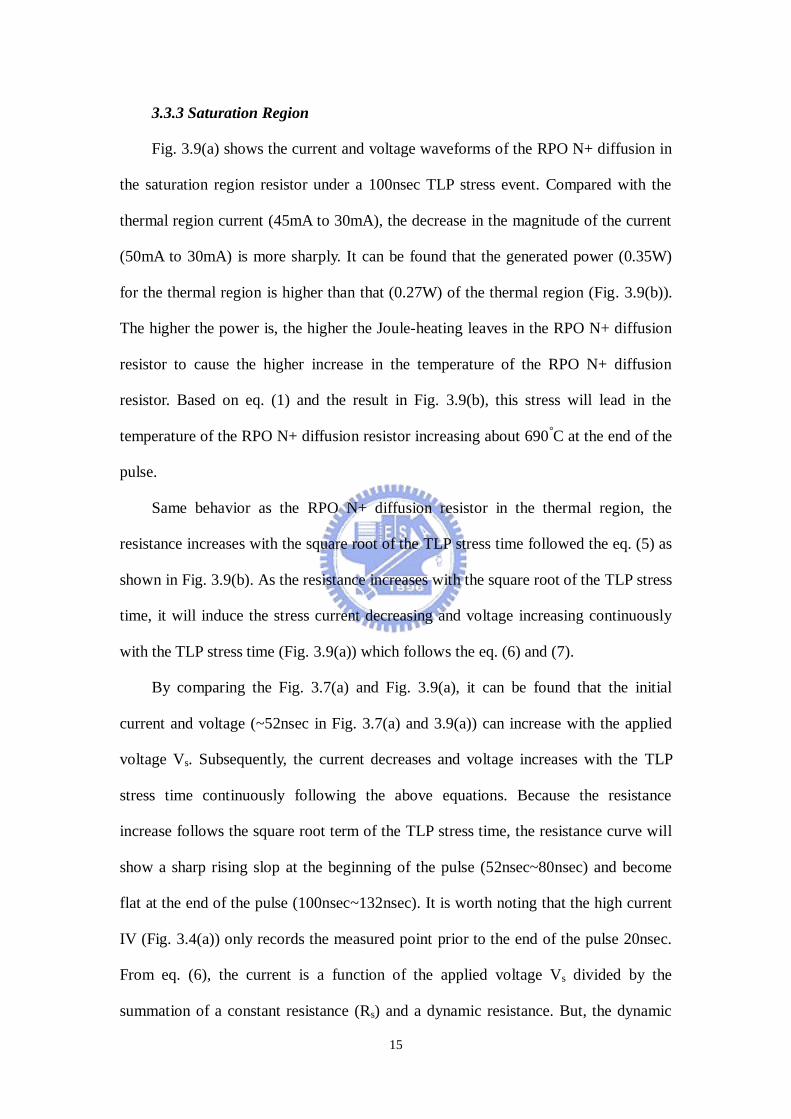
15
333 Saturation Region
Fig 39(a) shows the current and voltage waveforms of the RPO N+ diffusion in
the saturation region resistor under a 100nsec TLP stress event Compared with the
thermal region current (45mA to 30mA) the decrease in the magnitude of the current
(50mA to 30mA) is more sharply It can be found that the generated power (035W)
for the thermal region is higher than that (027W) of the thermal region (Fig 39(b))
The higher the power is the higher the Joule-heating leaves in the RPO N+ diffusion
resistor to cause the higher increase in the temperature of the RPO N+ diffusion
resistor Based on eq (1) and the result in Fig 39(b) this stress will lead in the
temperature of the RPO N+ diffusion resistor increasing about 690degC at the end of the
pulse
Same behavior as the RPO N+ diffusion resistor in the thermal region the
resistance increases with the square root of the TLP stress time followed the eq (5) as
shown in Fig 39(b) As the resistance increases with the square root of the TLP stress
time it will induce the stress current decreasing and voltage increasing continuously
with the TLP stress time (Fig 39(a)) which follows the eq (6) and (7)
By comparing the Fig 37(a) and Fig 39(a) it can be found that the initial
current and voltage (~52nsec in Fig 37(a) and 39(a)) can increase with the applied
voltage Vs Subsequently the current decreases and voltage increases with the TLP
stress time continuously following the above equations Because the resistance
increase follows the square root term of the TLP stress time the resistance curve will
show a sharp rising slop at the beginning of the pulse (52nsec~80nsec) and become
flat at the end of the pulse (100nsec~132nsec) It is worth noting that the high current
IV (Fig 34(a)) only records the measured point prior to the end of the pulse 20nsec
From eq (6) the current is a function of the applied voltage Vs divided by the
summation of a constant resistance (Rs) and a dynamic resistance But the dynamic
16
resistance is a function of the applied voltage based on eqs (1) and (4) and can be
expressed as
))(1()( 2
00
2
0 RRtRkVRtR SS (8)
At the beginning of the stress pulse the second term is small and can be
neglected So the stress current still increases with the applied voltage As the stress
time is long enough the second term of eq (8) becomes important It can compensate
the increase in the current caused by the applied voltage resulting in the current
independent of the applied voltage So the stress voltage still can increase with stress
voltage but the stress current will be clamped to a constant for the longer time stress
This is why the high current IV (Fig 34) shows that the current cannot be increased
at the saturation region If the recording data point is at other region the high current
IV curve of the RPO N+ diffusion resistor will not appear the saturation characteristic
334 Snapback Region
Fig 310(a) shows the current and voltage waveforms of the RPO N+ diffusion
resistor in the snapback region under a 100nsec TLP stress event For this stress the
applied voltage (~9V) in the initial transient (50nsec~95nsec) is apparently higher
than the breakdown voltage of the N+ diffusion 85V based on the DC IV measured
result in Fig 35 Unlike the stress currents of the linear region thermal region and
saturation region the current of the snapback region cannot be confined in the RPO
N+ diffusion resistor any more Most of the current still flows through the RPO N+
diffusion resistor but part of the current flows into the P-substrate and through the
P-Well resistor (R-sub) to Vss (Fig 311(a)) This gives rise of the substrate potential
as shown in Fig 312 In this test structure a floating P+ pick-up (Fig 22) is
designed to monitor the P-substrate potential variation of the RPO N+ diffusion
17
resistor during the TLP stress period The set-up for substrate potential is shown in
Fig 23
Like the behavior of the thermal region and saturation region the RPO N+
diffusion resistor resistance increases with the stress time caused by the RPO N+
diffusion resistor temperature increasing due to power induced the Joule-heating
generation (Fig 312) The increase in the RPO N+ diffusion resistor resistance will
decrease the current flowing through the RPO N+ diffusion resistor to push more
current flowing into the P-substrate resulting in the substrate potential increasing
gradually as shown in Fig 312 (50nsec~95nsec) As the substrate potential reaches
the critical point (07V at the stress time 95nsec in Fig 312) the junction between the
P-substrate and the cathode of the RPO N+ diffusion resistor will be forwarded
resulting in the cathode of the RPO N+ diffusion resistor injecting the electrons
These injected electrons will be collected by the anode of the RPO N+ diffusion
resistor This action can be treated as the npn bipolar turned on (Fig 311(b)) As the
npn bipolar turned on it can provide a very low impedance conduction path to sink
much more than the current that the RPO N+ diffusion resistor can sink The resistor
during the snapback region can be treated as a RPO N+ diffusion resistor and on
resistor of an npn bipolar in parallel But the on resistor resistance of an npn bipolar
is much smaller than the RPO N+ diffusion resistor resistance We can find the
resistance during the snapback region is apparently is much smaller than that of the
region before occurred the snapback This induces the current increasing and voltage
decreasing drastically So an apparent snapback phenomenon can be found after the
transient 95nsec in Fig 311(a) Then a lot of current will flow though the P-substrate
to result in the substrate potential at region B in Fig 311 increases sharply
18
34 High Current IV Characteristic For Silicided N+ Diffusion
Resistor
Fig 313 shows the high current I-V characteristics of a silicided N+ diffusion
resistor under the 100nsec TLP stress event The set-up is shown in Fig 23 A
100nsec current pulse is applied to one node of the silicided N+ diffusion resistor (A
in Fig 23) with respective to the grounded node of the silicided N+ diffusion resistor
and P-substrate (C in Fig 23) The stress current level is increased continuously until
the silicided N+ diffusion resistor was damaged The voltage and current waveforms
of the silicided N+ diffusion resistor during the TLP stress period are measured
simultaneously by the oscillator-scope After each TLP stress a DC meter is used to
check the variation of the leakage current of the silicided N+ diffusion resistor for
judging whether the silicided N+ diffusion resistor was damaged by the TLP stress or
not All measured datarsquos are transferred to a computer by an IEEE-488 cable The
computer records the data at 20nsec prior to the end of the TLP pulse and leakage
current to the disk Based on the recorded values at each stress level the high current
IV characteristics of the device are constructed as shown in Fig 313
Although the high current IV characteristics of the silicided N+ diffusion resistor
also can be divided by four regions it does not be found the snapback phenomenon
even at high current stress level The four regions for silicided N+ diffusion resistor
are linear region thermal region saturation region and breakdown region For linear
region the current increases with the voltage linearly Compared with the linear
region the rising slop of the current at the thermal region is more gradient As it goes
into the saturation region the current cannot increase with the voltage any more It is
worth noting that the saturation current for silicided N+ diffusion resistor (135mA) is
larger than that of the RPO N+ diffusion resistor (33mA) since the silicided N+
diffusion resistor includes two conduction layers (silicided film and N+ diffusion) and
19
the current conduction capability of silicided film is higher than that of RPO N+
diffusion
Unlike the RPO N+ diffusion resistor that can be driven into the snapback when
the applied voltage higher than the junction avalanche breakdown voltage the current
for the silicided N+ diffusion resistor still can be kept as a constant even the applied
voltage higher than the junction avalanche breakdown voltage (85V as shown in Fig
35) This difference is caused by that the two test structures have different P+
diffusion layouts For RPO N+ diffusion resistor the P+ diffusion used as the ground
is below the cathode of the RPO N+ diffusion resistor (Fig 22) For silicided N+
diffusion resistor the P+ diffusion used as the ground is a guard-ring which surrounds
the silicided N+ diffusion resistor completely This kind layout will decrease the
resistance of the substrate resistor (Rsub in Fig 311(a)) significantly to result in the
turn-on condition for a bipolar (IsubtimesRsub) hard to achieve So the snapback
phenomenon cannot be found and the silicided N+ diffusion resistor only can be
biased at avalanche region if the applied voltage is higher than the junction
breakdown voltage
35 Real-Time IV Characteristic For Silicided N+ Diffusion Resistor
Same reason as we talked in the RPO N+ diffusion resistor a single recoding
point IV can not tell us whatrsquos going on of the silicided N+ diffusion resistor during
the TLP stress event So the whole voltage and current waveform are used to
investigate the detail insight of a silicided N+ diffusion resistor under the TLP stress
event
20
351 Linear Region
Fig 314(a) shows the current and voltage waveforms of the silicided N+
diffusion resistor in the linear region under a 100nsec TLP stress event From 25nsec
to 52nsec the pulse travels through the measured probes to the silicided N+ diffusion
resistor and bounces back to the measured probes (Fig 23) At this period the
voltage and current are the constants Compared the Fig 36(a) and Fig 314(a) the
voltage waveform of the silicided N+ diffusion resistor during the TLP stress period is
apparently different from that of the RPO N+ diffusion resistor during the TLP stress
period It is because of that the resistance of the silicided N+ diffusion resistor (~30Ω)
is smaller than the TLP output resistance (50Ω) but the resistance of the RPO N+
diffusion resistor (~170Ω) is much larger than the TLP output resistance (50Ω)
Except the resistor resistance the inductance caused by the bonding wire or probe is
needed to count into the impedance for the loading (ZL) But it is well known that the
impedance caused by the inductance is arisen from LdIdt So it only can affect the
voltage waveform at the beginning of the TLP stress due to large dIdt (B in Fig
314(a)) but can be neglected after this transient due to nearly zero dIdt
Adding the inductance will cause the loading impedance ZL larger than the TLP
output resistance to generate a positive reflected wave based on the formula
Γ=(ZL-Z0)(ZL+Z0) resulting in the voltage higher than the initial voltage (Vi in Fig
314(a)) Without the inductance the impedance of the silicided N+ diffusion resistor
becomes smaller than the TLP output resistance to induce a negative reflected
waveform resulting in the voltage smaller than the initial voltage (Vi in Fig 314(a))
Based on the measured voltage and current in Fig 314(a) the dynamic
resistance (V(t)I(t)) and the generated power (V(t)timesI(t)) can be obtained as shown in
Fig 314(b) It can be found that the resistance and the generated power all can keep
as the constants during the TLP stress period since the Joule-heating generated by the
21
power is still quite low and all can be transferred into the substrate completely
Without the additional heat the silicided N+ diffusion resistor temperature does not
vary with the TLP stress time and the resistance can keep as the constant based on eq
(1) So the current of the silicided N+ diffusion resistor can linearly increase with the
voltage as it is biased at the linear region
352 Thermal Region
Fig 315(a) shows the current and voltage waveforms of the silicided N+
diffusion resistor in the thermal region under a 100nsec TLP stress event It can be
found that the current decreases and the voltage increases continuously during the
TLP stress period Based on the measured voltage and current in Fig 315(a) the
dynamic resistance (V(t)I(t)) and the generated power (V(t)timesI(t)) can be obtained as
shown in Fig 315(b) It can be found that the resistance increases with the TLP stress
time and the generated power is nearly a constant during the TLP stress period Same
mechanism as the discussion in the thermal region for RPO N+ diffusion resistor the
P-substrate can not sink all Joule-heating generated from the power in an instant to
leave part of Joule-heating in the silicided N+ diffusion resistor resulting in the
increase in the temperature of the silicided N+ diffusion resistor The detail
mechanism that the current and voltage varied with the TLP stress time had been
discussion in the section of the thermal region for RPO N+ diffusion resistor Based
on eq(1) and the result in Fig 315(b) this stress will lead in the temperature of the
silicided N+ diffusion resistor increasing about 139degC Compared with the RPO N+
diffusion resistor the temperature increase at the thermal region for the silicided N+
diffusion resistor is nearly 13 of the temperature increase for the RPO N+ diffusion
resistor since the temperature coefficient of the silicided N+ diffusion resistor is
nearly three times of the RPO N+ diffusion resistor
22
353 Saturation Region
Fig 316(a) shows the saturation region current and voltage waveforms of the
silicided N+ diffusion resistor under a 100nsec TLP stress event Compared with the
current in the thermal region (108mA to 99mA) the saturation current decreases more
sharply (148mA to 113mA) The generated power (~1W) during the saturation region
(Fig 316(b)) is nearly twice of the generated power (05W) during the thermal region
(Fig 315(b)) The more power is generated the more Joule-heating leaves in the
silicided N+ diffusion resistor to induce in the higher temperature for the silicided N+
diffusion resistor Based on eq (1) and the result in Fig 316(b) this stress will lead
the temperature of the silicided N+ diffusion resistor increasing about 224degC at the
end of the pulse which is much higher than the increase in the temperature of the
silicided N+ diffusion resistor during the thermal region (139degC) but much smaller
than the increase in the temperature of the RPO N+ diffusion resistor during the
saturation region (690degC) Fig 316(b) shows that the silicided N+ diffusion resistor
also can follow eq (6) which resistance increases with the square root of the stress
time Thus the current and voltage also can follow the eqs (7) and (8) to increase and
decrease with the stress time respectively By comparing Figs 37(b) and 15(b) or
Figs 39(b) and 16(b) it can be found that the generated power for silicided N+
diffusion resistor during the TLP stress period is nearly a constant that does not vary
with the stress time while the generated power for the RPO N+ diffusion resistor
during the TLP stress period decreases with the stress time It implies that the thermal
conduction for RPO N+ diffusion resistor is better than the silicided N+ diffusion
resistor The more heat transferred into the P-substrate the less power left in the RPO
N+ diffusion resistor So the generated power will decrease with the stress time The
less heat transferred into the P-substrate the more power left in the silicided N+
diffusion resistor So the generated power does not vary with the stress time This
23
difference might be caused by that the current of the silicided N+ diffusion resistor is
confined in the thin silicided film to induce the local heating but the current of RPO
N+ diffusion resistor can flow whole junction and the junction is just above the large
heat-sink P-substrate Because the Joule-heating induced the device temperature
increasing higher than the silicon melting point is the main cause of the ESD failure
the device will have poor ESD performance if it has the bad thermal conductivity
This is why we often think that the silicided process will degrade the device ESD
performance
36 ESD Comparison For Silicided And RPO Grounded-Gate NMOS
The self-protection scheme which NPMOS drivers are the ESD protection
devices is commonly used for digital IO ESD protection Using this scheme the
NMOS will dominate the ESD event So NMOS is much more important than the
PMOS for IO ESD protection in CMOS technology Up to now ESD designers often
have the concept that the silicided process will degrade the device ESD performance
So various schemes from process (silicided block (RPO) [6]) and circuits (gate
coupling [7] and substrate trigger [8]) are proposed to improve the NMOS ESD
performance But the RPO scheme seems more popular than other schemes since
most foundries provide the RPO design rules for customers as the reference And
most ESD designers accept the concept that RPO can build a ballast resistor [9] for
NMOS But most people do not know why NMOS needs a ballast resistor drain In
fact the ESD event can be treated as a constant current stress event Whether the
device has a ballast resistor cannot change the ESD stress current level [10] and the
current capability of the silicided N+ diffusion resistor is apparently much higher than
that of the RPO N+ diffusion resistor from above experiment result If the silicided
24
N+ diffusion resistor can sustain more current than the RPO N+ diffusion resistor it
does not have the reason that the silicided device is more vulnerable to ESD stress
than the RPO device So the ballast resistor concept cannot explain why using RPO
to forbid the silicided formation on the drain can improve the device ESD
performance In fact we find the silicided device can be designed as robust as or even
better than the RPO device
As we discussed in the above sections we can conclude some different
characteristics for RPO N+ diffusion resistor and silicided N+ diffusion resistor 1
the thermal conductivity of the RPO N+ diffusion resistor is better than the silicided
N+ diffusion resistor 2 the saturation current of the silicided N+ diffusion resistor is
higher than that of RPO N+ diffusion resistor 3 for silicided N+ diffusion resistor
most current will be confined in the silicided film 4 for RPO N+ diffusion resistor
the current can distribute whole junction Because of these different behaviors the
silicided grounded-gate NMOS (GGNMOS) and RPO GGNMOS cannot use same
kind layout if one wants to get good ESD performance for these two devices
Fig 24 shows the layouts of these two devices Table 31 lists the key
parameters and ESD test results for these two devices The dimensions for these two
devices are almost the same (silicided GGNMOS 30times336=1008um2 RPO GGNMOS
30times3395=10185um2) Based on characteristic 4 the current of the RPO N+ diffusion
resistor can distribute whole junction we use long contact to poly space on the drain
(RPO=16um) to get larger drain junction (436times30times5=654um2) compare with the
silicided device (096times30times12=3456um2) Based on characteristic 3 most current of
the silicided N+ diffusion resistor will be confined in the silicided film the junction is
useless for the silicided device ESD protection So we need to increase total drain
junction perimeter of the silicided device instead of using larger device drain junction
area as the RPO device since most current flows from contact through LDD junction
25
to P-substrate The total perimeter of the drain junction for the silicided GGNMOS
(30times12times2=720um) is nearly two and a half of the RPO GGNMOS (30times5times2=300um)
Based on above design concept both devices all can get better ESD
performances that can pass HBM 2KV and MM 200V industry specification (Table
31) And it is worth noting that ESD performance of the silicided GGNMOS is more
robust than the RPO GGNMOS For the silicided GGNMOS it can pass HBM 75KV
MM 350V and It2 335A For the RPO GGNMOS it can pass HBM 55KV MM
250V and It2 25A Fig 317 shows the high current IV characteristics of the silicided
GGNMOS and RPO GGNMOS It can be found that the silicided GGNMOS has
smaller Ron and higher It2 compared with the RPO GGNMOS For same dimension
the ESD performance for the silicided GGNMOS can be designed higher than 30 of
the RPO GGNMOS in 025um CMOS process The comparison of silicided and
non-silicided GGNMOS in series with a resistor between gate and ground is the future
work in other process
26
Table 31 Key layout parameter and ESD test result
Stru Length Finger
Width
Total
Width
Cont-
to-
Poly
RPO-to-
Poly
at Drain
Poly-to
-Poly
at Drain
Total
DrainSource
OD Area
HBM MM It2
Silicided 04um 30um 720um 03um NA 096um 1008um2 75kV 350V 335A
RPO 04um 30um 300um 20um 16um 436um 1018um2 55kV 250V 25A
27
000 002 004 006 008 010000
005
010
015
020
025
030
035
040
045
050
055
060RPO N+ Diffusion (WL=2um3um)
Cu
rre
nt
(mA
)
Volatge (V)
25oC
75oC
125oC
(a)
20 40 60 80 100 120 140170
175
180
185
190
195RPO N+ Diffusion (WL=2um3um)
Re
sis
tan
ce
(o
hm
)
Temperature (oC)
(b)
Fig 31 (a) DC IV Characteristics of a RPO N+ diffusion resistor vs temperature (b)
Resistance vs temperature
28
000 002 004 006 008 01000
05
10
15
20
25
30
C
urr
en
t (m
A)
Volatge (V)
Silicided N+ Diffusion (WL=2um165um)
25oC
75oC
125oC
(a)
20 40 60 80 100 120 14030
32
34
36
38
40
42
Re
sis
tan
ce
(o
hm
)
Temperature (oC)
Silicided N+ Diffusion (WL=2um165um)
(b)
Fig 32 (a) DC IV Characteristics of a Silicided N+ diffusion resistor vs temperature
(b) Resistance vs temperature
29
(a)
(b)
Fig 33 (a) Silicided N+ diffusion resistor has two conductor layers (silicided film
and N+ diffusion) (b) RPO N+ diffusion resistor only has one conductor layer (N+
diffusion)
30
000
002
004
006
008
010
012
014
016
018
020
0 1 2 3 4 5 6 7 8 9
Leakage 05V
Silicide_block N+ diffusion (WL=2um3um)
Cu
rre
nt
(A)
Voltage (V)
1E-3 001 01 1
Leakage (A) 05V
(a)
000
001
002
003
004
0 1 2 3 4 5 6 7 8 9
Leakage 05V
Silicide_block N+ diffusion (WL=2um3um)
Cu
rre
nt
(A)
Voltage (V)
1E-3 001 01 1
Leakage (A) 05V
(b)
Fig 34 High current IV Characteristics of a RPO N+ diffusion resistor (a) from linear
region to snapback region (b) from linear region to saturation region
31
0 1 2 3 4 5 6 7 8 9 10
1E-11
1E-10
1E-9
1E-8
1E-7
1E-6
1E-5
Cu
rren
t (A
)
Voltage (V)
RPO N+PW BV
85V0 1 2 3 4 5 6 7 8 9 10
1E-11
1E-10
1E-9
1E-8
1E-7
1E-6
1E-5
Cu
rren
t (A
)
Voltage (V)
RPO N+PW BV
85V
Fig 35 DC IV Characteristics of a RPO N+ diffusion resistor
32
0 50 100 150
00
05
10
15
20
Stress Voltage
Stress Current
Time (ns)
Vo
lta
ge
(V
)
-5
0
5
10
15
20
Cu
rren
t (mA
)
2LV stress
Reflect waveIncidentwave
0 50 100 150
00
05
10
15
20
Stress Voltage
Stress Current
Time (ns)
Vo
lta
ge
(V
)
-5
0
5
10
15
20
Cu
rren
t (mA
)
2LV stress
Reflect waveIncidentwave
(a)
0 50 100 1500
50
100
150
200
250
Power (VI)
R (VI)
Time (ns)
Resis
tan
ce (
oh
m)
0000
0005
0010
0015
0020
0025
0030
Po
wer (W
)
(a)
Fig 36 Linear region
(a) Voltage and Current waveforms (b) Resistance (VI) and power (VtimesI) vs time for
a RPO N+ diffusion resistor under the 100nsec TLP pulse event
33
0 50 100 1500
2
4
6
8
Time ( ns )
Vo
ltag
e (
V )
Meas V
Theoretical V
0
10
20
30
40
50
Cu
rrent ( m
A )
Meas I
Theoretical I
stress
0 50 100 1500
2
4
6
8
Time ( ns )
Vo
ltag
e (
V )
Meas V
Theoretical V
0
10
20
30
40
50
Cu
rrent ( m
A )
Meas I
Theoretical I
stressstress
(a)
50 100 15050
100
150
200
250
Time ( ns )
Re
sis
atn
ce
( o
hm
)
R based meas V and I
Theoretical R
00
01
02
03
04
05
Po
we
r ( W )
Power based on meas V and I
(b)
Fig 37 Thermal region (a) Voltage and Current waveforms (b) Resistance (VI) and
power (VtimesI) vs time for a RPO N+ diffusion resistor under the 100nsec TLP pulse
event
34
Rs(50)
Vs
Vss
R(t)
TLP System
I(t)
V(t)
Rs(50)
Vs
Vss
R(t)
TLP System
I(t)
V(t)
Fig 38 Equivalent circuit of a RPO N+ diffusion resistor under the 100nsec TLP
pulse event
35
0 50 100 1500
2
4
6
8
Time ( ns )
Vo
ltag
e (
V )
Meas V
Theoretical V
0
10
20
30
40
50
60C
urre
nt ( m
A )
Meas I
Theoretical I
(a)
0 50 100 15050
100
150
200
250
300
Time ( ns )
Re
sis
atn
ce
( o
hm
) R based on meas V and I
Theoretical R
00
01
02
03
04
05
06
07
Po
we
r ( W )
Power based on meas V and I
(b)
Fig 39 Saturation region (a) Voltage and Current waveforms (b) Resistance (VI)
and power (VtimesI) vs time for a RPO N+ diffusion resistor under the 100nsec TLP
pulse event
36
0 50 100 1500
1
2
3
4
5
6
7
8
9
10
Vo
ltag
e (
V)
Cu
rren
t (mA
)
Time (ns)
Stress Voltage
Stress Current
0
20
40
60
80
100
120
stress
snapback
0 50 100 1500
1
2
3
4
5
6
7
8
9
10
Vo
ltag
e (
V)
Cu
rren
t (mA
)
Time (ns)
Stress Voltage
Stress Current
0
20
40
60
80
100
120
stress
snapback
(a)
0 50 100 150
50
100
150
200
250
R (VI)
Power (VI)
00
01
02
03
04
05
06
07
Po
wer (W
)
Time (ns)
Re
sis
tan
ce (
oh
m)
snapback
0 50 100 150
50
100
150
200
250
R (VI)
Power (VI)
00
01
02
03
04
05
06
07
Po
wer (W
)
Time (ns)
Re
sis
tan
ce (
oh
m)
snapback
(b)
Fig 310 Snapback region (a) Voltage and Current waveforms (b) Resistance (VI)
and power (VtimesI) vs time for a RPO N+ diffusion resistor under the 100nsec TLP
pulse event
37
(a)
(b)
Fig 311 The current (a) before the snapback region (b) at the snapback region
0 50 100 15000
05
10
15
20
25
Vo
lta
ge
(V)
Time(ns)
Substrate potential
snapback
0 50 100 15000
05
10
15
20
25
Vo
lta
ge
(V)
Time(ns)
Substrate potential
snapback
Fig 312 The measured substrate potential (B in Fig 311) for the stress in Fig 310
38
000
005
010
015
020
025
030
0 2 4 6 8 10 12 14 16 18
Leakage 05V
Silicide N+ diffusion (WL 2165)
Cu
rren
t (A
)
Voltage (V)
001 01 1 10 100 1000
Leakage (A) 05V
A (linear region)
B (thermal region)
C (saturation region)
D (breakdown region)
000
005
010
015
020
025
030
0 2 4 6 8 10 12 14 16 18
Leakage 05V
Silicide N+ diffusion (WL 2165)
Cu
rren
t (A
)
Voltage (V)
001 01 1 10 100 1000
Leakage (A) 05V
A (linear region)
B (thermal region)
C (saturation region)
D (breakdown region)
(a)
000
002
004
006
008
010
012
014
016
0 2 4 6 8 10 12 14
Leakage 05V Silicided N+ diffusion (WL 2165)
Cu
rre
nt
(A)
Voltage (V)
001 01 1 10 100 1000
Leakage (A) 05V
A
(linear region)
B (thermal region)
C (saturation region)000
002
004
006
008
010
012
014
016
0 2 4 6 8 10 12 14
Leakage 05V Silicided N+ diffusion (WL 2165)
Cu
rre
nt
(A)
Voltage (V)
001 01 1 10 100 1000
Leakage (A) 05V
A
(linear region)
B (thermal region)
C (saturation region)
(b)
Fig 313 (a) High current IV Characteristics of a Silicided N+ diffusion resistor (b)
Zoom-In
39
(a)
0 50 100 1500
10
20
30
40
50
Resis
tan
ce
(o
hm
)P
ow
er (W
)
R (VI)
Power (VI)
Time (nsec)
0000
0005
0010
0015
0020
0025
0030
0 50 100 15000
05
10
15
20
Stress Voltage
Stress Current
Time (ns)
Vo
ltag
e (
V)
0
5
10
15
20
Cu
rren
t (mA
)
0 50 100 1500
10
20
30
40
50
Resis
tan
ce
(o
hm
)P
ow
er (W
)
R (VI)
Power (VI)
Time (nsec)
0000
0005
0010
0015
0020
0025
0030
0 50 100 15000
05
10
15
20
Stress Voltage
Stress Current
Time (ns)
Vo
ltag
e (
V)
0
5
10
15
20
Cu
rren
t (mA
)
(b)
Fig 314 Linear region
(a) Voltage and Current waveforms (b) Resistance (VI) and power (VtimesI) vs time for
a silicided N+ diffusion resistor under the 100ns pulse event
40
0 50 100 150
0
1
2
3
4
5
6
Vo
ltag
e (
V)
Cu
rren
t (mA
)
Time (nsec)
Stress Current
Stress Voltage
0
20
40
60
80
100
stress
0 50 100 150
0
1
2
3
4
5
6
Vo
ltag
e (
V)
Cu
rren
t (mA
)
Time (nsec)
Stress Current
Stress Voltage
0
20
40
60
80
100
stress
0 50 100 15000
05
10
15
20
Stress Voltage
Stress Current
Time (ns)
Vo
ltag
e (
V)
0
5
10
15
20
Cu
rren
t (mA
)
0 50 100 150
0
1
2
3
4
5
6
Vo
ltag
e (
V)
Cu
rren
t (mA
)
Time (nsec)
Stress Current
Stress Voltage
0
20
40
60
80
100
stress
0 50 100 150
0
1
2
3
4
5
6
Vo
ltag
e (
V)
Cu
rren
t (mA
)
Time (nsec)
Stress Current
Stress Voltage
0
20
40
60
80
100
stress
0 50 100 15000
05
10
15
20
Stress Voltage
Stress Current
Time (ns)
Vo
ltag
e (
V)
0
5
10
15
20
Cu
rren
t (mA
)
(a)
0 50 100 150
35
40
45
50
55
60
Power (VI)
Resis
atn
ce (
oh
m )
Time ( ns )
R (VI)
02
03
04
05
06
Po
wer ( W
)
(b)
Fig 315 Thermal region (a) Voltage and Current waveforms (b) Resistance (VI)
and power (VtimesI) vs time for a silicided N+ diffusion resistor under the 100nsec TLP
pulse event
41
0 50 100 1500
1
2
3
4
5
6
7
8
9
Stress Current
Stress Voltage
0
50
100
150
Vo
lta
ge
(V
)
Time (nsec)
Cu
rren
t (mA
)
stress
0 50 100 1500
1
2
3
4
5
6
7
8
9
Stress Current
Stress Voltage
0
50
100
150
Vo
lta
ge
(V
)
Time (nsec)
Cu
rren
t (mA
)
stress
0 50 100 15000
05
10
15
20
Stress Voltage
Stress Current
Time (ns)
Vo
ltag
e (
V)
0
5
10
15
20
Cu
rren
t (mA
)
0 50 100 1500
1
2
3
4
5
6
7
8
9
Stress Current
Stress Voltage
0
50
100
150
Vo
lta
ge
(V
)
Time (nsec)
Cu
rren
t (mA
)
stress
0 50 100 1500
1
2
3
4
5
6
7
8
9
Stress Current
Stress Voltage
0
50
100
150
Vo
lta
ge
(V
)
Time (nsec)
Cu
rren
t (mA
)
stress
0 50 100 15000
05
10
15
20
Stress Voltage
Stress Current
Time (ns)
Vo
ltag
e (
V)
0
5
10
15
20
Cu
rren
t (mA
)
(a)
0 50 100 15030
35
40
45
50
55
60
65
R
es
isa
tnc
e (
oh
m )
Time ( ns )
meas R (VI)
cal R based on eq (6)
Power (VI)
00
02
04
06
08
10
Po
we
r ( W )
(b)
Fig 316 Saturation region (a) Voltage and Current waveforms (b) Resistance (VI)
and power (VtimesI) vs time for a silicided N+ diffusion resistor under the 100nsec TLP
pulse event
42
00020406081012141618202224262830323436
0 1 2 3 4 5 6 7 8 9 10
Silicide GGNMOSRPO GGNMOS
Cu
rren
t (A
)
Voltage (V)
1E-111E-101E-9 1E-8 1E-7 1E-6 1E-5 1E-4 1E-3 001 01 1
Leakage (A) 363V
00020406081012141618202224262830323436
00020406081012141618202224262830323436
0 1 2 3 4 5 6 7 8 9 10
Silicide GGNMOSRPO GGNMOS
Cu
rren
t (A
)
Voltage (V)
1E-111E-101E-9 1E-8 1E-7 1E-6 1E-5 1E-4 1E-3 001 01 1
Leakage (A) 363V
Fig 317 High current IV characteristics of (a) silicided GGNMOS
(WL=720um04um) (b) RPO GGNMOS (WL=300um04um)
43
Chapter 4
Applications for On-chip ESD Protection Design
Up to now there are many kinds of ESD protect devices in IC chip The devices
include diode GGNMOS SCR diffusion resistor and so on Specially the diffusion
resistor can be used to incorporated with ESD protect devices to enhance the chip
ESD level and it does not cost too much area There are different considerations about
input and output buffer
41 Input Pin ESD Protection Improvement
For input pads the typical ESD protection device grounded-gate NMOS
(GGNMOS) often can pass over HBM 2KV And the manufacture Fab usually
provides additional process ESD implant to enhance the device ESD performance
and does not affect the IC function To prevent the gate oxide damage it often needs a
resistor in series with a 2nd
ESD protection device before an inverter gate However it
is never discussed how to design the resistor and 2nd
ESD protection before From the
high current IV characteristics of the resistor under a TLP stress in above chapter it
provides us a guide line to design the resistor and 2nd
ESD protection device The
guide line is that the saturation current of a resistor should be designed smaller than
the It2 of the 2nd
ESD protection device This can make sure that the 2nd
ESD
protection cannot be damaged by the ESD and 2nd
ESD protection can be turned on to
clamp the ESD voltage in an instant to prevent gate oxide damage Otherwise the 2nd
ESD protection might be damaged before the primary turned on since the current
44
cannot be clamped below the current of the 2nd
ESD protection that can sustain This
will degrade the input pad ESD performance
It has been proven that the input pad HBM passing voltage can be improved
from 3KV to 5KV after inserting 200Ω poly resistor at MCU (Micro Controlled Unit)
product About the diffusion resistor effect on ESD performance has been reported
[11] This report shows how to use diffusion resistor to improve low trigger voltage
and low capacitance ESD protection device (LVCESD) for high frequency input pad
The LVCESD structure is shown in the Fig 41 and the test result of the resistor and
trigger device of LVCESD is shown in table 41 From the TLP curve in Fig 42 the
saturation current of a P+ diffusion resistor is designed lower than the It2 of NMOS
This can prevent the trigger device damage Compared with the structure without the
P+ diffusion resistor the LVCESD with a P+ diffusion resistor has much robust ESD
performance In this report it has another experiment to study how the diffusion
resistor to incorporate with the LVCESD to protect the inverter gate and output
transistor This experiment shows that LVCESD cannot effectively protect the
inverter gate and output transistor if it is without a resistor before the protected device
The structures show in the Fig 43 and the ESD results are listed in the table 42 For
input ESD protection the ESD performance can be improved significantly (HBM
15KV to 55KV and MM 50V to 400V) if it has a resistor and 2nd
ESD protection
device
42 Output Pin ESD Protection Improvement
Unlike input pad which needs to add a protection device between the pad and
the input gate the output buffer is already an ESD protection device usually And it is
hard to optimize the output transistor layout to meet both circuit requirement and ESD
45
performance For ESD consideration it often uses the larger contact to gate space to
build a ballast resistor for the output transistor For circuit performance however it
cannot use the large contact to poly space since it will increase the RC delay time to
reduce the IO speed and increase the noise level In addition this scheme has the
severe impact on the size and performance of the output buffer especially the pad
limitation becomes a major design constraint It had been reported that a modified
output structure adding a small resistor has significantly improved the ESD
performance recently Taking the advantage of the velocity saturation at high current
a resistor is a low impedance resistance at normal operation (Idclt15mA) while
becomes a high impedance resistor at the high current ESD zapping event (hundreds
of mArsquos to Arsquos) To meet the speed requirement at normal operation and prevent the
output transistor damage during the ESD zapping the resistance of a resistor is
limited below 10Ω and the Isatv should be designed smaller than the It2 of the output
transistor Using the data presented in Figs 44 and 45 either the n+ diffusion
resistor (WL=15um4um) or the n-well resistor (WL=350um15um) can satisfy
these requirements However the heavily doped resistor may not be a good candidate
due to too small Vsat Note that the actual selection of Isat and Rs should be further
optimized by design layout and technology constraints With such optimization the
ESD current (for 2KV using the HBM the peak current Ip is about 13A) will be
discharged either through a specially designed protection structure (Fig 46(a)) or the
leakage current caused by breakdown between the Vcc and Vss lines (Fig 46(b)) This
will allow the use of the aggressive design rules of the technology rather than the
conservative channel length and poly gate to diffusion contact spacing resulting in
better ESD performance and only a minor compromise in the IO area
46
Table 41 LVCESD structure device splits ESD test result
Structure A B
+HBMVss 2kV 5kV
-HBMVss -65kV -60kV
+HBMVcc 3kV 5kV
-HBMVcc -45kV -45kV
+MMVss 100V 350V
-MMVss -400V -400V
+MMVcc 75V 350V
-MMVcc -300V -350V
Structure A B
+HBMVss 2kV 5kV
-HBMVss -65kV -60kV
+HBMVcc 3kV 5kV
-HBMVcc -45kV -45kV
+MMVss 100V 350V
-MMVss -400V -400V
+MMVcc 75V 350V
-MMVcc -300V -350V
Table 42 LVCESD structure with chip splits ESD test result
Stru I II III IV
HBM (+Vss) +15kV +25kV +025kV + 55kV
HBM (-Vss) -60kV -60kV -65kV -60kV
HBM (+Vcc) +15kV +25kV +025kV +50kV
HBM (-Vcc) -15kV -15kV -20kV -30kV
MM (+Vss) +50V +100V lt25V +400V
MM (-Vss) -400V -400V -425V -400V
MM (+Vcc) +75V +100V +25V +375V
MM (-Vcc) -100V -75V -125V -400V
Stru I II III IV
HBM (+Vss) +15kV +25kV +025kV + 55kV
HBM (-Vss) -60kV -60kV -65kV -60kV
HBM (+Vcc) +15kV +25kV +025kV +50kV
HBM (-Vcc) -15kV -15kV -20kV -30kV
MM (+Vss) +50V +100V lt25V +400V
MM (-Vss) -400V -400V -425V -400V
MM (+Vcc) +75V +100V +25V +375V
MM (-Vcc) -100V -75V -125V -400V
47
P+
NW
N+_NW
D1
P+ G
ua
rd
-R
in
g
N+ G
ua
rd
-R
in
g
Vss
Vcc
Asymmetry
NMOS
D2
D1
N+_NW
P+ strap
P+ strap
(a)
PAD
N+
P-substrateSCR
Vss
N+ P+P+
NWD3
pnp
npn2
npn1
Rsub
D1
N+
Vcc
D2
NMOS
(trigger
source)
(b)
Fig 41 Low trigger Voltage and low Capacitance ESD protection device (LVCESD)
(a) top view (b) cross-section
48
Structure A
RPORPO
RPO Silicide Block
Structure B
RPORPO
RPO P+ di f fus ion R
(a)
0 2 4 6 8
00
05
10
15
20
25
30 Structure A
Structure B
Cu
rre
nt ( A
)
Voltage ( V )
Vt1(stru A amp B)
It-2(stru B)
It-2(stru A)
(b)
Fig 42 LVCESD splits (a) split structure (b) TLP curve comparison
49
InputPad
Vs s
Vc c
LVC
ESD
Stru I
InputPad
Vs s
Vc c
LVC
ESD
InputPad
Vs s
Vc c
LVC
ESD
Stru I
InputPad
Rs=10Ω
Vs s
Vc c
LVC
ESD
Stru II
InputPad
Rs=10Ω
Vs s
Vc c
LVC
ESD
InputPad
Rs=10Ω
Vs s
Vc c
LVC
ESD
Stru II
(a) (b)
InputPad
Vs s
Vc c
LVC
ESD
2nd ESD
Stru III
InputPad
Vs s
Vc c
LVC
ESD
2nd ESD
InputPad
Vs s
Vc c
LVC
ESD
2nd ESD
Stru III
I n p u tP a d
Rs= 1 0Ω
Vs s
Vc c
LVC
ESD
2nd ESD
Stru IV
InputPad
Rs=10Ω
Vs s
Vc c
LVC
ESD
2nd ESD
InputPad
Rs=10Ω
Vs s
Vc c
LVC
ESD
InputPad
Rs=10Ω
Vs s
Vc c
LVC
ESD
2nd ESD
Stru IV
(c) (d)
Fig 43 LVCESD splits structure (a) LVCESD (b) LVCESD with 10Ω N+ poly
resistor (c) LVCESD with 2nd
ESD (Silicided NMOS WL=20um025um) (d)
LVCESD with 2nd
ESD (Silicided NMOS WL=20um025um) and 10Ω N+ poly
resistor
(a) (b)
Fig 44 IV characteristics of a n+ diffusion resistor (WL=5um60um) (a) Cathode
and substrate(1) current vs anode-to-cathode voltage with the reverse-bias
characteristics of the same well-substrate diode(2) added for reference (b) The related
static (Rs) and dynamic (Rd) resistance vs anode-to-cathode voltage
50
(a) (b)
Fig 45 IV characteristics of a n-well diffusion resistor (WL=70um14um) (a)
Cathode and substrate current vs anode-to-cathode voltage (b) The related static (Rs)
and dynamic (Rd) resistance vs anode-to-cathode voltage
OutputPad
N1
N2
Rs
Vss
Vcc
Ou tp u tP a d
N2
Rs
Vss
Vcc
(a) (b)
Fig 46 Output buffer with a ldquodecouple resistorrdquo (a) Main discharge through a
protection device N1 (b) Main discharge via the p-source to Vcc diode and the
equivalent discharge path N2 between the Vcc and Vss lines
51
Chapter 5
Conclusions
We had demonstrated that the resistance increases with the square root of the
stress time for both silicided N+ diffusion resistor and RPO N+ diffusion resistor
during the 100nsec high current TLP stress event So the resistor during the high
current stress event will become a dynamic resistance resistor The high current IV
curve provided by the commercial 100nsec TLP system cannot reflect the high current
behavior of the resistor during the high current stress event since it only records one
single point of the measured waveform In fact the resistors cannot clamp the stress
currents at the beginning of the pulse since Joule-heating generation is too small and
can be neglected at this transient So the stress current is proportional to the applied
voltage at this time
The different characteristics of the two kinds of resistors under the high current
stress event are also found Based on the different characteristics of these two kinds of
resistors we use different layouts to enhance the merit and eliminate the drawback for
the silicided GGNMOS and RPO GGNMOS For the silicided device it needs the
large total drain perimeter but does not needs large area drain junction since the
current confines in the silicided film and flows from the contact through LDD
junction to the substrate While for the RPO device it needs large area drain junction
since the current can flow through whole junction Using the different approach for
different device we demonstrate that both silicided GGNMOS and RPO GGNMOS
can get good ESD performance at the same layout area
52
REFERENCES
[1] G Krieger and P Niles ldquoDiffused resistors characteristics at high current density
levels-analysis and applicationrdquo IEEE Trans Electron Devices vol 36 no 2 pp
416-423 1989
[2] K Banerjee and C Hu ldquoHigh current effects in silicide films for sub-025um
VLSI technologiesrdquo in Proc International Reliability Physics Symposium 1998
pp 284-292
[3] D C Wunsch and R R Bell ldquoDetermination of threshold failure levels of
semiconductor diode and transistors due to pulse voltagerdquo IEEE Trans Nuc Sci
vol 15 no 6 pp 244-259 1970
[4] D K Cheng Field and Wave Electromagnetics second edition Addison-Wesley
New York 1989
[5] P A Juliano and E Rosenbaum ldquoAccurate wafer-level measurement of ESD
protection device turn-on using a modified very fast transmission-line pulse
systemrdquo IEEE Trans Device Mater Reliab vol 1 no 2 pp 95-103 2001
[6] D Krakauer and K Mistry ldquoESD protection in 33V sub-micron silcided CMOS
technologyrdquo in Proc EOSESD Symp 1992 pp 250-257
[7] C Duvvury C Diaz and T Haddock ldquoAchieving uniform nMOS device power
distribution for sub-micron ESD reliabilityrdquo IEEE International Electron
Devices Meeting Tech Digest 1992 pp 131-134
[8] A Amerasekera C Duvvury V Reddy and M Rodder ldquoSubstrate triggering
and salicide effects on ESD performance and protection circuit design in deep
submicron CMOS processesrdquo IEEE International Electron Devices Meeting
Tech Digest 1995 pp 547-550
[9] K L Chen ldquoThe effects of interconnect process and snapback voltage on the
ESD failure threshold of NMOS transistorsrdquo IEEE Trans Electron Devices vol
35 no 12 pp 2140-2150 1988
[10] J H Lee J R Shih K F Yu Y H Wu J Y Wu J L Yang C S Hou and T
C Ong ldquoHigh current characteristics of copper interconnect under TLP stress
and ESD zappingrdquo in Proc International Reliability Physics Symposium 2004
pp608-608
[11] J H Lee Y H Wu K F Yu and T C Ong ldquoA low-trigger voltage and
low-capacitance ESD protection device for high frequency applicationsrdquo in
WSEAS Trans Electronics vol 1 no 2 pp231-235 2004
53
VITA
Yao-Wu Feng received his BS degree from EP Dept of Chiao-Tung
University Hsinchu Taiwan in 1997 Now he has been an ESD engineer
of Holtek semiconductor Inc Taiwan He has over 9-year working
experience on semiconductor physics device process and ESD design in
IC industry His research interest includes on-chip ESD protection design
semiconductor devices and IC process

20
351 Linear Region
Fig 314(a) shows the current and voltage waveforms of the silicided N+
diffusion resistor in the linear region under a 100nsec TLP stress event From 25nsec
to 52nsec the pulse travels through the measured probes to the silicided N+ diffusion
resistor and bounces back to the measured probes (Fig 23) At this period the
voltage and current are the constants Compared the Fig 36(a) and Fig 314(a) the
voltage waveform of the silicided N+ diffusion resistor during the TLP stress period is
apparently different from that of the RPO N+ diffusion resistor during the TLP stress
period It is because of that the resistance of the silicided N+ diffusion resistor (~30Ω)
is smaller than the TLP output resistance (50Ω) but the resistance of the RPO N+
diffusion resistor (~170Ω) is much larger than the TLP output resistance (50Ω)
Except the resistor resistance the inductance caused by the bonding wire or probe is
needed to count into the impedance for the loading (ZL) But it is well known that the
impedance caused by the inductance is arisen from LdIdt So it only can affect the
voltage waveform at the beginning of the TLP stress due to large dIdt (B in Fig
314(a)) but can be neglected after this transient due to nearly zero dIdt
Adding the inductance will cause the loading impedance ZL larger than the TLP
output resistance to generate a positive reflected wave based on the formula
Γ=(ZL-Z0)(ZL+Z0) resulting in the voltage higher than the initial voltage (Vi in Fig
314(a)) Without the inductance the impedance of the silicided N+ diffusion resistor
becomes smaller than the TLP output resistance to induce a negative reflected
waveform resulting in the voltage smaller than the initial voltage (Vi in Fig 314(a))
Based on the measured voltage and current in Fig 314(a) the dynamic
resistance (V(t)I(t)) and the generated power (V(t)timesI(t)) can be obtained as shown in
Fig 314(b) It can be found that the resistance and the generated power all can keep
as the constants during the TLP stress period since the Joule-heating generated by the
21
power is still quite low and all can be transferred into the substrate completely
Without the additional heat the silicided N+ diffusion resistor temperature does not
vary with the TLP stress time and the resistance can keep as the constant based on eq
(1) So the current of the silicided N+ diffusion resistor can linearly increase with the
voltage as it is biased at the linear region
352 Thermal Region
Fig 315(a) shows the current and voltage waveforms of the silicided N+
diffusion resistor in the thermal region under a 100nsec TLP stress event It can be
found that the current decreases and the voltage increases continuously during the
TLP stress period Based on the measured voltage and current in Fig 315(a) the
dynamic resistance (V(t)I(t)) and the generated power (V(t)timesI(t)) can be obtained as
shown in Fig 315(b) It can be found that the resistance increases with the TLP stress
time and the generated power is nearly a constant during the TLP stress period Same
mechanism as the discussion in the thermal region for RPO N+ diffusion resistor the
P-substrate can not sink all Joule-heating generated from the power in an instant to
leave part of Joule-heating in the silicided N+ diffusion resistor resulting in the
increase in the temperature of the silicided N+ diffusion resistor The detail
mechanism that the current and voltage varied with the TLP stress time had been
discussion in the section of the thermal region for RPO N+ diffusion resistor Based
on eq(1) and the result in Fig 315(b) this stress will lead in the temperature of the
silicided N+ diffusion resistor increasing about 139degC Compared with the RPO N+
diffusion resistor the temperature increase at the thermal region for the silicided N+
diffusion resistor is nearly 13 of the temperature increase for the RPO N+ diffusion
resistor since the temperature coefficient of the silicided N+ diffusion resistor is
nearly three times of the RPO N+ diffusion resistor
22
353 Saturation Region
Fig 316(a) shows the saturation region current and voltage waveforms of the
silicided N+ diffusion resistor under a 100nsec TLP stress event Compared with the
current in the thermal region (108mA to 99mA) the saturation current decreases more
sharply (148mA to 113mA) The generated power (~1W) during the saturation region
(Fig 316(b)) is nearly twice of the generated power (05W) during the thermal region
(Fig 315(b)) The more power is generated the more Joule-heating leaves in the
silicided N+ diffusion resistor to induce in the higher temperature for the silicided N+
diffusion resistor Based on eq (1) and the result in Fig 316(b) this stress will lead
the temperature of the silicided N+ diffusion resistor increasing about 224degC at the
end of the pulse which is much higher than the increase in the temperature of the
silicided N+ diffusion resistor during the thermal region (139degC) but much smaller
than the increase in the temperature of the RPO N+ diffusion resistor during the
saturation region (690degC) Fig 316(b) shows that the silicided N+ diffusion resistor
also can follow eq (6) which resistance increases with the square root of the stress
time Thus the current and voltage also can follow the eqs (7) and (8) to increase and
decrease with the stress time respectively By comparing Figs 37(b) and 15(b) or
Figs 39(b) and 16(b) it can be found that the generated power for silicided N+
diffusion resistor during the TLP stress period is nearly a constant that does not vary
with the stress time while the generated power for the RPO N+ diffusion resistor
during the TLP stress period decreases with the stress time It implies that the thermal
conduction for RPO N+ diffusion resistor is better than the silicided N+ diffusion
resistor The more heat transferred into the P-substrate the less power left in the RPO
N+ diffusion resistor So the generated power will decrease with the stress time The
less heat transferred into the P-substrate the more power left in the silicided N+
diffusion resistor So the generated power does not vary with the stress time This
23
difference might be caused by that the current of the silicided N+ diffusion resistor is
confined in the thin silicided film to induce the local heating but the current of RPO
N+ diffusion resistor can flow whole junction and the junction is just above the large
heat-sink P-substrate Because the Joule-heating induced the device temperature
increasing higher than the silicon melting point is the main cause of the ESD failure
the device will have poor ESD performance if it has the bad thermal conductivity
This is why we often think that the silicided process will degrade the device ESD
performance
36 ESD Comparison For Silicided And RPO Grounded-Gate NMOS
The self-protection scheme which NPMOS drivers are the ESD protection
devices is commonly used for digital IO ESD protection Using this scheme the
NMOS will dominate the ESD event So NMOS is much more important than the
PMOS for IO ESD protection in CMOS technology Up to now ESD designers often
have the concept that the silicided process will degrade the device ESD performance
So various schemes from process (silicided block (RPO) [6]) and circuits (gate
coupling [7] and substrate trigger [8]) are proposed to improve the NMOS ESD
performance But the RPO scheme seems more popular than other schemes since
most foundries provide the RPO design rules for customers as the reference And
most ESD designers accept the concept that RPO can build a ballast resistor [9] for
NMOS But most people do not know why NMOS needs a ballast resistor drain In
fact the ESD event can be treated as a constant current stress event Whether the
device has a ballast resistor cannot change the ESD stress current level [10] and the
current capability of the silicided N+ diffusion resistor is apparently much higher than
that of the RPO N+ diffusion resistor from above experiment result If the silicided
24
N+ diffusion resistor can sustain more current than the RPO N+ diffusion resistor it
does not have the reason that the silicided device is more vulnerable to ESD stress
than the RPO device So the ballast resistor concept cannot explain why using RPO
to forbid the silicided formation on the drain can improve the device ESD
performance In fact we find the silicided device can be designed as robust as or even
better than the RPO device
As we discussed in the above sections we can conclude some different
characteristics for RPO N+ diffusion resistor and silicided N+ diffusion resistor 1
the thermal conductivity of the RPO N+ diffusion resistor is better than the silicided
N+ diffusion resistor 2 the saturation current of the silicided N+ diffusion resistor is
higher than that of RPO N+ diffusion resistor 3 for silicided N+ diffusion resistor
most current will be confined in the silicided film 4 for RPO N+ diffusion resistor
the current can distribute whole junction Because of these different behaviors the
silicided grounded-gate NMOS (GGNMOS) and RPO GGNMOS cannot use same
kind layout if one wants to get good ESD performance for these two devices
Fig 24 shows the layouts of these two devices Table 31 lists the key
parameters and ESD test results for these two devices The dimensions for these two
devices are almost the same (silicided GGNMOS 30times336=1008um2 RPO GGNMOS
30times3395=10185um2) Based on characteristic 4 the current of the RPO N+ diffusion
resistor can distribute whole junction we use long contact to poly space on the drain
(RPO=16um) to get larger drain junction (436times30times5=654um2) compare with the
silicided device (096times30times12=3456um2) Based on characteristic 3 most current of
the silicided N+ diffusion resistor will be confined in the silicided film the junction is
useless for the silicided device ESD protection So we need to increase total drain
junction perimeter of the silicided device instead of using larger device drain junction
area as the RPO device since most current flows from contact through LDD junction
25
to P-substrate The total perimeter of the drain junction for the silicided GGNMOS
(30times12times2=720um) is nearly two and a half of the RPO GGNMOS (30times5times2=300um)
Based on above design concept both devices all can get better ESD
performances that can pass HBM 2KV and MM 200V industry specification (Table
31) And it is worth noting that ESD performance of the silicided GGNMOS is more
robust than the RPO GGNMOS For the silicided GGNMOS it can pass HBM 75KV
MM 350V and It2 335A For the RPO GGNMOS it can pass HBM 55KV MM
250V and It2 25A Fig 317 shows the high current IV characteristics of the silicided
GGNMOS and RPO GGNMOS It can be found that the silicided GGNMOS has
smaller Ron and higher It2 compared with the RPO GGNMOS For same dimension
the ESD performance for the silicided GGNMOS can be designed higher than 30 of
the RPO GGNMOS in 025um CMOS process The comparison of silicided and
non-silicided GGNMOS in series with a resistor between gate and ground is the future
work in other process
26
Table 31 Key layout parameter and ESD test result
Stru Length Finger
Width
Total
Width
Cont-
to-
Poly
RPO-to-
Poly
at Drain
Poly-to
-Poly
at Drain
Total
DrainSource
OD Area
HBM MM It2
Silicided 04um 30um 720um 03um NA 096um 1008um2 75kV 350V 335A
RPO 04um 30um 300um 20um 16um 436um 1018um2 55kV 250V 25A
27
000 002 004 006 008 010000
005
010
015
020
025
030
035
040
045
050
055
060RPO N+ Diffusion (WL=2um3um)
Cu
rre
nt
(mA
)
Volatge (V)
25oC
75oC
125oC
(a)
20 40 60 80 100 120 140170
175
180
185
190
195RPO N+ Diffusion (WL=2um3um)
Re
sis
tan
ce
(o
hm
)
Temperature (oC)
(b)
Fig 31 (a) DC IV Characteristics of a RPO N+ diffusion resistor vs temperature (b)
Resistance vs temperature
28
000 002 004 006 008 01000
05
10
15
20
25
30
C
urr
en
t (m
A)
Volatge (V)
Silicided N+ Diffusion (WL=2um165um)
25oC
75oC
125oC
(a)
20 40 60 80 100 120 14030
32
34
36
38
40
42
Re
sis
tan
ce
(o
hm
)
Temperature (oC)
Silicided N+ Diffusion (WL=2um165um)
(b)
Fig 32 (a) DC IV Characteristics of a Silicided N+ diffusion resistor vs temperature
(b) Resistance vs temperature
29
(a)
(b)
Fig 33 (a) Silicided N+ diffusion resistor has two conductor layers (silicided film
and N+ diffusion) (b) RPO N+ diffusion resistor only has one conductor layer (N+
diffusion)
30
000
002
004
006
008
010
012
014
016
018
020
0 1 2 3 4 5 6 7 8 9
Leakage 05V
Silicide_block N+ diffusion (WL=2um3um)
Cu
rre
nt
(A)
Voltage (V)
1E-3 001 01 1
Leakage (A) 05V
(a)
000
001
002
003
004
0 1 2 3 4 5 6 7 8 9
Leakage 05V
Silicide_block N+ diffusion (WL=2um3um)
Cu
rre
nt
(A)
Voltage (V)
1E-3 001 01 1
Leakage (A) 05V
(b)
Fig 34 High current IV Characteristics of a RPO N+ diffusion resistor (a) from linear
region to snapback region (b) from linear region to saturation region
31
0 1 2 3 4 5 6 7 8 9 10
1E-11
1E-10
1E-9
1E-8
1E-7
1E-6
1E-5
Cu
rren
t (A
)
Voltage (V)
RPO N+PW BV
85V0 1 2 3 4 5 6 7 8 9 10
1E-11
1E-10
1E-9
1E-8
1E-7
1E-6
1E-5
Cu
rren
t (A
)
Voltage (V)
RPO N+PW BV
85V
Fig 35 DC IV Characteristics of a RPO N+ diffusion resistor
32
0 50 100 150
00
05
10
15
20
Stress Voltage
Stress Current
Time (ns)
Vo
lta
ge
(V
)
-5
0
5
10
15
20
Cu
rren
t (mA
)
2LV stress
Reflect waveIncidentwave
0 50 100 150
00
05
10
15
20
Stress Voltage
Stress Current
Time (ns)
Vo
lta
ge
(V
)
-5
0
5
10
15
20
Cu
rren
t (mA
)
2LV stress
Reflect waveIncidentwave
(a)
0 50 100 1500
50
100
150
200
250
Power (VI)
R (VI)
Time (ns)
Resis
tan
ce (
oh
m)
0000
0005
0010
0015
0020
0025
0030
Po
wer (W
)
(a)
Fig 36 Linear region
(a) Voltage and Current waveforms (b) Resistance (VI) and power (VtimesI) vs time for
a RPO N+ diffusion resistor under the 100nsec TLP pulse event
33
0 50 100 1500
2
4
6
8
Time ( ns )
Vo
ltag
e (
V )
Meas V
Theoretical V
0
10
20
30
40
50
Cu
rrent ( m
A )
Meas I
Theoretical I
stress
0 50 100 1500
2
4
6
8
Time ( ns )
Vo
ltag
e (
V )
Meas V
Theoretical V
0
10
20
30
40
50
Cu
rrent ( m
A )
Meas I
Theoretical I
stressstress
(a)
50 100 15050
100
150
200
250
Time ( ns )
Re
sis
atn
ce
( o
hm
)
R based meas V and I
Theoretical R
00
01
02
03
04
05
Po
we
r ( W )
Power based on meas V and I
(b)
Fig 37 Thermal region (a) Voltage and Current waveforms (b) Resistance (VI) and
power (VtimesI) vs time for a RPO N+ diffusion resistor under the 100nsec TLP pulse
event
34
Rs(50)
Vs
Vss
R(t)
TLP System
I(t)
V(t)
Rs(50)
Vs
Vss
R(t)
TLP System
I(t)
V(t)
Fig 38 Equivalent circuit of a RPO N+ diffusion resistor under the 100nsec TLP
pulse event
35
0 50 100 1500
2
4
6
8
Time ( ns )
Vo
ltag
e (
V )
Meas V
Theoretical V
0
10
20
30
40
50
60C
urre
nt ( m
A )
Meas I
Theoretical I
(a)
0 50 100 15050
100
150
200
250
300
Time ( ns )
Re
sis
atn
ce
( o
hm
) R based on meas V and I
Theoretical R
00
01
02
03
04
05
06
07
Po
we
r ( W )
Power based on meas V and I
(b)
Fig 39 Saturation region (a) Voltage and Current waveforms (b) Resistance (VI)
and power (VtimesI) vs time for a RPO N+ diffusion resistor under the 100nsec TLP
pulse event
36
0 50 100 1500
1
2
3
4
5
6
7
8
9
10
Vo
ltag
e (
V)
Cu
rren
t (mA
)
Time (ns)
Stress Voltage
Stress Current
0
20
40
60
80
100
120
stress
snapback
0 50 100 1500
1
2
3
4
5
6
7
8
9
10
Vo
ltag
e (
V)
Cu
rren
t (mA
)
Time (ns)
Stress Voltage
Stress Current
0
20
40
60
80
100
120
stress
snapback
(a)
0 50 100 150
50
100
150
200
250
R (VI)
Power (VI)
00
01
02
03
04
05
06
07
Po
wer (W
)
Time (ns)
Re
sis
tan
ce (
oh
m)
snapback
0 50 100 150
50
100
150
200
250
R (VI)
Power (VI)
00
01
02
03
04
05
06
07
Po
wer (W
)
Time (ns)
Re
sis
tan
ce (
oh
m)
snapback
(b)
Fig 310 Snapback region (a) Voltage and Current waveforms (b) Resistance (VI)
and power (VtimesI) vs time for a RPO N+ diffusion resistor under the 100nsec TLP
pulse event
37
(a)
(b)
Fig 311 The current (a) before the snapback region (b) at the snapback region
0 50 100 15000
05
10
15
20
25
Vo
lta
ge
(V)
Time(ns)
Substrate potential
snapback
0 50 100 15000
05
10
15
20
25
Vo
lta
ge
(V)
Time(ns)
Substrate potential
snapback
Fig 312 The measured substrate potential (B in Fig 311) for the stress in Fig 310
38
000
005
010
015
020
025
030
0 2 4 6 8 10 12 14 16 18
Leakage 05V
Silicide N+ diffusion (WL 2165)
Cu
rren
t (A
)
Voltage (V)
001 01 1 10 100 1000
Leakage (A) 05V
A (linear region)
B (thermal region)
C (saturation region)
D (breakdown region)
000
005
010
015
020
025
030
0 2 4 6 8 10 12 14 16 18
Leakage 05V
Silicide N+ diffusion (WL 2165)
Cu
rren
t (A
)
Voltage (V)
001 01 1 10 100 1000
Leakage (A) 05V
A (linear region)
B (thermal region)
C (saturation region)
D (breakdown region)
(a)
000
002
004
006
008
010
012
014
016
0 2 4 6 8 10 12 14
Leakage 05V Silicided N+ diffusion (WL 2165)
Cu
rre
nt
(A)
Voltage (V)
001 01 1 10 100 1000
Leakage (A) 05V
A
(linear region)
B (thermal region)
C (saturation region)000
002
004
006
008
010
012
014
016
0 2 4 6 8 10 12 14
Leakage 05V Silicided N+ diffusion (WL 2165)
Cu
rre
nt
(A)
Voltage (V)
001 01 1 10 100 1000
Leakage (A) 05V
A
(linear region)
B (thermal region)
C (saturation region)
(b)
Fig 313 (a) High current IV Characteristics of a Silicided N+ diffusion resistor (b)
Zoom-In
39
(a)
0 50 100 1500
10
20
30
40
50
Resis
tan
ce
(o
hm
)P
ow
er (W
)
R (VI)
Power (VI)
Time (nsec)
0000
0005
0010
0015
0020
0025
0030
0 50 100 15000
05
10
15
20
Stress Voltage
Stress Current
Time (ns)
Vo
ltag
e (
V)
0
5
10
15
20
Cu
rren
t (mA
)
0 50 100 1500
10
20
30
40
50
Resis
tan
ce
(o
hm
)P
ow
er (W
)
R (VI)
Power (VI)
Time (nsec)
0000
0005
0010
0015
0020
0025
0030
0 50 100 15000
05
10
15
20
Stress Voltage
Stress Current
Time (ns)
Vo
ltag
e (
V)
0
5
10
15
20
Cu
rren
t (mA
)
(b)
Fig 314 Linear region
(a) Voltage and Current waveforms (b) Resistance (VI) and power (VtimesI) vs time for
a silicided N+ diffusion resistor under the 100ns pulse event
40
0 50 100 150
0
1
2
3
4
5
6
Vo
ltag
e (
V)
Cu
rren
t (mA
)
Time (nsec)
Stress Current
Stress Voltage
0
20
40
60
80
100
stress
0 50 100 150
0
1
2
3
4
5
6
Vo
ltag
e (
V)
Cu
rren
t (mA
)
Time (nsec)
Stress Current
Stress Voltage
0
20
40
60
80
100
stress
0 50 100 15000
05
10
15
20
Stress Voltage
Stress Current
Time (ns)
Vo
ltag
e (
V)
0
5
10
15
20
Cu
rren
t (mA
)
0 50 100 150
0
1
2
3
4
5
6
Vo
ltag
e (
V)
Cu
rren
t (mA
)
Time (nsec)
Stress Current
Stress Voltage
0
20
40
60
80
100
stress
0 50 100 150
0
1
2
3
4
5
6
Vo
ltag
e (
V)
Cu
rren
t (mA
)
Time (nsec)
Stress Current
Stress Voltage
0
20
40
60
80
100
stress
0 50 100 15000
05
10
15
20
Stress Voltage
Stress Current
Time (ns)
Vo
ltag
e (
V)
0
5
10
15
20
Cu
rren
t (mA
)
(a)
0 50 100 150
35
40
45
50
55
60
Power (VI)
Resis
atn
ce (
oh
m )
Time ( ns )
R (VI)
02
03
04
05
06
Po
wer ( W
)
(b)
Fig 315 Thermal region (a) Voltage and Current waveforms (b) Resistance (VI)
and power (VtimesI) vs time for a silicided N+ diffusion resistor under the 100nsec TLP
pulse event
41
0 50 100 1500
1
2
3
4
5
6
7
8
9
Stress Current
Stress Voltage
0
50
100
150
Vo
lta
ge
(V
)
Time (nsec)
Cu
rren
t (mA
)
stress
0 50 100 1500
1
2
3
4
5
6
7
8
9
Stress Current
Stress Voltage
0
50
100
150
Vo
lta
ge
(V
)
Time (nsec)
Cu
rren
t (mA
)
stress
0 50 100 15000
05
10
15
20
Stress Voltage
Stress Current
Time (ns)
Vo
ltag
e (
V)
0
5
10
15
20
Cu
rren
t (mA
)
0 50 100 1500
1
2
3
4
5
6
7
8
9
Stress Current
Stress Voltage
0
50
100
150
Vo
lta
ge
(V
)
Time (nsec)
Cu
rren
t (mA
)
stress
0 50 100 1500
1
2
3
4
5
6
7
8
9
Stress Current
Stress Voltage
0
50
100
150
Vo
lta
ge
(V
)
Time (nsec)
Cu
rren
t (mA
)
stress
0 50 100 15000
05
10
15
20
Stress Voltage
Stress Current
Time (ns)
Vo
ltag
e (
V)
0
5
10
15
20
Cu
rren
t (mA
)
(a)
0 50 100 15030
35
40
45
50
55
60
65
R
es
isa
tnc
e (
oh
m )
Time ( ns )
meas R (VI)
cal R based on eq (6)
Power (VI)
00
02
04
06
08
10
Po
we
r ( W )
(b)
Fig 316 Saturation region (a) Voltage and Current waveforms (b) Resistance (VI)
and power (VtimesI) vs time for a silicided N+ diffusion resistor under the 100nsec TLP
pulse event
42
00020406081012141618202224262830323436
0 1 2 3 4 5 6 7 8 9 10
Silicide GGNMOSRPO GGNMOS
Cu
rren
t (A
)
Voltage (V)
1E-111E-101E-9 1E-8 1E-7 1E-6 1E-5 1E-4 1E-3 001 01 1
Leakage (A) 363V
00020406081012141618202224262830323436
00020406081012141618202224262830323436
0 1 2 3 4 5 6 7 8 9 10
Silicide GGNMOSRPO GGNMOS
Cu
rren
t (A
)
Voltage (V)
1E-111E-101E-9 1E-8 1E-7 1E-6 1E-5 1E-4 1E-3 001 01 1
Leakage (A) 363V
Fig 317 High current IV characteristics of (a) silicided GGNMOS
(WL=720um04um) (b) RPO GGNMOS (WL=300um04um)
43
Chapter 4
Applications for On-chip ESD Protection Design
Up to now there are many kinds of ESD protect devices in IC chip The devices
include diode GGNMOS SCR diffusion resistor and so on Specially the diffusion
resistor can be used to incorporated with ESD protect devices to enhance the chip
ESD level and it does not cost too much area There are different considerations about
input and output buffer
41 Input Pin ESD Protection Improvement
For input pads the typical ESD protection device grounded-gate NMOS
(GGNMOS) often can pass over HBM 2KV And the manufacture Fab usually
provides additional process ESD implant to enhance the device ESD performance
and does not affect the IC function To prevent the gate oxide damage it often needs a
resistor in series with a 2nd
ESD protection device before an inverter gate However it
is never discussed how to design the resistor and 2nd
ESD protection before From the
high current IV characteristics of the resistor under a TLP stress in above chapter it
provides us a guide line to design the resistor and 2nd
ESD protection device The
guide line is that the saturation current of a resistor should be designed smaller than
the It2 of the 2nd
ESD protection device This can make sure that the 2nd
ESD
protection cannot be damaged by the ESD and 2nd
ESD protection can be turned on to
clamp the ESD voltage in an instant to prevent gate oxide damage Otherwise the 2nd
ESD protection might be damaged before the primary turned on since the current
44
cannot be clamped below the current of the 2nd
ESD protection that can sustain This
will degrade the input pad ESD performance
It has been proven that the input pad HBM passing voltage can be improved
from 3KV to 5KV after inserting 200Ω poly resistor at MCU (Micro Controlled Unit)
product About the diffusion resistor effect on ESD performance has been reported
[11] This report shows how to use diffusion resistor to improve low trigger voltage
and low capacitance ESD protection device (LVCESD) for high frequency input pad
The LVCESD structure is shown in the Fig 41 and the test result of the resistor and
trigger device of LVCESD is shown in table 41 From the TLP curve in Fig 42 the
saturation current of a P+ diffusion resistor is designed lower than the It2 of NMOS
This can prevent the trigger device damage Compared with the structure without the
P+ diffusion resistor the LVCESD with a P+ diffusion resistor has much robust ESD
performance In this report it has another experiment to study how the diffusion
resistor to incorporate with the LVCESD to protect the inverter gate and output
transistor This experiment shows that LVCESD cannot effectively protect the
inverter gate and output transistor if it is without a resistor before the protected device
The structures show in the Fig 43 and the ESD results are listed in the table 42 For
input ESD protection the ESD performance can be improved significantly (HBM
15KV to 55KV and MM 50V to 400V) if it has a resistor and 2nd
ESD protection
device
42 Output Pin ESD Protection Improvement
Unlike input pad which needs to add a protection device between the pad and
the input gate the output buffer is already an ESD protection device usually And it is
hard to optimize the output transistor layout to meet both circuit requirement and ESD
45
performance For ESD consideration it often uses the larger contact to gate space to
build a ballast resistor for the output transistor For circuit performance however it
cannot use the large contact to poly space since it will increase the RC delay time to
reduce the IO speed and increase the noise level In addition this scheme has the
severe impact on the size and performance of the output buffer especially the pad
limitation becomes a major design constraint It had been reported that a modified
output structure adding a small resistor has significantly improved the ESD
performance recently Taking the advantage of the velocity saturation at high current
a resistor is a low impedance resistance at normal operation (Idclt15mA) while
becomes a high impedance resistor at the high current ESD zapping event (hundreds
of mArsquos to Arsquos) To meet the speed requirement at normal operation and prevent the
output transistor damage during the ESD zapping the resistance of a resistor is
limited below 10Ω and the Isatv should be designed smaller than the It2 of the output
transistor Using the data presented in Figs 44 and 45 either the n+ diffusion
resistor (WL=15um4um) or the n-well resistor (WL=350um15um) can satisfy
these requirements However the heavily doped resistor may not be a good candidate
due to too small Vsat Note that the actual selection of Isat and Rs should be further
optimized by design layout and technology constraints With such optimization the
ESD current (for 2KV using the HBM the peak current Ip is about 13A) will be
discharged either through a specially designed protection structure (Fig 46(a)) or the
leakage current caused by breakdown between the Vcc and Vss lines (Fig 46(b)) This
will allow the use of the aggressive design rules of the technology rather than the
conservative channel length and poly gate to diffusion contact spacing resulting in
better ESD performance and only a minor compromise in the IO area
46
Table 41 LVCESD structure device splits ESD test result
Structure A B
+HBMVss 2kV 5kV
-HBMVss -65kV -60kV
+HBMVcc 3kV 5kV
-HBMVcc -45kV -45kV
+MMVss 100V 350V
-MMVss -400V -400V
+MMVcc 75V 350V
-MMVcc -300V -350V
Structure A B
+HBMVss 2kV 5kV
-HBMVss -65kV -60kV
+HBMVcc 3kV 5kV
-HBMVcc -45kV -45kV
+MMVss 100V 350V
-MMVss -400V -400V
+MMVcc 75V 350V
-MMVcc -300V -350V
Table 42 LVCESD structure with chip splits ESD test result
Stru I II III IV
HBM (+Vss) +15kV +25kV +025kV + 55kV
HBM (-Vss) -60kV -60kV -65kV -60kV
HBM (+Vcc) +15kV +25kV +025kV +50kV
HBM (-Vcc) -15kV -15kV -20kV -30kV
MM (+Vss) +50V +100V lt25V +400V
MM (-Vss) -400V -400V -425V -400V
MM (+Vcc) +75V +100V +25V +375V
MM (-Vcc) -100V -75V -125V -400V
Stru I II III IV
HBM (+Vss) +15kV +25kV +025kV + 55kV
HBM (-Vss) -60kV -60kV -65kV -60kV
HBM (+Vcc) +15kV +25kV +025kV +50kV
HBM (-Vcc) -15kV -15kV -20kV -30kV
MM (+Vss) +50V +100V lt25V +400V
MM (-Vss) -400V -400V -425V -400V
MM (+Vcc) +75V +100V +25V +375V
MM (-Vcc) -100V -75V -125V -400V
47
P+
NW
N+_NW
D1
P+ G
ua
rd
-R
in
g
N+ G
ua
rd
-R
in
g
Vss
Vcc
Asymmetry
NMOS
D2
D1
N+_NW
P+ strap
P+ strap
(a)
PAD
N+
P-substrateSCR
Vss
N+ P+P+
NWD3
pnp
npn2
npn1
Rsub
D1
N+
Vcc
D2
NMOS
(trigger
source)
(b)
Fig 41 Low trigger Voltage and low Capacitance ESD protection device (LVCESD)
(a) top view (b) cross-section
48
Structure A
RPORPO
RPO Silicide Block
Structure B
RPORPO
RPO P+ di f fus ion R
(a)
0 2 4 6 8
00
05
10
15
20
25
30 Structure A
Structure B
Cu
rre
nt ( A
)
Voltage ( V )
Vt1(stru A amp B)
It-2(stru B)
It-2(stru A)
(b)
Fig 42 LVCESD splits (a) split structure (b) TLP curve comparison
49
InputPad
Vs s
Vc c
LVC
ESD
Stru I
InputPad
Vs s
Vc c
LVC
ESD
InputPad
Vs s
Vc c
LVC
ESD
Stru I
InputPad
Rs=10Ω
Vs s
Vc c
LVC
ESD
Stru II
InputPad
Rs=10Ω
Vs s
Vc c
LVC
ESD
InputPad
Rs=10Ω
Vs s
Vc c
LVC
ESD
Stru II
(a) (b)
InputPad
Vs s
Vc c
LVC
ESD
2nd ESD
Stru III
InputPad
Vs s
Vc c
LVC
ESD
2nd ESD
InputPad
Vs s
Vc c
LVC
ESD
2nd ESD
Stru III
I n p u tP a d
Rs= 1 0Ω
Vs s
Vc c
LVC
ESD
2nd ESD
Stru IV
InputPad
Rs=10Ω
Vs s
Vc c
LVC
ESD
2nd ESD
InputPad
Rs=10Ω
Vs s
Vc c
LVC
ESD
InputPad
Rs=10Ω
Vs s
Vc c
LVC
ESD
2nd ESD
Stru IV
(c) (d)
Fig 43 LVCESD splits structure (a) LVCESD (b) LVCESD with 10Ω N+ poly
resistor (c) LVCESD with 2nd
ESD (Silicided NMOS WL=20um025um) (d)
LVCESD with 2nd
ESD (Silicided NMOS WL=20um025um) and 10Ω N+ poly
resistor
(a) (b)
Fig 44 IV characteristics of a n+ diffusion resistor (WL=5um60um) (a) Cathode
and substrate(1) current vs anode-to-cathode voltage with the reverse-bias
characteristics of the same well-substrate diode(2) added for reference (b) The related
static (Rs) and dynamic (Rd) resistance vs anode-to-cathode voltage
50
(a) (b)
Fig 45 IV characteristics of a n-well diffusion resistor (WL=70um14um) (a)
Cathode and substrate current vs anode-to-cathode voltage (b) The related static (Rs)
and dynamic (Rd) resistance vs anode-to-cathode voltage
OutputPad
N1
N2
Rs
Vss
Vcc
Ou tp u tP a d
N2
Rs
Vss
Vcc
(a) (b)
Fig 46 Output buffer with a ldquodecouple resistorrdquo (a) Main discharge through a
protection device N1 (b) Main discharge via the p-source to Vcc diode and the
equivalent discharge path N2 between the Vcc and Vss lines
51
Chapter 5
Conclusions
We had demonstrated that the resistance increases with the square root of the
stress time for both silicided N+ diffusion resistor and RPO N+ diffusion resistor
during the 100nsec high current TLP stress event So the resistor during the high
current stress event will become a dynamic resistance resistor The high current IV
curve provided by the commercial 100nsec TLP system cannot reflect the high current
behavior of the resistor during the high current stress event since it only records one
single point of the measured waveform In fact the resistors cannot clamp the stress
currents at the beginning of the pulse since Joule-heating generation is too small and
can be neglected at this transient So the stress current is proportional to the applied
voltage at this time
The different characteristics of the two kinds of resistors under the high current
stress event are also found Based on the different characteristics of these two kinds of
resistors we use different layouts to enhance the merit and eliminate the drawback for
the silicided GGNMOS and RPO GGNMOS For the silicided device it needs the
large total drain perimeter but does not needs large area drain junction since the
current confines in the silicided film and flows from the contact through LDD
junction to the substrate While for the RPO device it needs large area drain junction
since the current can flow through whole junction Using the different approach for
different device we demonstrate that both silicided GGNMOS and RPO GGNMOS
can get good ESD performance at the same layout area
52
REFERENCES
[1] G Krieger and P Niles ldquoDiffused resistors characteristics at high current density
levels-analysis and applicationrdquo IEEE Trans Electron Devices vol 36 no 2 pp
416-423 1989
[2] K Banerjee and C Hu ldquoHigh current effects in silicide films for sub-025um
VLSI technologiesrdquo in Proc International Reliability Physics Symposium 1998
pp 284-292
[3] D C Wunsch and R R Bell ldquoDetermination of threshold failure levels of
semiconductor diode and transistors due to pulse voltagerdquo IEEE Trans Nuc Sci
vol 15 no 6 pp 244-259 1970
[4] D K Cheng Field and Wave Electromagnetics second edition Addison-Wesley
New York 1989
[5] P A Juliano and E Rosenbaum ldquoAccurate wafer-level measurement of ESD
protection device turn-on using a modified very fast transmission-line pulse
systemrdquo IEEE Trans Device Mater Reliab vol 1 no 2 pp 95-103 2001
[6] D Krakauer and K Mistry ldquoESD protection in 33V sub-micron silcided CMOS
technologyrdquo in Proc EOSESD Symp 1992 pp 250-257
[7] C Duvvury C Diaz and T Haddock ldquoAchieving uniform nMOS device power
distribution for sub-micron ESD reliabilityrdquo IEEE International Electron
Devices Meeting Tech Digest 1992 pp 131-134
[8] A Amerasekera C Duvvury V Reddy and M Rodder ldquoSubstrate triggering
and salicide effects on ESD performance and protection circuit design in deep
submicron CMOS processesrdquo IEEE International Electron Devices Meeting
Tech Digest 1995 pp 547-550
[9] K L Chen ldquoThe effects of interconnect process and snapback voltage on the
ESD failure threshold of NMOS transistorsrdquo IEEE Trans Electron Devices vol
35 no 12 pp 2140-2150 1988
[10] J H Lee J R Shih K F Yu Y H Wu J Y Wu J L Yang C S Hou and T
C Ong ldquoHigh current characteristics of copper interconnect under TLP stress
and ESD zappingrdquo in Proc International Reliability Physics Symposium 2004
pp608-608
[11] J H Lee Y H Wu K F Yu and T C Ong ldquoA low-trigger voltage and
low-capacitance ESD protection device for high frequency applicationsrdquo in
WSEAS Trans Electronics vol 1 no 2 pp231-235 2004
53
VITA
Yao-Wu Feng received his BS degree from EP Dept of Chiao-Tung
University Hsinchu Taiwan in 1997 Now he has been an ESD engineer
of Holtek semiconductor Inc Taiwan He has over 9-year working
experience on semiconductor physics device process and ESD design in
IC industry His research interest includes on-chip ESD protection design
semiconductor devices and IC process

25
to P-substrate The total perimeter of the drain junction for the silicided GGNMOS
(30times12times2=720um) is nearly two and a half of the RPO GGNMOS (30times5times2=300um)
Based on above design concept both devices all can get better ESD
performances that can pass HBM 2KV and MM 200V industry specification (Table
31) And it is worth noting that ESD performance of the silicided GGNMOS is more
robust than the RPO GGNMOS For the silicided GGNMOS it can pass HBM 75KV
MM 350V and It2 335A For the RPO GGNMOS it can pass HBM 55KV MM
250V and It2 25A Fig 317 shows the high current IV characteristics of the silicided
GGNMOS and RPO GGNMOS It can be found that the silicided GGNMOS has
smaller Ron and higher It2 compared with the RPO GGNMOS For same dimension
the ESD performance for the silicided GGNMOS can be designed higher than 30 of
the RPO GGNMOS in 025um CMOS process The comparison of silicided and
non-silicided GGNMOS in series with a resistor between gate and ground is the future
work in other process
26
Table 31 Key layout parameter and ESD test result
Stru Length Finger
Width
Total
Width
Cont-
to-
Poly
RPO-to-
Poly
at Drain
Poly-to
-Poly
at Drain
Total
DrainSource
OD Area
HBM MM It2
Silicided 04um 30um 720um 03um NA 096um 1008um2 75kV 350V 335A
RPO 04um 30um 300um 20um 16um 436um 1018um2 55kV 250V 25A
27
000 002 004 006 008 010000
005
010
015
020
025
030
035
040
045
050
055
060RPO N+ Diffusion (WL=2um3um)
Cu
rre
nt
(mA
)
Volatge (V)
25oC
75oC
125oC
(a)
20 40 60 80 100 120 140170
175
180
185
190
195RPO N+ Diffusion (WL=2um3um)
Re
sis
tan
ce
(o
hm
)
Temperature (oC)
(b)
Fig 31 (a) DC IV Characteristics of a RPO N+ diffusion resistor vs temperature (b)
Resistance vs temperature
28
000 002 004 006 008 01000
05
10
15
20
25
30
C
urr
en
t (m
A)
Volatge (V)
Silicided N+ Diffusion (WL=2um165um)
25oC
75oC
125oC
(a)
20 40 60 80 100 120 14030
32
34
36
38
40
42
Re
sis
tan
ce
(o
hm
)
Temperature (oC)
Silicided N+ Diffusion (WL=2um165um)
(b)
Fig 32 (a) DC IV Characteristics of a Silicided N+ diffusion resistor vs temperature
(b) Resistance vs temperature
29
(a)
(b)
Fig 33 (a) Silicided N+ diffusion resistor has two conductor layers (silicided film
and N+ diffusion) (b) RPO N+ diffusion resistor only has one conductor layer (N+
diffusion)
30
000
002
004
006
008
010
012
014
016
018
020
0 1 2 3 4 5 6 7 8 9
Leakage 05V
Silicide_block N+ diffusion (WL=2um3um)
Cu
rre
nt
(A)
Voltage (V)
1E-3 001 01 1
Leakage (A) 05V
(a)
000
001
002
003
004
0 1 2 3 4 5 6 7 8 9
Leakage 05V
Silicide_block N+ diffusion (WL=2um3um)
Cu
rre
nt
(A)
Voltage (V)
1E-3 001 01 1
Leakage (A) 05V
(b)
Fig 34 High current IV Characteristics of a RPO N+ diffusion resistor (a) from linear
region to snapback region (b) from linear region to saturation region
31
0 1 2 3 4 5 6 7 8 9 10
1E-11
1E-10
1E-9
1E-8
1E-7
1E-6
1E-5
Cu
rren
t (A
)
Voltage (V)
RPO N+PW BV
85V0 1 2 3 4 5 6 7 8 9 10
1E-11
1E-10
1E-9
1E-8
1E-7
1E-6
1E-5
Cu
rren
t (A
)
Voltage (V)
RPO N+PW BV
85V
Fig 35 DC IV Characteristics of a RPO N+ diffusion resistor
32
0 50 100 150
00
05
10
15
20
Stress Voltage
Stress Current
Time (ns)
Vo
lta
ge
(V
)
-5
0
5
10
15
20
Cu
rren
t (mA
)
2LV stress
Reflect waveIncidentwave
0 50 100 150
00
05
10
15
20
Stress Voltage
Stress Current
Time (ns)
Vo
lta
ge
(V
)
-5
0
5
10
15
20
Cu
rren
t (mA
)
2LV stress
Reflect waveIncidentwave
(a)
0 50 100 1500
50
100
150
200
250
Power (VI)
R (VI)
Time (ns)
Resis
tan
ce (
oh
m)
0000
0005
0010
0015
0020
0025
0030
Po
wer (W
)
(a)
Fig 36 Linear region
(a) Voltage and Current waveforms (b) Resistance (VI) and power (VtimesI) vs time for
a RPO N+ diffusion resistor under the 100nsec TLP pulse event
33
0 50 100 1500
2
4
6
8
Time ( ns )
Vo
ltag
e (
V )
Meas V
Theoretical V
0
10
20
30
40
50
Cu
rrent ( m
A )
Meas I
Theoretical I
stress
0 50 100 1500
2
4
6
8
Time ( ns )
Vo
ltag
e (
V )
Meas V
Theoretical V
0
10
20
30
40
50
Cu
rrent ( m
A )
Meas I
Theoretical I
stressstress
(a)
50 100 15050
100
150
200
250
Time ( ns )
Re
sis
atn
ce
( o
hm
)
R based meas V and I
Theoretical R
00
01
02
03
04
05
Po
we
r ( W )
Power based on meas V and I
(b)
Fig 37 Thermal region (a) Voltage and Current waveforms (b) Resistance (VI) and
power (VtimesI) vs time for a RPO N+ diffusion resistor under the 100nsec TLP pulse
event
34
Rs(50)
Vs
Vss
R(t)
TLP System
I(t)
V(t)
Rs(50)
Vs
Vss
R(t)
TLP System
I(t)
V(t)
Fig 38 Equivalent circuit of a RPO N+ diffusion resistor under the 100nsec TLP
pulse event
35
0 50 100 1500
2
4
6
8
Time ( ns )
Vo
ltag
e (
V )
Meas V
Theoretical V
0
10
20
30
40
50
60C
urre
nt ( m
A )
Meas I
Theoretical I
(a)
0 50 100 15050
100
150
200
250
300
Time ( ns )
Re
sis
atn
ce
( o
hm
) R based on meas V and I
Theoretical R
00
01
02
03
04
05
06
07
Po
we
r ( W )
Power based on meas V and I
(b)
Fig 39 Saturation region (a) Voltage and Current waveforms (b) Resistance (VI)
and power (VtimesI) vs time for a RPO N+ diffusion resistor under the 100nsec TLP
pulse event
36
0 50 100 1500
1
2
3
4
5
6
7
8
9
10
Vo
ltag
e (
V)
Cu
rren
t (mA
)
Time (ns)
Stress Voltage
Stress Current
0
20
40
60
80
100
120
stress
snapback
0 50 100 1500
1
2
3
4
5
6
7
8
9
10
Vo
ltag
e (
V)
Cu
rren
t (mA
)
Time (ns)
Stress Voltage
Stress Current
0
20
40
60
80
100
120
stress
snapback
(a)
0 50 100 150
50
100
150
200
250
R (VI)
Power (VI)
00
01
02
03
04
05
06
07
Po
wer (W
)
Time (ns)
Re
sis
tan
ce (
oh
m)
snapback
0 50 100 150
50
100
150
200
250
R (VI)
Power (VI)
00
01
02
03
04
05
06
07
Po
wer (W
)
Time (ns)
Re
sis
tan
ce (
oh
m)
snapback
(b)
Fig 310 Snapback region (a) Voltage and Current waveforms (b) Resistance (VI)
and power (VtimesI) vs time for a RPO N+ diffusion resistor under the 100nsec TLP
pulse event
37
(a)
(b)
Fig 311 The current (a) before the snapback region (b) at the snapback region
0 50 100 15000
05
10
15
20
25
Vo
lta
ge
(V)
Time(ns)
Substrate potential
snapback
0 50 100 15000
05
10
15
20
25
Vo
lta
ge
(V)
Time(ns)
Substrate potential
snapback
Fig 312 The measured substrate potential (B in Fig 311) for the stress in Fig 310
38
000
005
010
015
020
025
030
0 2 4 6 8 10 12 14 16 18
Leakage 05V
Silicide N+ diffusion (WL 2165)
Cu
rren
t (A
)
Voltage (V)
001 01 1 10 100 1000
Leakage (A) 05V
A (linear region)
B (thermal region)
C (saturation region)
D (breakdown region)
000
005
010
015
020
025
030
0 2 4 6 8 10 12 14 16 18
Leakage 05V
Silicide N+ diffusion (WL 2165)
Cu
rren
t (A
)
Voltage (V)
001 01 1 10 100 1000
Leakage (A) 05V
A (linear region)
B (thermal region)
C (saturation region)
D (breakdown region)
(a)
000
002
004
006
008
010
012
014
016
0 2 4 6 8 10 12 14
Leakage 05V Silicided N+ diffusion (WL 2165)
Cu
rre
nt
(A)
Voltage (V)
001 01 1 10 100 1000
Leakage (A) 05V
A
(linear region)
B (thermal region)
C (saturation region)000
002
004
006
008
010
012
014
016
0 2 4 6 8 10 12 14
Leakage 05V Silicided N+ diffusion (WL 2165)
Cu
rre
nt
(A)
Voltage (V)
001 01 1 10 100 1000
Leakage (A) 05V
A
(linear region)
B (thermal region)
C (saturation region)
(b)
Fig 313 (a) High current IV Characteristics of a Silicided N+ diffusion resistor (b)
Zoom-In
39
(a)
0 50 100 1500
10
20
30
40
50
Resis
tan
ce
(o
hm
)P
ow
er (W
)
R (VI)
Power (VI)
Time (nsec)
0000
0005
0010
0015
0020
0025
0030
0 50 100 15000
05
10
15
20
Stress Voltage
Stress Current
Time (ns)
Vo
ltag
e (
V)
0
5
10
15
20
Cu
rren
t (mA
)
0 50 100 1500
10
20
30
40
50
Resis
tan
ce
(o
hm
)P
ow
er (W
)
R (VI)
Power (VI)
Time (nsec)
0000
0005
0010
0015
0020
0025
0030
0 50 100 15000
05
10
15
20
Stress Voltage
Stress Current
Time (ns)
Vo
ltag
e (
V)
0
5
10
15
20
Cu
rren
t (mA
)
(b)
Fig 314 Linear region
(a) Voltage and Current waveforms (b) Resistance (VI) and power (VtimesI) vs time for
a silicided N+ diffusion resistor under the 100ns pulse event
40
0 50 100 150
0
1
2
3
4
5
6
Vo
ltag
e (
V)
Cu
rren
t (mA
)
Time (nsec)
Stress Current
Stress Voltage
0
20
40
60
80
100
stress
0 50 100 150
0
1
2
3
4
5
6
Vo
ltag
e (
V)
Cu
rren
t (mA
)
Time (nsec)
Stress Current
Stress Voltage
0
20
40
60
80
100
stress
0 50 100 15000
05
10
15
20
Stress Voltage
Stress Current
Time (ns)
Vo
ltag
e (
V)
0
5
10
15
20
Cu
rren
t (mA
)
0 50 100 150
0
1
2
3
4
5
6
Vo
ltag
e (
V)
Cu
rren
t (mA
)
Time (nsec)
Stress Current
Stress Voltage
0
20
40
60
80
100
stress
0 50 100 150
0
1
2
3
4
5
6
Vo
ltag
e (
V)
Cu
rren
t (mA
)
Time (nsec)
Stress Current
Stress Voltage
0
20
40
60
80
100
stress
0 50 100 15000
05
10
15
20
Stress Voltage
Stress Current
Time (ns)
Vo
ltag
e (
V)
0
5
10
15
20
Cu
rren
t (mA
)
(a)
0 50 100 150
35
40
45
50
55
60
Power (VI)
Resis
atn
ce (
oh
m )
Time ( ns )
R (VI)
02
03
04
05
06
Po
wer ( W
)
(b)
Fig 315 Thermal region (a) Voltage and Current waveforms (b) Resistance (VI)
and power (VtimesI) vs time for a silicided N+ diffusion resistor under the 100nsec TLP
pulse event
41
0 50 100 1500
1
2
3
4
5
6
7
8
9
Stress Current
Stress Voltage
0
50
100
150
Vo
lta
ge
(V
)
Time (nsec)
Cu
rren
t (mA
)
stress
0 50 100 1500
1
2
3
4
5
6
7
8
9
Stress Current
Stress Voltage
0
50
100
150
Vo
lta
ge
(V
)
Time (nsec)
Cu
rren
t (mA
)
stress
0 50 100 15000
05
10
15
20
Stress Voltage
Stress Current
Time (ns)
Vo
ltag
e (
V)
0
5
10
15
20
Cu
rren
t (mA
)
0 50 100 1500
1
2
3
4
5
6
7
8
9
Stress Current
Stress Voltage
0
50
100
150
Vo
lta
ge
(V
)
Time (nsec)
Cu
rren
t (mA
)
stress
0 50 100 1500
1
2
3
4
5
6
7
8
9
Stress Current
Stress Voltage
0
50
100
150
Vo
lta
ge
(V
)
Time (nsec)
Cu
rren
t (mA
)
stress
0 50 100 15000
05
10
15
20
Stress Voltage
Stress Current
Time (ns)
Vo
ltag
e (
V)
0
5
10
15
20
Cu
rren
t (mA
)
(a)
0 50 100 15030
35
40
45
50
55
60
65
R
es
isa
tnc
e (
oh
m )
Time ( ns )
meas R (VI)
cal R based on eq (6)
Power (VI)
00
02
04
06
08
10
Po
we
r ( W )
(b)
Fig 316 Saturation region (a) Voltage and Current waveforms (b) Resistance (VI)
and power (VtimesI) vs time for a silicided N+ diffusion resistor under the 100nsec TLP
pulse event
42
00020406081012141618202224262830323436
0 1 2 3 4 5 6 7 8 9 10
Silicide GGNMOSRPO GGNMOS
Cu
rren
t (A
)
Voltage (V)
1E-111E-101E-9 1E-8 1E-7 1E-6 1E-5 1E-4 1E-3 001 01 1
Leakage (A) 363V
00020406081012141618202224262830323436
00020406081012141618202224262830323436
0 1 2 3 4 5 6 7 8 9 10
Silicide GGNMOSRPO GGNMOS
Cu
rren
t (A
)
Voltage (V)
1E-111E-101E-9 1E-8 1E-7 1E-6 1E-5 1E-4 1E-3 001 01 1
Leakage (A) 363V
Fig 317 High current IV characteristics of (a) silicided GGNMOS
(WL=720um04um) (b) RPO GGNMOS (WL=300um04um)
43
Chapter 4
Applications for On-chip ESD Protection Design
Up to now there are many kinds of ESD protect devices in IC chip The devices
include diode GGNMOS SCR diffusion resistor and so on Specially the diffusion
resistor can be used to incorporated with ESD protect devices to enhance the chip
ESD level and it does not cost too much area There are different considerations about
input and output buffer
41 Input Pin ESD Protection Improvement
For input pads the typical ESD protection device grounded-gate NMOS
(GGNMOS) often can pass over HBM 2KV And the manufacture Fab usually
provides additional process ESD implant to enhance the device ESD performance
and does not affect the IC function To prevent the gate oxide damage it often needs a
resistor in series with a 2nd
ESD protection device before an inverter gate However it
is never discussed how to design the resistor and 2nd
ESD protection before From the
high current IV characteristics of the resistor under a TLP stress in above chapter it
provides us a guide line to design the resistor and 2nd
ESD protection device The
guide line is that the saturation current of a resistor should be designed smaller than
the It2 of the 2nd
ESD protection device This can make sure that the 2nd
ESD
protection cannot be damaged by the ESD and 2nd
ESD protection can be turned on to
clamp the ESD voltage in an instant to prevent gate oxide damage Otherwise the 2nd
ESD protection might be damaged before the primary turned on since the current
44
cannot be clamped below the current of the 2nd
ESD protection that can sustain This
will degrade the input pad ESD performance
It has been proven that the input pad HBM passing voltage can be improved
from 3KV to 5KV after inserting 200Ω poly resistor at MCU (Micro Controlled Unit)
product About the diffusion resistor effect on ESD performance has been reported
[11] This report shows how to use diffusion resistor to improve low trigger voltage
and low capacitance ESD protection device (LVCESD) for high frequency input pad
The LVCESD structure is shown in the Fig 41 and the test result of the resistor and
trigger device of LVCESD is shown in table 41 From the TLP curve in Fig 42 the
saturation current of a P+ diffusion resistor is designed lower than the It2 of NMOS
This can prevent the trigger device damage Compared with the structure without the
P+ diffusion resistor the LVCESD with a P+ diffusion resistor has much robust ESD
performance In this report it has another experiment to study how the diffusion
resistor to incorporate with the LVCESD to protect the inverter gate and output
transistor This experiment shows that LVCESD cannot effectively protect the
inverter gate and output transistor if it is without a resistor before the protected device
The structures show in the Fig 43 and the ESD results are listed in the table 42 For
input ESD protection the ESD performance can be improved significantly (HBM
15KV to 55KV and MM 50V to 400V) if it has a resistor and 2nd
ESD protection
device
42 Output Pin ESD Protection Improvement
Unlike input pad which needs to add a protection device between the pad and
the input gate the output buffer is already an ESD protection device usually And it is
hard to optimize the output transistor layout to meet both circuit requirement and ESD
45
performance For ESD consideration it often uses the larger contact to gate space to
build a ballast resistor for the output transistor For circuit performance however it
cannot use the large contact to poly space since it will increase the RC delay time to
reduce the IO speed and increase the noise level In addition this scheme has the
severe impact on the size and performance of the output buffer especially the pad
limitation becomes a major design constraint It had been reported that a modified
output structure adding a small resistor has significantly improved the ESD
performance recently Taking the advantage of the velocity saturation at high current
a resistor is a low impedance resistance at normal operation (Idclt15mA) while
becomes a high impedance resistor at the high current ESD zapping event (hundreds
of mArsquos to Arsquos) To meet the speed requirement at normal operation and prevent the
output transistor damage during the ESD zapping the resistance of a resistor is
limited below 10Ω and the Isatv should be designed smaller than the It2 of the output
transistor Using the data presented in Figs 44 and 45 either the n+ diffusion
resistor (WL=15um4um) or the n-well resistor (WL=350um15um) can satisfy
these requirements However the heavily doped resistor may not be a good candidate
due to too small Vsat Note that the actual selection of Isat and Rs should be further
optimized by design layout and technology constraints With such optimization the
ESD current (for 2KV using the HBM the peak current Ip is about 13A) will be
discharged either through a specially designed protection structure (Fig 46(a)) or the
leakage current caused by breakdown between the Vcc and Vss lines (Fig 46(b)) This
will allow the use of the aggressive design rules of the technology rather than the
conservative channel length and poly gate to diffusion contact spacing resulting in
better ESD performance and only a minor compromise in the IO area
46
Table 41 LVCESD structure device splits ESD test result
Structure A B
+HBMVss 2kV 5kV
-HBMVss -65kV -60kV
+HBMVcc 3kV 5kV
-HBMVcc -45kV -45kV
+MMVss 100V 350V
-MMVss -400V -400V
+MMVcc 75V 350V
-MMVcc -300V -350V
Structure A B
+HBMVss 2kV 5kV
-HBMVss -65kV -60kV
+HBMVcc 3kV 5kV
-HBMVcc -45kV -45kV
+MMVss 100V 350V
-MMVss -400V -400V
+MMVcc 75V 350V
-MMVcc -300V -350V
Table 42 LVCESD structure with chip splits ESD test result
Stru I II III IV
HBM (+Vss) +15kV +25kV +025kV + 55kV
HBM (-Vss) -60kV -60kV -65kV -60kV
HBM (+Vcc) +15kV +25kV +025kV +50kV
HBM (-Vcc) -15kV -15kV -20kV -30kV
MM (+Vss) +50V +100V lt25V +400V
MM (-Vss) -400V -400V -425V -400V
MM (+Vcc) +75V +100V +25V +375V
MM (-Vcc) -100V -75V -125V -400V
Stru I II III IV
HBM (+Vss) +15kV +25kV +025kV + 55kV
HBM (-Vss) -60kV -60kV -65kV -60kV
HBM (+Vcc) +15kV +25kV +025kV +50kV
HBM (-Vcc) -15kV -15kV -20kV -30kV
MM (+Vss) +50V +100V lt25V +400V
MM (-Vss) -400V -400V -425V -400V
MM (+Vcc) +75V +100V +25V +375V
MM (-Vcc) -100V -75V -125V -400V
47
P+
NW
N+_NW
D1
P+ G
ua
rd
-R
in
g
N+ G
ua
rd
-R
in
g
Vss
Vcc
Asymmetry
NMOS
D2
D1
N+_NW
P+ strap
P+ strap
(a)
PAD
N+
P-substrateSCR
Vss
N+ P+P+
NWD3
pnp
npn2
npn1
Rsub
D1
N+
Vcc
D2
NMOS
(trigger
source)
(b)
Fig 41 Low trigger Voltage and low Capacitance ESD protection device (LVCESD)
(a) top view (b) cross-section
48
Structure A
RPORPO
RPO Silicide Block
Structure B
RPORPO
RPO P+ di f fus ion R
(a)
0 2 4 6 8
00
05
10
15
20
25
30 Structure A
Structure B
Cu
rre
nt ( A
)
Voltage ( V )
Vt1(stru A amp B)
It-2(stru B)
It-2(stru A)
(b)
Fig 42 LVCESD splits (a) split structure (b) TLP curve comparison
49
InputPad
Vs s
Vc c
LVC
ESD
Stru I
InputPad
Vs s
Vc c
LVC
ESD
InputPad
Vs s
Vc c
LVC
ESD
Stru I
InputPad
Rs=10Ω
Vs s
Vc c
LVC
ESD
Stru II
InputPad
Rs=10Ω
Vs s
Vc c
LVC
ESD
InputPad
Rs=10Ω
Vs s
Vc c
LVC
ESD
Stru II
(a) (b)
InputPad
Vs s
Vc c
LVC
ESD
2nd ESD
Stru III
InputPad
Vs s
Vc c
LVC
ESD
2nd ESD
InputPad
Vs s
Vc c
LVC
ESD
2nd ESD
Stru III
I n p u tP a d
Rs= 1 0Ω
Vs s
Vc c
LVC
ESD
2nd ESD
Stru IV
InputPad
Rs=10Ω
Vs s
Vc c
LVC
ESD
2nd ESD
InputPad
Rs=10Ω
Vs s
Vc c
LVC
ESD
InputPad
Rs=10Ω
Vs s
Vc c
LVC
ESD
2nd ESD
Stru IV
(c) (d)
Fig 43 LVCESD splits structure (a) LVCESD (b) LVCESD with 10Ω N+ poly
resistor (c) LVCESD with 2nd
ESD (Silicided NMOS WL=20um025um) (d)
LVCESD with 2nd
ESD (Silicided NMOS WL=20um025um) and 10Ω N+ poly
resistor
(a) (b)
Fig 44 IV characteristics of a n+ diffusion resistor (WL=5um60um) (a) Cathode
and substrate(1) current vs anode-to-cathode voltage with the reverse-bias
characteristics of the same well-substrate diode(2) added for reference (b) The related
static (Rs) and dynamic (Rd) resistance vs anode-to-cathode voltage
50
(a) (b)
Fig 45 IV characteristics of a n-well diffusion resistor (WL=70um14um) (a)
Cathode and substrate current vs anode-to-cathode voltage (b) The related static (Rs)
and dynamic (Rd) resistance vs anode-to-cathode voltage
OutputPad
N1
N2
Rs
Vss
Vcc
Ou tp u tP a d
N2
Rs
Vss
Vcc
(a) (b)
Fig 46 Output buffer with a ldquodecouple resistorrdquo (a) Main discharge through a
protection device N1 (b) Main discharge via the p-source to Vcc diode and the
equivalent discharge path N2 between the Vcc and Vss lines
51
Chapter 5
Conclusions
We had demonstrated that the resistance increases with the square root of the
stress time for both silicided N+ diffusion resistor and RPO N+ diffusion resistor
during the 100nsec high current TLP stress event So the resistor during the high
current stress event will become a dynamic resistance resistor The high current IV
curve provided by the commercial 100nsec TLP system cannot reflect the high current
behavior of the resistor during the high current stress event since it only records one
single point of the measured waveform In fact the resistors cannot clamp the stress
currents at the beginning of the pulse since Joule-heating generation is too small and
can be neglected at this transient So the stress current is proportional to the applied
voltage at this time
The different characteristics of the two kinds of resistors under the high current
stress event are also found Based on the different characteristics of these two kinds of
resistors we use different layouts to enhance the merit and eliminate the drawback for
the silicided GGNMOS and RPO GGNMOS For the silicided device it needs the
large total drain perimeter but does not needs large area drain junction since the
current confines in the silicided film and flows from the contact through LDD
junction to the substrate While for the RPO device it needs large area drain junction
since the current can flow through whole junction Using the different approach for
different device we demonstrate that both silicided GGNMOS and RPO GGNMOS
can get good ESD performance at the same layout area
52
REFERENCES
[1] G Krieger and P Niles ldquoDiffused resistors characteristics at high current density
levels-analysis and applicationrdquo IEEE Trans Electron Devices vol 36 no 2 pp
416-423 1989
[2] K Banerjee and C Hu ldquoHigh current effects in silicide films for sub-025um
VLSI technologiesrdquo in Proc International Reliability Physics Symposium 1998
pp 284-292
[3] D C Wunsch and R R Bell ldquoDetermination of threshold failure levels of
semiconductor diode and transistors due to pulse voltagerdquo IEEE Trans Nuc Sci
vol 15 no 6 pp 244-259 1970
[4] D K Cheng Field and Wave Electromagnetics second edition Addison-Wesley
New York 1989
[5] P A Juliano and E Rosenbaum ldquoAccurate wafer-level measurement of ESD
protection device turn-on using a modified very fast transmission-line pulse
systemrdquo IEEE Trans Device Mater Reliab vol 1 no 2 pp 95-103 2001
[6] D Krakauer and K Mistry ldquoESD protection in 33V sub-micron silcided CMOS
technologyrdquo in Proc EOSESD Symp 1992 pp 250-257
[7] C Duvvury C Diaz and T Haddock ldquoAchieving uniform nMOS device power
distribution for sub-micron ESD reliabilityrdquo IEEE International Electron
Devices Meeting Tech Digest 1992 pp 131-134
[8] A Amerasekera C Duvvury V Reddy and M Rodder ldquoSubstrate triggering
and salicide effects on ESD performance and protection circuit design in deep
submicron CMOS processesrdquo IEEE International Electron Devices Meeting
Tech Digest 1995 pp 547-550
[9] K L Chen ldquoThe effects of interconnect process and snapback voltage on the
ESD failure threshold of NMOS transistorsrdquo IEEE Trans Electron Devices vol
35 no 12 pp 2140-2150 1988
[10] J H Lee J R Shih K F Yu Y H Wu J Y Wu J L Yang C S Hou and T
C Ong ldquoHigh current characteristics of copper interconnect under TLP stress
and ESD zappingrdquo in Proc International Reliability Physics Symposium 2004
pp608-608
[11] J H Lee Y H Wu K F Yu and T C Ong ldquoA low-trigger voltage and
low-capacitance ESD protection device for high frequency applicationsrdquo in
WSEAS Trans Electronics vol 1 no 2 pp231-235 2004
53
VITA
Yao-Wu Feng received his BS degree from EP Dept of Chiao-Tung
University Hsinchu Taiwan in 1997 Now he has been an ESD engineer
of Holtek semiconductor Inc Taiwan He has over 9-year working
experience on semiconductor physics device process and ESD design in
IC industry His research interest includes on-chip ESD protection design
semiconductor devices and IC process

30
000
002
004
006
008
010
012
014
016
018
020
0 1 2 3 4 5 6 7 8 9
Leakage 05V
Silicide_block N+ diffusion (WL=2um3um)
Cu
rre
nt
(A)
Voltage (V)
1E-3 001 01 1
Leakage (A) 05V
(a)
000
001
002
003
004
0 1 2 3 4 5 6 7 8 9
Leakage 05V
Silicide_block N+ diffusion (WL=2um3um)
Cu
rre
nt
(A)
Voltage (V)
1E-3 001 01 1
Leakage (A) 05V
(b)
Fig 34 High current IV Characteristics of a RPO N+ diffusion resistor (a) from linear
region to snapback region (b) from linear region to saturation region
31
0 1 2 3 4 5 6 7 8 9 10
1E-11
1E-10
1E-9
1E-8
1E-7
1E-6
1E-5
Cu
rren
t (A
)
Voltage (V)
RPO N+PW BV
85V0 1 2 3 4 5 6 7 8 9 10
1E-11
1E-10
1E-9
1E-8
1E-7
1E-6
1E-5
Cu
rren
t (A
)
Voltage (V)
RPO N+PW BV
85V
Fig 35 DC IV Characteristics of a RPO N+ diffusion resistor
32
0 50 100 150
00
05
10
15
20
Stress Voltage
Stress Current
Time (ns)
Vo
lta
ge
(V
)
-5
0
5
10
15
20
Cu
rren
t (mA
)
2LV stress
Reflect waveIncidentwave
0 50 100 150
00
05
10
15
20
Stress Voltage
Stress Current
Time (ns)
Vo
lta
ge
(V
)
-5
0
5
10
15
20
Cu
rren
t (mA
)
2LV stress
Reflect waveIncidentwave
(a)
0 50 100 1500
50
100
150
200
250
Power (VI)
R (VI)
Time (ns)
Resis
tan
ce (
oh
m)
0000
0005
0010
0015
0020
0025
0030
Po
wer (W
)
(a)
Fig 36 Linear region
(a) Voltage and Current waveforms (b) Resistance (VI) and power (VtimesI) vs time for
a RPO N+ diffusion resistor under the 100nsec TLP pulse event
33
0 50 100 1500
2
4
6
8
Time ( ns )
Vo
ltag
e (
V )
Meas V
Theoretical V
0
10
20
30
40
50
Cu
rrent ( m
A )
Meas I
Theoretical I
stress
0 50 100 1500
2
4
6
8
Time ( ns )
Vo
ltag
e (
V )
Meas V
Theoretical V
0
10
20
30
40
50
Cu
rrent ( m
A )
Meas I
Theoretical I
stressstress
(a)
50 100 15050
100
150
200
250
Time ( ns )
Re
sis
atn
ce
( o
hm
)
R based meas V and I
Theoretical R
00
01
02
03
04
05
Po
we
r ( W )
Power based on meas V and I
(b)
Fig 37 Thermal region (a) Voltage and Current waveforms (b) Resistance (VI) and
power (VtimesI) vs time for a RPO N+ diffusion resistor under the 100nsec TLP pulse
event
34
Rs(50)
Vs
Vss
R(t)
TLP System
I(t)
V(t)
Rs(50)
Vs
Vss
R(t)
TLP System
I(t)
V(t)
Fig 38 Equivalent circuit of a RPO N+ diffusion resistor under the 100nsec TLP
pulse event
35
0 50 100 1500
2
4
6
8
Time ( ns )
Vo
ltag
e (
V )
Meas V
Theoretical V
0
10
20
30
40
50
60C
urre
nt ( m
A )
Meas I
Theoretical I
(a)
0 50 100 15050
100
150
200
250
300
Time ( ns )
Re
sis
atn
ce
( o
hm
) R based on meas V and I
Theoretical R
00
01
02
03
04
05
06
07
Po
we
r ( W )
Power based on meas V and I
(b)
Fig 39 Saturation region (a) Voltage and Current waveforms (b) Resistance (VI)
and power (VtimesI) vs time for a RPO N+ diffusion resistor under the 100nsec TLP
pulse event
36
0 50 100 1500
1
2
3
4
5
6
7
8
9
10
Vo
ltag
e (
V)
Cu
rren
t (mA
)
Time (ns)
Stress Voltage
Stress Current
0
20
40
60
80
100
120
stress
snapback
0 50 100 1500
1
2
3
4
5
6
7
8
9
10
Vo
ltag
e (
V)
Cu
rren
t (mA
)
Time (ns)
Stress Voltage
Stress Current
0
20
40
60
80
100
120
stress
snapback
(a)
0 50 100 150
50
100
150
200
250
R (VI)
Power (VI)
00
01
02
03
04
05
06
07
Po
wer (W
)
Time (ns)
Re
sis
tan
ce (
oh
m)
snapback
0 50 100 150
50
100
150
200
250
R (VI)
Power (VI)
00
01
02
03
04
05
06
07
Po
wer (W
)
Time (ns)
Re
sis
tan
ce (
oh
m)
snapback
(b)
Fig 310 Snapback region (a) Voltage and Current waveforms (b) Resistance (VI)
and power (VtimesI) vs time for a RPO N+ diffusion resistor under the 100nsec TLP
pulse event
37
(a)
(b)
Fig 311 The current (a) before the snapback region (b) at the snapback region
0 50 100 15000
05
10
15
20
25
Vo
lta
ge
(V)
Time(ns)
Substrate potential
snapback
0 50 100 15000
05
10
15
20
25
Vo
lta
ge
(V)
Time(ns)
Substrate potential
snapback
Fig 312 The measured substrate potential (B in Fig 311) for the stress in Fig 310
38
000
005
010
015
020
025
030
0 2 4 6 8 10 12 14 16 18
Leakage 05V
Silicide N+ diffusion (WL 2165)
Cu
rren
t (A
)
Voltage (V)
001 01 1 10 100 1000
Leakage (A) 05V
A (linear region)
B (thermal region)
C (saturation region)
D (breakdown region)
000
005
010
015
020
025
030
0 2 4 6 8 10 12 14 16 18
Leakage 05V
Silicide N+ diffusion (WL 2165)
Cu
rren
t (A
)
Voltage (V)
001 01 1 10 100 1000
Leakage (A) 05V
A (linear region)
B (thermal region)
C (saturation region)
D (breakdown region)
(a)
000
002
004
006
008
010
012
014
016
0 2 4 6 8 10 12 14
Leakage 05V Silicided N+ diffusion (WL 2165)
Cu
rre
nt
(A)
Voltage (V)
001 01 1 10 100 1000
Leakage (A) 05V
A
(linear region)
B (thermal region)
C (saturation region)000
002
004
006
008
010
012
014
016
0 2 4 6 8 10 12 14
Leakage 05V Silicided N+ diffusion (WL 2165)
Cu
rre
nt
(A)
Voltage (V)
001 01 1 10 100 1000
Leakage (A) 05V
A
(linear region)
B (thermal region)
C (saturation region)
(b)
Fig 313 (a) High current IV Characteristics of a Silicided N+ diffusion resistor (b)
Zoom-In
39
(a)
0 50 100 1500
10
20
30
40
50
Resis
tan
ce
(o
hm
)P
ow
er (W
)
R (VI)
Power (VI)
Time (nsec)
0000
0005
0010
0015
0020
0025
0030
0 50 100 15000
05
10
15
20
Stress Voltage
Stress Current
Time (ns)
Vo
ltag
e (
V)
0
5
10
15
20
Cu
rren
t (mA
)
0 50 100 1500
10
20
30
40
50
Resis
tan
ce
(o
hm
)P
ow
er (W
)
R (VI)
Power (VI)
Time (nsec)
0000
0005
0010
0015
0020
0025
0030
0 50 100 15000
05
10
15
20
Stress Voltage
Stress Current
Time (ns)
Vo
ltag
e (
V)
0
5
10
15
20
Cu
rren
t (mA
)
(b)
Fig 314 Linear region
(a) Voltage and Current waveforms (b) Resistance (VI) and power (VtimesI) vs time for
a silicided N+ diffusion resistor under the 100ns pulse event
40
0 50 100 150
0
1
2
3
4
5
6
Vo
ltag
e (
V)
Cu
rren
t (mA
)
Time (nsec)
Stress Current
Stress Voltage
0
20
40
60
80
100
stress
0 50 100 150
0
1
2
3
4
5
6
Vo
ltag
e (
V)
Cu
rren
t (mA
)
Time (nsec)
Stress Current
Stress Voltage
0
20
40
60
80
100
stress
0 50 100 15000
05
10
15
20
Stress Voltage
Stress Current
Time (ns)
Vo
ltag
e (
V)
0
5
10
15
20
Cu
rren
t (mA
)
0 50 100 150
0
1
2
3
4
5
6
Vo
ltag
e (
V)
Cu
rren
t (mA
)
Time (nsec)
Stress Current
Stress Voltage
0
20
40
60
80
100
stress
0 50 100 150
0
1
2
3
4
5
6
Vo
ltag
e (
V)
Cu
rren
t (mA
)
Time (nsec)
Stress Current
Stress Voltage
0
20
40
60
80
100
stress
0 50 100 15000
05
10
15
20
Stress Voltage
Stress Current
Time (ns)
Vo
ltag
e (
V)
0
5
10
15
20
Cu
rren
t (mA
)
(a)
0 50 100 150
35
40
45
50
55
60
Power (VI)
Resis
atn
ce (
oh
m )
Time ( ns )
R (VI)
02
03
04
05
06
Po
wer ( W
)
(b)
Fig 315 Thermal region (a) Voltage and Current waveforms (b) Resistance (VI)
and power (VtimesI) vs time for a silicided N+ diffusion resistor under the 100nsec TLP
pulse event
41
0 50 100 1500
1
2
3
4
5
6
7
8
9
Stress Current
Stress Voltage
0
50
100
150
Vo
lta
ge
(V
)
Time (nsec)
Cu
rren
t (mA
)
stress
0 50 100 1500
1
2
3
4
5
6
7
8
9
Stress Current
Stress Voltage
0
50
100
150
Vo
lta
ge
(V
)
Time (nsec)
Cu
rren
t (mA
)
stress
0 50 100 15000
05
10
15
20
Stress Voltage
Stress Current
Time (ns)
Vo
ltag
e (
V)
0
5
10
15
20
Cu
rren
t (mA
)
0 50 100 1500
1
2
3
4
5
6
7
8
9
Stress Current
Stress Voltage
0
50
100
150
Vo
lta
ge
(V
)
Time (nsec)
Cu
rren
t (mA
)
stress
0 50 100 1500
1
2
3
4
5
6
7
8
9
Stress Current
Stress Voltage
0
50
100
150
Vo
lta
ge
(V
)
Time (nsec)
Cu
rren
t (mA
)
stress
0 50 100 15000
05
10
15
20
Stress Voltage
Stress Current
Time (ns)
Vo
ltag
e (
V)
0
5
10
15
20
Cu
rren
t (mA
)
(a)
0 50 100 15030
35
40
45
50
55
60
65
R
es
isa
tnc
e (
oh
m )
Time ( ns )
meas R (VI)
cal R based on eq (6)
Power (VI)
00
02
04
06
08
10
Po
we
r ( W )
(b)
Fig 316 Saturation region (a) Voltage and Current waveforms (b) Resistance (VI)
and power (VtimesI) vs time for a silicided N+ diffusion resistor under the 100nsec TLP
pulse event
42
00020406081012141618202224262830323436
0 1 2 3 4 5 6 7 8 9 10
Silicide GGNMOSRPO GGNMOS
Cu
rren
t (A
)
Voltage (V)
1E-111E-101E-9 1E-8 1E-7 1E-6 1E-5 1E-4 1E-3 001 01 1
Leakage (A) 363V
00020406081012141618202224262830323436
00020406081012141618202224262830323436
0 1 2 3 4 5 6 7 8 9 10
Silicide GGNMOSRPO GGNMOS
Cu
rren
t (A
)
Voltage (V)
1E-111E-101E-9 1E-8 1E-7 1E-6 1E-5 1E-4 1E-3 001 01 1
Leakage (A) 363V
Fig 317 High current IV characteristics of (a) silicided GGNMOS
(WL=720um04um) (b) RPO GGNMOS (WL=300um04um)
43
Chapter 4
Applications for On-chip ESD Protection Design
Up to now there are many kinds of ESD protect devices in IC chip The devices
include diode GGNMOS SCR diffusion resistor and so on Specially the diffusion
resistor can be used to incorporated with ESD protect devices to enhance the chip
ESD level and it does not cost too much area There are different considerations about
input and output buffer
41 Input Pin ESD Protection Improvement
For input pads the typical ESD protection device grounded-gate NMOS
(GGNMOS) often can pass over HBM 2KV And the manufacture Fab usually
provides additional process ESD implant to enhance the device ESD performance
and does not affect the IC function To prevent the gate oxide damage it often needs a
resistor in series with a 2nd
ESD protection device before an inverter gate However it
is never discussed how to design the resistor and 2nd
ESD protection before From the
high current IV characteristics of the resistor under a TLP stress in above chapter it
provides us a guide line to design the resistor and 2nd
ESD protection device The
guide line is that the saturation current of a resistor should be designed smaller than
the It2 of the 2nd
ESD protection device This can make sure that the 2nd
ESD
protection cannot be damaged by the ESD and 2nd
ESD protection can be turned on to
clamp the ESD voltage in an instant to prevent gate oxide damage Otherwise the 2nd
ESD protection might be damaged before the primary turned on since the current
44
cannot be clamped below the current of the 2nd
ESD protection that can sustain This
will degrade the input pad ESD performance
It has been proven that the input pad HBM passing voltage can be improved
from 3KV to 5KV after inserting 200Ω poly resistor at MCU (Micro Controlled Unit)
product About the diffusion resistor effect on ESD performance has been reported
[11] This report shows how to use diffusion resistor to improve low trigger voltage
and low capacitance ESD protection device (LVCESD) for high frequency input pad
The LVCESD structure is shown in the Fig 41 and the test result of the resistor and
trigger device of LVCESD is shown in table 41 From the TLP curve in Fig 42 the
saturation current of a P+ diffusion resistor is designed lower than the It2 of NMOS
This can prevent the trigger device damage Compared with the structure without the
P+ diffusion resistor the LVCESD with a P+ diffusion resistor has much robust ESD
performance In this report it has another experiment to study how the diffusion
resistor to incorporate with the LVCESD to protect the inverter gate and output
transistor This experiment shows that LVCESD cannot effectively protect the
inverter gate and output transistor if it is without a resistor before the protected device
The structures show in the Fig 43 and the ESD results are listed in the table 42 For
input ESD protection the ESD performance can be improved significantly (HBM
15KV to 55KV and MM 50V to 400V) if it has a resistor and 2nd
ESD protection
device
42 Output Pin ESD Protection Improvement
Unlike input pad which needs to add a protection device between the pad and
the input gate the output buffer is already an ESD protection device usually And it is
hard to optimize the output transistor layout to meet both circuit requirement and ESD
45
performance For ESD consideration it often uses the larger contact to gate space to
build a ballast resistor for the output transistor For circuit performance however it
cannot use the large contact to poly space since it will increase the RC delay time to
reduce the IO speed and increase the noise level In addition this scheme has the
severe impact on the size and performance of the output buffer especially the pad
limitation becomes a major design constraint It had been reported that a modified
output structure adding a small resistor has significantly improved the ESD
performance recently Taking the advantage of the velocity saturation at high current
a resistor is a low impedance resistance at normal operation (Idclt15mA) while
becomes a high impedance resistor at the high current ESD zapping event (hundreds
of mArsquos to Arsquos) To meet the speed requirement at normal operation and prevent the
output transistor damage during the ESD zapping the resistance of a resistor is
limited below 10Ω and the Isatv should be designed smaller than the It2 of the output
transistor Using the data presented in Figs 44 and 45 either the n+ diffusion
resistor (WL=15um4um) or the n-well resistor (WL=350um15um) can satisfy
these requirements However the heavily doped resistor may not be a good candidate
due to too small Vsat Note that the actual selection of Isat and Rs should be further
optimized by design layout and technology constraints With such optimization the
ESD current (for 2KV using the HBM the peak current Ip is about 13A) will be
discharged either through a specially designed protection structure (Fig 46(a)) or the
leakage current caused by breakdown between the Vcc and Vss lines (Fig 46(b)) This
will allow the use of the aggressive design rules of the technology rather than the
conservative channel length and poly gate to diffusion contact spacing resulting in
better ESD performance and only a minor compromise in the IO area
46
Table 41 LVCESD structure device splits ESD test result
Structure A B
+HBMVss 2kV 5kV
-HBMVss -65kV -60kV
+HBMVcc 3kV 5kV
-HBMVcc -45kV -45kV
+MMVss 100V 350V
-MMVss -400V -400V
+MMVcc 75V 350V
-MMVcc -300V -350V
Structure A B
+HBMVss 2kV 5kV
-HBMVss -65kV -60kV
+HBMVcc 3kV 5kV
-HBMVcc -45kV -45kV
+MMVss 100V 350V
-MMVss -400V -400V
+MMVcc 75V 350V
-MMVcc -300V -350V
Table 42 LVCESD structure with chip splits ESD test result
Stru I II III IV
HBM (+Vss) +15kV +25kV +025kV + 55kV
HBM (-Vss) -60kV -60kV -65kV -60kV
HBM (+Vcc) +15kV +25kV +025kV +50kV
HBM (-Vcc) -15kV -15kV -20kV -30kV
MM (+Vss) +50V +100V lt25V +400V
MM (-Vss) -400V -400V -425V -400V
MM (+Vcc) +75V +100V +25V +375V
MM (-Vcc) -100V -75V -125V -400V
Stru I II III IV
HBM (+Vss) +15kV +25kV +025kV + 55kV
HBM (-Vss) -60kV -60kV -65kV -60kV
HBM (+Vcc) +15kV +25kV +025kV +50kV
HBM (-Vcc) -15kV -15kV -20kV -30kV
MM (+Vss) +50V +100V lt25V +400V
MM (-Vss) -400V -400V -425V -400V
MM (+Vcc) +75V +100V +25V +375V
MM (-Vcc) -100V -75V -125V -400V
47
P+
NW
N+_NW
D1
P+ G
ua
rd
-R
in
g
N+ G
ua
rd
-R
in
g
Vss
Vcc
Asymmetry
NMOS
D2
D1
N+_NW
P+ strap
P+ strap
(a)
PAD
N+
P-substrateSCR
Vss
N+ P+P+
NWD3
pnp
npn2
npn1
Rsub
D1
N+
Vcc
D2
NMOS
(trigger
source)
(b)
Fig 41 Low trigger Voltage and low Capacitance ESD protection device (LVCESD)
(a) top view (b) cross-section
48
Structure A
RPORPO
RPO Silicide Block
Structure B
RPORPO
RPO P+ di f fus ion R
(a)
0 2 4 6 8
00
05
10
15
20
25
30 Structure A
Structure B
Cu
rre
nt ( A
)
Voltage ( V )
Vt1(stru A amp B)
It-2(stru B)
It-2(stru A)
(b)
Fig 42 LVCESD splits (a) split structure (b) TLP curve comparison
49
InputPad
Vs s
Vc c
LVC
ESD
Stru I
InputPad
Vs s
Vc c
LVC
ESD
InputPad
Vs s
Vc c
LVC
ESD
Stru I
InputPad
Rs=10Ω
Vs s
Vc c
LVC
ESD
Stru II
InputPad
Rs=10Ω
Vs s
Vc c
LVC
ESD
InputPad
Rs=10Ω
Vs s
Vc c
LVC
ESD
Stru II
(a) (b)
InputPad
Vs s
Vc c
LVC
ESD
2nd ESD
Stru III
InputPad
Vs s
Vc c
LVC
ESD
2nd ESD
InputPad
Vs s
Vc c
LVC
ESD
2nd ESD
Stru III
I n p u tP a d
Rs= 1 0Ω
Vs s
Vc c
LVC
ESD
2nd ESD
Stru IV
InputPad
Rs=10Ω
Vs s
Vc c
LVC
ESD
2nd ESD
InputPad
Rs=10Ω
Vs s
Vc c
LVC
ESD
InputPad
Rs=10Ω
Vs s
Vc c
LVC
ESD
2nd ESD
Stru IV
(c) (d)
Fig 43 LVCESD splits structure (a) LVCESD (b) LVCESD with 10Ω N+ poly
resistor (c) LVCESD with 2nd
ESD (Silicided NMOS WL=20um025um) (d)
LVCESD with 2nd
ESD (Silicided NMOS WL=20um025um) and 10Ω N+ poly
resistor
(a) (b)
Fig 44 IV characteristics of a n+ diffusion resistor (WL=5um60um) (a) Cathode
and substrate(1) current vs anode-to-cathode voltage with the reverse-bias
characteristics of the same well-substrate diode(2) added for reference (b) The related
static (Rs) and dynamic (Rd) resistance vs anode-to-cathode voltage
50
(a) (b)
Fig 45 IV characteristics of a n-well diffusion resistor (WL=70um14um) (a)
Cathode and substrate current vs anode-to-cathode voltage (b) The related static (Rs)
and dynamic (Rd) resistance vs anode-to-cathode voltage
OutputPad
N1
N2
Rs
Vss
Vcc
Ou tp u tP a d
N2
Rs
Vss
Vcc
(a) (b)
Fig 46 Output buffer with a ldquodecouple resistorrdquo (a) Main discharge through a
protection device N1 (b) Main discharge via the p-source to Vcc diode and the
equivalent discharge path N2 between the Vcc and Vss lines
51
Chapter 5
Conclusions
We had demonstrated that the resistance increases with the square root of the
stress time for both silicided N+ diffusion resistor and RPO N+ diffusion resistor
during the 100nsec high current TLP stress event So the resistor during the high
current stress event will become a dynamic resistance resistor The high current IV
curve provided by the commercial 100nsec TLP system cannot reflect the high current
behavior of the resistor during the high current stress event since it only records one
single point of the measured waveform In fact the resistors cannot clamp the stress
currents at the beginning of the pulse since Joule-heating generation is too small and
can be neglected at this transient So the stress current is proportional to the applied
voltage at this time
The different characteristics of the two kinds of resistors under the high current
stress event are also found Based on the different characteristics of these two kinds of
resistors we use different layouts to enhance the merit and eliminate the drawback for
the silicided GGNMOS and RPO GGNMOS For the silicided device it needs the
large total drain perimeter but does not needs large area drain junction since the
current confines in the silicided film and flows from the contact through LDD
junction to the substrate While for the RPO device it needs large area drain junction
since the current can flow through whole junction Using the different approach for
different device we demonstrate that both silicided GGNMOS and RPO GGNMOS
can get good ESD performance at the same layout area
52
REFERENCES
[1] G Krieger and P Niles ldquoDiffused resistors characteristics at high current density
levels-analysis and applicationrdquo IEEE Trans Electron Devices vol 36 no 2 pp
416-423 1989
[2] K Banerjee and C Hu ldquoHigh current effects in silicide films for sub-025um
VLSI technologiesrdquo in Proc International Reliability Physics Symposium 1998
pp 284-292
[3] D C Wunsch and R R Bell ldquoDetermination of threshold failure levels of
semiconductor diode and transistors due to pulse voltagerdquo IEEE Trans Nuc Sci
vol 15 no 6 pp 244-259 1970
[4] D K Cheng Field and Wave Electromagnetics second edition Addison-Wesley
New York 1989
[5] P A Juliano and E Rosenbaum ldquoAccurate wafer-level measurement of ESD
protection device turn-on using a modified very fast transmission-line pulse
systemrdquo IEEE Trans Device Mater Reliab vol 1 no 2 pp 95-103 2001
[6] D Krakauer and K Mistry ldquoESD protection in 33V sub-micron silcided CMOS
technologyrdquo in Proc EOSESD Symp 1992 pp 250-257
[7] C Duvvury C Diaz and T Haddock ldquoAchieving uniform nMOS device power
distribution for sub-micron ESD reliabilityrdquo IEEE International Electron
Devices Meeting Tech Digest 1992 pp 131-134
[8] A Amerasekera C Duvvury V Reddy and M Rodder ldquoSubstrate triggering
and salicide effects on ESD performance and protection circuit design in deep
submicron CMOS processesrdquo IEEE International Electron Devices Meeting
Tech Digest 1995 pp 547-550
[9] K L Chen ldquoThe effects of interconnect process and snapback voltage on the
ESD failure threshold of NMOS transistorsrdquo IEEE Trans Electron Devices vol
35 no 12 pp 2140-2150 1988
[10] J H Lee J R Shih K F Yu Y H Wu J Y Wu J L Yang C S Hou and T
C Ong ldquoHigh current characteristics of copper interconnect under TLP stress
and ESD zappingrdquo in Proc International Reliability Physics Symposium 2004
pp608-608
[11] J H Lee Y H Wu K F Yu and T C Ong ldquoA low-trigger voltage and
low-capacitance ESD protection device for high frequency applicationsrdquo in
WSEAS Trans Electronics vol 1 no 2 pp231-235 2004
53
VITA
Yao-Wu Feng received his BS degree from EP Dept of Chiao-Tung
University Hsinchu Taiwan in 1997 Now he has been an ESD engineer
of Holtek semiconductor Inc Taiwan He has over 9-year working
experience on semiconductor physics device process and ESD design in
IC industry His research interest includes on-chip ESD protection design
semiconductor devices and IC process

35
0 50 100 1500
2
4
6
8
Time ( ns )
Vo
ltag
e (
V )
Meas V
Theoretical V
0
10
20
30
40
50
60C
urre
nt ( m
A )
Meas I
Theoretical I
(a)
0 50 100 15050
100
150
200
250
300
Time ( ns )
Re
sis
atn
ce
( o
hm
) R based on meas V and I
Theoretical R
00
01
02
03
04
05
06
07
Po
we
r ( W )
Power based on meas V and I
(b)
Fig 39 Saturation region (a) Voltage and Current waveforms (b) Resistance (VI)
and power (VtimesI) vs time for a RPO N+ diffusion resistor under the 100nsec TLP
pulse event
36
0 50 100 1500
1
2
3
4
5
6
7
8
9
10
Vo
ltag
e (
V)
Cu
rren
t (mA
)
Time (ns)
Stress Voltage
Stress Current
0
20
40
60
80
100
120
stress
snapback
0 50 100 1500
1
2
3
4
5
6
7
8
9
10
Vo
ltag
e (
V)
Cu
rren
t (mA
)
Time (ns)
Stress Voltage
Stress Current
0
20
40
60
80
100
120
stress
snapback
(a)
0 50 100 150
50
100
150
200
250
R (VI)
Power (VI)
00
01
02
03
04
05
06
07
Po
wer (W
)
Time (ns)
Re
sis
tan
ce (
oh
m)
snapback
0 50 100 150
50
100
150
200
250
R (VI)
Power (VI)
00
01
02
03
04
05
06
07
Po
wer (W
)
Time (ns)
Re
sis
tan
ce (
oh
m)
snapback
(b)
Fig 310 Snapback region (a) Voltage and Current waveforms (b) Resistance (VI)
and power (VtimesI) vs time for a RPO N+ diffusion resistor under the 100nsec TLP
pulse event
37
(a)
(b)
Fig 311 The current (a) before the snapback region (b) at the snapback region
0 50 100 15000
05
10
15
20
25
Vo
lta
ge
(V)
Time(ns)
Substrate potential
snapback
0 50 100 15000
05
10
15
20
25
Vo
lta
ge
(V)
Time(ns)
Substrate potential
snapback
Fig 312 The measured substrate potential (B in Fig 311) for the stress in Fig 310
38
000
005
010
015
020
025
030
0 2 4 6 8 10 12 14 16 18
Leakage 05V
Silicide N+ diffusion (WL 2165)
Cu
rren
t (A
)
Voltage (V)
001 01 1 10 100 1000
Leakage (A) 05V
A (linear region)
B (thermal region)
C (saturation region)
D (breakdown region)
000
005
010
015
020
025
030
0 2 4 6 8 10 12 14 16 18
Leakage 05V
Silicide N+ diffusion (WL 2165)
Cu
rren
t (A
)
Voltage (V)
001 01 1 10 100 1000
Leakage (A) 05V
A (linear region)
B (thermal region)
C (saturation region)
D (breakdown region)
(a)
000
002
004
006
008
010
012
014
016
0 2 4 6 8 10 12 14
Leakage 05V Silicided N+ diffusion (WL 2165)
Cu
rre
nt
(A)
Voltage (V)
001 01 1 10 100 1000
Leakage (A) 05V
A
(linear region)
B (thermal region)
C (saturation region)000
002
004
006
008
010
012
014
016
0 2 4 6 8 10 12 14
Leakage 05V Silicided N+ diffusion (WL 2165)
Cu
rre
nt
(A)
Voltage (V)
001 01 1 10 100 1000
Leakage (A) 05V
A
(linear region)
B (thermal region)
C (saturation region)
(b)
Fig 313 (a) High current IV Characteristics of a Silicided N+ diffusion resistor (b)
Zoom-In
39
(a)
0 50 100 1500
10
20
30
40
50
Resis
tan
ce
(o
hm
)P
ow
er (W
)
R (VI)
Power (VI)
Time (nsec)
0000
0005
0010
0015
0020
0025
0030
0 50 100 15000
05
10
15
20
Stress Voltage
Stress Current
Time (ns)
Vo
ltag
e (
V)
0
5
10
15
20
Cu
rren
t (mA
)
0 50 100 1500
10
20
30
40
50
Resis
tan
ce
(o
hm
)P
ow
er (W
)
R (VI)
Power (VI)
Time (nsec)
0000
0005
0010
0015
0020
0025
0030
0 50 100 15000
05
10
15
20
Stress Voltage
Stress Current
Time (ns)
Vo
ltag
e (
V)
0
5
10
15
20
Cu
rren
t (mA
)
(b)
Fig 314 Linear region
(a) Voltage and Current waveforms (b) Resistance (VI) and power (VtimesI) vs time for
a silicided N+ diffusion resistor under the 100ns pulse event
40
0 50 100 150
0
1
2
3
4
5
6
Vo
ltag
e (
V)
Cu
rren
t (mA
)
Time (nsec)
Stress Current
Stress Voltage
0
20
40
60
80
100
stress
0 50 100 150
0
1
2
3
4
5
6
Vo
ltag
e (
V)
Cu
rren
t (mA
)
Time (nsec)
Stress Current
Stress Voltage
0
20
40
60
80
100
stress
0 50 100 15000
05
10
15
20
Stress Voltage
Stress Current
Time (ns)
Vo
ltag
e (
V)
0
5
10
15
20
Cu
rren
t (mA
)
0 50 100 150
0
1
2
3
4
5
6
Vo
ltag
e (
V)
Cu
rren
t (mA
)
Time (nsec)
Stress Current
Stress Voltage
0
20
40
60
80
100
stress
0 50 100 150
0
1
2
3
4
5
6
Vo
ltag
e (
V)
Cu
rren
t (mA
)
Time (nsec)
Stress Current
Stress Voltage
0
20
40
60
80
100
stress
0 50 100 15000
05
10
15
20
Stress Voltage
Stress Current
Time (ns)
Vo
ltag
e (
V)
0
5
10
15
20
Cu
rren
t (mA
)
(a)
0 50 100 150
35
40
45
50
55
60
Power (VI)
Resis
atn
ce (
oh
m )
Time ( ns )
R (VI)
02
03
04
05
06
Po
wer ( W
)
(b)
Fig 315 Thermal region (a) Voltage and Current waveforms (b) Resistance (VI)
and power (VtimesI) vs time for a silicided N+ diffusion resistor under the 100nsec TLP
pulse event
41
0 50 100 1500
1
2
3
4
5
6
7
8
9
Stress Current
Stress Voltage
0
50
100
150
Vo
lta
ge
(V
)
Time (nsec)
Cu
rren
t (mA
)
stress
0 50 100 1500
1
2
3
4
5
6
7
8
9
Stress Current
Stress Voltage
0
50
100
150
Vo
lta
ge
(V
)
Time (nsec)
Cu
rren
t (mA
)
stress
0 50 100 15000
05
10
15
20
Stress Voltage
Stress Current
Time (ns)
Vo
ltag
e (
V)
0
5
10
15
20
Cu
rren
t (mA
)
0 50 100 1500
1
2
3
4
5
6
7
8
9
Stress Current
Stress Voltage
0
50
100
150
Vo
lta
ge
(V
)
Time (nsec)
Cu
rren
t (mA
)
stress
0 50 100 1500
1
2
3
4
5
6
7
8
9
Stress Current
Stress Voltage
0
50
100
150
Vo
lta
ge
(V
)
Time (nsec)
Cu
rren
t (mA
)
stress
0 50 100 15000
05
10
15
20
Stress Voltage
Stress Current
Time (ns)
Vo
ltag
e (
V)
0
5
10
15
20
Cu
rren
t (mA
)
(a)
0 50 100 15030
35
40
45
50
55
60
65
R
es
isa
tnc
e (
oh
m )
Time ( ns )
meas R (VI)
cal R based on eq (6)
Power (VI)
00
02
04
06
08
10
Po
we
r ( W )
(b)
Fig 316 Saturation region (a) Voltage and Current waveforms (b) Resistance (VI)
and power (VtimesI) vs time for a silicided N+ diffusion resistor under the 100nsec TLP
pulse event
42
00020406081012141618202224262830323436
0 1 2 3 4 5 6 7 8 9 10
Silicide GGNMOSRPO GGNMOS
Cu
rren
t (A
)
Voltage (V)
1E-111E-101E-9 1E-8 1E-7 1E-6 1E-5 1E-4 1E-3 001 01 1
Leakage (A) 363V
00020406081012141618202224262830323436
00020406081012141618202224262830323436
0 1 2 3 4 5 6 7 8 9 10
Silicide GGNMOSRPO GGNMOS
Cu
rren
t (A
)
Voltage (V)
1E-111E-101E-9 1E-8 1E-7 1E-6 1E-5 1E-4 1E-3 001 01 1
Leakage (A) 363V
Fig 317 High current IV characteristics of (a) silicided GGNMOS
(WL=720um04um) (b) RPO GGNMOS (WL=300um04um)
43
Chapter 4
Applications for On-chip ESD Protection Design
Up to now there are many kinds of ESD protect devices in IC chip The devices
include diode GGNMOS SCR diffusion resistor and so on Specially the diffusion
resistor can be used to incorporated with ESD protect devices to enhance the chip
ESD level and it does not cost too much area There are different considerations about
input and output buffer
41 Input Pin ESD Protection Improvement
For input pads the typical ESD protection device grounded-gate NMOS
(GGNMOS) often can pass over HBM 2KV And the manufacture Fab usually
provides additional process ESD implant to enhance the device ESD performance
and does not affect the IC function To prevent the gate oxide damage it often needs a
resistor in series with a 2nd
ESD protection device before an inverter gate However it
is never discussed how to design the resistor and 2nd
ESD protection before From the
high current IV characteristics of the resistor under a TLP stress in above chapter it
provides us a guide line to design the resistor and 2nd
ESD protection device The
guide line is that the saturation current of a resistor should be designed smaller than
the It2 of the 2nd
ESD protection device This can make sure that the 2nd
ESD
protection cannot be damaged by the ESD and 2nd
ESD protection can be turned on to
clamp the ESD voltage in an instant to prevent gate oxide damage Otherwise the 2nd
ESD protection might be damaged before the primary turned on since the current
44
cannot be clamped below the current of the 2nd
ESD protection that can sustain This
will degrade the input pad ESD performance
It has been proven that the input pad HBM passing voltage can be improved
from 3KV to 5KV after inserting 200Ω poly resistor at MCU (Micro Controlled Unit)
product About the diffusion resistor effect on ESD performance has been reported
[11] This report shows how to use diffusion resistor to improve low trigger voltage
and low capacitance ESD protection device (LVCESD) for high frequency input pad
The LVCESD structure is shown in the Fig 41 and the test result of the resistor and
trigger device of LVCESD is shown in table 41 From the TLP curve in Fig 42 the
saturation current of a P+ diffusion resistor is designed lower than the It2 of NMOS
This can prevent the trigger device damage Compared with the structure without the
P+ diffusion resistor the LVCESD with a P+ diffusion resistor has much robust ESD
performance In this report it has another experiment to study how the diffusion
resistor to incorporate with the LVCESD to protect the inverter gate and output
transistor This experiment shows that LVCESD cannot effectively protect the
inverter gate and output transistor if it is without a resistor before the protected device
The structures show in the Fig 43 and the ESD results are listed in the table 42 For
input ESD protection the ESD performance can be improved significantly (HBM
15KV to 55KV and MM 50V to 400V) if it has a resistor and 2nd
ESD protection
device
42 Output Pin ESD Protection Improvement
Unlike input pad which needs to add a protection device between the pad and
the input gate the output buffer is already an ESD protection device usually And it is
hard to optimize the output transistor layout to meet both circuit requirement and ESD
45
performance For ESD consideration it often uses the larger contact to gate space to
build a ballast resistor for the output transistor For circuit performance however it
cannot use the large contact to poly space since it will increase the RC delay time to
reduce the IO speed and increase the noise level In addition this scheme has the
severe impact on the size and performance of the output buffer especially the pad
limitation becomes a major design constraint It had been reported that a modified
output structure adding a small resistor has significantly improved the ESD
performance recently Taking the advantage of the velocity saturation at high current
a resistor is a low impedance resistance at normal operation (Idclt15mA) while
becomes a high impedance resistor at the high current ESD zapping event (hundreds
of mArsquos to Arsquos) To meet the speed requirement at normal operation and prevent the
output transistor damage during the ESD zapping the resistance of a resistor is
limited below 10Ω and the Isatv should be designed smaller than the It2 of the output
transistor Using the data presented in Figs 44 and 45 either the n+ diffusion
resistor (WL=15um4um) or the n-well resistor (WL=350um15um) can satisfy
these requirements However the heavily doped resistor may not be a good candidate
due to too small Vsat Note that the actual selection of Isat and Rs should be further
optimized by design layout and technology constraints With such optimization the
ESD current (for 2KV using the HBM the peak current Ip is about 13A) will be
discharged either through a specially designed protection structure (Fig 46(a)) or the
leakage current caused by breakdown between the Vcc and Vss lines (Fig 46(b)) This
will allow the use of the aggressive design rules of the technology rather than the
conservative channel length and poly gate to diffusion contact spacing resulting in
better ESD performance and only a minor compromise in the IO area
46
Table 41 LVCESD structure device splits ESD test result
Structure A B
+HBMVss 2kV 5kV
-HBMVss -65kV -60kV
+HBMVcc 3kV 5kV
-HBMVcc -45kV -45kV
+MMVss 100V 350V
-MMVss -400V -400V
+MMVcc 75V 350V
-MMVcc -300V -350V
Structure A B
+HBMVss 2kV 5kV
-HBMVss -65kV -60kV
+HBMVcc 3kV 5kV
-HBMVcc -45kV -45kV
+MMVss 100V 350V
-MMVss -400V -400V
+MMVcc 75V 350V
-MMVcc -300V -350V
Table 42 LVCESD structure with chip splits ESD test result
Stru I II III IV
HBM (+Vss) +15kV +25kV +025kV + 55kV
HBM (-Vss) -60kV -60kV -65kV -60kV
HBM (+Vcc) +15kV +25kV +025kV +50kV
HBM (-Vcc) -15kV -15kV -20kV -30kV
MM (+Vss) +50V +100V lt25V +400V
MM (-Vss) -400V -400V -425V -400V
MM (+Vcc) +75V +100V +25V +375V
MM (-Vcc) -100V -75V -125V -400V
Stru I II III IV
HBM (+Vss) +15kV +25kV +025kV + 55kV
HBM (-Vss) -60kV -60kV -65kV -60kV
HBM (+Vcc) +15kV +25kV +025kV +50kV
HBM (-Vcc) -15kV -15kV -20kV -30kV
MM (+Vss) +50V +100V lt25V +400V
MM (-Vss) -400V -400V -425V -400V
MM (+Vcc) +75V +100V +25V +375V
MM (-Vcc) -100V -75V -125V -400V
47
P+
NW
N+_NW
D1
P+ G
ua
rd
-R
in
g
N+ G
ua
rd
-R
in
g
Vss
Vcc
Asymmetry
NMOS
D2
D1
N+_NW
P+ strap
P+ strap
(a)
PAD
N+
P-substrateSCR
Vss
N+ P+P+
NWD3
pnp
npn2
npn1
Rsub
D1
N+
Vcc
D2
NMOS
(trigger
source)
(b)
Fig 41 Low trigger Voltage and low Capacitance ESD protection device (LVCESD)
(a) top view (b) cross-section
48
Structure A
RPORPO
RPO Silicide Block
Structure B
RPORPO
RPO P+ di f fus ion R
(a)
0 2 4 6 8
00
05
10
15
20
25
30 Structure A
Structure B
Cu
rre
nt ( A
)
Voltage ( V )
Vt1(stru A amp B)
It-2(stru B)
It-2(stru A)
(b)
Fig 42 LVCESD splits (a) split structure (b) TLP curve comparison
49
InputPad
Vs s
Vc c
LVC
ESD
Stru I
InputPad
Vs s
Vc c
LVC
ESD
InputPad
Vs s
Vc c
LVC
ESD
Stru I
InputPad
Rs=10Ω
Vs s
Vc c
LVC
ESD
Stru II
InputPad
Rs=10Ω
Vs s
Vc c
LVC
ESD
InputPad
Rs=10Ω
Vs s
Vc c
LVC
ESD
Stru II
(a) (b)
InputPad
Vs s
Vc c
LVC
ESD
2nd ESD
Stru III
InputPad
Vs s
Vc c
LVC
ESD
2nd ESD
InputPad
Vs s
Vc c
LVC
ESD
2nd ESD
Stru III
I n p u tP a d
Rs= 1 0Ω
Vs s
Vc c
LVC
ESD
2nd ESD
Stru IV
InputPad
Rs=10Ω
Vs s
Vc c
LVC
ESD
2nd ESD
InputPad
Rs=10Ω
Vs s
Vc c
LVC
ESD
InputPad
Rs=10Ω
Vs s
Vc c
LVC
ESD
2nd ESD
Stru IV
(c) (d)
Fig 43 LVCESD splits structure (a) LVCESD (b) LVCESD with 10Ω N+ poly
resistor (c) LVCESD with 2nd
ESD (Silicided NMOS WL=20um025um) (d)
LVCESD with 2nd
ESD (Silicided NMOS WL=20um025um) and 10Ω N+ poly
resistor
(a) (b)
Fig 44 IV characteristics of a n+ diffusion resistor (WL=5um60um) (a) Cathode
and substrate(1) current vs anode-to-cathode voltage with the reverse-bias
characteristics of the same well-substrate diode(2) added for reference (b) The related
static (Rs) and dynamic (Rd) resistance vs anode-to-cathode voltage
50
(a) (b)
Fig 45 IV characteristics of a n-well diffusion resistor (WL=70um14um) (a)
Cathode and substrate current vs anode-to-cathode voltage (b) The related static (Rs)
and dynamic (Rd) resistance vs anode-to-cathode voltage
OutputPad
N1
N2
Rs
Vss
Vcc
Ou tp u tP a d
N2
Rs
Vss
Vcc
(a) (b)
Fig 46 Output buffer with a ldquodecouple resistorrdquo (a) Main discharge through a
protection device N1 (b) Main discharge via the p-source to Vcc diode and the
equivalent discharge path N2 between the Vcc and Vss lines
51
Chapter 5
Conclusions
We had demonstrated that the resistance increases with the square root of the
stress time for both silicided N+ diffusion resistor and RPO N+ diffusion resistor
during the 100nsec high current TLP stress event So the resistor during the high
current stress event will become a dynamic resistance resistor The high current IV
curve provided by the commercial 100nsec TLP system cannot reflect the high current
behavior of the resistor during the high current stress event since it only records one
single point of the measured waveform In fact the resistors cannot clamp the stress
currents at the beginning of the pulse since Joule-heating generation is too small and
can be neglected at this transient So the stress current is proportional to the applied
voltage at this time
The different characteristics of the two kinds of resistors under the high current
stress event are also found Based on the different characteristics of these two kinds of
resistors we use different layouts to enhance the merit and eliminate the drawback for
the silicided GGNMOS and RPO GGNMOS For the silicided device it needs the
large total drain perimeter but does not needs large area drain junction since the
current confines in the silicided film and flows from the contact through LDD
junction to the substrate While for the RPO device it needs large area drain junction
since the current can flow through whole junction Using the different approach for
different device we demonstrate that both silicided GGNMOS and RPO GGNMOS
can get good ESD performance at the same layout area
52
REFERENCES
[1] G Krieger and P Niles ldquoDiffused resistors characteristics at high current density
levels-analysis and applicationrdquo IEEE Trans Electron Devices vol 36 no 2 pp
416-423 1989
[2] K Banerjee and C Hu ldquoHigh current effects in silicide films for sub-025um
VLSI technologiesrdquo in Proc International Reliability Physics Symposium 1998
pp 284-292
[3] D C Wunsch and R R Bell ldquoDetermination of threshold failure levels of
semiconductor diode and transistors due to pulse voltagerdquo IEEE Trans Nuc Sci
vol 15 no 6 pp 244-259 1970
[4] D K Cheng Field and Wave Electromagnetics second edition Addison-Wesley
New York 1989
[5] P A Juliano and E Rosenbaum ldquoAccurate wafer-level measurement of ESD
protection device turn-on using a modified very fast transmission-line pulse
systemrdquo IEEE Trans Device Mater Reliab vol 1 no 2 pp 95-103 2001
[6] D Krakauer and K Mistry ldquoESD protection in 33V sub-micron silcided CMOS
technologyrdquo in Proc EOSESD Symp 1992 pp 250-257
[7] C Duvvury C Diaz and T Haddock ldquoAchieving uniform nMOS device power
distribution for sub-micron ESD reliabilityrdquo IEEE International Electron
Devices Meeting Tech Digest 1992 pp 131-134
[8] A Amerasekera C Duvvury V Reddy and M Rodder ldquoSubstrate triggering
and salicide effects on ESD performance and protection circuit design in deep
submicron CMOS processesrdquo IEEE International Electron Devices Meeting
Tech Digest 1995 pp 547-550
[9] K L Chen ldquoThe effects of interconnect process and snapback voltage on the
ESD failure threshold of NMOS transistorsrdquo IEEE Trans Electron Devices vol
35 no 12 pp 2140-2150 1988
[10] J H Lee J R Shih K F Yu Y H Wu J Y Wu J L Yang C S Hou and T
C Ong ldquoHigh current characteristics of copper interconnect under TLP stress
and ESD zappingrdquo in Proc International Reliability Physics Symposium 2004
pp608-608
[11] J H Lee Y H Wu K F Yu and T C Ong ldquoA low-trigger voltage and
low-capacitance ESD protection device for high frequency applicationsrdquo in
WSEAS Trans Electronics vol 1 no 2 pp231-235 2004
53
VITA
Yao-Wu Feng received his BS degree from EP Dept of Chiao-Tung
University Hsinchu Taiwan in 1997 Now he has been an ESD engineer
of Holtek semiconductor Inc Taiwan He has over 9-year working
experience on semiconductor physics device process and ESD design in
IC industry His research interest includes on-chip ESD protection design
semiconductor devices and IC process

40
0 50 100 150
0
1
2
3
4
5
6
Vo
ltag
e (
V)
Cu
rren
t (mA
)
Time (nsec)
Stress Current
Stress Voltage
0
20
40
60
80
100
stress
0 50 100 150
0
1
2
3
4
5
6
Vo
ltag
e (
V)
Cu
rren
t (mA
)
Time (nsec)
Stress Current
Stress Voltage
0
20
40
60
80
100
stress
0 50 100 15000
05
10
15
20
Stress Voltage
Stress Current
Time (ns)
Vo
ltag
e (
V)
0
5
10
15
20
Cu
rren
t (mA
)
0 50 100 150
0
1
2
3
4
5
6
Vo
ltag
e (
V)
Cu
rren
t (mA
)
Time (nsec)
Stress Current
Stress Voltage
0
20
40
60
80
100
stress
0 50 100 150
0
1
2
3
4
5
6
Vo
ltag
e (
V)
Cu
rren
t (mA
)
Time (nsec)
Stress Current
Stress Voltage
0
20
40
60
80
100
stress
0 50 100 15000
05
10
15
20
Stress Voltage
Stress Current
Time (ns)
Vo
ltag
e (
V)
0
5
10
15
20
Cu
rren
t (mA
)
(a)
0 50 100 150
35
40
45
50
55
60
Power (VI)
Resis
atn
ce (
oh
m )
Time ( ns )
R (VI)
02
03
04
05
06
Po
wer ( W
)
(b)
Fig 315 Thermal region (a) Voltage and Current waveforms (b) Resistance (VI)
and power (VtimesI) vs time for a silicided N+ diffusion resistor under the 100nsec TLP
pulse event
41
0 50 100 1500
1
2
3
4
5
6
7
8
9
Stress Current
Stress Voltage
0
50
100
150
Vo
lta
ge
(V
)
Time (nsec)
Cu
rren
t (mA
)
stress
0 50 100 1500
1
2
3
4
5
6
7
8
9
Stress Current
Stress Voltage
0
50
100
150
Vo
lta
ge
(V
)
Time (nsec)
Cu
rren
t (mA
)
stress
0 50 100 15000
05
10
15
20
Stress Voltage
Stress Current
Time (ns)
Vo
ltag
e (
V)
0
5
10
15
20
Cu
rren
t (mA
)
0 50 100 1500
1
2
3
4
5
6
7
8
9
Stress Current
Stress Voltage
0
50
100
150
Vo
lta
ge
(V
)
Time (nsec)
Cu
rren
t (mA
)
stress
0 50 100 1500
1
2
3
4
5
6
7
8
9
Stress Current
Stress Voltage
0
50
100
150
Vo
lta
ge
(V
)
Time (nsec)
Cu
rren
t (mA
)
stress
0 50 100 15000
05
10
15
20
Stress Voltage
Stress Current
Time (ns)
Vo
ltag
e (
V)
0
5
10
15
20
Cu
rren
t (mA
)
(a)
0 50 100 15030
35
40
45
50
55
60
65
R
es
isa
tnc
e (
oh
m )
Time ( ns )
meas R (VI)
cal R based on eq (6)
Power (VI)
00
02
04
06
08
10
Po
we
r ( W )
(b)
Fig 316 Saturation region (a) Voltage and Current waveforms (b) Resistance (VI)
and power (VtimesI) vs time for a silicided N+ diffusion resistor under the 100nsec TLP
pulse event
42
00020406081012141618202224262830323436
0 1 2 3 4 5 6 7 8 9 10
Silicide GGNMOSRPO GGNMOS
Cu
rren
t (A
)
Voltage (V)
1E-111E-101E-9 1E-8 1E-7 1E-6 1E-5 1E-4 1E-3 001 01 1
Leakage (A) 363V
00020406081012141618202224262830323436
00020406081012141618202224262830323436
0 1 2 3 4 5 6 7 8 9 10
Silicide GGNMOSRPO GGNMOS
Cu
rren
t (A
)
Voltage (V)
1E-111E-101E-9 1E-8 1E-7 1E-6 1E-5 1E-4 1E-3 001 01 1
Leakage (A) 363V
Fig 317 High current IV characteristics of (a) silicided GGNMOS
(WL=720um04um) (b) RPO GGNMOS (WL=300um04um)
43
Chapter 4
Applications for On-chip ESD Protection Design
Up to now there are many kinds of ESD protect devices in IC chip The devices
include diode GGNMOS SCR diffusion resistor and so on Specially the diffusion
resistor can be used to incorporated with ESD protect devices to enhance the chip
ESD level and it does not cost too much area There are different considerations about
input and output buffer
41 Input Pin ESD Protection Improvement
For input pads the typical ESD protection device grounded-gate NMOS
(GGNMOS) often can pass over HBM 2KV And the manufacture Fab usually
provides additional process ESD implant to enhance the device ESD performance
and does not affect the IC function To prevent the gate oxide damage it often needs a
resistor in series with a 2nd
ESD protection device before an inverter gate However it
is never discussed how to design the resistor and 2nd
ESD protection before From the
high current IV characteristics of the resistor under a TLP stress in above chapter it
provides us a guide line to design the resistor and 2nd
ESD protection device The
guide line is that the saturation current of a resistor should be designed smaller than
the It2 of the 2nd
ESD protection device This can make sure that the 2nd
ESD
protection cannot be damaged by the ESD and 2nd
ESD protection can be turned on to
clamp the ESD voltage in an instant to prevent gate oxide damage Otherwise the 2nd
ESD protection might be damaged before the primary turned on since the current
44
cannot be clamped below the current of the 2nd
ESD protection that can sustain This
will degrade the input pad ESD performance
It has been proven that the input pad HBM passing voltage can be improved
from 3KV to 5KV after inserting 200Ω poly resistor at MCU (Micro Controlled Unit)
product About the diffusion resistor effect on ESD performance has been reported
[11] This report shows how to use diffusion resistor to improve low trigger voltage
and low capacitance ESD protection device (LVCESD) for high frequency input pad
The LVCESD structure is shown in the Fig 41 and the test result of the resistor and
trigger device of LVCESD is shown in table 41 From the TLP curve in Fig 42 the
saturation current of a P+ diffusion resistor is designed lower than the It2 of NMOS
This can prevent the trigger device damage Compared with the structure without the
P+ diffusion resistor the LVCESD with a P+ diffusion resistor has much robust ESD
performance In this report it has another experiment to study how the diffusion
resistor to incorporate with the LVCESD to protect the inverter gate and output
transistor This experiment shows that LVCESD cannot effectively protect the
inverter gate and output transistor if it is without a resistor before the protected device
The structures show in the Fig 43 and the ESD results are listed in the table 42 For
input ESD protection the ESD performance can be improved significantly (HBM
15KV to 55KV and MM 50V to 400V) if it has a resistor and 2nd
ESD protection
device
42 Output Pin ESD Protection Improvement
Unlike input pad which needs to add a protection device between the pad and
the input gate the output buffer is already an ESD protection device usually And it is
hard to optimize the output transistor layout to meet both circuit requirement and ESD
45
performance For ESD consideration it often uses the larger contact to gate space to
build a ballast resistor for the output transistor For circuit performance however it
cannot use the large contact to poly space since it will increase the RC delay time to
reduce the IO speed and increase the noise level In addition this scheme has the
severe impact on the size and performance of the output buffer especially the pad
limitation becomes a major design constraint It had been reported that a modified
output structure adding a small resistor has significantly improved the ESD
performance recently Taking the advantage of the velocity saturation at high current
a resistor is a low impedance resistance at normal operation (Idclt15mA) while
becomes a high impedance resistor at the high current ESD zapping event (hundreds
of mArsquos to Arsquos) To meet the speed requirement at normal operation and prevent the
output transistor damage during the ESD zapping the resistance of a resistor is
limited below 10Ω and the Isatv should be designed smaller than the It2 of the output
transistor Using the data presented in Figs 44 and 45 either the n+ diffusion
resistor (WL=15um4um) or the n-well resistor (WL=350um15um) can satisfy
these requirements However the heavily doped resistor may not be a good candidate
due to too small Vsat Note that the actual selection of Isat and Rs should be further
optimized by design layout and technology constraints With such optimization the
ESD current (for 2KV using the HBM the peak current Ip is about 13A) will be
discharged either through a specially designed protection structure (Fig 46(a)) or the
leakage current caused by breakdown between the Vcc and Vss lines (Fig 46(b)) This
will allow the use of the aggressive design rules of the technology rather than the
conservative channel length and poly gate to diffusion contact spacing resulting in
better ESD performance and only a minor compromise in the IO area
46
Table 41 LVCESD structure device splits ESD test result
Structure A B
+HBMVss 2kV 5kV
-HBMVss -65kV -60kV
+HBMVcc 3kV 5kV
-HBMVcc -45kV -45kV
+MMVss 100V 350V
-MMVss -400V -400V
+MMVcc 75V 350V
-MMVcc -300V -350V
Structure A B
+HBMVss 2kV 5kV
-HBMVss -65kV -60kV
+HBMVcc 3kV 5kV
-HBMVcc -45kV -45kV
+MMVss 100V 350V
-MMVss -400V -400V
+MMVcc 75V 350V
-MMVcc -300V -350V
Table 42 LVCESD structure with chip splits ESD test result
Stru I II III IV
HBM (+Vss) +15kV +25kV +025kV + 55kV
HBM (-Vss) -60kV -60kV -65kV -60kV
HBM (+Vcc) +15kV +25kV +025kV +50kV
HBM (-Vcc) -15kV -15kV -20kV -30kV
MM (+Vss) +50V +100V lt25V +400V
MM (-Vss) -400V -400V -425V -400V
MM (+Vcc) +75V +100V +25V +375V
MM (-Vcc) -100V -75V -125V -400V
Stru I II III IV
HBM (+Vss) +15kV +25kV +025kV + 55kV
HBM (-Vss) -60kV -60kV -65kV -60kV
HBM (+Vcc) +15kV +25kV +025kV +50kV
HBM (-Vcc) -15kV -15kV -20kV -30kV
MM (+Vss) +50V +100V lt25V +400V
MM (-Vss) -400V -400V -425V -400V
MM (+Vcc) +75V +100V +25V +375V
MM (-Vcc) -100V -75V -125V -400V
47
P+
NW
N+_NW
D1
P+ G
ua
rd
-R
in
g
N+ G
ua
rd
-R
in
g
Vss
Vcc
Asymmetry
NMOS
D2
D1
N+_NW
P+ strap
P+ strap
(a)
PAD
N+
P-substrateSCR
Vss
N+ P+P+
NWD3
pnp
npn2
npn1
Rsub
D1
N+
Vcc
D2
NMOS
(trigger
source)
(b)
Fig 41 Low trigger Voltage and low Capacitance ESD protection device (LVCESD)
(a) top view (b) cross-section
48
Structure A
RPORPO
RPO Silicide Block
Structure B
RPORPO
RPO P+ di f fus ion R
(a)
0 2 4 6 8
00
05
10
15
20
25
30 Structure A
Structure B
Cu
rre
nt ( A
)
Voltage ( V )
Vt1(stru A amp B)
It-2(stru B)
It-2(stru A)
(b)
Fig 42 LVCESD splits (a) split structure (b) TLP curve comparison
49
InputPad
Vs s
Vc c
LVC
ESD
Stru I
InputPad
Vs s
Vc c
LVC
ESD
InputPad
Vs s
Vc c
LVC
ESD
Stru I
InputPad
Rs=10Ω
Vs s
Vc c
LVC
ESD
Stru II
InputPad
Rs=10Ω
Vs s
Vc c
LVC
ESD
InputPad
Rs=10Ω
Vs s
Vc c
LVC
ESD
Stru II
(a) (b)
InputPad
Vs s
Vc c
LVC
ESD
2nd ESD
Stru III
InputPad
Vs s
Vc c
LVC
ESD
2nd ESD
InputPad
Vs s
Vc c
LVC
ESD
2nd ESD
Stru III
I n p u tP a d
Rs= 1 0Ω
Vs s
Vc c
LVC
ESD
2nd ESD
Stru IV
InputPad
Rs=10Ω
Vs s
Vc c
LVC
ESD
2nd ESD
InputPad
Rs=10Ω
Vs s
Vc c
LVC
ESD
InputPad
Rs=10Ω
Vs s
Vc c
LVC
ESD
2nd ESD
Stru IV
(c) (d)
Fig 43 LVCESD splits structure (a) LVCESD (b) LVCESD with 10Ω N+ poly
resistor (c) LVCESD with 2nd
ESD (Silicided NMOS WL=20um025um) (d)
LVCESD with 2nd
ESD (Silicided NMOS WL=20um025um) and 10Ω N+ poly
resistor
(a) (b)
Fig 44 IV characteristics of a n+ diffusion resistor (WL=5um60um) (a) Cathode
and substrate(1) current vs anode-to-cathode voltage with the reverse-bias
characteristics of the same well-substrate diode(2) added for reference (b) The related
static (Rs) and dynamic (Rd) resistance vs anode-to-cathode voltage
50
(a) (b)
Fig 45 IV characteristics of a n-well diffusion resistor (WL=70um14um) (a)
Cathode and substrate current vs anode-to-cathode voltage (b) The related static (Rs)
and dynamic (Rd) resistance vs anode-to-cathode voltage
OutputPad
N1
N2
Rs
Vss
Vcc
Ou tp u tP a d
N2
Rs
Vss
Vcc
(a) (b)
Fig 46 Output buffer with a ldquodecouple resistorrdquo (a) Main discharge through a
protection device N1 (b) Main discharge via the p-source to Vcc diode and the
equivalent discharge path N2 between the Vcc and Vss lines
51
Chapter 5
Conclusions
We had demonstrated that the resistance increases with the square root of the
stress time for both silicided N+ diffusion resistor and RPO N+ diffusion resistor
during the 100nsec high current TLP stress event So the resistor during the high
current stress event will become a dynamic resistance resistor The high current IV
curve provided by the commercial 100nsec TLP system cannot reflect the high current
behavior of the resistor during the high current stress event since it only records one
single point of the measured waveform In fact the resistors cannot clamp the stress
currents at the beginning of the pulse since Joule-heating generation is too small and
can be neglected at this transient So the stress current is proportional to the applied
voltage at this time
The different characteristics of the two kinds of resistors under the high current
stress event are also found Based on the different characteristics of these two kinds of
resistors we use different layouts to enhance the merit and eliminate the drawback for
the silicided GGNMOS and RPO GGNMOS For the silicided device it needs the
large total drain perimeter but does not needs large area drain junction since the
current confines in the silicided film and flows from the contact through LDD
junction to the substrate While for the RPO device it needs large area drain junction
since the current can flow through whole junction Using the different approach for
different device we demonstrate that both silicided GGNMOS and RPO GGNMOS
can get good ESD performance at the same layout area
52
REFERENCES
[1] G Krieger and P Niles ldquoDiffused resistors characteristics at high current density
levels-analysis and applicationrdquo IEEE Trans Electron Devices vol 36 no 2 pp
416-423 1989
[2] K Banerjee and C Hu ldquoHigh current effects in silicide films for sub-025um
VLSI technologiesrdquo in Proc International Reliability Physics Symposium 1998
pp 284-292
[3] D C Wunsch and R R Bell ldquoDetermination of threshold failure levels of
semiconductor diode and transistors due to pulse voltagerdquo IEEE Trans Nuc Sci
vol 15 no 6 pp 244-259 1970
[4] D K Cheng Field and Wave Electromagnetics second edition Addison-Wesley
New York 1989
[5] P A Juliano and E Rosenbaum ldquoAccurate wafer-level measurement of ESD
protection device turn-on using a modified very fast transmission-line pulse
systemrdquo IEEE Trans Device Mater Reliab vol 1 no 2 pp 95-103 2001
[6] D Krakauer and K Mistry ldquoESD protection in 33V sub-micron silcided CMOS
technologyrdquo in Proc EOSESD Symp 1992 pp 250-257
[7] C Duvvury C Diaz and T Haddock ldquoAchieving uniform nMOS device power
distribution for sub-micron ESD reliabilityrdquo IEEE International Electron
Devices Meeting Tech Digest 1992 pp 131-134
[8] A Amerasekera C Duvvury V Reddy and M Rodder ldquoSubstrate triggering
and salicide effects on ESD performance and protection circuit design in deep
submicron CMOS processesrdquo IEEE International Electron Devices Meeting
Tech Digest 1995 pp 547-550
[9] K L Chen ldquoThe effects of interconnect process and snapback voltage on the
ESD failure threshold of NMOS transistorsrdquo IEEE Trans Electron Devices vol
35 no 12 pp 2140-2150 1988
[10] J H Lee J R Shih K F Yu Y H Wu J Y Wu J L Yang C S Hou and T
C Ong ldquoHigh current characteristics of copper interconnect under TLP stress
and ESD zappingrdquo in Proc International Reliability Physics Symposium 2004
pp608-608
[11] J H Lee Y H Wu K F Yu and T C Ong ldquoA low-trigger voltage and
low-capacitance ESD protection device for high frequency applicationsrdquo in
WSEAS Trans Electronics vol 1 no 2 pp231-235 2004
53
VITA
Yao-Wu Feng received his BS degree from EP Dept of Chiao-Tung
University Hsinchu Taiwan in 1997 Now he has been an ESD engineer
of Holtek semiconductor Inc Taiwan He has over 9-year working
experience on semiconductor physics device process and ESD design in
IC industry His research interest includes on-chip ESD protection design
semiconductor devices and IC process


![電路學 - [第一章] 電路元件與基本定律](https://img.pdfslide.tips/doc/110x75/55cebb89bb61eb9d2f8b45dc/-55cebb89bb61eb9d2f8b45dc.jpg)