Embed Size (px)
DESCRIPTION
Chapter 4 Solution Manual of Fundamentals of Microelectronics Bahzad Razavi Preview Edition.
Citation preview
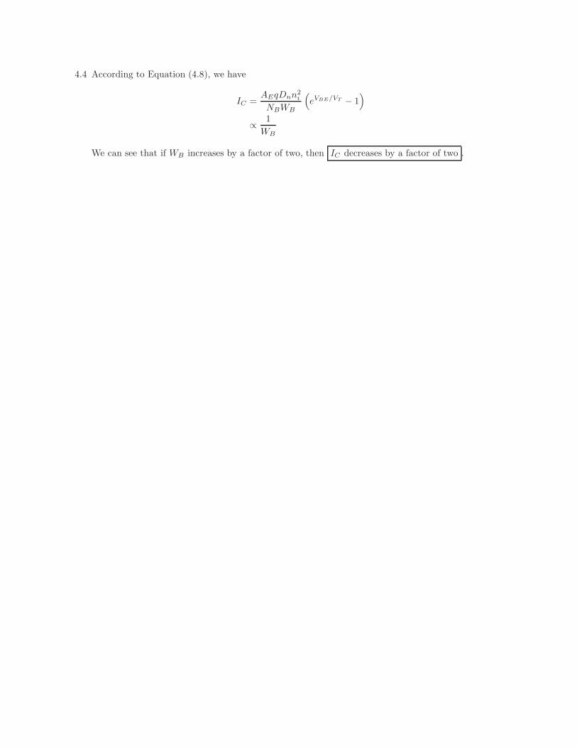
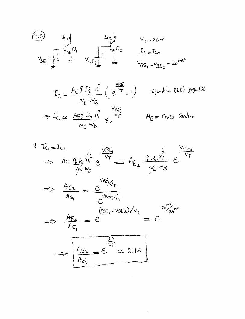
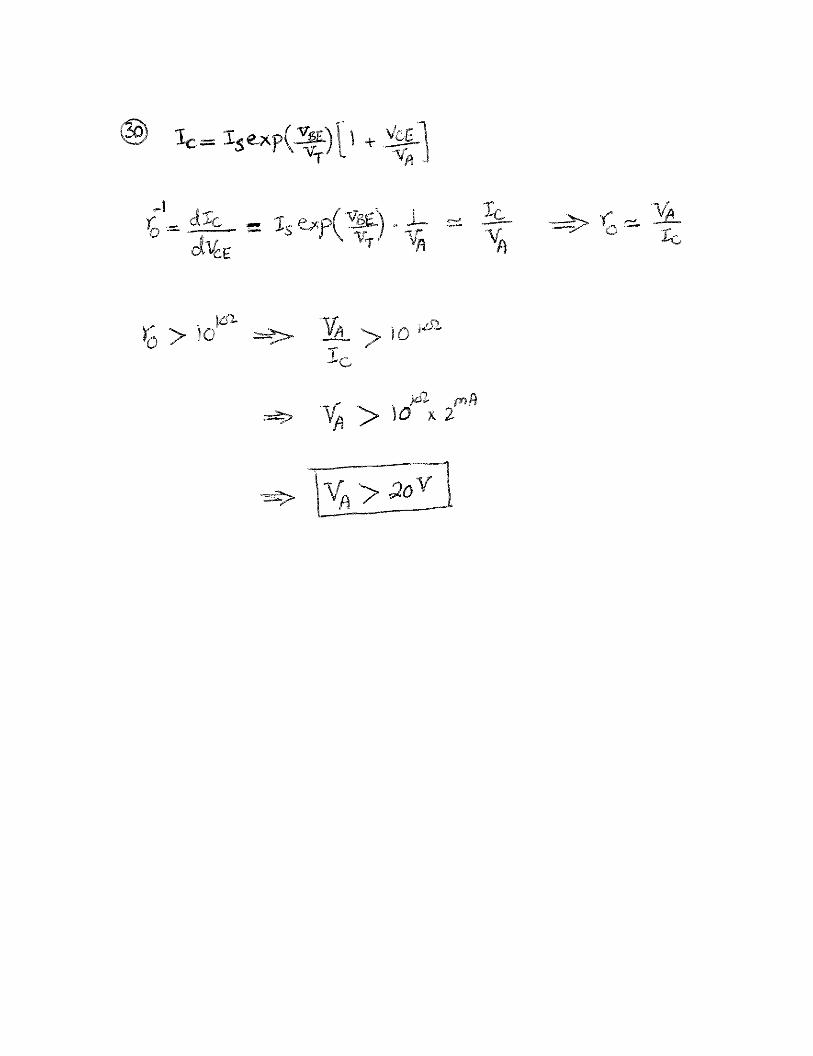
4.4 According to Equation (4.8), we have
IC =AEqDnn2
i
NBWB
(
eVBE/VT − 1)
∝1
WB
We can see that if WB increases by a factor of two, then IC decreases by a factor of two .
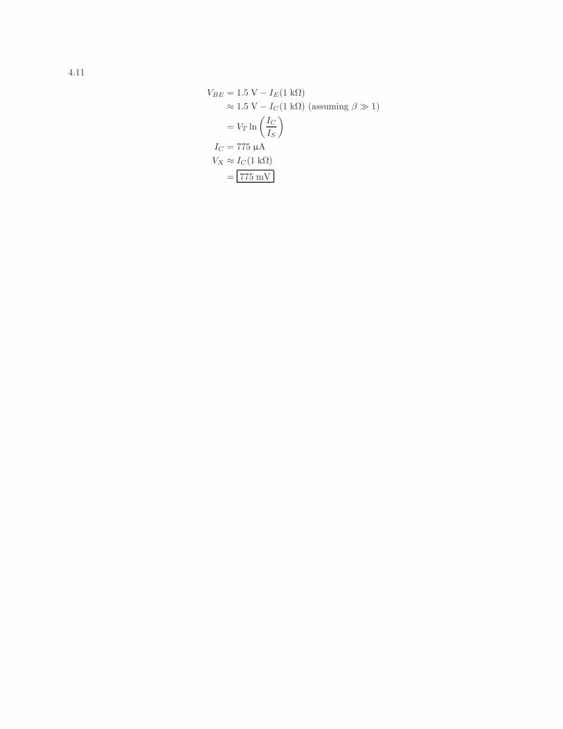
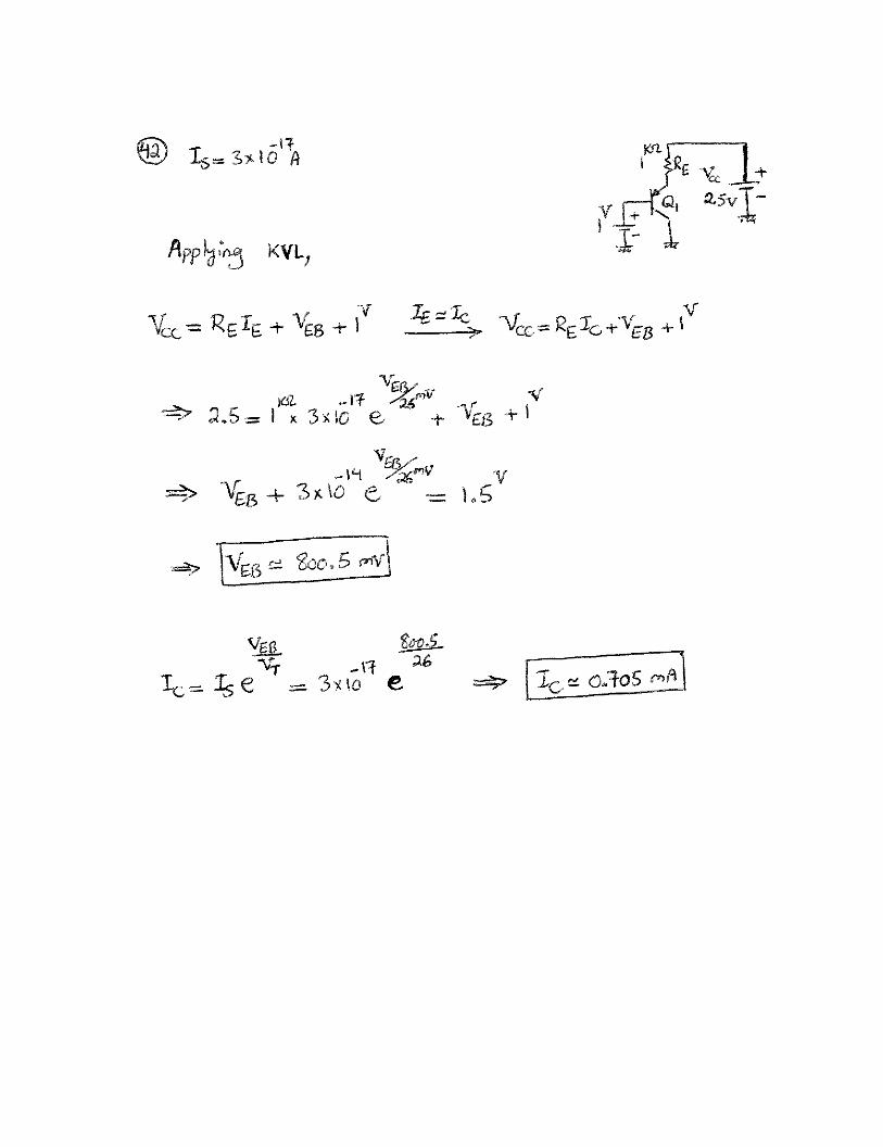
4.11
VBE = 1.5 V − IE(1 kΩ)
≈ 1.5 V − IC(1 kΩ) (assuming β ≫ 1)
= VT ln
(
IC
IS
)
IC = 775 µA
VX ≈ IC(1 kΩ)
= 775 mV
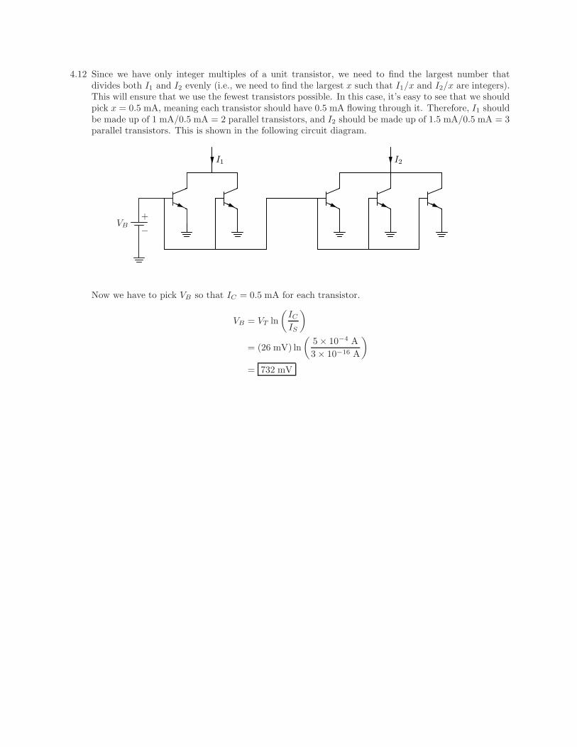
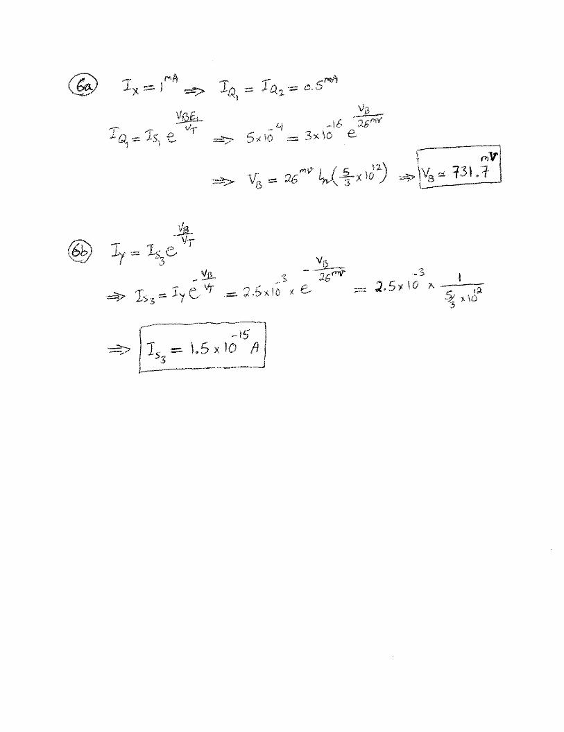
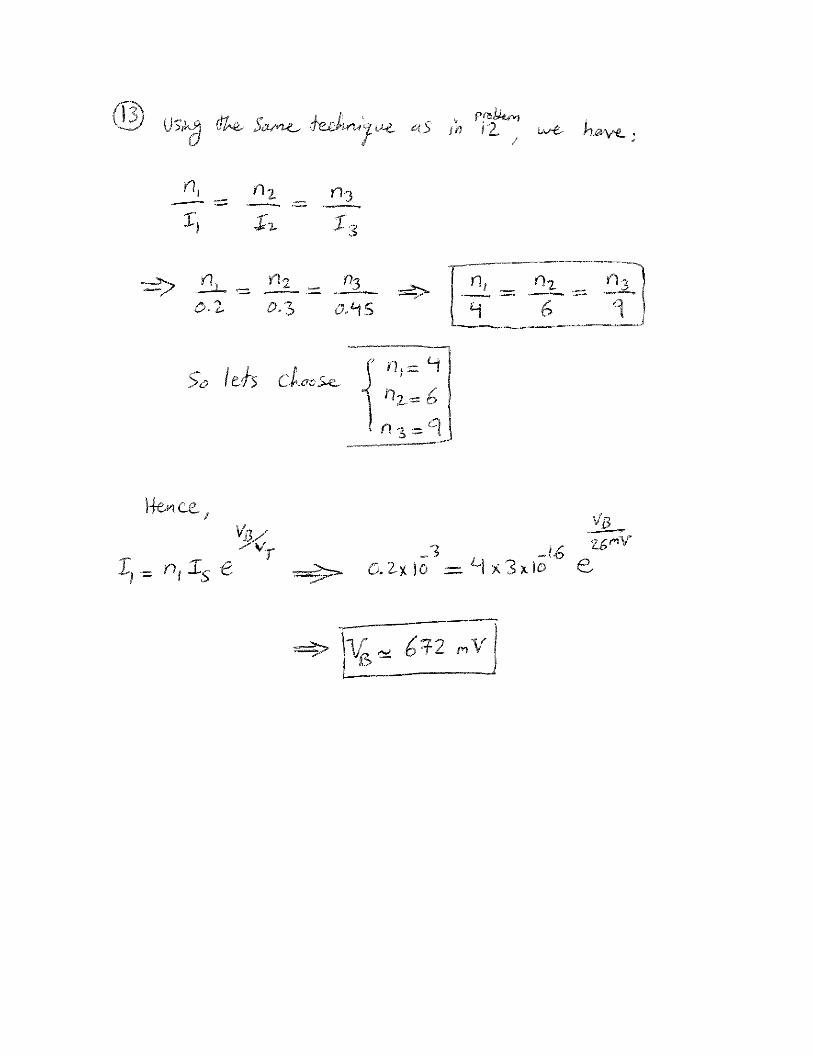
4.12 Since we have only integer multiples of a unit transistor, we need to find the largest number thatdivides both I1 and I2 evenly (i.e., we need to find the largest x such that I1/x and I2/x are integers).This will ensure that we use the fewest transistors possible. In this case, it’s easy to see that we shouldpick x = 0.5 mA, meaning each transistor should have 0.5 mA flowing through it. Therefore, I1 shouldbe made up of 1 mA/0.5 mA = 2 parallel transistors, and I2 should be made up of 1.5 mA/0.5 mA = 3parallel transistors. This is shown in the following circuit diagram.
VB−
+
I1 I2
Now we have to pick VB so that IC = 0.5 mA for each transistor.
VB = VT ln
(
IC
IS
)
= (26 mV) ln
(
5 × 10⁻⁴ A
3 × 10⁻¹⁶ A
)
= 732 mV
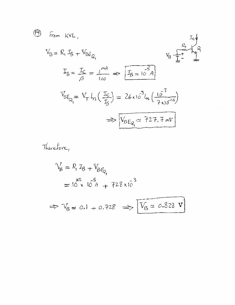
4.15
VB − VBE
R1
= IB
=IC
β
IC =β
R1
[VB − VT ln(IC/IS)]
IC = 786 µA
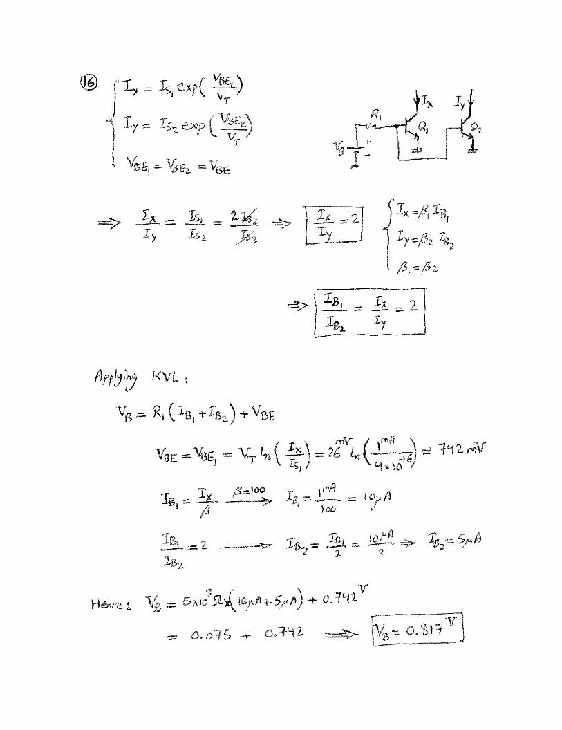
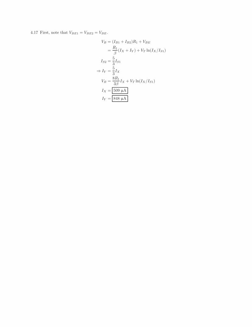
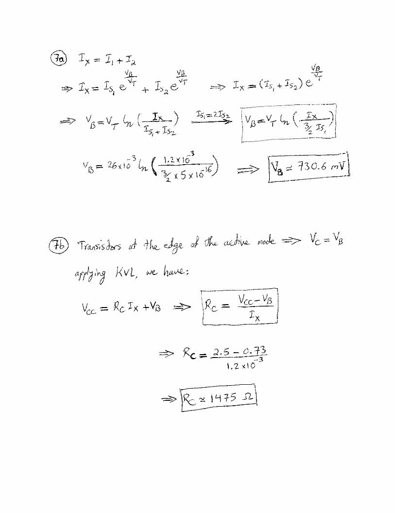
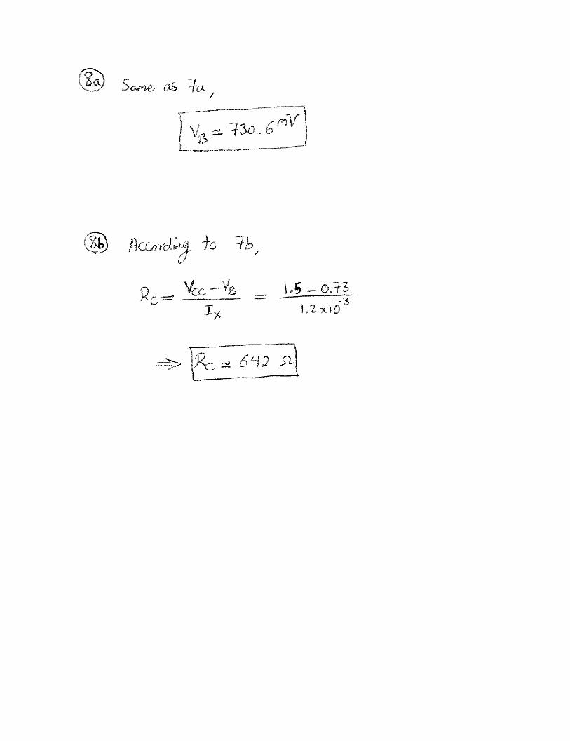
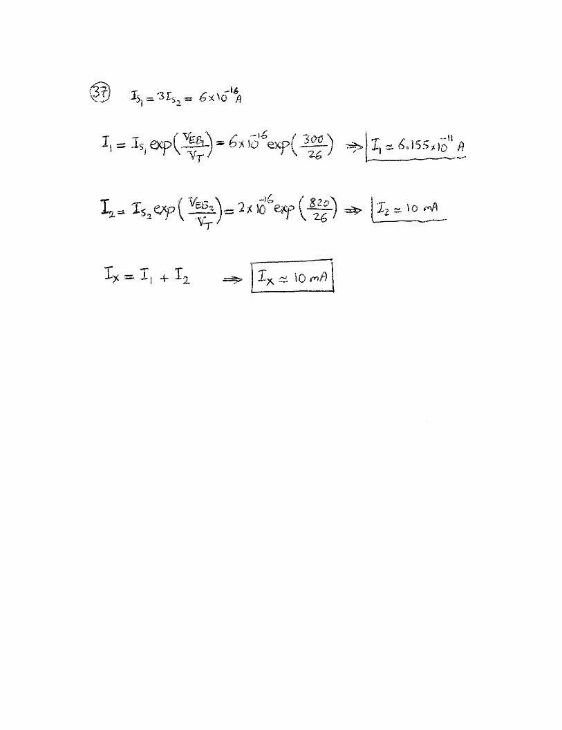
4.17 First, note that VBE1 = VBE2 = VBE .
VB = (IB1 + IB2)R1 + VBE
=R1
β(IX + IY ) + VT ln(IX/IS1)
IS2 =5
3IS1
⇒ IY =5
3IX
VB =8R1
3βIX + VT ln(IX/IS1)
IX = 509 µA
IY = 848 µA
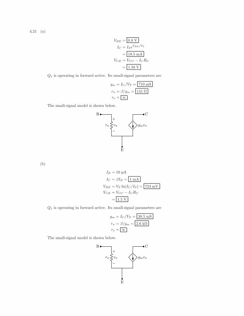
4.21 (a)
VBE = 0.8 V
IC = ISeVBE/VT
= 18.5 mA
VCE = VCC − ICRC
= 1.58 V
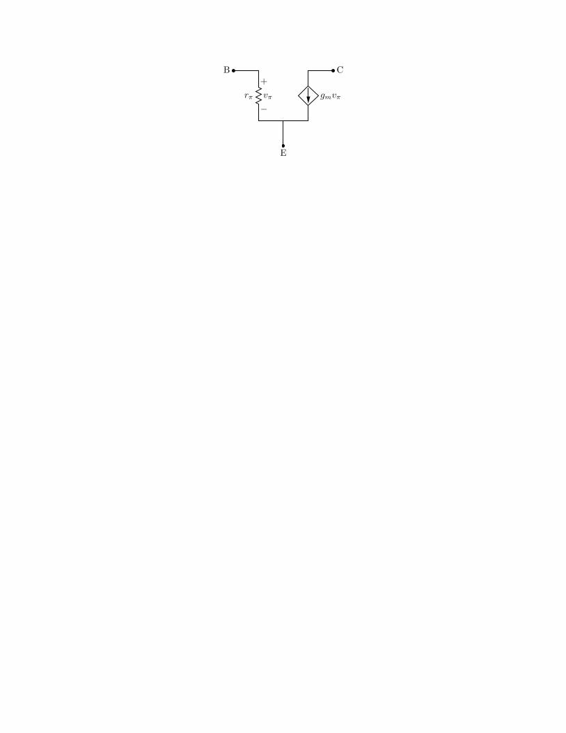
Q1 is operating in forward active. Its small-signal parameters are
gm = IC/VT = 710 mS
rπ = β/gm = 141 Ω
ro = ∞
The small-signal model is shown below.
B
rπ
+
vπ
−
E
gmvπ
C
(b)
IB = 10 µA
IC = βIB = 1 mA
VBE = VT ln(IC/IS) = 724 mV
VCE = VCC − ICRC
= 1.5 V
Q1 is operating in forward active. Its small-signal parameters are
gm = IC/VT = 38.5 mS
rπ = β/gm = 2.6 kΩ
ro = ∞
The small-signal model is shown below.
B
rπ
+
vπ
−
E
gmvπ
C
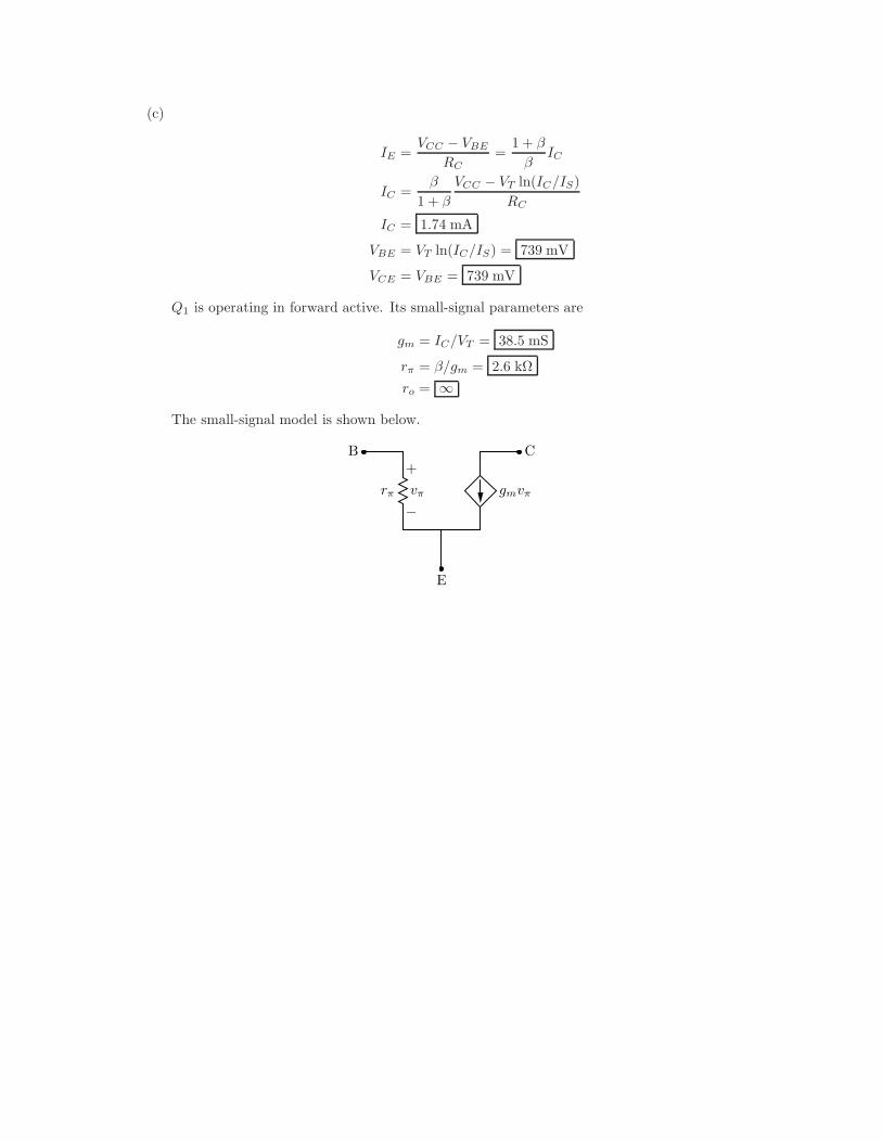
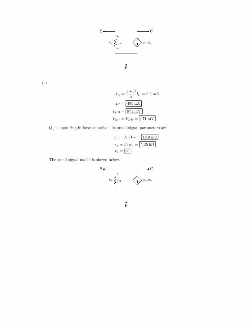
(c)
IE =VCC − VBE
RC=
1 + β
βIC
IC =β
1 + β
VCC − VT ln(IC/IS)
RC
IC = 1.74 mA
VBE = VT ln(IC/IS) = 739 mV
VCE = VBE = 739 mV
Q1 is operating in forward active. Its small-signal parameters are
gm = IC/VT = 38.5 mS
rπ = β/gm = 2.6 kΩ
ro = ∞
The small-signal model is shown below.
B
rπ
+
vπ
−
E
gmvπ
C
4.22 (a)
IB = 10 µA
IC = βIB = 1 mA
VBE = VT ln(IC/IS) = 739 mV
VCE = VCC − IE(1 kΩ)
= VCC −1 + β
β(1 kΩ)
= 0.99 V
Q1 is operating in forward active. Its small-signal parameters are
gm = IC/VT = 38.5 mS
rπ = β/gm = 2.6 kΩ
ro = ∞
The small-signal model is shown below.
B
rπ
+
vπ
−
E
gmvπ
C
(b)
IE =VCC − VBE
1 kΩ=
1 + β
βIC
IC =β
1 + β
VCC − VT ln(IC/IS)
1 kΩ
IC = 1.26 mA
VBE = VT ln(IC/IS) = 730 mV
VCE = VBE = 730 mV
Q1 is operating in forward active. Its small-signal parameters are
gm = IC/VT = 48.3 mS
rπ = β/gm = 2.07 kΩ
ro = ∞
The small-signal model is shown below.
B
rπ
+
vπ
−
E
gmvπ
C
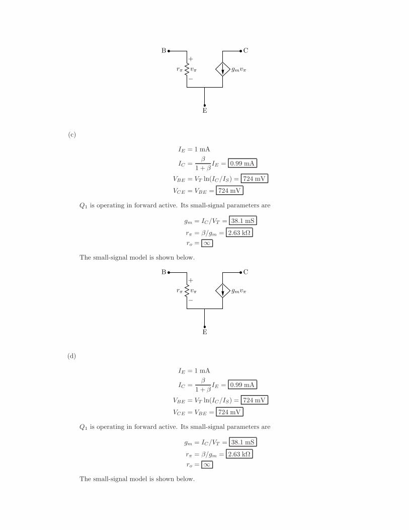
(c)
IE = 1 mA
IC =β
1 + βIE = 0.99 mA
VBE = VT ln(IC/IS) = 724 mV
VCE = VBE = 724 mV
Q1 is operating in forward active. Its small-signal parameters are
gm = IC/VT = 38.1 mS
rπ = β/gm = 2.63 kΩ
ro = ∞
The small-signal model is shown below.
B
rπ
+
vπ
−
E
gmvπ
C
(d)
IE = 1 mA
IC =β
1 + βIE = 0.99 mA
VBE = VT ln(IC/IS) = 724 mV
VCE = VBE = 724 mV
Q1 is operating in forward active. Its small-signal parameters are
gm = IC/VT = 38.1 mS
rπ = β/gm = 2.63 kΩ
ro = ∞
The small-signal model is shown below.
B
rπ
+
vπ
−
E
gmvπ
C
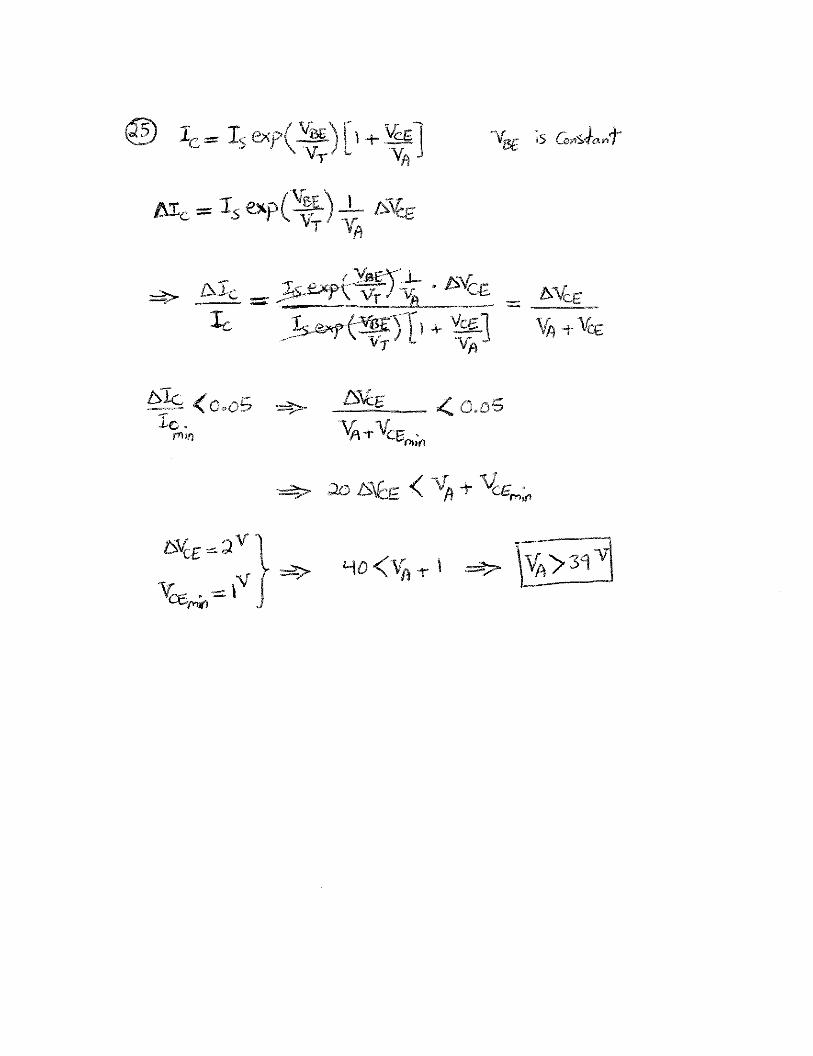
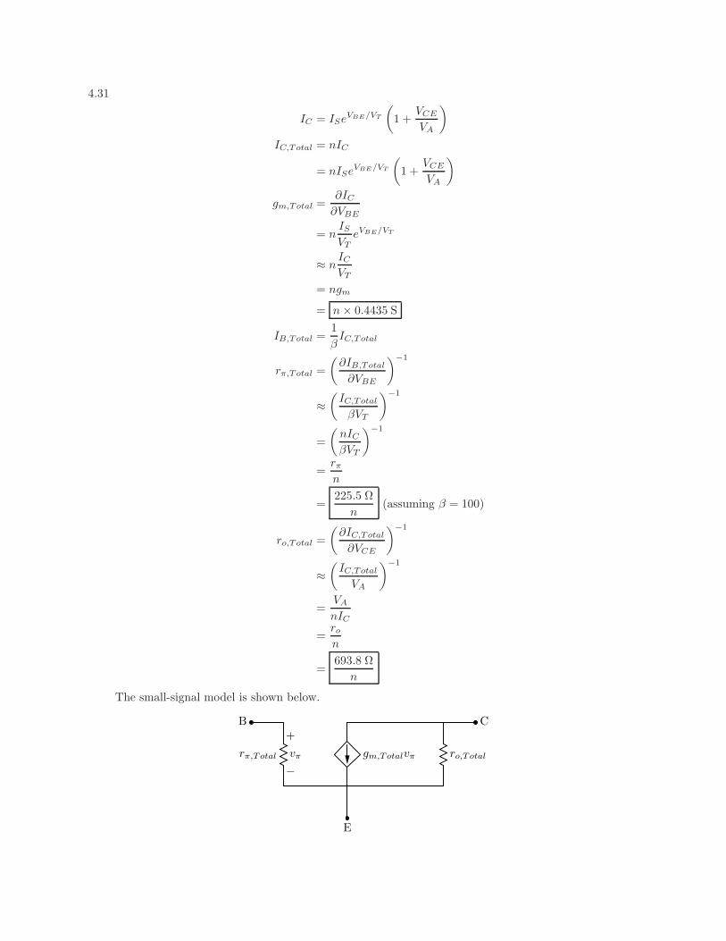
4.31
IC = ISeVBE/VT
(
1 +VCE
VA
)
IC,Total = nIC
= nISeVBE/VT
(
1 +VCE
VA
)
gm,Total =∂IC
∂VBE
= nIS
VTeVBE/VT
≈ nIC
VT
= ngm
= n × 0.4435 S
IB,Total =1
βIC,Total
rπ,Total =
(
∂IB,Total
∂VBE
)
−1
≈
(
IC,Total
βVT
)
−1
=
(
nIC
βVT
)
−1
=rπ
n
=225.5 Ω
n(assuming β = 100)
ro,Total =
(
∂IC,Total
∂VCE
)
−1
≈
(
IC,Total
VA
)
−1
=VA
nIC
=ro
n
=693.8 Ω
n
The small-signal model is shown below.
B
rπ,Total
+
vπ
−
E
gm,Totalvπ
C
ro,Total
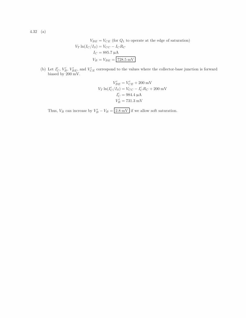
4.32 (a)
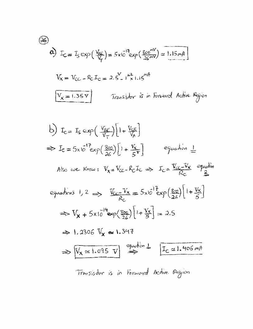
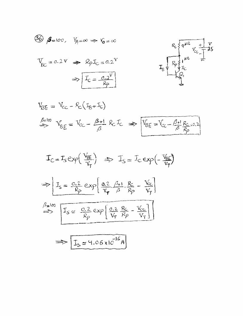
VBE = VCE (for Q1 to operate at the edge of saturation)
VT ln(IC/IS) = VCC − ICRC
IC = 885.7 µA
VB = VBE = 728.5 mV
(b) Let I ′C , V ′
B , V ′
BE , and V ′
CE correspond to the values where the collector-base junction is forwardbiased by 200 mV.
V ′
BE = V ′
CE + 200 mV
VT ln(I ′C/IS) = VCC − I ′CRC + 200 mV
I ′C = 984.4 µA
V ′
B = 731.3 mV
Thus, VB can increase by V ′
B − VB = 2.8 mV if we allow soft saturation.
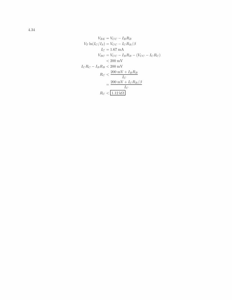
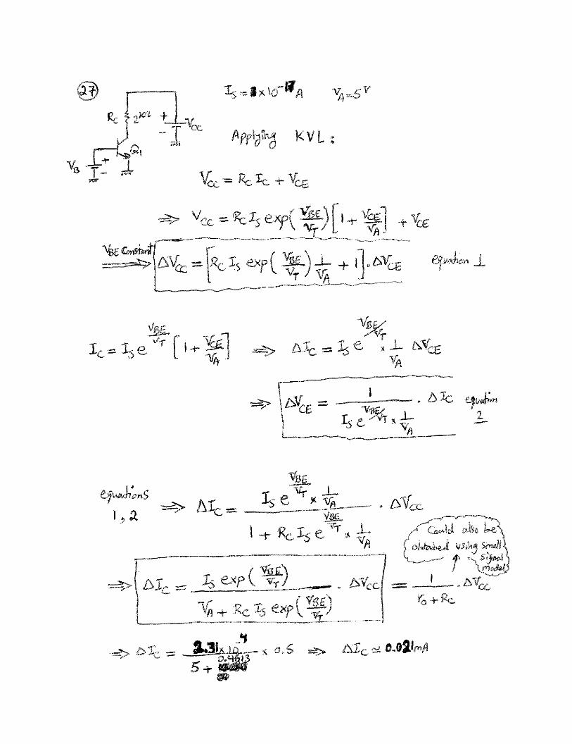
4.34
VBE = VCC − IBRB
VT ln(IC/IS) = VCC − ICRB/β
IC = 1.67 mA
VBC = VCC − IBRB − (VCC − ICRC)
< 200 mV
ICRC − IBRB < 200 mV
RC <200 mV + IBRB
IC
=200 mV + ICRB/β
IC
RC < 1.12 kΩ
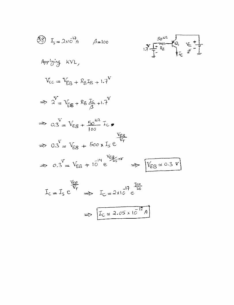
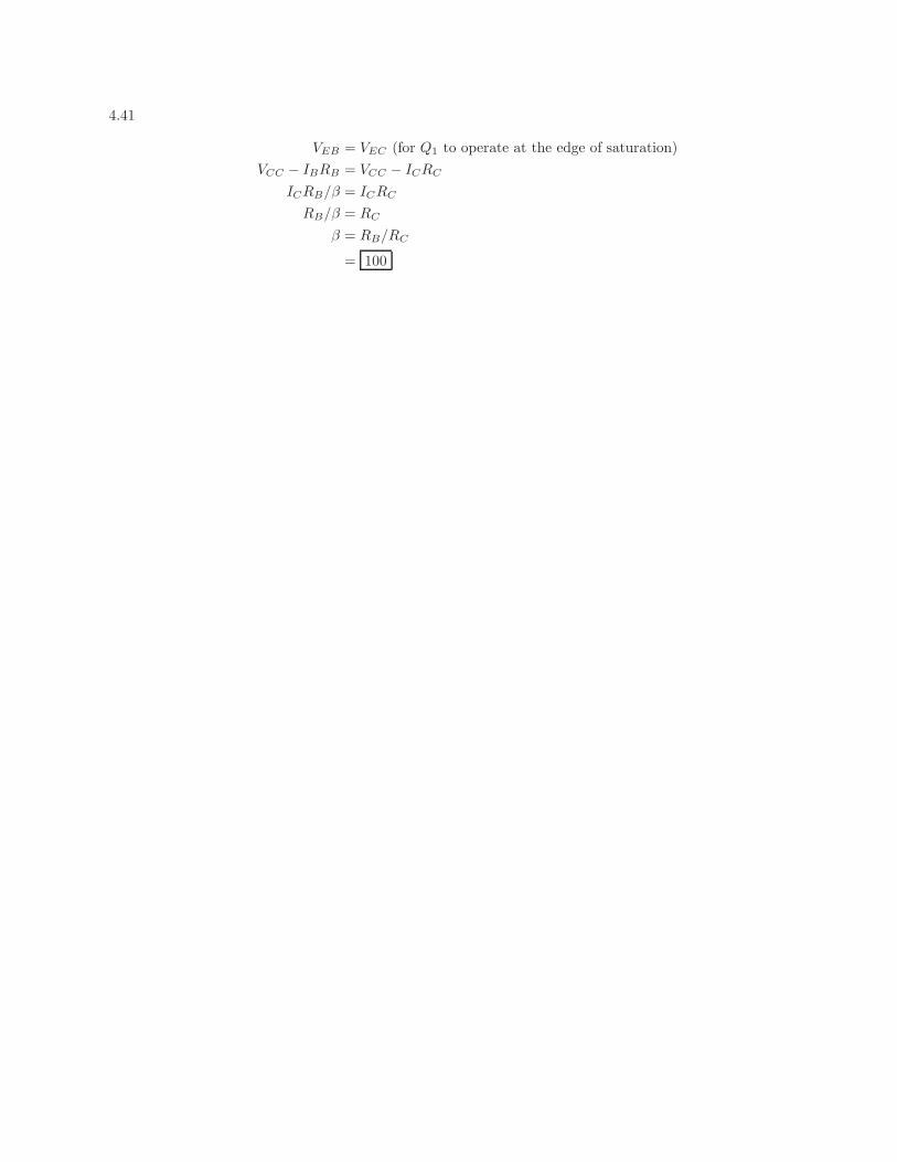
4.41
VEB = VEC (for Q1 to operate at the edge of saturation)
VCC − IBRB = VCC − ICRC
ICRB/β = ICRC
RB/β = RC
β = RB/RC
= 100
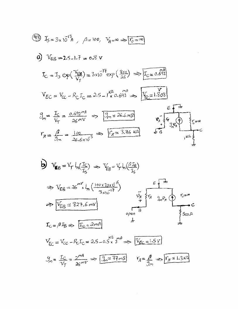
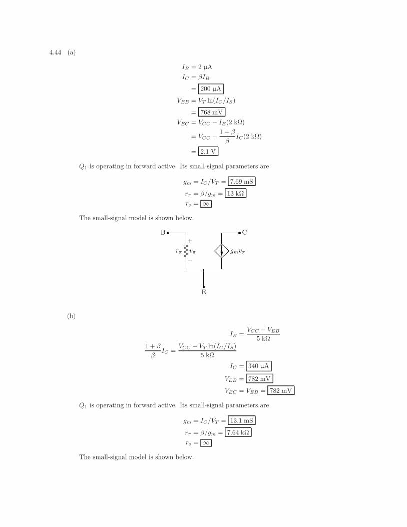
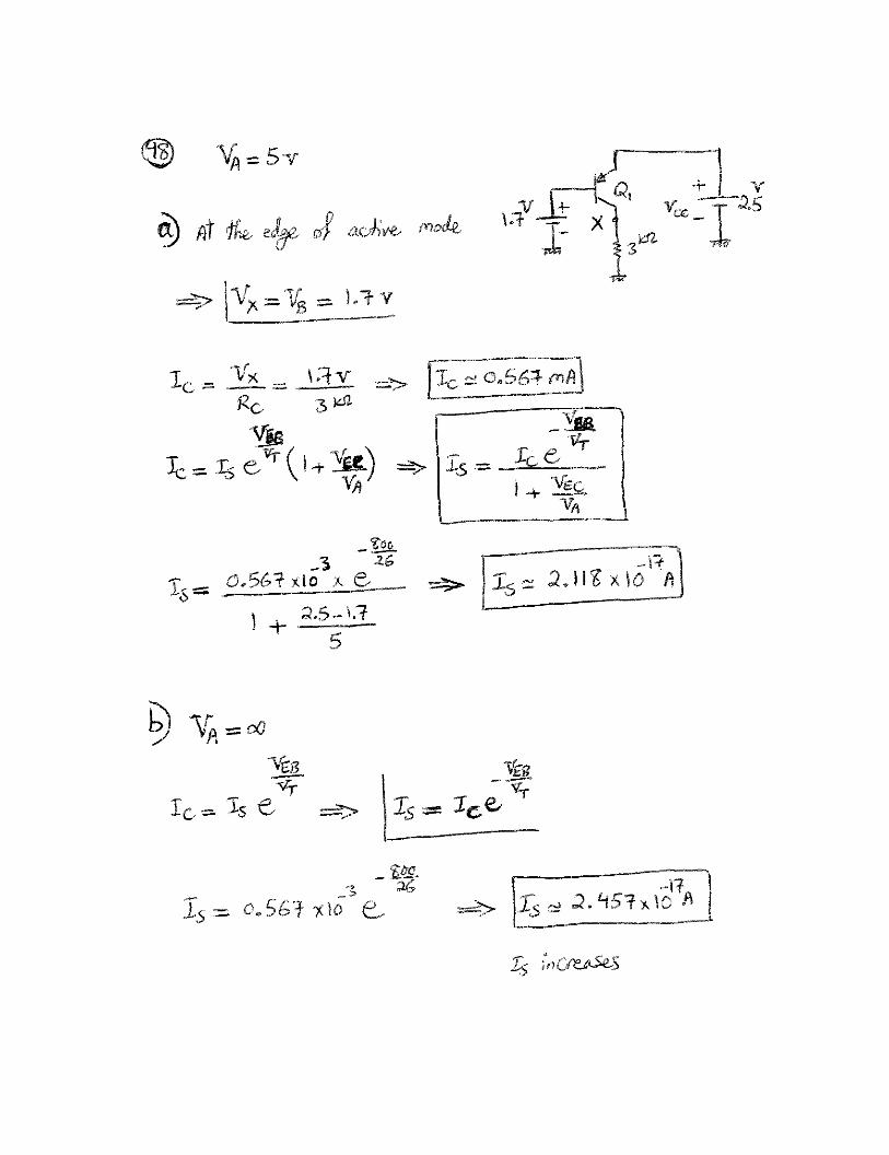
4.44 (a)
IB = 2 µA
IC = βIB
= 200 µA
VEB = VT ln(IC/IS)
= 768 mV
VEC = VCC − IE(2 kΩ)
= VCC −1 + β
βIC(2 kΩ)
= 2.1 V
Q1 is operating in forward active. Its small-signal parameters are
gm = IC/VT = 7.69 mS
rπ = β/gm = 13 kΩ
ro = ∞
The small-signal model is shown below.
B
rπ
+
vπ
−
E
gmvπ
C
(b)
IE =VCC − VEB
5 kΩ1 + β
βIC =
VCC − VT ln(IC/IS)
5 kΩ
IC = 340 µA
VEB = 782 mV
VEC = VEB = 782 mV
Q1 is operating in forward active. Its small-signal parameters are
gm = IC/VT = 13.1 mS
rπ = β/gm = 7.64 kΩ
ro = ∞
The small-signal model is shown below.
B
rπ
+
vπ
−
E
gmvπ
C
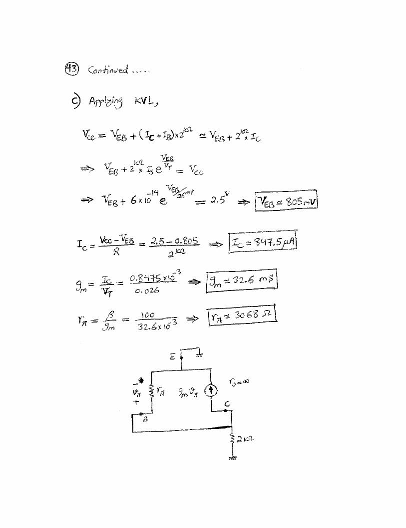
(c)
IE =1 + β
βIC = 0.5 mA
IC = 495 µA
VEB = 971 mV
VEC = VEB = 971 mV
Q1 is operating in forward active. Its small-signal parameters are
gm = IC/VT = 19.0 mS
rπ = β/gm = 5.25 kΩ
ro = ∞
The small-signal model is shown below.
B
rπ
+
vπ
−
E
gmvπ
C
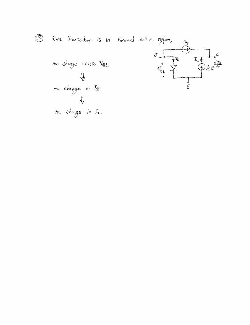
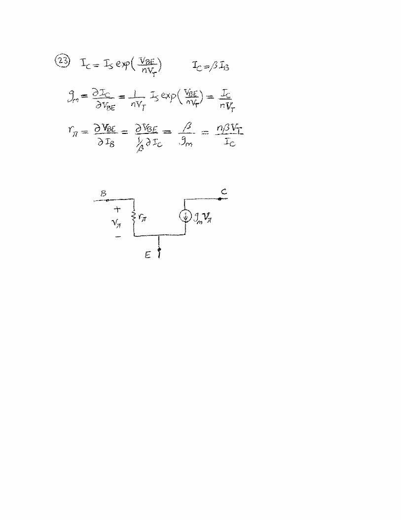
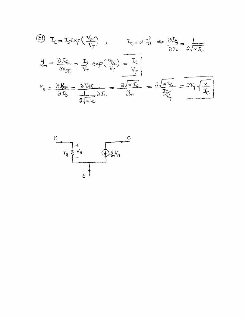
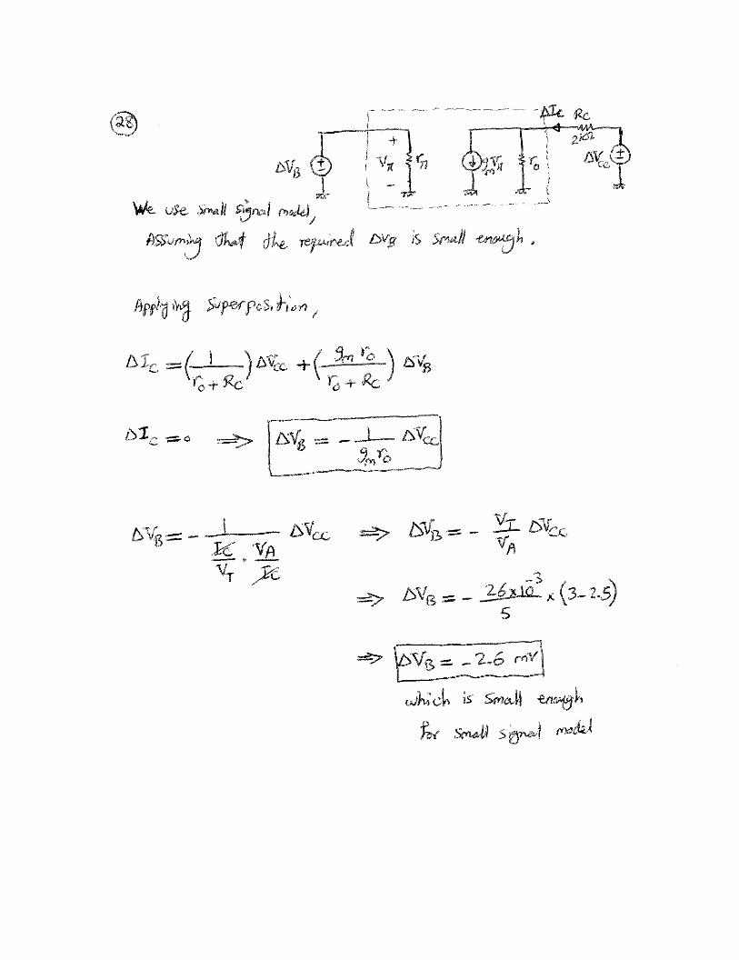
4.49 The direction of current flow in the large-signal model (Fig. 4.40) indicates the direction of positivecurrent flow when the transistor is properly biased.
The direction of current flow in the small-signal model (Fig. 4.43) indicates the direction of positivechange in current flow when the base-emitter voltage vbe increases. For example, when vbe increases,the current flowing into the collector increases, which is why ic is shown flowing into the collector inFig. 4.43. Similar reasoning can be applied to the direction of flow of ib and ie in Fig. 4.43.
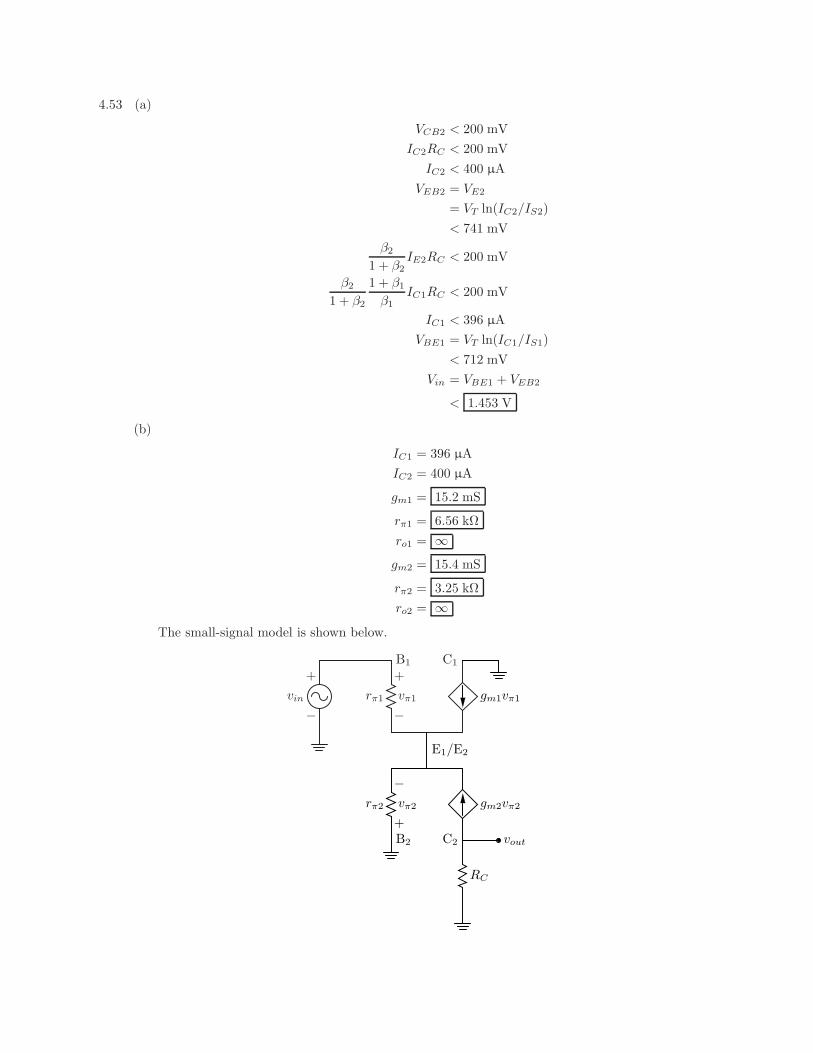
4.53 (a)
VCB2 < 200 mV
IC2RC < 200 mV
IC2 < 400 µA
VEB2 = VE2
= VT ln(IC2/IS2)
< 741 mV
β2
1 + β2
IE2RC < 200 mV
β2
1 + β2
1 + β1
β1
IC1RC < 200 mV
IC1 < 396 µA
VBE1 = VT ln(IC1/IS1)
< 712 mV
Vin = VBE1 + VEB2
< 1.453 V
(b)
IC1 = 396 µA
IC2 = 400 µA
gm1 = 15.2 mS
rπ1 = 6.56 kΩ
ro1 = ∞
gm2 = 15.4 mS
rπ2 = 3.25 kΩ
ro2 = ∞
The small-signal model is shown below.
−
vin
+B1
rπ1
+
vπ1
−
C1
gm1vπ1
E1/E2
rπ2
−
vπ2
+B2
gm2vπ2
C2 vout
RC
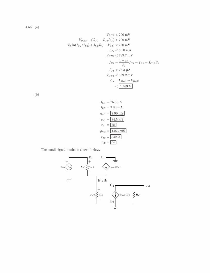
4.55 (a)
VBC2 < 200 mV
VBE2 − (VCC − IC2RC) < 200 mV
VT ln(IC2/IS2) + IC2RC − VCC < 200 mV
IC2 < 3.80 mA
VBE2 < 799.7 mV
IE1 =1 + β1
β1
IC1 = IB2 = IC2/β2
IC1 < 75.3 µA
VBE1 < 669.2 mV
Vin = VBE1 + VBE2
< 1.469 V
(b)
IC1 = 75.3 µA
IC2 = 3.80 mA
gm1 = 2.90 mS
rπ1 = 34.5 kΩ
ro1 = ∞
gm2 = 146.2 mS
rπ2 = 342 Ω
ro2 = ∞
The small-signal model is shown below.
−
vin
+B1
rπ1
+
vπ1
−
C1
gm1vπ1
E1/B2
rπ2
+
vπ2
−
C2
gm2vπ2
E2
vout
RC


![94 زییاپ کینورتکلا لوصا 2 هرامش نیرمتsharif.edu/~kavehvash/HW2.pdf · · 2016-02-17BR Wiley/Razavi/Fundamentals of Microelectronics [Razavi.cls v. 2006]](https://img.pdfslide.tips/doc/110x75/5aefd7f37f8b9a572b8eadda/94-2-kavehvashhw2pdf2016-02-17br.jpg)


![Arbaeen'e Razavi [Urdu]](https://img.pdfslide.tips/doc/110x75/577cdeb51a28ab9e78afa861/arbaeene-razavi-urdu.jpg)