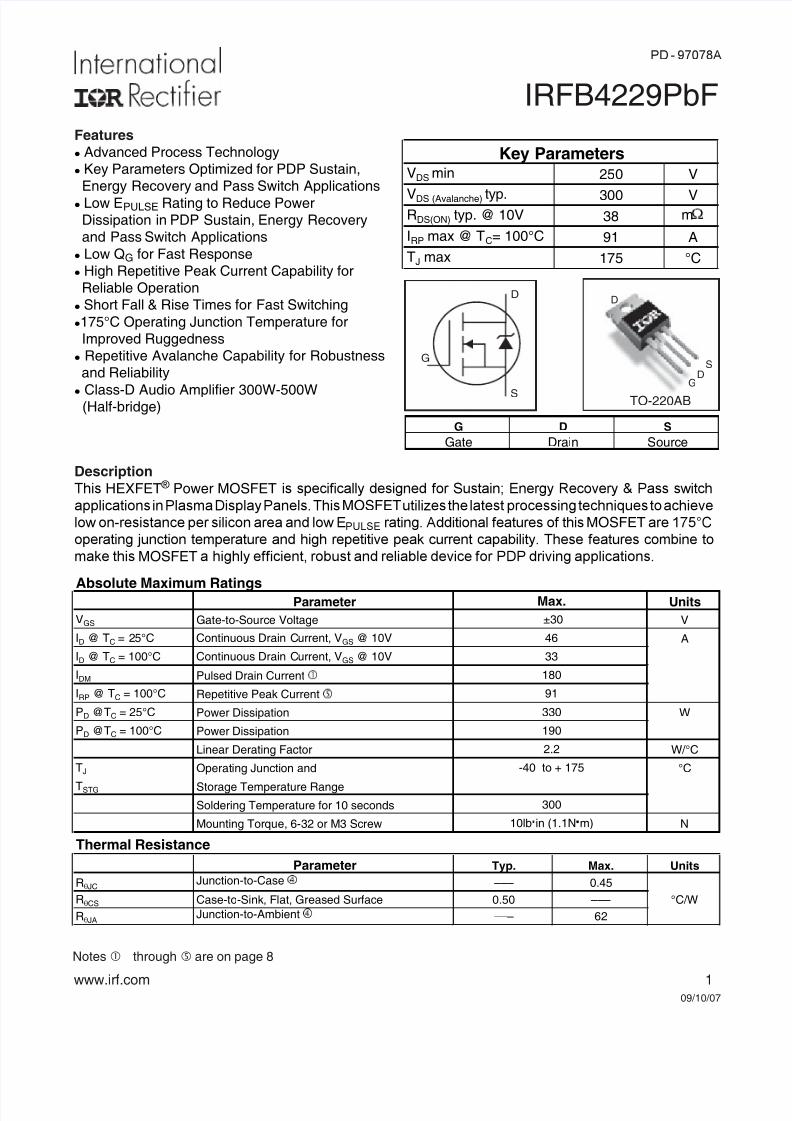
www.irf.com 1 09/10/07 IRFB4229PbF Notesthrough are on page 8 Description HEXFET ®Power MOSFETMOSFETMOSFETMOSFETS D G TO-220AB D S D G G D S Gate Drain Source V DS min 250 V V DS (Avalanche) typ. 300 V R DS(ON) typ. @ 10V 38 m I RP max @ T C = 100°C 91 A T J max 175 °C Key Parameters Absolute Maximum Ratings Parameter Units V GS Gate-to-Source Voltage V I D @ T C = 25°C Continuous Drain Current, V GS @ 10V A I D @ T C = 100°C Continuous Drain Current, V GS @ 10V I DM Pulsed Drain Current I RP @ T C = 100°C Repetitive Peak Current P D @T C = 25°C Power Dissipation W P D @T C = 100°C Power Dissipation Linear Derating Factor W/°C T J Operating Junction and °C T STG Storage Temperature Range Soldering Temperature for 10 seconds Mounting Torque, 6-32 or M3 Screw N Thermal Resistance Parameter Typ. Max. Units R θJC Junction-to-Case ––– 0.45 R θCS Case-to-Sink, Flat, Greased Surface 0.50 ––– °C/W R θJA Junction-to-Ambient ––– 62 91 300 -40 to + 175 10lb in (1.1N m) 330 190 2.2 Max. 33 180 46 ±30 Features Advanced Process Technology Key Parameters Optimized for PDP Sustain, Energy Recovery and Pass Switch Applications Low E PULSE Rating to Reduce Power Dissipation in PDP Sustain, Energy Recovery and Pass Switch Applications Low Q G for Fast Response High Repetitive Peak Current Capability for Reliable Operation Short Fall & Rise Times for Fast Switching 175°C Operating Junction Temperature for Improved Ruggedness Repetitive Avalanche Capability for Robustness and Reliability Class-D Audio Amplifier 300W-500W (Half-bridge)