Embed Size (px)
Citation preview

Chapter 4 - 1
ISSUES TO ADDRESS...
• What types of defects arise in solids?
• Can the number and type of defects be variedand controlled?
• How do defects affect material properties?
• Are defects undesirable?
Chapter 4:Imperfections in Solids
• What are the solidification mechanisms?

Chapter 4 - 2
• Solidification- result of casting of molten material– 2 steps
• Nuclei form • Nuclei grow to form crystals – grain structure
• Start with a molten material – all liquid
Imperfections in Solids
• Crystals grow until they meet each otherAdapted from Fig. 4.14(b), Callister & Rethwisch 8e.
grain structurecrystals growingnucleiliquid
Chapter 4 - 3
Polycrystalline Materials
Grain Boundaries• regions between crystals• transition from lattice of
one region to that of the other
• slightly disordered• low density in grain
boundaries– high mobility– high diffusivity– high chemical reactivity
Adapted from Fig. 4.7, Callister & Rethwisch 8e.
Chapter 4 - 4
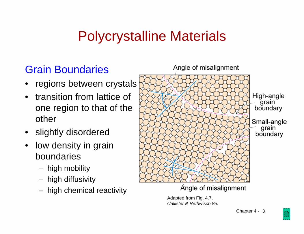
Solidification
Columnar in area with less undercooling
Shell of equiaxed grains due to rapid cooling (greater T) near wall
Grain Refiner - added to make smaller, more uniform, equiaxed grains.
heat flow
Grains can be - equiaxed (roughly same size in all directions)- columnar (elongated grains)
Adapted from Fig. 5.17, Callister & Rethwisch 3e.
~ 8 cm

Chapter 4 - 5
Imperfections in Solids
There is no such thing as a perfect crystal. • What are these imperfections? • Why are they important?
Many of the important properties of materials are due to the presence of imperfections.

Chapter 4 - 6
• Vacancy atoms• Interstitial atoms• Substitutional atoms
Point defects
Types of Imperfections
• Dislocations Line defects
• Grain Boundaries Area defects

Chapter 4 - 7
• Vacancies:-vacant atomic sites in a structure.
• Self-Interstitials:-"extra" atoms positioned between atomic sites.
Point Defects in Metals
Vacancydistortion of planes
self-interstitial
distortion of planes

Chapter 4 -
8
Boltzmann's constant(1.38 x 10⁻²³ J/atom-K) (8.62 x 10⁻⁵ eV/atom-K)
NvN
expQvkT
No. of defects
No. of potential defect sites
Activation energy
Temperature
Each lattice site is a potential vacancy site
• Equilibrium concentration varies with temperature!
Equilibrium Concentration:Point Defects

Chapter 4 - 9
• We can get Qv froman experiment.
NvN
= expQvkT
Measuring Activation Energy
• Measure this...
Nv
N
T
exponential dependence!
defect concentration
• Replot it...
1/T
NNv
ln-Qv /k
slope

Chapter 4 - 10
• Find the equil. # of vacancies in 1 m3 of Cu at 1000C.• Given:
ACu = 63.5 g/mol = 8.4 g/cm3
Qv = 0.9 eV/atom NA = 6.02 x 10²³ atoms/mol
Estimating Vacancy Concentration
For 1 m3 , N =N
AA
Cu
x x 1 m3= 8.0 x 1028 sites
= 2.7 x 10⁻⁴
8.62 x 10⁻⁵ eV/atom-K
0.9 eV/atom
1273 K
NvN
expQvkT
• Answer:Nv = (2.7 x 10⁻⁴)(8.0 x 1028) sites = 2.2 x 1025 vacancies

Chapter 4 - 11
• Low energy electronmicroscope view ofa (110) surface of NiAl.
• Increasing temperature causes surface island ofatoms to grow.
• Why? The equil. vacancyconc. increases via atommotion from the crystalto the surface, where they join the island.
Reprinted with permission from Nature (K.F. McCarty, J.A. Nobel, and N.C. Bartelt, "Vacancies inSolids and the Stability of Surface Morphology",Nature, Vol. 412, pp. 622-625 (2001). Image is5.75 m by 5.75 m.) Copyright (2001) Macmillan Publishers, Ltd.
Observing Equilibrium Vacancy Conc.
Island grows/shrinks to maintain equil. vancancy conc. in the bulk.
Click once on image to start animation

Chapter 4 - 12
Two outcomes if impurity (B) added to host (A):• Solid solution of B in A (i.e., random dist. of point defects)
• Solid solution of B in A plus particles of a newphase (usually for a larger amount of B)
OR
Substitutional solid soln.(e.g., Cu in Ni)
Interstitial solid soln.(e.g., C in Fe)
Second phase particle-- different composition-- often different structure.
Imperfections in Metals (i)

Chapter 4 - 13
Imperfections in Metals (ii)
Conditions for substitutional solid solution (S.S.)• W. Hume – Rothery rule
– 1. r (atomic radius) < 15%– 2. Proximity in periodic table
• i.e., similar electronegativities
– 3. Same crystal structure for pure metals– 4. Valency
• All else being equal, a metal will have a greater tendency to dissolve a metal of higher valency than one of lower valency

Chapter 4 - 14
Imperfections in Metals (iii)Application of Hume–Rothery rules – Solid
Solutions
1. Would you predictmore Al or Ag to dissolve in Zn?
2. More Zn or Al in Cu?
Table on p. 118, Callister & Rethwisch 8e.
Element Atomic Crystal Electro- ValenceRadius Structure nega-(nm) tivity
Cu 0.1278 FCC 1.9 +2C 0.071H 0.046O 0.060Ag 0.1445 FCC 1.9 +1Al 0.1431 FCC 1.5 +3Co 0.1253 HCP 1.8 +2Cr 0.1249 BCC 1.6 +3Fe 0.1241 BCC 1.8 +2Ni 0.1246 FCC 1.8 +2Pd 0.1376 FCC 2.2 +2Zn 0.1332 HCP 1.6 +2
Chapter 4 - 15
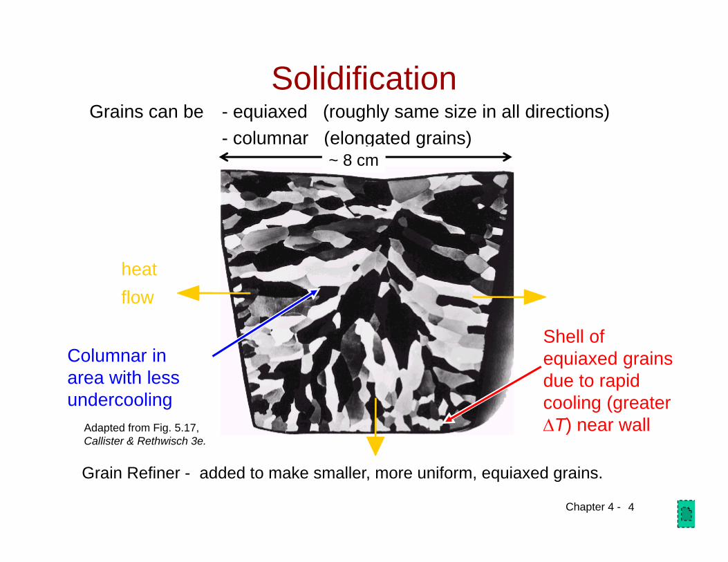
Impurities in Solids• Specification of composition
– weight percent 100x 21
11 mm
mC
m1 = mass of component 1
100x 21
1'1
mm
m
nnnC
nm1 = number of moles of component 1
– atom percent

Chapter 4 - 16
• are line defects,• slip between crystal planes result when dislocations move,• produce permanent (plastic) deformation.
Dislocations:
Schematic of Zinc (HCP):• before deformation • after tensile elongation
slip steps
Line Defects
Chapter 4 - 17
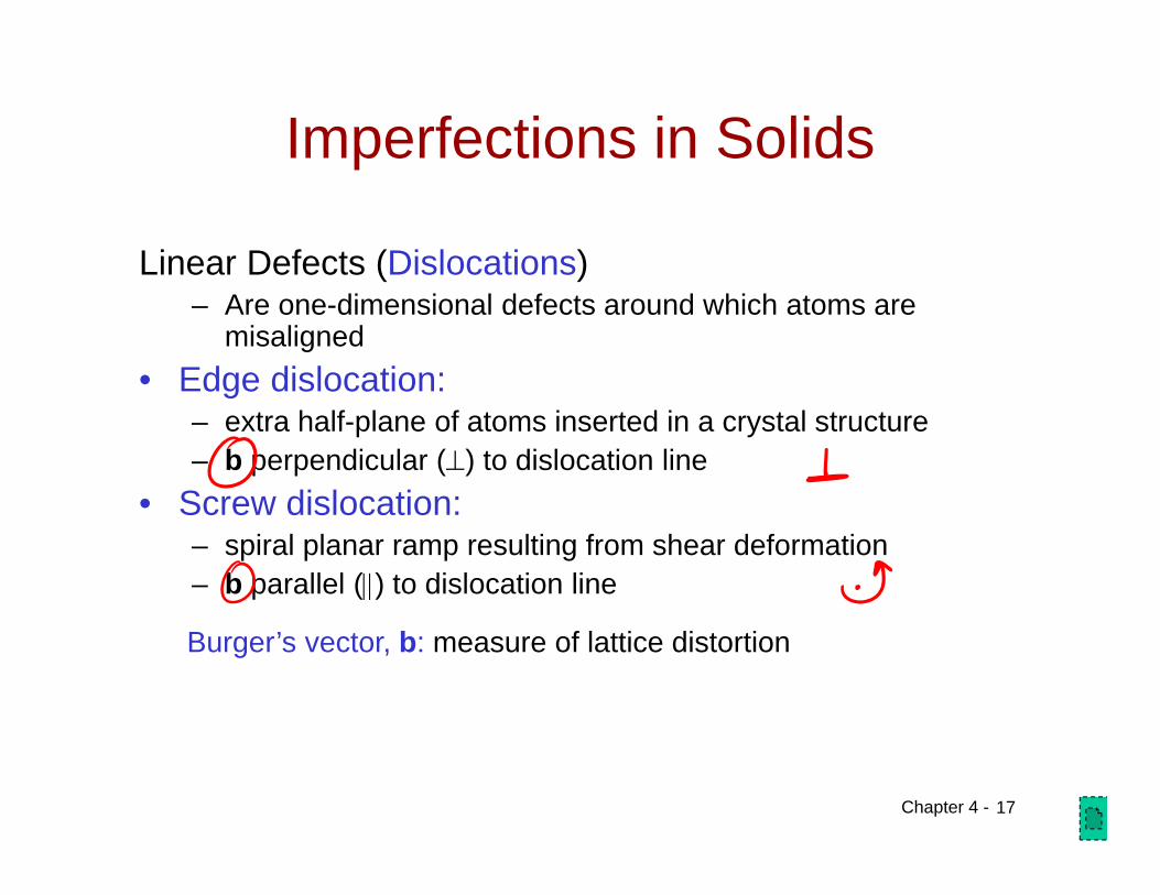
Imperfections in Solids
Linear Defects (Dislocations)– Are one-dimensional defects around which atoms are
misaligned• Edge dislocation:
– extra half-plane of atoms inserted in a crystal structure– b perpendicular () to dislocation line
• Screw dislocation:– spiral planar ramp resulting from shear deformation– b parallel () to dislocation line
Burger’s vector, b: measure of lattice distortion

Chapter 4 - 18
Imperfections in Solids
Fig. 4.3, Callister & Rethwisch 8e.
Edge Dislocation

Chapter 4 - 19
• Dislocation motion requires the successive bumpingof a half plane of atoms (from left to right here).
• Bonds across the slipping planes are broken andremade in succession.
Atomic view of edgedislocation motion fromleft to right as a crystalis sheared.
(Courtesy P.M. Anderson)
Motion of Edge Dislocation
Click once on image to start animation

Chapter 4 - 20
Imperfections in Solids
Screw Dislocation
Adapted from Fig. 4.4, Callister & Rethwisch 8e.
Burgers vector b
Dislocationline
b
(a)(b)
Screw Dislocation

Chapter 4 -
VMSE: Screw Dislocation• In VMSE:
– a region of crystal containing a dislocation can be rotated in 3D– dislocation motion may be animated
21Front View Top View
VMSE Screen Shots
Chapter 4 - 22
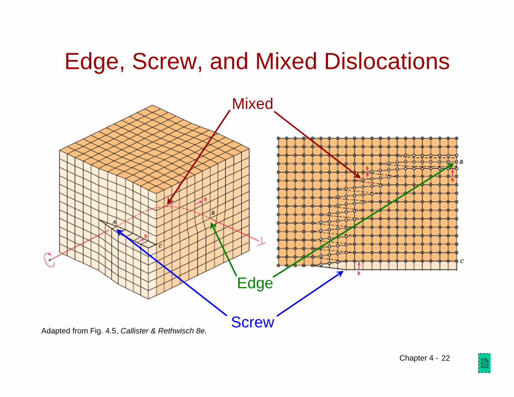
Edge, Screw, and Mixed Dislocations
Adapted from Fig. 4.5, Callister & Rethwisch 8e.
Edge
Screw
Mixed

Chapter 4 - 23
Imperfections in Solids
Dislocations are visible in electron micrographs
Fig. 4.6, Callister & Rethwisch 8e.

Chapter 4 - 24
Dislocations & Crystal Structures• Structure: close-packed
planes & directionsare preferred.
view onto twoclose-packedplanes.
close-packed plane (bottom) close-packed plane (top)close-packed directions
• Comparison among crystal structures:FCC: many close-packed planes/directions;HCP: only one plane, 3 directions;BCC: none
• Specimens that were tensiletested.
Mg (HCP)
Al (FCC)tensile direction

Chapter 4 - 25
Planar Defects in Solids
• One case is a twin boundary (plane)– Essentially a reflection of atom positions across the twin
plane.
• Stacking faults– For FCC metals an error in ABCABC packing sequence– Ex: ABCABABC
Adapted from Fig. 4.9, Callister & Rethwisch 8e.

Chapter 4 - 26
Catalysts and Surface Defects• A catalyst increases the
rate of a chemical reaction without being consumed
• Active sites on catalysts are normally surface defects
Fig. 4.10, Callister & Rethwisch 8e.
Fig. 4.11, Callister & Rethwisch 8e.
Single crystals of (Ce0.5Zr0.5)O2used in an automotive catalytic converter

Chapter 4 - 27
Microscopic Examination
• Crystallites (grains) and grain boundaries. Vary considerably in size. Can be quite large.– ex: Large single crystal of quartz or diamond or Si– ex: Aluminum light post or garbage can - see the
individual grains• Crystallites (grains) can be quite small (mm
or less) – necessary to observe with a microscope.

Chapter 4 - 28
• Useful up to 2000X magnification.• Polishing removes surface features (e.g., scratches)• Etching changes reflectance, depending on crystal
orientation.
Micrograph ofbrass (a Cu-Zn alloy)
0.75mm
Optical Microscopy
Adapted from Fig. 4.13(b) and (c), Callister & Rethwisch 8e. (Fig. 4.13(c) is courtesyof J.E. Burke, General Electric Co.)
crystallographic planes

Chapter 4 - 29
Grain boundaries...• are imperfections,• are more susceptible
to etching,• may be revealed as
dark lines,• change in crystal
orientation across boundary. Adapted from Fig. 4.14(a)
and (b), Callister & Rethwisch 8e.(Fig. 4.14(b) is courtesyof L.C. Smith and C. Brady, the National Bureau of Standards, Washington, DC [now the National Institute of Standards and Technology, Gaithersburg, MD].)
Optical Microscopy
ASTM grain size number
N = 2n-1
number of grains/in2
at 100x magnification
Fe-Cr alloy(b)
grain boundarysurface groove
polished surface
(a)

Chapter 4 - 30
Optical Microscopy
• Polarized light – metallographic scopes often use polarized
light to increase contrast– Also used for transparent samples such as
polymers

Chapter 4 - 31
MicroscopyOptical resolution ca. 10-7 m = 0.1 m = 100 nmFor higher resolution need higher frequency
– X-Rays? Difficult to focus.– Electrons
• wavelengths ca. 3 pm (0.003 nm) – (Magnification - 1,000,000X)
• Atomic resolution possible• Electron beam focused by magnetic lenses.

Chapter 4 - 32
• Atoms can be arranged and imaged!
Carbon monoxide molecules arranged on a platinum (111)
surface.
Photos produced from the work of C.P. Lutz, Zeppenfeld, and D.M. Eigler. Reprinted with permission from International Business Machines Corporation, copyright 1995.
Iron atoms arranged on a copper (111)
surface. These Kanji characters represent
the word “atom”.
Scanning Tunneling Microscopy(STM)

Chapter 4 - 33
• Point, Line, and Area defects exist in solids.
• The number and type of defects can be variedand controlled (e.g., T controls vacancy conc.)
• Defects affect material properties (e.g., grainboundaries control crystal slip).
• Defects may be desirable or undesirable(e.g., dislocations may be good or bad, dependingon whether plastic deformation is desirable or not.)
Summary

Chapter 4 - 34