Embed Size (px)
Citation preview
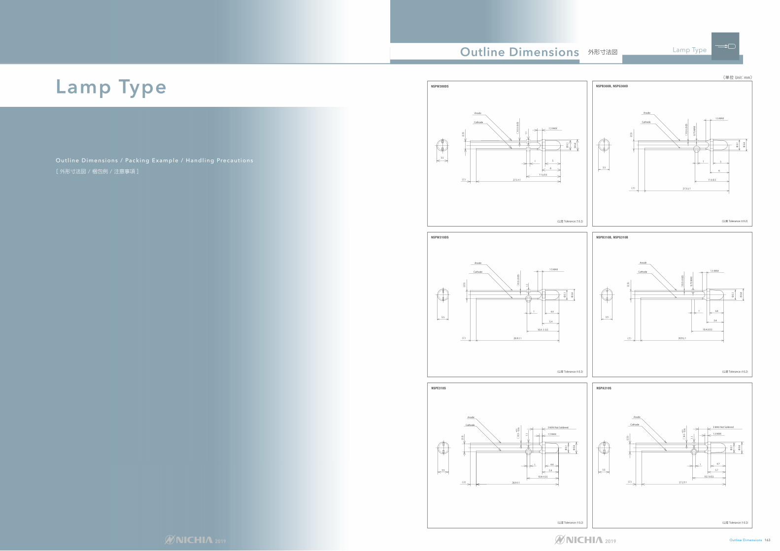
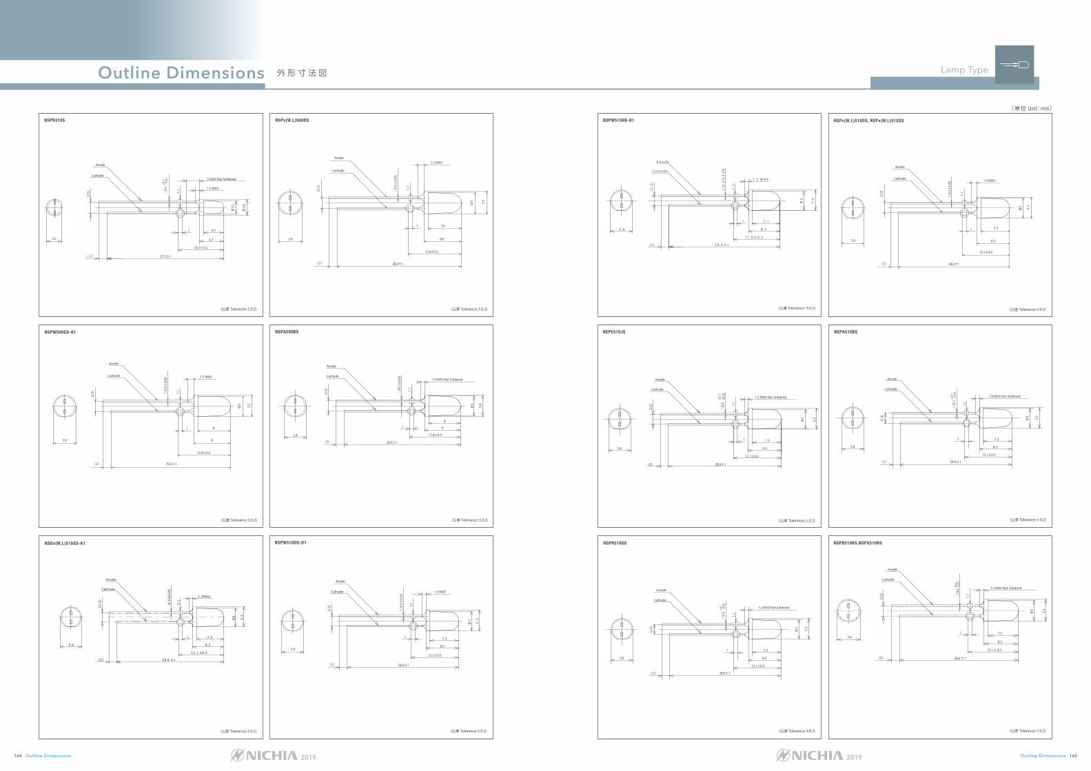
Lamp TypeOutline Dimensions 外形寸法図
Lamp Type
Out l ine Dimens ions / Pack ing Example / Handl ing Precaut ions
[ 外形寸法図 / 梱包例 / 注意事項 ]
163Outline Dimensions
(単位 Unit:mm)
(公差 Tolerance:±0.2)
NSPW300DS
3.55
6
1.5 MAX
Φ3.
1
Φ3.
8
1
11±0.5
Anode
(2.5
)
27.5±1
□0.
5±0.
05
1.1
Cathode
( 2 )
NSPB300B, NSPG300D
(公差 Tolerance:±0.2)
Φ3.
1
Φ3.
8
(2.5
)
5
6
1.5 MAX
1
11±0.5
Anode
27.5±1
□0.
5±0.
05
0.75
MAX
Cathode
( 2 )
3.5
NSPW310DS
(公差 Tolerance:±0.2)
Φ3.
1
Φ3.
8
1.1
1.5 MAX
10.4 ± 0.5
1
□0.
5±0.
05
(2.5
)
Anode
Cathode
26.9±1
3.5
4.4
5.4
( 2 )
NSPB310B, NSPG310B
(公差 Tolerance:±0.2)
Φ3.
1
Φ3.
8
3.5
4.4
5.4
1.5 MAX
1
10.4±0.5
Anode
(2.5
)
26.9±1
□0.
5±0.
05
0.75
MAX
Cathode
( 2 )
NSPE310S
(公差 Tolerance:±0.2)
3.5
1(2
.5) 1.
1
Anode
Cathode
10.4±0.5
4.4
5.4
26.9±1
Φ3.
1
Φ3.
8
3 MAX Not Soldered
1.5 MAX
□0.
5+
0.1
ー0.
05
( 2 )
(公差 Tolerance:±0.2)
NSPA310S
3.5
1
(2.5
)
1.1
Anode
Cathode
5.7
4.7
10.7±0.5
27.2±1
Φ3.
8
3 MAX Not Soldered
1.5 MAX
Φ3.
1
□0.
5+0
.1ー
0.05
( 2 )
日亜カタロク�19春_P146-177.indd 162-163 19/03/19 11:06
Outline Dimensions 外形寸法図 Lamp Type
164 165Outline Dimensions Outline Dimensions
(単位 Unit:mm)
NSPx(W,L)510DS, NSPx(W,L)515DS
(公差 Tolerance:±0.2)
5.6
Anode
Cathode 1.5 MAX
1
( 2 ) 28.6±1
8.3
7.3
1.1
(2.5
)
Φ5 5.3
12.1±0.5
□0.
5±0.
05
(公差 Tolerance:±0.2)
NSPR310S
3.5
1
( 2 )
(2.5
) 1.1
Anode
Cathode
5.7
4.7
10.7±0.5
27.2±1
Φ3.
1
Φ3.
8
3 MAX Not Soldered
1.5 MAX
□0.
5+0
.1ー
0.05
5.6
(2.5
)
1
Anode
Cathode
1.1
5.3
8.3
7.3
(2)
12.1±0.5
28.6±1
Φ5
NEPE510JS
(公差 Tolerance:±0.2)
□0.
5+0
.1-0
.05
1.5 MAX Not Soldered
(公差 Tolerance:±0.2)
NSPx(W,L)500DS
5.6
1.1
5.3
Φ5
(2.5
)
1.5 MAX
12.4±0.5
8.6
7.61
Anode
Cathode
28.9±1
□0.
5±0.
05
( 2 )
(公差 Tolerance:±0.2)
NSPA510BS
5.6
( 2 )
1
(2.5
)
Φ5
5.3
7.3
8.3
12.1±0.5
28.6±1
1.1
1.5 MAX Not Soldered
Anode
Cathode
□0.
5+0
.1ー
0.05
(公差 Tolerance:±0.2)
NSPW500GS-K1
(2.5
)
1.5 MAX
12.8±0.5
9
81
Anode
Cathode
29.3±1
□0.
5±0.
05
5.6
( 2 )
1.1
Φ5 5.3
5.6
(2.5
)
1
Anode
Cathode
1.1
Φ5
(2)
8
9
29.3±1
5.4
1.5 MAX Not Soldered
□0.
5±0.
05
12.8±0.5
(公差 Tolerance:±0.2)
NSPA500BS
(公差 Tolerance:±0.2)
NSPR510GS
5.6
( 2 )
1(2
.5)
Φ5
5.3
7.3
8.3
12.1±0.5
28.6±1
1.1
1.5 MAX Not Soldered
Anode
Cathode
□0.
5+0
.1ー
0.05
NSDx(W,L)510GS-K1
(公差 Tolerance:±0.2)
28.6 ±1
12.1 ±0.5
7.3
8.3
5.3
Cathode
Anode
(2.5
)
1.1
1.5MAX.
(2)
1
5.6
(公差 Tolerance:±0.2)
NSPB510BS,NSPG510BS
5.6
(2.5
)
1
Anode
Cathode
1.5 MAX Not Soldered
□0.
5
(2)
5.3
Φ5
+0.1
-0.0
5
1.1
8.3
7.3
12.1± 0.5
28.6 ±1
NSPW510DS-D1
(公差 Tolerance:±0.2)
(2.5
) 1.1
Cathode
Anode
28.6±1
1
12.1±0.5
1.5 MAX
5.3
Φ5
□0.
5±0.
05
( 2 )
5.6
7.3
8.3
(公差 Tolerance: ±0.2)
NSPW510HS-K1
5 . 6
1
( 2 )
C a t h o d e
A n o d e
(2.5
)
1.1
5.3
7 . 1
8 . 1
2 8 . 4 ± 1
1 1 . 9 ± 0 . 5
Φ5
1 . 5 M A X
□0
.5±
0.0
5
日亜カタロク�19春_P146-177.indd 164-165 19/03/19 11:06
Outline Dimensions 外形寸法図 Lamp Type
166 167Outline Dimensions Outline Dimensions
(単位 Unit:mm)
(公差 Tolerance:±0.2)
NSPU510CS
□0.
5±0.
05
Anode
Cathode
1.5 MAX
1
( 2 ) 28.6±1
8.3
7.1
1.1
(2.5
)
Φ5
12.1±0.5
5.3±
0.5
5.6
K
保護素子
A
Protection Device
NSPx(W,L)570DS, NSPW570GS-K1
(公差 Tolerance:±0.2)
5.6
1
( 2 )
(2.5
)
1.1
1.5 MAX
5.5
4.5
9.3±0.5
25.8±1
5.3
Φ5
Anode
Cathode
□0.
5±0.
05
※レンズ樹脂部の形状は、同じ336シリーズにおいても製品型番毎にそれぞれ異なります。 製品外形に関係する部品、治具等設計の際は十分注意して下さい。 Ca re mus t b e t a ken t o d e s i gn LED shape - r e l a t e d pa r t s a nd t o o l s a s t h e l e n s s ha pe v a r i e s by pa r t n umbe r , e v en among t h e s ame 336 s e r i e s p r o duc t s .
NSPx(B,G,R)336BS
(公差 Tolerance:±0.2)
3.9
3
(2) 26.6±1
7.3
1
10.1±0.5
(2.5
)
Cathode
Anode
1.5 MAX Not Soldered
1.1
□0.
5+
0.1
-0.0
5
NSPx(B,G,R)336CS
(公差 Tolerance:±0.2)
3.9
(2.5
)
26.7±1( 2 )
1
1.5 MAX Not Soldered
※レンズ樹脂部の形状は、同じ336シリーズにおいても製品型番毎にそれぞれ異なります。 製品外形に関係する部品、治具等設計の際は十分注意して下さい。 Ca re mus t b e t a ken t o d e s i gn LED shape - r e l a t ed pa r t s and t o o l s a s t h e l e n s s hape v a r i e s by pa r t n umbe r , e v en among t h e s ame336 se r i e s p r oduc t s .
1.1
□0.
5+0
.1ー
0.05
10.2±0.5
7.4
Cathode
Anode
3
NSPWF50DS
(公差 Tolerance:±0.2)
2
1.8
R2.3
R0.9 9±0.5
1 3
4
( 2 )
Anode
Cathode 1.5 MAX
1.1
(2.5
)
4.64
25.5±1
□0.
5±0.
05
NSPx(B,G,R)346KS
(公差 Tolerance:±0.2)
3
3.9
26.5±1
10±0.5
( 2 )
(2.5
)
7.2
Anode
Cathode
1
1.1
1.5 MAX Not Soldered
□0.
5+
0.1
ー0.
05
※レンズ樹脂部の形状は、同じ346シリーズにおいても製品型番毎にそれぞれ異なります。 製品外形に関係する部品、治具等設計の際は十分注意して下さい。 Ca re mus t b e t a ken t o d e s i gn LED shape - r e l a t e d pa r t s a nd t o o l s a s t h e l e n s s ha pe v a r i e s by pa r t n umbe r , e v en among t h e s ame346 se r i e s p r o duc t s .
※レンズ樹脂部の形状は、同じ346シリーズにおいても製品型番毎にそれぞれ異なります。 製品外形に関係する部品、治具等設計の際は十分注意して下さい。 Ca re mus t b e t a ken t o d e s i gn LED shape - r e l a t ed pa r t s and t o o l s a s t h e l e n s s hape v a r i e s by pa r t n umbe r , e v en among t h e s ame346 se r i e s p r oduc t s .
3
3.9
26.3 ±1(2)
(2.5
)
Anode
Cathode
1.1
7
1.5 MAX Not Soldered
□0.
5+
0.1
-0.0
5
9.8 ± 0.5
1
NSPx(B,G,R)346LS
(公差 Tolerance:±0.2)
(公差 Tolerance:±0.2)
NSDx(W,L)570GS-K1
5.6
1
( 2 )
1.1
(2.5
)
Anode
Cathode
5.3
5
6
□0.
5±0.
05
1.5 MAX
Φ5
26.3±1
9.8±0.5
(公差 Tolerance:±0.2)
1
0.3
0.3
ストッパー部詳細図Lead Standoff
日亜カタロク�19春_P146-177.indd 166-167 19/03/19 11:06

Lamp TypePacking Examples 梱包例
168 169Packing ExamplesPacking Examples
ラベル Label
RoHS
NxxxxxxxxXXXX LED*******
PCS
TYPE
RANKQTY.
NI CHI A CORPORATI ON491 OKA, KAMINAKA, ANAN, TOKUSHIMA, JAPAN
ラベル Label
RoHS
NxxxxxxxxXXXX LED*******
NI CHI A CORPORATI ON 491 OKA, KAMINAKA, ANAN, TOKUSHIMA, JAPAN
TYPE
LOTQTY.
xxxxxx-PCS
Packaging box for ammo packs
K
A
Nichia LED
帯電防止袋Anti-electrostatic Bag
テーピング包装箱
ダンボール箱Cardboard Box
K
A
[Bulk] バラ (袋詰) 梱包仕様図 [Taping] テーピング梱包仕様図 ツヅラ折り包装Ammo Packing * 25素子毎にツヅラ折りをおこないます。 25 LEDs are contained within in a concertina-like folded
ammo pack tape. * テーピングの始め、終わり部分は 10素子以上除きます。 Minimum empty length at both tape ends is 10 blank
spaces. * 引き出し方向はカソード先行をスタンダードとします。 Cathode lead leaves the box first.
警告ラベル Caution Label *
RoHS
NxxxxxxxxXXXX LED
*******
PCS
TYPE
RANKQTY.
NI CHI A CORPORATI ON491 OKA, KAMINAKA, ANAN, TOKUSHIMA, JAPAN
ラベル Label attached to the box
袋の表示 Label printed on the bag
Nichia LED
UV LED
LED RADI ATI ONLED
Anti-electrostatic Bag帯電防止袋
Nxxxxxxxx
RoHS
*******
UV LED TYPE
LOT xxxxxx- QTY pcs
NI CHI A CORPORATI ON491 OKA, KAMI NAKA, ANAN, TOKUSHI MA, JAPAN
LED放射
UV LEDLED RADI ATI ON
CAUTI ON TO ELECTROSTATI C DAMAGE
静電気に注意
RoHS
Nxxxxxxxx*******
XXXX LED
CAUTI ON TO ELECTROSTATI C DAMAGE 静電気に注意
NI CHI A CORPORATI ON491 OKA, KAMINAKA, ANAN, TOKUSHIMA, JAPAN
Type Lot Qty pcs
xxxxxx-
*外箱に警告ラベル (UV LED のみ ) を貼り付け。The caution label (UV LED only) is attached to the cardboard box.
Anti-electrostatic bags packed in cardboard boxeswith corrugated partitions.
帯電防止袋を並べて入れ、ダンボールで仕切ります。
放射
◇◇◇
◇◇◇
◇◇◇
日亜カタロク�19春_P146-177.indd 168-169 19/03/19 11:06
Lamp TypeHandling Precautions 注意事項
170 171Handling PrecautionsHandling Precautions
リードフォーミング■リードフォーミングの折り曲げ位置は、樹脂根元から少なくとも3㎜以上離して下さい。リードフレームの根元が支点となるようなフォーミング方法は避けて下さい。■リードフォーミングは半田付け前に行って下さい。■曲げ歪みをリード根元にかけないで下さい。歪みにより LEDの特性が損なわれることがあります。■基板に取付ける場合、取り付け穴はリードフレームのピッチと正確に一致させて下さい。リードフレームにストレスが残るような間隔での取り付けは樹脂部分の変形を招き、信頼性を低下させる原因となります。
Lead Forming■When forming leads, the leads should be bent at a
point at least 3mm from the base of the epoxy bulb. Do not use the base of the leadframe as a fulcrum during lead forming.
■Lead forming should be done before soldering.■Do not apply any bending stress to the base of the
lead. The stress to the base may damage the LED's characteristics or it may break the LEDs.
■When mounting the LEDs onto a printed circuit board, the holes on the circuit board should be exactly aligned with the leads of the LEDs. If the LEDs are mounted with stress at the leads, it causes deterioration of the epoxy resin and this will degrade the LEDs.
静電気に対する取り扱い■本製品は静電気やサージ電圧に敏感で、素子の損傷や信頼性低下を起こすことがあります。取り扱いに際しては、以下の例を参考に静電気対策を十分行って下さい。
リストストラップ、導電性衣類、導電靴、導電性床材等による電荷の除去、作業区域内の装置、治具等の接地による電荷の除去、導電性材料による作業台、保管棚等の設置
■使用機器、治具、装置類や作業区域内は適切に接地をして下さい。また、実装される機器等についてもサージ対策の実施を推奨します。
Electrostatic Discharge (ESD)■The products are sensitive to static electricity or
surge voltage. ESD can damage a chip and its reliability. When handling the products, the following measures against electrostatic discharge are strongly recommended:
Eliminating the charge Grounded wriststrap, ESD footwear, clothes, and
floors Grounded workstation equipment and tools ESD table/shelf mat made of conductive materials■Proper grounding is required for all devices,
equipment, and machinery used in product assembly. Surge protection should be considered when designing commercial products.
保管■納入状態での保管は 30℃以下、70%RH以下の環境条件とし 3ヶ月を限度として下さい。それ以上の期間となる時は、乾燥剤(シリカゲル)入りの窒素置換した密閉容器等を使用し、1年を限度として下さい。■リード部分が腐食性ガス等を含む雰囲気にさらされますとメッキ表面が変質し、半田付けの際に問題が生じる事があります。保管雰囲気の管理に充分注意し、速やかにご使用下さい。■急激な温度変化のある場所では、結露が起こりますので温度変化の少ない場所に保管して下さい。
Storage■The LEDs should be stored at 30℃ or less and
70%RH or less after being shipped from Nichia and the storage life limits are 3 months. If the LEDs are stored for 3 months or more, they can be stored for a year in a sealed container with a nitrogen atmosphere and moisture absorbent material (desiccants).■The lead part may be affected by environments
which contain corrosive substances. Please avoid conditions which may cause the LED to corrode, tarnish or discolor. This corrosion or discoloration may cause difficulty during soldering operations. It is recommended that the LEDs be used as soon as possible.
■To prevent water condensation, please avoid large temperature and humidity fluctuations for the storage conditions.
半田付け半田付け推奨条件
ディップ半田 手半田
予備加熱加熱時間半田槽温度浸漬時間浸漬位置
120℃以下60秒以内260℃以下10秒以内
樹脂根元より 3 mm以上(336BS,336CS,346KS,346LSシリーズは 2 mm)
コテ温度時間位置
350℃以下3秒以内
樹脂根元より 3 mm以上※
(336BS,336CS,346KS,346LSシリーズは 2 mm)
※半田付けは樹脂根元から 3㎜以上離して下さい。できればタイバーカット位置より先の方を推奨します。(336BS, 336CS, 346KS, 346LS シリーズは 2mm)
■全砲弾型 LEDは Pbフリー半田使用可能となっております。■弊社LEDは使用時の放熱性を重視し、銅合金または鉄のリードフレームを使用しておりますので、半田付け条件や取り扱いについて十分な注意をお願いします。
■上表に、半田付け推奨条件を提示しておりますが、製品の品質上、ディップ半田時、手半田時のピーク温度は、低くすることを推奨致します。
■ピーク温度からの冷却温度勾配が緩やかになるように配慮して、急冷却を避けて下さい。
■ディップ半田は、1回までとして下さい。■手半田は、1回までとして下さい。■半田付け時、リードフレームが加熱された状態でストレスを加えないで下さい。
■半田付け後の位置修正は極力避けて下さい。
■半田付け後 LEDが常温復帰前に LED樹脂部分に衝撃、振動が伝わらないように配慮下さい。
■LEDの基板への直付けは、基板のそり、及びリードフレームのクリンチやカット時に樹脂部を損傷することがありますので、基本的に保証できません。
やむを得ず実施される場合は、自社の責任において断線や樹脂損傷がないことを十分確認の上ご使用下さい。 両面基板への直付けは熱が樹脂部に直接影響するため行わないで下さい。
■半田ディップ時の位置ずれ防止等でLEDを固定する必要がある場合は、取り付け状態に応じストレスがかかりにくいように配慮下さい。
■リードフレームをカットする場合は常温で行って下さい。高温の状態で行うと事故発生の原因となることがあります。
日亜カタロク�19春_P146-177.indd 170-171 19/03/19 11:06
Lamp TypeHandling Precautions 注意事項
172 173Handling PrecautionsHandling Precautions
Soldering ConditionsRecommended soldering conditions
Dip Soldering Hand Soldering
Pre-HeartPre-Heart
TimeSolder BathTemperatureDipping Time
DippingPosition
120℃ Max.60 seconds Max.
260℃ Max.10 seconds Max.
No lower than 3 mm(2 mm for 336BS,336CS,346KS,346LS Series) from
the base of the epoxy bulb.
TemperatureSoldering
TimePosition
350℃ Max.3 seconds Max.
No closer than 3 mm(2 mm for 336BS, 336CS, 346KS,346LS Series)
from the base of the epoxybulb.※
※ Solder the LED no closer than 3mm from the base of the epoxy bulb. Soldering beyond the base of the tie bar is recommended.(2mm for 336BS, 336CS, 346KS, 346LS Series)
■All Lamp Type LED products are Pb-free soldering available.■Nichia LED leadframes are silver plating copper alloy or Ag
Plating Iron. This substance has a low thermal coefficient (easily conducts
heat). Careful attention should be paid during soldering.■Although the recommended soldering conditions are specified
in the above table, dip or hand soldering at the lowest possible temperature is desirable for the LEDs.
■Avoid rapid cooling. Ramp down the temperature gradually from the peak temperature.
■Dip soldering should not be done more than one time.■Hand soldering should not be done more than one time.■Do not apply any stress to the lead particularly when heated.■The LEDs must not be repositioned after soldering.■After soldering the LEDs, the epoxy bulb should be protected
from mechanical shock or vibration until the LEDs return to room temperature.
■Direct soldering onto a PC board should be avoided. Mechanical stress to the resin may be caused from warping of the PC board or from the clinching and cutting of the leadframes.
When it is absolutely necessary, the LEDs may be mounted in this fashion but the Customer will assume responsibility for any problems.
Direct soldering should only be done after testing has confirmed that no damage, such as wire bond failure or resin deterioration, will occur.
■Nichia's LEDs should not be soldered directly to double sided PC boards because the heart will deteriorate the epoxy resin.
■When it is necessary to clamp the LEDs to prevent soldering failure, it is important to minimize the mechanical stress on the LEDs.
■Cut the LED leadframes at room temperature. Cutting the leadframes at high temperatures may cause failure of the LEDs.
熱の発生■LEDをご使用の際は、熱の発生を考慮して下さい。通電時の素子の温度上昇は、実装する基板の熱抵抗や LEDの集合状態により変化します。熱の集中を避け、LED周囲の環境条件により最大ジャンクション温度(TJ)を超えることがないよう配慮下さい。また、場合によっては、放熱等の処理を施して下さい。■LED周囲の温度条件(TA)により使用電流を決め放熱等の処理を施して下さい。
Thermal Management■Proper thermal management is important when
designing products with LEDs. LED chip temperature is affected by PCB thermal resistance and LED spacing on the board. Please design products in a way that the LED chip temperature does not exceed the maximum Junct ion Temperature (TJ). It is necessary to avoide intense heat generation and operate within the maximum ratings given in the specification.
■Drive current should be determined for the surrounding ambient temperature (TA) to dissipate the heat from the LED.
洗浄■洗浄剤は、イソプロピルアルコールを使用して下さい。その他の洗浄剤の使用に当たってはパッケージ及び樹脂が浸され不具合発生の原因となる場合がありますので、問題のないことを十分確認の上での使用をお願い致します。フロン系溶剤については、世界的に使用が規制されています。
■超音波洗浄は、基本的には行わないで下さい。やむをえず行う場合は、発振出力や基板の取り付け方により LEDへの影響が異なりますので、予め実使用状態で異常のない事を確認の上実施下さい。
■一部の製品は、上記洗浄方法が当てはまらないものがあります。製品別の洗浄方法については、各仕様書を確認下さい。
Cleaning■It is recommended that isopropyl alcohol be used
as a solvent for cleaning the LEDs. When using other solvents, it should be confirmed beforehand whether the solvents will dissolve the package and the resin or not. Freon solvents should not be used to clean the LEDs because of worldwide regulations.■Ultrasonic cleaning is not recommended since it
may have adverse effects on the LEDs depending on the ultrasonic power and how LED is assembled. If ultrasonic cleaning must be used, the customer is advised to make sure the LEDs will not be damaged prior to cleaning.■It is not recommended to use isopropyl alcohol as
a solvent for cleaning on certain LEDs. For more information about proper cleaning methods of each LED, please refer its respective specification sheet.
目の安全性■2006年に国際電気委員会(IEC)からランプ及びランプシステムの光生物学的安全性に関する規格 IEC 62471が発行され、LEDもこの規格の適用範囲に含められました。一方、2001年に発行されたレーザー製品の安全に関する規格 IEC 60825-1Edition1.2において、LEDが適用範囲に含まれていましたが、2007年に改訂された IEC60825-1 Edition2.0で LEDが適用除外されました。
但し、国や地域によっては、依然として IEC60825-1 Edition1.2と同等規格を採用し、LEDが適用範囲に含められています。
これらの国や地域向けには、ご注意下さい。IEC62471によって分類される LEDのリスクグループは、放射束や発光スペクトル、指向性などによって異なり、特に青色成分を含む高出力ではリスクグループ 2に相当する場合もあります。 LEDの出力を上げたり、LEDからの光を光学機器にて集光したりするなどした状態で、直視しますと眼を痛めることがありますので、ご注意下さい。
■点滅光を見つづけると光刺激により不快感を覚えることがありますのでご注意下さい。又、機器に組み込んでご使用される場合は、光刺激などによる第三者への影響をご配慮下さい。
Eye Safety■In 2006, the International Electrical Commission (IEC) published IEC 62471:2006Photobiological safety of lamps and lamp systems, which added LEDs in its scope. On the other hand, the IEC 60825-1:2007 laser safety standard removed LEDs from its scope.
However, please be advised that some countries and regions have adopted standards based on the IEC laser safety standard IEC 60825-1:20112001, which still includes LEDs in its scope. Most of Nichia's LEDs can be classified as belonging into either the Exempt Group or Risk Group 1. High-power LEDs, that emit light containing blue wavelengths, may be classified as Risk Group 2. Please proceed with caution when viewing directly any LEDs driven at high current, or viewing LEDs with optical instruments which may greatly increase the damages to your eyes.
■Viewing a flashing light may cause eye discomfort. When incorporating the LED into your product, please be careful to avoid adverse effects on the human body caused by light stimulation.
日亜カタロク�19春_P146-177.indd 172-173 19/03/19 11:06