Embed Size (px)
Citation preview
Frequency Response
Li ZhuSoutheast University
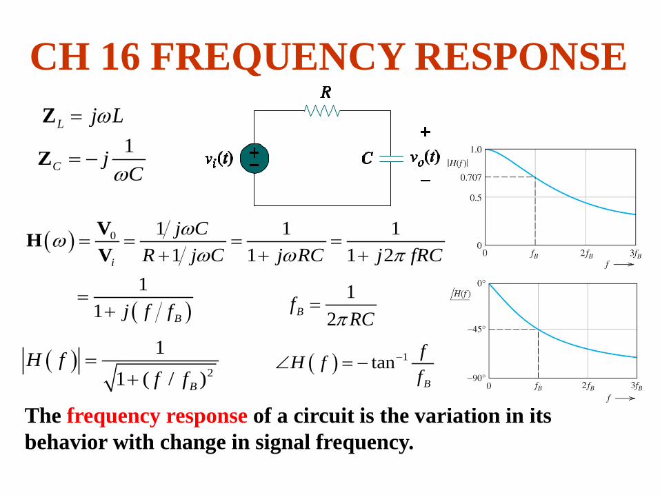
CH 16 FREQUENCY RESPONSE
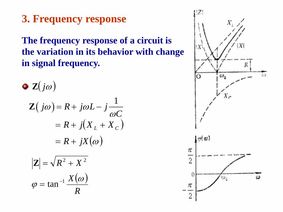
The frequency response of a circuit is the variation in its behavior with change in signal frequency.
L j Lω=Z1
C jCω
= −Z
( )
( )
0 1 1 11 1 1 2
1 1
i
B
j CR j C j RC j fRC
j f f
ωωω ω π
= = = =+ + +
=+
VHV
( )2
11 ( / )B
H ff f
=+
12Bf RCπ
=
( ) 1tanB
fH ff
−∠ = −
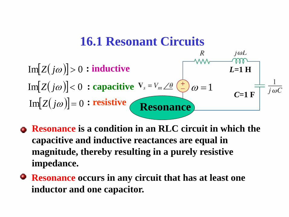
16.1 Resonant Circuits
( )[ ] 0Im >ωjZ : inductive
( )[ ] 0Im <ωjZ : capacitive
( )[ ] 0Im =ωjZ : resistive
Resonance occurs in any circuit that has at least one inductor and one capacitor.
Resonance is a condition in an RLC circuit in which the capacitive and inductive reactances are equal in magnitude, thereby resulting in a purely resistive impedance.
1=ω
L=1 H
C=1 FResonance
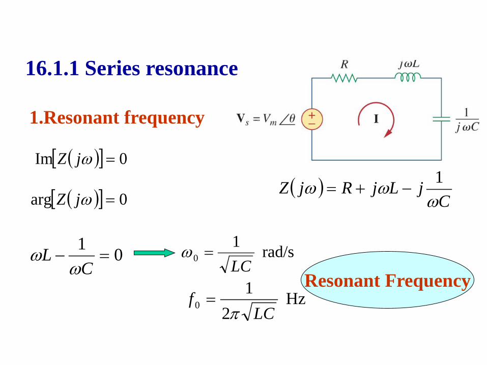
16.1.1 Series resonance
1.Resonant frequency
( )[ ] 0Im =ωjZ
( )[ ] 0arg =ωjZ( )
CjLjRjZω
ωω 1−+=
01=−
CL
ωω rad/s 1
0 LC=ω
Hz 2
10 LC
fπ
=Resonant Frequency
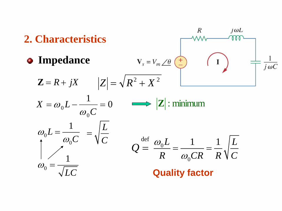
2. Characteristics
Impedance
minimum:Z01
00 =−=
CLX
ωω
00
1LC
ωω
=def
Q =
Quality factor
0
0
1 1L LR CR R Cω
ω= =
R jX= +Z 22 XRZ +=
01 LC
ω =
LC
=
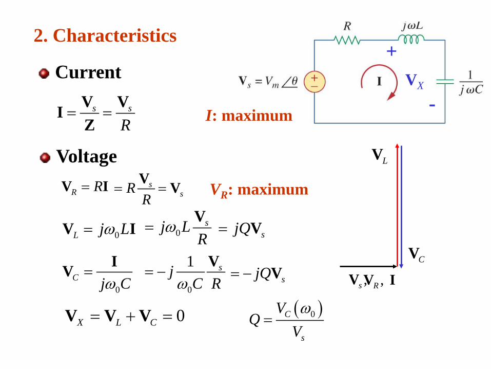
2. Characteristics
Current
s s
R= =
V VIZ I: maximum
Voltage s
sRR
= =V V
0L j Lω=V I
0C j Cω=
IV
0X L C= + =V V V ( )0C
s
VQ
Vω
=
, RV I,sV
LV
CV
R R=V I
0sj L
Rω=
VsjQ= V
0
1 sjC Rω
= −V
sjQ= − V
VR: maximum
+
-VX
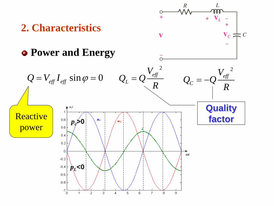
2. Characteristics
Power and Energy
sin 0eff effQ V I ϕ= =2
effL
VQ Q
R=
2eff
C
VQ Q
R= −
pL<0
pc>0Reactive power
Quality factor
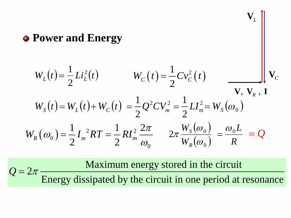
Power and Energy
( ) ( )tLitW LL2
21
= ( ) ( )212C CW t Cv t=
( ) ( ) ( )tWtWtW CLS +=
( ) 2 20
0
1 1 22 2R m mW I RT RI πω
ω= =
( )( )0
02ωω
πR
S
WW
Maximum energy stored in the circuit2Energy dissipated by the circuit in one period at resonance
Q π=
LV
CV
RV,V , I
( )0ωSW=
Q=R
L0ω=
2 2 21 12 2m mQ CV LI= =
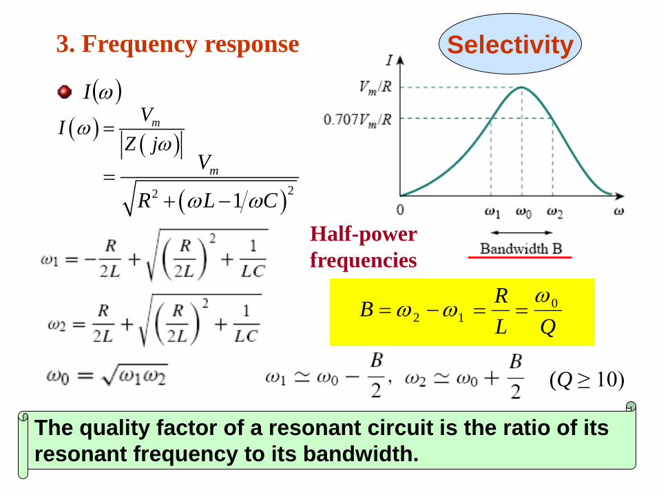
3. Frequency response
The frequency response of a circuit is the variation in its behavior with change in signal frequency.
( )ωjZ
( ) 1j R j L jC
ω ωω
= + −Z
22 XR +=Z
( )R
X ωϕ 1tan −=
( )CL XXjR ++=
( )ωjXR +=
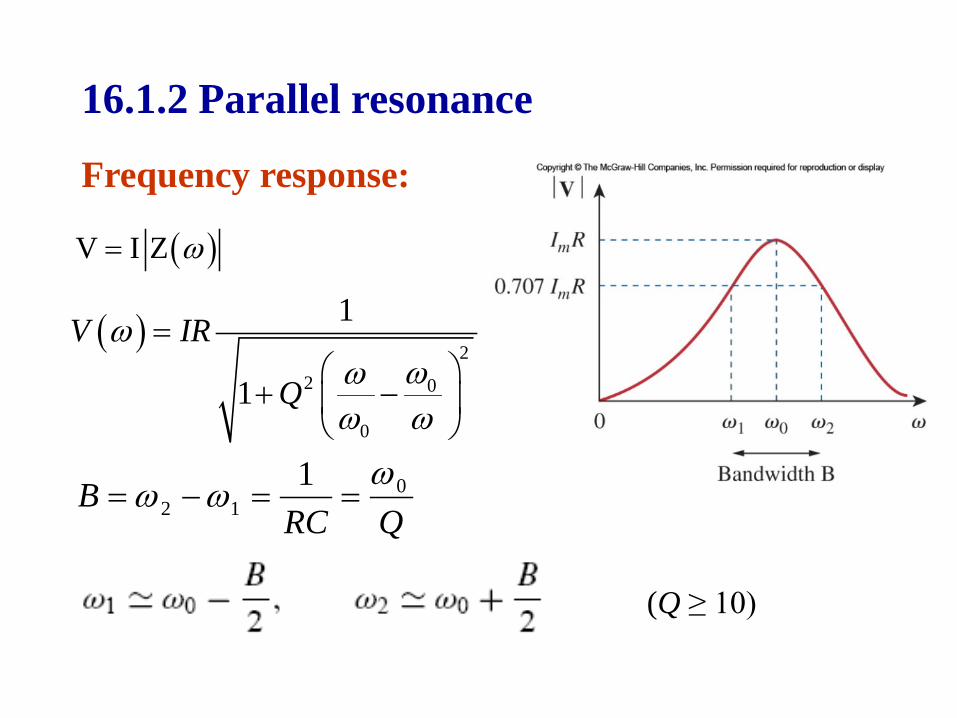
(Q ≥ 10)
3. Frequency response
( )ωI
( ) ( )mVI
Z jω
ω=
12 ωω −=B
( )22 1mV
R L Cω ω=
+ −
Half-power frequencies
The quality factor of a resonant circuit is the ratio of its resonant frequency to its bandwidth.
Selectivity
QLR 0ω==
( )( )22 1
mVIR L C
ωω ω
=+ −
22 2 2 0
0
mV
R Q R ωωω ω
=
+ −
22 0
0
1
1
mVR
Q ωωω ω
=
+ −
2
0
0
2
0
1
1
−+
=
ωω
ωωQ
I
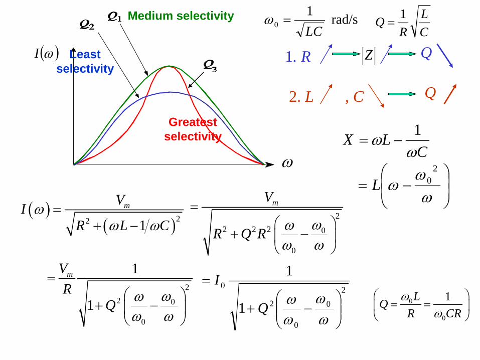
ω
( )ωI 1. R
Q2. L , C
CLX
ωω 1
−=
−=
ωω
ω2
0L
QZ
Medium selectivity
Least selectivity
Greatest selectivity
1 LQR C
=rad/s 10 LC=ω
0
0
1LQR CRω
ω
= =
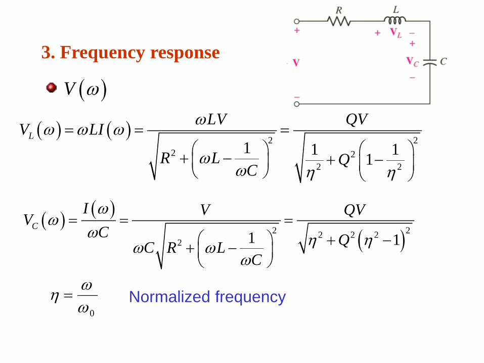
( )V ω
3. Frequency response
( ) ( )2 2
2 22 2
1 1 11L
LV QVV LI
R L QC
ωω ω ω
ωω η η
= = = + − + −
( ) ( )
( )2 22 2 22 1 1
C
I V QVVC QC R L
C
ωω
ω η ηω ωω
= = = + −+ −
0ωωη = Normalized frequency
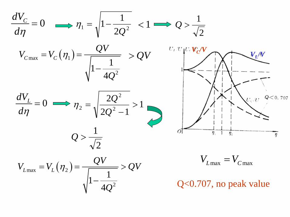
0CdVdη
=
0LdVdη
=
max maxL CV V=
Q<0.707, no peak value
21 211 Q
−=η 1<2
1 >Q
( )max 1
211
4
C CQVV V
Q
η= =−
QV>
112
22
2
2 >−
=Q
Qη
( )max 2
211
4
L LQVV V QV
Q
η= = >−
21 >Q
VC/VVL/V
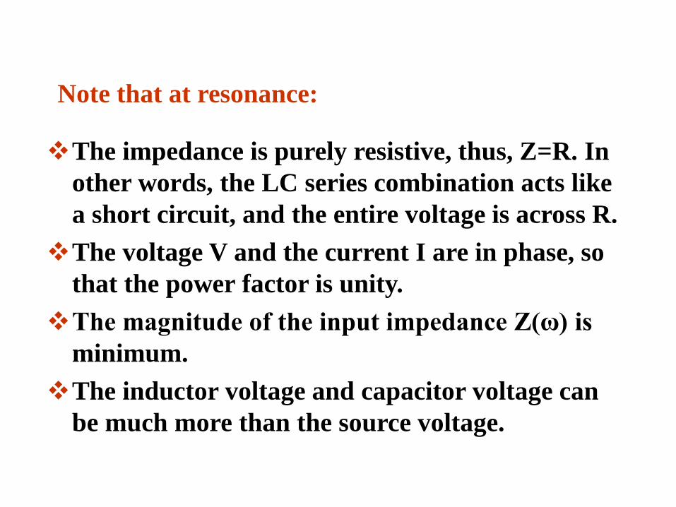
Note that at resonance:
The impedance is purely resistive, thus, Z=R. In other words, the LC series combination acts like a short circuit, and the entire voltage is across R.
The voltage V and the current I are in phase, so that the power factor is unity.
The magnitude of the input impedance Z(ω) is minimum.
The inductor voltage and capacitor voltage can be much more than the source voltage.
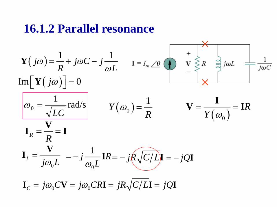
16.1.2 Parallel resonance
( ) 1 1j j C jR L
ω ωω
= + −Y
( )Im 0jω = Y
rad/s10 LC=ω ( )0
1YR
ω =
R R= =
VI I
jR C L= − I
( )0
RY ω
= =IV I
0L j Lω=
VI jQ= − I
0 0C j C j CR jR C L jQω ω= = = =I V I I I
0
1j RLω
= − I
×
×
( )2
2 0
0
1
1
V IR
Q
ωωω
ω ω
=
+ −
QRCB 0
121 ω
ωω ==−=
( )V I Z ω=
16.1.2 Parallel resonance
Frequency response:
(Q ≥ 10)
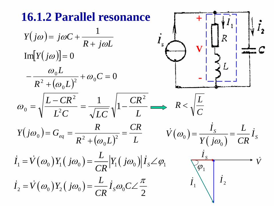
16.1.2 Parallel resonance
( )[ ] 0Im =ωjY
( )LjR
CjjYω
ωω+
+=1
( )002
02
0 =++
− CLR
Lω
ωω
LCR
LCCLCRL 2
2
2
0 11−=
−=ω C
LR <
( )( ) L
CRLR
RGjY eq =+
== 20
20 ωω ( ) ( )0
0
SS
I LV IY j CR
ωω
= =
( ) ( )2 0 2 0 0 2SLI V Y j I C
CRπω ω ω= = ∠
( ) ( ) ( )1 0 1 0 1 0 1SLI V Y j Y j I
CRω ω ω ϕ= = ∠
SIV
1I 2I1ϕ
+
-
V
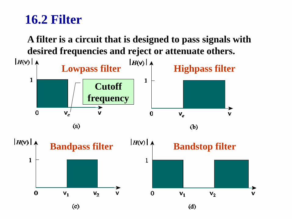
16.2 FilterA filter is a circuit that is designed to pass signals with desired frequencies and reject or attenuate others.
Lowpass filter Highpass filter
Cutoff frequency
Bandpass filter Bandstop filter
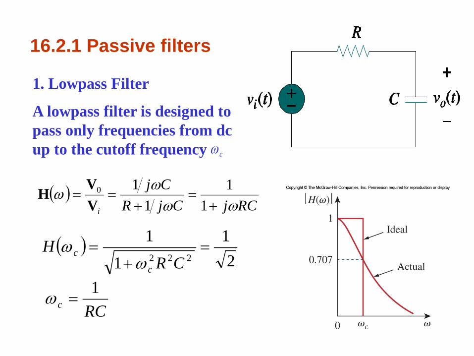
16.2.1 Passive filters
1. Lowpass Filter
( )RCjCjR
Cj
i ωωωω
+=
+==
11
110
VV
H
( )2
11
1222=
+=
CRH
c
cω
ω
RCc1
=ω
A lowpass filter is designed to pass only frequencies from dc up to the cutoff frequency cω
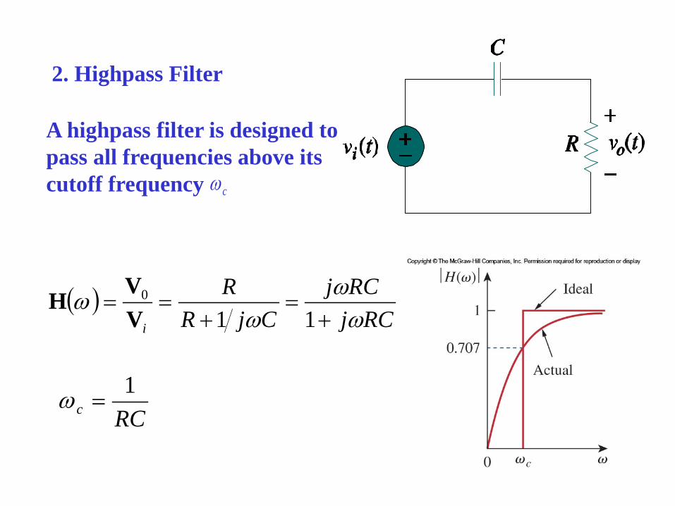
2. Highpass Filter
( )RCj
RCjCjR
R
i ωω
ωω
+=
+==
110
VV
H
RCc1
=ω
A highpass filter is designed to pass all frequencies above its cutoff frequency cω
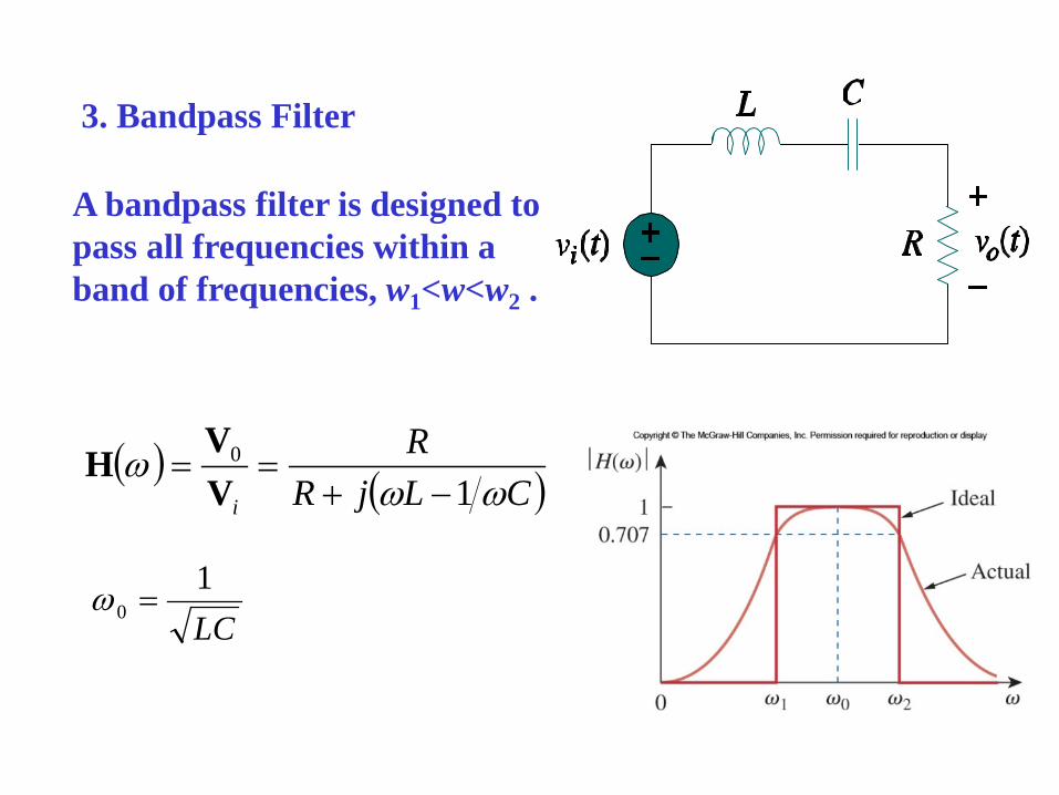
3. Bandpass Filter
A bandpass filter is designed to pass all frequencies within a band of frequencies, w1<w<w2 .
( ) ( )CLjRR
i ωωω
10
−+==
VV
H
LC1
0 =ω
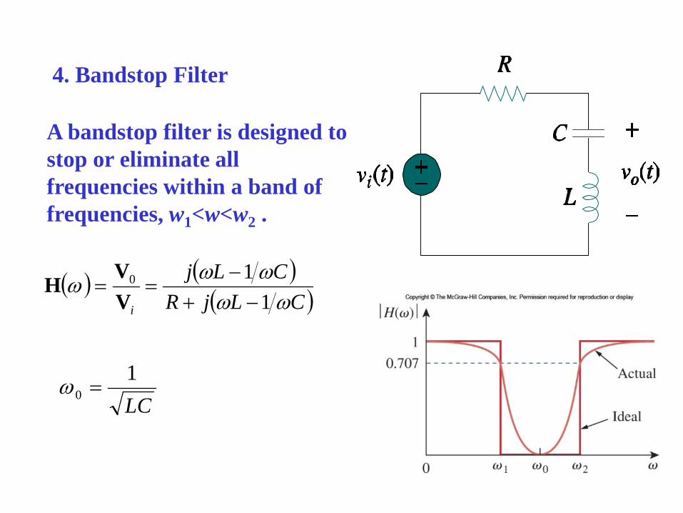
4. Bandstop Filter
A bandstop filter is designed to stop or eliminate all frequencies within a band of frequencies, w1<w<w2 .
( ) ( )( )CLjR
CLj
i ωωωωω1
10
−+−
==VV
H
LC1
0 =ω
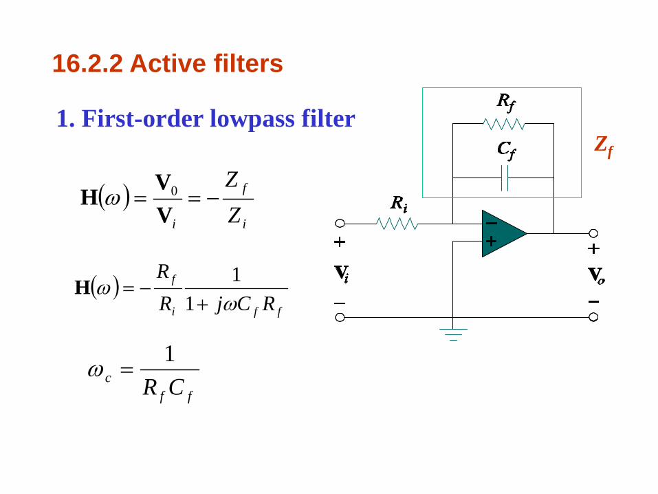
16.2.2 Active filters
1. First-order lowpass filterZf
( )i
f
i ZZ
−==VV
H 0ω
( )ffi
f
RCjRR
ωω
+−=
11H
ffc CR
1=ω
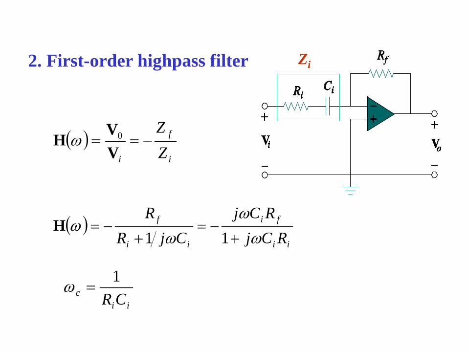
2. First-order highpass filter Zi
( )i
f
i ZZ
−==VV
H 0ω
( )ii
fi
ii
f
RCjRCj
CjRR
ωω
ωω
+−=
+−=
11H
iic CR
1=ω
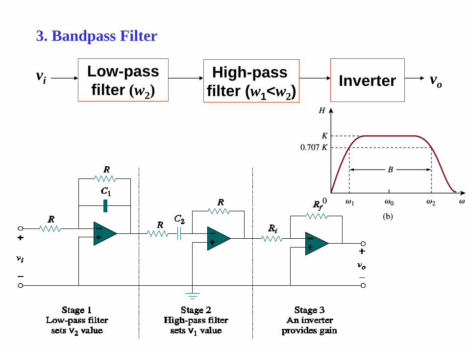
3. Bandpass Filter
Low-pass filter (w2)
High-pass filter (w1<w2)
Invertervi vo
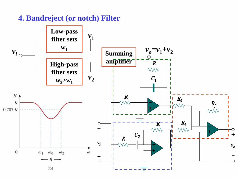
4. Bandreject (or notch) FilterLow-pass filter sets
w1
High-pass filter sets
w2>w1
Summing amplifier
vivo=v1+v2
v1
v2