Embed Size (px)
Citation preview
VLSI Design
3-
Chih-Cheng Hsieh
MOS Transistor Theory
CHAPTER 3
VLSI Design
3-
Chih-Cheng Hsieh
Outline 2
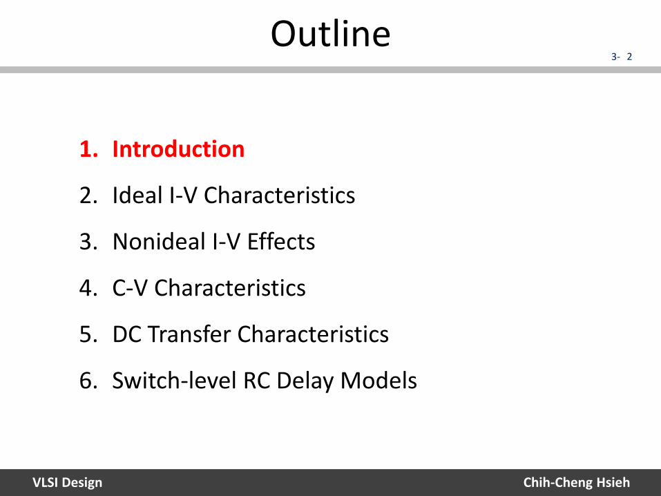
1. Introduction
2. Ideal I-V Characteristics
3. Nonideal I-V Effects
4. C-V Characteristics
5. DC Transfer Characteristics
6. Switch-level RC Delay Models
VLSI Design
3-
Chih-Cheng Hsieh
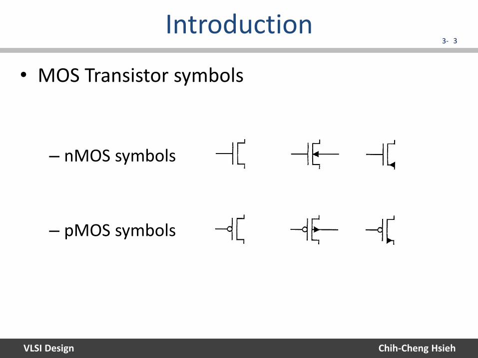
Introduction 3
• MOS Transistor symbols
– nMOS symbols
– pMOS symbols
VLSI Design
3-
Chih-Cheng Hsieh
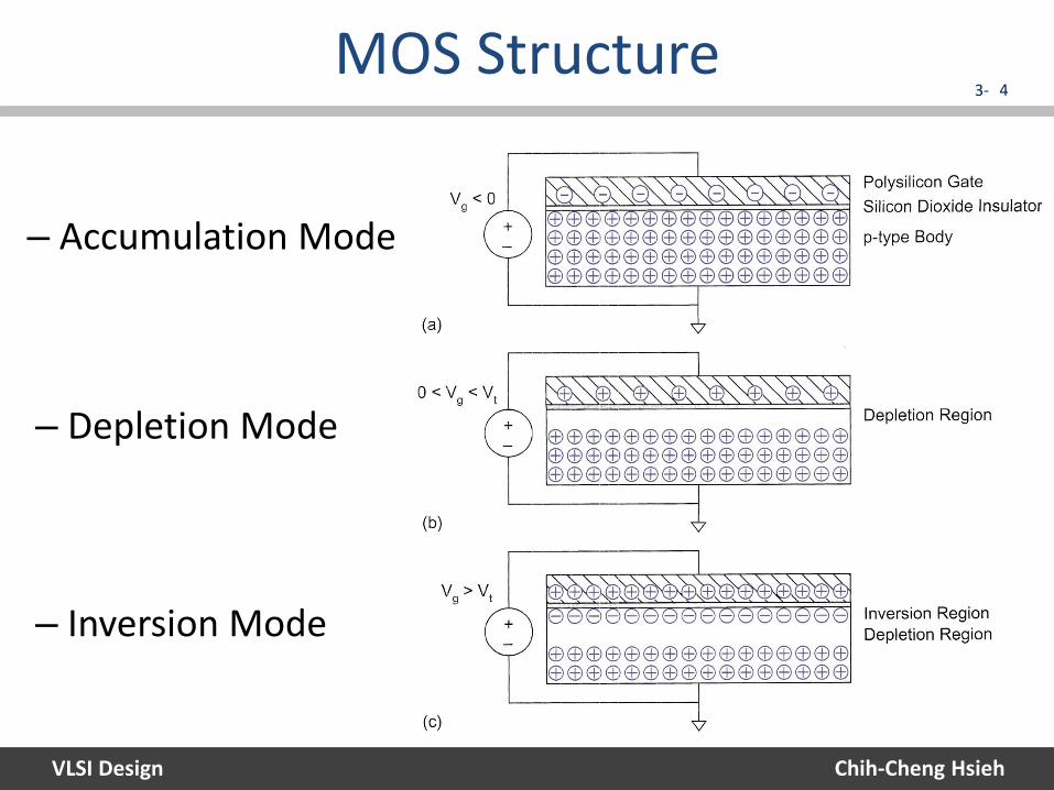
MOS Structure 4
– Accumulation Mode
– Depletion Mode
– Inversion Mode
VLSI Design
3-
Chih-Cheng Hsieh
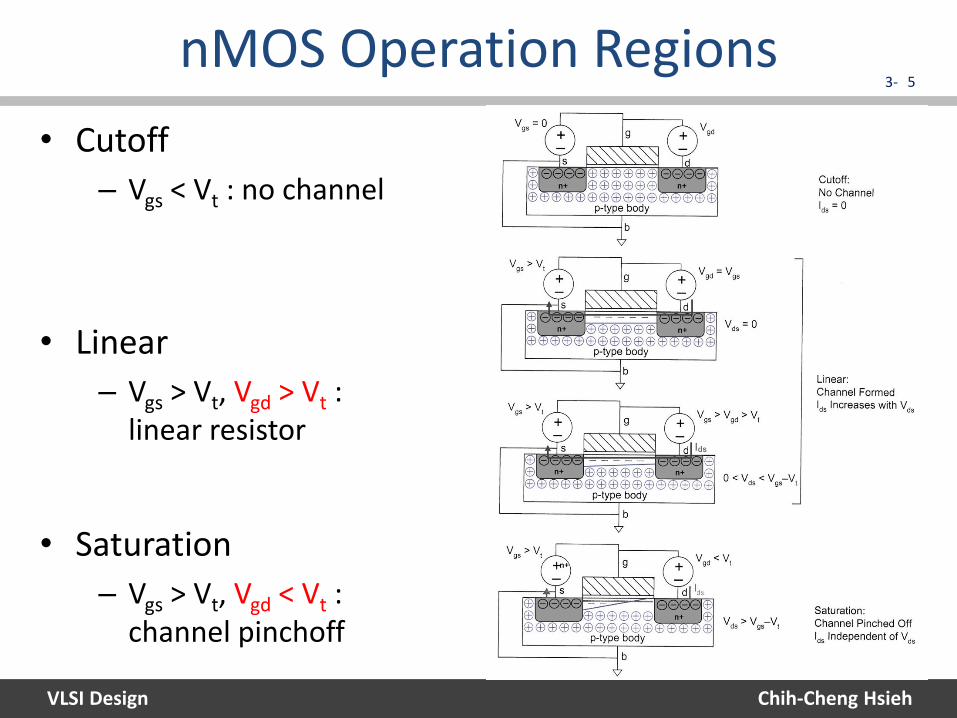
nMOS Operation Regions 5
• Cutoff
– Vgs < Vt : no channel
• Linear
– Vgs > Vt, Vgd > Vt : linear resistor
• Saturation
– Vgs > Vt, Vgd < Vt : channel pinchoff
VLSI Design
3-
Chih-Cheng Hsieh
6
1. Introduction
2. Ideal I-V Characteristics
3. Nonideal I-V Effects
4. C-V Characteristics
5. DC Transfer Characteristics
6. Switch-level RC Delay Models
Outline
VLSI Design
3-
Chih-Cheng Hsieh
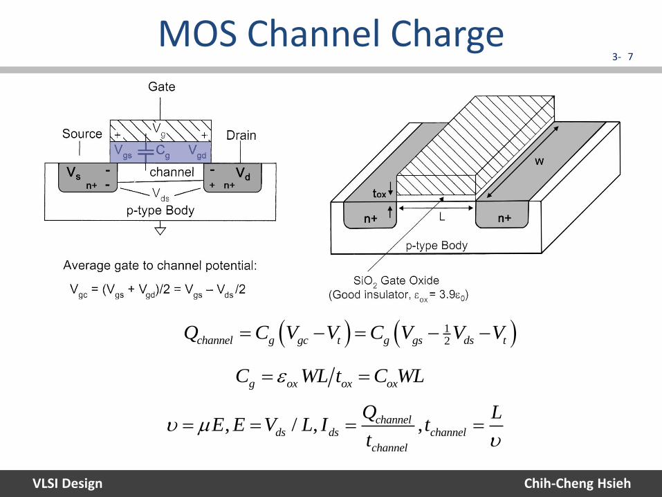
MOS Channel Charge 7
12channel g gc t g gs ds tQ C V V C V V V
g ox ox oxC WL t C WL
, / , ,channelds ds channel
channel
Q LE E V L I t
t
VLSI Design
3-
Chih-Cheng Hsieh
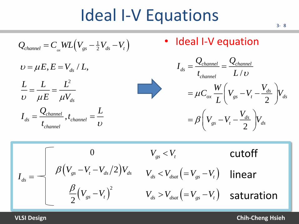
Ideal I-V Equations 8
12oxchannel gs ds tQ C WL V V V
/
2
2
channel channelds
channel
dsox gs t ds
dsgs t ds
Q QI
t L
VWC V V V
L
VV V V
2
,
ds
channelds channel
channel
L L L
E V
Q LI t
t
, / ,dsE E V L
2
2gs tV V
• Ideal I-V equation
2gs t ds dsV V V V
0
dsI
gs tV V
ds dsat gs tV V V V
cutoff
linear
saturation ds dsat gs tV V V V
VLSI Design
3-
Chih-Cheng Hsieh
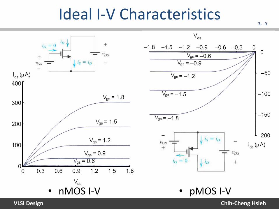
Ideal I-V Characteristics 9
• nMOS I-V • pMOS I-V
VLSI Design
3-
Chih-Cheng Hsieh
Outline 10
1. Introduction
2. Ideal I-V Characteristics
3. Nonideal I-V Effects
4. C-V Characteristics
5. DC Transfer Characteristics
6. Switch-level RC Delay Models
VLSI Design
3-
Chih-Cheng Hsieh
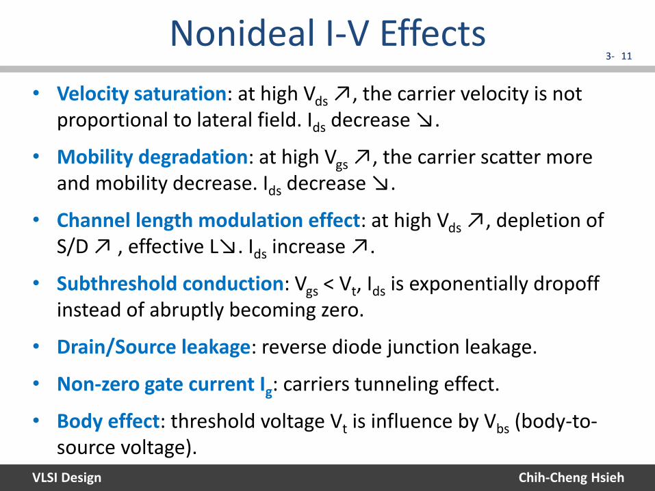
Nonideal I-V Effects 11
• Velocity saturation: at high Vds ↗, the carrier velocity is not proportional to lateral field. Ids decrease ↘.
• Mobility degradation: at high Vgs ↗, the carrier scatter more and mobility decrease. Ids decrease ↘.
• Channel length modulation effect: at high Vds ↗, depletion of S/D ↗ , effective L↘. Ids increase ↗.
• Subthreshold conduction: Vgs < Vt, Ids is exponentially dropoff instead of abruptly becoming zero.
• Drain/Source leakage: reverse diode junction leakage.
• Non-zero gate current Ig: carriers tunneling effect.
• Body effect: threshold voltage Vt is influence by Vbs (body-to-source voltage).
VLSI Design
3-
Chih-Cheng Hsieh
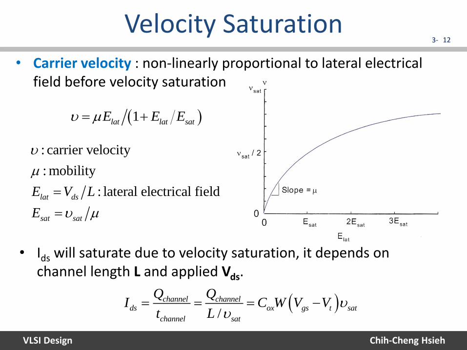
Velocity Saturation 12
1lat lat satE E E
: carrier velocity
: mobility
: lateral electrical fieldlat ds
sat sat
E V L
E
• Carrier velocity : non-linearly proportional to lateral electrical field before velocity saturation
/
channel channelds ox gs t sat
channel sat
Q QI C W V V
t L
• Ids will saturate due to velocity saturation, it depends on channel length L and applied Vds.
VLSI Design
3-
Chih-Cheng Hsieh
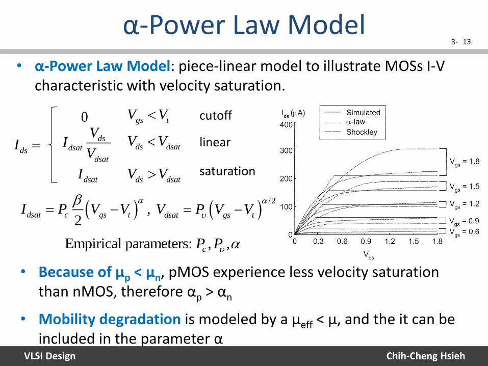
α-Power Law Model 13
dsatI
dsdsat
dsat
VI
V
0
dsI
gs tV V
ds dsatV V
ds dsatV V
cutoff
linear
saturation
,2
dsat c gs tI P V V
/2
dsat gs tV P V V
• α-Power Law Model: piece-linear model to illustrate MOSs I-V characteristic with velocity saturation.
• Because of μp < μn, pMOS experience less velocity saturation than nMOS, therefore αp > αn
• Mobility degradation is modeled by a μeff < μ, and the it can be included in the parameter α
Empirical parameters: , ,cP P
VLSI Design
3-
Chih-Cheng Hsieh
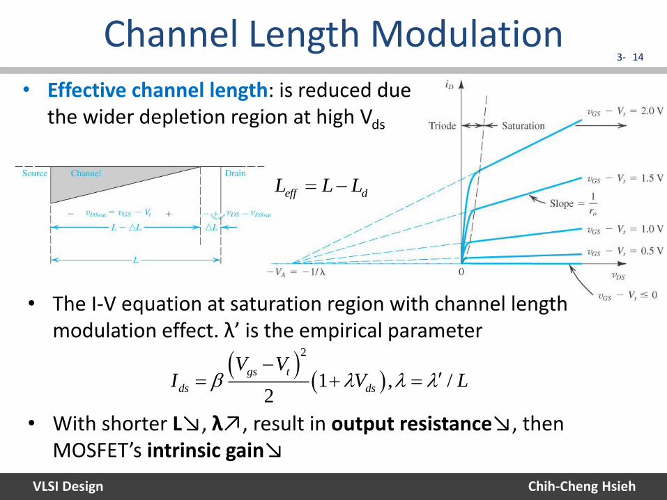
Channel Length Modulation 14
eff dL L L
• Effective channel length: is reduced due the wider depletion region at high Vds
2
1 , /2
gs t
ds ds
V VI V L
• The I-V equation at saturation region with channel length modulation effect. λ’ is the empirical parameter
• With shorter L↘, λ↗, result in output resistance↘, then MOSFET’s intrinsic gain↘
VLSI Design
3-
Chih-Cheng Hsieh
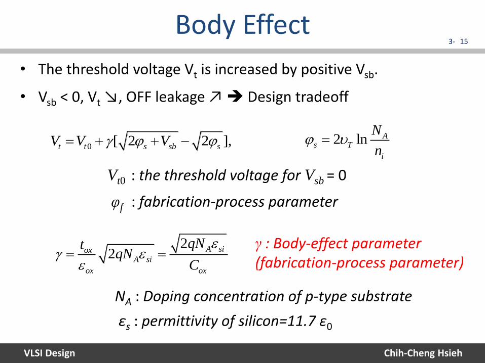
Body Effect 15
NA : Doping concentration of p-type substrate
εs : permittivity of silicon=11.7 ε0
γ : Body-effect parameter (fabrication-process parameter)
0 [ 2 2 ],t t s sb sV V V 2 ln As T
i
N
n
22
A sioxA si
ox ox
qNtqN
C
Vt0 : the threshold voltage for Vsb = 0
φf : fabrication-process parameter
• The threshold voltage Vt is increased by positive Vsb.
• Vsb < 0, Vt ↘, OFF leakage ↗ Design tradeoff
VLSI Design
3-
Chih-Cheng Hsieh
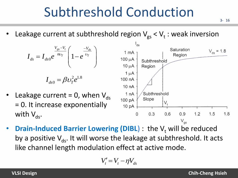
Subthreshold Conduction 16
0 1
gs t ds
T T
V V V
n
ds dsI I e e
• Leakage current at subthreshold region Vgs < Vt : weak inversion
2 1.8
0ds TI e
• Leakage current = 0, when Vds = 0. It increase exponentially with Vds.
• Drain-Induced Barrier Lowering (DIBL) : the Vt will be reduced by a positive Vds. It will worse the leakage at subthreshold. It acts like channel length modulation effect at active mode.
t t dsV V V
VLSI Design
3-
Chih-Cheng Hsieh
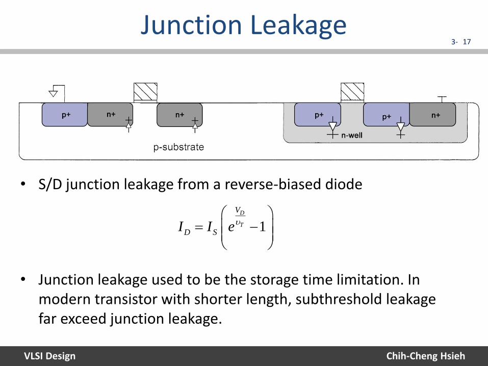
Junction Leakage 17
1D
T
V
D SI I e
• S/D junction leakage from a reverse-biased diode
• Junction leakage used to be the storage time limitation. In modern transistor with shorter length, subthreshold leakage far exceed junction leakage.
VLSI Design
3-
Chih-Cheng Hsieh
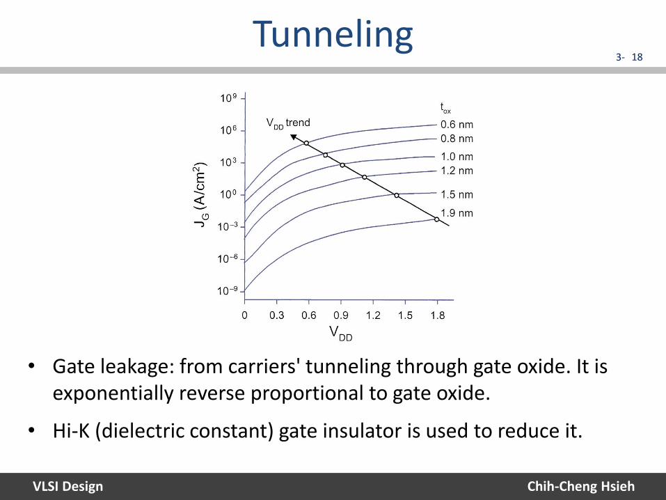
Tunneling 18
• Gate leakage: from carriers' tunneling through gate oxide. It is exponentially reverse proportional to gate oxide.
• Hi-K (dielectric constant) gate insulator is used to reduce it.
VLSI Design
3-
Chih-Cheng Hsieh
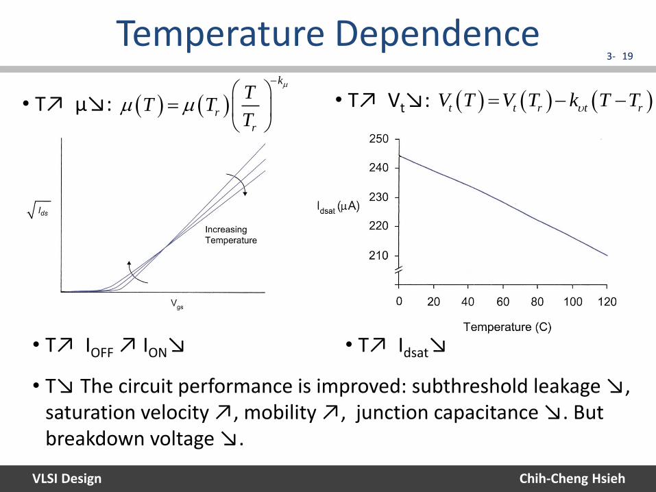
Temperature Dependence 19
k
r
r
TT T
T
t t r t rV T V T k T T • T↗ μ↘: • T↗ Vt↘:
• T↗ IOFF ↗ ION↘ • T↗ Idsat↘
• T↘ The circuit performance is improved: subthreshold leakage ↘, saturation velocity ↗, mobility ↗, junction capacitance ↘. But breakdown voltage ↘.
VLSI Design
3-
Chih-Cheng Hsieh
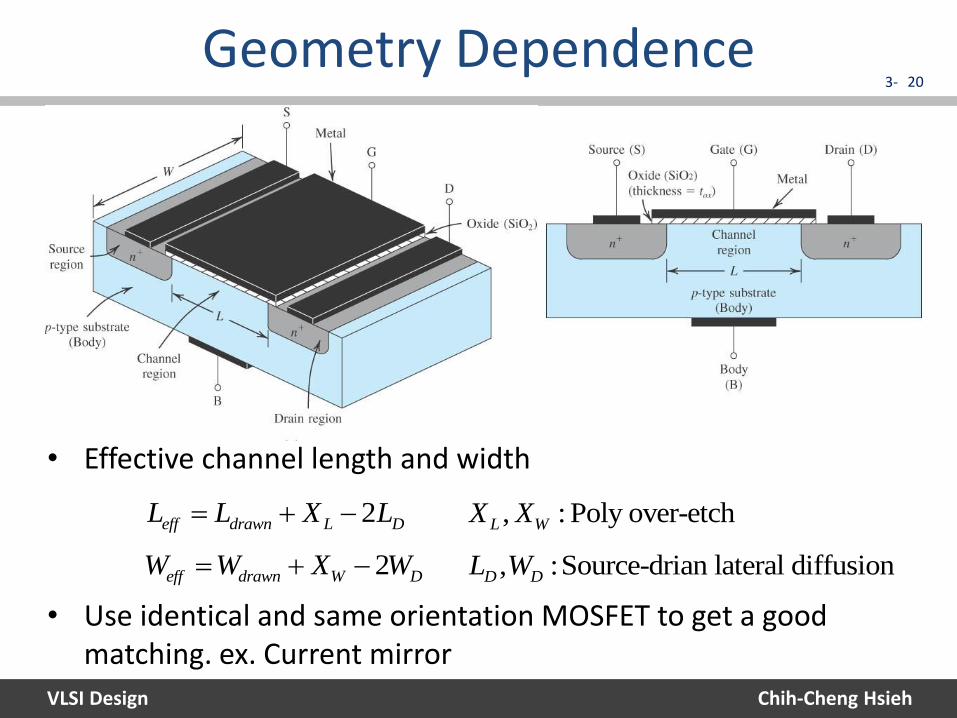
Geometry Dependence 20
• Effective channel length and width
2eff drawn L DL L X L
2eff drawn W DW W X W
, : Poly over-etchL WX X
, :Source-drian lateral diffusionD DL W
• Use identical and same orientation MOSFET to get a good matching. ex. Current mirror
VLSI Design
3-
Chih-Cheng Hsieh
21
1. Introduction
2. Ideal I-V Characteristics
3. Nonideal I-V Effects
4. C-V Characteristics
5. DC Transfer Characteristics
6. Switch-level RC Delay Models
Outline
VLSI Design
3-
Chih-Cheng Hsieh
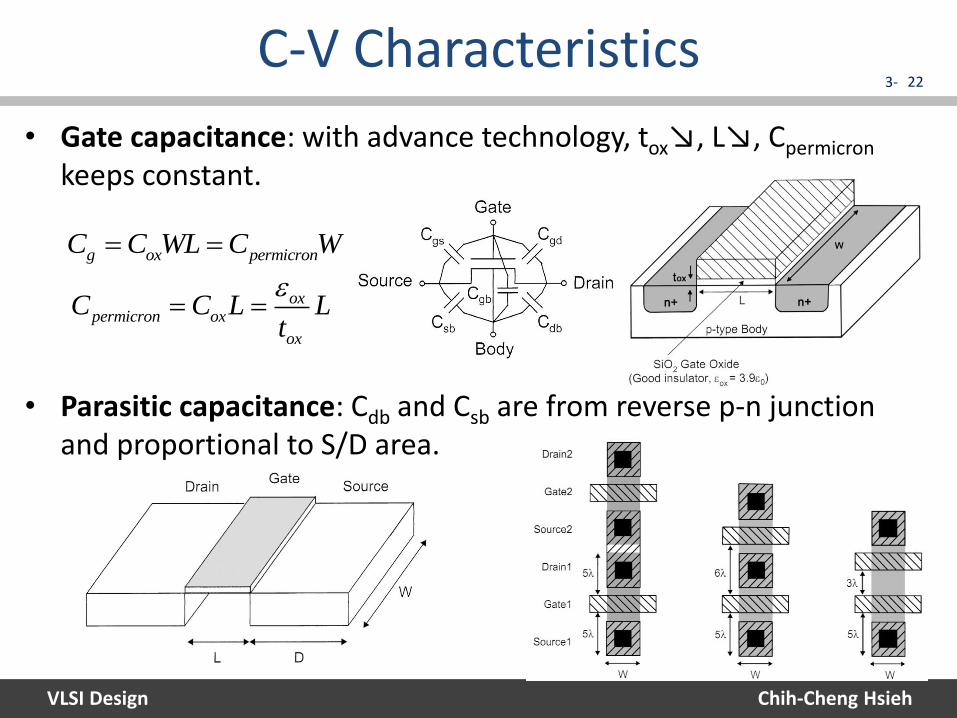
C-V Characteristics 22
g ox permicronC C WL C W
oxpermicron ox
ox
C C L Lt
• Gate capacitance: with advance technology, tox↘, L↘, Cpermicron keeps constant.
• Parasitic capacitance: Cdb and Csb are from reverse p-n junction and proportional to S/D area.
VLSI Design
3-
Chih-Cheng Hsieh
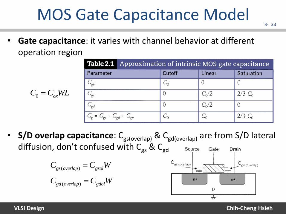
MOS Gate Capacitance Model 23
( )gs overlap gsolC C W
( )gd overlap gdolC C W
• S/D overlap capacitance: Cgs(overlap) & Cgd(overlap) are from S/D lateral diffusion, don’t confused with Cgs & Cgd
• Gate capacitance: it varies with channel behavior at different operation region
0 oxC C WL
VLSI Design
3-
Chih-Cheng Hsieh
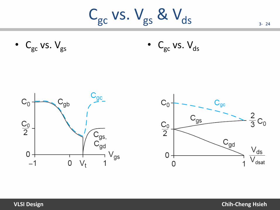
Cgc vs. Vgs & Vds 24
• Cgc vs. Vgs • Cgc vs. Vds
VLSI Design
3-
Chih-Cheng Hsieh
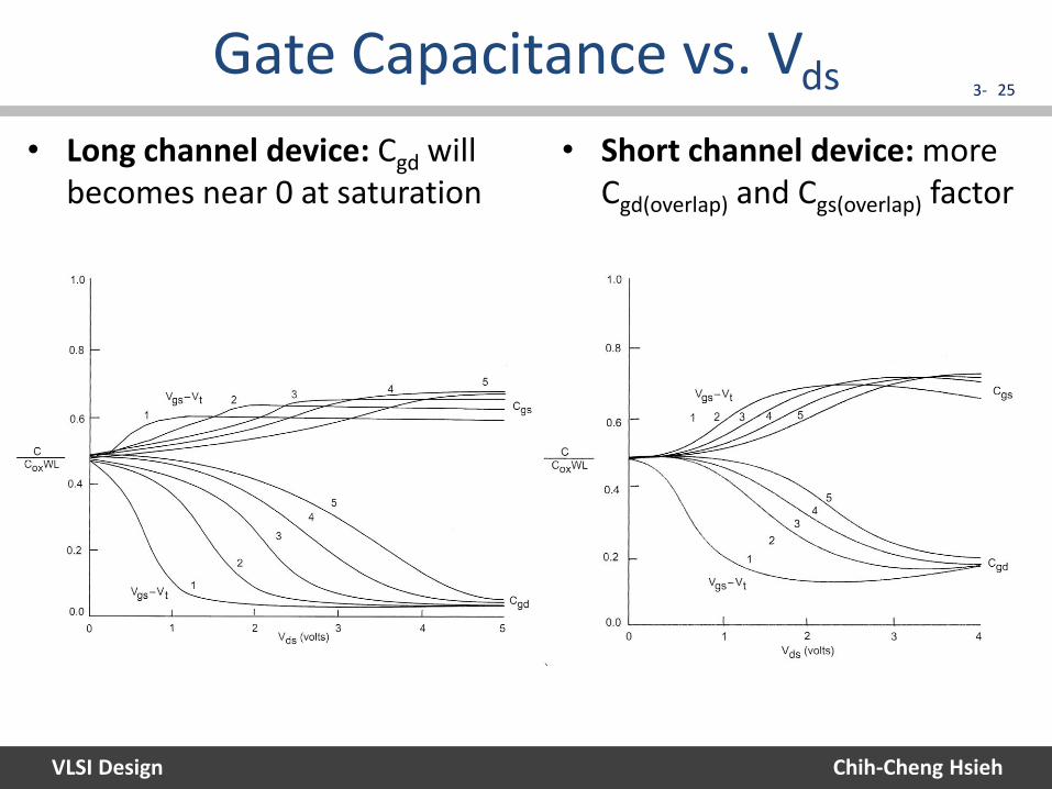
Gate Capacitance vs. Vds 25
• Long channel device: Cgd will becomes near 0 at saturation
• Short channel device: more Cgd(overlap) and Cgs(overlap) factor
VLSI Design
3-
Chih-Cheng Hsieh
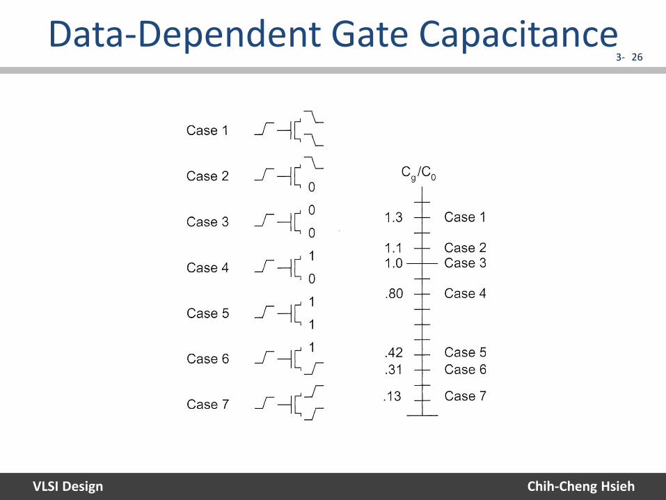
Data-Dependent Gate Capacitance 26
VLSI Design
3-
Chih-Cheng Hsieh
27
1. Introduction
2. Ideal I-V Characteristics
3. Nonideal I-V Effects
4. C-V Characteristics
5. DC Transfer Characteristics
6. Switch-level RC Delay Models
Outline
VLSI Design
3-
Chih-Cheng Hsieh
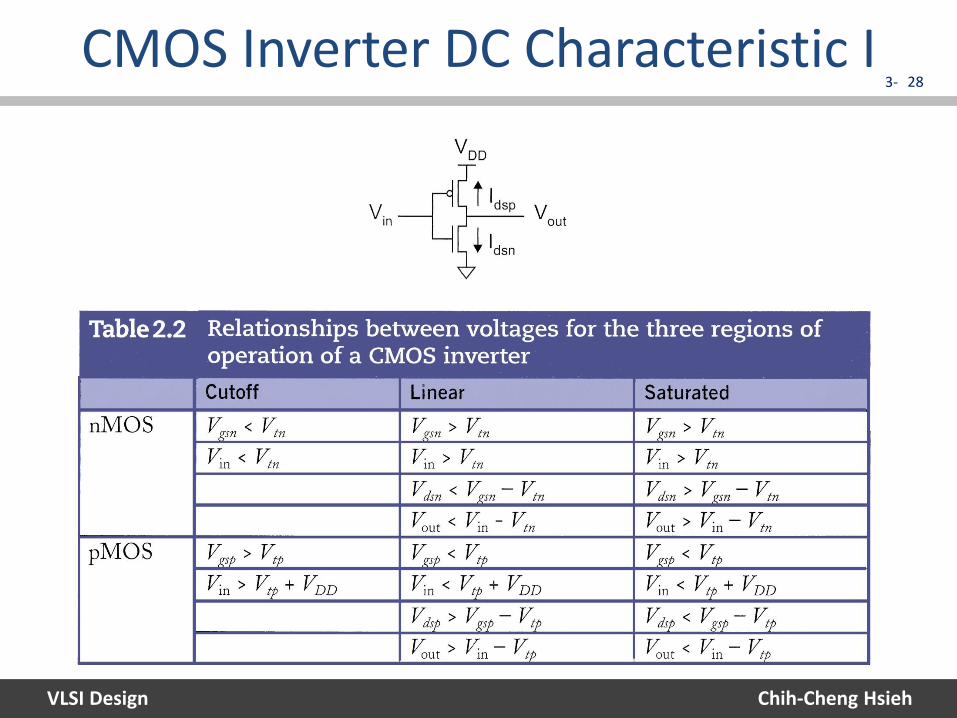
CMOS Inverter DC Characteristic I 28
VLSI Design
3-
Chih-Cheng Hsieh
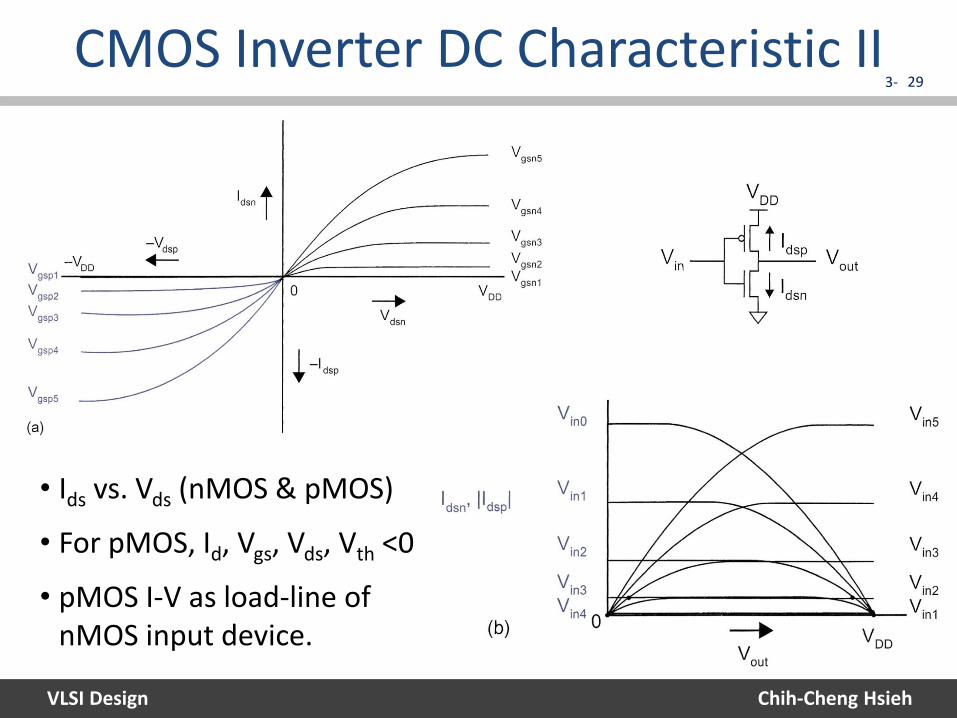
CMOS Inverter DC Characteristic II 29
• Ids vs. Vds (nMOS & pMOS)
• For pMOS, Id, Vgs, Vds, Vth <0
• pMOS I-V as load-line of nMOS input device.
VLSI Design
3-
Chih-Cheng Hsieh
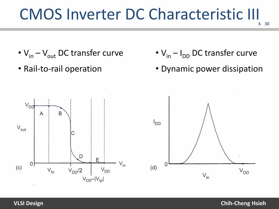
CMOS Inverter DC Characteristic III 30
• Vin – Vout DC transfer curve
• Rail-to-rail operation
• Vin – IDD DC transfer curve
• Dynamic power dissipation
VLSI Design
3-
Chih-Cheng Hsieh
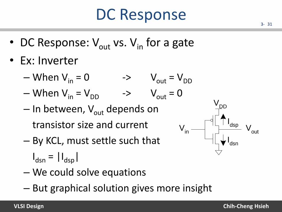
DC Response 31
• DC Response: Vout vs. Vin for a gate
• Ex: Inverter
– When Vin = 0 -> Vout = VDD
– When Vin = VDD -> Vout = 0
– In between, Vout depends on
transistor size and current
– By KCL, must settle such that
Idsn = |Idsp|
– We could solve equations
– But graphical solution gives more insight
Idsn
Idsp
Vout
VDD
Vin
VLSI Design
3-
Chih-Cheng Hsieh
Transistor Operation 32
• Current depends on region of transistor behavior
• For what Vin and Vout are nMOS and pMOS in
– Cutoff?
– Linear?
– Saturation?
VLSI Design
3-
Chih-Cheng Hsieh
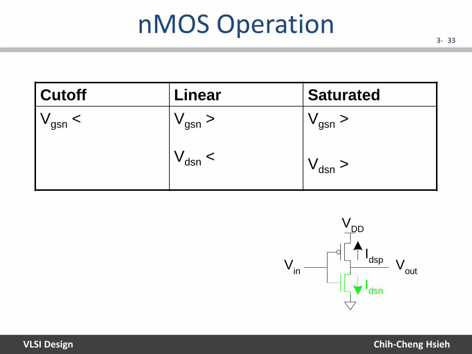
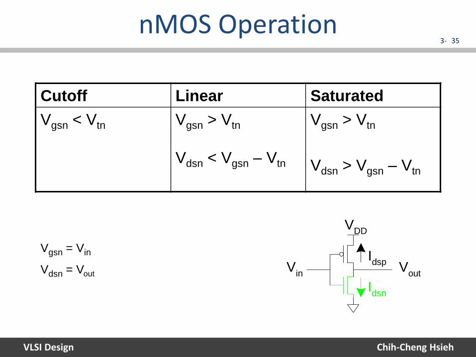
nMOS Operation 33
Cutoff Linear Saturated
Vgsn <
Vgsn >
Vdsn <
Vgsn >
Vdsn >
Idsn
Idsp
Vout
VDD
Vin
VLSI Design
3-
Chih-Cheng Hsieh
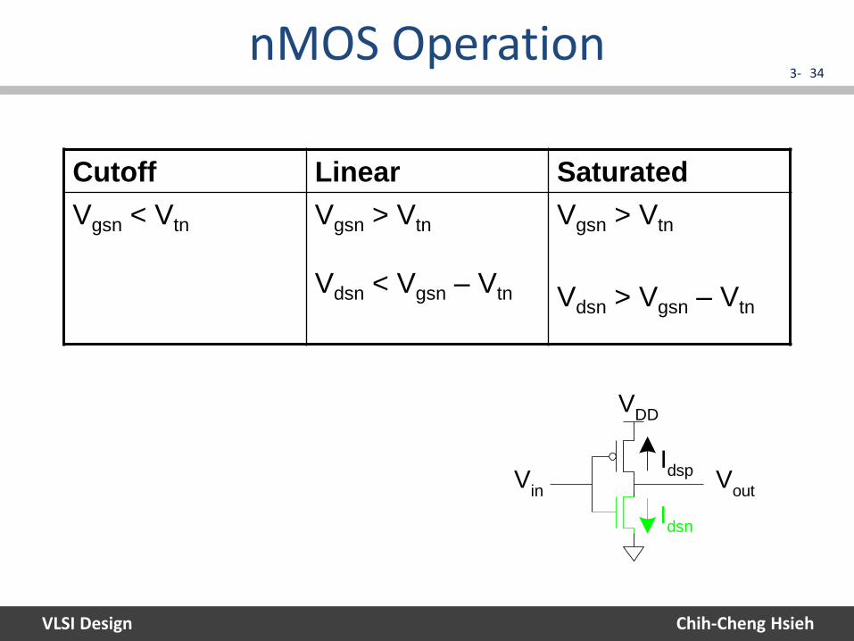
nMOS Operation 34
Cutoff Linear Saturated
Vgsn < Vtn
Vgsn > Vtn
Vdsn < Vgsn – Vtn
Vgsn > Vtn
Vdsn > Vgsn – Vtn
Idsn
Idsp
Vout
VDD
Vin
VLSI Design
3-
Chih-Cheng Hsieh
nMOS Operation 35
Cutoff Linear Saturated
Vgsn < Vtn
Vgsn > Vtn
Vdsn < Vgsn – Vtn
Vgsn > Vtn
Vdsn > Vgsn – Vtn
Idsn
Idsp
Vout
VDD
Vin
Vgsn = Vin
Vdsn = Vout
VLSI Design
3-
Chih-Cheng Hsieh
nMOS Operation 33
Cutoff Linear Saturated
Vgsn < Vtn
Vin < Vtn
Vgsn > Vtn
Vin > Vtn
Vdsn < Vgsn – Vtn
Vout < Vin - Vtn
Vgsn > Vtn
Vin > Vtn
Vdsn > Vgsn – Vtn
Vout > Vin - Vtn
Idsn
Idsp
Vout
VDD
Vin
Vgsn = Vin
Vdsn = Vout
VLSI Design
3-
Chih-Cheng Hsieh
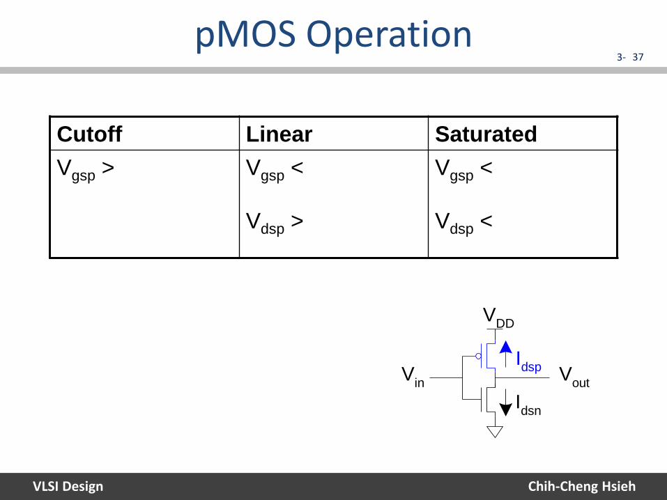
pMOS Operation 37
Cutoff Linear Saturated
Vgsp >
Vgsp <
Vdsp >
Vgsp <
Vdsp <
Idsn
Idsp
Vout
VDD
Vin
VLSI Design
3-
Chih-Cheng Hsieh
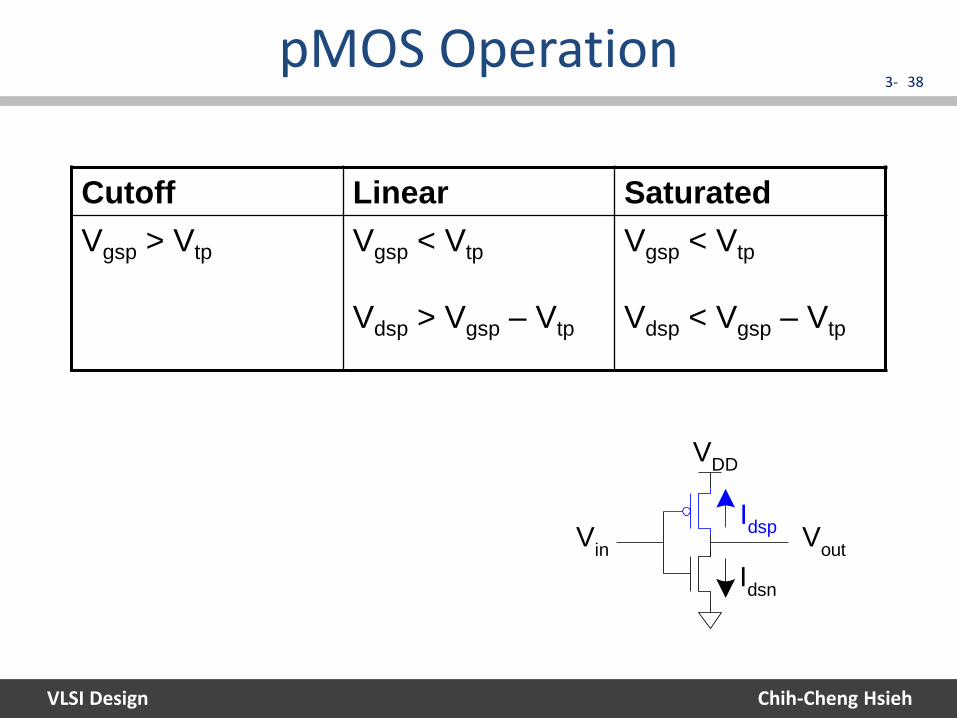
pMOS Operation 38
Cutoff Linear Saturated
Vgsp > Vtp
Vgsp < Vtp
Vdsp > Vgsp – Vtp
Vgsp < Vtp
Vdsp < Vgsp – Vtp
Idsn
Idsp
Vout
VDD
Vin
VLSI Design
3-
Chih-Cheng Hsieh
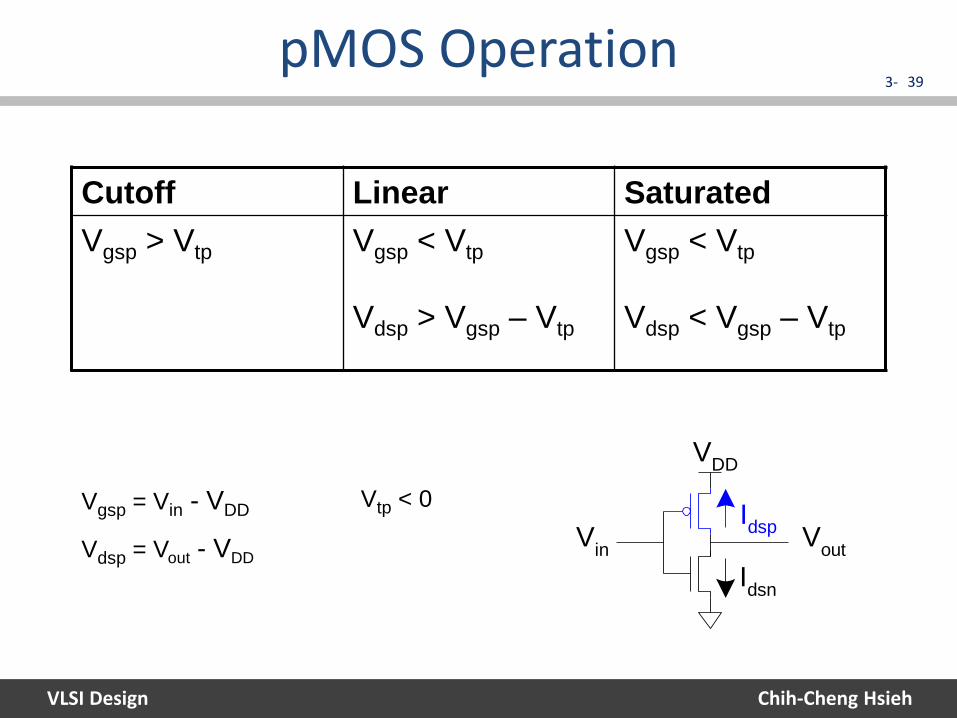
pMOS Operation 39
Cutoff Linear Saturated
Vgsp > Vtp
Vgsp < Vtp
Vdsp > Vgsp – Vtp
Vgsp < Vtp
Vdsp < Vgsp – Vtp
Idsn
Idsp
Vout
VDD
Vin
Vgsp = Vin - VDD
Vdsp = Vout - VDD
Vtp < 0
VLSI Design
3-
Chih-Cheng Hsieh
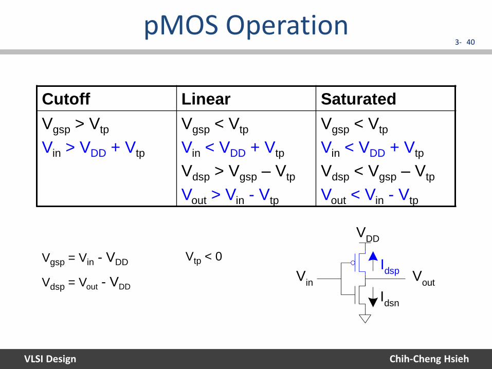
pMOS Operation 40
Cutoff Linear Saturated
Vgsp > Vtp
Vin > VDD + Vtp
Vgsp < Vtp
Vin < VDD + Vtp
Vdsp > Vgsp – Vtp
Vout > Vin - Vtp
Vgsp < Vtp
Vin < VDD + Vtp
Vdsp < Vgsp – Vtp
Vout < Vin - Vtp
Idsn
Idsp
Vout
VDD
Vin
Vgsp = Vin - VDD
Vdsp = Vout - VDD
Vtp < 0
VLSI Design
3-
Chih-Cheng Hsieh
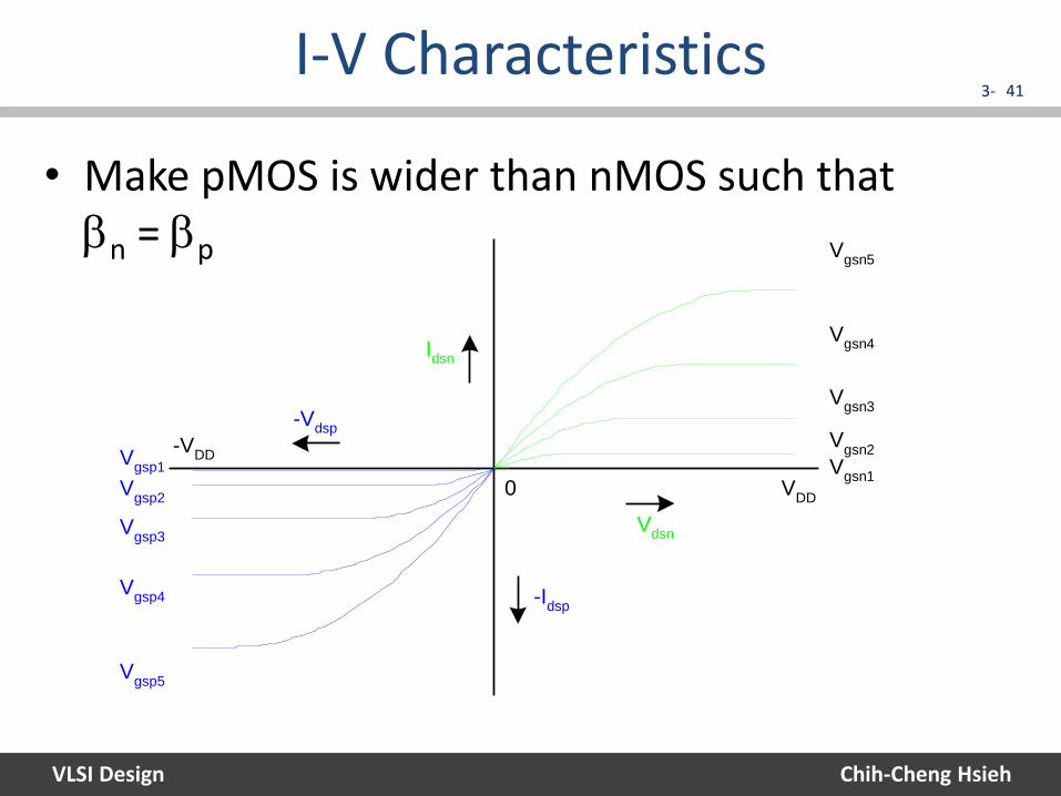
I-V Characteristics 41
• Make pMOS is wider than nMOS such that n = p V
gsn5
Vgsn4
Vgsn3
Vgsn2
Vgsn1
Vgsp5
Vgsp4
Vgsp3
Vgsp2
Vgsp1
VDD
-VDD
Vdsn
-Vdsp
-Idsp
Idsn
0
VLSI Design
3-
Chih-Cheng Hsieh
Current vs. Vout, Vin 42
Vin5
Vin4
Vin3
Vin2
Vin1
Vin0
Vin1
Vin2
Vin3
Vin4
Idsn
, |Idsp
|
Vout
VDD
VLSI Design
3-
Chih-Cheng Hsieh
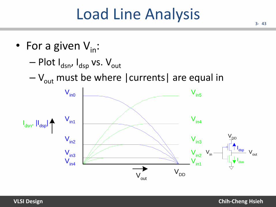
Load Line Analysis 43
• For a given Vin:
– Plot Idsn, Idsp vs. Vout
– Vout must be where |currents| are equal in
Vin5
Vin4
Vin3
Vin2
Vin1
Vin0
Vin1
Vin2
Vin3
Vin4
Idsn
, |Idsp
|
Vout
VDD
Idsn
Idsp
Vout
VDD
Vin
VLSI Design
3-
Chih-Cheng Hsieh
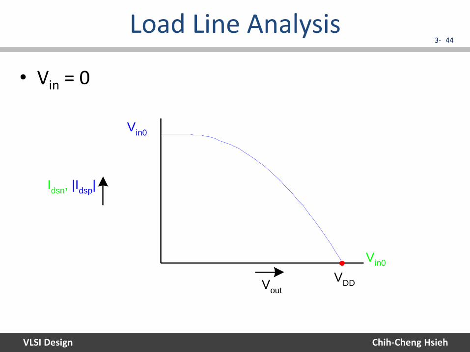
Load Line Analysis 44
• Vin = 0
Vin0
Vin0
Idsn
, |Idsp
|
Vout
VDD
VLSI Design
3-
Chih-Cheng Hsieh
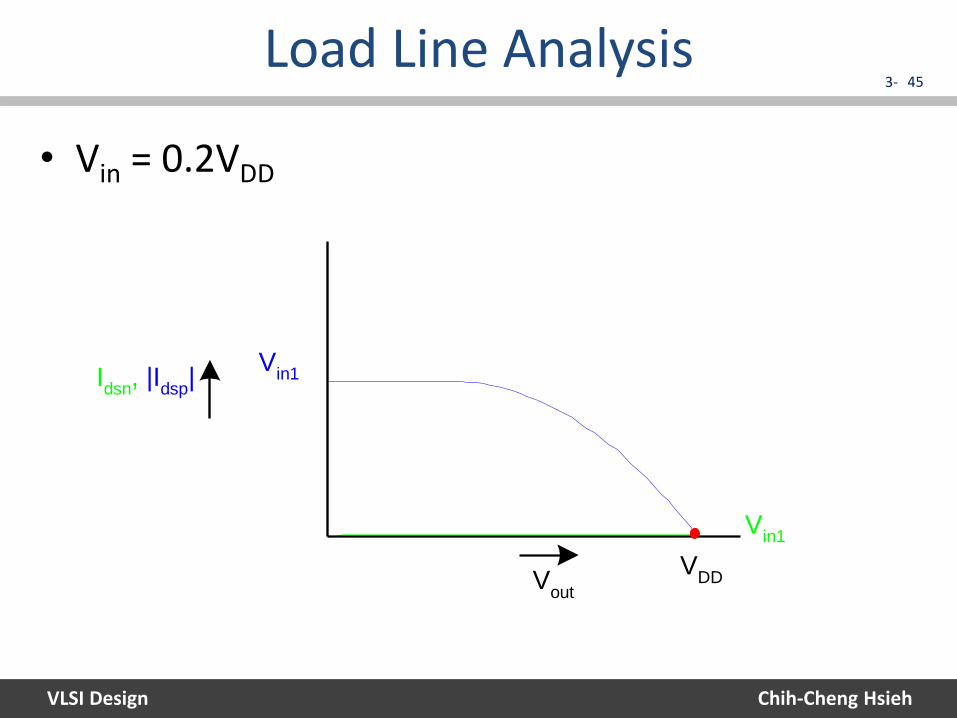
Load Line Analysis 45
• Vin = 0.2VDD
Vin1
Vin1I
dsn, |I
dsp|
Vout
VDD
VLSI Design
3-
Chih-Cheng Hsieh
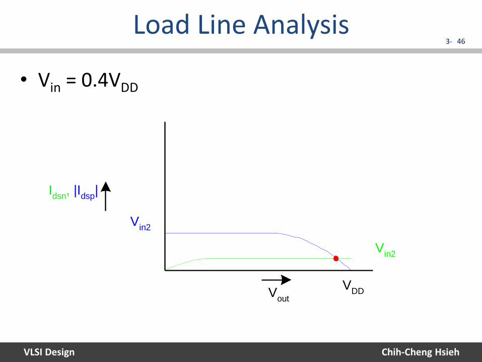
Load Line Analysis 46
• Vin = 0.4VDD
Vin2
Vin2
Idsn
, |Idsp
|
Vout
VDD
VLSI Design
3-
Chih-Cheng Hsieh
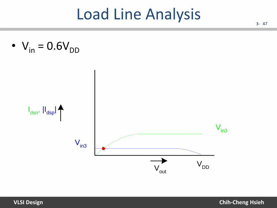
Load Line Analysis 47
• Vin = 0.6VDD
Vin3
Vin3
Idsn
, |Idsp
|
Vout
VDD
VLSI Design
3-
Chih-Cheng Hsieh
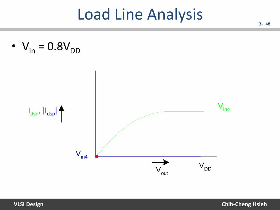
Load Line Analysis 48
• Vin = 0.8VDD
Vin4
Vin4
Idsn
, |Idsp
|
Vout
VDD
VLSI Design
3-
Chih-Cheng Hsieh
Load Line Analysis 49
• Vin = VDD
Vin5
Vin0
Vin1
Vin2
Vin3
Vin4
Idsn
, |Idsp
|
Vout
VDD
VLSI Design
3-
Chih-Cheng Hsieh
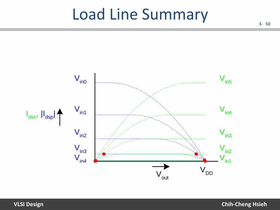
Load Line Summary 50
Vin5
Vin4
Vin3
Vin2
Vin1
Vin0
Vin1
Vin2
Vin3
Vin4
Idsn
, |Idsp
|
Vout
VDD
VLSI Design
3-
Chih-Cheng Hsieh
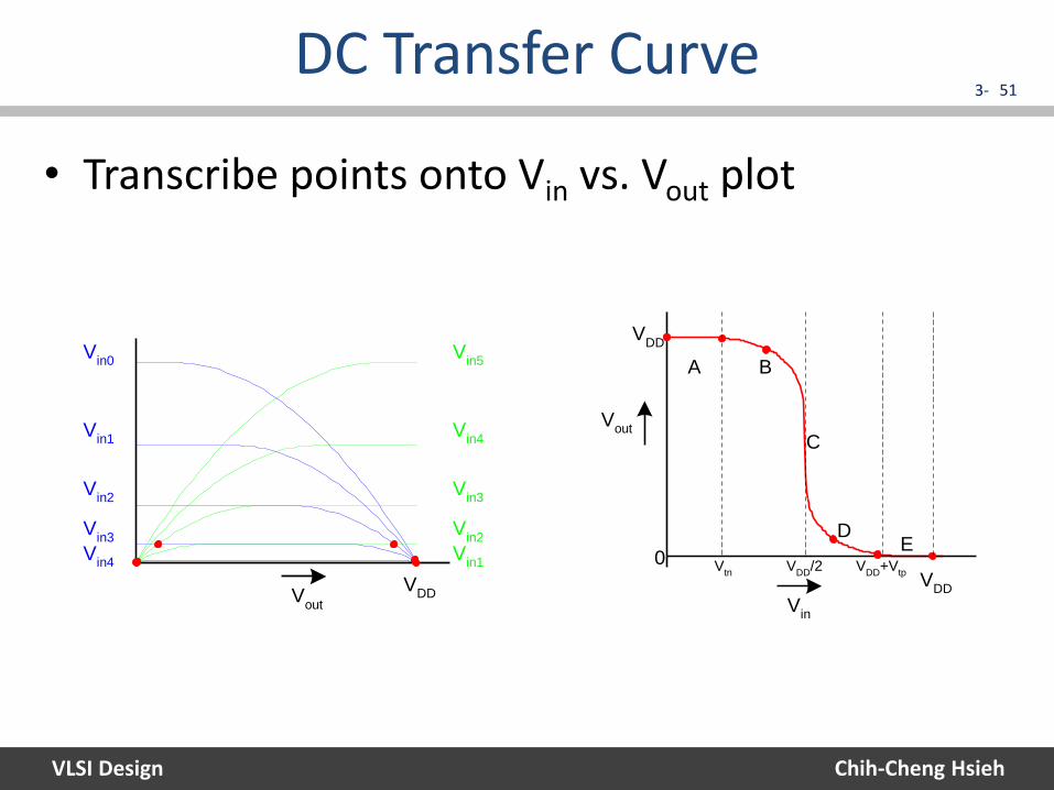
DC Transfer Curve 51
• Transcribe points onto Vin vs. Vout plot
Vin5
Vin4
Vin3
Vin2
Vin1
Vin0
Vin1
Vin2
Vin3
Vin4
Vout
VDD
CV
out
0
Vin
VDD
VDD
A B
DE
Vtn
VDD
/2 VDD
+Vtp
VLSI Design
3-
Chih-Cheng Hsieh
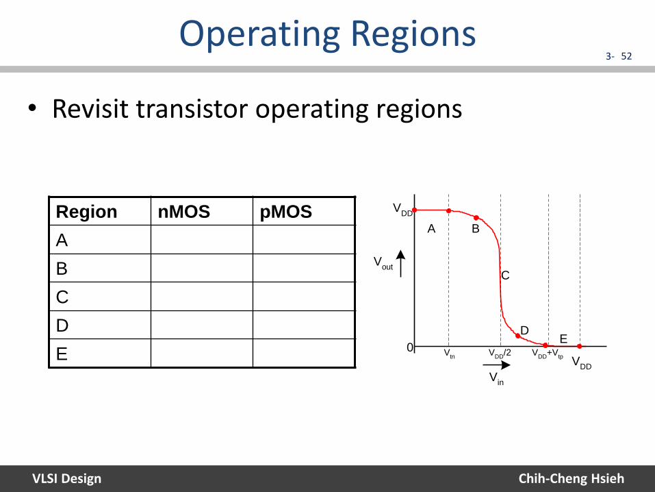
Operating Regions 52
• Revisit transistor operating regions
CV
out
0
Vin
VDD
VDD
A B
DE
Vtn
VDD
/2 VDD
+Vtp
Region nMOS pMOS
A
B
C
D
E
VLSI Design
3-
Chih-Cheng Hsieh
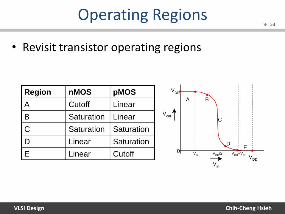
Operating Regions 53
• Revisit transistor operating regions
CV
out
0
Vin
VDD
VDD
A B
DE
Vtn
VDD
/2 VDD
+Vtp
Region nMOS pMOS
A Cutoff Linear
B Saturation Linear
C Saturation Saturation
D Linear Saturation
E Linear Cutoff
VLSI Design
3-
Chih-Cheng Hsieh
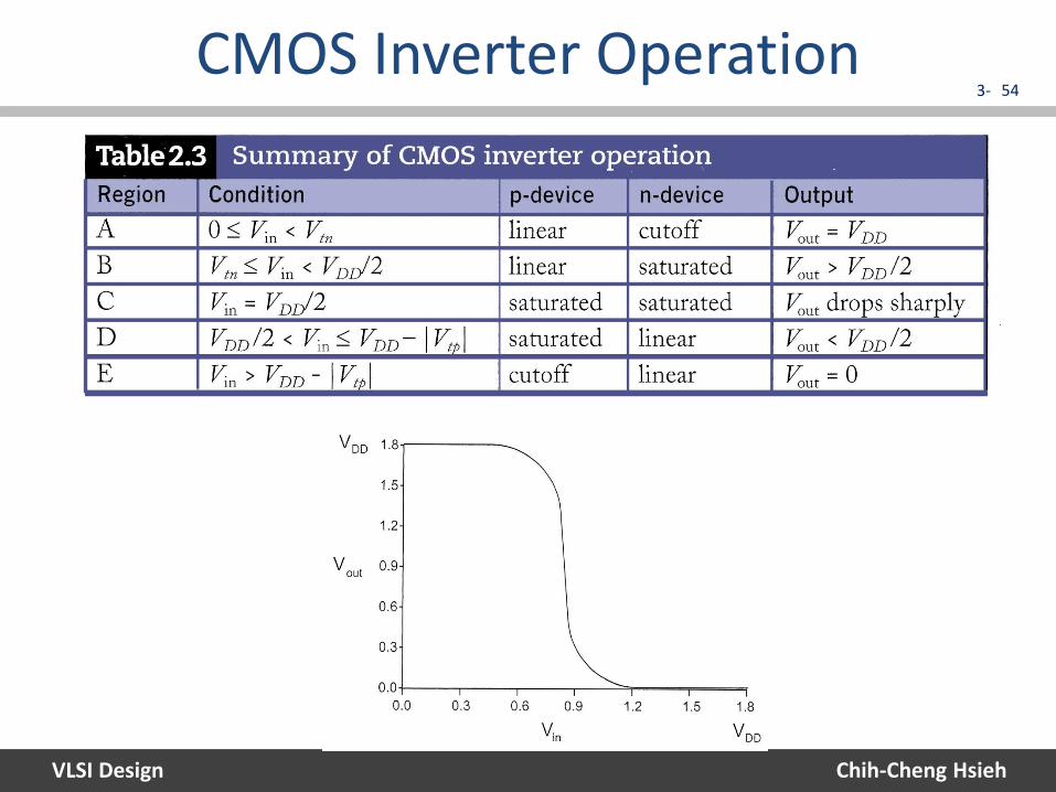
CMOS Inverter Operation 54
VLSI Design
3-
Chih-Cheng Hsieh
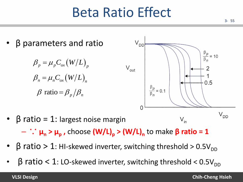
Beta Ratio Effect 55
p p ox pC W L
n n ox nC W L
• β parameters and ratio
ratio p n
• β ratio = 1: largest noise margin
– ∵ μn > μp , choose (W/L)p > (W/L)n to make β ratio = 1
• β ratio > 1: HI-skewed inverter, switching threshold > 0.5VDD
• β ratio < 1: LO-skewed inverter, switching threshold < 0.5VDD
VLSI Design
3-
Chih-Cheng Hsieh
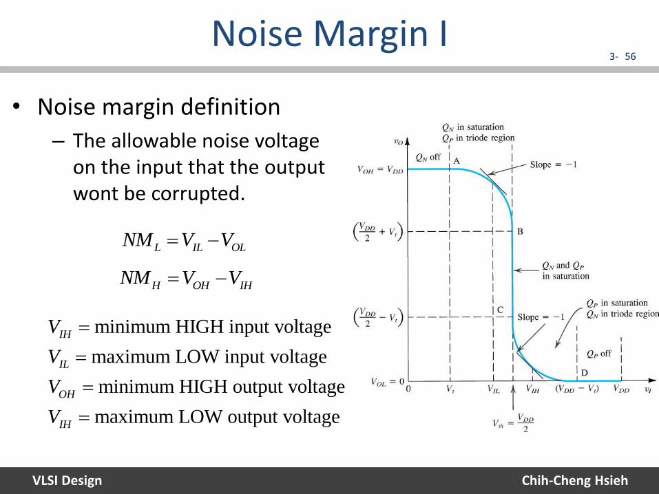
Noise Margin I 56
L IL OLNM V V
H OH IHNM V V
• Noise margin definition
– The allowable noise voltage on the input that the output wont be corrupted.
minimum HIGH input voltage
maximum LOW input voltage
minimum HIGH output voltage
maximum LOW output voltage
IH
IL
OH
IH
V
V
V
V
VLSI Design
3-
Chih-Cheng Hsieh
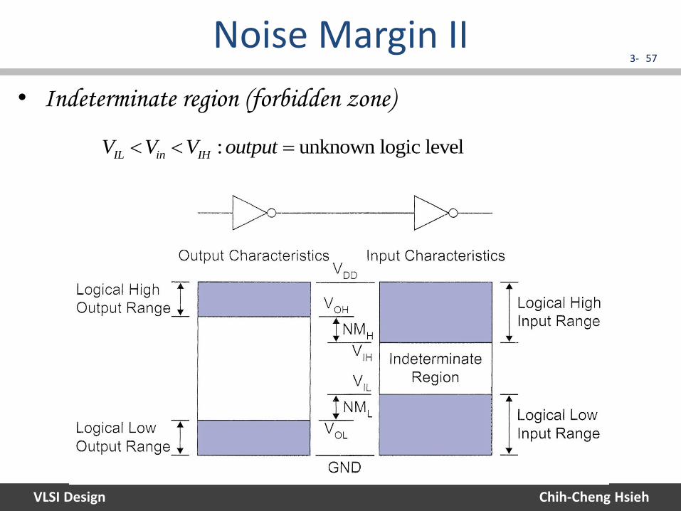
Noise Margin II 57
• Indeterminate region (forbidden zone)
: unknown logic levelIL in IHV V V output
VLSI Design
3-
Chih-Cheng Hsieh
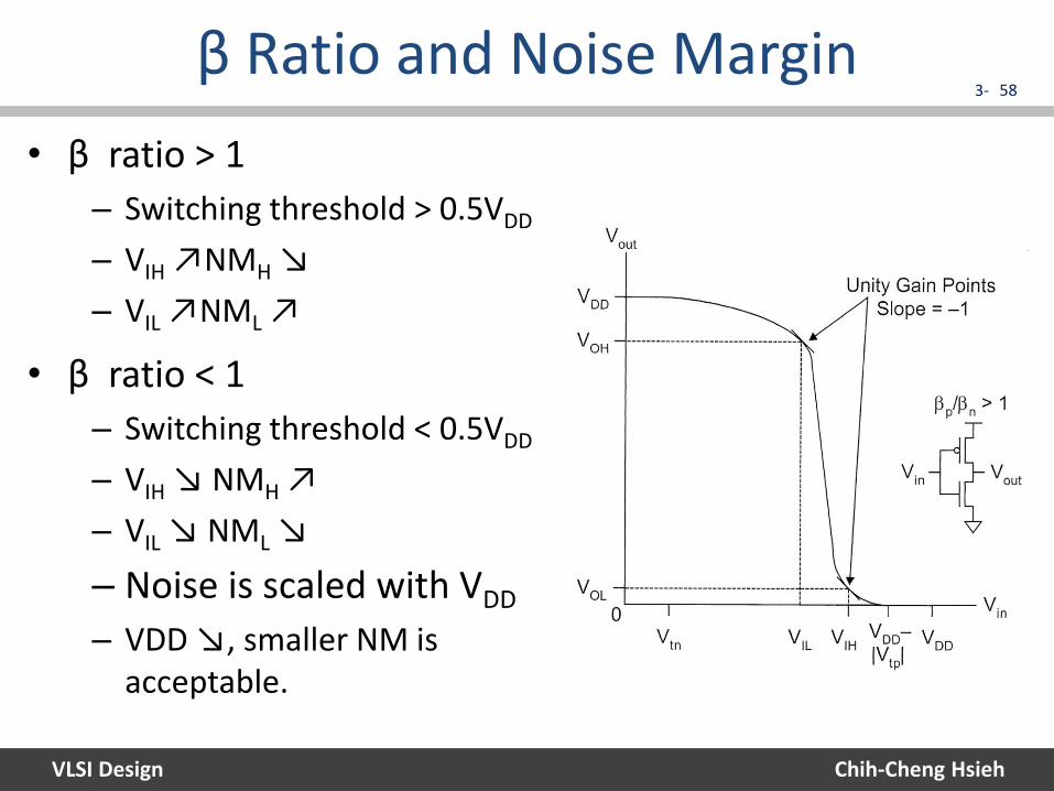
β Ratio and Noise Margin 58
• β ratio > 1
– Switching threshold > 0.5VDD
– VIH ↗NMH ↘
– VIL ↗NML ↗
• β ratio < 1
– Switching threshold < 0.5VDD
– VIH ↘ NMH ↗
– VIL ↘ NML ↘
– Noise is scaled with VDD
– VDD ↘, smaller NM is acceptable.
VLSI Design
3-
Chih-Cheng Hsieh
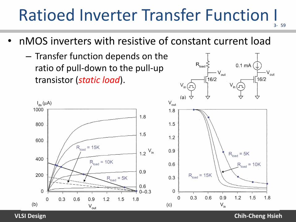
Ratioed Inverter Transfer Function I 59
• nMOS inverters with resistive of constant current load
– Transfer function depends on the ratio of pull-down to the pull-up transistor (static load).
VLSI Design
3-
Chih-Cheng Hsieh
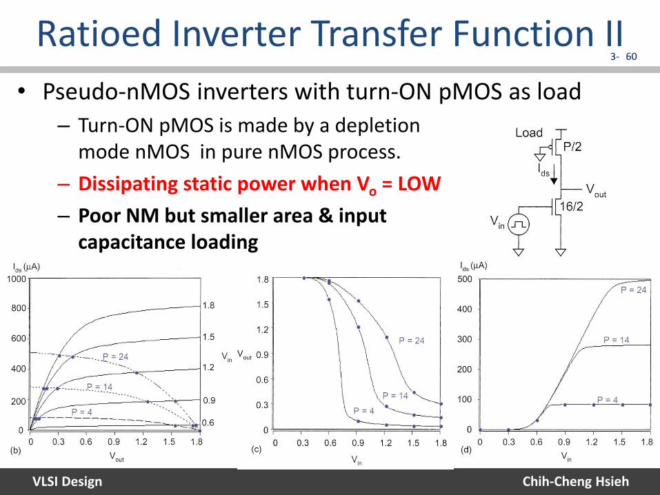
Ratioed Inverter Transfer Function II 60
• Pseudo-nMOS inverters with turn-ON pMOS as load
– Turn-ON pMOS is made by a depletion mode nMOS in pure nMOS process.
– Dissipating static power when Vo = LOW
– Poor NM but smaller area & input capacitance loading
VLSI Design
3-
Chih-Cheng Hsieh
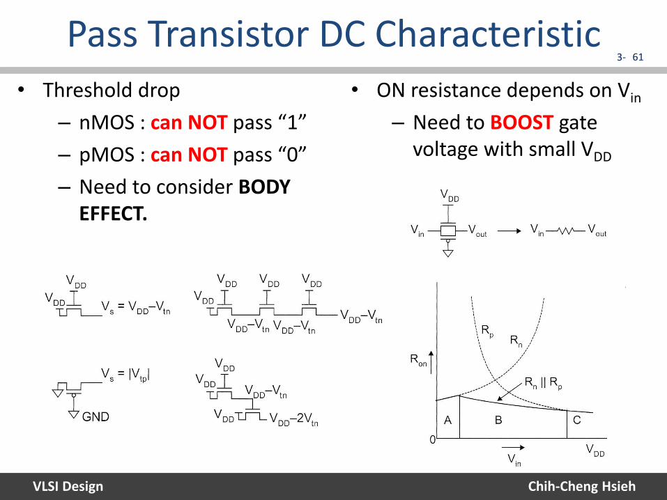
Pass Transistor DC Characteristic 61
• Threshold drop
– nMOS : can NOT pass “1”
– pMOS : can NOT pass “0”
– Need to consider BODY EFFECT.
• ON resistance depends on Vin
– Need to BOOST gate voltage with small VDD
VLSI Design
3-
Chih-Cheng Hsieh
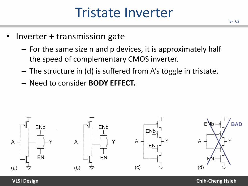
Tristate Inverter 62
• Inverter + transmission gate
– For the same size n and p devices, it is approximately half the speed of complementary CMOS inverter.
– The structure in (d) is suffered from A’s toggle in tristate.
– Need to consider BODY EFFECT.
VLSI Design
3-
Chih-Cheng Hsieh
63
1. Introduction
2. Ideal I-V Characteristics
3. Nonideal I-V Effects
4. C-V Characteristics
5. DC Transfer Characteristics
6. Switch-level RC Delay Models
Outline
VLSI Design
3-
Chih-Cheng Hsieh
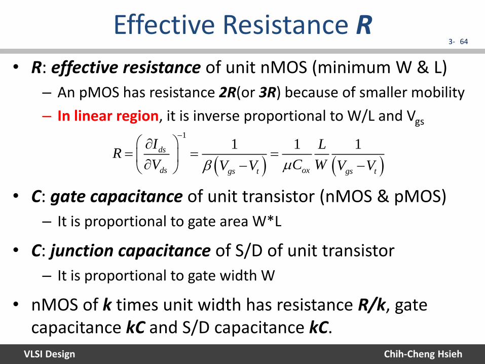
Effective Resistance R 64
• R: effective resistance of unit nMOS (minimum W & L)
– An pMOS has resistance 2R(or 3R) because of smaller mobility
– In linear region, it is inverse proportional to W/L and Vgs
1
1 1 1ds
ds oxgs t gs t
I LR
V C WV V V V
• C: gate capacitance of unit transistor (nMOS & pMOS)
– It is proportional to gate area W*L
• C: junction capacitance of S/D of unit transistor
– It is proportional to gate width W
• nMOS of k times unit width has resistance R/k, gate capacitance kC and S/D capacitance kC.
VLSI Design
3-
Chih-Cheng Hsieh
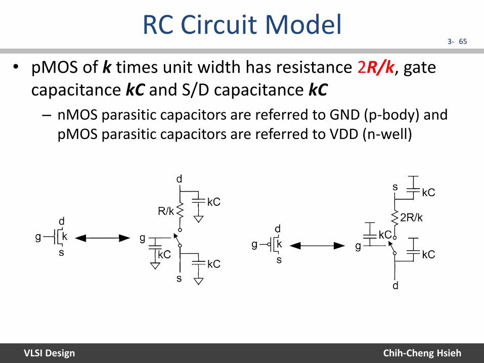
RC Circuit Model 65
• pMOS of k times unit width has resistance 2R/k, gate capacitance kC and S/D capacitance kC
– nMOS parasitic capacitors are referred to GND (p-body) and pMOS parasitic capacitors are referred to VDD (n-well)
VLSI Design
3-
Chih-Cheng Hsieh
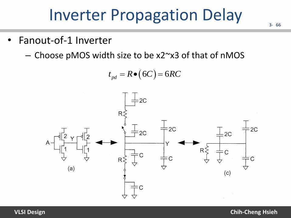
Inverter Propagation Delay 66
• Fanout-of-1 Inverter
– Choose pMOS width size to be x2~x3 of that of nMOS
6 6pdt R C RC
VLSI Design
3-
Chih-Cheng Hsieh
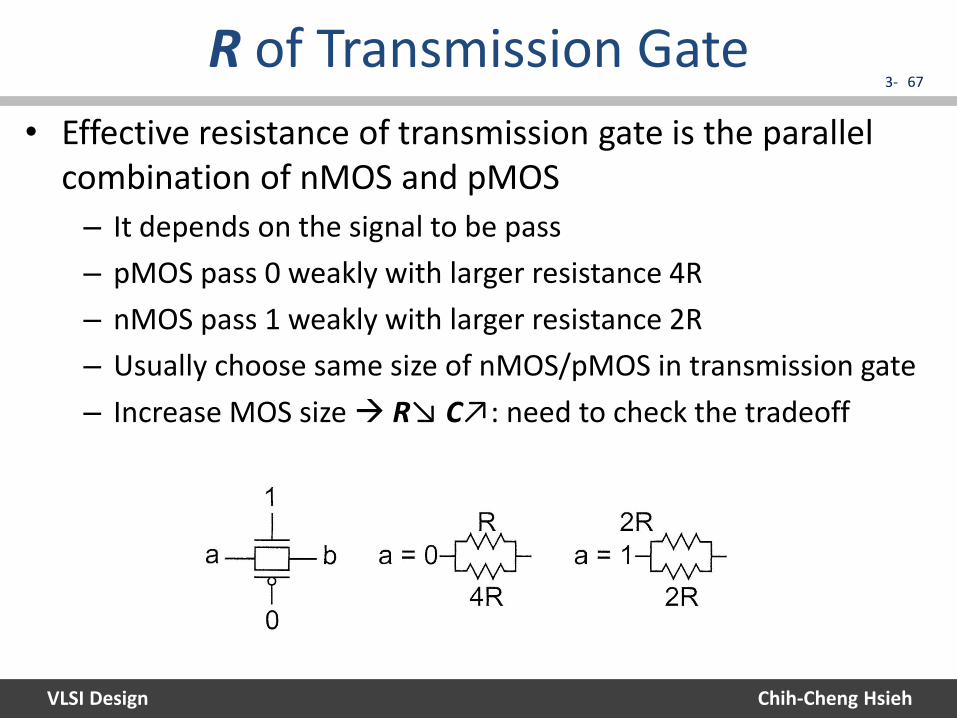
R of Transmission Gate 67
• Effective resistance of transmission gate is the parallel combination of nMOS and pMOS
– It depends on the signal to be pass
– pMOS pass 0 weakly with larger resistance 4R
– nMOS pass 1 weakly with larger resistance 2R
– Usually choose same size of nMOS/pMOS in transmission gate
– Increase MOS size R↘ C↗: need to check the tradeoff