Embed Size (px)
Citation preview
1
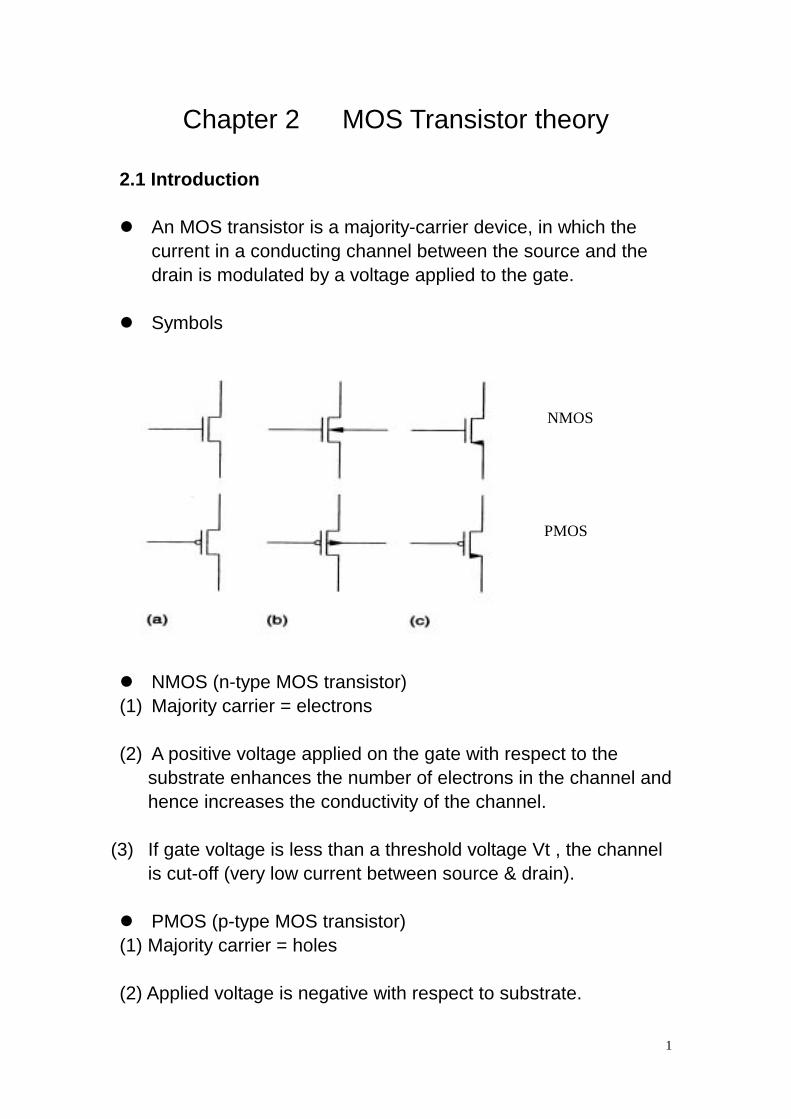
Chapter 2 MOS Transistor theory 2.1 Introduction An MOS transistor is a majority-carrier device, in which the
current in a conducting channel between the source and the drain is modulated by a voltage applied to the gate.
Symbols
NMOS (n-type MOS transistor)
(1) Majority carrier = electrons (2) A positive voltage applied on the gate with respect to the
substrate enhances the number of electrons in the channel and hence increases the conductivity of the channel.
(3) If gate voltage is less than a threshold voltage Vt , the channel
is cut-off (very low current between source & drain). PMOS (p-type MOS transistor)
(1) Majority carrier = holes (2) Applied voltage is negative with respect to substrate.
NMOS
PMOS
2
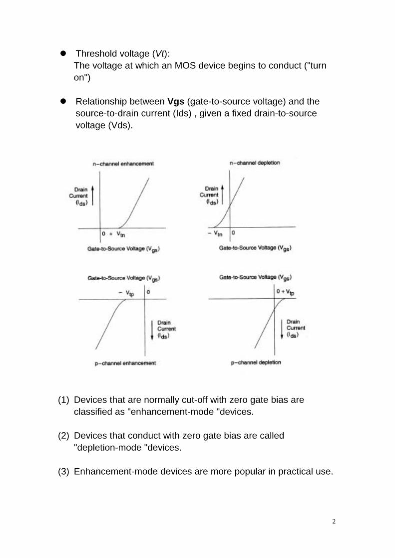
Threshold voltage (Vt): The voltage at which an MOS device begins to conduct ("turn on") Relationship between Vgs (gate-to-source voltage) and the
source-to-drain current (Ids) , given a fixed drain-to-source voltage (Vds).
(1) Devices that are normally cut-off with zero gate bias are
classified as "enhancement-mode "devices. (2) Devices that conduct with zero gate bias are called
"depletion-mode "devices.
(3) Enhancement-mode devices are more popular in practical use.
3
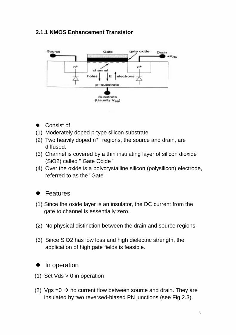
2.1.1 NMOS Enhancement Transistor Consist of
(1) Moderately doped p-type silicon substrate (2) Two heavily doped n + regions, the source and drain, are
diffused. (3) Channel is covered by a thin insulating layer of silicon dioxide
(SiO2) called " Gate Oxide " (4) Over the oxide is a polycrystalline silicon (polysilicon) electrode,
referred to as the "Gate"
Features (1) Since the oxide layer is an insulator, the DC current from the
gate to channel is essentially zero. (2) No physical distinction between the drain and source regions. (3) Since SiO2 has low loss and high dielectric strength, the
application of high gate fields is feasible.
In operation (1) Set Vds > 0 in operation (2) Vgs =0 no current flow between source and drain. They are
insulated by two reversed-biased PN junctions (see Fig 2.3).
4
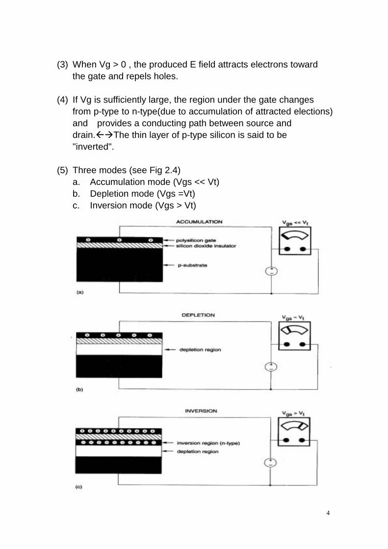
(3) When Vg > 0 , the produced E field attracts electrons toward
the gate and repels holes. (4) If Vg is sufficiently large, the region under the gate changes
from p-type to n-type(due to accumulation of attracted elections) and provides a conducting path between source and drain. The thin layer of p-type silicon is said to be "inverted".
(5) Three modes (see Fig 2.4)
a. Accumulation mode (Vgs << Vt) b. Depletion mode (Vgs =Vt) c. Inversion mode (Vgs > Vt)
5
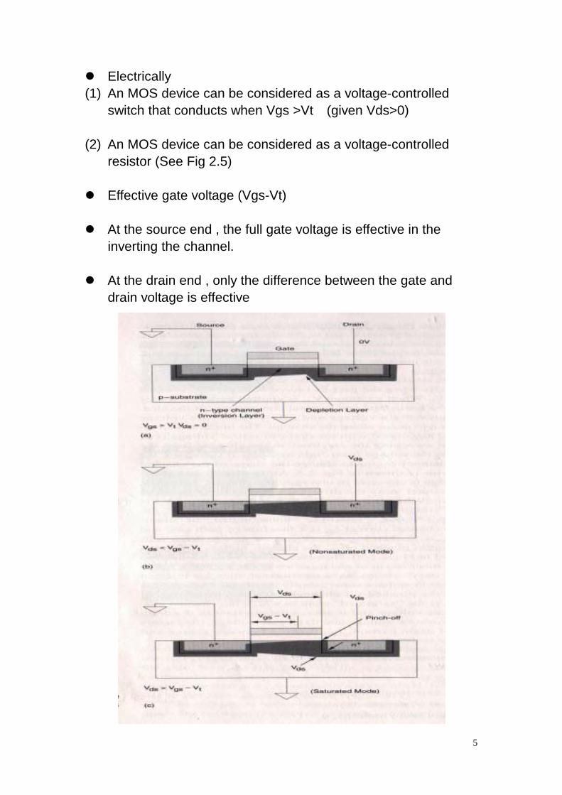
Electrically (1) An MOS device can be considered as a voltage-controlled
switch that conducts when Vgs >Vt (given Vds>0) (2) An MOS device can be considered as a voltage-controlled
resistor (See Fig 2.5) Effective gate voltage (Vgs-Vt)
At the source end , the full gate voltage is effective in the
inverting the channel. At the drain end , only the difference between the gate and
drain voltage is effective
6
Pinch-off (1) Vds > Vgs-Vt => Vgd < Vt => Vd > Vg –Vt (Vg is not big
enough) (2) The channel no longer reaches the drain. (Fig 2.5 c) (3) As electrons leave the drain depletion region and are
subsequently accelerated toward the drain. (4) The voltage across the pinched-off region remains at (Vgs-Vt)
=>”saturated” state in which the channel current as controlled by Vg , and is independent of Vd
For fixed Vds and Vg , Ids is function of
(1) Distance between drain & source (2) Channel width (3) Vt (4) Thickness of gate oxide (5) The dielectric constant of gate oxide
(6) Carrier (hole or electron) mobility , μ.
Conducting mode
(1) ”cut-off ” region : Ids ≈ 0 , Vgs < Vt (2) ” Nonsaturated” region : weak inversion region, when Ids
depends on Vg & Vd (3) ”Saturated“ region: channel is strongly inverted and Ids is
ideally independent of Vds (pinch-off region) (4) ”Avalanche breakdown” (pinch-through) : very high Vd => gate
has no control over Ids
7
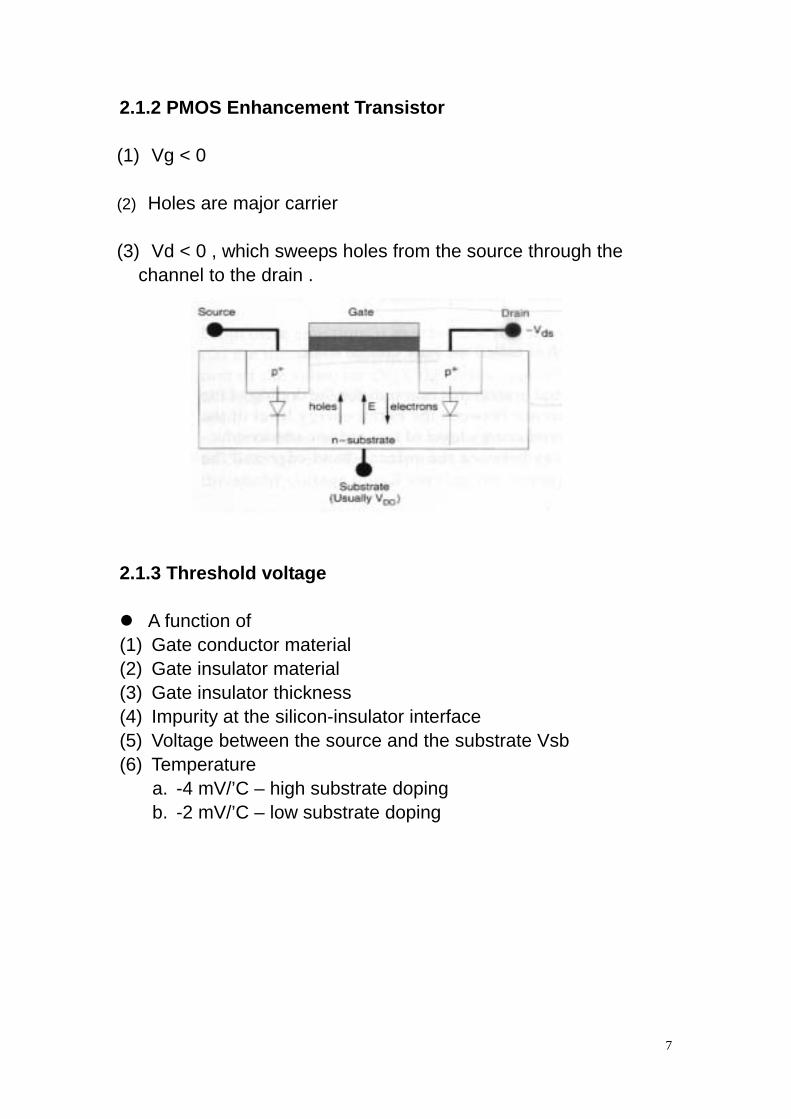
2.1.2 PMOS Enhancement Transistor (1) Vg < 0 (2) Holes are major carrier (3) Vd < 0 , which sweeps holes from the source through the
channel to the drain .
2.1.3 Threshold voltage A function of
(1) Gate conductor material (2) Gate insulator material (3) Gate insulator thickness (4) Impurity at the silicon-insulator interface (5) Voltage between the source and the substrate Vsb (6) Temperature
a. -4 mV/’C – high substrate doping b. -2 mV/’C – low substrate doping
8
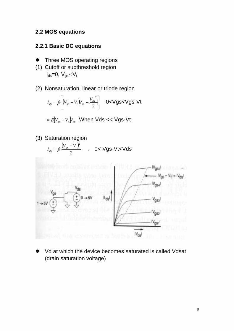
2.2 MOS equations 2.2.1 Basic DC equations Three MOS operating regions
(1) Cutoff or subthreshold region Ids=0, Vgs≤Vt
(2) Nonsaturation, linear or triode region
( )
−−=
2
2ds
dstgsdsVVVVI β 0<Vgs<Vgs-Vt
[ ] dstgs VVV −≈ β When Vds << Vgs-Vt
(3) Saturation region
( )2
2tgs
ds
VVI
−= β , 0< Vgs-Vt<Vds
Vd at which the device becomes saturated is called Vdsat
(drain saturation voltage)
9
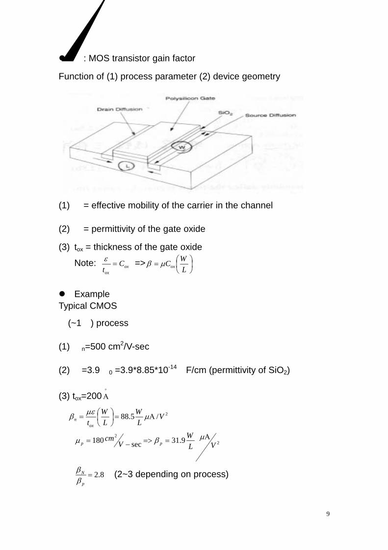
β: MOS transistor gain factor
Function of (1) process parameter (2) device geometry
(1) μ= effective mobility of the carrier in the channel
(2) ε= permittivity of the gate oxide
(3) tox = thickness of the gate oxide
Note: oxox
Ct
=ε =>
=
LWCoxµβ
Example
Typical CMOS
◎ (~1μ) process
(1) μn=500 cm2/V-sec
(2) ε=3.9ε0 =3.9*8.85*10-14 F/cm (permittivity of SiO2)
(3) tox=200°
Α
2/5.88 VLW
LW
toxn Α=
= µµεβ
◎ 22
9.31sec180 VLW
Vcm
ppΑ==>−= µβµ
◎ 8.2=p
N
ββ (2~3 depending on process)
10
2.2.2. Seven Second-order Effect SPICE : Simulation Program with Integrated Circuit Emphasis
LEVEL: 1,2,3
(1) Basic DC Equations + Some second-order effects (2) Based on device physics (3) Add more parameters to match real circuits
e.g., Process gain factor
SPICE : Kp (10-100 μA/V2 with 10%-20% variation)
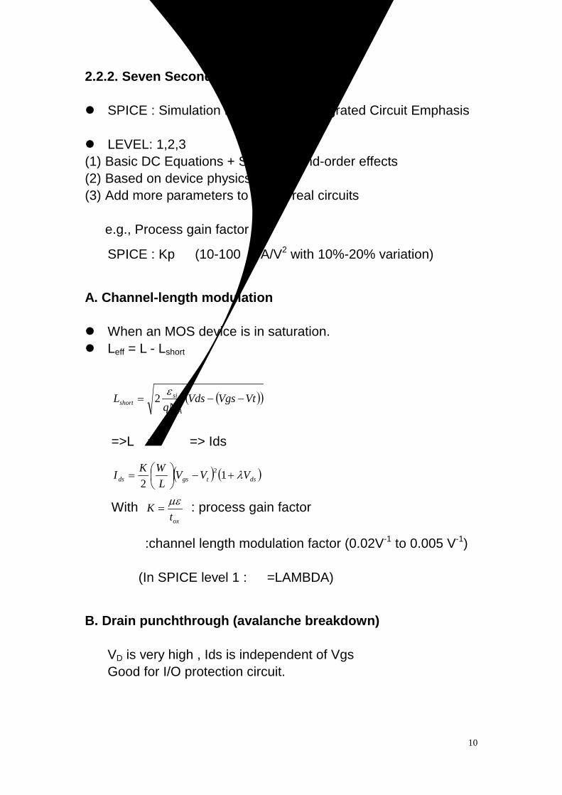
A. Channel-length modulation When an MOS device is in saturation. Leff = L - Lshort
( )( )VtVgsVdsqN
LA
sishort −−=
ε2
=>L↓=>β↑=> Ids↑
( ) ( )dstgsds VVVLWKI λ+−
= 1
22
With oxt
K µε= : process gain factor
λ:channel length modulation factor (0.02V-1 to 0.005 V-1)
(In SPICE level 1 : λ=LAMBDA)
B. Drain punchthrough (avalanche breakdown)
VD is very high , Ids is independent of Vgs Good for I/O protection circuit.
11
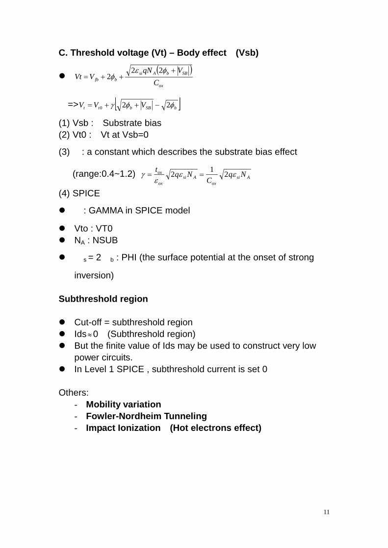
C. Threshold voltage (Vt) – Body effect (Vsb)
( )ox
SBbAsibfb C
VqNVVt
+++=
φεφ
222
=> [ ]bSBbtt VVV φφγ 220 −++=
(1) Vsb : Substrate bias (2) Vt0 : Vt at Vsb=0
(3) γ: a constant which describes the substrate bias effect
(range:0.4~1.2) Asiox
Asiox
ox NqC
Nqt εεε
γ 212 ==
(4) SPICE
γ: GAMMA in SPICE model
Vto : VT0 NA : NSUB
ψs = 2ψb : PHI (the surface potential at the onset of strong
inversion) Subthreshold region Cut-off = subthreshold region Ids≈0 (Subthreshold region) But the finite value of Ids may be used to construct very low
power circuits. In Level 1 SPICE , subthreshold current is set 0
Others:
- Mobility variation - Fowler-Nordheim Tunneling - Impact Ionization (Hot electrons effect)
12
2.2.3 MOS Models MOS model = Ideal Equations + Second-order Effects +
Additional Curve-fitting parameters Many semiconductor vendors expend a lot of effects to model
the devices they manufacture.(Standard : Level 3 SPICE)
Main SPICE DC parameters in level 1,2,3 in 1μn-well CMOS
process.
13
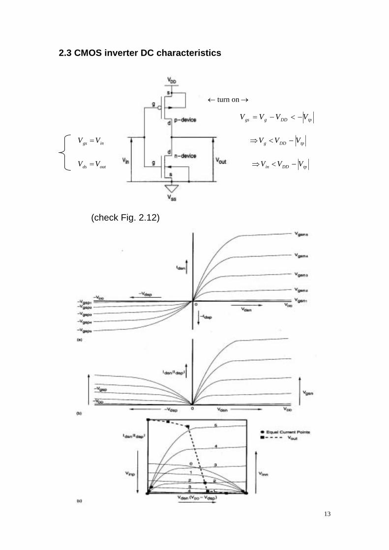
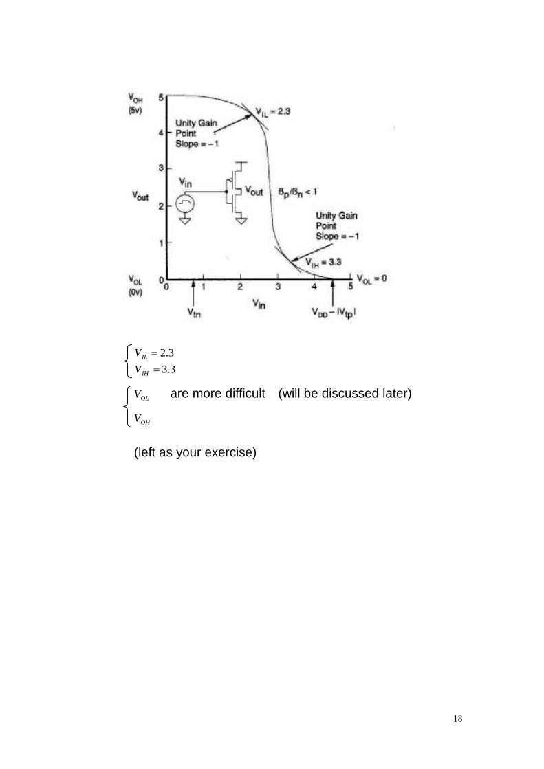
2.3 CMOS inverter DC characteristics →← onturn
tpDDggs VVVV −<−=
ings VV = tpDDg VVV −<⇒
outds VV = tpDDin VVV −<⇒
(check Fig. 2.12)
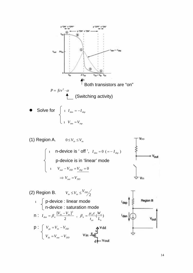
14
Both transistors are “on” α⋅= 2fcvP (Switching activity)
Solve for dspdsn II −=
inpinn VV =
(1) Region A. tnin VV ≤≤0
n-device is ‘ off ’, ) ( 0 dspdsn II −==
p-device is in ‘linear’ mode 0==− dspDDout VVV
DDout VV =⇒
(2) Region B. 2DD
intnVVV ≤≤
p-device : linear mode n-device : saturation mode
n : )( , 2
][ 2
n
n
ox
nn
tninndsn L
Wt
VVI
εµββ =
−=
p : DDings VVV −=
DDoutds VVV −=
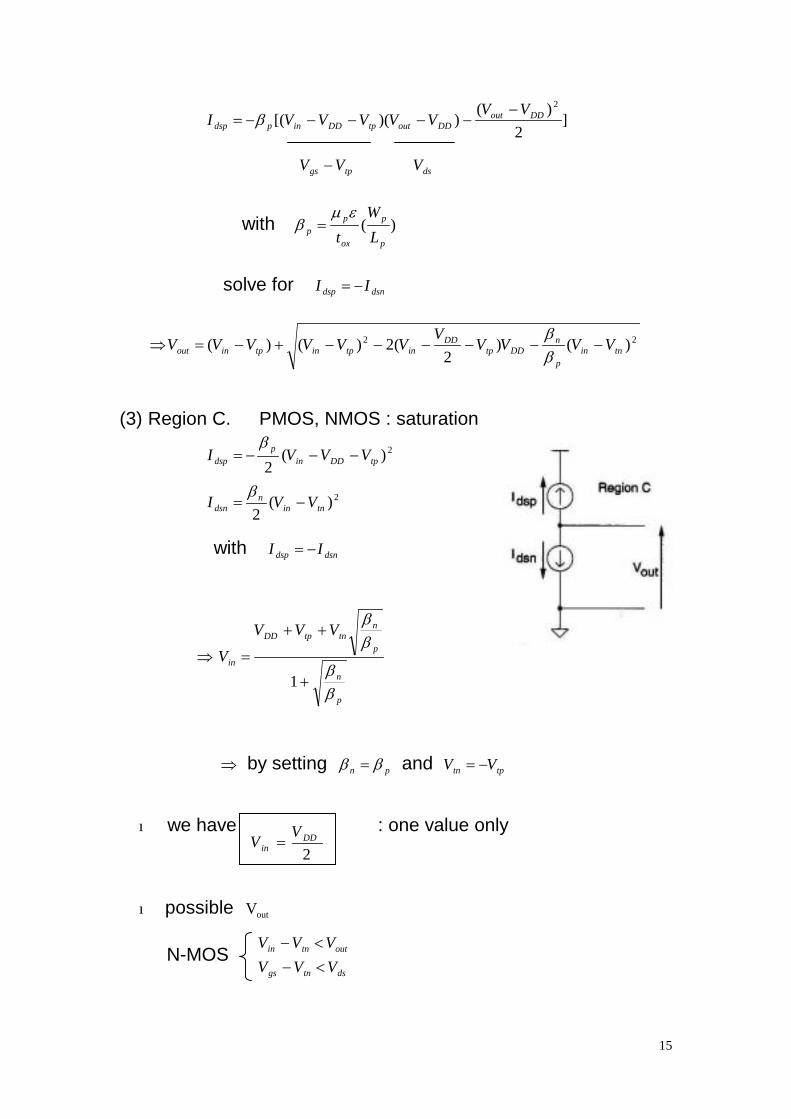
15
∴ ]2
)())([(
2DDout
DDouttpDDinpdspVV
VVVVVI−
−−−−−= β
tpgs VV − dsV
with )( p
p
ox
pp L
Wtεµ
β =
solve for dsndsp II −=
22 )()2
(2)()( tninp
nDDtp
DDintpintpinout VVVV
VVVVVVV −−−−−−+−=⇒
ββ
(3) Region C. PMOS, NMOS : saturation
2)(2 tpDDin
pdsp VVVI −−−=
β
2)(2 tnin
ndsn VVI −=
β
with dsndsp II −=
p
n
p
ntntpDD
in
VVV
V
ββ
ββ
+
++
=⇒
1
⇒ by setting pn ββ = and tptn VV −=
we have : one value only
possible outV
N-MOS dstngs
outtnin
VVVVVV
<−<−
2DD
inVV =
16
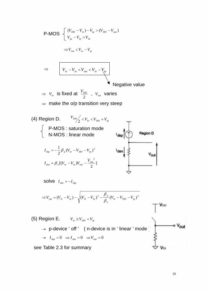
P-MOS dstpgs
outDDtpinDD
VVVVVVVV
>−
−>−− )()(
tpinout VVV −<⇒
⇒ ☆
Negative value
⇒ inV is fixed at 2DDV , outV varies
⇒ make the o/p transition very steep
(4) Region D. tpDDinDD VVVV +<<2
P-MOS : saturation mode N-MOS : linear mode
2)(21
tpDDinpdsp VVVI −−−= β
]2
)[(2
outouttninndsn
VVVVI −−= β
solve dspdsn II −=
22 )()()( tpDDinn
ptnintninout VVVVVVVV −−−−−−=⇒
ββ
(5) Region E. tpDDin VVV +≥
→ p-device ‘ off ‘ ( n-device is in ‘ linear ’ mode )
→ 0=dspI 0 =⇒ dsnI 0 =⇒ outV
see Table 2.3 for summary
tpinouttnin VVVVV −<<−
17
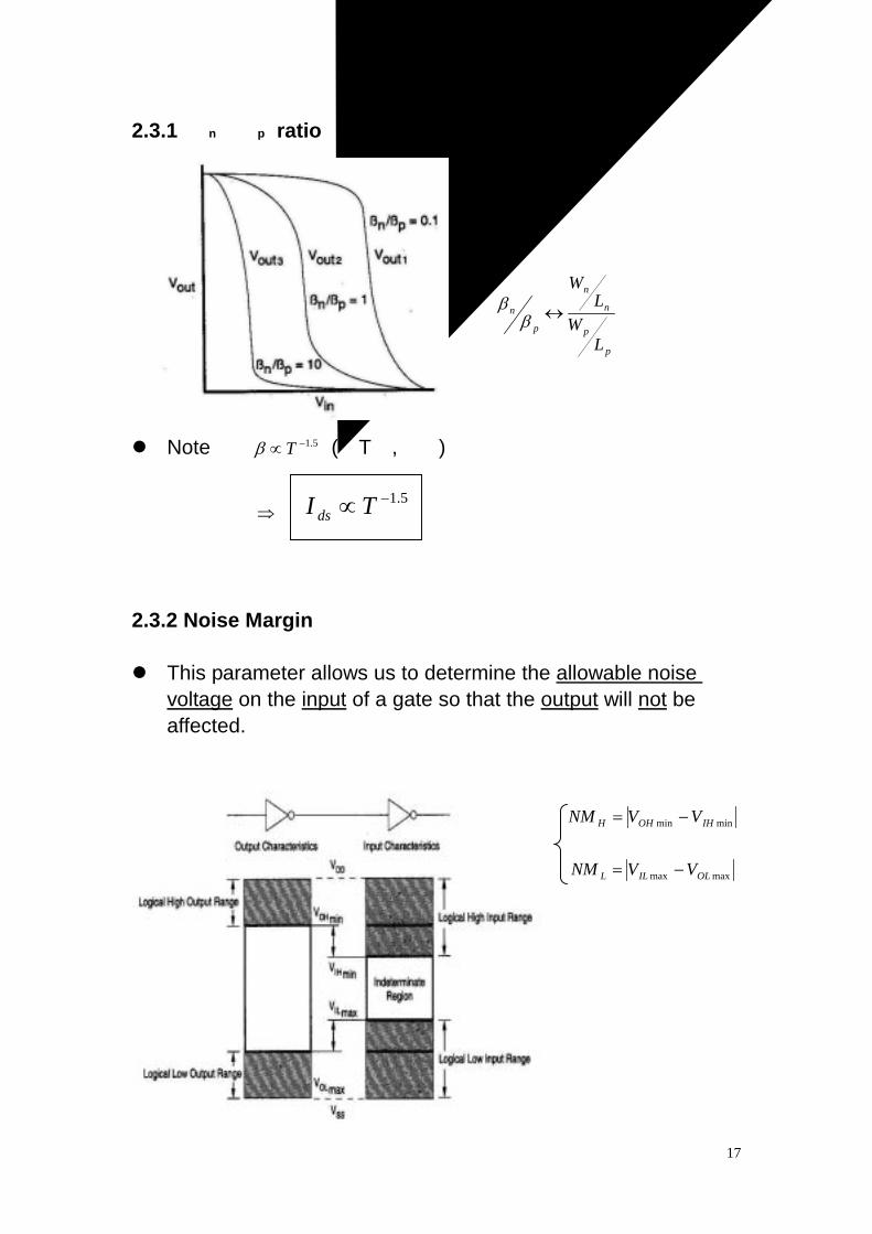
2.3.1 βn/βp ratio ( watch Eq.(2.24) )
p
p
n
n
p
n
LW
LW
↔ββ
Note 5.1−∝Tβ (∵T↑,μ↓)
⇒
2.3.2 Noise Margin This parameter allows us to determine the allowable noise
voltage on the input of a gate so that the output will not be affected.
minmin IHOHH VVNM −=
maxmax OLILL VVNM −=
How to determine LH NMNM &
5.1−∝TI ds
18
3.2=ILV 3.3=IHV
OLV are more difficult (will be discussed later)
OHV (left as your exercise)
19
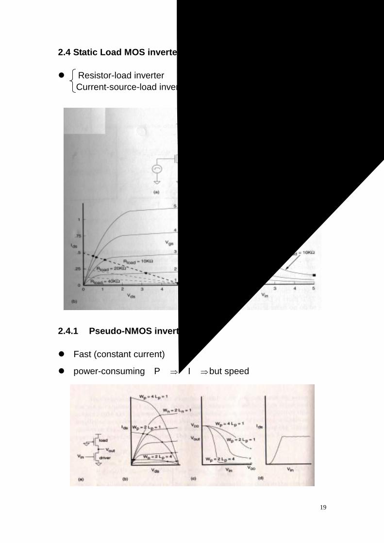
2.4 Static Load MOS inverters Resistor-load inverter
Current-source-load inverter
2.4.1 Pseudo-NMOS inverter Fast (constant current)
power-consuming P↑⇒∵I↑⇒but speed↑
20
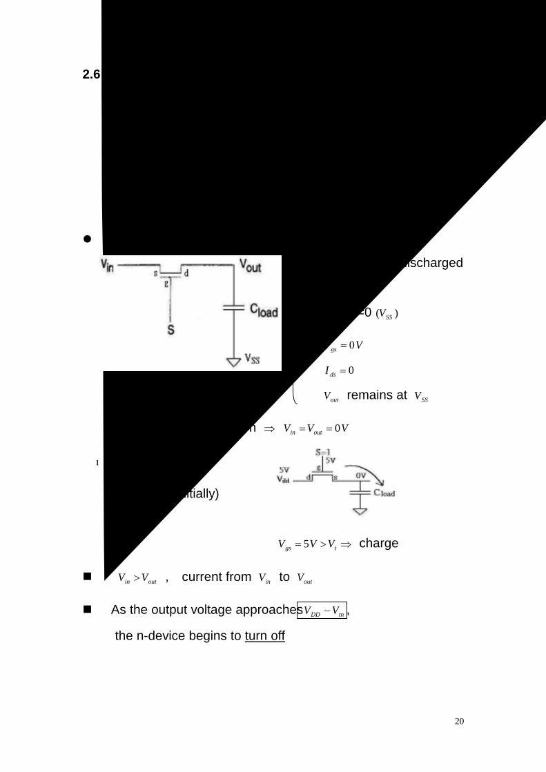
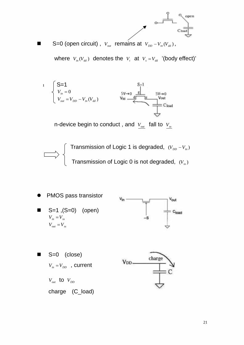
2.6 The Transmission Gate (PMOS)
(NMOS)
NMOS pass transistor
loadC is initially discharged
SSout VV =
with S=0 )( SSV
VVgs 0=
0=dsI
outV remains at SSV
tgs VVV >= 5 , NMOS On ⇒ VVV outin 0==
S=1 )( ddV
DDgs VV = (initially)
⇒>= tgs VVV 5 charge
∵ outin VV > , current from inV to outV
As the output voltage approaches tnDD VV − ,
the n-device begins to turn off
21
S=0 (open circuit) , outV remains at )( ddtnDD VVV − ,
where )( ddtn VV denotes the tV at dds VV = ’(body effect)’
S=1 0=inV )( ddtnDDout VVVV −=
n-device begin to conduct , and outV fall to ssV
Transmission of Logic 1 is degraded, )( tnDD VV −
Transmission of Logic 0 is not degraded, )( ssV
PMOS pass transistor
S=1 ,(S=0) (open)
ssin VV = ssout VV = S=0 (close)
DDin VV = , current
outV to DDV
charge (C_load)
22
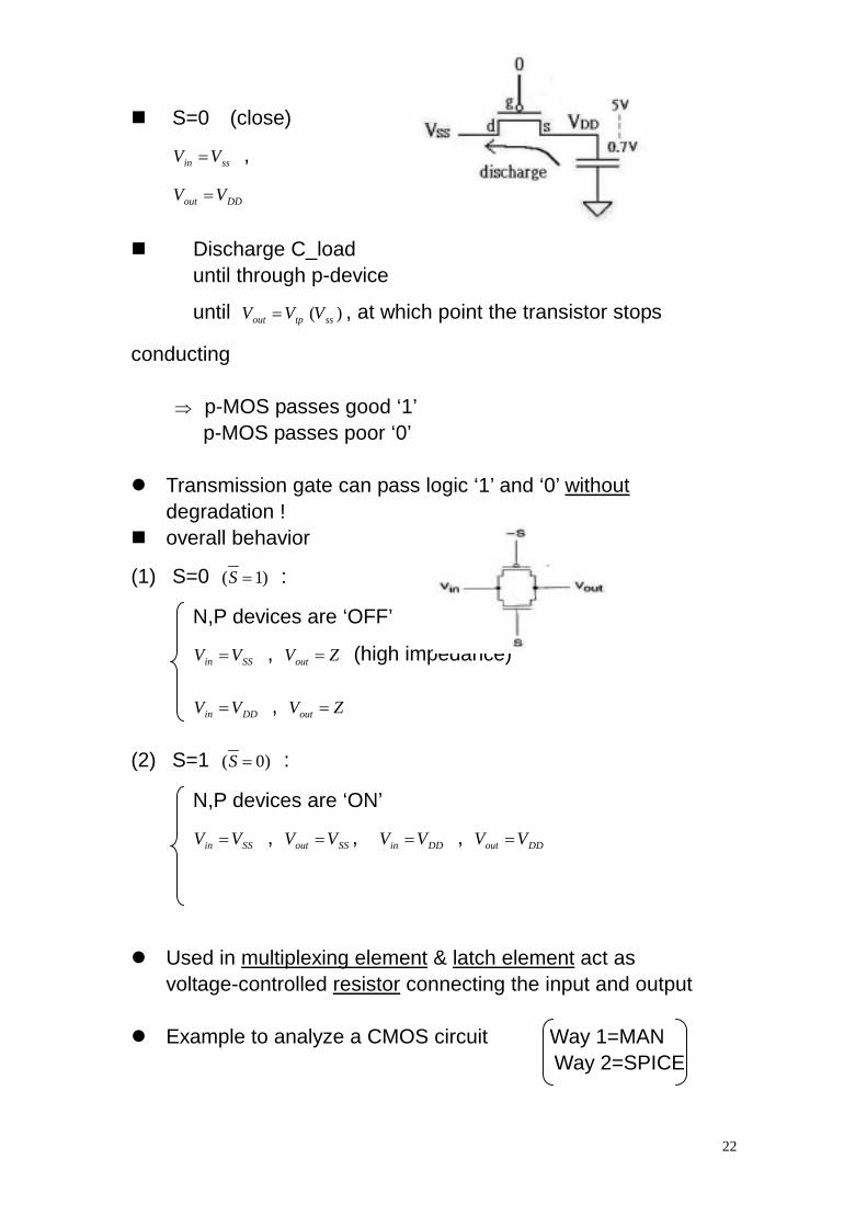
S=0 (close)
ssin VV = ,
DDout VV = Discharge C_load
until through p-device
until )( sstpout VVV = , at which point the transistor stops
conducting ⇒ p-MOS passes good ‘1’ p-MOS passes poor ‘0’ Transmission gate can pass logic ‘1’ and ‘0’ without
degradation ! overall behavior
(1) S=0 )1( =S :
N,P devices are ‘OFF’
SSin VV = , ZVout = (high impedance)
DDin VV = , ZVout =
(2) S=1 )0( =S :
N,P devices are ‘ON’
SSin VV = , SSout VV = , DDin VV = , DDout VV =
Used in multiplexing element & latch element act as
voltage-controlled resistor connecting the input and output Example to analyze a CMOS circuit Way 1=MAN
Way 2=SPICE
23
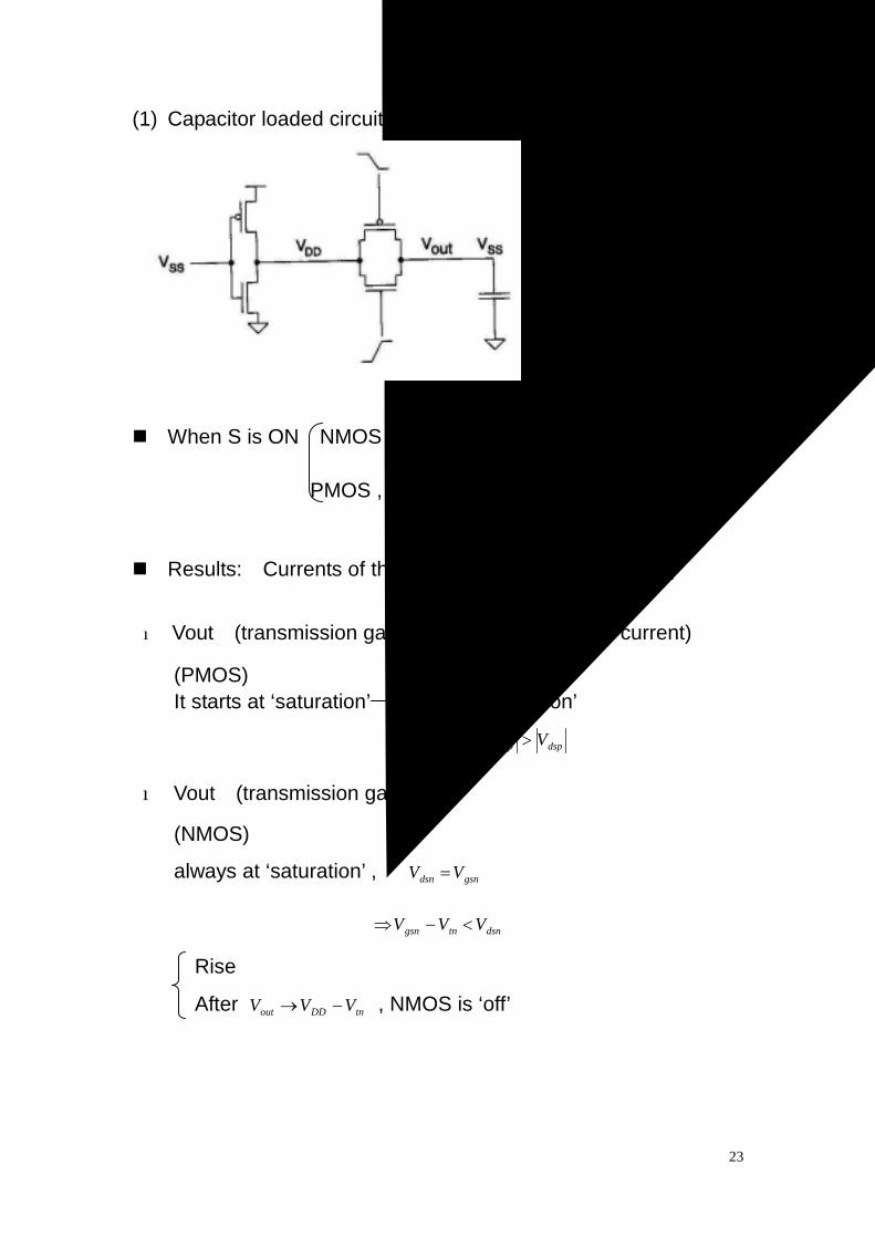
(1) Capacitor loaded circuit Cload at Vss * Cload is large When S is ON NMOS , S = 0 1
PMOS , S = 1 0
Results: Currents of the pass transistor are monitored
Vout↑(transmission gate) , 5)( −=pVgs (constant current)
(PMOS) It starts at ‘saturation’ ‘nonsaturation’
as dsptpgsp VVV >−
Vout↑(transmission gate)
(NMOS)
always at ‘saturation’ , ∵ gsndsn VV =
dsntngsn VVV <−⇒
Rise
After tnDDout VVV −→ , NMOS is ‘off’
24
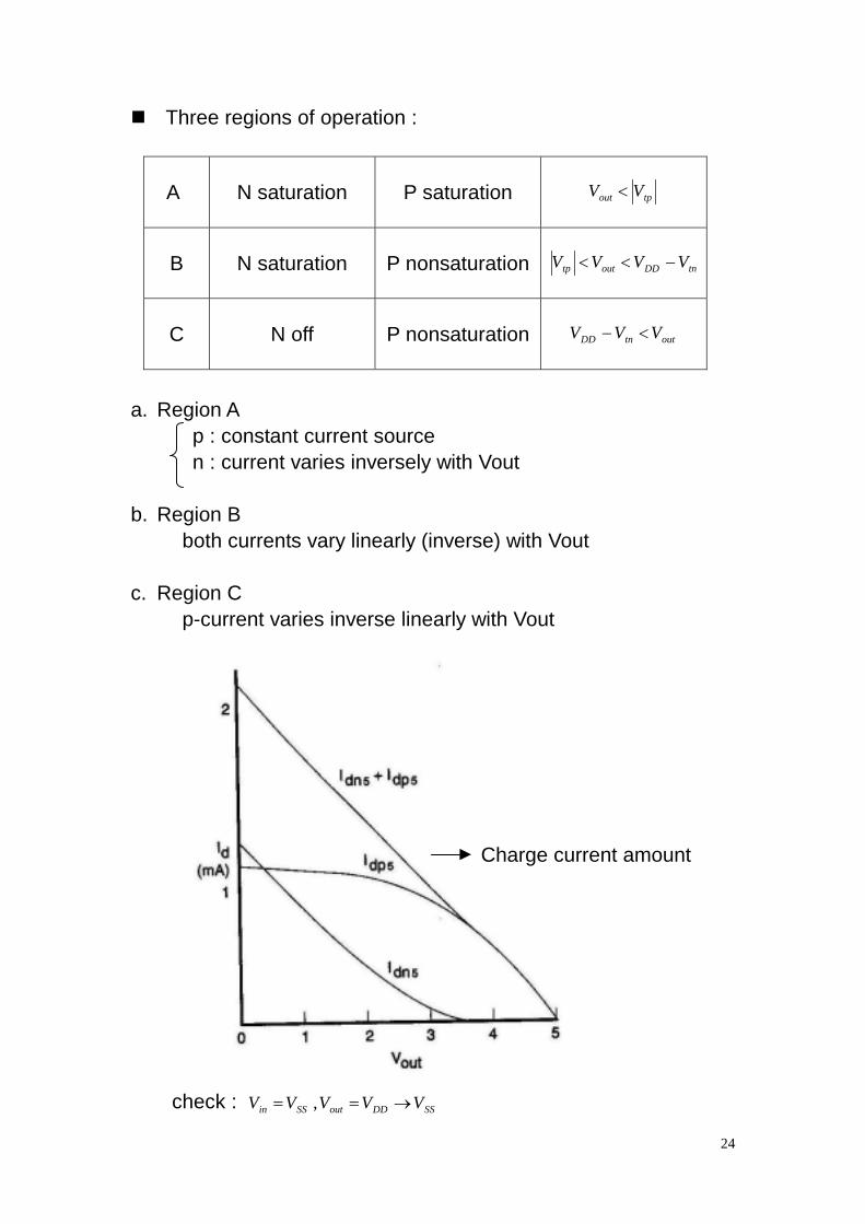
Three regions of operation :
A
N saturation P saturation tpout VV <
B
N saturation P nonsaturation tnDDouttp VVVV −<<
C
N off P nonsaturation outtnDD VVV <−
a. Region A p : constant current source n : current varies inversely with Vout b. Region B both currents vary linearly (inverse) with Vout c. Region C p-current varies inverse linearly with Vout Charge current amount
check : SSDDoutSSin VVVVV →== ,
25
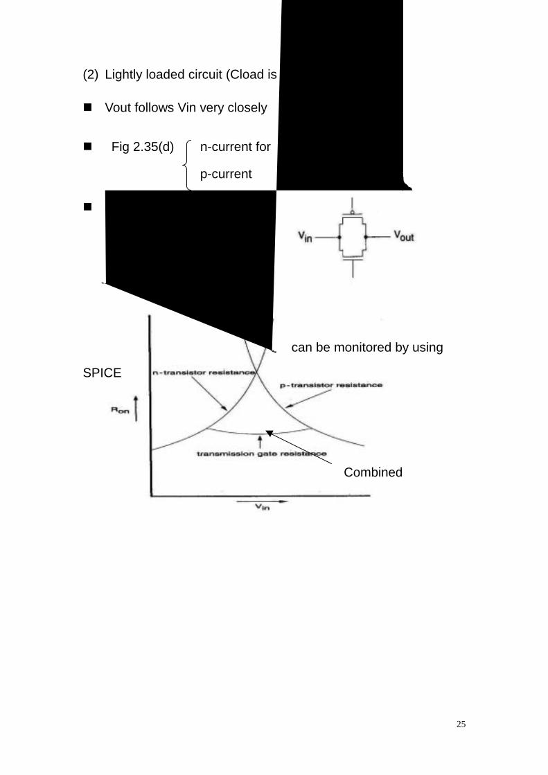
(2) Lightly loaded circuit (Cload is small) Vout follows Vin very closely
Fig 2.35(d) n-current for 1.0−=− inout VV
p-current Three regions of operation :
a. n (linear) , p (off) b. n (linear) , p (linear) c. n (off) , p (linear)
← can be monitored by using
SPICE Combined