Embed Size (px)
Citation preview

國立交通大學
電子工程學系 電子研究所
碩士論文
藉由更改電路佈局來增加聚焦離子束對訊號的探測能
力與修正電路之能力
Design-for-Debug Layout Adjustment for FIB Probing
and Circuit Editing
學 生 : 陳擴安
指導教授: 趙家佐 博士
中 華 民 國 一 0 0年 七 月
藉由更改電路佈局來達到增加聚焦離子束對訊號的探
測能力與修正電路之能力
Design-for-Debug Layout Adjustment for FIB Probing
and Circuit Editing
學 生 :陳擴安 Student:Kuo-An Chen
指導教授:趙家佐 Advisor:Chia-Tso Chao
國 立 交 通 大 學
電子工程學系 電子研究所
碩 士 論 文
A Thesis
Submitted to Department of Electronics Engineering and Institute of Electronics
College of Electrical and Computer Engineering National Chiao Tung University
in Partial Fulfillment of the Requirements for the Degree of Master in Electronics Engineering
July 2011
Hsinchu, Taiwan, Republic of China
中 華 民 國 一 0 0年 七 月

i
藉由更改電路佈局來達到增加聚焦離子束對訊號的探
測能力與修正電路之能力
學 生 :陳擴安 指導教授:趙家佐
國 立 交 通 大 學
電子工程學系 電子研究所碩士班
摘 要
在製程技術快速的演進之下,聚焦離子束的解析度卻無法達到
相同速度的發展。因此,對於先進製程來說,當運行在除錯程序下可
藉由聚焦離子束來觀察到的訊號數量就大幅減少。這篇論文提出了一
個修正電路佈局的架構,經由一些更改電路佈局的動作來達到增加聚
焦離子束所能觀察的訊號數量,甚至更進一步能夠達到增加修正電路
的機會。所有更改電路的動作都有遵循設計法則,並且不需要重新對
整個電路核心進行重新繞線,也因此能夠輕易地與任何商用繞線軟體
進行整合。整體實驗是運行在 90 奈米製程技術下,實驗結果證明了
這篇論文所提出的方法能夠在維持原來電路的效能之下,有效地增加
聚焦離子束所能觀察到的訊號數量以及增加修正電路的可能性。
DESIGN-FOR-DEBUG LAYOUT ADJUSTMENT FOR
FIB PROBING AND CIRCUIT EDITING
Student: Kuo-An Chen Advisor: Dr. Chia-Tso Chao
Department of Electronics Engineering
Istitute of Engineering
National Chiao Tung University
Abstract
While the technology node continually and aggressively scales, the resolution
of FIB techniques does not scale as fast. Thus, the percentage of nets which can be
observed or repaired through FIB probing or circuit editing is significantly decreased
for advanced process technologies, which limits the candidates that can be physically
examined through the FIB techniques during the debugging process. This thesis in-
troduces a design-for-debug framework which can adjust the layout to increase the
FIB observable rate and the FIB repairable rate for its signals. The layout adjust-
ment is made through pre-defined simple operations subject to the design rules and
the timing constraints. Hence, the proposed framework does not require a compli-
cated router as its core and can be applied in conjunction with any commercial APR
tool. The experimental result based on an 90nm technology has demonstrated that
the proposed DFD framework can effectively increase the FIB observable and re-
pairable rates under different parameter settings while the overall area and circuit
performance remain the same.
ii

iii
tools
2011 7
Table of Contents
Abstract (Chinese) i
Abstract ii
Acknowledgements iii
List of Tables vi
List of Figures vii
Chapter 1. Introduction 1
Chapter 2. Background of FIB 4
2.1 The mechanism of FIB . . . . . . . . . . . . . . . . . . . . . . . . . . . . 4
2.2 Definition of an FIB Observable Net . . . . . . . . . . . . . . . . . . . . . 6
2.3 Motivation of the Proposed Work . . . . . . . . . . . . . . . . . . . . . . 7
Chapter 3. MFOB: Framework for Maximizing FIB Observable Rate 9
3.1 Basic Operations for Adjusting Layout . . . . . . . . . . . . . . . . . . . 9
3.2 Overall Flow of MFOB . . . . . . . . . . . . . . . . . . . . . . . . . . . . 11
3.3 Ranking Method . . . . . . . . . . . . . . . . . . . . . . . . . . . . . . . 13
3.4 Line Searching and Data Structure . . . . . . . . . . . . . . . . . . . . . 15
3.5 Computing Moving Cost . . . . . . . . . . . . . . . . . . . . . . . . . . . 16
Chapter 4. Experimental Results for Maximizing FIB ObservableRate 19
4.1 Before and After Applying MFOB . . . . . . . . . . . . . . . . . . . . . . 19
iv

4.2 Different Ranking Criteria . . . . . . . . . . . . . . . . . . . . . . . . . . 21
4.3 Dynamic Ranking vs. Static Ranking . . . . . . . . . . . . . . . . . . . . 22
4.4 Different Cell-utilization Rate . . . . . . . . . . . . . . . . . . . . . . . . 22
4.5 Impact on Circuit’s Timing . . . . . . . . . . . . . . . . . . . . . . . . . . 24
Chapter 5. Future Work: Maximizing FIB Repairable Rate 27
Chapter 6. Conclusions 29
Bibliography 30
v
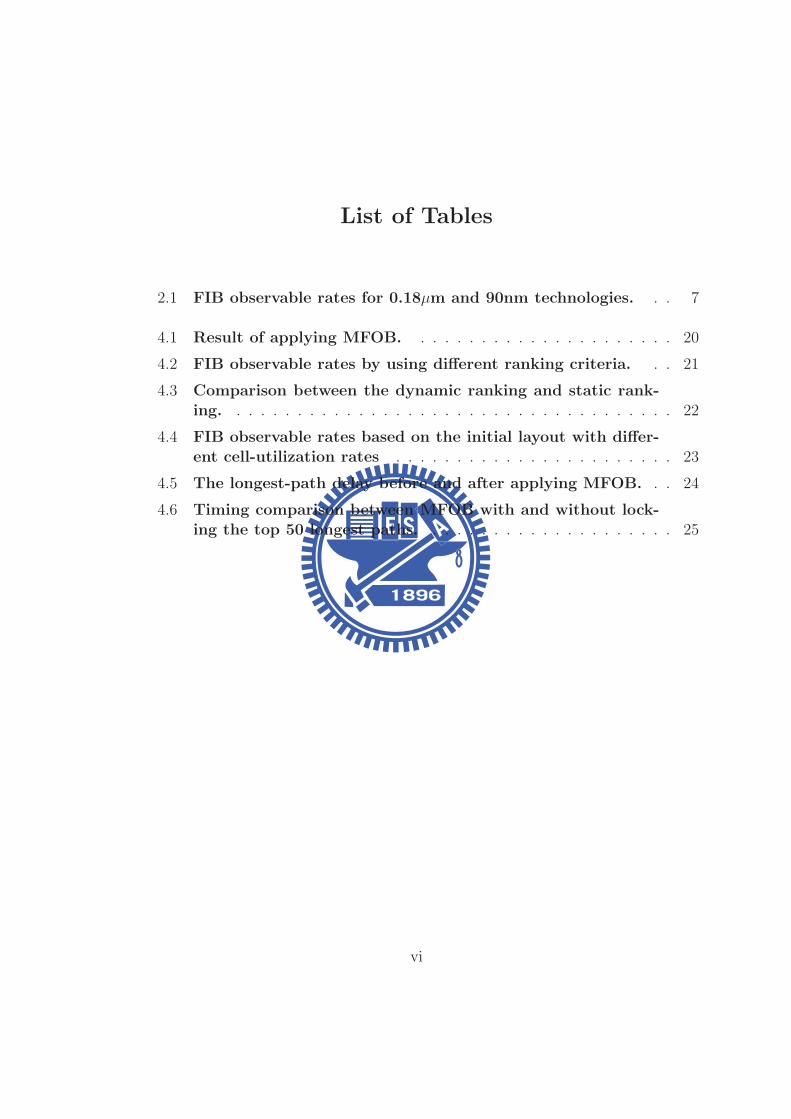
List of Tables
2.1 FIB observable rates for 0.18µm and 90nm technologies. . . 7
4.1 Result of applying MFOB. . . . . . . . . . . . . . . . . . . . . . 20
4.2 FIB observable rates by using different ranking criteria. . . 21
4.3 Comparison between the dynamic ranking and static rank-ing. . . . . . . . . . . . . . . . . . . . . . . . . . . . . . . . . . . . . 22
4.4 FIB observable rates based on the initial layout with differ-ent cell-utilization rates . . . . . . . . . . . . . . . . . . . . . . . 23
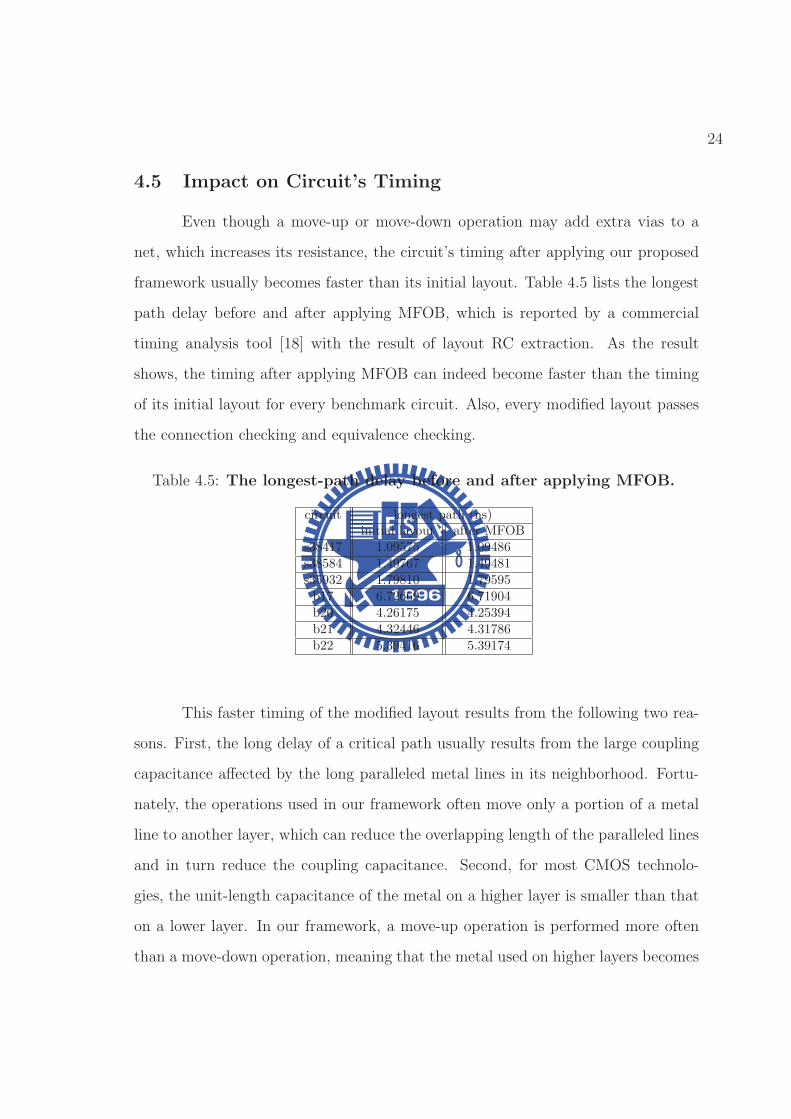
4.5 The longest-path delay before and after applying MFOB. . . 24
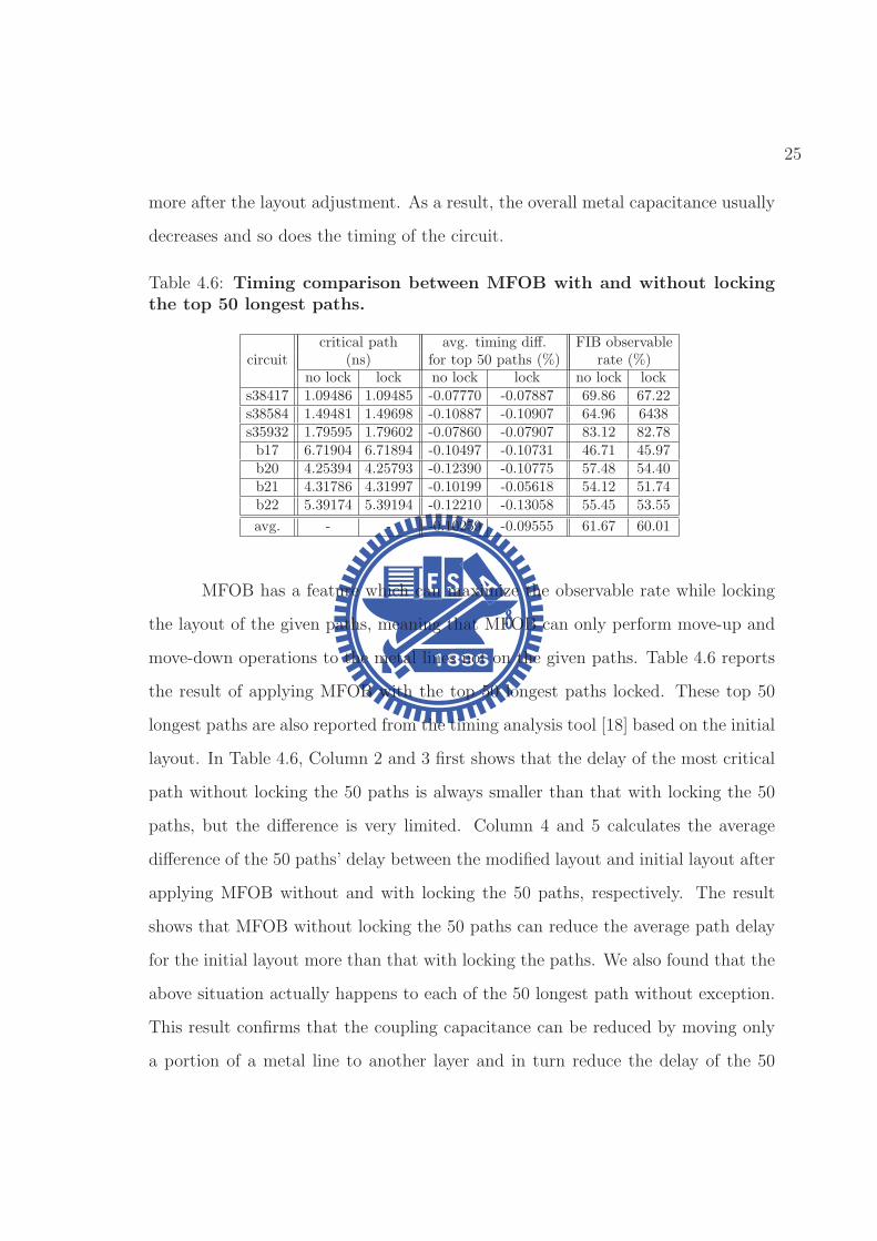
4.6 Timing comparison between MFOB with and without lock-ing the top 50 longest paths. . . . . . . . . . . . . . . . . . . . . 25
vi

List of Figures
2.1 An example of FIB probing using (a) FIB surface mill and(b) FIB deposition. . . . . . . . . . . . . . . . . . . . . . . . . . . 5
2.2 Illustration of a FIB hole. . . . . . . . . . . . . . . . . . . . . . . 6
2.3 Illustration of a net with metal lines locating in differentlayers. . . . . . . . . . . . . . . . . . . . . . . . . . . . . . . . . . . 7
3.1 Example of using a move-up operation. . . . . . . . . . . . . . 9
3.2 Example of using a move-down operation. . . . . . . . . . . . 10
3.3 Example of using both move-up and move-down operations. 11
3.4 The overall flow of the proposed framework. . . . . . . . . . . 12
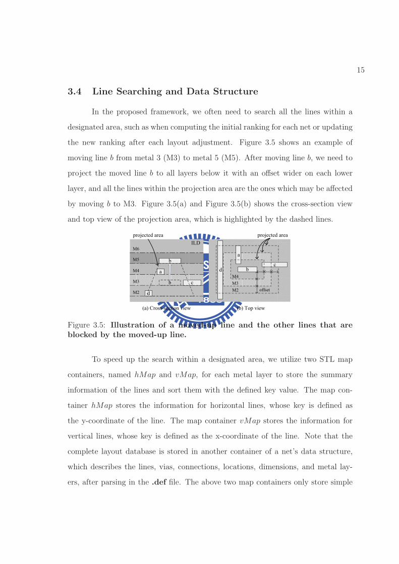
3.5 Illustration of a moved-up line and the other lines that areblocked by the moved-up line. . . . . . . . . . . . . . . . . . . . 15
3.6 Example of using hMap and vMap to store the location ofeach line. . . . . . . . . . . . . . . . . . . . . . . . . . . . . . . . . 16
3.7 Illustration of the procedure calculating the number of block-ing lines for each interval. . . . . . . . . . . . . . . . . . . . . . . 17
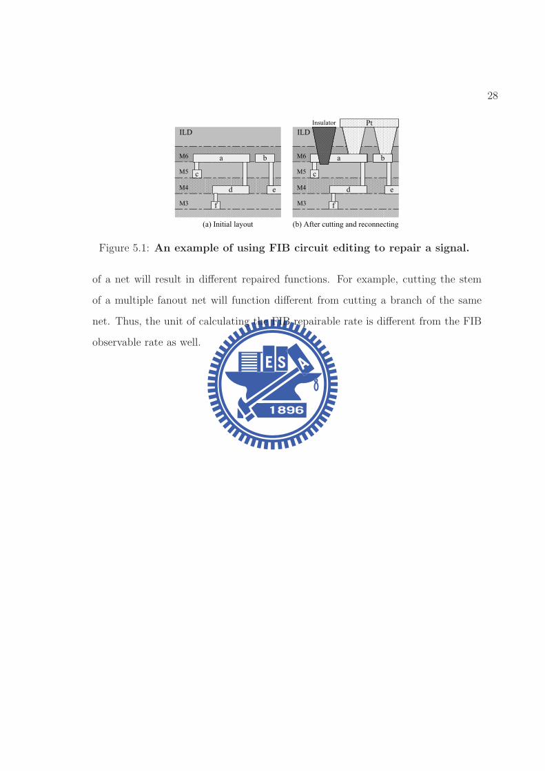
5.1 An example of using FIB circuit editing to repair a signal. . 28
vii

Chapter 1
Introduction
Due to the increasing complexity of modern designs and uncertainty of ad-
vanced process technologies, some design errors are difficult to detect by pure simu-
lation during the design phase and hence are more likely to escape from the current
design verification flow, which leads to a low first-silicon success rate for today’s
modern designs. As a result, post-silicon debug becomes a critical and necessary
step in the current design flow to identify the root causes of the escaped errors
based on the failed silicon chips and further fix them. Therefore, the effectiveness
and efficiency of the post-silicon debug will significantly affect the time and cost for
achieving the design closure [1][2].
Unlike pre-silicon debug where the value of internal signals can be obtained
easily through simulation, post-silicon debug has no direct access to the internal
signals of a failed chip and relies on specialized circuit features or physical probing
techniques to observe those internal signals. The specialized circuit features include
DFT (design for test) scan-based designs [3] and DFD (design for debug) trace-
buffer-based designs [1][4][5][6], which can dump the value of pre-selected flip-flops
or internal signals. However, those pre-selected signals may not be near the physical
fault locations and the provided visibility is only for a one-cycle snapshot or a limited
number of cycles. Therefore, physical probing techniques are still required to observe
the value of certain critical signals for post-silicon debug.
1
2
Physical probing techniques include electron beam (E-beam) probe [7], laser
voltage probe (LVP) [8], and focused ion beam (FIB) technique [9][10][11]. E-beam
probe can observe a signal on the top two metal layers through capacitive coupled
voltage contrast, and can further cooperate with FIB mill techniques to probe the
signal on the bottom metal layers from backside [12]. However, advanced process
technologies can easily contain more than 6 metal layers and hence the observable
signals through E-beam probe are limited. LVP is a backside probe technique and
measures a signal by transforming the amplitude of the reflected laser beam into a
voltage. The bandwidth of LVP is about 10 GHz and hence is especially suitable for
analyzing delay defect. However, for 65nm technologies, its transistor size is already
smaller than the resolution of LVP [13]. As a result, in order to use LVP in advance
technologies, additional type of cells need to be inserted into the circuit [13], or the
cells to be observed need to be replaced with larger cells [14], which results in extra
area overhead.
On the other hand, FIB technique utilizes ion beam to remove the covered
inter-layer dielectric (ILD) above the target signal and then deposit metal into the
hole to form a probe pad directly connecting the signal. This FIB probing requires
no area overhead to the design, is not only limited to the top metal layers, and is
relatively cost effective with shorter process time in current industry. In addition, the
FIB technique can also be used for circuit editing, such as cutting existing metal and
reconnecting it to a desired location (usually pre-placed spare cells). This circuit-
editing technique can quickly implement a simple circuit modification to repair the
failed chip without going through another tape-out and hence can significantly speed
up the whole silicon debug process.
When using FIB probing (or circuit editing), we need to make sure that the
metal of other signals above the observation location will not be touched or removed.
3
Otherwise, the probe pad may be connected to some unwanted signals or the original
circuit functionality may be changed. Unfortunately, while the technology node
continually scales, the resolution of FIB technologies does not scale accordingly. As
a result, for advance process technologies, the circuit layout becomes denser and
it is more difficult for FIB probing to pass through all the unwanted metals on
top of the observation location without modifying them, which significantly reduce
the percentage of signals that can be observed by FIB probing. [15] proposed an
automatic tool to efficiently identify the locations which can be used to perform the
desired FIB circuit editing. However, no current APR (automatic place and route)
tool can create a layout which is friendly for applying FIB probing or circuit editing,
if needed.
In this thesis, we propose a DFD framework name MFOB, which adjusts the
circuit layout to maximize the probability that a signal can be observed by FIB
probing. The layout adjustment is done through a few pre-defined actions, which
moves a small portion of the existing metal lines to different metal layers with new
vias, instead of performing a complete rerouting. Therefore, the proposed DFD
framework can be applied in conjunction with any APR tool and its impact on the
timing of critical paths is limited. Also, the proposed DFD framework can restrict
the layout adjustment on only the non-timing-critical paths if modifying certain
critical paths may violate their timing constraint. The experimental result based
on an 90nm technology has demonstrated that the proposed DFD framework can
effectively increase the number of signals being observable with FIB techniques while
the overall area and circuit performance remain the same. We further discuss the
necessary changes required in the framework when maximizing the number of the
signals being repairable with the FIB circuit editing in our future-work.
Chapter 2
Background of FIB
2.1 The mechanism of FIB
An FIB system operates in a similar manner as a scanning electron micro-
scope (SEM) or a transmission electron microscope (TEM) except that the FIB
system utilizes a focused beam of ions (gallium most of the time) instead of a beam
of electrons. When operating at a low beam current, a focused ion beam can be
used for imaging the sample surface with high resolution. When operating at a high
beam current, a focused ion beam can be used for milling the surface. Because the
ions are larger, heavier, slower, and positive compared to electrons, the ion beam
cannot easily penetrate within individual atoms of the sample and hence can more
easily break the chemical bonds of the substrate atoms, which makes FIB suitable
for surface milling [16].
Figure 2.1 illustrates an example of using FIB technique to observe a target
signal inside a chip. In Figure 2.1(a), the surface milling is performed by applying a
focused ion beam of Ga+ to hit the surface of inter-layer dielectric (ILD), break the
bonds of a certain amount of surface material, sputter out ions (mostly positive ions),
and gradually form a hole right above the target signal. Meanwhile, an electron beam
is applied to the surface to neutralize the sputtered positive ions, and sometimes
certain gas (such as XeF2) is also applied to assist the etching (mainly for preventing
the re-deposition of the sputtered surface material). Next, in Figure 2.1(b), FIB is
4
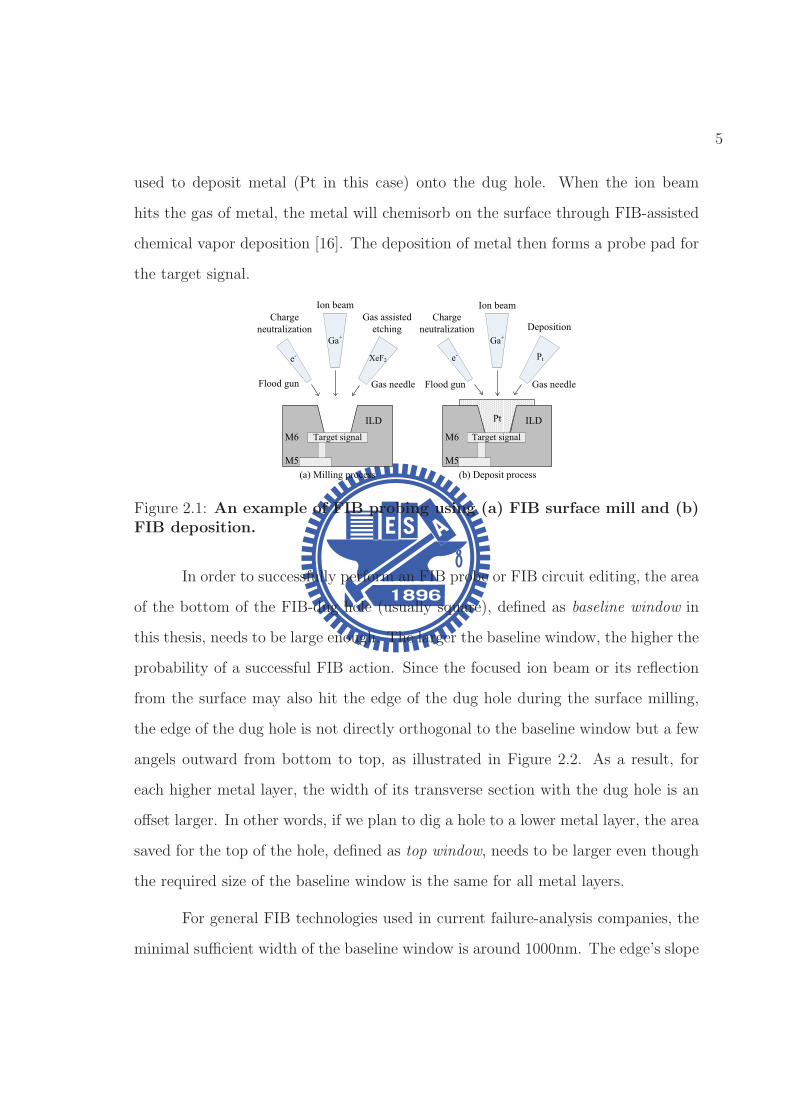
5
used to deposit metal (Pt in this case) onto the dug hole. When the ion beam
hits the gas of metal, the metal will chemisorb on the surface through FIB-assisted
chemical vapor deposition [16]. The deposition of metal then forms a probe pad for
the target signal.
���
�������� ������
���
������ ���� �������
��
����������� �������������
��
��
��
�������
�����������
������������
������
���������
�� !
��"
�������#
�������
�$
�������
����������� �� �����
���������
��
��"
�������#
�������
�$
Figure 2.1: An example of FIB probing using (a) FIB surface mill and (b)FIB deposition.
In order to successfully perform an FIB probe or FIB circuit editing, the area
of the bottom of the FIB-dug hole (usually square), defined as baseline window in
this thesis, needs to be large enough. The larger the baseline window, the higher the
probability of a successful FIB action. Since the focused ion beam or its reflection
from the surface may also hit the edge of the dug hole during the surface milling,
the edge of the dug hole is not directly orthogonal to the baseline window but a few
angels outward from bottom to top, as illustrated in Figure 2.2. As a result, for
each higher metal layer, the width of its transverse section with the dug hole is an
offset larger. In other words, if we plan to dig a hole to a lower metal layer, the area
saved for the top of the hole, defined as top window, needs to be larger even though
the required size of the baseline window is the same for all metal layers.
For general FIB technologies used in current failure-analysis companies, the
minimal sufficient width of the baseline window is around 1000nm. The edge’s slope
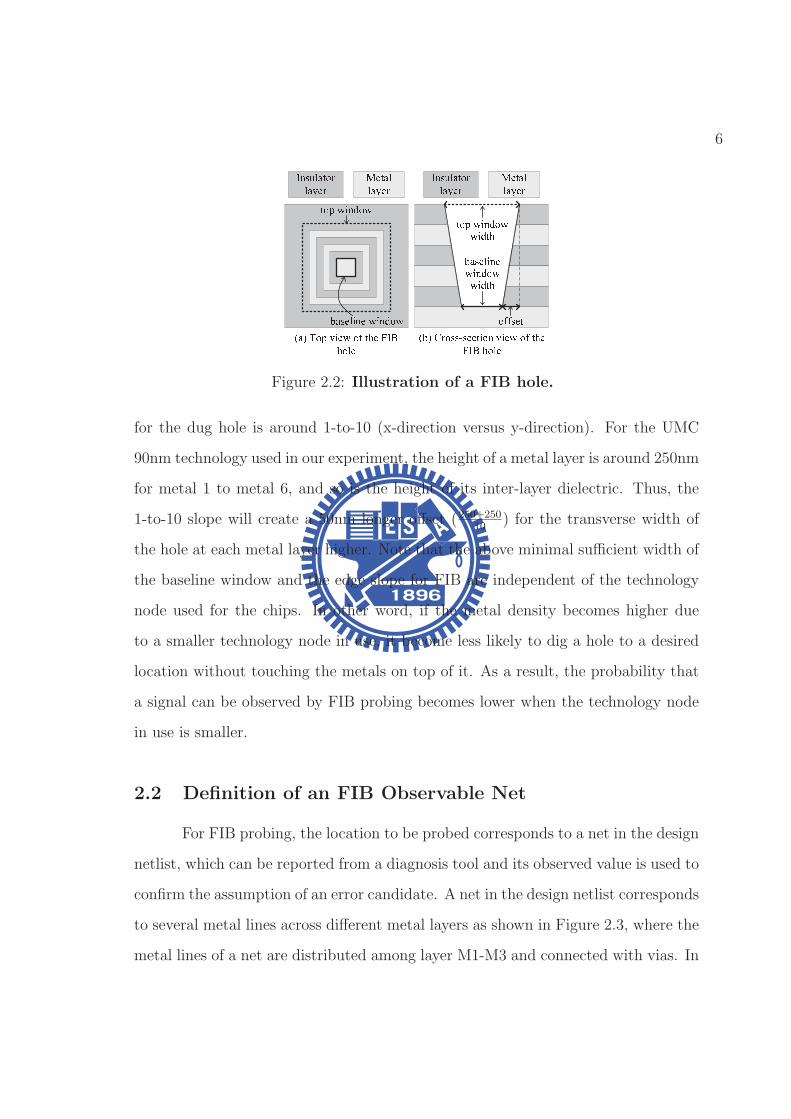
6
Figure 2.2: Illustration of a FIB hole.
for the dug hole is around 1-to-10 (x-direction versus y-direction). For the UMC
90nm technology used in our experiment, the height of a metal layer is around 250nm
for metal 1 to metal 6, and so is the height of its inter-layer dielectric. Thus, the
1-to-10 slope will create a 50nm longer offset (250+250
10) for the transverse width of
the hole at each metal layer higher. Note that the above minimal sufficient width of
the baseline window and the edge slope for FIB are independent of the technology
node used for the chips. In other word, if the metal density becomes higher due
to a smaller technology node in use, it become less likely to dig a hole to a desired
location without touching the metals on top of it. As a result, the probability that
a signal can be observed by FIB probing becomes lower when the technology node
in use is smaller.
2.2 Definition of an FIB Observable Net
For FIB probing, the location to be probed corresponds to a net in the design
netlist, which can be reported from a diagnosis tool and its observed value is used to
confirm the assumption of an error candidate. A net in the design netlist corresponds
to several metal lines across different metal layers as shown in Figure 2.3, where the
metal lines of a net are distributed among layer M1-M3 and connected with vias. In
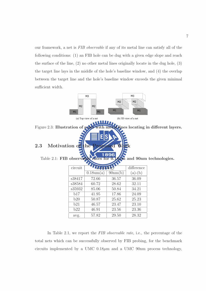
7
our framework, a net is FIB observable if any of its metal line can satisfy all of the
following conditions: (1) an FIB hole can be dug with a given edge slope and reach
the surface of the line, (2) no other metal lines originally locate in the dug hole, (3)
the target line lays in the middle of the hole’s baseline window, and (4) the overlap
between the target line and the hole’s baseline window exceeds the given minimal
sufficient width.
��
��
��
��
���������������� � ��������������� �
����
�� ��
�� ��
Figure 2.3: Illustration of a net with metal lines locating in different layers.
2.3 Motivation of the Proposed Work
Table 2.1: FIB observable rates for 0.18µm and 90nm technologies.
circuit technology difference0.18um(a) 90nm(b) (a)-(b)
s38417 72.66 36.57 36.09s38584 60.72 28.62 32.11s35932 85.06 50.84 34.21b17 41.95 17.86 24.09b20 50.87 25.62 25.23b21 46.57 23.47 23.10b22 46.91 23.56 23.36
avg. 57.82 29.50 28.32
In Table 2.1, we report the FIB observable rate, i.e., the percentage of the
total nets which can be successfully observed by FIB probing, for the benchmark
circuits implemented by a UMC 0.18µm and a UMC 90nm process technology,
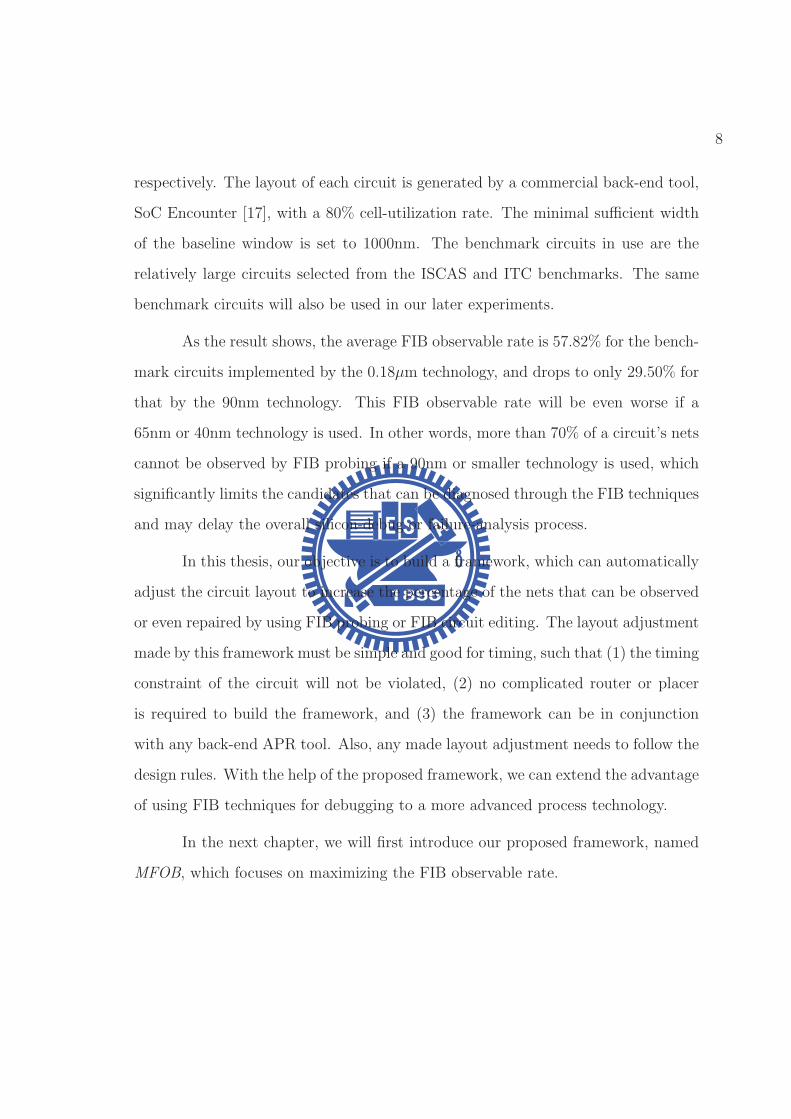
8
respectively. The layout of each circuit is generated by a commercial back-end tool,
SoC Encounter [17], with a 80% cell-utilization rate. The minimal sufficient width
of the baseline window is set to 1000nm. The benchmark circuits in use are the
relatively large circuits selected from the ISCAS and ITC benchmarks. The same
benchmark circuits will also be used in our later experiments.
As the result shows, the average FIB observable rate is 57.82% for the bench-
mark circuits implemented by the 0.18µm technology, and drops to only 29.50% for
that by the 90nm technology. This FIB observable rate will be even worse if a
65nm or 40nm technology is used. In other words, more than 70% of a circuit’s nets
cannot be observed by FIB probing if a 90nm or smaller technology is used, which
significantly limits the candidates that can be diagnosed through the FIB techniques
and may delay the overall silicon-debug or failure-analysis process.
In this thesis, our objective is to build a framework, which can automatically
adjust the circuit layout to increase the percentage of the nets that can be observed
or even repaired by using FIB probing or FIB circuit editing. The layout adjustment
made by this framework must be simple and good for timing, such that (1) the timing
constraint of the circuit will not be violated, (2) no complicated router or placer
is required to build the framework, and (3) the framework can be in conjunction
with any back-end APR tool. Also, any made layout adjustment needs to follow the
design rules. With the help of the proposed framework, we can extend the advantage
of using FIB techniques for debugging to a more advanced process technology.
In the next chapter, we will first introduce our proposed framework, named
MFOB, which focuses on maximizing the FIB observable rate.
Chapter 3
MFOB: Framework for Maximizing FIB
Observable Rate
3.1 Basic Operations for Adjusting Layout
���������������� ����������
��
��
��
���
��������������� ����������
��
��
��
��
�
��
��
���
�
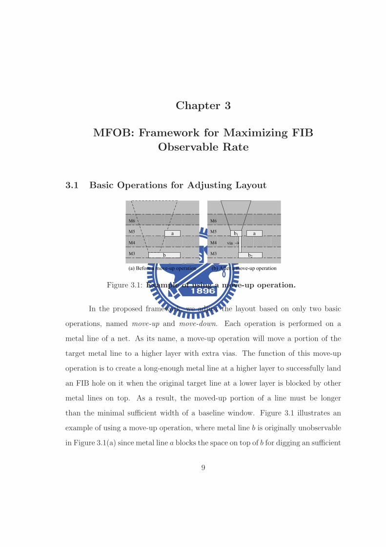
Figure 3.1: Example of using a move-up operation.
In the proposed framework, we adjust the layout based on only two basic
operations, named move-up and move-down. Each operation is performed on a
metal line of a net. As its name, a move-up operation will move a portion of the
target metal line to a higher layer with extra vias. The function of this move-up
operation is to create a long-enough metal line at a higher layer to successfully land
an FIB hole on it when the original target line at a lower layer is blocked by other
metal lines on top. As a result, the moved-up portion of a line must be longer
than the minimal sufficient width of a baseline window. Figure 3.1 illustrates an
example of using a move-up operation, where metal line b is originally unobservable
in Figure 3.1(a) since metal line a blocks the space on top of b for digging an sufficient
9
10
FIB hole (as shown by the dashed shape). After applying a move-up operation to b
in Figure 3.1(b), the moved-up portion of b can successfully land an sufficient FIB
hole and hence b becomes observable.
On the other hand, a move-down operation will move the target metal line
to the empty space on a lower layer with vias. The function of this move-down
operation is to remove the target line which originally blocks the observation of
other lines below it, such that certain lines below it may become observable after
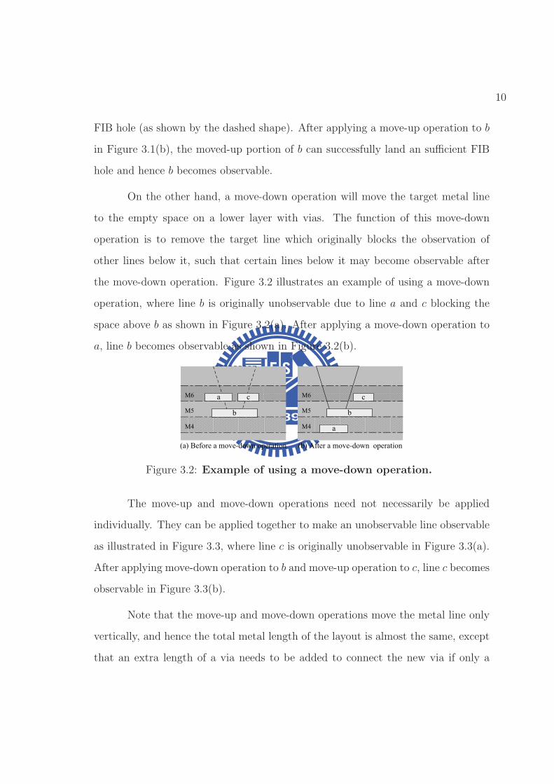
the move-down operation. Figure 3.2 illustrates an example of using a move-down
operation, where line b is originally unobservable due to line a and c blocking the
space above b as shown in Figure 3.2(a). After applying a move-down operation to
a, line b becomes observable as shown in Figure 3.2(b).
���������������� ������������
��
��
��
��������������� �������������
��
��
��
�
� �
�
� �
Figure 3.2: Example of using a move-down operation.
The move-up and move-down operations need not necessarily be applied
individually. They can be applied together to make an unobservable line observable
as illustrated in Figure 3.3, where line c is originally unobservable in Figure 3.3(a).
After applying move-down operation to b and move-up operation to c, line c becomes
observable in Figure 3.3(b).
Note that the move-up and move-down operations move the metal line only
vertically, and hence the total metal length of the layout is almost the same, except
that an extra length of a via needs to be added to connect the new via if only a
11
�������������� �������� ��
��
��
��
��
������������� ��������� ��
��
��
��
���
�
� �
�
��
��
� ��
�
Figure 3.3: Example of using both move-up and move-down operations.
portion of the line is moved. Also, all made move-up or move-down operations must
be feasible, i.e., following the design rules, such as the spacing between the moved
metal line and its new neighbors. In addition, some process technologies do not
allow stacked vias, meaning that a via can pass through only a certain number of
metal layers (3 in the UMC 90nm technology used in our experiments), which is
another constraint of using a move-up or move-down operation.
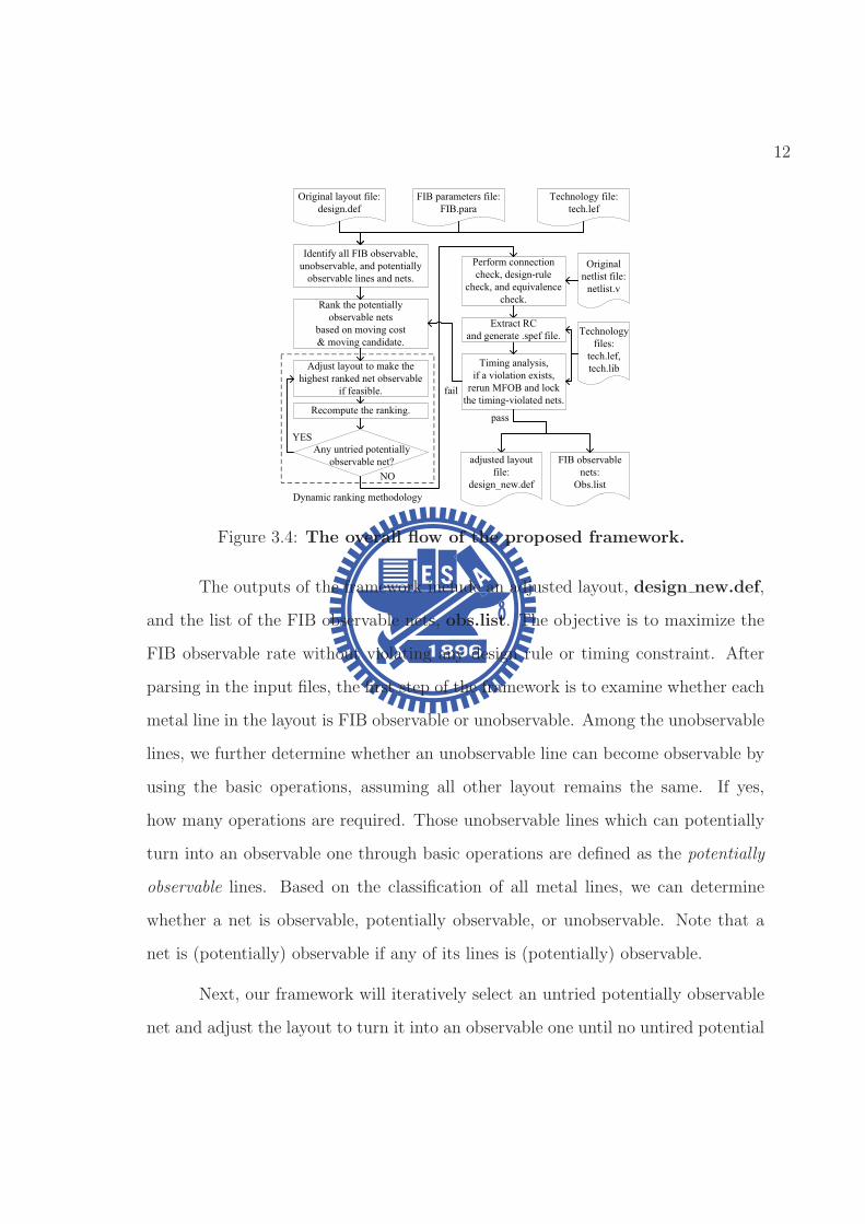
3.2 Overall Flow of MFOB
Figure 3.4 shows the overall flow of the proposed framework MFOB, which
requires the following input files.
• design.def: the file describing the layout of the design.
• FIB.para: the file describing the parameter for FIB, such as the minimal
sufficient width of a baseline window and the edge slope of a dug FIB hole.
• tech.lef: the file describing the physical-design information for the cell library,
such as pin location, layer, and via.
• netlist.v: the file describing gate-level netlist of the design.
• tech.lib: the file describing the timing information for the cell library.
12
�������������� ����
���������
��������������� ����
��������
������ ��������������������
���������������������������
�������������������������
�������������������
���������������
������������������
������������������
!"
#�$��������������������
�����������������������������
� � ��������
���������������������
%���������������������
&�
'������� ����
�������
(�� ������������
�������������)�����
������������*����������
������
!+�������,�
����������������� � ����
��$�����������
����
������-��.���
��������������
�����
��������
���������
�������� ����
���������
#��������������������
�������������/
���
����
'�������
�����
������� ��
��������'��������������
� ������������+������
������0������������
����������)�������������
Figure 3.4: The overall flow of the proposed framework.
The outputs of the framework include an adjusted layout, design new.def,
and the list of the FIB observable nets, obs.list. The objective is to maximize the
FIB observable rate without violating any design rule or timing constraint. After
parsing in the input files, the first step of the framework is to examine whether each
metal line in the layout is FIB observable or unobservable. Among the unobservable
lines, we further determine whether an unobservable line can become observable by
using the basic operations, assuming all other layout remains the same. If yes,
how many operations are required. Those unobservable lines which can potentially
turn into an observable one through basic operations are defined as the potentially
observable lines. Based on the classification of all metal lines, we can determine
whether a net is observable, potentially observable, or unobservable. Note that a
net is (potentially) observable if any of its lines is (potentially) observable.
Next, our framework will iteratively select an untried potentially observable
net and adjust the layout to turn it into an observable one until no untired potential
13
exists. In fact, adjusting the layout for a potentially observable net may eliminate the
chance of other potentially observable nets becoming an observable one. Therefore,
in order to maximize the FIB observable rate, we need to find a proper order for the
potentially observable nets being processed. In our framework, this process order of
the potentially observable nets is determined by a proposed ranking method, which
will be introduced in detail in Chapter 3.3. Note that the layout adjustment here is
performed based on a greedy-based principle. In other words, if an adjustment for a
potentially observable net may turn an originally observable net into an unobservable
or potentially observable one, the adjustment will not be performed. Any made
layout adjustment must increase the overall FIB observable rate.
After the layout adjustment stops, we will perform connection check, design-
rule check, and equivalence check to guarantee the correctness of the adjusted layout.
Then we perform the RC extraction for the layout and store the RC information
in the .spef file. Last, a timing analysis is applied based on the RC information,
design netlist, and technology files. If any timing violation occurs, we will rerun the
whole framework without adjusting the timing-violated nets and the critical paths
(if setup-time violated). In practice, timing violations rarely occur after our layout
adjustment. Its reasons will be discussed in Chapter 4.5.
3.3 Ranking Method
We rank the potentially observable nets based on two criteria, the number
of moving candidates of a net as the primary criterion and the moving cost of a
net as the secondary one. First, the number of moving candidates of a net is the
number of potentially observable lines contained by the net. If a net has only one
moving candidate, then we should better adjust the layout to save this net as early
as possible before its only left candidate become unobservable due to the layout

14
adjustment for the other nets. Thus, a net with less moving candidate will be
selected earlier by our ranking method.
Secondly, the moving cost of a line is the number of basic operations required
to turn the line into an observable one. The moving cost of a net is the smallest
moving cost among all its composed lines. In our ranking method, we prefer to first
select the net with the smallest moving cost, i.e., the easiest net to become observ-
able. This is because our objective is to maximize the total number of observable
nets with the limited routing resource. The less routing resource is spent for one net,
the more routing resource can be left for the other nets. In summary, our ranking
method will first select the net with the least moving candidates. If multiple nets
have the same moving candidates, the ranking method will select the net with the
smallest moving cost.
Once the layout adjustment is made for a net, the number of moving candi-
dates and the moving cost for the other nets may also change accordingly, meaning
that the ranking of nets changes as well. One way to handle this dynamic change is
to recompute the moving candidates and moving cost for the affected nets immedi-
ately after each layout adjustment, which is called the dynamic ranking. However,
this dynamic ranking method requires extra runtime to iteratively search the nets
affected by the layout adjustment and recompute their ranking. A more efficient
way is to rank the nets based on initial layout and use this initial ranking through-
out the entire layout-adjustment process, which is called the static ranking. We will
compare the effectiveness and efficiency between the dynamic ranking and static
ranking in Chapter 4.3.
15
3.4 Line Searching and Data Structure
In the proposed framework, we often need to search all the lines within a
designated area, such as when computing the initial ranking for each net or updating
the new ranking after each layout adjustment. Figure 3.5 shows an example of
moving line b from metal 3 (M3) to metal 5 (M5). After moving line b, we need to
project the moved line b to all layers below it with an offset wider on each lower
layer, and all the lines within the projection area are the ones which may be affected
by moving b to M3. Figure 3.5(a) and Figure 3.5(b) shows the cross-section view
and top view of the projection area, which is highlighted by the dashed lines.
�
��������� ��������
�����
��
�� �
�
�
���
�� �
������������
����
��
��
��
��
�
������ ������������� �������
Figure 3.5: Illustration of a moved-up line and the other lines that areblocked by the moved-up line.
To speed up the search within a designated area, we utilize two STL map
containers, named hMap and vMap, for each metal layer to store the summary
information of the lines and sort them with the defined key value. The map con-
tainer hMap stores the information for horizontal lines, whose key is defined as
the y-coordinate of the line. The map container vMap stores the information for
vertical lines, whose key is defined as the x-coordinate of the line. Note that the
complete layout database is stored in another container of a net’s data structure,
which describes the lines, vias, connections, locations, dimensions, and metal lay-
ers, after parsing in the .def file. The above two map containers only store simple
16
summary information of a line, such as the location of its end points, the line id,
its metal layer, and net id, to assist the search and the link to the complete layout
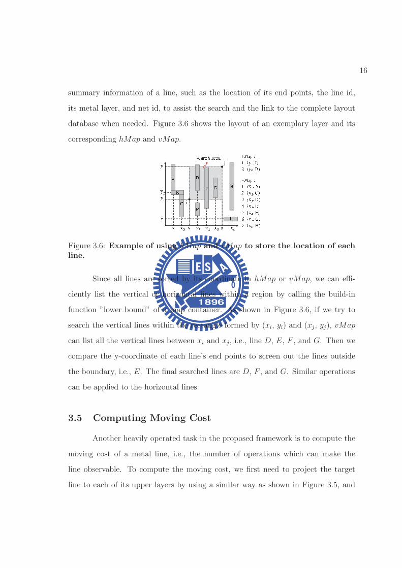
database when needed. Figure 3.6 shows the layout of an exemplary layer and its
corresponding hMap and vMap.
Figure 3.6: Example of using hMap and vMap to store the location of eachline.
Since all lines are sorted by its coordinate in hMap or vMap, we can effi-
ciently list the vertical or horizontal lines within a region by calling the build-in
function ”lower bound” of a map container. As shown in Figure 3.6, if we try to
search the vertical lines within the rectangle formed by (xi, yi) and (xj, yj), vMap
can list all the vertical lines between xi and xj , i.e., line D, E, F , and G. Then we
compare the y-coordinate of each line’s end points to screen out the lines outside
the boundary, i.e., E. The final searched lines are D, F , and G. Similar operations
can be applied to the horizontal lines.
3.5 Computing Moving Cost
Another heavily operated task in the proposed framework is to compute the
moving cost of a metal line, i.e., the number of operations which can make the
line observable. To compute the moving cost, we first need to project the target
line to each of its upper layers by using a similar way as shown in Figure 3.5, and
17
then search the lines within the projected area on each layer. Those searched lines
are the ones which may block the observation of the target line. Next, for each
searched blocking line, we project it back to the target line and mark the ends of
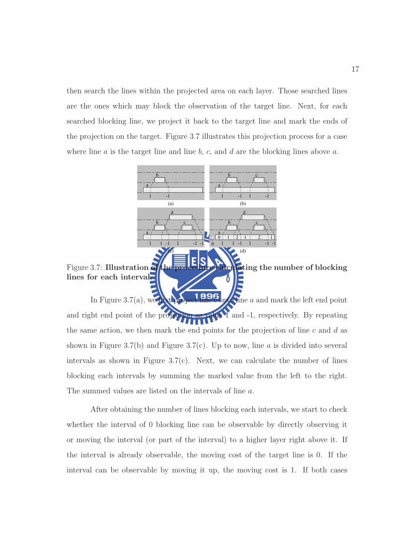
the projection on the target. Figure 3.7 illustrates this projection process for a case
where line a is the target line and line b, c, and d are the blocking lines above a.
���
� � ��� �� ��
���
� � ��� �� ���
� � � � � �
��
� ��
��
� ��� ��
� �
�
� �
Figure 3.7: Illustration of the procedure calculating the number of blockinglines for each interval.
In Figure 3.7(a), we first project line b onto line a and mark the left end point
and right end point of the projection as value 1 and -1, respectively. By repeating
the same action, we then mark the end points for the projection of line c and d as
shown in Figure 3.7(b) and Figure 3.7(c). Up to now, line a is divided into several
intervals as shown in Figure 3.7(c). Next, we can calculate the number of lines
blocking each intervals by summing the marked value from the left to the right.
The summed values are listed on the intervals of line a.
After obtaining the number of lines blocking each intervals, we start to check
whether the interval of 0 blocking line can be observable by directly observing it
or moving the interval (or part of the interval) to a higher layer right above it. If
the interval is already observable, the moving cost of the target line is 0. If the
interval can be observable by moving it up, the moving cost is 1. If both cases

18
fail, we need to merge the interval of 0 blocking line with the interval of 1 blocking
line, and then check whether the merged interval can be observable by moving all
the blocking lines down or plus moving the interval up. If the merged interval can
be observable by moving all the blocking lines down and those blocking lines can
indeed be feasibly moved down, the moving cost is equal to the number of blocking
lines in the merged interval. If the merged interval can be observable by moving
all the blocking lines down plus moving itself up, the moving cost is equal to the
number of blocking lines plus 1. If both cases fail, we need to merging the interval
into the interval with one more blocking line. We repeat the above process until the
interval with the most blocking lines is tried. If all above actions fail, the target line
is defined as unobservable.
With the help of obtaining the number of blocking lines for each interval, we
can systematically find a minimal number of move-up and/or move-down operations
to make a target line observable. Such a moving-cost computation avoids the enu-
meration and examination of all possible operation combinations, which significantly
improves the efficiency of the proposed framework.
Chapter 4
Experimental Results for Maximizing FIB
Observable Rate
The experiments in this chapter are conducted based on the same UMC 90nm
9-metal process technology and the same benchmark circuits as used in Table 2.1.
The initial layout of each circuit is generated by a commercial APR tool, SoC
Encounter [17]. Also, we ignore the observation for clock, reset, or scan enable
when applying the framework.
4.1 Before and After Applying MFOB
Table 4.1 reports the FIB observable rate based on a 1000nm minimum suf-
ficient width of the baseline window and a 1-to-10 edge slope of an FIB hole. The
cell-utilization rate is set to 80% to generate the initial layout with SoC Encounter.
Also, dynamic ranking is used in MFOB to determine the order of nets for layout
adjustment. In Table 4.1, Column 1 and 2 list the circuit name and its total number
of nets, respectively. Column 3 and 4 list the FIB observable rate before and after
applying our proposed framework MFOB, respectively. Their difference is listed on
Column 5. As the result shows, our proposed framework MFOB can successfully
increase the FIB observable rate from 29.50% to 61.67% in average by properly
adjusting the initial layout. The improvement in FIB observable rate ranges from
28.85% to 36.34% for different circuits. Note that this average 61.67% of the FIB
19
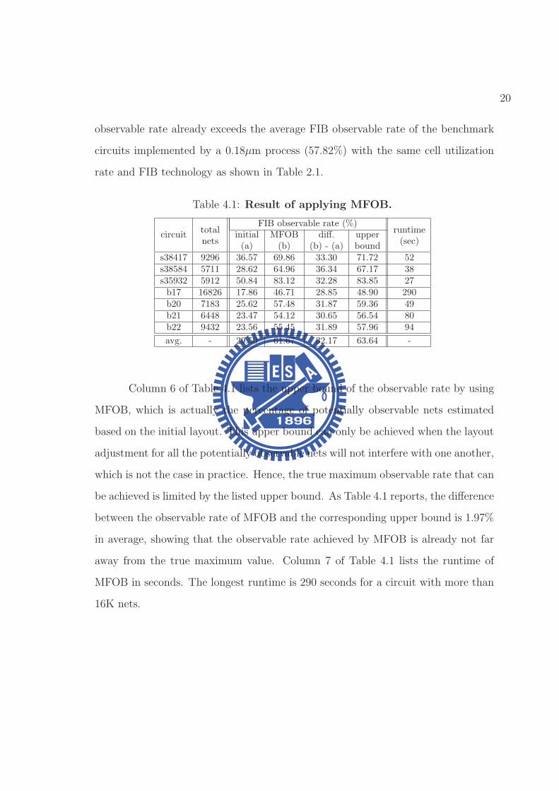
20
observable rate already exceeds the average FIB observable rate of the benchmark
circuits implemented by a 0.18µm process (57.82%) with the same cell utilization
rate and FIB technology as shown in Table 2.1.
Table 4.1: Result of applying MFOB.
FIB observable rate (%)circuit
totalinitial MFOB diff. upper
runtimenets
(a) (b) (b) - (a) bound(sec)
s38417 9296 36.57 69.86 33.30 71.72 52s38584 5711 28.62 64.96 36.34 67.17 38s35932 5912 50.84 83.12 32.28 83.85 27b17 16826 17.86 46.71 28.85 48.90 290b20 7183 25.62 57.48 31.87 59.36 49b21 6448 23.47 54.12 30.65 56.54 80b22 9432 23.56 55.45 31.89 57.96 94
avg. - 29.50 61.67 32.17 63.64 -
Column 6 of Table 4.1 lists the upper bound of the observable rate by using
MFOB, which is actually the percentage of potentially observable nets estimated
based on the initial layout. This upper bound can only be achieved when the layout
adjustment for all the potentially observable nets will not interfere with one another,
which is not the case in practice. Hence, the true maximum observable rate that can
be achieved is limited by the listed upper bound. As Table 4.1 reports, the difference
between the observable rate of MFOB and the corresponding upper bound is 1.97%
in average, showing that the observable rate achieved by MFOB is already not far
away from the true maximum value. Column 7 of Table 4.1 lists the runtime of
MFOB in seconds. The longest runtime is 290 seconds for a circuit with more than
16K nets.

21
4.2 Different Ranking Criteria
In the proposed ranking method for determining the order of nets to be
processed, we use the less moving candidates first as the primary criterion and the
lower moving cost first as the secondary criterion. Table 4.2 compares the proposed
ranking scheme with three different ranking scheme, named as R1, R2, and R3.
R1 uses the more moving candidates first as the primary criterion and the lower
moving cost first as the secondary one. R2 uses the less moving candidates first
as the primary criterion and the higher moving cost first as the second. R3 uses
the more moving candidates first as the primary criterion and the higher moving
cost first as the second one, which is completely opposite to the proposed ranking
scheme. The FIB observable rates achieved by using the proposed ranking scheme,
R1, R2, and R3 are reported on Column 2, 3, 4, and 5 of Table 4.2, respectively.
The other experiment settings are the same as Table 4.1.
Table 4.2: FIB observable rates by using different ranking criteria.
FIB observable rate (%)circuit
proposed R1 R2 R3s38417 69.86 69.34 69.74 69.24s38584 64.96 64.48 64.96 64.48s35932 83.12 82.83 83.11 82.82b17 46.71 45.87 46.67 45.83b20 57.48 57.06 57.48 57.03b21 54.12 53.34 54.06 53.29b22 55.45 54.65 55.38 54.62
avg. 61.67 61.08 61.63 61.04
As the result shows, the proposed ranking scheme can achieve higher observ-
able rate than any of the other three ranking schemes for every benchmark circuit.
On the other hand, the ranking scheme completely opposite to our proposed one
(R3) achieves the lowest observable rate for every benchmark circuit as well. This
22
result demonstrates that the ranking criteria used in our proposed framework are
indeed critical and helpful for maximizing the observable rate.
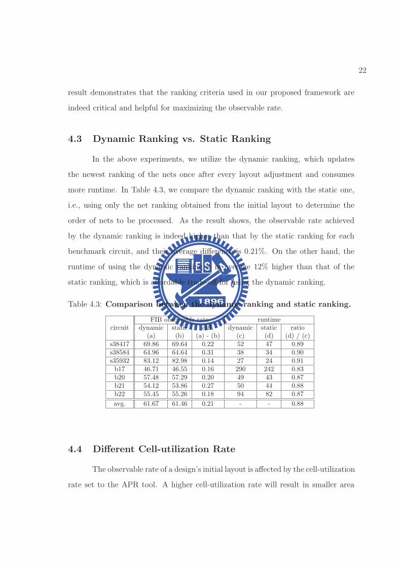
4.3 Dynamic Ranking vs. Static Ranking
In the above experiments, we utilize the dynamic ranking, which updates
the newest ranking of the nets once after every layout adjustment and consumes
more runtime. In Table 4.3, we compare the dynamic ranking with the static one,
i.e., using only the net ranking obtained from the initial layout to determine the
order of nets to be processed. As the result shows, the observable rate achieved
by the dynamic ranking is indeed higher than that by the static ranking for each
benchmark circuit, and their average difference is 0.21%. On the other hand, the
runtime of using the dynamic ranking is in average 12% higher than that of the
static ranking, which is affordable trade-off for using the dynamic ranking.
Table 4.3: Comparison between the dynamic ranking and static ranking.
FIB observable rate runtimecircuit dynamic static diff. dynamic static ratio
(a) (b) (a) - (b) (c) (d) (d) / (c)s38417 69.86 69.64 0.22 52 47 0.89s38584 64.96 64.64 0.31 38 34 0.90s35932 83.12 82.98 0.14 27 24 0.91b17 46.71 46.55 0.16 290 242 0.83b20 57.48 57.29 0.20 49 43 0.87b21 54.12 53.86 0.27 50 44 0.88b22 55.45 55.26 0.18 94 82 0.87
avg. 61.67 61.46 0.21 - - 0.88
4.4 Different Cell-utilization Rate
The observable rate of a design’s initial layout is affected by the cell-utilization
rate set to the APR tool. A higher cell-utilization rate will result in smaller area
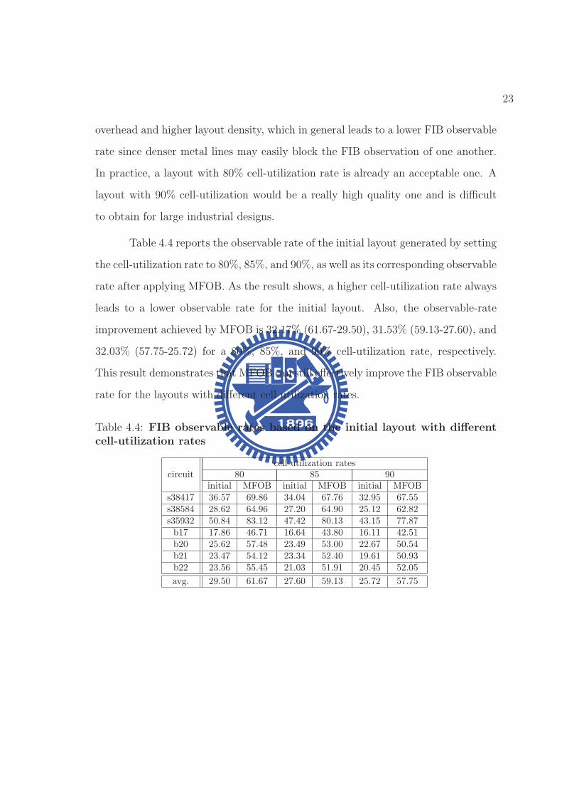
23
overhead and higher layout density, which in general leads to a lower FIB observable
rate since denser metal lines may easily block the FIB observation of one another.
In practice, a layout with 80% cell-utilization rate is already an acceptable one. A
layout with 90% cell-utilization would be a really high quality one and is difficult
to obtain for large industrial designs.
Table 4.4 reports the observable rate of the initial layout generated by setting
the cell-utilization rate to 80%, 85%, and 90%, as well as its corresponding observable
rate after applying MFOB. As the result shows, a higher cell-utilization rate always
leads to a lower observable rate for the initial layout. Also, the observable-rate
improvement achieved by MFOB is 32.17% (61.67-29.50), 31.53% (59.13-27.60), and
32.03% (57.75-25.72) for a 80%, 85%, and 90% cell-utilization rate, respectively.
This result demonstrates that MFOB can still effectively improve the FIB observable
rate for the layouts with different cell utilization rates.
Table 4.4: FIB observable rates based on the initial layout with differentcell-utilization rates
cell-utilization ratescircuit 80 85 90
initial MFOB initial MFOB initial MFOBs38417 36.57 69.86 34.04 67.76 32.95 67.55s38584 28.62 64.96 27.20 64.90 25.12 62.82s35932 50.84 83.12 47.42 80.13 43.15 77.87b17 17.86 46.71 16.64 43.80 16.11 42.51b20 25.62 57.48 23.49 53.00 22.67 50.54b21 23.47 54.12 23.34 52.40 19.61 50.93b22 23.56 55.45 21.03 51.91 20.45 52.05
avg. 29.50 61.67 27.60 59.13 25.72 57.75
24
4.5 Impact on Circuit’s Timing
Even though a move-up or move-down operation may add extra vias to a
net, which increases its resistance, the circuit’s timing after applying our proposed
framework usually becomes faster than its initial layout. Table 4.5 lists the longest
path delay before and after applying MFOB, which is reported by a commercial
timing analysis tool [18] with the result of layout RC extraction. As the result
shows, the timing after applying MFOB can indeed become faster than the timing
of its initial layout for every benchmark circuit. Also, every modified layout passes
the connection checking and equivalence checking.
Table 4.5: The longest-path delay before and after applying MFOB.
circuit longest path (ns)initial layout after MFOB
s38417 1.09575 1.09486s38584 1.49767 1.49481s35932 1.79810 1.79595b17 6.72669 6.71904b20 4.26175 4.25394b21 4.32446 4.31786b22 5.39416 5.39174
This faster timing of the modified layout results from the following two rea-
sons. First, the long delay of a critical path usually results from the large coupling
capacitance affected by the long paralleled metal lines in its neighborhood. Fortu-
nately, the operations used in our framework often move only a portion of a metal
line to another layer, which can reduce the overlapping length of the paralleled lines
and in turn reduce the coupling capacitance. Second, for most CMOS technolo-
gies, the unit-length capacitance of the metal on a higher layer is smaller than that
on a lower layer. In our framework, a move-up operation is performed more often
than a move-down operation, meaning that the metal used on higher layers becomes
25
more after the layout adjustment. As a result, the overall metal capacitance usually
decreases and so does the timing of the circuit.
Table 4.6: Timing comparison between MFOB with and without lockingthe top 50 longest paths.
critical path avg. timing diff. FIB observablecircuit (ns) for top 50 paths (%) rate (%)
no lock lock no lock lock no lock locks38417 1.09486 1.09485 -0.07770 -0.07887 69.86 67.22s38584 1.49481 1.49698 -0.10887 -0.10907 64.96 6438s35932 1.79595 1.79602 -0.07860 -0.07907 83.12 82.78b17 6.71904 6.71894 -0.10497 -0.10731 46.71 45.97b20 4.25394 4.25793 -0.12390 -0.10775 57.48 54.40b21 4.31786 4.31997 -0.10199 -0.05618 54.12 51.74b22 5.39174 5.39194 -0.12210 -0.13058 55.45 53.55
avg. - - -0.10259 -0.09555 61.67 60.01
MFOB has a feature which can maximize the observable rate while locking
the layout of the given paths, meaning that MFOB can only perform move-up and
move-down operations to the metal lines not on the given paths. Table 4.6 reports
the result of applying MFOB with the top 50 longest paths locked. These top 50
longest paths are also reported from the timing analysis tool [18] based on the initial
layout. In Table 4.6, Column 2 and 3 first shows that the delay of the most critical
path without locking the 50 paths is always smaller than that with locking the 50
paths, but the difference is very limited. Column 4 and 5 calculates the average
difference of the 50 paths’ delay between the modified layout and initial layout after
applying MFOB without and with locking the 50 paths, respectively. The result
shows that MFOB without locking the 50 paths can reduce the average path delay
for the initial layout more than that with locking the paths. We also found that the
above situation actually happens to each of the 50 longest path without exception.
This result confirms that the coupling capacitance can be reduced by moving only
a portion of a metal line to another layer and in turn reduce the delay of the 50

26
longest paths even though the layout of these 50 longest paths is not changed. In
addition, Column 6 and 7 show that the FIB observable achieved by not locking the
50 paths is in average 1.66% higher than that locking the 50 paths.
Chapter 5
Future Work: Maximizing FIB Repairable Rate
The above chapters, we have introduced how to maximize the number of nets
being observable by FIB probing for a given layout. In this chapter, we would like
to further discuss the differences that the proposed framework may need to make for
maximizing the number of nets being repairable by FIB circuit editing. To repair
a signal, two actions need to be performed. The first action is to reconnect the cut
signal to a new one, which is done by digging an FIB hole onto each of the target
line and the line connecting to, filling metal into the two holes, and connecting them
together. The second action is to cut the connection of the original signal source,
which is done by digging an FIB hole, breaking through the target metal line and
then filling the hole with insulator. Figure 5.1 illustrates an example of cutting the
signal a and reconnect it to a new signal b. Thus, in order to successfully apply the
FIB circuit editing to repair a signal, we need to dug two FIB holes to the metal lines
of the signal, one for cutting the original connection and the other for reconnecting.
Note that the cutting hole and the reconnecting hole can physically locate next to
each other without interfering.
As a result, when building the framework for maximizing the FIB repairable
rate, we need to check not only whether an FIB hole can successfully land onto a
metal line (as in MFOB) but also how many FIB holes can successfully land onto
the metal line. Also, when using the FIB circuit editing, cutting different locations
27
28
���������������
� �
��
��
��
����������������������������������
��
�
�
� �
��
��
��
�� �
����������
�
� �
� �
� �
��
��
� �
Figure 5.1: An example of using FIB circuit editing to repair a signal.
of a net will result in different repaired functions. For example, cutting the stem
of a multiple fanout net will function different from cutting a branch of the same
net. Thus, the unit of calculating the FIB repairable rate is different from the FIB
observable rate as well.
Chapter 6
Conclusions
In this thesis, we have proposed a DFD framework, named MFOB, which can
increase the FIB observable rate by using a greedy-based algorithm to iteratively
adjust the layout for a selected signal. An effective ranking scheme has also been
developed to generate a proper order of signals for layout adjustment and maximize
the resulting observable rate. A series of experiments have demonstrated that the
targeted observable rate of the initial layout can be significantly increased without
violating any design rule. Meanwhile, the adjusted layout can remain the same
size and its timing can even become slightly better. Its runtime is also within
a reasonable range for a software dealing with the complete layout database. In
addition, the proposed frameworks can be easily integrated into the current design
flow and applied in conjunction with any commercial APR tool.
29
Bibliography
[1] M. Abramovici, P. Bradley, K. Dwarakanath, P. Levin, G. Memmi, and D. Miller,”A Reconfigurable Design-for-Debug Infrastructure for SoCs”, Design Automation
Conference, pp. 7-12, 2006.
[2] R. Goering, ”Post-Silicon Debugging Worth a Second Look”, EETimes, Feb. 05,2007.
[3] M. L. Bushnell and V. D. Agrawal, Essentials of Electronic Testing, Kluwer, Boston,2000.
[4] E. Anis and N. Nicolico, ”On Using Lossless Compression of Debug Data in Em-bedded Logic Analyis”, International Test Conference, pp. 1-10, 2007.
[5] E. Anis and N. Nicolico, ”Low Cost Debug Architecture using Lossy Compressionfor Silicon Debug”, Design Automation, and Test in Europe, pp. 1-6, 2007.
[6] J.-S. Yang and Nur A. Touba, ”Expanding Trace Buffer Observation Window forIn-System Silicon Debug through Selective Capture”, VLSI Tset Symposium, pp.345-351, 2008.
[7] C. Shawn, C. C. Tsao, and T. R. Lundquist, ”Measuring back-side voltage of anintegrated circuit”, U.S. Patent 6,872,581 B2, 2005.
[8] W.-M. Yee, M. Paniicia, T. Eiles, and V. Rao, ”Laser Voltage Probe (LVP): a NovelOptical Probing Technology for Flip-Chip Package Microprocessors”, InternationSymposium on the Physical and Failure Analysis of Integrated Circuits, pp. 15-20,1999.
[9] M. T. Abramo and L. L. Hahn, ”The Application of Advanced Techniques forComplex Focused-Ion-Beam Device Modification”, Microelectronics Reliability, Vol.36, Issues 11-12, pp. 1775-1778, 1996.
[10] C. G. Talbot, M. Park, N. Richardson, P. Alto, and D. Masnaghetti, ”IC Modifica-tion with Foucused Ion Beam System”, U.S. patent 5,140,164, 1992.
[11] D. C. Shaver and B. W. Ward, ”Integrated Circuit Diagnosis Using FoucusedIon Beams”, Journal of Vacuum Science & Technology B; Microelectronics and
Nanometer Structures, Vol. 4, Issuse 1, pp. 185-188, 1986.
30
31
[12] R. Schlangen, R. Leihkauf, U. Kerst, C. Boit, and B. Kruger, ”Functional IC Anal-ysis Through Chip Backside With Nano Scale Resolution - E-Beam Probing inFIB Trenches to STI Level”, International Symposium on the Physical and Failure
Analysis of Integrated Circuits, pp. 35-38, 2007.
[13] J. Nonaka, ”Design for Failure Analysis by using LVP Measurement Elements”,Semi Technology Symposium, pp45-48, 2003.
[14] J. Nonaka, T. Ishiyama, and K. Shigeta, ”Design for Failure Analysis insertingReplacement-type Observation Points for LVP”, International Testing Conference,pp. 1-10, 2009.
[15] Y.-R. Wu, S.-Y. Kao, and S.-A. Hwang, ”Minimizing ECO routing for FIB”, VLSIDesign Automation and Test, pp. 351-354, 2010.
[16] FEI Company, ”Focused Ion Beam Technology, Capabilites and Applications”,http://www.fei.com.
[17] Cadence, ”Encounder R©User Guide,” version 8.1.2, 2009.
[18] Synopsys, PrimeTime, version B-2008.12-SP3-2, 2009.