Embed Size (px)
Citation preview

TitlePlasma etching mechanisms in the fabrication ofhigh-aspect-ratio microstructures in stackedlayers of different materials
Author(s) 岩瀬, 拓
Citation
Issue Date
Text Version ETD
URL https://doi.org/10.18910/73566
DOI 10.18910/73566
rights
Note
Osaka University Knowledge Archive : OUKAOsaka University Knowledge Archive : OUKA
https://ir.library.osaka-u.ac.jp/repo/ouka/all/
Osaka University

-1-
Doctoral Dissertation
Plasma etching mechanisms
in the fabrication of high-aspect-ratio microstructures
in stacked layers of different materials
異種積層膜高アスペクト比微細構造
プラズマエッチング機構の解明
Taku Iwase
July 2019
Graduate School of Engineering,
Osaka University

-2-
Contents
1. INTRODUCTION .................................................................................................................. 4
1.1 BACKGROUND ........................................................................................................................ 4
1.2 REACTIVE ION ETCHING .......................................................................................................... 5
1.2.1 Selected breakthroughs in RIE development ............................................................. 6
1.2.2 Overview of semiconductor device technology nodes ............................................. 10
1.3 HIGH-ASPECT-RATIO ETCHING............................................................................................... 10
1.3.1 Aspect-ratio-dependent etching (ARDE) .................................................................. 12
1.3.2 Effects of IEDF/IADF on HAR etching ...................................................................... 13
1.3.3 Ion and neutral transport inside HAR holes ............................................................. 14
1.3.4 Charging and charge buildup ................................................................................... 16
1.3.5 Abnormal profiles (bowing, striation, distortion, twisting) ......................................... 18
1.4 STACKED MULTILAYER ETCHING ............................................................................................ 21
1.5 OBJECTIVES OF THIS STUDY.................................................................................................. 22
1.6 ORGANIZATION OF THIS DISSERTATION .................................................................................. 23
REFERENCES............................................................................................................................. 24
2. DEMONSTRATION OF HIGH-ASPECT-RATIO MULTILAYER ETCHING IN HBR/CH3F-
BASED GAS PLASMAS WITH N2 GAS ADDITION ................................................................ 32
2.1 INTRODUCTION ..................................................................................................................... 32
2.2 EXPERIMENTAL PROCEDURE ................................................................................................. 33
2.3 RESULTS AND DISCUSSION ................................................................................................... 35
2.3.1 Gas mixing for continuous etching process ............................................................. 35
2.3.2 Equilibrium simulation with additional gas ................................................................ 36
2.3.3 Surface composition dependence on-wafer temperature ........................................ 37
2.3.4 Etching profile evaluation ......................................................................................... 39
2.3.5 Modeling a surface reaction ..................................................................................... 40
2.4 CONCLUSION ....................................................................................................................... 41
REFERENCES............................................................................................................................. 42
3. EFFECT OF TEMPERATURE ON COMPOSITION OF DEPOSITION LAYER IN
HBR/N2/CH3F-BASED GAS PLASMAS .................................................................................. 44
3.1 INTRODUCTION ..................................................................................................................... 44
3.2 EXPERIMENTAL PROCEDURE ................................................................................................. 45
3.3 RESULTS AND DISCUSSION ................................................................................................... 46

-3-
3.3.1 Temperature dependence of etching rate ................................................................ 46
3.3.2 Surface composition analysis ................................................................................... 48
3.4 CONCLUSION ....................................................................................................................... 53
REFERENCES............................................................................................................................. 54
4. ELIMINATING DEPENDENCE OF HOLE DEPTH ON ASPECT RATIO BY FORMING
AMMONIUM BROMIDE IN HBR/CH3F-BASED GAS PLASMAS ............................................ 56
4.1 INTRODUCTION ..................................................................................................................... 56
4.2 EXPERIMENTAL PROCEDURE ................................................................................................. 57
4.3 RESULTS AND DISCUSSION ................................................................................................... 59
4.3.1 Temperature dependence of etching rate ................................................................ 59
4.3.2 Temperature dependence of etched-hole profile ..................................................... 61
4.3.3 Temperature dependence of surface composition inside holes ............................... 62
4.3.4 Formation process of ammonium bromide ............................................................... 64
4.3.5 Aspect-ratio-dependent etching ............................................................................... 65
4.4 CONCLUSION ....................................................................................................................... 67
REFERENCES............................................................................................................................. 69
5. DEPOSITION PROFILE OF AMMONIUM BROMIDE IN HBR/N2 GAS PLASMAS FOR
HIGH-ASPECT-RATIO STRUCTURE ..................................................................................... 71
5.1 INTRODUCTION ..................................................................................................................... 71
5.2 EXPERIMENTAL PROCEDURE ................................................................................................. 72
5.3 RESULTS AND DISCUSSION ................................................................................................... 74
5.3.1 Temperature dependence of ammonium bromide deposition ................................. 74
5.3.2 Deposition rate distribution in the macro cavity........................................................ 75
5.3.3 Formation model for ammonium bromide on solid surface ...................................... 76
5.3.4 Comparing NH4Br formation model with experimental result ................................... 78
5.4 CONCLUSION ....................................................................................................................... 80
APPENDIX .................................................................................................................................. 81
REFERENCES............................................................................................................................. 83
6. CONCLUSION .................................................................................................................... 85
LIST OF PUBLICATIONS ....................................................................................................... 87
ACKNOWLEDGMENTS ......................................................................................................... 89

-4-
1. Introduction
1.1 Background
The semiconductor device industry is a fast-growing fundamental industry; its
market size in 2017 totaled approximately $420 billion [1]. At present, dry processing
technologies are indispensable for its development. In fact, most steps in device
fabrication use dry processing technologies based on plasma-enhanced or -assisted
physicochemical reactions. This means that further research on plasma technologies is a
driving force for further advancement and innovation [2].
Ten years ago, Abe et al. reviewed the development of plasma etching
technologies for fabricating semiconductor devices [3]. Since then, much progress has
been made in this research field. This review covers plasma etching technologies for
conventional semiconductor fabrication involving high-aspect-ratio (HAR) contacts and
reliable Cu/low-dielectric constant dielectrics (Cu/low-k) interconnects. It points out the
demand for reduced plasma-induced damage and for more precise control of the critical
dimensions (CDs) and etching feature profiles. The concerns about damage [4] and CD
control [5,6] were recently extensively reviewed. To consider the wider capabilities of
plasma processes, the historical background of dry processing is reviewed again here.
In particular, the period during which semiconductor manufacturing introduced
plasma technology, including non-thermal processes such as reactive ion etching (RIE)
and plasma-enhanced thin film deposition, witnessed epoch-making inventions and
discoveries, equivalent to those that ushered in the nanotechnology era. Plasma-enhanced
or -assisted physicochemical reactions are characterized by a lack of directional
thermodynamic minima to reach the state of thermal equilibrium. Energetic particles,
such as electrons, ions, radicals, neutrals, and photons, which are generated in the plasma
state of precursor gases, assist the reactions independently of thermodynamic minima and
thermal equilibrium states. Thus, one can call this “nonequilibrium dynamics.” The time
evolution of the reaction behavior is nonlinear dynamics. The topics of ion-induced
reactions and photochemistry are discussed in multidisciplinary scientific areas, requiring
that in situ reactions be monitored and analyzed in real time using emerging analytical
techniques.
-5-
1.2 Reactive ion etching
Dry etching evolved into an indispensable technique in semiconductor
manufacturing for miniaturization, and the maturation of fast anisotropic dry etching
techniques spawned the next wave of system miniaturization in a variety of commercial
products [7]. At the dawn of the dry process age, many new technologies emerged in
multidisciplinary approaches. Most importantly, plasma science and technology
significantly contributed to the indispensable development of high-volume dry processing.
In the 1960s, the semiconductor industry emerged from the era of wet processing
at minimum gate lengths of approximately 10 μm [8]. In the late 1960s, dry etching using
photoresist strippers, i.e., “plasma ashing,” began to appear in wafer fabrication lines [9].
In the mid 1970s, the industry moved to the large-scale integrated circuit (LSI) era. RIE
techniques using directed ion beams of reactive plasmas with high-resolution and
anisotropy emerged in processing [9]. In the early 1980s, advances in manufacturing
technology dramatically increased manufacturing yield and factory efficiency, and
thereafter quality became a major concern [8].
Advances in RIE emerged from using a combination of a chemical reaction and
a physical action. Sputtering processing (and ion milling) began using a plasma of inert
gases. Directed ions colliding more on the horizontal surface than on the sidewalls results
in anisotropic etching in which the etching rate is higher in the vertical direction. The
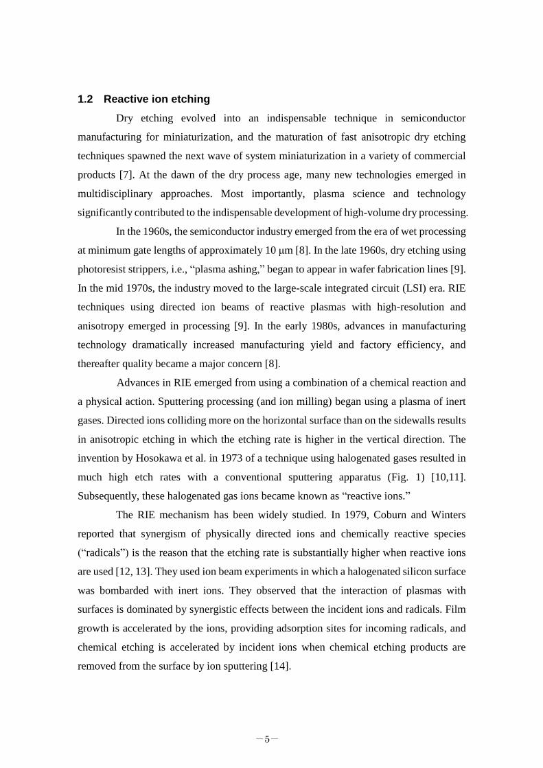
invention by Hosokawa et al. in 1973 of a technique using halogenated gases resulted in
much high etch rates with a conventional sputtering apparatus (Fig. 1) [10,11].
Subsequently, these halogenated gas ions became known as “reactive ions.”
The RIE mechanism has been widely studied. In 1979, Coburn and Winters
reported that synergism of physically directed ions and chemically reactive species
(“radicals”) is the reason that the etching rate is substantially higher when reactive ions
are used [12, 13]. They used ion beam experiments in which a halogenated silicon surface
was bombarded with inert ions. They observed that the interaction of plasmas with
surfaces is dominated by synergistic effects between the incident ions and radicals. Film
growth is accelerated by the ions, providing adsorption sites for incoming radicals, and
chemical etching is accelerated by incident ions when chemical etching products are
removed from the surface by ion sputtering [14].

-6-
In addition to ions, the physical actions in chemical reactions have been
considered. For instance, photolysis of organic molecules can be classified in terms of
physical action. In 1968, Kumagawa et al. reported epitaxial Si growth with light
irradiation from a mercury lamp [15]. They argued that precursors of SiCl4 can be
dissociated by ultraviolet light irradiation, reducing the activation energy for crystal
growth. The dissociation was initially monitored by using spectroscopic analysis, such as
infrared absorption [16]. Chemical reactions were assessed as thermal equilibrium
reactions; today, nonequilibrium reactions are attracting research attention. Not only light
but also electrons and ions had become the central focus of research on dry processing.
Whenever dry processing is conducted, the synergism of physical collisions and chemical
reactions must be kept in mind.
Ions can move with acceleration under electric fields. This property is useful for
two purposes: (i) acceleration of bombardment energy and (ii) transport of reactants
toward a desired place for reactions. Pressures determine the mean-free path lengths.
Higher pressures result in shorter mean-free path lengths, creating gas-flow patterns with
diffusion behaviors. Lower pressures result in greater length, and the group velocity is
saturated by the thermal speed of atoms and molecules, instead of diffusion.
Fig. 1. First “reactive ion” sputtering, or etching, method as reported and patented [12].
G: gauge; V: valve; DP: diffusion pump; RP: rotary pump
1.2.1 Selected breakthroughs in RIE development
In the 1980s, high ion beam currents were required to obtain high etching rates,
which created wafer temperature, mask deterioration, and by-product evacuation
problems in industrial manufacturing. They were solved by the development of

-7-
electrostatic wafer chuck and turbo-molecular drag pump technologies.
Electrostatic chuck system is categorized as either (i) monopole or (ii) bipolar
chucking. Briefly, a monopole system needs plasma for the chucking materials while a
bipolar chucking (ii) system does not (Fig. 2). When a vacuum chamber shown in Fig. 2
is evacuated, the wafer cannot be transferred heat by simply placing it on the temperature-
controlled stage. It must be chucked on the cooled stage prior to plasma ignition [17,18].
Fig. 2. Vacuum chamber with bipolar electrostatic wafer chuck system and wafer cooling
system [18].
Another problem arose from the usage of halogen gases. Rotary oil pumps were
still being used, and the oil used for lubricating them is degraded by the flow of halogen-
containing gases. This problem was overcome by the interdisciplinary development of a
turbo-molecular drag pump based on vacuum and aerospace technologies (Fig. 3). Its
high pumping speed and low processing pressure enabled high-speed evacuation of
halogenated by-products [19,20]. From the microscopic viewpoint of equipment-scale
etching, precursor gases are introduced, and their gaseous reactions produce a variety of
reactants, such as ions and radicals. These reactants are transported to the wafer surface,
where synergistic reactions occur that form by-products. The by-products are also
evacuated. These schemes have characteristic reaction time scales, meaning that the
residence time of gases creating a reaction field in the chamber must be controlled.
Tsujimoto et al. reported that high by-product evacuation speeds achieved high etching
rates for poly-Si in Cl2 plasma [21].

-8-
Fig. 3. Implementation of turbo-molecular drag pump (TMP) based on vacuum and
aerospace technologies. RP: rotary pump
Starting in the 1980s, manufacturers needed to fabricate HAR holes in SiO2 with
a depth of more than 1 μm and a diameter of less than 0.1 μm. This led to the development
of high-density plasma sources and functional separation of plasma generation and ion-
energy control [22,23] (Fig. 4).
Fig. 4. Controllability of equipment was solved by new designs. Dual-frequency
operation provided separate controllability of both (i) acceleration of bombardment
energy and (ii) transport of reactants toward a desired location for reactions [22,23].
High-density plasma sources are categorized on the basis of their electron-
excitation coupling mode: electrostatic (E), inductive (H), or electromagnetic surface
wave. These modes were described by Sugai and Hikosaka in 1992 [24]. The three types
of plasma coupling were simultaneously developed individually. An electron cyclotron

-9-
resonance (ECR) plasma apparatus design was developed by Okamoto and Tamagawa in
1972 [25,26]. A planar coupled ultra-high-frequency ECR plasma system was developed
by Negishi et al. [27] and Yokogawa et al. [28]. An inductively coupled plasma (ICP)
with a helical resonator and spiral- or transformer-coupled configurations was reviewed
by Hopwood [29] (Fig. 5). For low-pressure operation, Sekine et al. developed a
magnetic-enhanced RIE (MERIE) system [30]. A magnetic field parallel to the wafer
plane in the reactor enhances the electron density.
Fig. 5. Inductively coupled plasma (ICP) ion source with (a) helical antenna, (b) spiral
antenna, or (c) immersed antenna [29].
For capacitively coupled plasmas at low pressures (~1 Pa), stochastic heating of
electrons was identified as the dominant mechanism in radio frequency (RF) operations.
Subsequently, the excitation frequency was increased from 13 MHz to higher levels [31–
34], as detailed elsewhere [35,36]. Functional separation was achieved by the
development of multiple-frequency operation. Concurrently with the shift to higher
excitation frequencies, controlling the ion-bombardment energy received attention. This
control was achieved by the introduction of a dual frequency capacitively coupled plasma
etcher in the 1990s [22]. The simultaneous application of low-frequency power to the
wafer electrode is used to separately control the energy of bombarded ions with an excited
high-frequency power [37–44]. The functional separation of plasma excitation control
and ion bombardment control has thus been achieved. Following the identification of
serious issues in industrial manufacturing, technological processing was achieved through
the combination of epoch-making ideas and multidisciplinary efforts.
-10-
1.2.2 Overview of semiconductor device technology nodes
In the 1970s, bipolar transistors were the main circuit components. In the 1980s,
metal-on-silicon (MOS) structures were used for constructing transistors, and in the late
1980s, complementary MOS (CMOS) circuits were used for constructing LSI circuits. In
the late 1990s, the CDs of circuit layouts became as small as 200 nm, enabling
interconnect structures to transition into the Cu/low-k era. In the 2010s, gate materials as
dielectrics were replaced by high-k and metal gate materials (high-k/metal gate). The
“NOT-AND” (NAND) flash memory market expanded, and then its structure changed
from 2D transistors to 3D stacked memory cells. Over the last few decades, transistor
structures have changed from planar to damascene and then to the current fin-type. In the
future, nanowires and nanosheets are promising channel materials that will extend the life
of fin-type transistors. New device structures are continuing to be developed in, for
example, 3D X-point and quantum computing elements. To bring a new idea or design to
market, it is necessary to implement it in the real world. Dry processing technologies play
a crucial role in this effort.
1.3 High-aspect-ratio etching
In the last decade, plasma etching technology has been used for more than just
lithographic pattern transfer processing. This means that fin-type transistors and 3D flash
memory were developed as solutions for the other structural construction schemes, rather
than 2D pattern designs. Thus, functional evolution is involved in HAR feature etching,
as reviewed separately here.
HAR etching technology has progressed in step with miniaturization technology,
resulting in high-density integration in semiconductor devices. The number of reports
related to HAR etching presented at dry process symposia since 1984 is plotted in Fig. 6
by application. Starting with silicon trench etching for fabricating shallow-trench
isolation (STI) or trench capacitors for dynamic-random-access memory (DRAM),
reports of HAR etching of silicon dioxide for DRAM contacts have been increasing since
the 1990s. To increase device integration density, the self-aligning contact process was
introduced and high selectivity etching of SiO2 to SiN was reported by Enomoto et al.
[45], Takahashi et al. [46], and Ito et al. [47]. Thereafter, low-k materials were used for

-11-
multi-level interconnects in logic devices. HAR etching received attention [48–50].
Meanwhile, highly resistive carbon masks deposited by chemical vapor deposition (CVD)
attracted attention due to the increase in DRAM bit density [51,52]. Furthermore, system
integration is continuing to demand densification using through silicon via (TSV)
technology, which enables low-cost 3D integration of multiple chips [53]. The recent
achievement of 3D flash memory enabled the development of stacked memory cells with
HAR features, which have replaced 2D flash memory.
Fig. 6. Number of HAR etching-related reports presented at dry process symposia
regarding Si trenches, SiO2 holes, self-aligned contacts (SACs), low-dielectric constant
(low-k) holes, and carbon CVD (CVD-C) holes.
Problems were encountered for the first time in the fabrication of cells with HAR
features, including distorted hole shapes and twisted profiles [54]. Multiple stacks of films
are necessary to finely control etching for creation of HAR holes for 3D flash memory
[55–60] because measurements inside HAR features are not practically feasible due to
technical difficulty. Furthermore, there is insufficient understanding of the phenomena in
regard to the characteristics of HAR feature interiors, including a basic understanding of
particle transport, such as ions and neutral species, of surface reactions on the sidewalls
and bottom, and of electrical charging of the inner surface. Likewise, the increased mixing
of gases makes the gas chemistry complex. For plasma generation, multiple frequencies
-12-
are applied, and their powers are pulsed and modulated temporarily. At present, this
complexity is troublesome and highlights the difficulties of technological development.
This section reviews selected reports since the 1990s. These reports are epoch-making,
innovative, and full of originality. The basic experimental data are discussed in light of
recent research, and future HAR etching technologies are considered.
1.3.1 Aspect-ratio-dependent etching (ARDE)
The most critical problem in ARDE is RIE lag. Several mechanisms possibly
explain it, including ion shadowing, neutral shadowing, Knudsen neutral transport,
electrical charging [61]. However, the explanation is still unclear. Evidence has not been
shown that explains the difficulty of HAR hole analysis, and experimental conditions that
enable control free from processing variations have not been reported. For example,
individual experimental results for RIE lag at similar aspect ratios might not be suitably
comparable and thus do not provide a unified simile mechanism for RIE lag. There has
been much discussion of RIE lag and etch stop in HAR etching. They have been explained
by geometrical shadowing of etching incidences [62, 63], passivation of fluorocarbon
polymers over the hole bottom [64], and suppression of ion current flow [65,66]. The
elevation of wafer temperature has been reported to reduce RIE lag [67], and high gas
flow [68] by introduction of increase O2 flow rates in fluorocarbon gases [65,69,70].
Subsequently, models were proposed for dealing with the effects of the mask aspect ratio
[71,72] and with the causes of etch by-product deposition [73,74]. While broad themes
were discussed, a consensus was not reached.
As an analytical approach, the ion flux at the hole bottom was investigated using
orifices, which were used for a model of hole structures. A quadrupole mass spectrometer
(QMS) was used for measuring the ions generated in the plasma. Although the ion fluxes
were measured, the experimental data failed to explain the etching rates. An inconsistency
is considered to arise from charge-neutralization at hole sidewalls. Experiments using a
capillary plate (CP) demonstrated that ion-neutralized species contribute to etching
reactions with similarly highly energetic bombardments onto the hole bottom (Fig. 7)
[75,76]. The etch depth with an 80-μm space was shallower than that without a space (an
aspect ratio of 10 was obtained using a CP with a 25-μm hole diameter and 250-μm depth).
This indicates that even if the incident ions collide with a sidewall and are neutralized,

-13-
they still retain sufficient energy to etch the hole bottom. This clear contribution of highly
energetic neutrals is supported by recent computational approaches using hot neutrals
[77]. Further investigation is necessary.
Fig. 7. (left) Experimental set up with CP above sample. (right) Al etch depth as a function
of height of space between CP and sample [75,76].
1.3.2 Effects of IEDF/IADF on HAR etching
To fabricate HAR features, etching processes with high-energy ion
bombardment are necessary to offer transport sufficient reactants toward the hole bottom.
The real views of ion-energy distributions are broad due to RF oscillation of the potentials
in the ion sheaths. As a result, the actual ion energy distribution function (IEDF) shows
broad energy in common the bimodal distribution. However, the actual IEDF at the
feature bottom is rarely measured.
Kurihara et al. reported an experimentally measured IED using a QMS equipped
with orifices having an aspect ratio of 40 [78–80]. A bimodal distribution function was
observed before the ions passed through the orifice while the high-energy peak was
stronger in intensity than that of the low-energy one after they passed through it. This
means that low-energy ions cannot be transported to the bottom of HAR features (Fig. 8)
[78].

-14-
Fig. 8. (left) Schematic cross section of experimental setup. (right) Ion-energy
distribution in 5-mTorr C4F8 (a) before ions passed through orifice (aspect ratio = 40) and
(b) after they passed through it. Relative amount of CF+ increased and low-energy IED
region was truncated through orifice (aspect ratio = 40) [78].
A similar measurement of the ion velocity distribution function was recently
reported in which a CP and a multi-grid retarding field analyzer were used [81]. Noda et
al. prepared a CP having a hole size of 0.2 μm in diameter. In QMS measurements using
the CP, they successfully obtained an experimental IEDF for ions reaching the bottom of
a HAR hole with a diameter of 200 nm [82,83]. Further investigations are expected to be
conducted aimed at comprehensively understanding the actual IEDF. In the pulsed
operation of plasma excitation as used in industry, the temporal behaviors in the IEDF
need to be investigated using a highly temporal resolution setup.
A setup with an overhang feature was used for measuring the ion angular
distribution function (IADF), and the results were analyzed using computational
prediction [84–86]. There have been few reports on the measurement of IADF. A new
technique was recently reported for measuring the angular distribution of ions
bombarding a substrate surface with a resolution as low as 3° [87], so there is hope for
future progress in technologies needed for further understanding incident ion behavior.
1.3.3 Ion and neutral transport inside HAR holes
In plasma etching for fabricating HAR holes in dielectric films, the process
conditions are commonly adjusted to obtain high selectivity of oxide against other
materials. Under these conditions, fluorocarbon films are normally deposited on the

-15-
etched surface as well as on the sidewalls of the etched features. The deposited films
affect the resulting etching rates and profiles. As a result, many research projects are
underway with a focus on the sticking coefficients of deposited precursors and the
reaction constants of incident ions. One approach is to observe a cross section of the
etching features. Yabe et al. analyzed the sticking coefficients for CFx radicals on the
basis of observations of fluorocarbon films deposited on the surface and sidewalls of
etched features [88,89]. Gotoh et al. argued for a mechanism of fluorocarbon deposition
and analyzed the sticking coefficient of CFx radicals by using overhanging structures on
the wafer [90–93]. Kubota et al. used a QMS to measure the transport of radicals inside a
thin quartz tube with a small inner diameter, which was regarded as having an aspect ratio
of 20. The CF radical densities dropped rapidly with an increase in the aspect ratio while
the CF2 radical densities showed almost no decay (Fig. 9) [94,95].
Fig. 9. (left) ICP experimental system combined with appearance-voltage mass
spectrometer (AMS). (right) Densities of CF, CF2, and CF3 radicals vs. aspect ratio of
capillary tube. TMP: turbo-molecular drag pump
Arai et al. reported that deposition rates at a small trench bottom decreased when
the aspect ratio was increased and bias power was not applied. When bias power was
applied, the deposition rate decreased at low aspect ratios and increased at high aspect
ratios. They concluded that ion sputtering on the sidewall greatly affects the radicals
and/or particles supplied to the bottom of HAR trenches. Their results were temperature

-16-
dependent and related to the SiO2 etching rate. The decrease in the etch rate at high aspect
ratios was suppressed by controlling deposition on the bottom in the high substrate
temperature range [67,68].
Ono et al. reported that the deposition rates for fluorocarbon films on a hole
bottom were larger when the hole diameter was smaller and the taper angles of the hole
profiles were sharper, increasing the carbon content in the films, because ionic
bombardment formed C-rich films [96–98]. In contrast, Hayashi et al. reported F-rich
film deposition when they compared the compositions of fluorocarbons deposited on SiN
films regardless of whether the CP was covered, which is consistent with radical
measurements using an AMS with CPs [65,66]. This means that the deposition behaviors
are determined by multiple parameters including the plasma source, whether ECR or
capacitively coupled plasma is used, the gas chemistry, the bias power, and the substrate
material. These reports revealed the complexity of the phenomena occurring inside HAR
holes.
Subsequently, the compositional analysis of sidewalls and hole bottoms was
analyzed using a secondary ion mass spectrometer (SIMS) with grazing incident ions
[99,100] and using angle-resolved X-ray photoelectron spectroscopy (XPS) [101,102].
Recent reports revealed that the compositional ratio of fluorocarbon film at a hole bottom
is inversely observed when bias power is turned on and off [103]. In accordance with
these situations, it is difficult to reach a consensus on the complicated phenomena
observed in the study of ion and neutral transport inside HAR holes. The step by step
accumulation of a large amount of fundamental knowledge should one day resolve this
difficulty. However, a comprehensive understanding is expected to be very challenging.
1.3.4 Charging and charge buildup
Imbalances between electrons and positive ions occur at the bottom of a HAR
feature because anisotropic positive ions reach the bottom while isotropic electrons do
not easily enter a HAR feature. This charging phenomenon is called the “electron shading
effect.” This effect causes a self-bias voltage (Vdc) drop in a HAR feature. Hayashi et al.
measured the Vdc at the bottom of contact holes formed on Si wafers as a function of the
aspect ratio. A ∣Vdc∣ of 515 V on a flat cathode surface (corresponding to an aspect

-17-
ratio of 0) decreased to 450 V (~10% lower) when the aspect ratio was increased to 7 (Fig.
10) [65,66].
Fig. 10. (left) Schematic of Vdc measurement. (right) –Vdc as a function of aspect ratio.
Vdc at hole bottom (aspect ratio = 7) was measured using high-voltage probe and
patterned sample [65].
Yonekura et al. showed that the charging effects differ depending on whether the
conductive materials at the hole bottom were connected with a wide-open space because
a positive charge at the bottom of a contact hole is canceled by electrons supplied from a
wide-open area. Without such a connection, the bottom of a hole is positively charged by
the electron shading effect, preventing the low-energy ions from reaching the bottom.
This makes bottom fluorocarbon films F-rich, which causes an increase in the etch rate
of the conductive film underneath [104–107]. Other researchers clarified the relationship
between Vdc reduction due to the electron shading effect and the conductivity of
passivating films on the sidewall. The Vdc reduction and of the charging voltage
difference were measured for various conditions of the electrical conductivity of
fluorocarbon films and the deposition behaviors on the sidewalls (Fig. 11) [108–112].
The results indicated that deposited fluorocarbon film in contact holes may mitigate the
electron shading effect [109].

-18-
Fig. 11. (left) Schematic diagram of on-wafer monitoring for measurement of charging
potential. (right) Electric potential of hole bottom poly-Si electrode with (○) and without
(●) deposited fluorocarbon film as a function of RF bias power.
In the fabrication of 3D flash memory, the applied bias power continues to
increase. These high voltages are beginning to increase the difficulty of the Vdc and
charge measurements. This information, which reveals the ion energy, is the most
important among a variety of parameters. New measurement techniques are necessary to
make advances, and also a novel technique is expected to be developed.
1.3.5 Abnormal profiles (bowing, striation, distortion, twisting)
The most well-known challenge in HAR etching is bowing, which is
enlargement of the hole diameter at the middle region of the hole. It has been the subject
of many studies since the 1990s, Ikegami et al. reported that even if the hole sidewalls
immediately under the mask were removed by wet etching, bowing always occurred in
almost the same position, indicating that the first stage of bowing development is
associated with ion trajectory bending at the poly-Si mask [71,72]. Izawa et al. showed
that the sticking coefficient of each type of radical at the sidewall of a hole strongly affects
the etching profile and that bowing can be suppressed by controlling the oxygen flux (Fig.
12) [113]. Negishi et al. reported that bowing could be suppressed by formation of a
protective sidewall film, which was successfully formed by controlling the radical species
and their sticking coefficients. The flux of CF2 radicals was optimized by adjusting the
Ar flow rate, and the sticking coefficients were controlled by raising the wafer
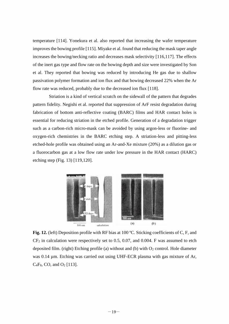
-19-
temperature [114]. Yonekura et al. also reported that increasing the wafer temperature
improves the bowing profile [115]. Miyake et al. found that reducing the mask taper angle
increases the bowing/necking ratio and decreases mask selectivity [116,117]. The effects
of the inert gas type and flow rate on the bowing depth and size were investigated by Son
et al. They reported that bowing was reduced by introducing He gas due to shallow
passivation polymer formation and ion flux and that bowing decreased 22% when the Ar
flow rate was reduced, probably due to the decreased ion flux [118].
Striation is a kind of vertical scratch on the sidewall of the pattern that degrades
pattern fidelity. Negishi et al. reported that suppression of ArF resist degradation during
fabrication of bottom anti-reflective coating (BARC) films and HAR contact holes is
essential for reducing striation in the etched profile. Generation of a degradation trigger
such as a carbon-rich micro-mask can be avoided by using argon-less or fluorine- and
oxygen-rich chemistries in the BARC etching step. A striation-less and pitting-less
etched-hole profile was obtained using an Ar-and-Xe mixture (20%) as a dilution gas or
a fluorocarbon gas at a low flow rate under low pressure in the HAR contact (HARC)
etching step (Fig. 13) [119,120].
Fig. 12. (left) Deposition profile with RF bias at 100 ºC. Sticking coefficients of C, F, and
CF2 in calculation were respectively set to 0.5, 0.07, and 0.004. F was assumed to etch
deposited film. (right) Etching profile (a) without and (b) with O2 control. Hole diameter
was 0.14 µm. Etching was carried out using UHF-ECR plasma with gas mixture of Ar,
C4F8, CO, and O2 [113].

-20-
Fig. 13. (left) Scanning electron microscopy (SEM) images of BARC and HAC(HARC)
profiles for different BARC processes: (a) pure CF4; (b) Ar/CF4. Typical HARC process
uses Ar/C4F6/O2/CO chemistry. (right) Top and side views of HARC etched profiles and
ashed profiles for various dilution gases: (a) Xe, (b) Ar-and-Xe (20%), (c) Ar, and (d) He.
ArF resist degradation during BARC and HARC etching step was reduced by controlling
BARC etched surface roughness and fluorocarbon polymers during HARC process [119].
Hole shape distortion and HAR hole twisting have been gaining attention as
serious problems. Huang et al. investigated profile distortion and shape twisting during
HAR oval contact etching [54]. Miyake et al. reported that asymmetric mask deformation
and asymmetric growth of the necking cause inequality of ion flux at the sidewalls,
resulting in twisting (Fig. 14) [116,117].
These phenomena are not yet fully understood: therefore, elucidation of the root
cause and research into controls are urgent issues. In addition, simulation technology has
been used to analyze the HAR etching process. Excellent results for modeling of oval
contact etching [121] and formation of facets and necking at masks [122,123] were
reported more than ten years ago, and the reliance on simulation technology has since
grown. This technology is expected to greatly contribute to the further development of
HAR etching in the future.

-21-
Fig. 14. (upper) Cross-sectional SEM images of initial tapered amorphous carbon layer
mask profiles and HARC etched profiles with diameter of 100 nm. (left) Atomic force
microscope image of 90-nm trench sidewall. Mask-edge roughness and non-uniformity
of necking affected bottom part of sidewall. (right) Calculated incident ion flux at
sidewall as a function of aspect ratio in hexagonal hole (tilt angle = 5 deg.).
1.4 Stacked multilayer etching
To overcome scaling limitations, the structure of NAND flash memories has
evolved from planar to 3D. In the 3D NAND flash architecture, memory cells are stacked

-22-
perpendicularly in an integrated device. 3D NAND devices such as bit-cost scalable
(BiCS) [124–126], vertical-gate NAND (VG-NAND) [127–129], and terabit-cell-array
transistor (TCAT) [130] ones reduce production costs per memory bit due to using a
single deep-etching process. These stacked devices are typically composed of alternating
layers of SiN (or polycrystalline-Si) and SiO2 [131–135].
In 3D NAND fabrication, it is difficult to form extremely HAR holes through
over 30 stacked film layers with both a vertical profile and high throughput. By using, for
example, a known technology, a cyclic process can be used in which etching SiO2 with
fluorocarbon-based gas is alternated with etching poly-Si with HBr gas [136–139].
However, this alternating process degrades throughput because additional time is needed
for the residual gases to be exhausted and the pressure to stabilize before the next etching
step. Thus, a single-step etching process under unique conditions could be a promising
technology for obtaining high throughput although this requires developing a novel
process and hardware. In a previous study, a one-piece etching reactor was developed that
can etch both poly-Si and SiO2 materials [140].
One of the problems with HAR etching of multiple layers is the decrease in the etching
rate as the aspect ratio of the holes/trenches increases. A dominant factor in this “etch-
rate drop” problem is the decrease in the density of the etchant, such as ions and radicals
with an increase in the aspect ratio. Several approaches have been investigated to suppress
the etch-rate drop [141]. One is to increase the ion energy to compensate for the decrease
in the ion flux. Another is to increase the plasma density to increase the flux of the ions
and radicals. A third is to reduce the sticking coefficient of the radicals to enhance the
transport of the radicals to the bottom of the holes/trenches. A fourth is to control the
deposition characteristics to increase the etching efficiency with ion bombardment.
1.5 Objectives of this study
This study focused on the development of an etching process for fabricating vertical
holes through different-material stacked films for 3D-NAND fabrication. A critical goal
was achieving both a vertical profile and high throughput for multiple-stack etching.
While the conventional process consists of multiple steps for each stacked layer, this
study investigated the use of HBr/fluorocarbon-based gas chemistry to achieve a single-

-23-
step etching process and thereby reduce processing time. The effects of wafer temperature
on the etching rate and surface composition were investigated to clarify the surface
reaction mechanism under HBr/N2/fluorocarbon-based gas plasma. The deposition
profile of a key material in the plasmas was investigated using macro cavities in order to
develop a model of the deposition material which indicates a mechanism of the material
to reach deeply.
1.6 Organization of this dissertation
This dissertation is organized as follows. Chapter 2 describes how a single-step
etching process was achieved by using HBr/N2/fluorocarbon-based gas plasma to create
a vertical hole profile in a poly-Si/SiO2 stack. Chapter 3 discusses the investigation of the
effects of wafer temperature on the etching rate and surface composition that clarified the
surface reaction mechanism under HBr/N2/fluorocarbon-based gas plasma. Chapter 4
discusses the investigation of the reaction mechanism during etching to fabricate deep
holes in SiN/SiO2 stacks by using a HBr/N2/fluorocarbon-based gas plasma. Chapter 5
describes the evaluation of the deposition profile of ammonium bromide in N2/HBr
plasmas as a function of the depth of a macro-cavity structure for HAR etching. Chapter
6 summarizes the key points of this dissertation.

-24-
References
[1] In Gartner report of “Market share analysis: Semiconductor worldwide, 2017”, (2018).
[2] S. Tachi, J. Vac. Sci. Technol. A 21, S131 (2003).
[3] H. Abe, M. Yoneda, and N. Fujiwara, Japan. J. Appl. Phys. 47, 1435 (2008).
[4] K. Eriguchi, Japan. J. Appl. Phys. 56, 06HA01 (2017).
[5] K. Ishikawa, K. Karahashi, T. Ichiki, J. P. Chang, S. M. George, W. M. M. Kessels, H. J. Lee, S.
Tinck, J. H. Um, and K. Kinoshita, Japan. J. Appl. Phys. 56, 06HA02 (2017).
[6] K. Ishikawa, K. Karahashi, T. Ishijima, S. I. Cho, S. Elliott, D. Hausmann, D. Mocuta, A. Wilson,
and K. Kinoshita, Japan. J. Appl. Phys. 57, 06JA01 (2018).
[7] M. J. Madou, “Pattern transfer with dry etching techniquies”, in “Fundamentals of
microfabrication: The science of miniaturization, 2nd ed.”, (CRC Press, 2002), p. 77.
[8] J. R. Hauser, “Introduction to semiconductor devices”, in “Handbook of Semiconductor
Manufacturing Technology, 2nd ed.”, ed. by Y. Nishi and R. Doering, (CRC Press, Florida USA,
2007), p. 1-2.
[9] R. A. Powell, “Reactive ion beam etching”, in “Dry etching for microelectronics”, ed. by P. A.
Powell (Elsevier, 1984), p. 115.
[10] N. Hosokawa, R. Matsuzaki, and T. Asamaki, Japan. J. Appl. Phys. 13, 435 (1974).
[11] S. Matsuo, Proceedings of 1st Dry Process Symposium (The Institute of Electrical Engineers of
Japan, Tokyo, 1979), p. 13.
[12] J. Coburn and H. Winters, J. Appl. Phys. 50, 3189 (1979).
[13] J. Coburn, Proceedings of 2nd Dry Process Symposium (The Institute of Electrical Engineers of
Japan, Tokyo, 1980), p. 103.
[14] A. von Keudell, and C. Corbella, J. Vac. Sci. Technol. A 35, 050801 (2017).
[15] M. Kumagawa, H. Sunami, T. Terasaki, and J. Nishizawa, Japan. J. Appl. Phys. 7, 1332 (1968).
[16] J. Nishizawa and N. Hayasaka, 157th Electrochem. Soc. Meeting, the plasma etching and
deposition symposium (1980).
[17] N. Abe, "Method and Apparatus for Dry Etching and Electrostatic Chucking Device used therein",
U.S. Pat. No. 4,384,918 May 24, 1983
[18] M. Nakamura, T. Kurimoto, H. Yano, and K. Yanagida, Proceedings of 9th Dry Process
Symposium (The Electrochemical Society USA, Hawaii, 1987), p. 1042.
[19] E. Ikawa, S. Sugito, and Y. Kurogi, Proceedings of 7th Dry Process Symposium (The Institute of
Electrical Engineers of Japan, Tokyo, 1985),
[20] N. Jiwari, H. Iwasawa, A. Nara, H. Sakaue, H. Sindo, T. Shoji, and Y. Horiike, Proceedings of
14th Dry Process Symposium (The Institute of Electrical Engineers of Japan, Tokyo, 1992), p. 23.
[21] K. Tsujimoto, T. Kumihashi, N. Kofuji, and S. Tachi, J. Vac. Sci. Technol. A 12, 1209 (1994).

-25-
[22] K. Harahuji, A. Yamano, and M. Kubota, Proceedings of 15th Dry Process Symposium (The
Institute of Electrical Engineers of Japan, Tokyo, 1993), p.11.
[23] K. Harafuji, A. Yamano, and M. Kubota, Japan. J. Appl. Phys. 33, 2212 (1995).
[24] H. Sugai, and Y Hikosaka, Proceedings of 14th Dry Process Symposium (The Institute of
Electrical Engineers of Japan, Tokyo, 1992) p.27.
[25] Y. Okamoto and H. Tamagawa, Japan. J. Appl. Phys. 11, 726 (1972).
[26] Y. Okamoto and H. Tamagawa, Rev. Sci. Inst. 43, 1193 (1972).
[27] N. Negishi, M. Izawa, K. Yokogawa, Y. Momonoi, T. Yoshida, K. Nakaune, H. Kawahara, M.
Kojima, K. Tsujimoto, and S. Tachi, Proceedings of 22nd Dry Process Symposium (The Institute
of Electrical Engineers of Japan, Tokyo, 2000), p. 31.
[28] K. Yokogawa, N. Itabashi, K. Suzuki, and S. Tachi, Electrochemical Society Series 97, Proc. the
symposium on silicon nitride and silicon dioxide thin insulating films, (Montreal, Canada, 1997), p.
493.
[29] J. Hopwood, Plasma Sources Sci. Technol. 1, 109 (1992).
[30] M. Sekine, M. Narita, S. Shimonishi, I. Sakai, K. Tomioka, K. Horioka, Y. Yoshida, and H.
Okano, Proceedings of 15th Dry Process Symposium (The Institute of Electrical Engineers of Japan,
Tokyo, 1993), p. 17.
[31] T. Kaminishizono, T. Akimoto, and E. Ikawa, Proceedings of 17th Dry Process Symposium (The
Institute of Electrical Engineers of Japan, Tokyo, 1995), p. 213.
[32] T. Akimoto, E. Ikawa, T. Sango, K. Komachi, K. Kitayama, and T. Ebata, Japan. J. Appl. Phys.
33, 7037 (1994).
[33] K. Yoshida, H. Miyamoto, E. Ikawa, and Y. Murao, Japan. J. Appl. Phys. 34, 2089 (1995).
[34] W. Tsai, G. Mueller, R. Lindquist, B. Frazier, and V. Vahedi, J. Vac. Sci. Technol. B 14, 3276
(1996).
[35] M. A. Liberman and A. J. Litchtenberg, “Principles of plasma discharges and material processing,
2nd ed.” (Wiley-interscience, New Jersey USA, 2005)
[36] P. Chabert and N. Braithwaite, “Physics of radio-frequency plasmas”, (Cambridge University
Press, Cambridge UK, 2011).
[37] M. Sekine, Appl. Surf. Sci. 192, 135 (2002).
[38] S. Morishita, H. Hayashi, T. Tatsumi, Y. Hikosaka, S. Noda, M. Okigawa, M. Matsui, M. Inoue,
and M. Sekine, Japan. J. Appl. Phys. 37, 6899 (1998)
[39] T. Tatsumi, Y. Hikosaka, S. Morishita, M. Matsui, and M. Sekine, J. Vac. Sci. Technol. A 17,
1562 (1999).
[40] H. Hayashi, M. Okigawa, S. Morishita, and M. Sekine, J. Vac. Sci. Technol. A 17, 2517 (1999).
[41] H. Hayashi, S. Morishita, T. Tatsumi, Y. Hikosaka, S. Noda, H. Nakagawa, S. Kobayashi, M.
Inoue, and T. Hoshino, J. Vac. Sci. Technol. A 17, 2557 (1999).

-26-
[42] T. Tatsumi, M. Matsui, M. Okigawa, and M. Sekine, J. Vac. Sci. Technol. B 18, 1897 (2000).
[43] M. Matsui, T. Tatsumi, and M. Sekine, J. Vac. Sci. Technol. A 19, 1282 (2001).
[44] M. Matsui, T. Tatsumi, and M. Sekine, J. Vac. Sci. Technol. A 19, 2089 (2001).
[45] H. Enomoto, K. Tago, N. Ohashi, and T. Tokunaga, Proceedings of 19th Dry Process Symposium
(The Institute of Electrical Engineers of Japan, Tokyo, 1997), p. 157.
[46] A. Takahashi, N. Ikegami, M. Kobayashi, and J. Kanamori, Proceedings of 20th Dry Process
Symposium (The Institute of Electrical Engineers of Japan, Tokyo, 1998), p. 251.
[47] Y. Ito, A. Koshiishi, R. Shimizu, M. Hagiwara, K. Inazawa, and E. Nishimura, Proceedings of
20th Dry Process Symposium (The Institute of Electrical Engineers of Japan, Tokyo, 1998), p. 263.
[48] O. Joubert, L. Vallier, P. Czuprynski, F. Vinet, P. Berruyer, and C. Verove, Proceedings of 20th
Dry Process Symposium (The Institute of Electrical Engineers of Japan, Tokyo, 1998), p. 241.
[49] H. Nakagawa, Y. Morikawa, E. Tamaoka, and T. Hayashi, Proceedings of 22nd Dry Process
Symposium (The Institute of Electrical Engineers of Japan, Tokyo, 2000), p. 257.
[50] T. Sakata, S. Komagata, S. Noda, N. Ikegami, M. Kobayashi, and J. Kanamori, Proceedings of
22nd Dry Process Symposium (The Institute of Electrical Engineers of Japan, Tokyo, 2000), p. 275.
[51] J. R. Han, Y. H. Liao, M. Chen, I. Huang, M. Hsieh, E. Chen, and M. Hiroshi, Proceedings of
30th Dry Process Symposium (Japanese Society of Applied Physics, Tokyo, 2008), p. 159.
[52] J. K. Kim, Y. J. Choi, S. -I. Cho, S. S. Jeong, S. W. Nam, C. -J. Kang, and T. H. Ahn, Proceedings
of 30th Dry Process Symposium (Japanese Society of Applied Physics, Tokyo, 2008), p. 271.
[53] C. G. Kim, D. S. Lee, B. H. Jeong, J. Yu, and W. J. Lee, Proceedings of 30th Dry Process
Symposium (Japanese Society of Applied Physics, Tokyo, 2008), p. 99.
[54] A. J. J. Huang, C. C. Min, J. K. Ma, Y. M. Tseng, W. J. Wang, C. M. Wu, C. C. Lin, and T. Y.
Huang, Proceedings of 28th Dry Process Symposium (Japanese Society of Applied Physics, Nagoya,
2006), p. 263.
[55] T. Iwase, M. Matsui, K. Yokogawa, T. Arase, and M. Mori, Proceedings of 37th Dry Process
Symposium (Japanese Society of Applied Physics, Awaji island, 2015), p. 47.
[56] T. Iwase, M. Matsui, K. Yokogawa, T. Arase, and M. Mori, Japan. J. Appl. Phys. 55, 06HB02
(2016).
[57] T. Iwase, K. Yokogawa, and M. Mori, Proceedings of 38th Dry Process Symposium (Japanese
Society of Applied Physics, Hokkaido, 2016), p. 197.
[58] T. Iwase, K. Yokogawa, and M. Mori, Japan. J. Appl. Phys. 56, 06HB04 (2017).
[59] T. Iwase, K. Yokogawa, and M. Mori, Proceedings of 39th Dry Process Symposium (Japanese
Society of Applied Physics, Tokyo, 2017), p. 209.
[60] T. Iwase, K. Yokogawa, and M. Mori, Japan. J. Appl. Phys. 57, 06JC03 (2018).
[61] R. A. Gottscho, C. W. Jurgensen, and D. J. Vitkavage, J. Vac. Sci. Technol. B 10, 2133 (1992).

-27-
[62] M. Oda, H. Namatsu, S. Ohki, H. Akiya, and T. Shibata, Proceedings of 6th Dry Process
Symposium (The Institute of Electrical Engineers of Japan, Tokyo, 1984), p. 115.
[63] S. Ohki, M. Oda, H. Akiya, and T. Shibata, J. Vac. Sci. Technol. B 5, 1611 (1987).
[64] H. Hayashi, T. Ohiwa, H. Tamura, M. Matsushita, I. Hasegawa, K. Horioka, and H. Okano,
Proceedings of 14th Dry Process Symposium (The Institute of Electrical Engineers of Japan, Tokyo,
1992), p. 205.
[65] H. Hayashi, K. Kurihara, and M. Sekine, Proceedings of 17th Dry Process Symposium (The
Institute of Electrical Engineers of Japan, Tokyo, 1995), p. 225.
[66] H. Hayashi, K. Kurihara, and M. Sekine, Japan. J. Appl. Phys. 35, 2488 (1996).
[67] S. Arai, N. Kofuji, K. Tsujimoto, and T. Mizutani, Proceedings of 16th Dry Process Symposium
(The Institute of Electrical Engineers of Japan, Tokyo, 1994), p. 223.
[68] N. Kofuji, K. Tsujimoto, T. Kumihashi, and T. Mizutani, Japan. J. Appl. Phys. 34, 2489 (1995).
[69] K. Shiozawa, K. Tabaru, T. Maruyama, N. Fujiwara, and M. Yoneda, Proceedings of 17th Dry
Process Symposium (The Institute of Electrical Engineers of Japan, Tokyo, 1995), p. 255.
[70] H. Kimura, K. Shiozawa, K. Kawai, H. Miyatake, and M. Yoneda, Japan. J. Appl. Phys. 34, 2114
(1995).
[71] N. Ikegami, A. Yabata, T. Matsui, J. Kanamori, and Y. Horiike, Proceedings of 18th Dry Process
Symposium (The Institute of Electrical Engineers of Japan, Tokyo, 1996), p. 147.
[72] N. Ikegami, A. Yabata, T. Matsui, J. Kanamori, and Y. Horiike, Japan. J. Appl. Phys. 36, 2470
(1997).
[73] K. Nishikawa, S. Tomohisa, H. Ootera, and T. Oomori, Proceedings of 19th Dry Process
Symposium (The Institute of Electrical Engineers of Japan, Tokyo, 1997), p. 145.
[74] K. Nishikawa, T. Oomori, and K. Ono, J. Vac. Sci. Technol. B 17, 127 (1999).
[75] A. Kojima, T. Ohiwa, M. Sekine, I. Sakai, S. Yonemoto, and Y. Watanabe, Proceedings of 19th
Dry Process Symposium (The Institute of Electrical Engineers of Japan, Tokyo, 1997), p. 151.
[76] T. Ohiwa, A. Kojima, M. Sekine, I. Sakai, S. Yonemoto, and Y. Watanabe, Japan. J. Appl. Phys.
37, 5060 (1998).
[77] M. Wang, A. Mosden, and M. J. Kushner, Proceedings of the 65th International Symposium of
the American Vacuum Society, (Long Beach, CA, October, 2018) PS+EM+SE-TuM6.
[78] K. Kurihara, M. Sekine, K. Horioka, and H. Okano, Proceedings of 16th Dry Process Symposium
(The Institute of Electrical Engineers of Japan, Tokyo, 1994), p. 217.
[79] K. Kurihara, and M. Sekine, Plasma Source, Sci. Technol. 5, 121 (1996).
[80] K. Kurihara, and M. Sekine, Japan. J. Appl. Phys. 39, 1369 (2000).
[81] G. Cunge, M. Darnon, J. Dubois, P. Bezard, O. Mourey, C. Petit-Etienne, L. Vallier, E. Despiau-
Pujo, and N. Sadeghi, Appl. Phys. Lett. 108, 093109 (2016).

-28-
[82] S. Noda, T. Kinoshita, Y. Hikosaka, N. Ozawa, H. Tsuboi, K. Kinoshita, and M. Sekine,
Proceedings of 21st Dry Process Symposium (The Institute of Electrical Engineers of Japan, Tokyo,
1999), p. 309.
[83] S. Noda, N. Ozawa, T. Kinoshita, H. Tsuboi, K. Kawashima, Y. Hikosaka, K. Kinoshita, and M.
Sekine, Thin Solid Film 374, 181 (2000).
[84] S. Kato, M, Sato, and Y. Arita, Proceedings of 11st Dry Process Symposium (The Institute of
Electrical Engineers of Japan, Tokyo, 1989), p. 33.
[85] M, Sato, S. Kato, and Y. Arita, Japan. J. Appl. Phys. 30, 1549 (1991).
[86] S. Kato, M, Sato, and Y. Arita, J. Vac. Sci. Technol. A 12, 1204 (1994).
[87] S. Sharma, D. Gahan, P. Scullin, S. Daniels, and M. B. Hopkins, Rev. Sci. Instrum. 86, 113501
(2015).
[88] H. Yabe, A. Yuuki, and Y. Matsui, Proceedings of 12th Dry Process Symposium (The Institute
of Electrical Engineers of Japan, Tokyo, 1990), p. 23.
[89] H. Yabe, A. Yuuki, and Y. Matsui, Japan. J. Appl. Phys. 30, 2873 (1991).
[90] Y. Gotoh, T. Kure, and S. Tachi, Proceedings of 14th Dry Process Symposium (The Institute of
Electrical Engineers of Japan, Tokyo, 1992), p. 199.
[91] Y. Gotoh, T. Kure, and S. Tachi, Japan. J. Appl. Phys. 32, 3035 (1993).
[92] Y. Gotoh, and T. Kure, Proceedings of 16th Dry Process Symposium (The Institute of Electrical
Engineers of Japan, Tokyo, 1994), p. 211.
[93] Y. Gotoh, and T. Kure, Japan. J. Appl. Phys. 34, 2132 (1995).
[94] K. Kubota, H. Matsumoto, H. Shindo, S. Shingubara, and Y. Horiike, Proceedings of 16th Dry
Process Symposium (The Institute of Electrical Engineers of Japan, Tokyo, 1994), p. 205.
[95] K. Kubota, H. Matsumoto, H. Shindo, S. Shingubara, and Y. Horiike, Japan. J. Appl. Phys. 34,
2119 (1995).
[96] T. Ono, R. Hamasaki, and T. Mizutani, Proceedings of 17th Dry Process Symposium (The
Institute of Electrical Engineers of Japan, Tokyo, 1995), p. 219.
[97] T. Ono, R. Hamasaki, and T. Mizutani, Japan. J. Appl. Phys. 33, L1717 (1994).
[98] T. Ono, R. Hamasaki, and T. Mizutani, Japan. J. Appl. Phys. 35, 2468 (1996).
[99] G-L. Liu, I. Aikawa, T. Koseki, N. Ikegami, H. Uchida, N. Hirashita, and J. Kanamori,
Proceedings of 19th Dry Process Symposium (The Institute of Electrical Engineers of Japan, Tokyo,
1997), p. 373.
[100] N. Ikegami, A. Yabata, G-L. Liu, H. Uchida, N. Hirashita, and J. Kanamori, Japan. J. Appl. Phys.
37, 2337 (1998).
[101] Y. Feurprier, M. Ogata, M. Ozawa, T. Kikuchi, Y. Chinzei, H. Shindo, T. Ichiki, and Y. Horiike,
Proceedings of 20th Dry Process Symposium (The Institute of Electrical Engineers of Japan, Tokyo,
1998), p. 9.

-29-
[102] Y. Feurprier, Y. Chinzei, M. Ogata, T. Kikuchi, M. Ozawa, T. Ichiki, and Y. Horiike, J. Vac.
Sci. Technol. A 17, 1556 (1999).
[103] N. Negishi, M. Miyake, K. Yokogawa, M. Oyama, T. Kanekiyo, and M. Izawa, J. Vac. Sci.
Technol. B, 35, 051205 (2017).
[104] K. Yonekura, S. Sakamori, T. Yokoi, N. Fujiwara, and H. Miyatake, Proceedings of 19th Dry
Process Symposium (The Institute of Electrical Engineers of Japan, Tokyo, 1997), p. 367.
[105] K. Yonekura,M. Kiritani, S. Sakamori, T. Yokoi, N. Fujiwara, and H. Miyatake, Japan. J. Appl.
Phys. 37, 2314 (1998).
[106] K. Yonekura, T. Katayama, T. Maruyama, N. Fujiwara, and H. Miyatake, Proceedings of 20th
Dry Process Symposium (The Institute of Electrical Engineers of Japan, Tokyo, 1998), p. 257.
[107] K. Yonekura, T. Katayama, T. Maruyama, N. Fujiwara, and H. Miyatake, J. Vac. Sci. Technol.
A 18, 176 (2000).
[108] S. Soda, T. Shinmura, M. Koyanagi, K. Hane, and S. Samukawa, Proceedings of 24th Dry
Process Symposium (The Institute of Electrical Engineers of Japan, Tokyo, 2002), p. 281.
[109] Y. Suzuki, T. Shinmura, M. Koyanagi, K. Hane, and S. Samukawa, Proceedings of 25th Dry
Process Symposium (The Institute of Electrical Engineers of Japan, Tokyo, 2003), p. 265.
[110] T. Shinmura, S. Soda, S. Samukawa, M. Koyanagi, and K. Hane, J. Vac. Sci. Technol. B 20,
2346 (2002).
[111] T. Shinmura, S. Soda, S. Samukawa, M. Koyanagi, and K. Hane, J. Vac. Sci. Technol. B 22,
533 (2002).
[112] T. Shinmura, Y. Suzuki, S. Soda, S. Samukawa, M. Koyanagi, and K. Hane, J. Vac. Sci. Technol.
A 22, 433 (2004).
[113] M. Izawa, K. Yokogawa, S. Yamamoto, N. Negishi, Y. Momonoi, K. Tsujimoto, and S. Tachi,
Proceedings of 21st Dry Process Symposium (The Institute of Electrical Engineers of Japan, Tokyo,
1999), p. 291.
[114] N. Negishi, M. Izawa, K. Yokogawa, Y. Momonoi, T. Yoshida, K. Nakaune, H. Kawahara, M.
Kojima, K. Tsujimoto, and S. Tachi, Proceedings of 22nd Dry Process Symposium (The Institute
of Electrical Engineers of Japan, Tokyo, 2000), p. 31.
[115] K. Yonekura, H. Matsuo, N. Fujiwara, and H. Miyatake, Proceedings of 23rd Dry Process
Symposium (The Institute of Electrical Engineers of Japan, Tokyo, 2001), p. 285.
[116] M. Miyake, N. Negishi, M. Izawa, K. Yokogawa, M. Oyama, and T. Kanekiyo, Proceedings of
30th Dry Process Symposium (Japanese Society of Applied Physics, Tokyo, 2008), p. 275.
[117] M. Miyake, N. Negishi, M. Izawa, K. Yokogawa, M. Oyama, and T. Kanekiyo, Japan. J. Appl.
Phys. 48, 08HE01 (2009).
[118] S. Y. Son, C. H. Shin, Y. J. Kim, G. J. Min, C. J. Kang, and H. K. Cho, Proceedings of 26th Dry
Process Symposium (The Institute of Electrical Engineers of Japan, Tokyo, 2004), p. 77.

-30-
[119] N. Negishi, H. Takesue, M. Sumiya, T. Yoshida, and M. Izawa, Proceedings of 25th Dry Process
Symposium (The Institute of Electrical Engineers of Japan, Tokyo, 2003), p. 287.
[120] N. Negishi, H. Takesue, M. Sumiya, T. Yoshida, Y. Momonoi, and M. Izawa, J. Vac. Sci.
Technol. B 23, 217 (2005).
[121] S. C. Park, S. Lim, C. H. Shin, G. J. Min, C. J. Kang, H. K. Cho, and J. T. Moon, Proceedings
of 27th Dry Process Symposium (Japanese Society of Applied Physics, Jeju Korea, 2005), p. 5.
[122] D. Kim, E. Hudson, D. Cooperberg, E. Edelberg, and M. Srinivasan, Proceedings of 27th Dry
Process Symposium (Japanese Society of Applied Physics, Jeju Korea, 2005), p. 241.
[123] D. Kim, E. Hudson, D. Cooperberg, E. Edelberg, and M. Srinivasan, Thin Solid Film 515, 4874
(2007).
[124] H. Tanaka, M. Kido, K. Yahashi, M. Oomura, R. Katsumata, M. Kito, Y. Fukuzumi, M. Sato,
Y. Nagata, Y. Matsuoka, Y. Iwata, H. Aochi, and A. Nitayama, Symp. VLSI Technol. Dig. Tech.
Pap., 2007, p. 14.
[125] Y. Fukuzumi, R. Katsumata, M. Kito, M. Kido, M. Sato, H. Tanaka, Y. Nagata, Y. Matsuoka,
Y. Iwata, H. Aochi, and A. Nitayama, IEDM Tech. Dig., 2007, p. 449.
[126] R. Katsumata, M. Kito, Y. Fukuzumi, M. Kido, H. Tanaka, Y. Komori, M. Ishiduki, J.
Matsunami, T. Fujiwara, Y. Nagata, Z. Li, Y. Iwata, R. Kirisawa, H. Aochi, and A. Nitayama, Symp.
VLSI Technol. Dig. Tech. Pap., 2009, p. 136.
[127] W. Kim, S. Choi, J. Sung, T. Lee, C. Park, H. Ko, J. Jung, I. Yoo, and Y. Park, Symp. VLSI
Technol. Dig. Tech. Pap., 2009, p. 188.
[128] H.-T. Lue, T.-H. Hsu, Y.-H. Hsiao, S. P. Hong, M. T. Wu, F. H. Hsu, N. Z. Lien, S.-Y. Wang,
J.-Y. Hsieh, L.-W. Yang, T. Yang, K.-C. Chen, K.-Y. Hsieh, and C.-Y. Lu, Symp. VLSI Technol.
Dig. Tech. Pap., 2010, p. 131.
[129] C.-P. Chen, H.-T. Lue, K.-P. Chang, Y.-H. Hsiao, C.-C. Hsieh, S.-H. Chen, Y.-H. Shih, K.-Y.
Hsieh, T. Yang, K.-C. Chen, and C.-Y. Lu, Symp. VLSI Technol. Dig. Tech. Pap., 2012, p. 91.
[130] J. Jang, H. Kim, W. Cho, H. Cho, J. Kim, S. I. Shim, Y. Jang, J. Jeong, B. Son, D. W. Kim, K.
Kim, J. Shim, J. S. Lim, K. Kim, S. Y. Yi, J. Lim, D. Chung, H. Moon, S. Hwang, J. Lee, Y. Son,
U. Chung, and W. Lee, Symp. on VLSI Technol. Tech. Dig., pp. 192-193 (2009).
[131] S. Whang, K. Lee, D. Shin, B. Kim, M. Kim, J. Bin, J. Han, S. Kim, B. Lee, Y. Jung, S. Cho, C.
Shin, H. Yoo, S. Choi, K. Hong, S. Aritome, S. Park, and S. Hong, IEDM Tech. Dig., 2010, p. 668.
[132] S. H. Chen, H. T. Lue, Y. H. Shih, C. F. Chen, T. H. Hsu, Y. R. Chen, Y. H. Hsiao, S. C. Huang,
K. P. Chang, C. C. Hsieh, G. R. Lee, A. T. H. Chuang, C. W. Hu, C. J. Chiu, L. Y. Lin, H. J. Lee,
F. N. Tsai, C. C. Yang, T. Yang, and C. Y. Lu, IEDM Tech. Dig., 2012, p. 21.
[133] A. Goda and K. Parat, IEDM Tech. Dig., 2012, p. 13.
[134] H. Lue, T. Hsu, C. Wu, W. Chen, T. Yeh, K. Chang, C. Hsieh, P. Du, Y. Hsiao, Y. Jiang, G.
Lee, R. Lo, Y. Su, C. Huang, S. Lai, L. Liang, C. Chen, M. Hung, C. Hu, C. Chiu, and C. Lu, IEDM

-31-
Tech. Dig., 2015, p. 44.
[135] K. Parat and C. Dennison, IEDM Tech. Dig., 2015, p. 48.
[136] M. A. Vyvoda, H. Lee, M. V. Malyshev, F. P. Klemens, M. Cerullo, V. M. Donnelly, D. B.
Graves, A. Kornblit, and J. T. C. Lee, J. Vac. Sci. Technol. A 16 [6], 3247 (1998).
[137] N. R. Rueger, J. J. Beulens, M. Schaepkens, M. F. Doemling, J. M. Mirza, T. E. F. M. Standaert,
and G. S. Oehrlein, J. Vac. Sci. Technol. A 15 [4], 1881 (1997).
[138] D. R. Sparks, J. Electrochem. Soc. 139 [6], 1736 (1992).
[139] Z. Yang, F. H. Hsu, L. Y. Lin, H. J. Lee, N. T. Lian, T. Yang, K. C. Chen, and C. Y. Lu,
Advanced Semiconductor Manufacturing Conf. (ASMC), 2013, p. 24.
[140] T. Iwase, K. Yokogawa, T. Arase, A. Hirata, M. Mori, Symp. on SPIE Advanced Lithography
Technical Summary, 2015, p. 160.
[141] C. M. Huard et al., J. Vac. Sci. Technol. A 35 (5), 05C301 (2017).

-32-
2. Demonstration of High-Aspect-Ratio Multilayer Etching in
HBr/CH3F-based Gas Plasmas with N2 Gas Addition
2.1 Introduction
The integration of semiconductor devices for the next-generation nodes of logic and
memory presents enormous challenges for etching; current planar flash memory devices
in particular face critical scaling limitations.1-3) Three-dimensional (3D) NAND device
fabrication has been improved in manufacturing fabs for the flash memory market by
perpendicular integration.4-8) A 3D NAND device structure was realized by fabricating
holes in stacked layers in which polycrystalline silicon (poly-Si) forming electrodes and
a SiO2 insulator were alternately deposited.9-14)
In 3D NAND fabrication, it is difficult to form extremely high-aspect-ratio holes
through over 30 stacked film layers with both a vertical profile and high throughput. By
using, for example, a known technology, we can apply a cyclic process in which etching
SiO2 with fluorocarbon-based gas is alternated with etching poly-Si with HBr gas.15-18)
However, this alternating process has a disadvantage in terms of throughput because a
multiple-step process needs additional time for residual gases to be exhausted and for
pressure to stabilize before the next etching step. Thus, a single-step etching process under
unique conditions could be a promising technology for obtaining a high throughput,
although a novel process and hardware must be developed in the future to fully realize
this process. In our previous study, one piece of hardware, an etching reactor that can etch
both poly-Si and SiO2 materials, was developed.19)
In this paper, we report on the development of an etching process for fabricating
vertical holes through poly-Si/SiO2 stacks for 3D-NAND technology. A gas mixture of
HBr and fluorocarbon was used for obtaining quite similar poly-Si and SiO2 etching rates
to realize a single-step etching process. The material composition on the surface was
estimated using a simulation program to investigate gas chemistry. The composition was
also analyzed by XPS to confirm the simulation results. Finally, the obtained etching
profile was evaluated to reveal the etching process.

-33-
2.2 Experimental procedure
Stacked films with a hole pattern were fabricated for profile evaluation. Figure 1
shows a cross-sectional SEM image and a schematic image of a sample for profile
evaluation. Eight pairs of 50-nm-thick poly-Si and SiO2 layers were alternately deposited
on a Si substrate. An 800-nm-thick amorphous carbon layer (ACL) was deposited as an
etching mask on the poly-Si/SiO2 stacks, and 50-nm-thick SiON was deposited as a mask
for the 800-nm-thick ACL. 50-nm-diameter holes were patterned in a 120-nm-thick resist
film coated on the SiON layer by the electron beam lithography method.
Fig. 1. (a) Cross-sectional SEM image, (b) schematic image of etching profile evaluation
sample.
The stacked film samples were processed using a parallel-plate etching reactor
supplied with 200 MHz VHF power to generate HBr/fluorocarbon-based gas plasma.
Chamber wall sputtering and plasma diffusion can be suppressed by a 200 MHz discharge
effect.20, 21) Figure 2 shows a schematic of the reactor. The gas inlet under the upper
electrode in the reactor was made of a dielectric material that can withstand a corrosive
gas. The VHF source power and wafer bias power were applied at 1000 and 1200 W,
respectively. The process pressure was controlled at 6.0 Pa. The wafer temperature was
controlled on an electrostatic chuck stage between 10 to 60°C using a circulator system.
The sample for profile evaluation were divided into 20-mm-square pieces and pasted with
grease on 300 mm wafers coated with a photoresist (PR). In an ancillary experiment, PR
EB resist
SiON
ACL
SiO2Poly-SiSiO2
Poly-Si
Si-substrate
・・・
800 nm
850 nm
50 nm50 nm
50 nm
(a) (b)
300 nm

-34-
was selected as the base wafer for coupon evaluation in terms of etching rate and profile.
The carbon by-product during ACL mask etching might be similar to carbon in PR.
Fig. 2. Schematic of parallel-plate etching reactor. The reactor has a 200 MHz VHF
plasma source and a 4 MHz wafer bias generator. The gas inlet in the upper electrode is
made of a dielectric material that withstands corrosive gas.
For processing, cross-sectional images were obtained by field-emission SEM (Hitachi
S-5200). Etching rate was evaluated using blanket wafers deposited with poly-Si, SiO2,
or PR. Film thickness was measured using an optical film-thickness meter (Nanometrics
Nanospec 6100). The composition of the sample surface was analyzed by XPS. 20-mm-
square coupons of poly-Si, SiO2, and PR were pasted on the PR-coated 300 mm wafers.
These samples were processed in the reactor under the same conditions as the profile
evaluation ones. The surface composition was estimated by peak deconvolution of XPS
spectra.
The equilibrium composition was simulated using the software “HSC chemistry”
(HSC) made by Outotec Research Oy. to investigate the possible materials produced
when several gas species were mixed. HSC can calculate the composition of equilibrium
state materials by the Gibbs energy minimization method. The following were the initial
conditions: pressure, 6 Pa; temperature, 25°C; and mol numbers of HBr and fluorocarbon,
13 and 19 kmol, respectively. Note that there were ions and radicals besides gas molecules
in the etching reactor because part of the mixture of gases was discharged at the 200 MHz
VHF power. Therefore, HSC might not completely simulate an actual situation; however,
the HSC results could be used to determine the materials that tended to be generated.
4-MHz bias power source
200-MHz power sourceCoil
Process gas inlet
Exhaust
Plasma
GND
Wafer stage
Lower electrode
Upper electrode

-35-
2.3 Results and discussion
2.3.1 Gas mixing for continuous etching process
Figure 3 shows the dependence of the poly-Si and SiO2 etching rates (ERs) on the
HBr to fluorocarbon gas mixing ratio at a wafer temperature of 60°C. The total gas-flow
rate was set to be constant at 300 ml/min. Poly-Si ER increased when the HBr ratio was
high, and SiO2 ER increased when the fluorocarbon ratio was high because fluorocarbon
radicals might have impeded the etching of poly-Si. This result indicates that the ERs of
poly-Si and SiO2 can be made almost equal when the HBr ratio is 0.40.
Fig. 3. Dependence of poly-Si and SiO2 etching rates on HBr and fluorocarbon gas mixing
ratio. (a) and (b) indicate HBr mixing ratios of 0.67 and 0.40, respectively.
Next, the relationship between the etching profile of the poly-Si/SiO2 stacks and the
poly-Si and SiO2 ERs was investigated (shown in Fig. 4). When an HBr ratio of 0.67 was
applied, side etching progressed in the poly-Si layer because the poly-Si ER is higher than
that of SiO2. However, a smooth side wall was obtained when an HBr ratio of 0.40 was
applied, but the bottom profile was tapered. The tapering might have been caused by
excessive amount of carbon(C)-based polymers sticking onto the side wall, which inhibits
spontaneous etching because HBr/fluorocarbon plasma could have generated a CxFy
and/or CzHu (here, x, y, z, u are integers) polymer. Generally, the sticking of C-based
polymers is controlled by addiing O2 gas for high-aspect-ratio-contact (HARC) etching,
but O2 addition decreases the etching selectivity of an ACL mask. According to previous
studies, if a C-based polymer formed CxNyFzHu by combining with nitrogen (N) and
0
100
200
300
400
0 0.2 0.4 0.6 0.8 1
Etc
hin
g R
ate
(n
m/m
in)
HBr/(HBr + fluorocarbon)
Poly-Si
SiO2
(a)
(b)

-36-
hydrogen (H), a carbon on a surface can be easily removed by high volatility of by-
product, e.g. HCN.22, 23) A vertical profile may be obtained by bottom etching progression
without side etching progression because the sticking CxNyFzHu polymer may act as a
protective film.
Fig. 4. Schematic of cross-sectional etching profile. Holes were fabricated in poly-Si/SiO2
stacks when the (a) HBr mixing ratios were 0.67 (b) and 0.40.
2.3.2 Equilibrium simulation with additional gas
We simulated chemical equilibrium by using HSC to determine a combination of N
and H that would result in their stable existence on the surface by gas addition. It was
found that N2 gas addition may result in the generation of an ammonium salt. Figure 5
shows the simulation result for the N2 gas amount dependence on material concentration
at a temperature of 25C. The concentration of ammonium bromine (NH4Br) increased
as HBr and methane (CH4) decreased after N2 flow addition. It is promising that N and H
existed stably on the surface because ammonium bromine is solid at room temperature.
Figure 6 shows the simulation result for the temperature dependence on material
concentration with N2 addition. The figure shows that ammonium bromine tended to be
produced at a low temperature. The concentration of ammonium bromine decreased as
the temperature increased, while a steady state existed at approximately 20 to 50C.
ACL
Poly-Si
SiO2
(a) HBr ratio: 0.67 (b) HBr ratio: 0.40
Si sub.

-37-
Fig. 5. N2 gas amount dependence on material amount calculated by chemical equilibrium
simulation. The temperature was 25C and the pressure was 6.0 Pa. (g) and (s) indicate
vapor phase and solid phase, respectively.
Fig. 6. Temperature dependence on material amount with N2 addition calculated by
chemical equilibrium simulation. (g) and (s) indicate the vapor phase and solid phase,
respectively.
2.3.3 Surface composition dependence on-wafer temperature
The surface compositions of the by-products or a mixing layer processed at a high
wafer temperature of 60C and a low wafer temperature of 20C were examined by XPS
analysis. First, the samples were processed without applying a wafer bias to separate
molecular or radical adsorption from ion-assisted reaction. XPS narrow scan spectra of N
1s and Br 3d peaks were measured to determine the chemical bonding of elements on the
surface.
N2 Amount [mol]
Ma
teri
al A
mo
un
t [m
ol]
Temperature [C]
Ma
teri
al A
mo
un
t [m
ol]

-38-
Figure 7 shows the relationship between wafer temperature and XPS spectra. N 1s
spectra were deconvoluted into two contributions, one due to N-C nitrogen (detected at
399.8 eV) and the other to N-H nitrogen (detected at 401.3 eV).24, 25) Br 3d spectra were
deconvoluted into two contributions, one due to Br or Br- bromine (detected at 68.8 eV)
and the other to Br-C bromine (detected at 70.5 eV).26) The intensity of the Br or Br- peaks
and N-H peak increased at the low wafer temperature of 20°C. By comparing between
results of the chemical equilibrium simulation and the XPS analysis without wafer bias,
we found that these results corresponded roughly. It is reasonable to suppose that the
concentrations of N-H and Br on the surface at a low wafer temperature were caused by
the formation of ammonium bromine. Therefore, these results indicate that N, H, and Br
can exist stably on the surface at a low wafer temperature.
Fig. 7. XPS narrow scan using poly-Si sample without applying wafer bias. (a) N 1s peak
at wafer temperature of 60C, (b) Br 3d peak at 60C, (c) N 1s peak at 20C, and (d) Br
3d peak at 20C. These spectra were deconvoluted (shown as black solid curved line).
390395400405410
Inte
nsi
ty (a. u.)
Binding Energy (eV)
N1s
N-C
N-H
6065707580
Inte
nsity (a. u.)
Binding Energy (eV)
Br3d
390395400405410
Inte
nsi
ty (a. u.)
Binding Energy (eV)
N1s
N-H N-C BrBr-C
6065707580
Inte
nsi
ty (a. u
.)
Binding Energy (eV)
Br3d
BrBr-C
(a) (b)
(c) (d)
Inte
nsity (a
rb. u
nit)
Inte
nsity (a
rb. u
nit)
Inte
nsity (a
rb. u
nit)
Inte
nsity (a
rb. u
nit)

-39-
Next, high-energy ions were irradiated by applying a wafer bias to confirm whether
N, H, and Br are volatilized by chemical reaction on the surface. Figure 8 shows the XPS
spectra of N 1s and Br 3d peaks when a wafer bias was applied at a wafer temperature of
20°C. The Br and N-H peaks almost disappeared when high-energy ions were irradiated.
Here, the C-based polymer thicknesses at wafer temperatures of 20 and 60°C, which were
estimated from the C 1s peak intensity of the XPS spectra, were 2.2 and 2.5 nm,
respectively. Therefore, N, H, and Br might have been volatilized with the C-based
polymer by high-energy-ion irradiation.
Fig. 8. XPS narrow scan using poly-Si sample with wafer bias applied. (a) N 1s peak, (b)
Br 3d peak at wafer temperature of 20C. These spectra were deconvoluted (shown as
black solid curved line).
2.3.4 Etching profile evaluation
We evaluated the etching profiles of the poly-Si/SiO2 stacks at several wafer
temperatures by equilibrium simulation and surface composition analysis. Figure 9 shows
cross-sectional SEM images demonstrating the wafer temperature dependence on the
etching profile of the stacks. The stacks were etched by N2/HBr/fluorocarbon plasma
through an ACL hole mask. When a wafer temperature of 60°C and 300 s of processing
time were applied, the bottom profile of the holes was tapered because there was a large
amount of the C-based polymer sticking. However, when a wafer temperature of 20°C
and 300 s of processing time were applied, the etching rate was increased owing to the C-
based polymer being reduced by existing N, H, and Br. Furthermore, the hole bottom
profile differed depending on the wafer temperature; the profile at 20°C showed a flat
6065707580
Inte
nsi
ty (a. u.)
Binding Energy (eV)
Br3d
390395400405410
Inte
nsi
ty (a. u.)
Binding Energy (eV)
N1s
N-C
BrBr-C
(a) (b)
Inte
nsity (a
rb. u
nit)
Inte
nsity (a
rb. u
nit)

-40-
bottom, and that at 60°C showed a tapered bottom. By adjusting the wafer temperature to
10°C and processing time to 400 s, a 1.2-m-depth vertical hole profile with an aspect
ratio of 24 was obtained.
Fig. 9. Cross-sectional SEM image of poly-Si/SiO2 stack etching profile. (a) 300 s of
etching at wafer temperature of 60C, (b) 300 s of etching at 20C, (c) 400 s of etching at
10C.
2.3.5 Modeling a surface reaction
Anisotropic etching of Si in halogen gas plasma can be realized at a decreased wafer
temperature owing to the decreased by-product reactivity on the sidewall.27-29) “Necking”
and “bowing” due to SiO2 etching under fluorocarbon-based gas plasma can be improved
with an increased wafer temperature owing to the optimized carbon sticking.30)
Conversely, it was found that there was a quite different temperature dependence between
typical SiO2 etching and poly-Si/SiO2 etching with N2-added HBr/fluorocarbon plasma.
A surface reaction model that depends on the wafer temperature was examined
considering the surface composition of by-products or mixing layers. At a high wafer
temperature of 60°C, it is assumed that a C-based material (by-product or polymer) was
deposited in the etched holes because fluorocarbon/HBr plasma and Si generate C-based
materials of a low vapor pressure, such as CHx, CFx, CBrx, and SiCx. The deposited
200 nm
1.2 μm
50 nm
200 nm200 nm
Aspect ratio = 24S
i-s
ub
str
ate
Po
ly-S
i/S
iO2
sta
ck
sA
CL
ma
sk
(a) (b) (c)

-41-
carbon might have formed a protective layer at the sidewall and caused the tapering of
the bottom. In contrast, at a low wafer temperature of 20°C, N-H and Br existed on the Si
surface, as shown in Fig. 7. It is considered that N-H and Br are present in the deposition
layer. N-H could have volatilized excessive amount of carbon in the deposition layer that
changed to hydrogen cyanide or carbon nitride. Br contained in the deposition layer could
have enhanced the etching of Si. The deposited carbon on the sidewall may form a thin
protective layer since the sidewall is also exposed by ion irradiation; therefore, it is
considered that the vertical profile has been improved. The chemical reaction between Si
and Br may not proceed efficiently without a high-energy-ion impact because the
activation energy of SiBr4 is higher than that of carbon nitride. The chemical reaction
between Si and Br contained in the deposition layer might not proceed efficiently in the
sidewall because a low incident-angle ion provides less energy. Conversely, the chemical
reactions of Si-Br and C-N might have been enhanced in the hole bottom by a high
incident-angle ion; therefore, it is considered that etching rate has been increased. The
surface reaction model can explain the temperature dependence on the etching profile. It
is reasonable to suppose that the vertical profile is obtained by the formation of a reactive
surface reaction layer that contains N, H, and Br at a low wafer temperature.
2.4 Conclusion
We investigated the effect of wafer temperature on the etching profile of high-aspect-
ratio holes in poly-Si/SiO2 stacks by analyzing surface reaction layers. HBr/
fluorocarbon-based gas plasma was used to achieve a single-step etching process to
improve the throughput of the process. XPS results revealed that the N-H and Br
adsorption on the surface was enhanced at a low wafer temperature of 20°C, which results
in a reduced thickness of the C-based layer because N-H enhances the generation of the
HCN by-product. The stability of NH4Br at a lower temperature was also examined by
chemical equilibrium simulation. Finally, vertical holes with an aspect ratio of 24 were
obtained at a wafer temperature of 10°C using this single-step process.

-42-
References
[1] S. Bangsaruntip, G. M. Cohen, A. Majumdar, Y. Zhang, S. U. Engelmann, N. C. M. Fuller, L. M.
Gignac, S. Mittal, J. S. Newbury, M. Guillorn, T. Barwicz, L. Sekaric, M. M. Frank, and J. W.
Sleight, IEDM Tech. Dig., 2009, p. 297.
[2] A. Veloso, S. Demuynck, M. Ercken, A. M. Goethals, S. Locorotondo, F. Lazzarino, E.
Altamirano, C. Huffman, C. Delvaux, B. Baudemprez, T. Vandeweyer, F. Van Roey, C. Baerts, D.
Goossens, H. Dekkers, P. Ong, N. Heylen, K. Kellens, H. Volders, A. Hikavyy, C. Vrancken, M.
Rakowski, S. Verhaegen, M. Dusa, L. Romijn, C. Pigneret, A. Van Dijk, R. Schreutelkamp, A.
Cockburn, V. Gravey, H. Meiling, B. Hultermans, S. Lok, K. Shah, R. Rajagopalan, J. Gelatos, O.
Richard, H. Bender, G. Vandenberghe, G. P. Beyer, P. Absil, T. Hoffmann, K. Ronse, and S.
Biesemans, IEDM Tech. Dig. , 2009, p. 301.
[3] A. Veloso, A. De Keersgieter, S. Brus, N. Horiguchi, P. P. Absil, and T. Hoffmann, Jpn. J. Appl.
Phys. 50, 04DC16 (2011).
[4] H. Tanaka, M. Kido, K. Yahashi, M. Oomura, R. Katsumata, M. Kito, Y. Fukuzumi, M. Sato, Y.
Nagata, Y. Matsuoka, Y. Iwata, H. Aochi, and A. Nitayama, Symp. on VLSI Technology Digest of
Technical Papers, 2007, p. 14.
[5] R. Katsumata, M. Kito, Y. Fukuzumi, M. Kido, H. Tanaka, Y. Komori, M. Ishiduki, J.
Matsunami, T. Fujiwara, Y. Nagata, Z. Li, Y. Iwata, R. Kirisawa, H. Aochi, and A. Nitayama, Proc.
Symp. VLSI Technol., 2009, p. 136.
[6] Y. Kim, J.-G. Yun, S. H. Park, W. Kim, J. Y. Seo, M. Kang, K.-C. Ryoo, J.-H. Oh, J.-H. Lee, H.
Shin, and B.-G. Park, IEEE Trans. Electron Devices 59 [1], 35 (2011).
[7] E. Choi and S. Park, IEDM Tech. Dig., pp. 211-214 (2012).
[8] Y. Hsiao, H. Lue, W. Chen, B. Tsui, K. Hsieh, and C. Lu, IEEE Electron Devices Lett. 36 [10],
1015 (2015).
[9] H. T. Lue, T. H. Hsu, Y. H. Hsiao, S. P. Hong, M. T. Wu, F. H. Hsu, N. Z. Lien, S. Y. Wang, J. Y.
Hsieh, L. W. Yang, T. Yang, K. C. Chen, K. Y. Hsieh, and C. Y. Lu, Symp. on VLSI Technology
Digest of Technical Papers, 2010, p. 131.
[10] S. Whang, K. Lee, D. Shin, B. Kim, M. Kim, J. Bin, J. Han, S. Kim, B. Lee, Y. Jung, S. Cho, C.
Shin, H. Yoo, S. Choi, K. Hong, S. Aritome, S. Park, and S. Hong, IEDM Tech. Dig., 2010, p. 668.
[11] S. H. Chen, H. T. Lue, Y. H. Shih, C. F. Chen, T. H. Hsu, Y. R. Chen, Y. H. Hsiao, S. C. Huang,
K. P. Chang, C. C. Hsieh, G. R. Lee, A. T. H. Chuang, C. W. Hu, C. J. Chiu, L. Y. Lin, H. J. Lee, F.
N. Tsai, C. C. Yang, T. Yang, and C. Y. Lu, IEDM Tech. Dig., 2012, p. 21.
[12] A. Goda and K. Parat, IEDM Tech. Dig., 2012, p. 13.
[13] H. Lue, T. Hsu, C. Wu, W. Chen, T. Yeh, K. Chang, C. Hsieh, P. Du, Y. Hsiao, Y. Jiang, G. Lee,
R. Lo, Y. Su, C. Huang, S. Lai, L. Liang, C. Chen, M. Hung, C. Hu, C. Chiu, and C. Lu, IEDM
Tech. Dig., 2015, p. 44.
-43-
[14] K. Parat and C. Dennison, IEDM Tech. Dig., 2015, p. 48.
[15] M. A. Vyvoda, H. Lee, M. V. Malyshev, F. P. Klemens, M. Cerullo, V. M. Donnelly, D. B.
Graves, A. Kornblit, and J. T. C. Lee, J. Vac. Sci. Technol. A 16 [6], 3247 (1998).
[16] N. R. Rueger, J. J. Beulens, M. Schaepkens, M. F. Doemling, J. M. Mirza, T. E. F. M. Standaert,
and G. S. Oehrlein, J. Vac. Sci. Technol. A 15 [4], 1881 (1997).
[17] D. R. Sparks, J. Electrochem. Soc. 139 [6], 1736 (1992).
[18] Z. Yang, F. H. Hsu, L. Y. Lin, H. J. Lee, N. T. Lian, T. Yang, K. C. Chen, and C. Y. Lu,
Advanced Semiconductor Manufacturing Conf. (ASMC), 2013, p. 24.
[19] T. Iwase, K. Yokogawa, T. Arase, A. Hirata, M. Mori, Symp. on SPIE Advanced Lithography
Technical Summary, 2015, p. 160.
[20] K. Yokogawa, K. Maeda, H. Kobayashi, T. Kanekiyo, and M. Izawa, Proc. 7th Int. Conf.
Microelectronics and Interfaces, 2006.
[21] K. Yokogawa, K. Maeda, and M. Izawa, Jpn. J. Appl. Phys. 47, 6854 (2008).
[22] H. Nagai, S. Takashima, M. Hiramatsu, M. Hori, and T. Goto, J. Appl. Phys. 91, 2615 (2002).
[23] M. Ooka and S. Yokoyama, Jpn. J. Appl. Phys. 44, 6476 (2005).
[24] K. Ogata, J. Fernando D. Chubaci, and F. Fujimoto, J. Appl. Phys. 76, 3791 (1994).
[25] S. Bourbigot, M. Le Bras, L. Gengembre, and R. Delobel, Applied Surface Science 81, 299
(1994).
[26] AC Brieva, C Jäger, F Huisken, L Šiller, and YV Butenko, Carbon 47, 2812 (2009).
[27] S. Tachi, K. Tsujimoto, S. Arai, and T. Kure, J. Vac. Sci. Technol. A 9, 796 (1991).
[28] M. Haverlag, G. S. Oehrlein, and D. Vender, J. Vac. Sci. Technol. B 12, 96 (1994).
[29] B. Wu, A. Kumar, and S. Pamarthy, J. Appl. Phys. 108, 051101 (2010).
[30] H. Abe, M. Yoneda, and N. Fujiwara, Jpn. J. Appl. Phys. 47, 1435 (2008).

-44-
3. Effect of Temperature on Composition of Deposition Layer
in HBr/N2/CH3F-based Gas Plasmas
3.1 Introduction
Semiconductor device architecture has been changing from being planar to being
three-dimensional (3D) because the integration of semiconductor devices has faced a
scaling limitation. 3D NAND flash architecture stacks memory cells in an integrated
device perpendicularly. Such devices as bit-cost scalable (BiCS) 1-3) and vertical-gate
NAND (VG-NAND) 4-6) structures can reduce production costs per memory bit. A 3D
NAND flash structure can be achieved by fabricating holes in stacked layers in which
polycrystalline silicon (poly-Si) forming electrodes and silicon dioxide (SiO2) insulators
are alternately deposited.7-11) In the 3D NAND fabrication process, holes with extremely
high aspect ratio (> 50) are fabricated through more than 30 stacked film layers with both
a high throughput and a vertical profile. A cyclic process, for example, can be used for
stacked layer etching, in which etching SiO2 with fluorocarbon-based gas is alternately
performed with etching poly-Si with HBr gas.12-15) However, this process has a
disadvantage in terms of throughput because it requires an additional time to exhaust
residual gases and stabilize the pressure before the next etching step. Thus, a single-step
etching process under unique conditions could be a promising technology for obtaining a
high throughput.
Our previous work demonstrated that a single-step etching process could be
achieved by using HBr/N2/fluorocarbon-based gas plasma to create a vertical hole profile
in a poly-Si/SiO2 stack.16, 17) HBr and fluorocarbon gas were mixed to uniform etching
rates of both poly-Si and SiO2 to obtain smooth side walls in the holes.14, 18-21)
Furthermore, nitrogen gas was added and the wafer temperature was adjusted to obtain
the vertical hole profile. However, a surface reaction mechanism under
HBr/N2/fluorocarbon-based gas plasma has not been investigated yet. A deposition film
consisting of a fluorocarbon polymer formed when ions were not irradiated, and a mixing
layer (2-3 nm thickness) containing carbon, fluorine, nitrogen, bromine, and substrate
material formed under ion bombardment. By XPS analysis, both nitrogen and bromine
adsorption increased in the deposition film at a wafer temperature of 20°C as compared

-45-
with those at 60°C.22-24) Increasing the amounts of nitrogen and bromine is possibly a key
to investigating the surface reaction mechanism.
In this study, the effects of wafer temperature on etching rate and surface
composition were investigated to clarify the surface reaction mechanism under
HBr/N2/fluorocarbon-based gas plasma for developing a process to fabricate 3D NAND
devices. Both the etching rates of poly-Si and SiO2 that depend on-wafer temperature
were evaluated under HBr/N2/fluorocarbon-based gas, fluorocarbon/N2 mixture gas, and
HBr/N2 mixture gas to separate any gas chemistry effects. To analyze the temperature
dependence of surface composition in detail, both thermal desorption spectroscopy (TDS)
and laser-sputtered neutral mass spectrometry (laser-SNMS) observations were applied
to the deposition films on Si surfaces processed at 20 and 60°C.
3.2 Experimental procedure
Figure 1 shows a schematic of a parallel-plate-type etching reactor. The reactor has a
200 MHz plasma source generator and a 4 MHz wafer bias generator. A gas inlet in the
upper electrode is made of a dielectric material to withstand corrosive gases. The coils
generate a magnetic field to control plasma the distribution. Chamber wall sputtering and
plasma diffusion can be suppressed by using a 200 MHz discharge effect.25, 26) The
process conditions used were as follows. The VHF source and wafer bias powers were
set to 1.0 and 1.2 kW, respectively. The process pressure was controlled to 6.0 Pa. The
wafer temperature was maintained on an electrostatic chuck stage between 10 and 60 °C
using a circulator system. Plasma was generated using HBr/N2/fluorocarbon-based gas;
the generated plasma is the same as that used in the etching process of poly-Si/SiO2 stacks.
Blanket wafers of Si substrates with a poly-Si thin film or a thermally oxidized SiO2 thin
film were used as evaluation samples.
The etching rate was calculated on the basis of the film thicknesses obtained before
and after plasma processing. The film thicknesses were measured by using an optical
film-thickness meter (Nanometrics: NanoSpec6100). The surface composition was
analyzed by TDS (ESCO: EMD-WA1000S/W) and laser-SNMS (Toyama: FILMER).
TDS was used to detect desorption gas molecules from the deposition film on the samples.
The temperature increase rate of TDS was set to 30°C/min. Laser-SNMS was applied to
directly measure parent molecule ions without decomposing materials on a surface.27, 28)

-46-
Laser-SNMS delivers primary ions onto a substrate as a beam, ionizing the flaked neutral
particles with a pulsed laser, and separating the particles by mass using a time-of-flight
method. A dose amount of 11012 ions/cm2 of the primary ion Ga+ was used. Compared
with those observed in the method of detecting secondary ions, the signal intensity is high
and the matrix effect is small. Therefore, laser-SNMS is suitable for the mass detection
of parent molecular ions.
Fig. 1. Schematic of parallel-plate-type etching reactor. The reactor has a 200 MHz
plasma source generator and a 4 MHz wafer bias generator. The gas inlet in the upper
electrode is made of a dielectric material to withstand corrosive gas. Coils generate a
magnetic field to control the plasma distribution.
3.3 Results and discussion
3.3.1 Temperature dependence of etching rate
The effects of the wafer temperature on the etching rate of blanket wafers were
investigated to clarify the etching mechanism. Figure 2 shows the wafer temperature
dependences of the poly-Si and SiO2 etching rates under HBr/N2/fluorocarbon-based gas
plasma. The etching rates normalized at 60°C. The temperature dependences indicate that
the etching rates of poly-Si and SiO2 increase as the wafer temperature decreases.
Therefore, an increase in the etching depth of hole patterns in our previous work is
consistent with increases in poly-Si and SiO2 etching rates at low temperatures.
Figures 3(a) and 3(b) show the temperature dependences of the poly-Si and SiO2
Plasma
4 MHz Bias
Lower Electrode
Pump
200 MHz SourceCoil
Gas Inlet
Upper Electrode
GND
GND
View port

-47-
etching rates under fluorocarbon/N2 and HBr/N2 mixture gas plasmas, respectively.
Process conditions such as gas pressure, total flow rate, source power, and bias power are
the same as those in Fig. 2. Figure 3(a) shows that the poly-Si etching rate slightly
increases and the SiO2 etching rate clearly increases as the temperature decreases under
fluorocarbon/N2 mixture gas plasma. Generally, the sticking probability of atoms,
molecules, and radicals in the gas phase is one of the causes of the temperature
dependence of the etching rate because the sticking probability increases as temperatures
decrease.
Fig. 2. Temperature dependences of poly-Si and SiO2 etching rates under
HBr/N2/fluorocarbon-based gas plasma with applied wafer bias. Etching rates are
normalized at 60°C.
Fig. 3. Temperature dependences of poly-Si and SiO2 etching rate under (a)
fluorocarbon/N2 and (b) HBr/N2 gas plasmas with applied wafer bias. Etching rates are
normalized at 60°C.
0.6
0.8
1
1.2
1.4
1.6
1.8
2
0 20 40 60 80
No
rma
lize
d E
tch
ing
Ra
te
Wafer temperature (C)
Poly-Si
SiO22
Amorphous
carbon mask
Poly-Si/SiO2
stack layer
2.0
1.8
1.6
1.4
1.2
1.0
0.8
0.6
No
rma
lized
etc
hin
g r
ate
(a
rb. u
nit
)
(a)
(b)
2
2
0.6
0.8
1
1.2
1.4
1.6
1.8
2
0 20 40 60 80
No
rma
lize
d E
tch
ing
Ra
te
Wafer temperature (C)
Poly-Si
SiO2
0.6
0.8
1
1.2
1.4
1.6
1.8
2
0 20 40 60 80
No
rma
lize
d E
tch
ing
Ra
te
Wafer temperature (C)
Poly-Si
SiO2
2.0
1.8
1.6
1.4
1.2
1.0
0.8
0.6
2.0
1.8
1.6
1.4
1.2
1.0
0.8
0.6
No
rmalized
etc
hin
g r
ate
(a
rb. u
nit
)
No
rma
lize
d e
tch
ing
ra
te
(arb
. u
nit
)
(a)
(b)
2
2
0.6
0.8
1
1.2
1.4
1.6
1.8
2
0 20 40 60 80
No
rma
lize
d E
tch
ing
Ra
te
Wafer temperature (C)
Poly-Si
SiO2
0.6
0.8
1
1.2
1.4
1.6
1.8
2
0 20 40 60 80
No
rma
lize
d E
tch
ing
Ra
te
Wafer temperature (C)
Poly-Si
SiO2
2.0
1.8
1.6
1.4
1.2
1.0
0.8
0.6
2.0
1.8
1.6
1.4
1.2
1.0
0.8
0.6
No
rma
lize
d e
tch
ing
rate
(a
rb. u
nit
)
No
rma
lize
d e
tch
ing
ra
te
(arb
. u
nit
)

-48-
Under for consistency fluorocarbon/N2 mixture gas plasma, a fluorocarbon polymer
film, which acts as an etchant when high-energy ions are bombarded, is deposited on a
poly-Si or SiO2 surface.13) The increase in SiO2 etching rate is possibly due to the increase
in the amount of the etchant used, since the amount of deposited fluorocarbon polymer
increases at low temperatures.29) Conversely, the poly-Si etching rate hardly increases
because carbon in the fluorocarbon polymer is not volatilized owing to a reaction where
Si and CF2 become SiF4 and carbon, respectively. Figure 3(b) shows that both the etching
rates of poly-Si and SiO2 remain approximately constant with the wafer temperature
under HBr/N2 mixture gas plasma. This gas chemistry would generate etchants of HBr,
Br, and Br2. It is assumed that the radicals adsorbed on the poly-Si and SiO2 surfaces
saturate at any temperature when both the poly-Si and SiO2 etching rates remain
approximately constant with the wafer temperature.30)
As a result of the gas chemistry investigation, the temperature dependence of the SiO2
etching rate under HBr/N2/fluorocarbon-based gas plasma could be relevant to the
sticking probability of the fluorocarbon polymer. However, the temperature dependence
of the poly-Si etching rate under HBr/N2/fluorocarbon-based gas plasma could be caused
by factors besides the sticking probability because the etching rate did not increase at low
temperatures. Thus, a surface reaction must be evaluated on the basis of the temperature
dependence of surface composition in detail to determine the cause of the temperature
dependence of poly-Si etching rate.
3.3.2 Surface composition analysis
The effects of wafer temperature on surface composition were investigated to clarify
the etching mechanism. The TDS spectra of multiple mass-to-charge ratios (m/z) up to a
heating temperature of 400°C are shown in Fig. 4, where a TDS analysis was applied to
a silicon surface with a 50-nm-thick deposition film layer formed under
HBr/N2/fluorocarbon-based gas plasma at wafer temperatures of (a) 60 and (b) 20°C. The
spectra of m/z = 1, 17, 18, 80, and 97 in Fig. 4 contain H, NH3, H2O, HBr, and NH4Br,
respectively. In practical terms, m/z = 17 contains both NH3 and OH; therefore, OH was
eliminated by estimation from the fragment ratio (0.26) of the H2O (m/z = 18) intensity.
Figure 4(a) shows that the signals of m/z = 1 (H) and 18 (H2O) increase gradually, and
those of m/z = 17 (NH3) and 80 (HBr) have desorption peaks at about 270 and 330°C,

-49-
respectively. The signals of m/z = 1 (H), 17 (NH3), 80 (HBr), and 97 (NH4Br) show the
same desorption peak at approximately 260°C [Fig. 4(b)]. However, the signal of m/z =
80 (HBr) shows a second peak at about 330°C. A peak in the signal of m/z = 97 (NH4Br)
is shown in Fig. 4(b); in contrast, a distinct peak in the signal of m/z = 97 is not shown in
Fig. 4(a). Furthermore, the peaks of NH3 and HBr observed as the fragments of NH4Br
are shown in Fig. 4(b); thus, it is reasonable to suppose that NH4Br is contained in the
deposition layer.
Fig. 4. TDS spectrum of deposition film on silicon surface. The deposition film was
formed under HBr/N2/fluorocarbon-based gas plasma with wafer temperatures of (a)
60°C and (b) 20°C.
Figure 5 shows the positive-ion laser-SNMS spectrum of the deposition film layer on
a silicon surface. Deposition film layers were formed under HBr/N2/fluorocarbon-based
gas plasma at wafer temperatures of (a) 60 and (b) 20°C. To compare the wafer
temperatures while plasma process, m/z = 18, 35, 107, 109, 115, and 117 were observed
0 100 200 300 400
Inte
ns
ity
(a
rb.
un
it)
Heating temperature (C)
m/z = 97
m/z = 18 m/z = 80
m/z = 1
m/z = 17
(a)
0 100 200 300 400
Inte
ns
ity
(a
rb.
un
it)
Heating temperature (C)
m/z = 97
m/z = 18
m/z = 80
m/z = 1m/z = 17(b)

-50-
in the deposition film of 20°C. The signals of m/z = 18 and 35 originated from NH4+ and
N2H7+, respectively, those of m/z = 107 and 109 from Si-Br+, and those of m/z = 115 and
117 from (NH4)2Br+. Therefore, it was clarified that ammonium bromide is present in the
deposition film, and that its composition is (NH4)2Br. The positive ions NH4+ and N2H7
+
might be fragments of (NH4)2Br considering the TDS results.
Fig. 5. Positive-ion laser-SNMS spectrum of deposition film on silicon surface. The
deposition film was formed under HBr/N2/fluorocarbon-based gas plasma with wafer
temperatures of (a) 60 and (b) 20°C.
1E+3
1E+4
1E+5
1E+6
0 10 20 30 40 50 60 70 80 90 100 110 120 130 140
Ion
co
un
t in
ten
sit
y (
arb
. u
nit
)
Mass-to-charge ratio: m/z
Ga+
69
SiF+
47C2F
+
43
N2+
28
CNF+
45
C+,CH+,CH2+,CH3
+
12,13,14,15
1E+3
1E+4
1E+5
1E+6
0 10 20 30 40 50 60 70 80 90 100 110 120 130 140
Ion
co
un
t in
ten
sit
y (
arb
. u
nit
)
Mass-to-charge ratio: m/z
(NH4)2Br+
115, 117
SiBr+
107, 109
Ga+
69SiF+
47
C2F+
43
N2+
28
NH4+
18
N2H7+
35
C+,CH+,CH2+,CH3
+
12,13,14,15
CNF+
45
(b)
(a)

-51-
To investigate the deposition film composition in detail, the laser-SNMS two-
dimensional (2D) images of the deposition film formed at 20°C on a silicon surface were
analyzed. Figure 6 shows the laser-SNMS 2D images of m/z = 1 (H-), 18 (NH4+), 19 (F-),
26 (CN-), 79 (Br-), and 115 [(NH4)2Br+]. A number of grains with diameter of 1-5 m
formed on the Si surface. The negative ions F- and CN- were distributed all over the
surface except in the grains [Fig. 6(c) and 6(d)], where as the negative ions H- and Br-
were distributed all over the surface at large numbers in the grains [Fig. 6(a) and 6(e)].
The positive ions NH4+ and (NH4)2Br+ were distributed only in the grains [Fig. 6(b) and
6(f)]. It was confirmed by SEM observations that the grains increased in size as well as
in number after being exposed to air. The grains should be condensed by atmospheric
moisture because ammonium bromide has hygroscopic properties at room temperature.
Thus, ammonium bromide does not form the condensed particles before air exposure. The
results of the laser-SNMS 2D image analysis and SEM observation indicate that the
deposition film consisted of a mixture of C, H, N, F, and Br, and (NH4)2Br molecules.
Fig. 6. Laser-SNMS images of deposition film on silicon surface. The deposition film
was formed under HBr/N2/fluorocarbon-based gas plasma with a wafer temperature of
20°C.
Low
High
Signal
intensity
(f) m/z =115 ((NH4)2Br+)(e) m/z = 79 (Br-)(d) m/z = 26(CN-)
(a) m/z =1 (H-) (c) m/z =19 (F-)(b) m/z =18 (NH4+)
10 m

-52-
The presence of solid-phase ammonium bromide determined by chemical equilibrium
simulation in our previous work corresponded to the result of the surface composition
analysis in this study.17) Figure 7 shows the schematic fluorocarbon polymer deposition
films formed at wafer temperatures of (a) 60 and (b) 20°C. When the wafer temperature
is 60°C, a carbon-based fluorocarbon polymer deposition film on the Si surface randomly
contains H, N, and Br [Fig. 7(a)]. When the wafer temperature is 20°C, the deposition
film consists of ammonium bromide (NH4)2Br in addition to the carbon-based
fluorocarbon polymer shown at 60°C [Fig. 7(b)]. Atoms and molecules in the etching
reactor constantly repeat adsorption and desorption on a surface. N, H, and Br that
adsorbed on the surface were possibly fixed in the deposition film by the formation of
ammonium bromide before desorption from the surface. Therefore, increases in the
atomic concentrations of N, H, and Br in the deposition film at 20°C were caused by
ammonium bromide formation. If the atomic concentrations of N and H increase in the
fluorocarbon polymer as a deposition film, the carbon amount on a surface would
decrease when ions are irradiated by applying wafer bias because N and H react with
carbon to volatilize as HCN.31, 32) Br in the deposition film could possibly increase the
poly-Si etching rate because Br and Si react to volatilize as SiBrx. According to the above
results, the presence of N, H, and Br on a surface caused by the formation of ammonium
bromide is key to increasing the etching rate at low wafer temperatures under
HBr/N2/fluorocarbon-based gas plasma.
Fig. 7. Schematics of fluorocarbon polymer deposition films formed at wafer
temperatures of (a) 60 and (b) 20°C without wafer bias.
(a) 60C (b) 20C
Si
(NH4)2BrC F N Br Si H
Si

-53-
3.4 Conclusion
The effects of wafer temperature on etching rate and surface composition were
investigated to clarify the surface reaction mechanism under HBr/N2/fluorocarbon-based
gas plasma for developing a process for 3D NAND flash memory. Both the etching rates
of poly-Si and SiO2 using blanket wafers increased as temperatures decreased from 60 to
20°C. The gas chemistry effect on the etching rate was investigated by comparing process
gas combinations such as fluorocarbon/N2 and HBr/N2 mixtures. One of the causes of
temperature dependence is the sticking probability of fluorocarbon polymers because the
SiO2 etching rate increased as the temperature decreased under fluorocarbon/N2 mixture
gas plasma. However, the temperature dependence of poly-Si etching was omit different
from that of SiO2 etching. Under HBr/N2/fluorocarbon-based gas plasma with a wafer
temperature of 20°C, an ammonium bromide composition of (NH4)2Br was observed in
a deposition film that consisted of a C, H, N, F, and Br mixture by TDS and laser-SNMS
analyses. N, H, and Br were fixed to the surface by the formation of ammonium bromide.
Therefore, an increase in poly-Si etching rate at low temperatures was possibly caused by
the volatilization of silicon and carbon with increased amounts of N, H, and Br. The
proposed surface reaction mechanism based on the HBr/N2/fluorocarbon-based gas
plasma process will be a promising technology for fabricating next-generation 3D NAND
flash memory devices.

-54-
References
[1] H. Tanaka, M. Kido, K. Yahashi, M. Oomura, R. Katsumata, M. Kito, Y. Fukuzumi, M. Sato, Y.
Nagata, Y. Matsuoka, Y. Iwata, H. Aochi, and A. Nitayama, Symp. VLSI Technology Dig. Tech.
Pap., 2007, p. 14.
[2] Y. Fukuzumi, R. Katsumata, M. Kito, M. Kido, M. Sato, H. Tanaka, Y. Nagata, Y. Matsuoka, Y.
Iwata, H. Aochi, and A. Nitayama, IEDM Tech. Dig., 2007, p. 449.
[3] R. Katsumata, M. Kito, Y. Fukuzumi, M. Kido, H. Tanaka, Y. Komori, M. Ishiduki, J.
Matsunami, T. Fujiwara, Y. Nagata, Z. Li, Y. Iwata, R. Kirisawa, H. Aochi, and A. Nitayama,
Symp. VLSI Technology Dig. Tech. Pap., 2009, p. 136.
[4] W. Kim, S. Choi, J. Sung, T. Lee, C. Park, H. Ko, J. Jung, I. Yoo, and Y. Park, Symp. VLSI
Technology Dig. Tech. Pap., 2009, p. 188.
[5] H.-T. Lue, T.-H. Hsu, Y.-H. Hsiao, S. P. Hong, M. T. Wu, F. H. Hsu, N. Z. Lien, S.-Y. Wang, J.-Y.
Hsieh, L.-W. Yang, T. Yang, K.-C. Chen, K.-Y. Hsieh, and C.-Y. Lu, Symp. VLSI Technology Dig.
Tech. Pap., 2010, p. 131.
[6] C-P. Chen, H-T. Lue, K-P. Chang, Y-H. Hsiao, C-C. Hsieh, S-H. Chen, Y-H. Shih, K-Y. Hsieh, T.
Yang, K-C. Chen, and C-Y. Lu, Symp. VLSI Technology Dig. Tech. Pap., 2012, p. 91.
[7] S. Whang, K. Lee, D. Shin, B. Kim, M. Kim, J. Bin, J. Han, S. Kim, B. Lee, Y. Jung, S. Cho, C.
Shin, H. Yoo, S. Choi, K. Hong, S. Aritome, S. Park, and S. Hong, IEDM Tech. Dig., 2010, p. 668.
[8] S. H. Chen, H. T. Lue, Y. H. Shih, C. F. Chen, T. H. Hsu, Y. R. Chen, Y. H. Hsiao, S. C. Huang,
K. P. Chang, C. C. Hsieh, G. R. Lee, A. T. H. Chuang, C. W. Hu, C. J. Chiu, L. Y. Lin, H. J. Lee, F.
N. Tsai, C. C. Yang, T. Yang, and C. Y. Lu, IEDM Tech. Dig., 2012, p. 21.
[9] A. Goda and K. Parat, IEDM Tech. Dig., 2012, p. 13.
[10] H. Lue, T. Hsu, C. Wu, W. Chen, T. Yeh, K. Chang, C. Hsieh, P. Du, Y. Hsiao, Y. Jiang, G. Lee,
R. Lo, Y. Su, C. Huang, S. Lai, L. Liang, C. Chen, M. Hung, C. Hu, C. Chiu, and C. Lu, IEDM
Tech. Dig., 2015, p. 44.
[11] K. Parat and C. Dennison, IEDM Tech. Dig., 2015, p. 48.
[12] M. A. Vyvoda, H. Lee, M. V. Malyshev, F. P. Klemens, M. Cerullo, V. M. Donnelly, D. B.
Graves, A. Kornblit, and J. T. C. Lee, J. Vac. Sci. Technol. A 16, 3247 (1998).
[13] N. R. Rueger, J. J. Beulens, M. Schaepkens, M. F. Doemling, J. M. Mirza, T. E. F. M. Standaert,
and G. S. Oehrlein, J. Vac. Sci. Technol. A 15, 1881 (1997).
[14] D. R. Sparks, J. Electrochem. Soc. 139, 1736 (1992).
[15] Z. Yang, F.-H. Hsu, L. Y. Lin, H.-J. Lee, N.-T. Lian, T. Yang, K.-C. Chen, and C.-Y. Lu,
Advanced Semiconductor Manufacturing Conf. (ASMC), 2013, p. 24.
[16] T. Iwase, M. Matsui, K. Yokogawa, T. Arase, and M. Mori, Proc. Int. Symp. Dry Process, 2015,
p. 47.
[17] T. Iwase, M. Matsui, K. Yokogawa, T. Arase, and M. Mori, Jpn. J. Appl. Phys. 55, 06HB02

-55-
(2016).
[18] J. K. Jung and W. J. Lee, Jpn. J. Appl. Phys. 40, 1408 (2001).
[19] L. Vallier, J. Foucher, X. Detter, E. Pargon, O. Joubert, G. Cunge, and T. Lill, J. Vac. Sci.
Technol. B 21, 904 (2003).
[20] M. Kim, N. K. Min, S. J. Yun, H. W. Lee, A. M. Efremov, and K. H. Kwon, ETRI J. 30, 383
(2008).
[21] Y. H. Ham, A. Efremov, H. W. Lee, S. J. Yun, N. K. Min, K. Kim, and K. H. Kwon, Jpn. J. Appl.
Phys. 49, 08JB03 (2010)
[22] C. W. Garland and C. F. Yarnell, J. Chem. Phys. 44, 1112 (1966).
[23] C. G. de Kruif, J. Chem. Phys. 77, 6247 (1982).
[24] D. Tomida, K. Suzuki, and C. Yokoyama, J. Chem. Eng. Data 55, 341 (2010).
[25] K. Yokogawa, K. Maeda, H. Kobayashi, T. Kanekiyo, and M. Izawa, Proc. 7th Int. Conf.
Microelectronics and Interfaces, 2006, 0940-10.
[26] K. Yokogawa, K. Maeda, and M. Izawa, Jpn. J. Appl. Phys. 47, 6854 (2008).
[27] A. Schnieders, R. Möllers, M. Terhorst, H.‐G. Cramer, E. Niehuis and A. Benninghoven, J.
Vac. Sci. Technol. B 14, 2712 (1996).
[28] T. Ishikawa, T. Kashiwagi, T Sakamoto, K. Misawa, M. Fujii, M. Hachiya, H. Noda, and K.
Endo, J. Surf. Sci. Jpn. 35, 383 (2014) [in Japanese].
[29] C. Chu, T. Ahn, J. Kim, S. Jeong, and J. Moon, J. Vac. Sci. Technol. B 18, 2763 (2000).
[30] S. A. Vitale, H. Chae, and H. H. Sawin, J. Vac. Sci. Technol. A 19, 2197 (2001).
[31] H. Nagai, S. Takashima, M. Hiramatsu, M. Hori, and T. Goto, J. Appl. Phys. 91, 2615 (2002).
[32] M. Ooka and S. Yokoyama, Jpn. J. Appl. Phys. 44, 6476 (2005).

-56-
4. Eliminating Dependence of Hole Depth on Aspect Ratio by
Forming Ammonium Bromide in HBr/CH3F-based Gas Plasmas
4.1 Introduction
To overcome scaling limitations, the structure of NAND flash memories has evolved from
planar to three-dimensional (3D). As for the architecture of 3D NAND flash, memory
cells are stacked perpendicularly in an integrated device. 3D NAND devices such as bit-
cost scalable (BiCS)1-3), vertical-gate NAND (VG-NAND)4-6), and terabit-cell-array
transistor (TCAT)7) technologies can reduce production costs per memory bit by using a
single deep-etching process. These stacked devices are typically composed of alternating
layers of SiN (or polycrystalline-Si) and SiO2.8-12) It is therefore essential to develop deep,
high-aspect-ratio (HAR) etching technology for fabricating multilayer stacks of SiN/SiO2
and poly-Si/SiO2. Generally, different materials are etched by using different etching
technologies. For example, poly-Si and SiO2 are etched by using halogen and
fluorocarbon-based gases, respectively, in a specific etching reactor. Therefore, hardware
and processes for etching different materials simultaneously should be developed.13)
In our previous works, one-step deep etching with HBr/N2/fluorocarbon-based gas
plasma was performed to fabricate poly-Si/SiO2 stacks.14-17) The HBr and fluorocarbon-
based gases were mixed to achieve uniform etching rates for both poly-Si and SiO2 and
thus obtain smooth side walls in the etched holes.18-22) Furthermore, nitrogen gas was
added to the etching gas, and the substrate temperature was adjusted to obtain a vertical
hole profile. A film consisting of a fluorocarbon polymer was deposited on the substrate
when the substrate was not bombarded with ions from the plasma, and a mixing layer (2‒
3 nm thick) containing carbon, fluorine, nitrogen, bromine, and substrate material formed
when the substrate was bombarded with ions. By TDS and time-of-flight secondary ion
mass spectrometry (TOF-SIMS), it was confirmed that ammonium bromide (NH4Br) is
present in the deposition film at a substrate temperature of 20 °C. The increase in poly-Si
etching rate at a lower temperature was possibly caused by increased amounts of nitrogen,
hydrogen, and bromine attached to the substrate surface with the formation of NH4Br.
To obtain a higher bit density in 3D NAND, the aspect ratio defined as the ratio of
hole diameter to depth is continuously increased, and deep holes with aspect ratios of 100

-57-
or higher will be required in the future. However, etching rate decreases as aspect ratio
increases, and in extreme cases, etching stops. It is therefore critical to investigate the
etching mechanism in deep holes to overcome the limit on etching depth. One approach
to investigating this mechanism is to evaluate changes in the composition of the etched
surfaces of the holes. Conventionally, the surface composition is analyzed by using a
blanket wafer or micro/macro-cavity method to simulate a reaction inside a real
structure.23, 24) However, the compositional change in high-aspect-ratio hole patterns has
hardly been directly observed.
In this study, the surface composition inside deep holes etched in SiN/SiO2 stacks and
silicon layers formed under HBr/N2/fluorocarbon-based gas plasma was focused. First,
the relationship between the etching rate and the gas composition during the fabrication
of vertical holes in SiN/SiO2 stacks was evaluated. Then, the temperature dependence of
the cross-sectional profile of the holes was evaluated. Simultaneously, the surface
composition inside the deep holes was observed directly by TOF-SIMS with high spatial
resolution and sensitivity. Finally, the etching mechanism was investigated by analyzing
the cross-sectional profile and surface composition of the SiN/SiO2 stacks.
4.2 Experimental procedure
Stacked films were fabricated with a hole pattern, and their profile was evaluated. A
schematic image of a sample fabricated film is shown in Fig. 1. Eight pairs of 50-nm-
thick SiN and SiO2 layers were alternately deposited on a silicon substrate. A carbon layer
was deposited as an etching mask on the SiN/SiO2 stacks, and a SiON layer was deposited
as an anti-reflective layer. Holes with diameters of 50 to 100 nm were patterned in a resist
film coated on the SiON layer by electron beam lithography. The SiON and carbon layers
were etched as a hard mask for etching the SiN/SiO2 stacks, which were etched using the
plasma generated by HBr/N2/fluorocarbon-based gas in a parallel-plate plasma reactor
(shown schematically in Fig. 2). 20-mm-square coupons of stacked film samples were
pasted on photoresist-coated 300 mm wafers.
In the reactor used to etch the sample stacked films, plasma was generated by a 200
MHz power source, and a RF bias was applied to the lower electrode by a 4 MHz power
source. The plasma distribution was controlled by a magnetic field generated by the coils

-58-
around the reactor.25, 26) The samples were etched on the blanket silicon wafer in the
reactor at a pressure of 6.0 Pa under HBr/N2/fluorocarbon-based gas plasma generated
with a source power of 1000 W. The energy of the ions incident onto the sample was
controlled by applying a RF bias power of 1200 W. The temperature of the sample (set
on an electrostatic chuck stage) was maintained between 20 and 80 °C by using a
circulator system.
Fig. 1. Schematic images of initial sample and sample as etched for evaluating surface
composition.
Fig. 2. Schematic of parallel-plate etching reactor. The reactor has a 200 MHz VHF
plasma source and a 4 MHz wafer bias generator. The gas inlet in the upper electrode is
made of dielectric material that withstands corrosive gas.
EB resist
SiON
Carbon
Si substrate
800 nm
50 nm
Initial
SiO2
SiNSiO2
SiN
・・・800 nm
50 nm50 nm
As-etched
Plasma
4 MHz bias power
Lower electrode
200 MHz source powerCoil
Gas inlet
Upper electrode
GND
GND
View port
Turbomolecular
pump

-59-
Etching rate was calculated on the basis of film thickness obtained before and after
plasma processing. Film thickness was measured by using an optical film-thickness meter.
The samples, which had hole patterns after etching, were cleaved so that the inner walls
of the holes could be analyzed. A cross-sectional profile was observed by field-emission
scanning electron microscopy. The surface composition was analyzed at a high spatial
resolution by TOF-SIMS (Toyama, FILMER).27, 28) Positive gallium ions (Ga+) were used
as the primary ions at a dose of 1 × 10¹² ions/cm2. The mass of secondary ions sputtered
from inside the walls of the holes was detected and mapped in two dimensions.
4.3 Results and discussion
4.3.1 Temperature dependence of etching rate
To etch the SiN and SiO2 films simultaneously at a uniform etching rate, the etching
selectivity of each material was investigated. It was previously shown that the etching
selectivity of poly-Si and SiO2 can be controlled by adjusting the mixture ratio of HBr
and fluorocarbon gas.15) That selectivity control is possible because the reactivities of
poly-Si and SiO2 differ under HBr and fluorocarbon gas plasma, respectively. Since SiN
and SiO2 have different bond energies and volatilities of by-products, it is assumed that
their etching selectivity changes similarly to that of poly-Si/SiO2 at a certain mixture ratio
of HBr and fluorocarbon gas. The dependence of the etching rates of various materials on
the HBr/fluorocarbon gas mixture ratio is plotted in Fig. 3. According to this plot, as the
HBr ratio decreases, the etching rate of SiN changes slightly, but that of SiO2 increases
significantly. Moreover, the etching selectivity is closest to 1 when HBr/(HBr +
fluorocarbon) equals 0.4.
The temperature dependence of etching rate was investigated as follows. It was
previously shown that NH4Br tends to be formed when the substrate temperature is lower
than 20C.15) When NH4Br is present on the substrate, as shown in the following reaction
formulas, it acts as an etchant for Si, SiO2, and SiN.
NH4Br(s) + Si(s) → SiBr4(g) ↑ + NH3(g) ↑ (1)
NH4Br(s) + SiO2(s) → SiBr4(g) ↑ + H2O(g) ↑ + N2(g) ↑ (2)
NH4Br(s) + Si3N4(s) → SiBr4(g) ↑ + NH3(g) ↑ + N2(g) ↑ (3)

-60-
The dependence of etching rate on substrate temperature is plotted in Fig. 4 when gas
flow was set to HBr/N2/fluorocarbon = 32/25/43. The plot shows that etching rate
increases with decreasing temperature in the temperature range of 20 to 60 °C for all four
materials. The temperature dependence of etching rate under HBr/fluorocarbon-based gas
plasma excluding N2 obtained in the previous study is different from the result in Fig.
4.17) The increase in SiO2 etching rate under HBr/fluorocarbon-based gas plasma at low
temperatures is linear and smaller than that in Fig. 4. It is assumed that etching rate
increases at low temperatures because the deposition rate of the CHxFy polymer as an
etchant increases and/or the formation rate of NH4Br as an etchant increases.
Fig. 3. Dependence of HBr/fluorocarbon gas mixing ratio on etching rates of poly-Si, SiN,
and SiO2 films. Etching rates were evaluated by using blanket wafers.
Fig. 4. Dependence of substrate temperature on etching rate of poly-Si, SiN, SiO2, and
carbon film. Etching rates were evaluated by using blanket wafers.
0 0.2 0.4 0.6 0.8 1
Etc
h r
ate
(a
rb. u
nit
)
HBr/(HBr + fluorocarbon) ratio
Poly-Si
SiN
SiO2
0 20 40 60 80
Etc
h r
ate
(a
rb. u
nit
)
Substrate temperature (C)
Poly-Si
SiN
SiO2
Carbon

-61-
4.3.2 Temperature dependence of etched-hole profile
Films composed of alternating stacks of SiN and SiO2 were etched to form HAR holes
under uniform etching selectivity. Scanning electron microscope (SEM) images of the
cross-sectional shapes of the stacked films in the case of four substrate temperatures but
constant processing time are shown in Fig. 5. Holes that penetrate the SiN/SiO2 stacked
films and reach the silicon substrate are formed at substrate temperatures lower than 60 °C.
It is clear that the depth of the holes increases with decreasing substrate temperature, and
that this result agrees with the temperature dependence of the etching rate. To understand
the temperature dependence of the cross-sectional shape more clearly, a sample stacked
film was prepared with a uniform hole depth by adjusting the etching time.
Fig. 5. Cross-sectional SEM images of 50-nm-diameter holes in a SiN/SiO2 stacked layer.
Substrate temperatures during etching were (a) 20, (b) 40, (c) 60, and (d) 80 C. Etching
time fixed on all samples.
SEM images of the cross sections of holes fabricated at substrate temperatures of 60
and 20 °C are shown in Fig. 6. At low temperatures, the etching selectivity of the SiN/SiO2
stacked films in relation to the carbon mask improved because the amount of remaining
mask increased. That is, the effect of increasing etching rate with decreasing temperature
is larger in the cases of the SiN and SiO2 films than in the case of the carbon film.
Comparing the bottom shapes of the holes, namely, the etch front, reveals that, in the
60 °C case, the holes have a tapered bottom, whereas in the 20 °C case, they have a
300 nm
(a) 80C
Carb
on
(SiN
/SiO
2)×
8S
i
(b) 60C (c) 40C (d) 20C

-62-
rectangular, flat surface bottom. The result indicating that the bottom shape changes only
with the substrate temperature can be considered to be due to fact that the etching of the
bottom is controlled by the supply of radicals rather than of ions. Therefore, this result
suggests that the lower the substrate temperature, the more radicals as an etchant are
transported to the bottom of the holes.
Fig. 6. Cross-sectional SEM images of 50-nm-diameter holes in a SiN/SiO2 stacked layer.
Substrate temperatures were (a) 60 and (b) 20 C. Etch time was adjusted to obtain
uniform hole depth.
4.3.3 Temperature dependence of surface composition inside holes
To investigate whether the composition of the inner wall of the holes changed with
substrate temperature in a similar manner as the evaluation using a flat film, cross sections
of the holes in SiN/SiO2 stacked films were observed by TOF-SIMS. Two-dimensional
TOF-SIMS images were obtained by plotting the intensity of the detected secondary ions
at each mass-to-charge ratio (m/z). Cross-sectional SEM images of the holes in SiN/SiO2
stacked films and the corresponding TOF-SIMS images are shown in Fig. 7. The TOF-
SIMS images illustrate negative oxygen ions (O-) for m/z = 16, negative fluorine ions (F-)
for m/z = 19, and negative bromine ions (Br-) for m/z = 81. Large numbers of O-
corresponding to the position of the SiN/SiO2 stacked film were detected, and the
dependence of O- intensity on substrate temperature during etching is not shown. Large
numbers of F- were detected on the silicon substrate because the amount of CHxFy
Carb
on
(SiN
/SiO
2)×
8S
i
FlatTaper
200 nm
(b) 20C(a) 60C

-63-
polymer deposited on silicon is larger than those on SiN and SiO2. Additionally, F-
intensity has almost no dependence on substrate temperature. It is clear that the amount
of CHxFy polymer deposited does not significantly differ with temperature. On the other
hand, Br- intensity varies greatly with substrate temperature, and higher intensity was
detected in whole part of etched holes at 20 °C.
The substrate temperature dependence of Br- intensity in the hole portion is shown in
Fig. 8. Br- intensity is indicated by the relative value of O- intensity and is normalized by
the cross-sectional area of the hole portion. It is clear that Br- intensity at 20 °C is one
order of magnitude higher than that at 60 °C.
Fig. 7. SEM and TOF-SIMS images of cross-sectional holes etched by
HBr/N2/fluorocarbon plasma at substrate temperatures of 60 and 20 C. TOF-SIMS
images indicate a negative secondary ion (m/z = 16, 19, 81) intensity.
200 nm
Carb
on
(SiN
/SiO
2)*
8S
i
20C
pro
cess
200 nm
Carb
on
(SiN
/SiO
2)*
8S
i
m/z = 16 (O-) m/z = 81 (Br-)m/z = 19 (F-)
SEM image TOF-SIMS image
60C
pro
cess
m/z = 16 (O-) m/z = 81 (Br-)m/z = 19 (F-)

-64-
Fig. 8. Relative intensities of Br- with O-, which are detected on cross section of etched
holes in SiN/SiO2 stacks at substrate temperatures of 60 and 20 C. The intensities were
normalized by the hole cross-sectional area.
From the results concerning the above-described cross-sectional profiles of the etched
holes and the temperature dependence of the surface composition inside the holes, it can
be considered that deep holes progress owing to the increased amount of bromine
adsorbed as substrate temperature decreases. A previous report investigated the
relationship between substrate temperature and silicon trench depth in the case of a simple
gas chemistry such as HBr/O2, and the obtained results revealed that trench depth hardly
changed with temperature.29) Therefore, it is assumed that, in the temperature range of 20
to 60 °C, the dependence of trench depth is not affected by the increase in the sticking
coefficient of bromine caused by the decrease in substrate temperature. The results of a
previously reported simulation of equilibrium composition revealed that the generation
rate of NH4Br in that temperature range increases with decreasing temperature.15) It is
reasonable to suppose that the increase in the number of Br ions at low temperatures is
derived from NH4Br because the temperature dependence of Br- intensity in the etched
holes determined by cross-sectional analysis agrees with that of the NH4Br intensity of
the deposited film determined by blanket wafer analysis.
4.3.4 Formation process of ammonium bromide
The formation process of ammonium bromide on the surface is considered as follows.
It is assumed that nitrogen (N), hydrogen (H), and bromine (Br) are chemisorbed on the
0
50
100
150
200
250
300
350
400
60°C 20°C
Re
lative
inte
nsity o
f B
r-
(arb
. unit)
Substrate temperature

-65-
substrate surface and then synthesized into NH4Br at a constant reaction rate. For example,
the following reaction path can be considered:
N(g) → N(adsorption), (4)
N(adsorption) + H(g) → NH(adsorption), (5)
NH(adsorption) + H(g) → NH2(adsorption), (6)
NH2(adsorption) + H(g) → NH3(adsorption), (7)
NH3(adsorption) + H(g) → NH4(adsorption), (8)
NH4(adsorption) + Br(g) → NH4Br(adsorption). (9)
It is thought that either of these reactions limits the rate, and the ease of formation of
NH4Br depends on substrate temperature. When substrate temperature is high, N, H, and
Br adsorb only until the adsorption site disappears, whereas when substrate temperature
is sufficiently low, NH4Br is synthesized and more NH4Br is formed by the newly
adsorbed N, H, and Br. Therefore, the amount of NH4Br formed seems to depend on the
amounts of absorbed N, H, and Br. Under the assumption that the amounts of N, H, and
Br supplied to the holes are sufficient and the entire surface is covered, the dependence
of the amounts of adsorption on the aspect ratio should be very small. Accordingly, the
amount of NH4Br formed is also considered to have a small aspect ratio dependence.
4.3.5 Aspect-ratio-dependent etching
Since NH4Br is considered to act as an etchant for SiN, SiO2, and silicon, the dependence
of the amount of NH4Br on aspect ratio might be verified by investigating the dependence
of the depth of etched holes on aspect ratio. A cross-sectional SEM image of a sample
processed at a substrate temperature of 60 or 20 °C, with a hole diameter of 50 to 90 nm,
is shown in Fig. 9. Although all the holes reach the silicon substrate, it is clear that the
relationship between hole diameter and depth differs. The relationship between aspect
ratio (defined as the ratio of hole diameter to depth) and hole depth is shown in Fig. 10.
Clearly, hole depth decreases with increasing aspect ratio at higher substrate temperatures,
and the slope of the aspect ratio dependence of hole depth at the substrate temperature of
20 °C is significantly small.

-66-
Fig. 9. Cross-sectional SEM images of 50-to-90-nm-diameter holes in a SiN/SiO2 stacked
layer. Substrate temperatures were (a) 60 and (b) 20 C.
Fig. 10. Dependence of hole depth, defined as (etch depth + mask height), on aspect ratio.
The substrate temperature during etching was either 20 or 80 C.
The etching mechanism in the holes of SiN/SiO2 stacked samples under the
HBr/N2/fluorocarbon-based plasma used in this study is discussed in the following.
Etching reactions on SiN and SiO2 are promoted by adsorbed radicals of mainly CFx,
CHxFy, N, H, Br, and F when ions were irradiated from plasma. CFx and CHxFy radicals
accumulate in multiple layers owing to many unpaired electrons. For example, when SiO2
is etched to fabricate HAR holes by using CFx/O2 plasma, etching rate decreases with
increasing aspect ratio.30) The decrease in ion flux to promote etching and the insufficient
(b) Substrate temperature: 20C
= 50 nm = 70 nm = 90 nm = 60 nm
(a) Substrate temperature: 60C
= 50 nm = 70 nm = 90 nm = 60 nm
Ca
rbo
n(S
iN/S
iO2)×
8S
i
1
1.2
1.4
1.6
1.8
10 15 20 25 30
Ho
le d
ep
th (
μm
)
Aspect ratio
20°C
40°C
60°C
80°C

-67-
supply of radicals as an etchant can be cited as factors governing the decrease in etching
rate. For example, the sticking probability of CFx increases when substrate temperature
is low. CFx as the main etchant adsorbs to the top of the holes because the sticking
probability is higher there, making it difficult for CFx to reach the bottom. Conversely, N,
H, Br, and F radicals are generally adsorbed at the monolayer level.31-35) Under the
assumption that the radical flux is sufficiently large and the surface is completely covered
with N, H, Br, and F radicals, it is considered that the amount of radical at the bottom of
the holes does not depend on substrate temperature. That is, when substrate temperature
is sufficiently low, as for the gas chemistry focused on in this study, it is considered that
N, H, and Br supplied to the bottom of the holes are converted to NH4Br. Since the NH4Br
of an ion-binding molecule allows the multilayer adsorption of the own, the absolute
amounts and composition ratios of N, H, and Br on the surface increase with the amount
of NH4Br formed. When the formation rate of NH4Br is increased at low temperatures,
etching rate increases because N, H, and Br promote the etching of SiN/SiO2. The reaction
mechanism for the reduction in the aspect ratio dependence of etching rate at low
temperatures differs from that in the case of conventional HAR etching, and it can be
considered that the formation of compounds such as ammonium bromide is the key
technology for one-step etching for fabricating holes in SiN/SiO2 stacked films.
4.4 Conclusion
A one-step etching technique for fabricating holes in SiN/SiO2 stacked films, which is a
promising technology for fabricating 3D NAND flash memories by using a
HBr/N2/fluorocarbon-based gas system, was developed, and its surface reaction
mechanism was analyzed. To unify the etching selectivities of the SiN and SiO2 films,
the mixing ratio of HBr and fluorocarbon gas was set to HBr/(HBr + fluorocarbon) = 0.4;
consequently, an etching selectivity close to one was obtained. It was experimentally
found that the etching rates of both the SiN and SiO2 films increase with decreasing
temperature in the range of 20 to 60 °C. Even in the case of the hole etching of the
SiN/SiO2 stacked film, hole depth increased with decreasing substrate temperature, and
the bottom of the holes (as the etch front) became flat. The observation of the cross section
of the holes in the SiN/SiO2 stacked film etched at 20 °C by TOF-SIMS indicated that

-68-
bromine ion intensity, which is considered to be derived from NH4Br, is one order of
magnitude higher than that at 60 °C. It was also found that the dependence of hole depth
on aspect ratio decreases as temperature decreases; in particular, it decreases markedly at
the substrate temperature of 20 °C. Since NH4Br is assumed to be synthesized from
chemisorbed nitrogen, hydrogen, and bromine, the amount of NH4Br formed does not
depend on the aspect ratio of the holes; that is, NH4Br might be transported to the bottom
of the holes as an etchant for SiN and SiO2.

-69-
References
[1] H. Tanaka, M. Kido, K. Yahashi, M. Oomura, R. Katsumata, M. Kito, Y. Fukuzumi, M. Sato, Y.
Nagata, Y. Matsuoka, Y. Iwata, H. Aochi, and A. Nitayama, Symp. VLSI Technol. Dig. Tech. Pap.,
2007, p. 14.
[2] Y. Fukuzumi, R. Katsumata, M. Kito, M. Kido, M. Sato, H. Tanaka, Y. Nagata, Y. Matsuoka, Y.
Iwata, H. Aochi, and A. Nitayama, IEDM Tech. Dig., 2007, p. 449.
[3] R. Katsumata, M. Kito, Y. Fukuzumi, M. Kido, H. Tanaka, Y. Komori, M. Ishiduki, J. Matsunami,
T. Fujiwara, Y. Nagata, Z. Li, Y. Iwata, R. Kirisawa, H. Aochi, and A. Nitayama, Symp. VLSI Technol.
Dig. Tech. Pap., 2009, p. 136.
[4] W. Kim, S. Choi, J. Sung, T. Lee, C. Park, H. Ko, J. Jung, I. Yoo, and Y. Park, Symp. VLSI Technol.
Dig. Tech. Pap., 2009, p. 188.
[5] H.-T. Lue, T.-H. Hsu, Y.-H. Hsiao, S. P. Hong, M. T. Wu, F. H. Hsu, N. Z. Lien, S.-Y. Wang, J.-Y.
Hsieh, L.-W. Yang, T. Yang, K.-C. Chen, K.-Y. Hsieh, and C.-Y. Lu, Symp. VLSI Technol. Dig. Tech.
Pap., 2010, p. 131.
[6] C.-P. Chen, H.-T. Lue, K.-P. Chang, Y.-H. Hsiao, C.-C. Hsieh, S.-H. Chen, Y.-H. Shih, K.-Y. Hsieh,
T. Yang, K.-C. Chen, and C.-Y. Lu, Symp. VLSI Technol. Dig. Tech. Pap., 2012, p. 91.
[7] J. Jang, H. Kim, W. Cho, H. Cho, J. Kim, S. I. Shim, Y. Jang, J. Jeong, B. Son, D. W. Kim, K. Kim,
J. Shim, J. S. Lim, K. Kim, S. Y. Yi, J. Lim, D. Chung, H. Moon, S. Hwang, J. Lee, Y. Son, U. Chung,
and W. Lee, Symp. on VLSI Technol. Tech. Dig., pp. 192-193 (2009).
[8] S. Whang, K. Lee, D. Shin, B. Kim, M. Kim, J. Bin, J. Han, S. Kim, B. Lee, Y. Jung, S. Cho, C.
Shin, H. Yoo, S. Choi, K. Hong, S. Aritome, S. Park, and S. Hong, IEDM Tech. Dig., 2010, p. 668.
[9] S. H. Chen, H. T. Lue, Y. H. Shih, C. F. Chen, T. H. Hsu, Y. R. Chen, Y. H. Hsiao, S. C. Huang, K.
P. Chang, C. C. Hsieh, G. R. Lee, A. T. H. Chuang, C. W. Hu, C. J. Chiu, L. Y. Lin, H. J. Lee, F. N.
Tsai, C. C. Yang, T. Yang, and C. Y. Lu, IEDM Tech. Dig., 2012, p. 21.
[10] A. Goda and K. Parat, IEDM Tech. Dig., 2012, p. 13.
[11] H. Lue, T. Hsu, C. Wu, W. Chen, T. Yeh, K. Chang, C. Hsieh, P. Du, Y. Hsiao, Y. Jiang, G. Lee,
R. Lo, Y. Su, C. Huang, S. Lai, L. Liang, C. Chen, M. Hung, C. Hu, C. Chiu, and C. Lu, IEDM Tech.
Dig., 2015, p. 44.
[12] K. Parat and C. Dennison, IEDM Tech. Dig., 2015, p. 48.
[13] T. Ichikawa, D. Ichinose, K. Kawabata, and N. Tamaoki, SISPAD proc., 2010, p. 45.
[14] T. Iwase, M. Matsui, K. Yokogawa, T. Arase, and M. Mori., Proc. Int. Symp. Dry Process, 2015,
p. 47.
[15] T. Iwase, M. Matsui, K. Yokogawa, T. Arase, and M. Mori, Jpn. J. Appl. Phys. 55, 06HB02 (2016).
[16] T. Iwase, K. Yokogawa, and M. Mori., Proc. Int. Symp. Dry Process, 2016, p. 197.
[17] T. Iwase, K. Yokogawa, and M. Mori., Jpn. J. Appl. Phys. 56, 06HB04 (2017).
[18] D. R. Sparks, J. Electrochem. Soc. 139, 1736 (1992).

-70-
[19] J. K. Jung and W. J. Lee, Jpn. J. Appl. Phys. 40, 1408 (2001).
[20] L. Vallier, J. Foucher, X. Detter, E. Pargon, O. Joubert, G. Cunge, and T. Lill, J. Vac. Sci. Technol.
B 21, 904 (2003).
[21] M. Kim, N. K. Min, S. J. Yun, H. W. Lee, A. M. Efremov, and K. H. Kwon, ETRI J. 30 [3] 383
(2008).
[22] Y. H. Ham, A. Efremov, H. W. Lee, S. J. Yun, N. K. Min, K. Kim, and K. H. Kwon, Jpn. J. Appl.
Phys. 49, 08JB03 (2010).
[23] K. Watanabe and H. Komiyama, J. Electrochem. Soc. 137, 1222 (1990).
[24] T. Sorita, S. Shiga, K. Ikuta, Y. Egashira, and H. Komiyama, J. Electrochem. Soc. 140, 2952
(1993).
[25] K. Yokogawa, K. Maeda, H. Kobayashi, T. Kanekiyo, and M. Izawa, Proc. 7th Int. Conf.
Microelectronics and Interfaces, 2006, 0940-10.
[26] K. Yokogawa, K. Maeda, and M. Izawa, Jpn. J. Appl. Phys. 47, 6854 (2008).
[27] A. Schnieders, R. Möllers, M. Terhorst, H.-G. Cramer, E. Niehuis, and A. Benninghoven, J. Vac.
Sci. Technol. B 14, 2712 (1996).
[28] T. Ishikawa, T. Kashiwagi, T Sakamoto, K. Misawa, M. Fujii, M. Hachiya, H. Noda, and K. Endo,
Hyomen Kagaku 35, 383 (2014) [in Japanese].
[29] W. Park, W. Lee, W. Kim, H. Kim, and K. Whang, J. Appl. Phys. 53, 036502 (2014).
[30] O. Joubert, G. S. Oehrlein, and Y. Zhang., J. Vac. Sci. Technol. A 12, p. 658 (1994).
[31] T. D. Bestwick and G. S. Oehrlein, J. Vac. Sci. Technol. A 8, p.1696 (1990).
[32] C. D. Stinespring and A. Freedman, Appl. Phys. Lett. 48, p.718, (1986).
[33] G. Pennington and C. R. Ashman, Appl. Phys. Lett. 91, 072106 (2007).
[34] K.-C. Chang, Y. Cao, L. M. Porter, J. Bentley, S. Dhar, L. C. Feldman, and J. R. Williams, J. Appl.
Phys. 97, 104920 (2005).
[35] Y.J. Chabal and K. Raghavachari, Phys. Rev. Lett. 54, 1055 (1985).

-71-
5. Deposition Profile of Ammonium Bromide in HBr/N2 Gas
Plasmas for High-Aspect-Ratio Structure
5.1 Introduction
The structure of NAND flash memory has proceeded from a planar type to a three-
dimensional (3-D) type to overcome scaling limitations. A typical 3-D NAND flash
memory structure consists of alternately stacked multilayers of Si3N4 (or polycrystalline-
Si) and SiO2.1-5) Architectures of 3-D NANDs, such as bit-cost scalable (BiCS) 6-8),
vertical-gate (VG) NAND 9-11), and terabit-cell-array transistor (TCAT) 12) offer the
potential for a lower bit cost because numerous stacked multi-layers can be etched by
using a single deep-etching process. The number of the stacked multi-layers increases
with the bit density of 3-D NANDs. Therefore, it is essential to develop a deep, high-
aspect-ratio etching technology for multi-layers of Si3N4/SiO2 and poly-Si/SiO2.
One of the issues for high-aspect-ratio etching of the multi-layers is decreasing the
etching rate as the aspect ratio of the holes/trenches increases. That problem is called etch-
rate drop. A dominant factor of the etch-rate drop is a decrease in the density of etchant,
such as ions and radicals, with an increase in the aspect ratio. Several approaches have
been studied to suppress the etch-rate drop.13) The first approach is to increase the ion
energy to compensate for the decrease in the ion flux. The second is to increase the plasma
density to increase the flux of the ions and radicals. The third is to decrease the sticking
coefficient of the radicals to enhance the transport of the radicals to the bottom of the
holes/trenches. The fourth is to control the deposition characteristics to increase the
etching efficiency with ion bombardment.
The authors demonstrated controlling the deposition characteristics by using HBr/
fluorocarbon (FC)-based gas chemistries in the microstructure. In our previous work,
deep etching with HBr/N2/CH3F-based gas plasma was successfully demonstrated to
fabricate the holes in poly-Si/SiO2 stacks.14–24) The vertical and deep hole profile was
obtained by a combination of N2 addition and the adjustment of the substrate temperature
to under 20 °C. To understand the mechanism of the deep etching in our HBr/N2/CH3F-
based gas chemistry, the surface composition was analyzed using blanket wafers and
pattern samples. X-ray photoelectron spectroscopy analysis indicated that FC-based

-72-
deposition is formed on the sidewalls of the holes. The FC-based deposition consists of
ammonium bromide (NH4Br) at a substrate temperature of 20 °C using thermal desorption
spectroscopy and time-of-flight secondary ion mass spectrometry analyses.
The NH4Br can affect the deposition characteristic for high-aspect-ratio etching, as
described above. In this study, a formation mechanism of NH4Br in high-aspect-ratio
structure of macro cavities was investigated. In the case where HBr/N2/CH3F-based gas
chemistry is used, the same as the etching condition for the pattern sample, it is supposed
to form a deposition that consists of such as FC and NH4Br in the cavities. However, it is
difficult to separate the deposition of mixed materials into the thickness of NH4Br.
Therefore, only N2/HBr gas chemistry was used for NH4Br deposition formation to
eliminate the influence of FC deposition. The deposition profile of NH4Br was compared
with that of a calculated FC to evaluate how deep the etchant radical flux reaches in micro-
hole structures. Furthermore, a model of NH4Br formation at the surface was proposed to
address a mechanism to enable NH4Br to reach deeply.
5.2 Experimental procedure
In our previous work, HBr/N2/FC-based gas was used to fabricate the holes in poly-
Si/SiO2 stacks.14) To remove the contribution of FC gas, the N2/HBr gas was used to form
the NH4Br deposition in this work. The NH4Br deposition was formed by plasma in a
parallel-plate plasma reactor (shown schematically in Fig. 1). The plasma was generated
with a 200-MHz power source and the distribution of plasma was controlled by a
magnetic field induced by coils.25, 26) Process parameters for NH4Br deposition are shown
in Table I. The process pressure was set to 1.0 Pa. The temperature of the sample (set on
an electrostatic chuck stage) was maintained at 20C by using a circulator system.
Table I . Process parameters for NH4Br deposition.
Gas flow rate (ml/min) Pressure
(Pa)
Source-RF
(W)
Wafer-RF
(W)
Stage temperature
(C)
Time
(s)HBr N2 Ar
200 50 50 1.0 1000 0 20 600

-73-
Fig. 1. Schematic of parallel-plate type etching reactor. Reactor uses a 200-MHz power
source and 4-MHz bias power source. Gas inlet in upper electrode is made of a dielectric
material to withstand corrosive gas.
To investigate the NH4Br formation (deposition) profile, a macro-cavity structure is
used for reproducing micro holes.27) The macro-cavity method is used for predicting the
deposition rate distribution in the vertical micro holes from that in the lateral macro-cavity
structure shown in Fig. 2. The cavity consists of a silicon top plate and a spacer with
thickness of 0.8 mm on a silicon substrate. The aspect ratio in the cavity is defined as the
ratio of the spacer height (w) to the distance from the opening (x). The thickness of the
deposition film was measured using SEM. The distribution of the deposition rate in the
cavity was evaluated using the dependence of the thickness on the distance from the
opening.
Fig. 2. Schematic of cavity sample consisting of a silicon top plate, spacer, and substrate.
Aspect ratio in the cavity is defined as a ratio of spacer height (w) to distance from cavity
opening (x).
Plasma
4-MHz bias power source
Lower electrode
200-MHz power source Coil
Gas inlet
Upper electrode
GND
GND
View port
Turbomolecular
pump
Si substrate
Spacer
Top plate
x
w

-74-
Figure 3 shows a typical cross-sectional SEM image of a deposition on a silicon
substrate in the cavity after N2/HBr plasma irradiation, from which we obtained the
deposition thickness. As shown in Fig. 3, the fluctuation of deposition thickness is within
about 10%.
Fig. 3. Typical cross-sectional SEM image of the inside of a cavity on top of a Si substrate
after N2/HBr plasma irradiation.
Generally, the deposition rate distribution (𝐹(𝑥)) using the macro-cavity method is
represented by the following equations 27):
𝐹(𝑥) = 𝐶1e𝑎𝑥 + 𝐶2e−𝑎𝑥 (1)
𝑎 = √𝑆c𝑣t
2𝑤𝐷 (2)
where 𝐶1 and 𝐶2 are constants, 𝑆c is the sticking coefficient of radicals, 𝑣t is the
thermal velocity of radicals, and 𝐷 is the diffusion coefficient of radicals. Equations (1)
and (2) represent the process in which radicals formed in the gas phase are diffused in the
cavity and adsorbed on the silicon substrate with a constant sticking coefficient such as
FC deposition. As a result, the deposition rate decays exponentially with the distance from
the cavity opening as shown in Eq. (1) in this model.
5.3 Results and discussion
5.3.1 Temperature dependence of ammonium bromide deposition
Figure 4 shows the stage temperature dependence of the NH4Br deposition rate at the
position of 2.0 mm from the opening inside the macro cavity. The deposition rate
monotonically decreases with increasing the stage temperature. Generally, ammonium
bromide decomposes to ammonia and HBr when heated at elevated temperatures.28)
Furthermore, vapor pressure increases to over 1.0 Pa when the temperature is 50C by
Si substrate
Deposition height
500 nm

-75-
extrapolation of a previous work.29) Therefore, decrease of NH4Br deposition rate at
elevated temperatures suggests the decompose of the material.
In the macro cavity, there was no deposition on top plate. This indicates that the top
plate has a high enough temperature to decrease the deposition rate because the plasma
heats up the top plate, which floats thermally. Therefore, it is assumed that NH4Br reflects
without adhering to the top plate in following calculation of the formation model of
NH4Br.
Fig. 4. Dependence of the NH4Br deposition rate on stage temperature at the position of
2 mm from the opening inside the macro cavity.
5.3.2 Deposition rate distribution in the macro cavity
The NH4Br deposition rate at a substrate temperature of 20°C on the distance from the
cavity opening (x), which is normalized when x = 0, is plotted with dots in Fig. 5. The
deposition rate decayed as the distance from the cavity opening increased. Because FC
gas is widely used for high-aspect-ratio etching, we compared the decay curve of the
NH4Br deposition rate with that of the FC deposition rates formed by CF2 radicals, which
were calculated using Eqs. (1) and (2), to confirm the advantage of NH4Br.
The solid lines in Fig. 5 show FC deposition rates as functions of x calculated from
Eqs. (1) and (2) by assuming sticking coefficients (Sc) of 0.01 and 0.07 for CF2 because
Sc of CF2 radicals is reported as 0.01–0.07. 28, 29) As a result of comparing the experimental
0
20
40
60
80
100
-20 0 20 40 60 80
Dep
ositio
n r
ate
[n
m/m
in]
Stage temperature [C]

-76-
value of the NH4Br deposition rate and the theoretical value of the FC deposition rate, the
decay of deposition rate is less in NH4Br than in the case of FCs deposited by CF2 radical
with Sc = 0.07. In the case of FCs deposited by CF2 radical with Sc = 0.01, the decay of
deposition rate is more in NH4Br from x = 0–50 mm, however, the decay of the NH4Br
deposition rate is less when x > 50 mm.
These results suggest that NH4Br is transferred more easily than FC even with Sc =
0.01 into a high-aspect-ratio structure over 60 because x = 50 mm corresponds to an aspect
ratio of 60 in our cavity structure. A mechanism of the NH4Br deposition that reaches into
a deeper position is discussed in the next section.
Fig. 5. Relationship between x and deposition rate. Circle dots indicate obtained NH4Br
deposition rate. Solid and dashed lines indicate theoretical FC deposition rate for Sc of
0.01 and 0.07, respectively.
5.3.3 Formation model for ammonium bromide on solid surface
To discuss the formation mechanism of NH4Br, a deposition model of the NH4Br is
constructed. Considering the gas chemistries, the following dissociation reaction can
occur in the plasma.
N2 + e → 2N + e (3)
HBr + e → H + Br + e (4)
As represented in Eqs. (3) and (4), N2 and HBr are dissociated into N, H, and Br by
0.0
0.2
0.4
0.6
0.8
1.0
0 0.01 0.02 0.03 0.04 0.05 0.06 0.07 0.08
No
rma
lize
d d
ep
ositio
n r
ate
x (mm)
FC deposition(Sc = 0.01)
FC deposition(Sc = 0.07)
NH4Br deposition
10 20 30 40 50 60 70 80

-77-
collision with electrons in the plasma. Then, the following reaction is expected to occur
with the dissociated radicals and the molecules.
N + HBr + 3H → NH4Br (5)
As shown in Eq. (5), in the formation reactions of NH4Br, four radicals and one molecule
collide and combine to form a compound. Two possible processes to form the compounds
are considered when the reactions in Eqs. (3)–(5) occur. One is the process where NH4Br
formed in the gas phase directly sticks and is deposited in the cavity (model A). The other
is that N, H, and HBr are separately transferred into the cavity and encounter each other
on the solid surface to form NH4Br (model B). The models A and B are schematically
shown in Fig. 6(a) and (b), respectively.
Fig. 6. Model schematics of NH4Br formation (a) formed in the gas phase and (b)
combined on a surface in cavity.
Next, we discuss the dependence of the NH4Br deposition rate on x in models A and
B. The deposition rate of NH4Br depends on densities of the molecules or radicals at the
surface of the substrate, namely, NH4Br molecule density in model A and a product of the
densities of five species (N, 3H, HBr) in model B. The densities are proportional to their
concentrations in the gas phase. The deposition rate can be obtained from the dependence
of the concentration on x in model A. In the case of model B, we calculated concentrations
of the radicals as functions of x with the concentrations at x = 0 as initial values, and then
we obtained the deposition rate from the product of the calculated concentrations.
Considering the reaction rate equation and conservation of mass during the reactions,
concentrations of N radicals, H radicals, and HBr molecule dependence on 𝑥 are
represented by the following equations (in which details are described in the appendix
section):
NH4Br N+3H+HBr
Gas phase Solid surface
NH4Br
Gas phase Solid surface
NH4Br
NH4Br
N H
HBrH
H
Model BModel A(a) (b)

-78-
𝑤𝐷Nd2𝑛N
d𝑥2= 𝐾𝑛N𝑛HBr𝑛H
3, (6)
𝑤𝐷HBrd2𝑛HBr
d𝑥2 = 𝐾𝑛N𝑛HBr𝑛H3, (7)
𝑤𝐷Hd2𝑛H
d𝑥2= 3𝐾𝑛N𝑛HBr𝑛H
3, (8)
where 𝐷N, 𝐷HBr, and 𝐷H denote the diffusion coefficient of N, HBr, and H in Ar gas,
respectively, 𝑛N, 𝑛HBr, and 𝑛H denote the concentration of N, HBr, and H in the gas
phase, respectively, and 𝐾 denotes the proportionality constant. Concentrations of
radical and molecule dependence on 𝑥 represented by Eqs. (6)–(8) were derived by
assuming the combined total of five species.
Similarly, in the case of model A where NH4Br deposition is formed on a solid surface
by using only NH4Br molecules, concentration of NH4Br molecules (𝑛NH4Br) dependence
on 𝑥 is represented by the following equation:
𝑤𝐷NH4Brd2𝑛NH4Br
d𝑥2 = 𝐾𝑛NH4Br (9)
where 𝐷NH4Br denotes the diffusion coefficient of NH4Br molecules in Ar gas.
Equation (9) can be analytically solved, and its solution corresponds to Eqs. (1) and (2).
Since the derived Eq. (9) is equivalent to Eq. (1) of model A, it indicates that Eqs. (6)–(8)
of model B are an extension of model A shown in Eq. (1). The derived models and the
experimental result are compared in the next section.
5.3.4 Comparing NH4Br formation model with experimental result
The simultaneous partial differential Eqs. (6)–(8) can be solved numerically by the
finite element method. For the boundary conditions, 𝑛N, 𝑛HBr, and 𝑛H are given as
initial values at the cavity opening, and d𝑛N d𝑥⁄ = 0, d𝑛HBr d𝑥⁄ = 0, and d𝑛H d𝑥⁄ =
0 are given as deviation of concentration at the deepest part of the cavity. The diffusion
coefficients which are calculated by referred formulas are set to 𝐷N = 4.46 m2 s⁄ ,
𝐷HBr = 1.99 m2 s⁄ , and 𝐷H = 19.1 m2 s⁄ .32) The initial values of 𝑛N, 𝑛HBr, and 𝑛H
are represented by the following equations:
𝑛 =𝑝
𝑘𝐵𝑇, (10)
𝑝N = 𝑃2𝛼N[Flow rate of N2]
[Total flow rate], (11)

-79-
𝑝HBr = 𝑃(1−𝛼H)[Flow rate of HBr]
[Total flow rate], (12)
𝑝H = 𝑃𝛼H[Flow rate of HBr]
[Total flow rate] (13)
where 𝑝 denotes the partial pressure of each atom and molecule, 𝑃 denotes the total
pressure, 𝑘𝐵 denotes Boltzmann constant, 𝑇 denotes the gas temperature, and 𝛼
denotes dissociation degree. The 𝛼 is defined as 𝛼N = 2N (N2 + 2N)⁄ and 𝛼H =
H (HBr + H)⁄ . Considering that the capacitively coupled plasma using in this study have
lower dissociation degree in general, 𝛼N and 𝛼H are assumed to 0.5%.33, 34) Gas
temperature is assumed to 300 K due to low-temperature plasma. By the calculation of
Eqs. (10)–(13) , initial values of 𝑛N , 𝑛HBr , and 𝑛H are given as 𝑛N = 4.37 ×
1017 m−3 , 𝑛HBr = 1.75 × 10²⁰ m−3 , and 𝑛H = 8.62 × 10¹⁷ m−3 . The 𝑛N𝑛HBr𝑛H3
dependence on 𝑥 obtained from Eqs. (6)–(8) represents the distribution of the NH4Br
deposition rate in the cavity.
Figure 7 shows the NH4Br deposition rate dependence as an experimental result on x
in the cavity as a dot plot. For the results by Eqs. (6)–(8) for model B, the decay curve of
𝑛N𝑛HBr𝑛H3 was calculated by fitting it with the proportionality constant K as a parameter.
The decay curve of 𝑛N𝑛HBr𝑛H3 is indicated by the solid line. Comparing model A to B,
the decay curve of the NH4Br deposition rate fitted with Sc as a parameter in Eq. (1) is
indicated by a dotted line. When the correlation coefficient R2 is obtained, R2 = 0.85 in
the case of model A, while R2 = 0.99 in the case of model B. As a result, it is confirmed
that model B shows a good agreement with the experimental result. In addition, when the
process pressure is 1.0 Pa, a collision frequency of radicals of N, H, and Br dissociated
by N2 and HBr is low enough to generate NH4Br in the gas phase because of their long
mean-free path of about 70 mm. Therefore, it is reasonable to state that model B is a
formation model of NH4Br compared with model A.
Model B indicates the importance that the deposition is formed as a compound from
radicals and molecules of numerous types to make the deposition rate less likely to decay
at deeper positions in the cavity. Furthermore, Eqs. (6)–(8) indicate that the deposition
tends to reach a deeper position in the cavity as the proportionality constant 𝐾
correlating to the reaction rate decreases.

-80-
Fig. 7. Relationship between x and normalized NH4Br deposition rate. Plots are
experimental results. Solid line is the result of calculations based on surface reaction
formation model in Eqs. (6)–(8). Dashed line is the result of calculations based on
conventional model in Eq. (1).
5.4 Conclusion
For the high-aspect-ratio etching process that is a key technology in 3-D NAND
fabrication, the deposition profile of NH4Br that affects etching characteristics was
investigated. The deposition profile (rate distribution) was evaluated while deep holes
were imitated using a macro-cavity structure to investigate how deeply the NH4Br formed
in etched holes. A pure NH4Br deposition was formed in the cavity using plasma
irradiation with N2/HBr gas chemistry at a pressure of 1.0 Pa and a substrate temperature
of 20°C. In comparison with the theoretical deposition rate distribution of FC film by CF2
radical (sticking coefficient = 0.01), which is popular in high-aspect-ratio etching, it is
revealed that the deposition rate of NH4Br became larger than that of FC deposition at x
> 50 mm, which corresponds to an aspect ratio over 60. To clarify the experiment, two
models were investigated; ammonium bromide forms in the gas phase and on a solid
0
0.2
0.4
0.6
0.8
1
0 0.01 0.02 0.03 0.04 0.05 0.06 0.07 0.08
No
rmaliz
ed
NH
4B
r d
ep
ositio
n rate
x (mm)
Calculation based on model A in Eq.(1)
Calculation based on model B in Eq.(6) to (8)
Experimental results
10 20 30 40 50 60 70 80

-81-
surface, respectively. It was found that the latter model reasonably clarifies the
experiment when comparing the two models. These results indicate that NH4Br
sufficiently reaches the bottom of deep holes; thus, NH4Br is a promising candidate for
the etchant in the high-aspect-ratio process.
Appendix
We explain the method for developing Eqs. (6)–(8). In the reaction of Eq. (5), NH4Br is
formed from an HBr molecule, an N radical, and three H radicals dissociated from N2 and
HBr as shown in Eqs. (3) and (4).
From the rate equation, the formation rate of the compound NH4Br (d𝐶R d𝑡⁄ ) from N,
3H, and HBr is represented by the following equation.
d𝐶R
d𝑡= 𝑘𝐶N𝐶B𝐶H
3, (14)
where 𝐶R, 𝐶N, 𝐶B, and 𝐶H denote the surface densities of NH4Br, N radicals, HBr gas
molecules, and H radicals, and 𝑘 denotes the reaction rate constant.
From a continuity equation, the concentration in the gas phase (𝑛N) is represented by
the following equation.
∂𝑛N
𝜕𝑡= −∇(𝑛N𝒗) =
d
d𝑥(𝑛N𝑣x) +
d
d𝑦(𝑛N𝑣y), (15)
where 𝒗 denotes the velocity of N radicals in the gas phase. Since the cavity thickness
(w) is sufficiently small compared with the mean free path, 𝑛N is integrated in the y
direction assuming that it is uniform in the y direction and depends only on the x direction.
Therefore, Eq. (15) is represented by the following equation.
𝑤∂𝑛N
𝜕𝑡= 𝑤𝐷N
d2𝑛N
d𝑥2 + (y(𝑤) − y(0)), (16)
where y denotes radical flux in the y direction, and 𝐷N denotes the diffusion
coefficient of N radical in Ar gas. The fluxes of the gas that flows onto the surface at
thermal velocity (𝑣th) are represented by the following equations.
y(0) = −𝑣th𝑛N + 𝛾𝐶N, (17)
y(𝑤) = 𝑣th𝑛N − 𝛾𝐶N, (18)
where 𝛾 denotes the rate constant for desorption that is proportional to 𝐶N. Therefore,
Eq. (16) is represented by:
𝑤∂𝑛N
𝜕𝑡= 𝑤𝐷N
d2𝑛N
d𝑥2+ 2(𝑣th𝑛N − 𝛾𝐶N). (19)

-82-
In consideration of adsorption on the surface ( 𝑣th𝑛N ), desorption ( −𝛾𝐶N ), and
compound formation (−𝑘𝐶N𝐶B𝐶H3), the time derivative of 𝐶N is represented by:
d𝐶N
d𝑡= 𝑛N𝑣th − 𝛾𝐶N − 𝑘CN𝐶B𝐶H
3. (20)
From Eqs. (19) and (20), the following equation is obtained.
𝑤∂𝑛N
𝜕𝑡= 𝑤𝐷N
d2𝑛N
d𝑥2 − 2 (d𝐶N
d𝑡+ 𝑘CN𝐶B𝐶H
3) (21)
Here, 𝐶N at steady state (d d𝑡⁄ = 0) is represented by the following equation from
Eq. (20).
𝐶N = 𝑛N𝑣th/(𝛾 + 𝑘𝐶B𝐶H3) (22)
If the desorption rate of N radicals into the gas phase is sufficiently larger than the
formation rate of NH4Br, namely, the condition of 𝛾 ≫ 𝑘𝐶B𝐶H3 is affected, 𝐶N is
represented by:
𝐶N =𝑛N𝑣th
𝛾= 𝐾N𝑛N, (23)
where 𝐾N denotes a proportionality constant. Similarly, surface densities of HBr (𝐶B)
and H (𝐶H) are represented by:
𝐶B = 𝐾B𝑛B, (24)
𝐶H = 𝐾H𝑛H, (25)
where 𝐾B and 𝐾H denote a proportionality constant.
Therefore, Eq. (21) at steady state is represented by:
0 = 𝑤𝐷Nd2𝑛N
d𝑥2 − 𝑘𝐾N𝐾B𝐾H3𝑛N𝑛B𝑛H
3 = 𝐷Nd2𝑛N
d𝑥2 − 𝐾𝑛N𝑛B𝑛H3, (26)
where 𝐾 denotes the product of 𝑘 , 𝐾N , 𝐾B , and 𝐾H . By rearranging Eq. (26), the
following equation is obtained.
𝑤𝐷Nd2𝑛N
d𝑥2= 𝐾𝑛N𝑛B𝑛H
3 (27)
Similarly, the case of HBr molecules and H radicals is represented by the following
equations.
𝑤𝐷Bd2𝑛B
d𝑥2 = 𝐾𝑛N𝑛B𝑛H3, (28)
𝑤𝐷Hd2𝑛H
d𝑥2= 3𝐾𝑛N𝑛B𝑛H
3. (29)
-83-
References
[1] S. Whang, K. Lee, D. Shin, B. Kim, M. Kim, J. Bin, J. Han, S. Kim, B. Lee, Y. Jung, S. Cho, C.
Shin, H. Yoo, S. Choi, K. Hong, S. Aritome, S. Park, and S. Hong, IEDM Tech. Dig., 2010, p. 668.
[2] S. H. Chen, H. T. Lue, Y. H. Shih, C. F. Chen, T. H. Hsu, Y. R. Chen, Y. H. Hsiao, S. C. Huang, K.
P. Chang, C. C. Hsieh, G. R. Lee, A. T. H. Chuang, C. W. Hu, C. J. Chiu, L. Y. Lin, H. J. Lee, F. N.
Tsai, C. C. Yang, T. Yang, and C. Y. Lu, IEDM Tech. Dig., 2012, p. 21.
[3] A. Goda and K. Parat, IEDM Tech. Dig., 2012, p. 13.
[4] H. Lue, T. Hsu, C. Wu, W. Chen, T. Yeh, K. Chang, C. Hsieh, P. Du, Y. Hsiao, Y. Jiang, G. Lee, R.
Lo, Y. Su, C. Huang, S. Lai, L. Liang, C. Chen, M. Hung, C. Hu, C. Chiu, and C. Lu, IEDM Tech.
Dig., 2015, p. 44.
[5] K. Parat and C. Dennison, IEDM Tech. Dig., 2015, p. 48.
[6] H. Tanaka, M. Kido, K. Yahashi, M. Oomura, R. Katsumata, M. Kito, Y. Fukuzumi, M. Sato, Y.
Nagata, Y. Matsuoka, Y. Iwata, H. Aochi, and A. Nitayama, Symp. VLSI Technol. Dig. Tech. Pap.,
2007, p. 14.
[7] Y. Fukuzumi, R. Katsumata, M. Kito, M. Kido, M. Sato, H. Tanaka, Y. Nagata, Y. Matsuoka, Y.
Iwata, H. Aochi, and A. Nitayama, IEDM Tech. Dig., 2007, p. 449.
[8] R. Katsumata, M. Kito, Y. Fukuzumi, M. Kido, H. Tanaka, Y. Komori, M. Ishiduki, J. Matsunami,
T. Fujiwara, Y. Nagata, Z. Li, Y. Iwata, R. Kirisawa, H. Aochi, and A. Nitayama, Symp. VLSI Technol.
Dig. Tech. Pap., 2009, p. 136.
[9] W. Kim, S. Choi, J. Sung, T. Lee, C. Park, H. Ko, J. Jung, I. Yoo, and Y. Park, Symp. VLSI Technol.
Dig. Tech. Pap., 2009, p. 188.
[10] H.-T. Lue, T.-H. Hsu, Y.-H. Hsiao, S. P. Hong, M. T. Wu, F. H. Hsu, N. Z. Lien, S.-Y. Wang, J.-Y.
Hsieh, L.-W. Yang, T. Yang, K.-C. Chen, K.-Y. Hsieh, and C.-Y. Lu, Symp. VLSI Technol. Dig. Tech.
Pap., 2010, p. 131.
[11] C.-P. Chen, H.-T. Lue, K.-P. Chang, Y.-H. Hsiao, C.-C. Hsieh, S.-H. Chen, Y.-H. Shih, K.-Y. Hsieh,
T. Yang, K.-C. Chen, and C.-Y. Lu, Symp. VLSI Technol. Dig. Tech. Pap., 2012, p. 91.
[12] J. Jang, H. Kim, W. Cho, H. Cho, J. Kim, S. I. Shim, Y. Jang, J. Jeong, B. Son, D. W. Kim, K.
Kim, J. Shim, J. S. Lim, K. Kim, S. Y. Yi, J. Lim, D. Chung, H. Moon, S. Hwang, J. Lee, Y. Son, U.
Chung, and W. Lee, Symp. on VLSI Technol. Tech. Dig., pp. 192-193 (2009).
[13] C. M. Huard et al., J. Vac. Sci. Technol. A 35 (5), 05C301 (2017).
[14] T. Iwase, M. Matsui, K. Yokogawa, T. Arase, and M. Mori., Proc. Int. Symp. Dry Process, 2015,
p. 47.
[15] T. Iwase, M. Matsui, K. Yokogawa, T. Arase, and M. Mori, Jpn. J. Appl. Phys. 55, 06HB02 (2016).
[16] T. Iwase, K. Yokogawa, and M. Mori., Proc. Int. Symp. Dry Process, 2016, p. 197.
[17] T. Iwase, K. Yokogawa, and M. Mori., Jpn. J. Appl. Phys. 56, 06HB04 (2017).
[18] T. Iwase, K. Yokogawa, and M. Mori., Proc. Int. Symp. Dry Process, 2017, p. 209.
-84-
[19] T. Iwase, K. Yokogawa, and M. Mori., Jpn. J. Appl. Phys. 57, 06JC03 (2018).
[20] D. R. Sparks, J. Electrochem. Soc. 139, 1736 (1992).
[21] J. K. Jung and W. J. Lee, Jpn. J. Appl. Phys. 40, 1408 (2001).
[22] L. Vallier, J. Foucher, X. Detter, E. Pargon, O. Joubert, G. Cunge, and T. Lill, J. Vac. Sci. Technol.
B 21, 904 (2003).
[23] M. Kim, N. K. Min, S. J. Yun, H. W. Lee, A. M. Efremov, and K. H. Kwon, ETRI J. 30 [3] 383
(2008).
[24] Y. H. Ham, A. Efremov, H. W. Lee, S. J. Yun, N. K. Min, K. Kim, and K. H. Kwon, Jpn. J. Appl.
Phys. 49, 08JB03 (2010).
[25] K. Yokogawa, K. Maeda, H. Kobayashi, T. Kanekiyo, and M. Izawa, Proc. 7th Int. Conf.
Microelectronics and Interfaces, 2006, 0940-10.
[26] K. Yokogawa, K. Maeda, and M. Izawa, Jpn. J. Appl. Phys. 47, 6854 (2008).
[27] K. Watanabe and H Komiyama., J. Electrochem. Soc., 137(4), 1222 (1990).
[28] P. Patnaik, Handbook of Inorganic Chemicals, McGraw-Hill, 2002.
[29] C. L. Yaws, Handbook of Vapor Pressure: Volume 4: Inorganic Compounds and Elements, 1995.
[30] G.S. Oehrlein, H.M. Anderson, and J.L. Cecchi, Final report for the Sept. 1997 - Jan. 2000 period
of Contract No. DE-FG02-97ER54445. Fundamental science of high-density fluorocarbon plasmas.
United States: N. p., 2001. Web. doi:10.2172/810328.
[31] L. Zheng, L. Ling, X. Hua, G. S. Oehrlein, and E. A. Hudson, J. Vac. Sci. Technol. A, Vol. 23, No.
4, (2005).
[32] R. C. Reid, J. M. Prausnitz, B. E. Poling, The properties of gases and liquids (1987).
[33] N. Kang, F. Gaboriau, S. G. Oh and A. Ricard, Plasma Sources Sci. Technol. 20, 045015 (2011).
[34] A. K. Srivastava, T. Ohashi, and V. M. Donnelly, J. Vac. Sci. Technol. A, 33, 041301 (2015).

-85-
6. Conclusion
This dissertation addressed the potential of stacked layer etching for fabricating high-
aspect-ratio (HAR) holes by using a plasma containing nitrogen, hydrogen bromide, and
fluorocarbon gas aimed at the development of a process for fabricating 3D NAND flash
devices.
First, the etching of polycrystalline silicon (poly-Si)/SiO2 stacks by using a VHF
plasma source was studied. One critical goal is achieving both a vertical profile and high
throughput for multiple-stack etching. While the conventional process consists of
multiple steps for each stacked layer, in this study, HBr/fluorocarbon-based gas chemistry
was investigated to achieve a single-step etching process that reduces processing time.
Analysis of the dependence of the surface composition on the wafer temperature led to
improvement of both the etching profile and rate at low temperatures. The etching
mechanism was examined considering the composition of the surface reaction layer. XPS
analysis revealed that the adsorption of N-H and Br was enhanced at low temperatures,
resulting in a reduced carbon-based-polymer thickness and enhanced Si etching. Finally,
a vertical profile was obtained as a result of the formation of a thin and reactive surface
reaction layer at a low wafer temperature.
Next, the effects of wafer temperature on the etching rate and surface composition
were investigated to clarify the surface reaction mechanism under HBr/N2/fluorocarbon-
based gas plasma. The etching rates of both poly-Si and SiO2 were found to increase at a
wafer temperature of 20°C as compared with those at 60°C. Comparison of the gas
combinations of fluorocarbon/N2 and HBr/N2 mixtures indicated that the temperature
dependence of the SiO2 etching rate on the HBr to fluorocarbon gas mixing ratio is
relevant to the sticking probability of fluorocarbon polymers. To determine the cause of
the temperature dependence, the surface composition was evaluated by thermal
desorption spectroscopy and laser-sputtered-neutral-mass-spectrometry analyses.
Ammonium bromide was identified in the deposition film at a wafer temperature of 20°C.
The observed increase in the poly-Si etching rate at lower temperatures was possibly
caused by increased amounts of nitrogen, hydrogen, and bromine fixed to the surface by
the formation of ammonium bromide.
Then, the reaction mechanism during etching to fabricate deep holes in SiN/SiO2

-86-
stacks using an HBr/N2/fluorocarbon-based gas plasma was investigated. To etch SiN and
SiO2 films simultaneously, the HBr/fluorocarbon gas mixture ratio was controlled to
achieve etching selectivity closest to one. Deep holes were formed in the SiN/SiO2 stacks
by one-step etching at several temperatures. The surface composition of a cross section
of the holes was analyzed by time-of-flight secondary ion mass spectrometry. With low-
temperature etching, bromine ions (considered to be derived from NH4Br) were detected
throughout the holes. The dependence of the hole depth on the aspect ratio was found to
decrease as the substrate temperature decreased, and it became significantly weaker at a
temperature of 20 °C. This indicates that the formation of NH4Br supplies SiN/SiO2
etchant to the bottom of the holes. This finding will make it possible to alleviate the
decrease in the etching rate due to a high aspect ratio.
Next, the deposition profile of ammonium bromide in N2/HBr plasmas was
evaluated as a function of the depth in a macro-cavity structure for the HAR etching
process. The macro-cavities reproduce deep holes in 3D NAND structures. The profile
was compared with the calculated results for fluorocarbon in CF2 radicals. The decay in
the ammonium bromide deposition was smaller than that of fluorocarbon at depths greater
than 50 mm in the cavity. A 50-mm depth corresponds to an aspect ratio of 60. To clarify
the results, two models were investigated: ammonium bromide forms in the gas phase
and on a solid surface. The latter model clarified the results reasonably well compared
with the former model. These results indicate that ammonium bromide sufficiently
reaches the bottom of deep holes in 3D NAND HAR structures.
While the major trend in the development of HAR etch technologies is ion-energy
enhancement, etchant supply is also an important issue. Its importance will grow along
with the development of 3D NAND technology. This dissertation should contribute to the
investigation of HAR etching.

-87-
List of publications
Original papers
1. Role of surface-reaction layer in HBr/fluorocarbon-based plasma with nitrogen
addition formed by high-aspect-ratio etching of polycrystalline silicon and SiO2
stacks
Jpn. J. Appl Phys. 55 06HB02 (2016)
Taku Iwase, Miyako Matsui, Kenetsu Yokogawa, Takao Arase, and Masahito Mori
2. Effect of temperature on deposition layer formation in HBr/N2/fluorocarbon-
based plasma
Jpn. J. Appl Phys. 56 06HB04 (2017)
Taku Iwase, Kenetsu Yokogawa, and Masahito Mori
3. Eliminating dependence of hole depth on aspect ratio by forming ammonium
bromide during plasma etching of deep holes in silicon nitride and silicon dioxide
Jpn. J. Appl Phys. 57 06JC03 (2018)
Taku Iwase, Kenetsu Yokogawa, and Masahito Mori
4. Deposition profile of ammonium bromide in N2/HBr plasmas for high-aspect-
ratio multilayer etching
Jpn. J. Appl Phys. 58 SEEB04 (2019)
Taku Iwase, Naoyuki Kofuji, Kenetsu Yokogawa, and Masahito Mori
International conferences
1. Etching Characteristic of Magnetic VHF Plasma for High-Aspect-Ratio Silicon-
etch
SPIE Advanced Lithography (2015/2/22)
Taku Iwase, Kenetsu Yokogawa, Takao Arase, Akira Hirata, and Masahito Mori
2. Role of surface-reaction-layer formed by high-aspect-ratio etching of poly-
Si/SiO2 stacks
The 37th International Symposium on Dry Process (2015/11/5)
Taku Iwase, Miyako Matsui, Kenetsu Yokogawa, Takao Arase, and Masahito Mori
3. Effect of temperature on mixing layer in HBr/N2/fluorocarbon-based plasma

-88-
The 38th International Symposium on Dry Process (2016/11/21)
Taku Iwase, Kenetsu Yokogawa, and Masahito Mori
4. Direct composition analysis using TOF-SIMS for the surface of deep etched hole
in SiN/SiO2 stacks
The 39th International Symposium on Dry Process (2017/11/16)
Taku Iwase, Kenetsu Yokogawa, and Masahito Mori
5. Deposition Profile of Ammonium Bromide in High-Aspect-Ratio Structure for
Multilayer Etching
The 40th International Symposium on Dry Process (2018/11/13)
Taku Iwase, Kenetsu Yokogawa, and Masahito Mori
6. High Aspect Ratio Etching
The 40th International Symposium on Dry Process (2018/11/13)
Taku Iwase
Domestic conferences (in Japanese)
1. 高アスペクトシリコン加工に対応した有磁場 VHF プラズマのエッチング特性
第 75 回応用物理学会秋季学術講演会 (2014/9/19)
岩瀬 拓、森本 忠雄、横川 賢悦、荒瀬 高男、平田 昭、森 政士
2. 多結晶 Si/SiO2多層膜の高アスペクト比加工における表面反応層の役割
第 189 回応用物理学会シリコンテクノロジー分科会研究会 (2016/2/19)
岩瀬 拓、松井 都、横川 賢悦、荒瀬 高男、森 政士
3. SiN/SiO2積層深孔加工におけるパターン内壁の表面組成解析
第 78 回応用物理学会秋季学術講演会 (2017/09/07)
岩瀬 拓、唐橋 一浩、浜口 智志
4. 積層膜加工に向けた高アスペクト構造内の臭化アンモニウムの堆積分布の解析
第 206 回応用物理学会 Si テクノロジー分科会研究集会 (2019/2/8)
岩瀬 拓、小藤 直行、横川 賢悦、森 政士

-89-
Acknowledgments
The author, Taku Iwase, wishes to express his deep gratitude to Professor Satoshi
Hamaguchi from the Center for Atomic and Molecular Technologies, Osaka University
for his instructive guidance and encouragement throughout the present work. The author
would like to thank Professor Kazuhiro Karahashi from the Center for Atomic and
Molecular Technologies, Osaka University for his insightful comments and suggestions.
The author would also like to thank Professor Manabu Tanaka and Professor Ryoichi
Nakatani from Osaka University for chairing his dissertation committee.
The author would like to thank Dr. Takeharu Ishikawa, Mr. Takahiro Kashiwagi,
Mr. Satoru Nagashima, Mr. Tomoyuki Yamashita, Mr. Jun Nakagawa, and Mr. Katsumi
Endo from Toyama Co., Ltd. for providing the TOF-SIMS data. The author wishes to
thank Dr. Miyako Matsui from the Research & Development Group, Hitachi, Ltd. for
providing the XPS measurement support. The author is deeply grateful to Dr. Naoyuki
Kofuji and Dr. Katsuya Miura from the Research & Development Group, Hitachi, Ltd.
for their constructive suggestions and extensive discussion. The author thanks Dr. Masaru
Kurihara, Dr. Hirotaka Hamamura, and Dr. Takeshi Ohmori from the Research &
Development Group, Hitachi, Ltd. for the generous support and encouragement.
The author would like to express gratitude to Mr. Kenetsu Yokogawa, Dr.
Masahito Mori, Mr. Takao Arase, Mr. Hayato Watanabe, Mr. Satoshi Terakura, Mr.
Shinichi Isozaki, Mr. Takahisa Hashimoto, Mr. Shinya Kawamura, Mr. Akira Hirata, Mr.
Yusuke Takegawa, Mr. Hiroyuki Kajifusa, Mr. Tomohiro Takamatsu, and Mr. Tsutomu
Iida from the Electronic Device Systems Business Group, Hitachi High-Technologies
Corp. for their tremendous support on the experiment. The author wishes to thank Dr.
Tomoko Ito from Osaka University and Dr. Hu Li from Tokyo Electron Technology
Solutions, Ltd. for their support on the experiment as well. The author thanks Professor
Kenji Ishikawa from Nagoya University for the wide-ranging discussion in the
introduction section. The author thanks Mr. Mitsuhiro Omura from the Advanced
Memory Development Center, Toshiba Memory Corporation for the in-depth discussion
on high-aspect-ratio etching.
Finally, I would like to express the deepest appreciation to my family, Mrs.
Masako Iwase and Subaru Iwase, for their continuing moral support.
Taku Iwase
July 2019