Embed Size (px)
Citation preview
1 אבי אפרתי VLSI -מעבדה ל
Schematics & Layout with
Cadence tools
בניין כיתות 220חדר , אפרתיאבי
בניין כיתות 208חדר ,VLSI Lab
2 אבי אפרתי VLSI -מעבדה ל
מבוא
עקרונות , השקפים מתמקדים בכלים שבהם נשתמש
שחם' פרופושיטות התכנון ניתנות בהרצאה של
אני מניח ידע בסיסי ב-Linux ובכל מקרה יש מבוא ל-
Linux/UNIX באתר המעבדה
באתר המעבדה ניתן למצוא שקפים אלו וחומר נוסף
VLSI-ל
http://www.eng.tau.ac.il/research/laboratories/VLSI_lab/
3 אבי אפרתי VLSI -מעבדה ל
VLSI Circuit and Layout Design
Design and size circuit
Virtuoso XL Schematics
Simulate for speed/power/noise
ADE XL (Analog Design Environment)
Includes Spectre/SPICE
Design Layout
Virtuoso XL Layout
Check rules and re-simulate
Assura & QRC, ADE XL
Fabricate chip – not covered here
4 אבי אפרתי VLSI -מעבדה ל
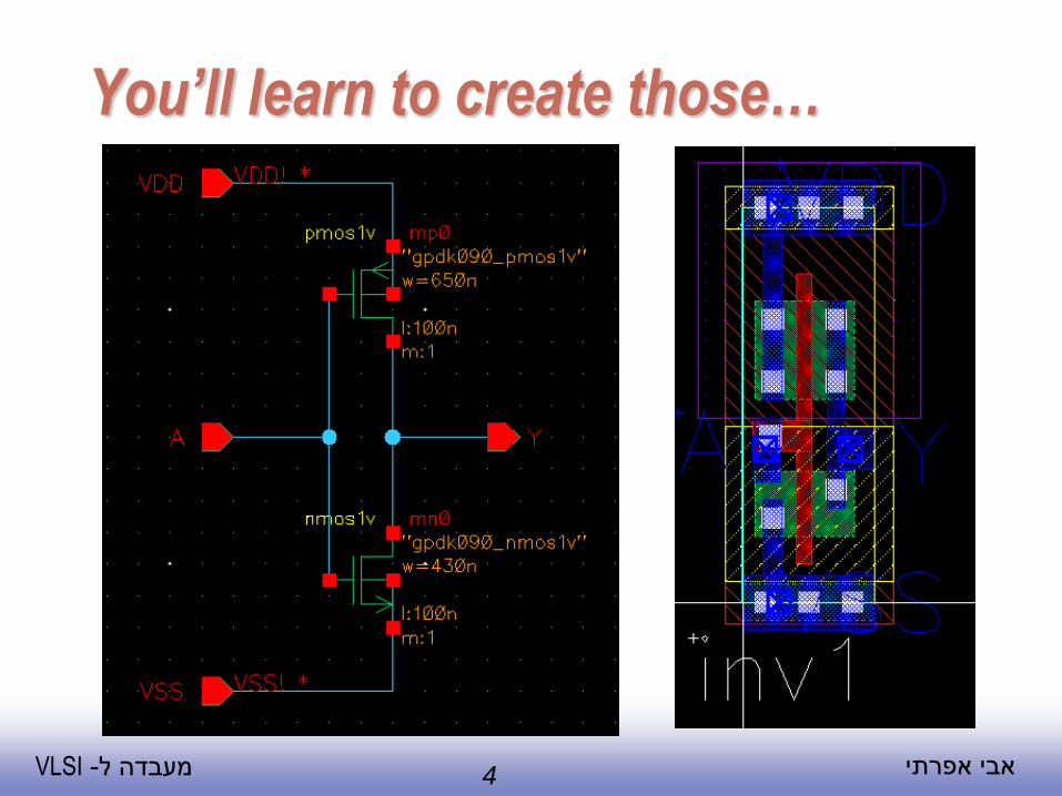
You’ll learn to create those…
5 אבי אפרתי VLSI -מעבדה ל
First access and Login
6 אבי אפרתי VLSI -מעבדה ל
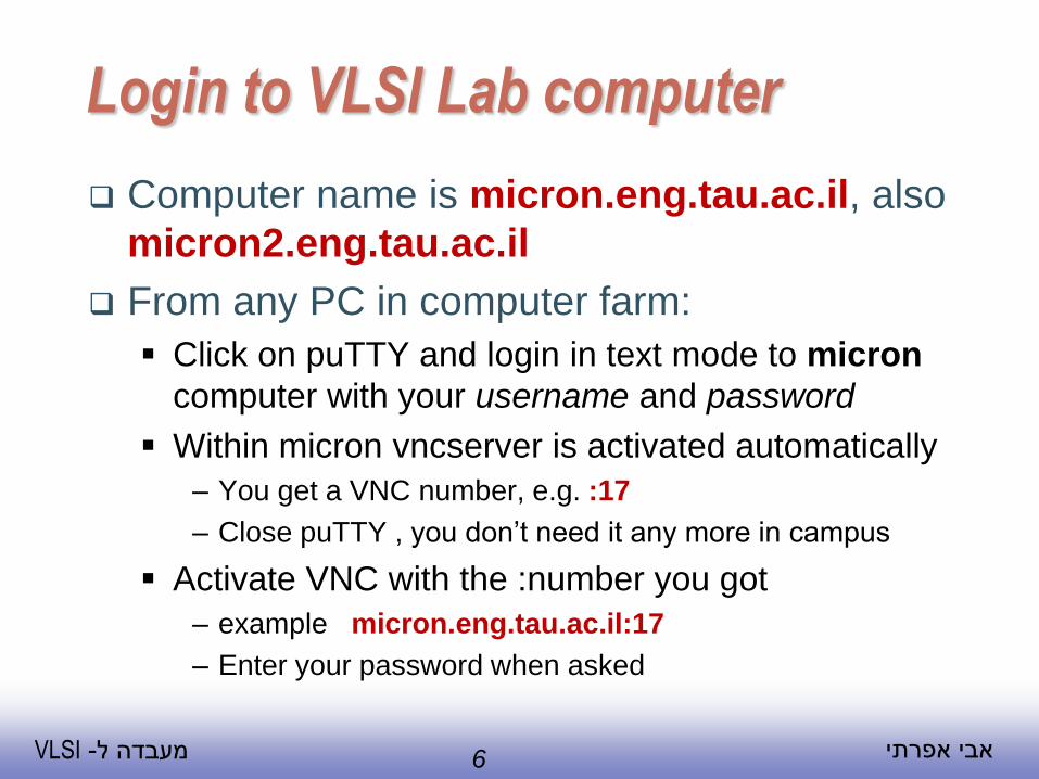
Login to VLSI Lab computer
Computer name is micron.eng.tau.ac.il, also
micron2.eng.tau.ac.il
From any PC in computer farm:
Click on puTTY and login in text mode to micron
computer with your username and password
Within micron vncserver is activated automatically
– You get a VNC number, e.g. :17
– Close puTTY , you don’t need it any more in campus
Activate VNC with the :number you got
– example micron.eng.tau.ac.il:17
– Enter your password when asked
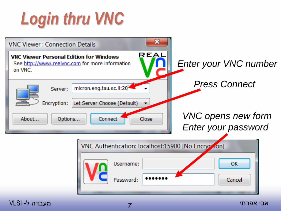
7 אבי אפרתי VLSI -מעבדה ל
Login thru VNC
Enter your VNC number
VNC opens new form
Enter your password
Press Connect
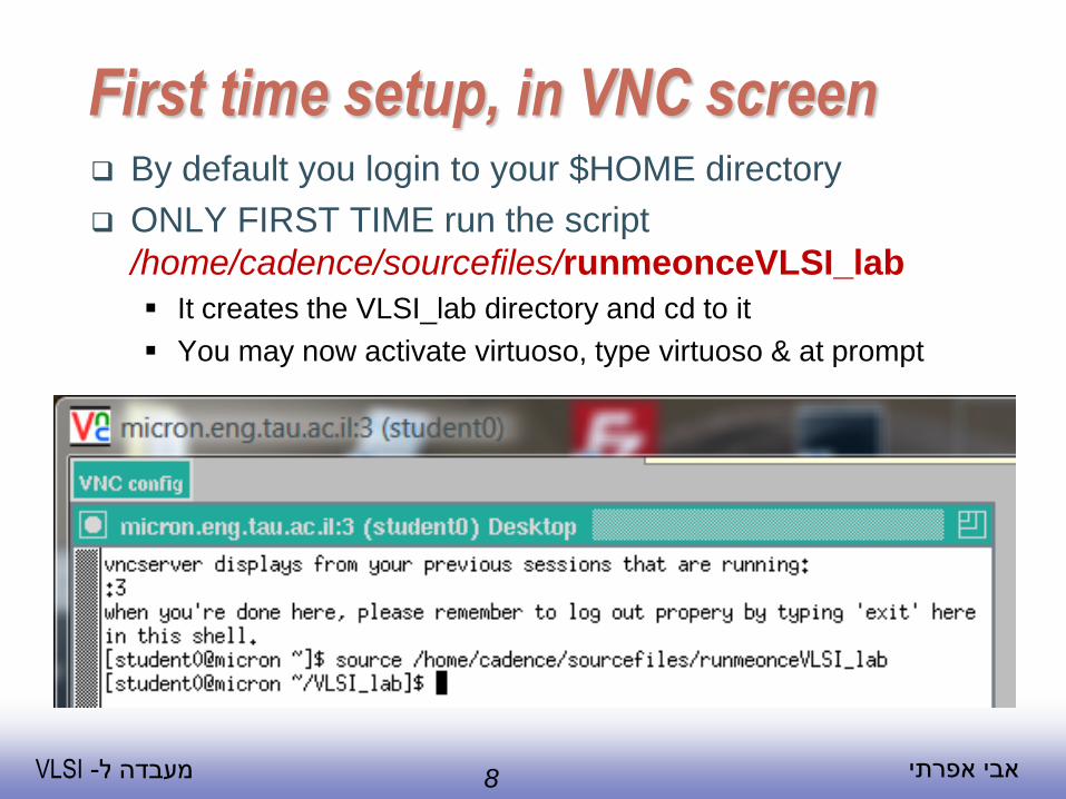
8 אבי אפרתי VLSI -מעבדה ל
First time setup, in VNC screen By default you login to your $HOME directory
ONLY FIRST TIME run the script
/home/cadence/sourcefiles/runmeonceVLSI_lab
It creates the VLSI_lab directory and cd to it
You may now activate virtuoso, type virtuoso & at prompt
9 אבי אפרתי VLSI -מעבדה ל
Regular login campus
Start VNC to micron or micron2
use your VNC number, e.g. micron.eng.tau.ac.il:4
Within VNC screen:
The first xterm appears, click in it and work in text
mode
cd VLSI_lab change directory to VLSI_lab
virtuoso & activate virtuoso
AT ANY TIME you may create additional xterm’s
by mouse left-click and chose xterm from menu
10 אבי אפרתי VLSI -מעבדה ל
Regular login from home Login to gate.tau.ac.il thru puTTY
When working from home DON’T close puTTY
Start VNC to localhost
use your VNC number preceeded by 59, e.g.
localhost:5904
Within VNC screen:
The first xterm appears, click in it and work in text
mode
cd VLSI_lab change directory to VLSI_lab
virtuoso & activate virtuoso
AT ANY TIME you may create additional xterm’s by
mouse left-click and chose xterm from menu
Working from home is not guaranteed
11 אבי אפרתי VLSI -מעבדה ל
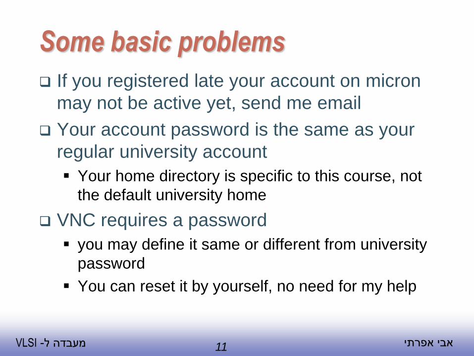
Some basic problems
If you registered late your account on micron
may not be active yet, send me email
Your account password is the same as your
regular university account
Your home directory is specific to this course, not
the default university home
VNC requires a password
you may define it same or different from university
password
You can reset it by yourself, no need for my help
12 אבי אפרתי VLSI -מעבדה ל
Creating a Design
13 אבי אפרתי VLSI -מעבדה ל
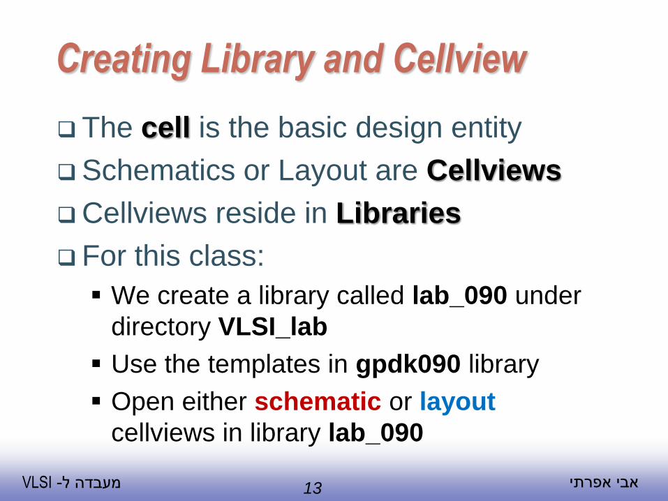
Creating Library and Cellview
The cell is the basic design entity
Schematics or Layout are Cellviews
Cellviews reside in Libraries
For this class:
We create a library called lab_090 under
directory VLSI_lab
Use the templates in gpdk090 library
Open either schematic or layout
cellviews in library lab_090
14 אבי אפרתי VLSI -מעבדה ל
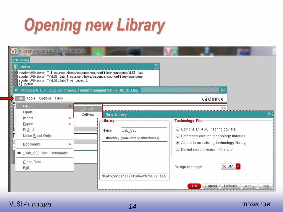
Opening new Library
15 אבי אפרתי VLSI -מעבדה ל
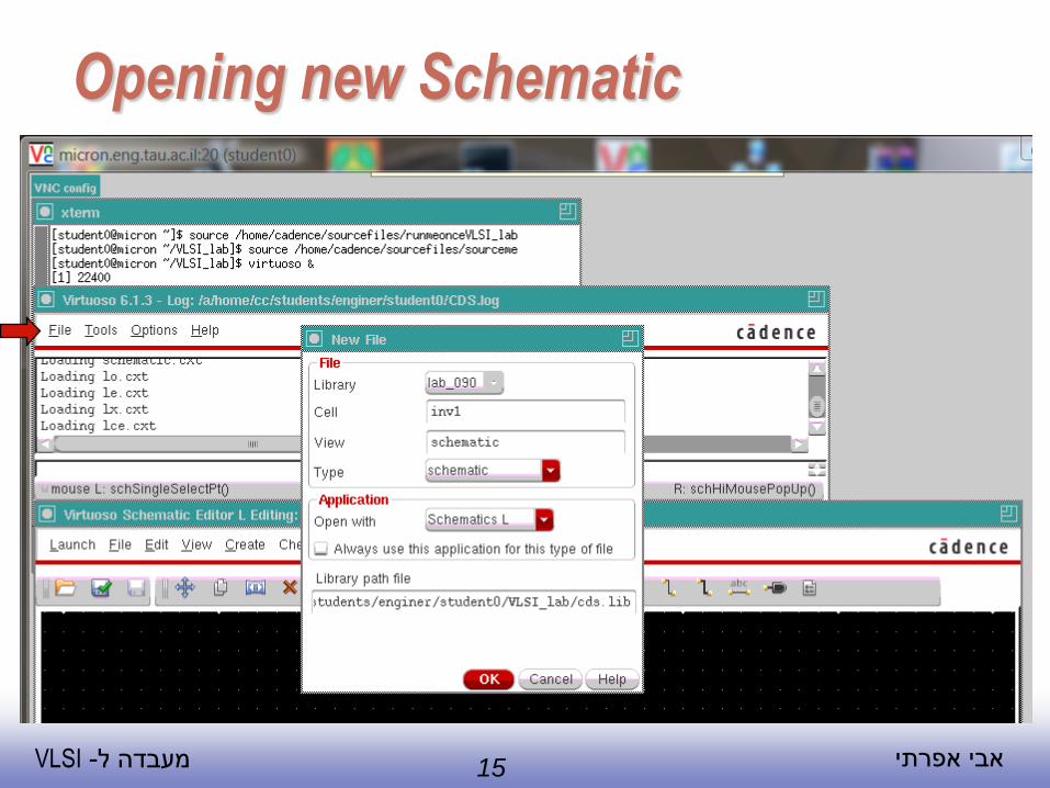
Opening new Schematic
16 אבי אפרתי VLSI -מעבדה ל
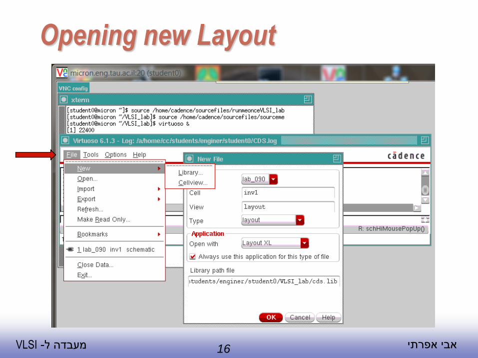
Opening new Layout
17 אבי אפרתי VLSI -מעבדה ל
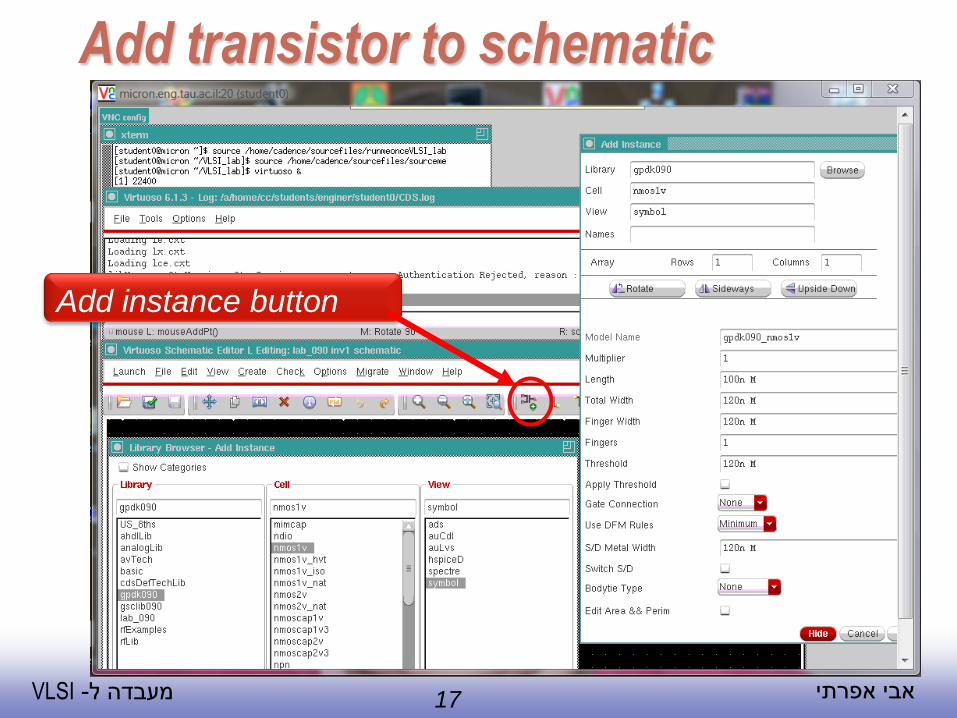
Add transistor to schematic
Add instance button
18 אבי אפרתי VLSI -מעבדה ל
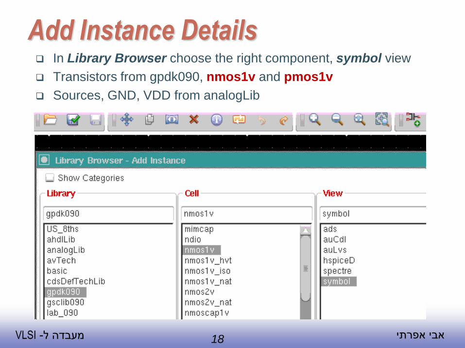
Add Instance Details In Library Browser choose the right component, symbol view
Transistors from gpdk090, nmos1v and pmos1v
Sources, GND, VDD from analogLib
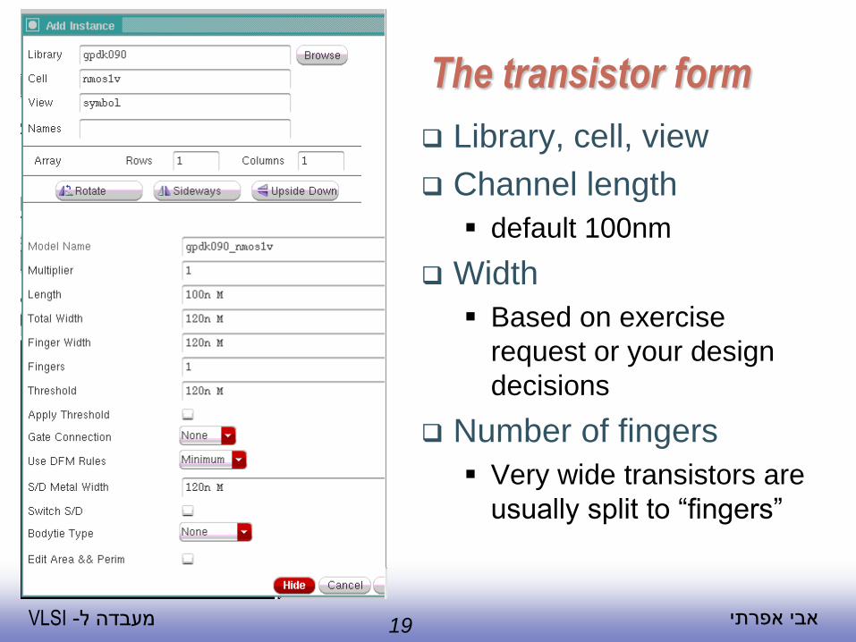
19 אבי אפרתי VLSI -מעבדה ל
The transistor form
Library, cell, view
Channel length
default 100nm
Width
Based on exercise
request or your design
decisions
Number of fingers
Very wide transistors are
usually split to “fingers”
20 אבי אפרתי VLSI -מעבדה ל
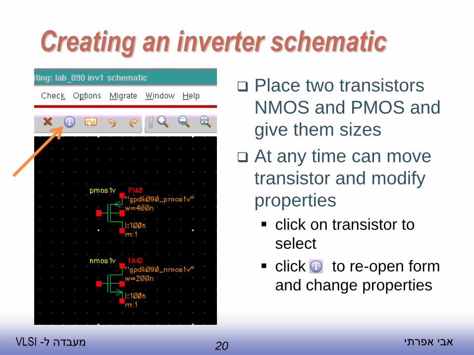
Creating an inverter schematic
Place two transistors
NMOS and PMOS and
give them sizes
At any time can move
transistor and modify
properties
click on transistor to
select
click to re-open form
and change properties
21 אבי אפרתי VLSI -מעבדה ל
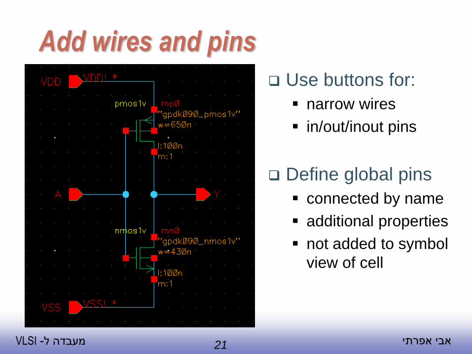
Add wires and pins
Use buttons for:
narrow wires
in/out/inout pins
Define global pins
connected by name
additional properties
not added to symbol
view of cell
22 אבי אפרתי VLSI -מעבדה ל
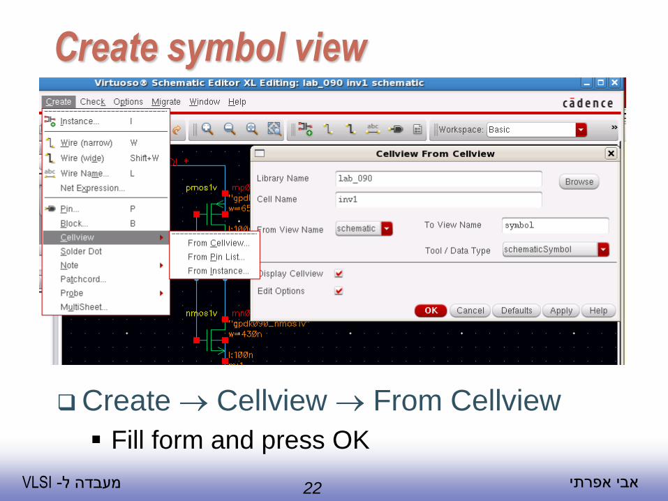
Create symbol view
Create Cellview From Cellview
Fill form and press OK
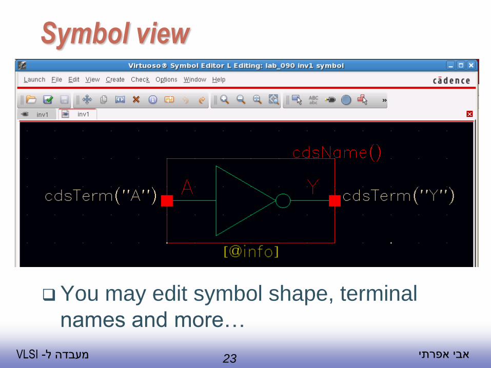
23 אבי אפרתי VLSI -מעבדה ל
Symbol view
You may edit symbol shape, terminal
names and more…
24 אבי אפרתי VLSI -מעבדה ל
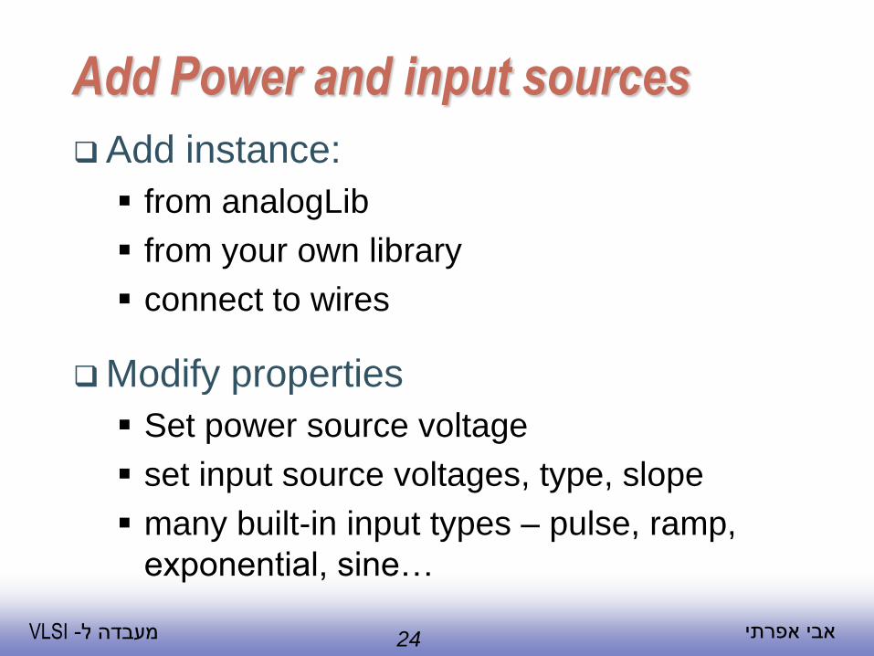
Add Power and input sources
Add instance:
from analogLib
from your own library
connect to wires
Modify properties
Set power source voltage
set input source voltages, type, slope
many built-in input types – pulse, ramp,
exponential, sine…
25 אבי אפרתי VLSI -מעבדה ל
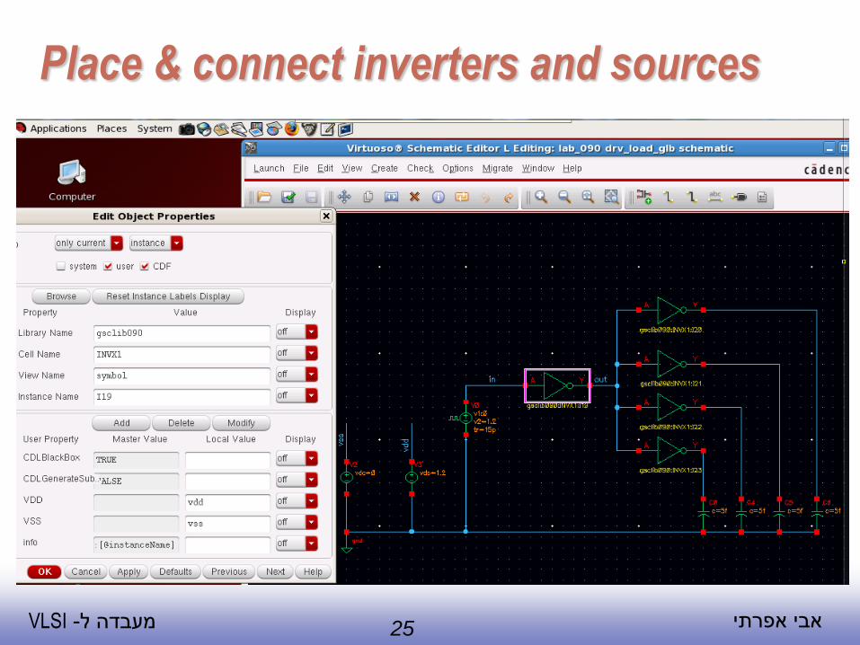
Place & connect inverters and sources
26 אבי אפרתי VLSI -מעבדה ל
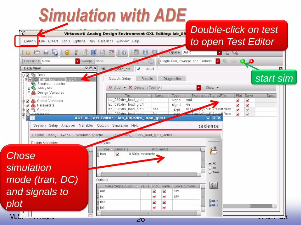
Simulation with ADE
Chose
simulation
mode (tran, DC)
and signals to
plot
Double-click on test
to open Test Editor
start sim
27 אבי אפרתי VLSI -מעבדה ל
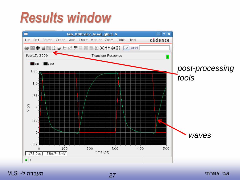
Results window
waves
post-processing
tools
28 אבי אפרתי VLSI -מעבדה ל
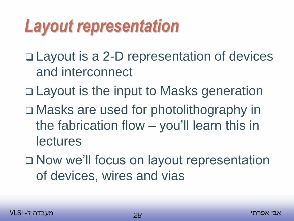
Layout representation
Layout is a 2-D representation of devices
and interconnect
Layout is the input to Masks generation
Masks are used for photolithography in
the fabrication flow – you’ll learn this in
lectures
Now we’ll focus on layout representation
of devices, wires and vias
29 אבי אפרתי VLSI -מעבדה ל
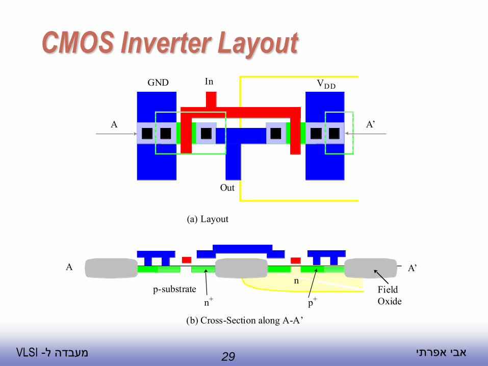
CMOS Inverter Layout
A A’
np-substrate Field
Oxidep+n+
In
Out
GND VDD
(a) Layout
(b) Cross-Section along A-A’
A A’
30 אבי אפרתי VLSI -מעבדה ל
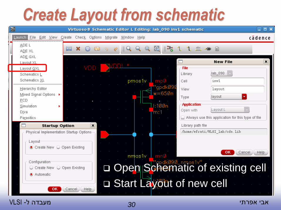
Create Layout from schematic
Open Schematic of existing cell
Start Layout of new cell
31 אבי אפרתי VLSI -מעבדה ל
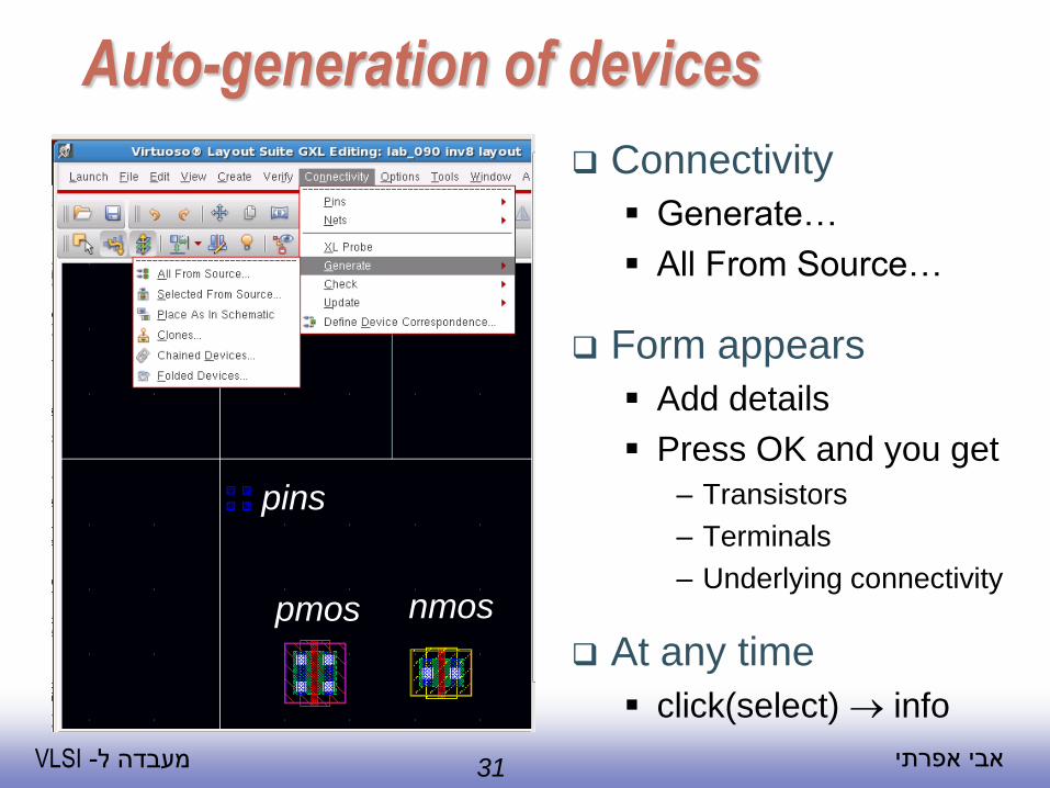
Auto-generation of devices
Connectivity
Generate…
All From Source…
Form appears
Add details
Press OK and you get
– Transistors
– Terminals
– Underlying connectivity
At any time
click(select) info
nmos pmos
pins
32 אבי אפרתי VLSI -מעבדה ל
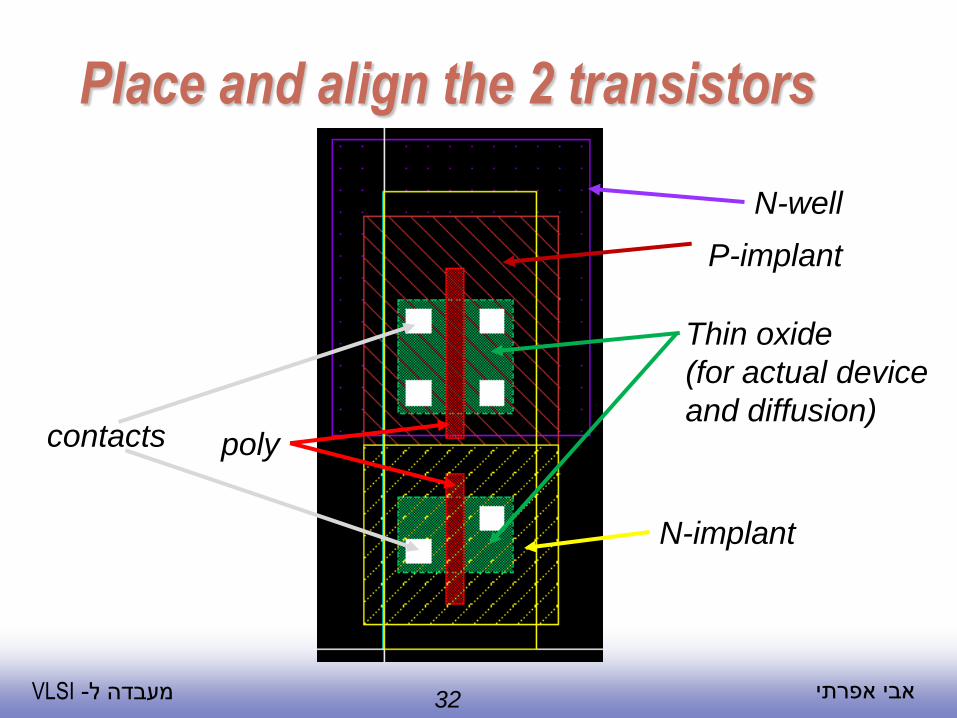
Place and align the 2 transistors
N-well
Thin oxide
(for actual device
and diffusion)
P-implant
N-implant
poly contacts
33 אבי אפרתי VLSI -מעבדה ל
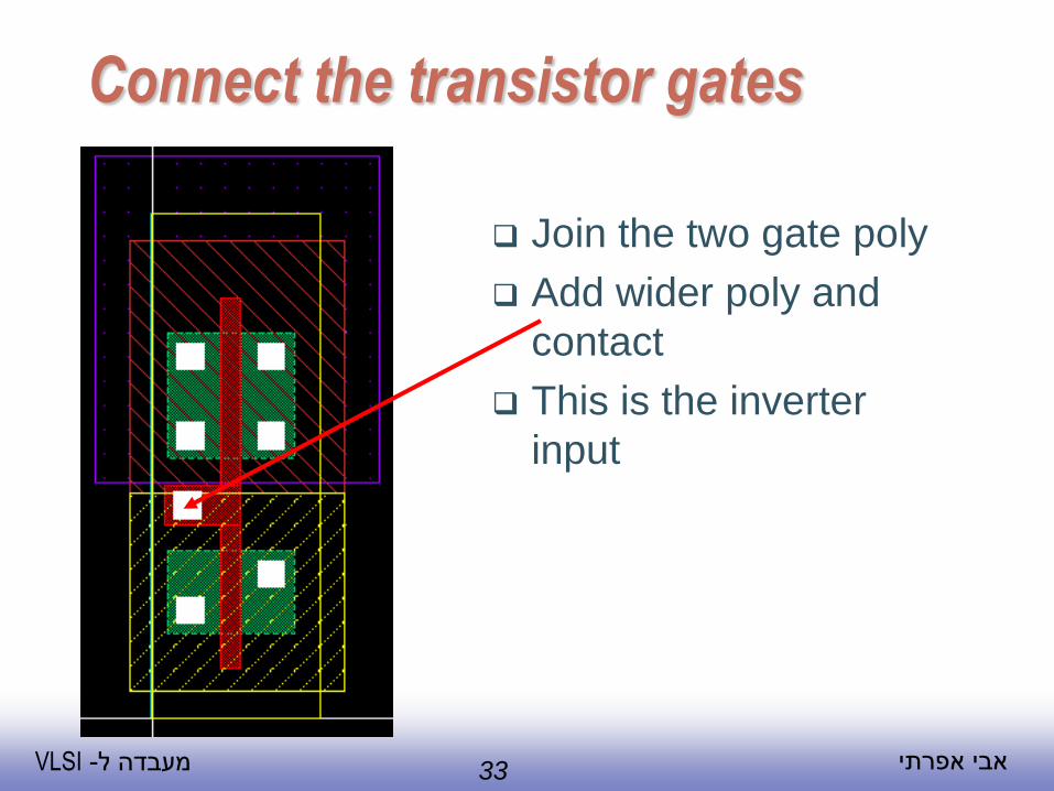
Connect the transistor gates
Join the two gate poly
Add wider poly and
contact
This is the inverter
input
34 אבי אפרתי VLSI -מעבדה ל
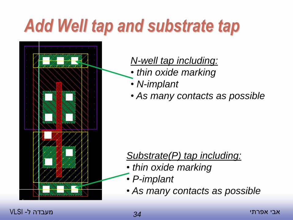
Add Well tap and substrate tap
N-well tap including:
• thin oxide marking
• N-implant
• As many contacts as possible
Substrate(P) tap including:
• thin oxide marking
• P-implant
• As many contacts as possible
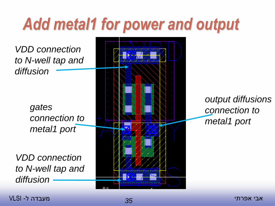
35 אבי אפרתי VLSI -מעבדה ל
Add metal1 for power and output
gates
connection to
metal1 port
VDD connection
to N-well tap and
diffusion
VDD connection
to N-well tap and
diffusion
output diffusions
connection to
metal1 port
36 אבי אפרתי VLSI -מעבדה ל
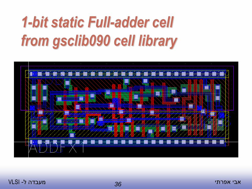
1-bit static Full-adder cell
from gsclib090 cell library
37 אבי אפרתי VLSI -מעבדה ל
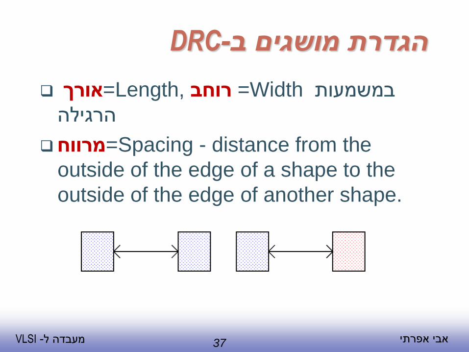
DRC-הגדרת מושגים ב
רוחב ,Length=אורך =Width במשמעות
הרגילה
מרווח=Spacing - distance from the
outside of the edge of a shape to the
outside of the edge of another shape.
38 אבי אפרתי VLSI -מעבדה ל
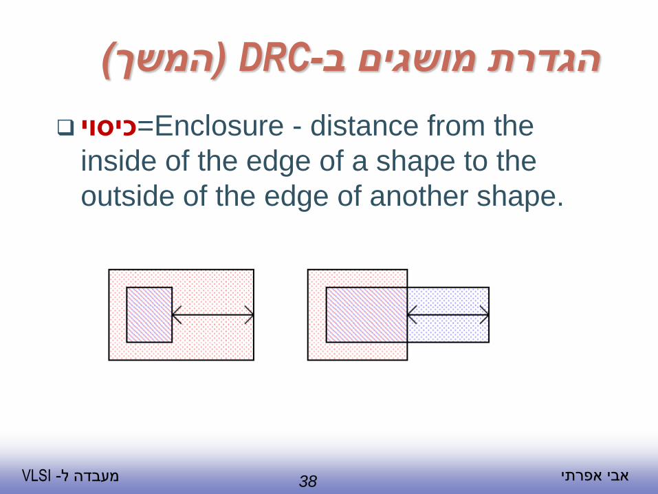
(המשך) DRC-הגדרת מושגים ב
Enclosure - distance from the=כיסוי
inside of the edge of a shape to the
outside of the edge of another shape.
39 אבי אפרתי VLSI -מעבדה ל
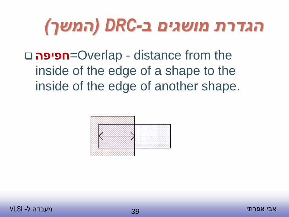
(המשך) DRC-הגדרת מושגים ב
חפיפה=Overlap - distance from the
inside of the edge of a shape to the
inside of the edge of another shape.
40 אבי אפרתי VLSI -מעבדה ל
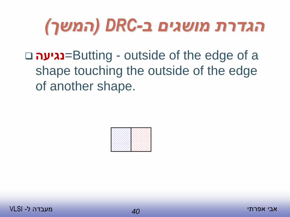
(המשך) DRC-הגדרת מושגים ב
נגיעה=Butting - outside of the edge of a
shape touching the outside of the edge
of another shape.
41 אבי אפרתי VLSI -מעבדה ל
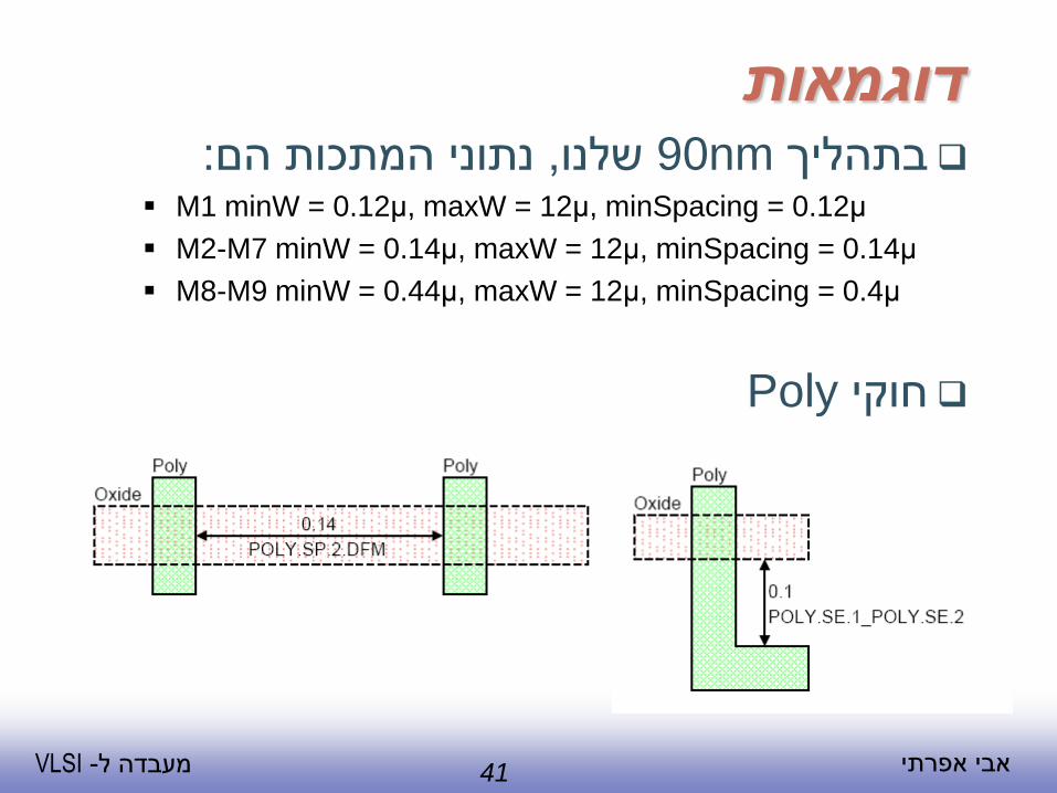
דוגמאות 90בתהליךnm נתוני המתכות הם, שלנו:
M1 minW = 0.12μ, maxW = 12μ, minSpacing = 0.12μ
M2-M7 minW = 0.14μ, maxW = 12μ, minSpacing = 0.14μ
M8-M9 minW = 0.44μ, maxW = 12μ, minSpacing = 0.4μ
חוקיPoly


![Schematics Behringer Pmx2000 [ET]](https://img.pdfslide.tips/doc/110x75/54153d127bef0a7f3f8b4743/schematics-behringer-pmx2000-et.jpg)