Embed Size (px)
Citation preview
BiTS China 2016
September 13, 2016 Burn-in & Test Strategies Workshop www.bitsworkshop.org
Premium Archive
Session 2 September 13, 2016
© 2016 BiTS Workshop – Image: 一花一菩提/HuiTu.com
BiTS China 2016
September 13, 2016 Burn-in & Test Strategies Workshop www.bitsworkshop.org
Premium Archive
Presentation / Copyright Notice The presentations in this publication comprise the pre-workshop Proceedings of the BiTS China Workshop. They reflect the authors’ opinions and are reproduced here as they are planned to be presented at the BiTS China Workshop. Updates from this version of the papers may occur in the version that is actually presented at the BiTS China Workshop. The inclusion of the papers in this publication does not constitute an endorsement by the BiTS Workshop or the sponsors. There is NO copyright protection claimed by this publication. However, each presentation is the work of the authors and their respective companies: as such, it is strongly encouraged that any use reflect proper acknowledgement to the appropriate source. Any questions regarding the use of any materials presented should be directed to the author/s or their companies. The BiTS logo, ‘Burn-in & Test Strategies Workshop’, ‘BiTS China’, and ‘Burn-in & Test Strategies China Workshop’ are trademarks of BiTS Workshop.
1
BiTS China 2016
September 13, 2016 Burn-in & Test Strategies Workshop www.bitsworkshop.org
Premium Archive
Session
Session Chair
BiTS China
Socket Technology
"Study of Probe Pin Internal Resistance" Takuto Yoshida - Test Tooling Solutions Group
"Monte Carlo Analysis for PoP Alignment" DeXian (Frank) Liu - Smiths Connectors
"Conductive Elastomer vs Spring Probe: Performance & Application"
Jiachun (Frank) Zhou - Smiths Connectors
"Do Socket and Kits Design Matter for Die Cracking?"
Yuanjun Shi - TwinSolution Technology
2 Frank Zhou
BiTS China 2016
September 13, 2016 Burn-in & Test Strategies Workshop www.bitsworkshop.org
Premium Archive
Session
Session Chair
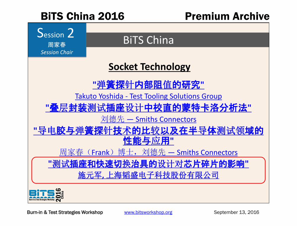
BiTS China
Socket Technology
"弹簧探针内部阻值的研究" Takuto Yoshida - Test Tooling Solutions Group
"叠层封装测试插座设计中校直的蒙特卡洛分析法" 刘德先 — Smiths Connectors
"导电胶与弹簧探针技术的比较以及在半导体测试领域的性能与应用"
周家春(Frank)博士,刘德先 — Smiths Connectors
"测试插座和快速切换治具的设计对芯片碎片的影响" 施元军, 上海韬盛电子科技股份有限公司
2 周家春
Socket TechnologyBiTS China 2016Session 2 Presentation 4
September 13, 2016Burn-in & Test Strategies Workshop www.bitsworkshop.org
Do Socket and Kit Designs
Matter for Die Cracking?
Yuanjun Shi, Kane Liu
Twinsolution Technology (Suzhou) Ltd.
BiTS China Workshop
Suzhou
September 13, 2016
Conference Ready
mm/dd/2014
Socket TechnologyBiTS China 2016Session 2 Presentation 4
September 13, 2016Burn-in & Test Strategies Workshop www.bitsworkshop.org
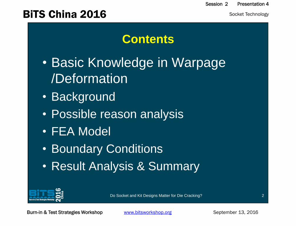
Contents
• Basic Knowledge in Warpage
/Deformation
• Background
• Possible reason analysis
• FEA Model
• Boundary Conditions
• Result Analysis & Summary
2Do Socket and Kit Designs Matter for Die Cracking?
Socket TechnologyBiTS China 2016Session 2 Presentation 4
September 13, 2016Burn-in & Test Strategies Workshop www.bitsworkshop.org
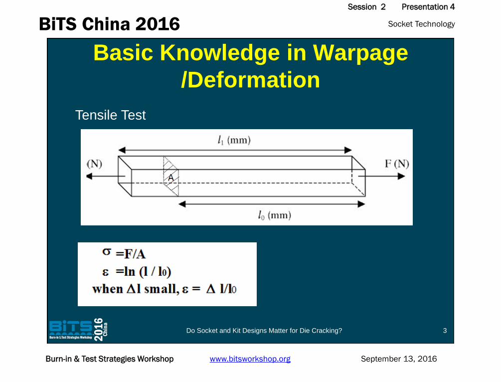
Basic Knowledge in Warpage
/Deformation
Tensile Test
3Do Socket and Kit Designs Matter for Die Cracking?
Socket TechnologyBiTS China 2016Session 2 Presentation 4
September 13, 2016Burn-in & Test Strategies Workshop www.bitsworkshop.org
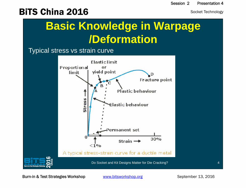
Typical stress vs strain curve
Basic Knowledge in Warpage
/Deformation
4Do Socket and Kit Designs Matter for Die Cracking?
Socket TechnologyBiTS China 2016Session 2 Presentation 4
September 13, 2016Burn-in & Test Strategies Workshop www.bitsworkshop.org
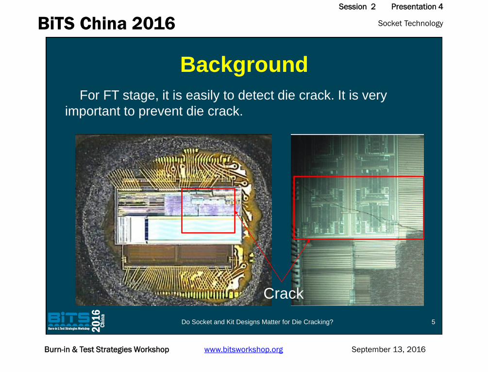
For FT stage, it is easily to detect die crack. It is very
important to prevent die crack.
Crack
Background
5Do Socket and Kit Designs Matter for Die Cracking?
Socket TechnologyBiTS China 2016Session 2 Presentation 4
September 13, 2016Burn-in & Test Strategies Workshop www.bitsworkshop.org
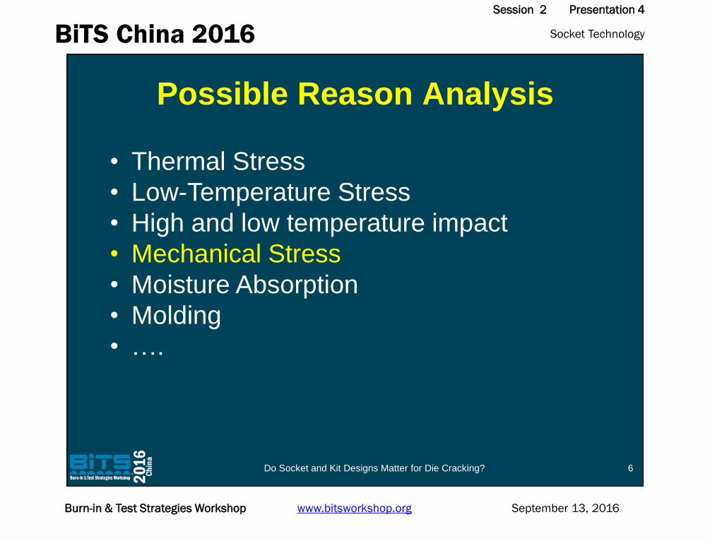
• Thermal Stress
• Low-Temperature Stress
• High and low temperature impact
• Mechanical Stress
• Moisture Absorption
• Molding
• ….
Possible Reason Analysis
6Do Socket and Kit Designs Matter for Die Cracking?
Socket TechnologyBiTS China 2016Session 2 Presentation 4
September 13, 2016Burn-in & Test Strategies Workshop www.bitsworkshop.org
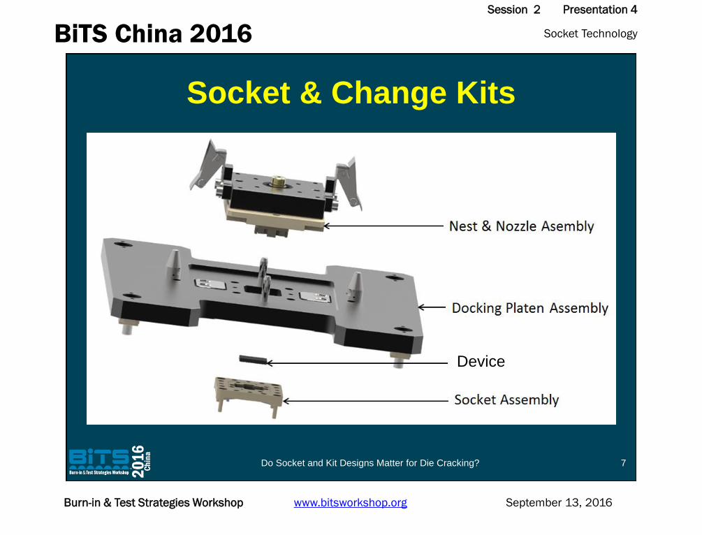
Socket & Change Kits
Device
7Do Socket and Kit Designs Matter for Die Cracking?
Socket TechnologyBiTS China 2016Session 2 Presentation 4
September 13, 2016Burn-in & Test Strategies Workshop www.bitsworkshop.org
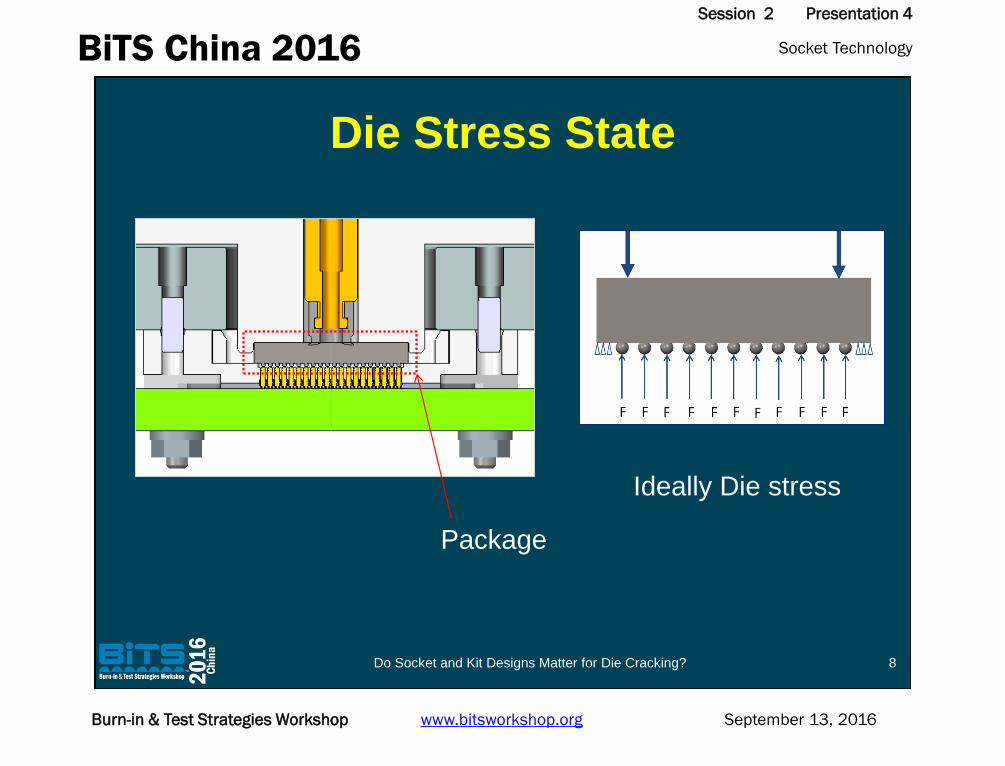
Package
Ideally Die stress
Die Stress State
8Do Socket and Kit Designs Matter for Die Cracking?
Socket TechnologyBiTS China 2016Session 2 Presentation 4
September 13, 2016Burn-in & Test Strategies Workshop www.bitsworkshop.org
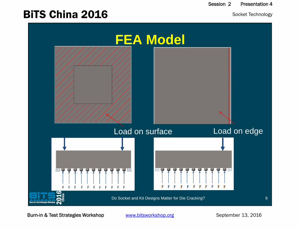
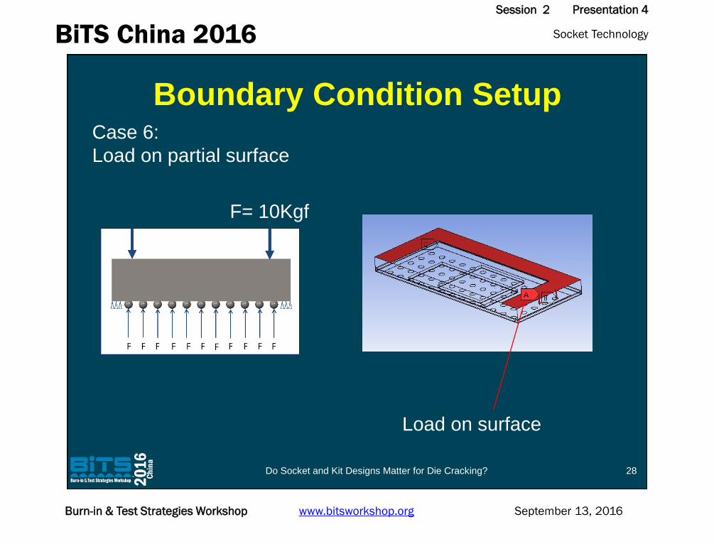
Load on surface Load on edge
FEA Model
9Do Socket and Kit Designs Matter for Die Cracking?
Socket TechnologyBiTS China 2016Session 2 Presentation 4
September 13, 2016Burn-in & Test Strategies Workshop www.bitsworkshop.org
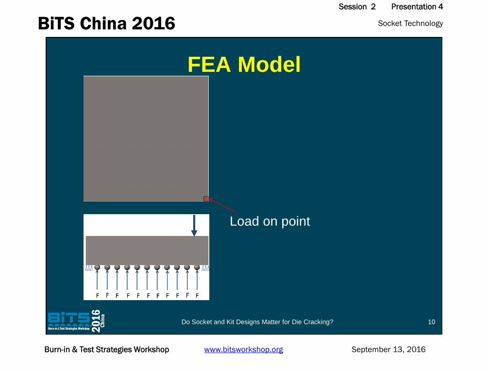
Load on point
FEA Model
10Do Socket and Kit Designs Matter for Die Cracking?
Socket TechnologyBiTS China 2016Session 2 Presentation 4
September 13, 2016Burn-in & Test Strategies Workshop www.bitsworkshop.org
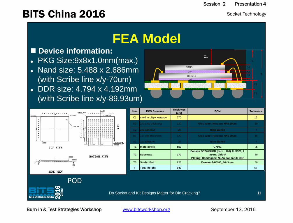
DAF
DDRx16
DAF
NAND
C1
A1
D1
A2
D2
T1
T2
T3
T
Item PKG StructureThickness
(um)BOM Tolerance
C1 mold to chip clearance 270 15
D2 2nd chip thickness 120 Gold wire: Heraeus HA6 20um 10
A2 2nd adhesive 20 Nitto EM760 4
D1 1st chip thickness 120 Gold wire: Heraeus HA6 20um 10
A1 1st adhesive 20 Nitto EM760 4
T1 mold cavity 550 G760L 25
T2 Substrate 170
Doosan DS7409HGB (core : 100) AUS320, 2
layers, 2block
Plating: Bondfigner: Ni/Au ball land: OSP
30
T3 Solder Ball 220 Duksan SAC105_Φ0.3mm 50
T Total height 940 63
Device information:
PKG Size:9x8x1.0mm(max.)
Nand size: 5.488 x 2.686mm
(with Scribe line x/y-70um)
DDR size: 4.794 x 4.192mm
(with Scribe line x/y-89.93um)
FEA Model
POD
11Do Socket and Kit Designs Matter for Die Cracking?
Socket TechnologyBiTS China 2016Session 2 Presentation 4
September 13, 2016Burn-in & Test Strategies Workshop www.bitsworkshop.org
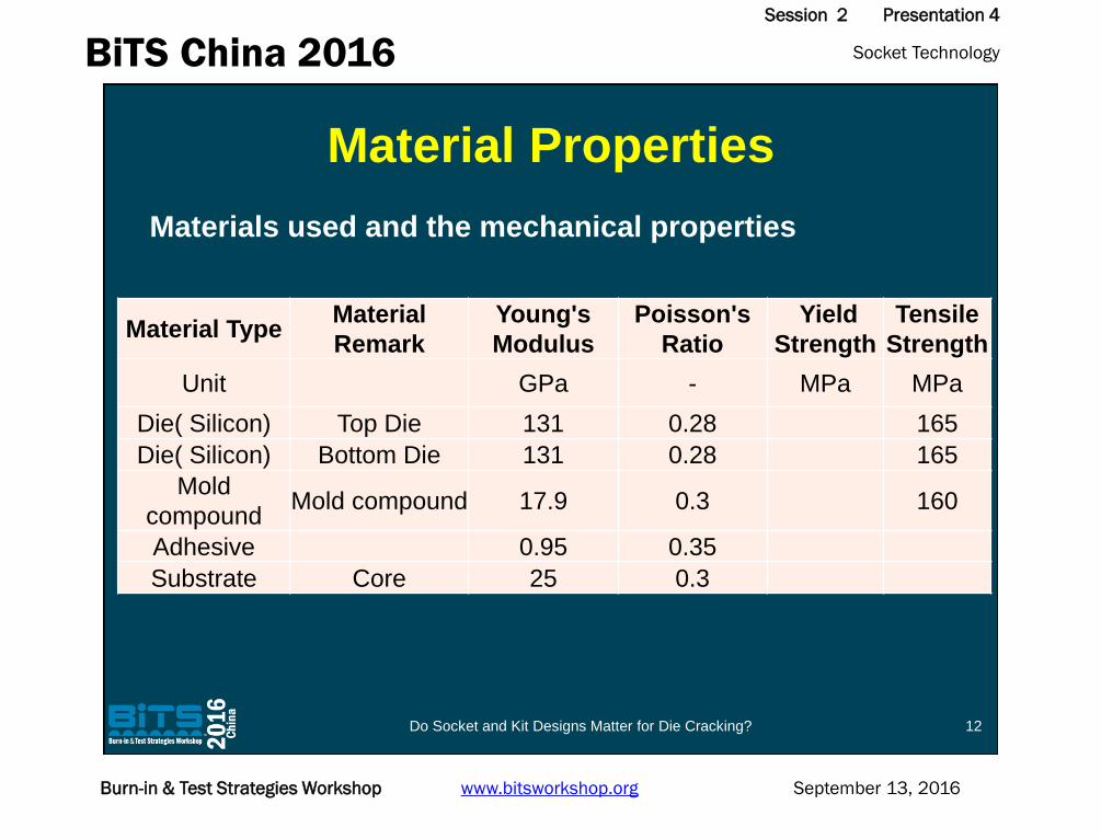
Materials used and the mechanical properties
Material TypeMaterial
Remark
Young's
Modulus
Poisson's
Ratio
Yield
Strength
Tensile
Strength
Unit GPa - MPa MPa
Die( Silicon) Top Die 131 0.28 165
Die( Silicon) Bottom Die 131 0.28 165
Mold
compound Mold compound 17.9 0.3 160
Adhesive 0.95 0.35
Substrate Core 25 0.3
Material Properties
12Do Socket and Kit Designs Matter for Die Cracking?
Socket TechnologyBiTS China 2016Session 2 Presentation 4
September 13, 2016Burn-in & Test Strategies Workshop www.bitsworkshop.org
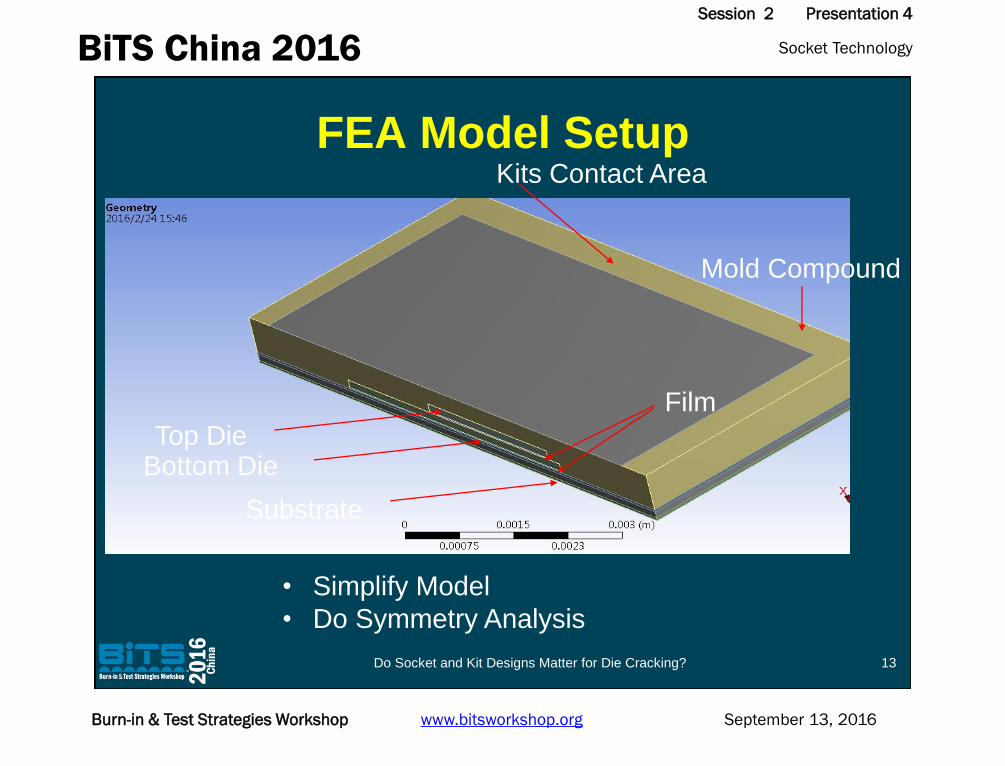
Mold Compound
Kits Contact Area
Top DieBottom Die
Substrate
Film
• Simplify Model
• Do Symmetry Analysis
FEA Model Setup
13Do Socket and Kit Designs Matter for Die Cracking?
Socket TechnologyBiTS China 2016Session 2 Presentation 4
September 13, 2016Burn-in & Test Strategies Workshop www.bitsworkshop.org
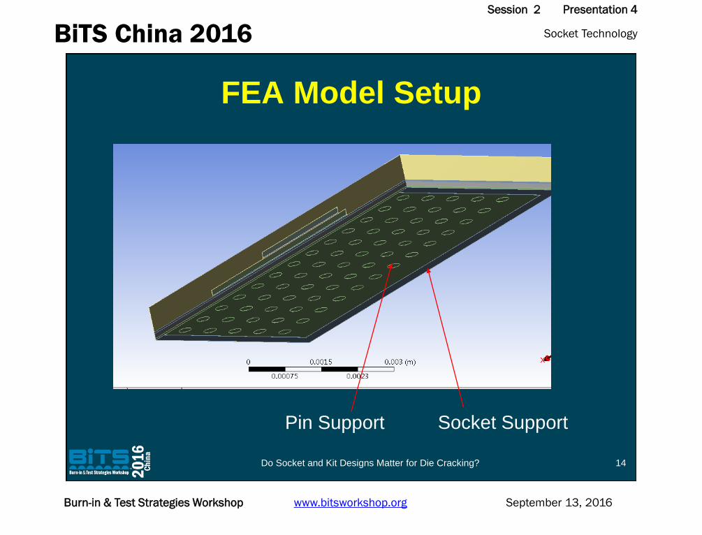
Pin Support Socket Support
FEA Model Setup
14Do Socket and Kit Designs Matter for Die Cracking?
Socket TechnologyBiTS China 2016Session 2 Presentation 4
September 13, 2016Burn-in & Test Strategies Workshop www.bitsworkshop.org
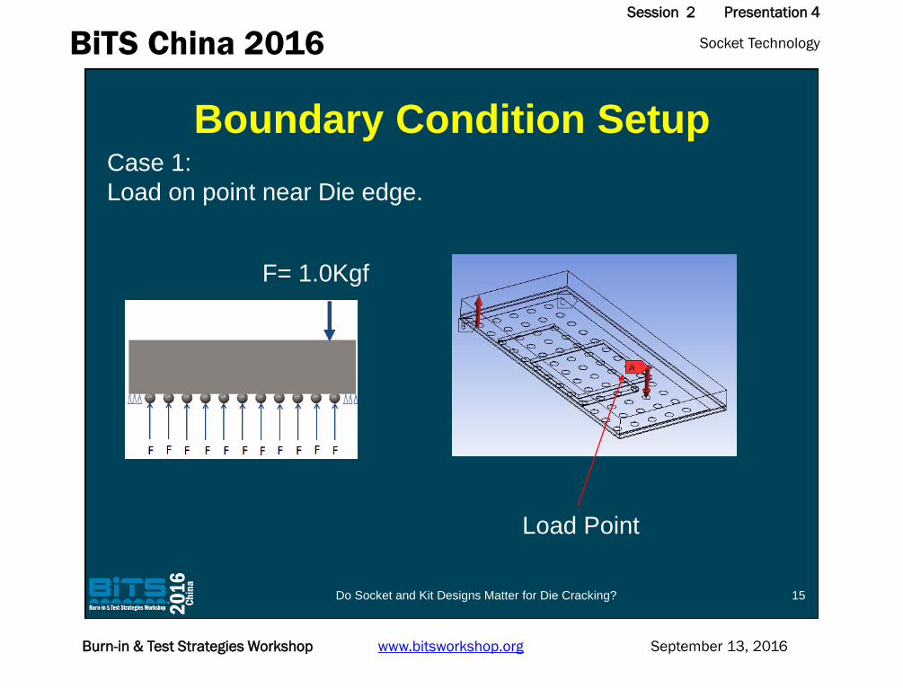
F= 1.0Kgf
Case 1:
Load on point near Die edge.
Load Point
Boundary Condition Setup
15Do Socket and Kit Designs Matter for Die Cracking?

Socket TechnologyBiTS China 2016Session 2 Presentation 4
September 13, 2016Burn-in & Test Strategies Workshop www.bitsworkshop.org
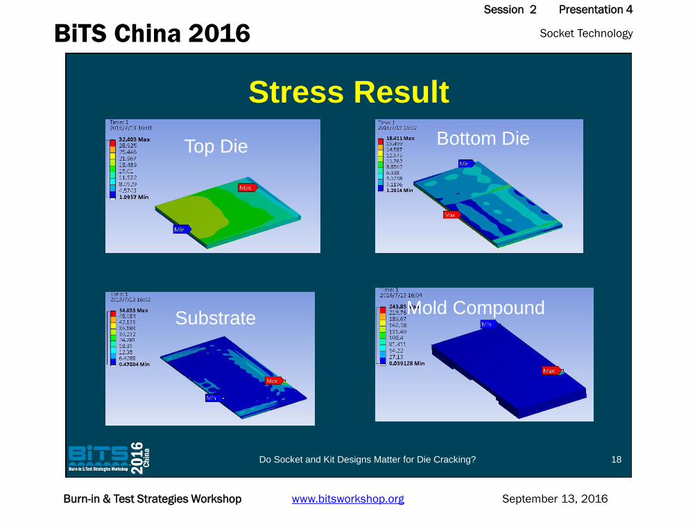
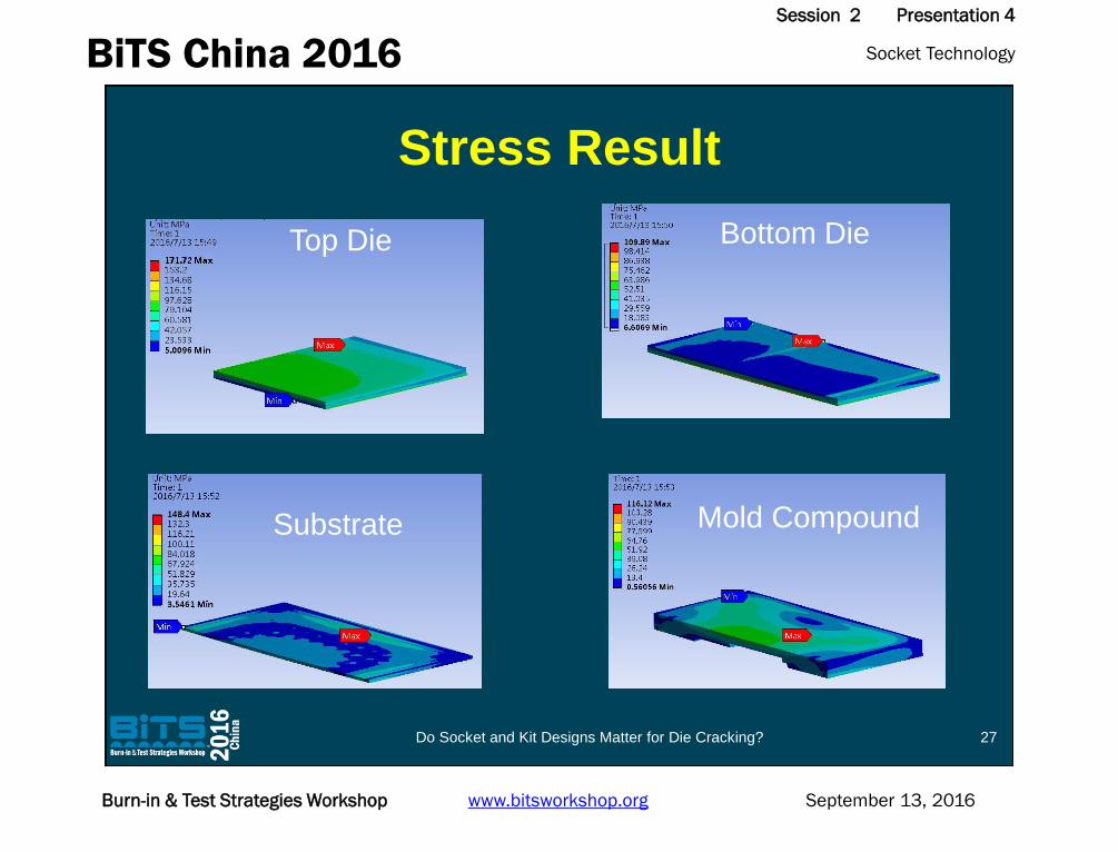
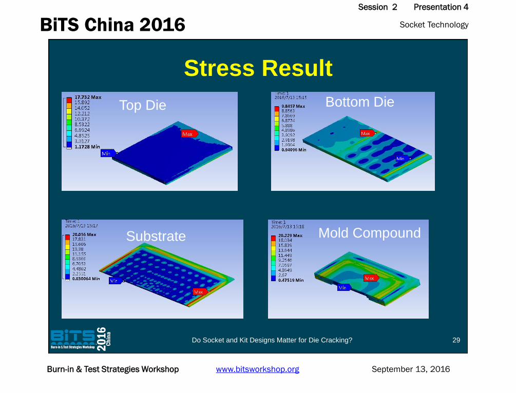
Top Die Bottom Die
Mold CompoundSubstrate
Stress Result
16Do Socket and Kit Designs Matter for Die Cracking?
Socket TechnologyBiTS China 2016Session 2 Presentation 4
September 13, 2016Burn-in & Test Strategies Workshop www.bitsworkshop.org
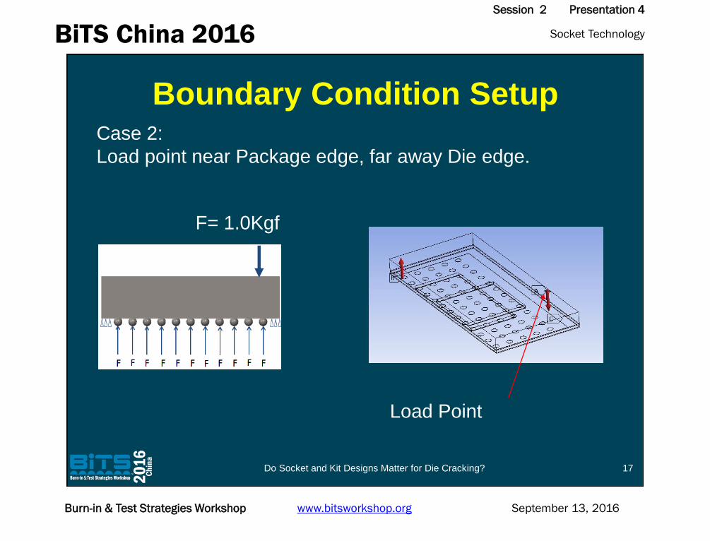
F= 1.0Kgf
Case 2:
Load point near Package edge, far away Die edge.
Load Point
Boundary Condition Setup
17Do Socket and Kit Designs Matter for Die Cracking?
Socket TechnologyBiTS China 2016Session 2 Presentation 4
September 13, 2016Burn-in & Test Strategies Workshop www.bitsworkshop.org
Top Die Bottom Die
Mold CompoundSubstrate
Stress Result
18Do Socket and Kit Designs Matter for Die Cracking?
Socket TechnologyBiTS China 2016Session 2 Presentation 4
September 13, 2016Burn-in & Test Strategies Workshop www.bitsworkshop.org
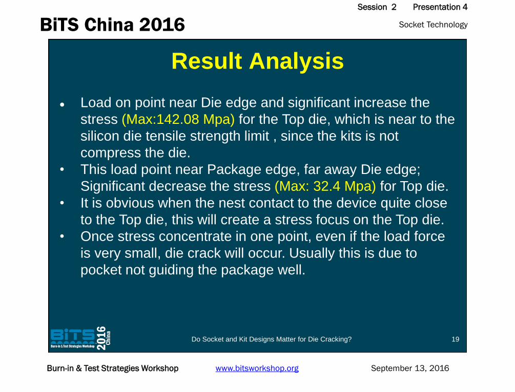
Load on point near Die edge and significant increase the
stress (Max:142.08 Mpa) for the Top die, which is near to the
silicon die tensile strength limit , since the kits is not
compress the die.
• This load point near Package edge, far away Die edge;
Significant decrease the stress (Max: 32.4 Mpa) for Top die.
• It is obvious when the nest contact to the device quite close
to the Top die, this will create a stress focus on the Top die.
• Once stress concentrate in one point, even if the load force
is very small, die crack will occur. Usually this is due to
pocket not guiding the package well.
Result Analysis
19Do Socket and Kit Designs Matter for Die Cracking?
Socket TechnologyBiTS China 2016Session 2 Presentation 4
September 13, 2016Burn-in & Test Strategies Workshop www.bitsworkshop.org
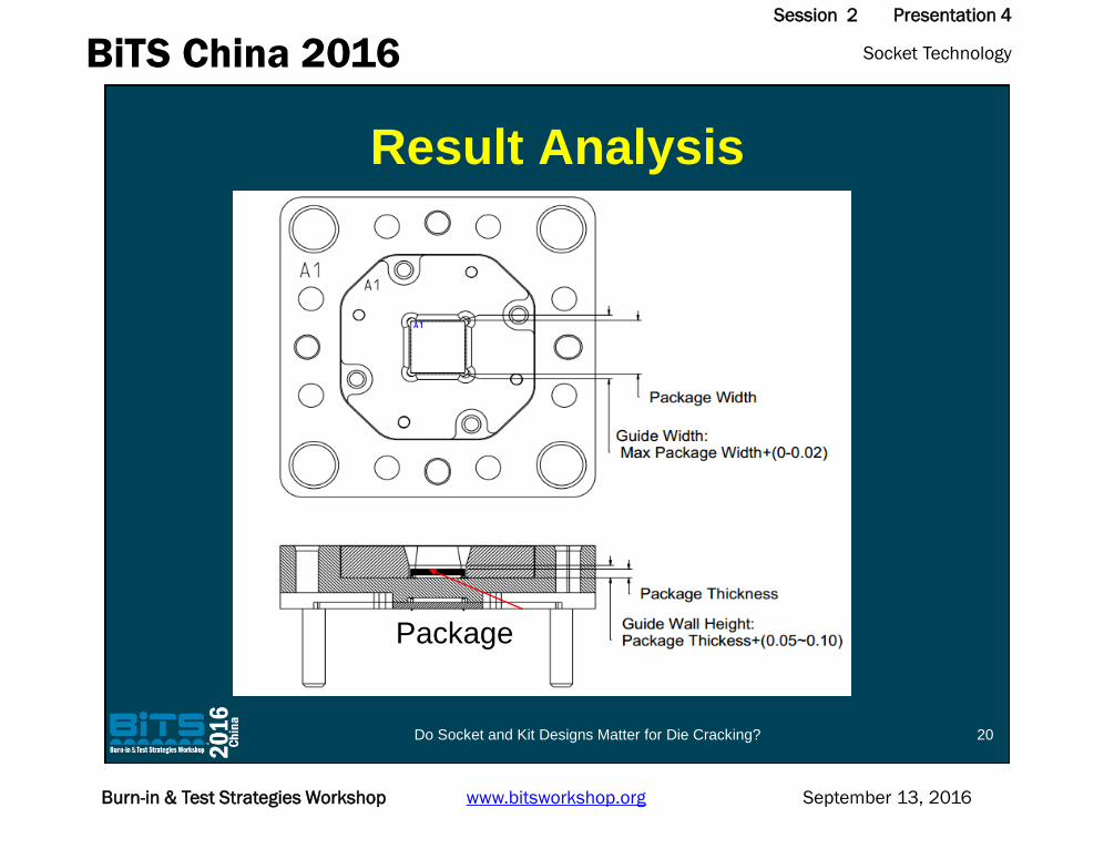
Package
Result Analysis
20Do Socket and Kit Designs Matter for Die Cracking?
Socket TechnologyBiTS China 2016Session 2 Presentation 4
September 13, 2016Burn-in & Test Strategies Workshop www.bitsworkshop.org
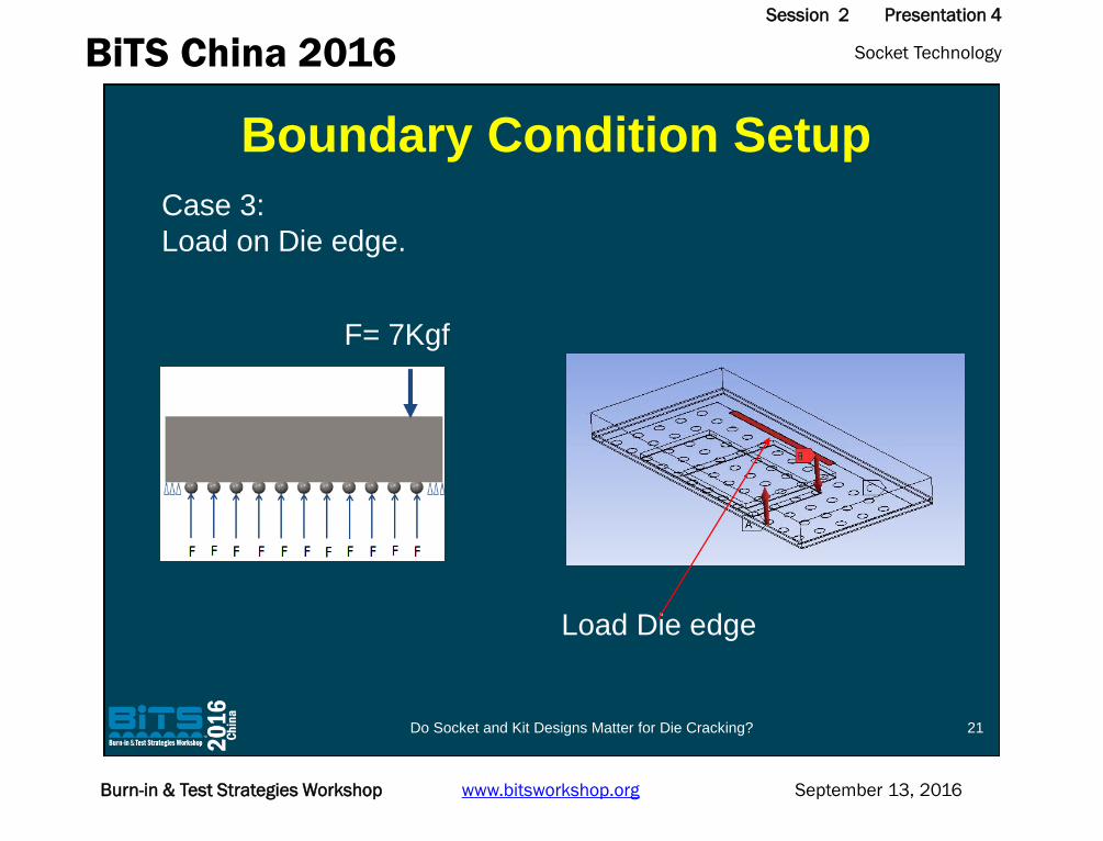
F= 7Kgf
Load Die edge
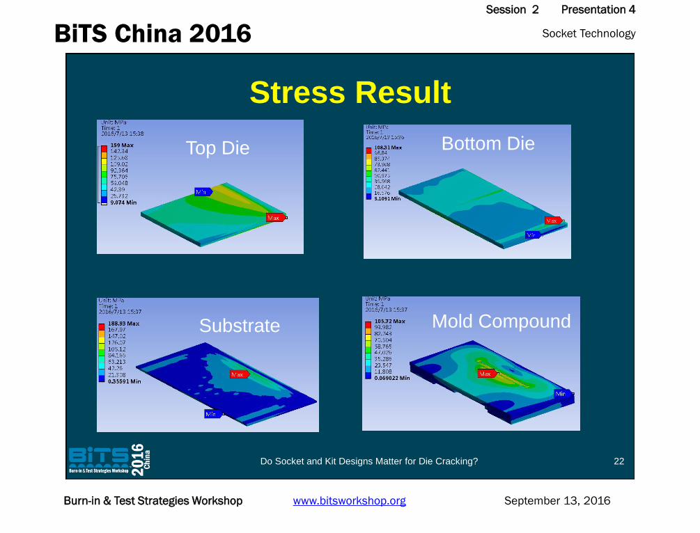
Case 3:
Load on Die edge.
Boundary Condition Setup
21Do Socket and Kit Designs Matter for Die Cracking?
Socket TechnologyBiTS China 2016Session 2 Presentation 4
September 13, 2016Burn-in & Test Strategies Workshop www.bitsworkshop.org
Top Die Bottom Die
Mold CompoundSubstrate
Stress Result
22Do Socket and Kit Designs Matter for Die Cracking?
Socket TechnologyBiTS China 2016Session 2 Presentation 4
September 13, 2016Burn-in & Test Strategies Workshop www.bitsworkshop.org
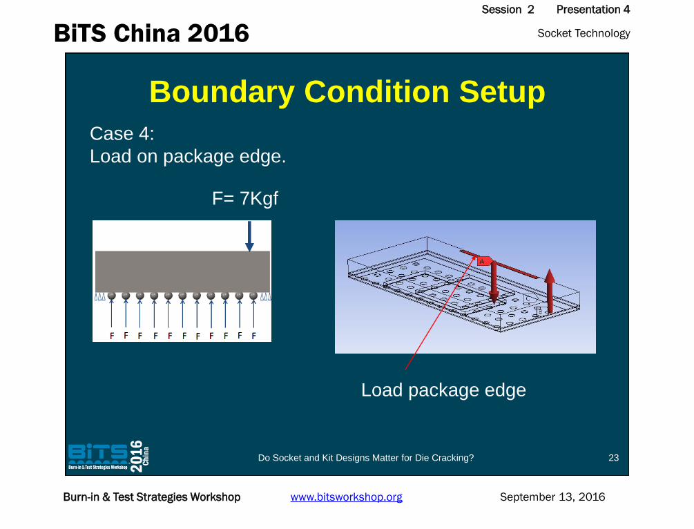
F= 7Kgf
Load package edge
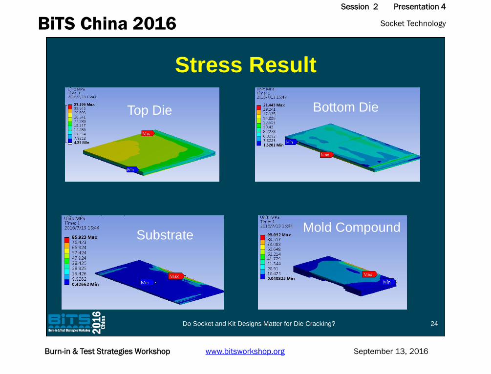
Case 4:
Load on package edge.
Boundary Condition Setup
23Do Socket and Kit Designs Matter for Die Cracking?
Socket TechnologyBiTS China 2016Session 2 Presentation 4
September 13, 2016Burn-in & Test Strategies Workshop www.bitsworkshop.org
Top Die Bottom Die
Mold CompoundSubstrate
Stress Result
24Do Socket and Kit Designs Matter for Die Cracking?

Socket TechnologyBiTS China 2016Session 2 Presentation 4
September 13, 2016Burn-in & Test Strategies Workshop www.bitsworkshop.org
• Load on Die edge and significant increase the stress
(Max:159 Mpa) for the Top die with 7 Kgf, which is near to
the silicon die tensile strength limit ,die maybe crack from
the load force position .
• Load on Package edge, far away Die edge; the load force
don’t load on die surface directly, can significant decrease
the stress (Max: 37.196 Mpa) for Top die.
• Compare with case 1,2,3,4, we can conclude that we
should avoided load force on die surface directly, can
decrease the die stress.
Result Analysis
25Do Socket and Kit Designs Matter for Die Cracking?
Socket TechnologyBiTS China 2016Session 2 Presentation 4
September 13, 2016Burn-in & Test Strategies Workshop www.bitsworkshop.org
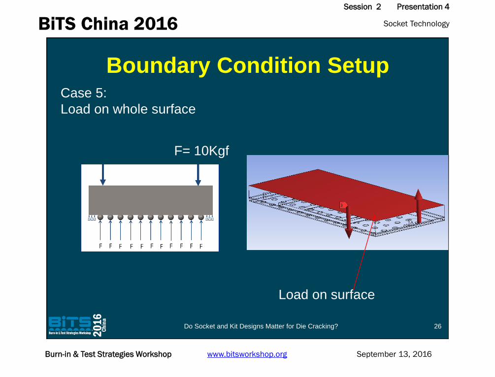
F= 10Kgf
Load on surface
Case 5:
Load on whole surface
Boundary Condition Setup
26Do Socket and Kit Designs Matter for Die Cracking?
Socket TechnologyBiTS China 2016Session 2 Presentation 4
September 13, 2016Burn-in & Test Strategies Workshop www.bitsworkshop.org
Top Die Bottom Die
Mold CompoundSubstrate
Stress Result
27Do Socket and Kit Designs Matter for Die Cracking?
Socket TechnologyBiTS China 2016Session 2 Presentation 4
September 13, 2016Burn-in & Test Strategies Workshop www.bitsworkshop.org
F= 10Kgf
Load on surface
Case 6:
Load on partial surface
Boundary Condition Setup
28Do Socket and Kit Designs Matter for Die Cracking?
Socket TechnologyBiTS China 2016Session 2 Presentation 4
September 13, 2016Burn-in & Test Strategies Workshop www.bitsworkshop.org
Top Die Bottom Die
Mold CompoundSubstrate
Stress Result
29Do Socket and Kit Designs Matter for Die Cracking?
Socket TechnologyBiTS China 2016Session 2 Presentation 4
September 13, 2016Burn-in & Test Strategies Workshop www.bitsworkshop.org
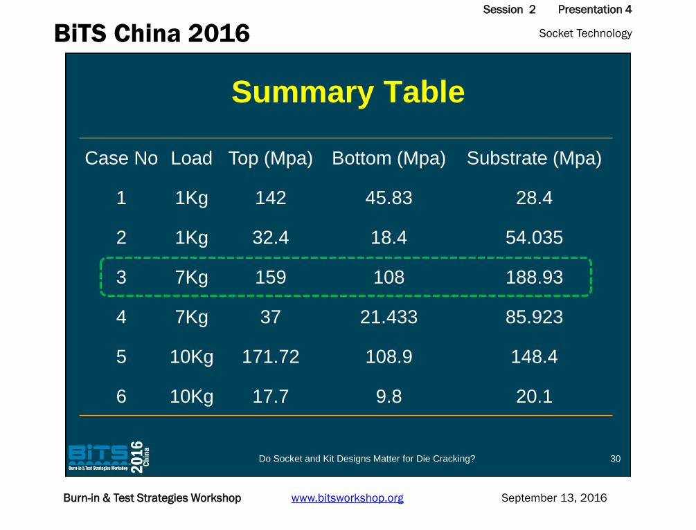
Summary Table
Case No Load Top (Mpa) Bottom (Mpa) Substrate (Mpa)
1 1Kg 142 45.83 28.4
2 1Kg 32.4 18.4 54.035
3 7Kg 159 108 188.93
4 7Kg 37 21.433 85.923
5 10Kg 171.72 108.9 148.4
6 10Kg 17.7 9.8 20.1
30Do Socket and Kit Designs Matter for Die Cracking?
Socket TechnologyBiTS China 2016Session 2 Presentation 4
September 13, 2016Burn-in & Test Strategies Workshop www.bitsworkshop.org
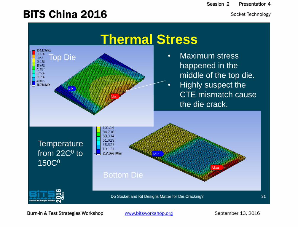
Thermal Stress
Top Die
Bottom Die
• Maximum stress
happened in the
middle of the top die.
• Highly suspect the
CTE mismatch cause
the die crack.
Temperature
from 22C0 to
150C0
31Do Socket and Kit Designs Matter for Die Cracking?
Socket TechnologyBiTS China 2016Session 2 Presentation 4
September 13, 2016Burn-in & Test Strategies Workshop www.bitsworkshop.org
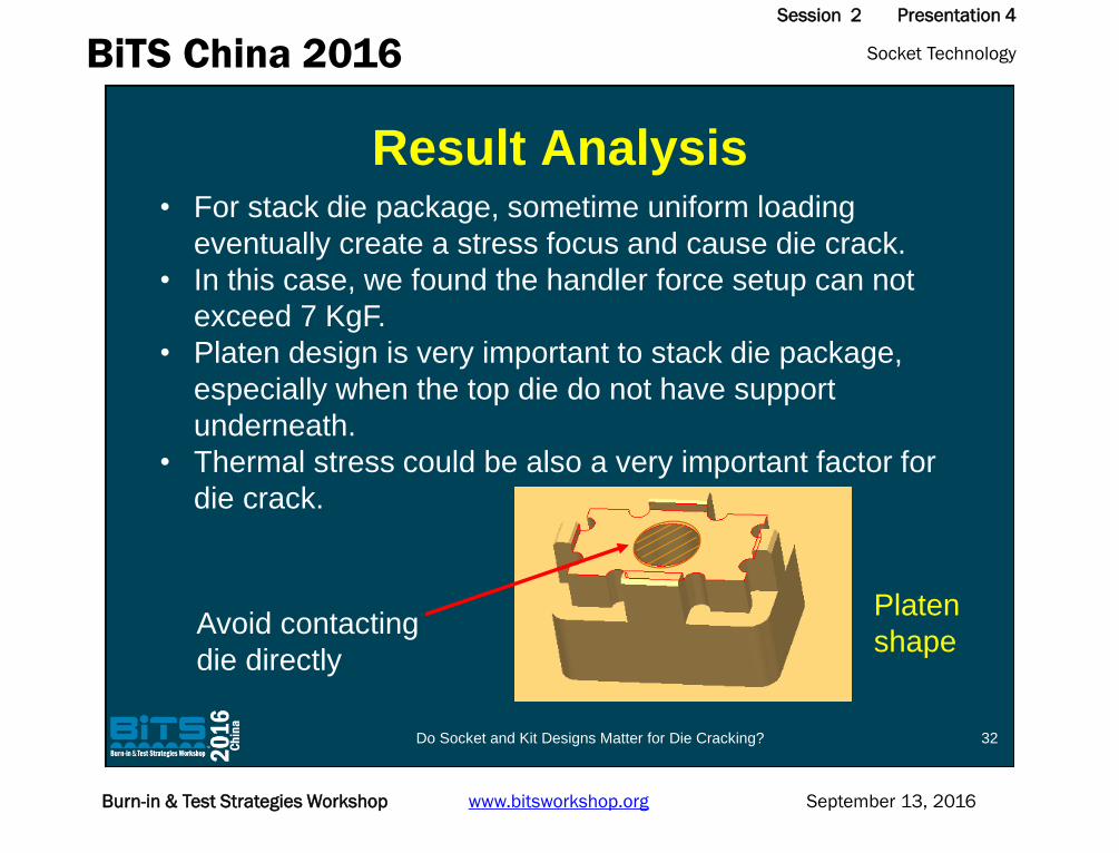
• For stack die package, sometime uniform loading
eventually create a stress focus and cause die crack.
• In this case, we found the handler force setup can not
exceed 7 KgF.
• Platen design is very important to stack die package,
especially when the top die do not have support
underneath.
• Thermal stress could be also a very important factor for
die crack.
Avoid contacting
die directly
Platen
shape
Result Analysis
32Do Socket and Kit Designs Matter for Die Cracking?