Embed Size (px)
Citation preview

1
SiGe(C) MOSFET Technology
Sanjay BanerjeeUniversity of Texas at Austin
� Issues in Scaled CMOS� Bandstructure, Transport and Strain� Enhanced Mobility Channels
- Strained Si and SiGe(C)� Multi-Gate and Novel MOSFETs� Process Integration Challenges
2
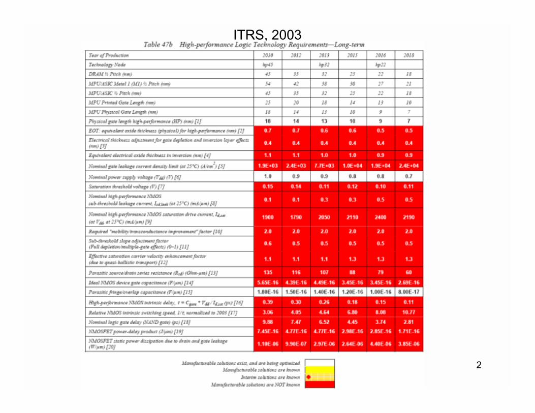
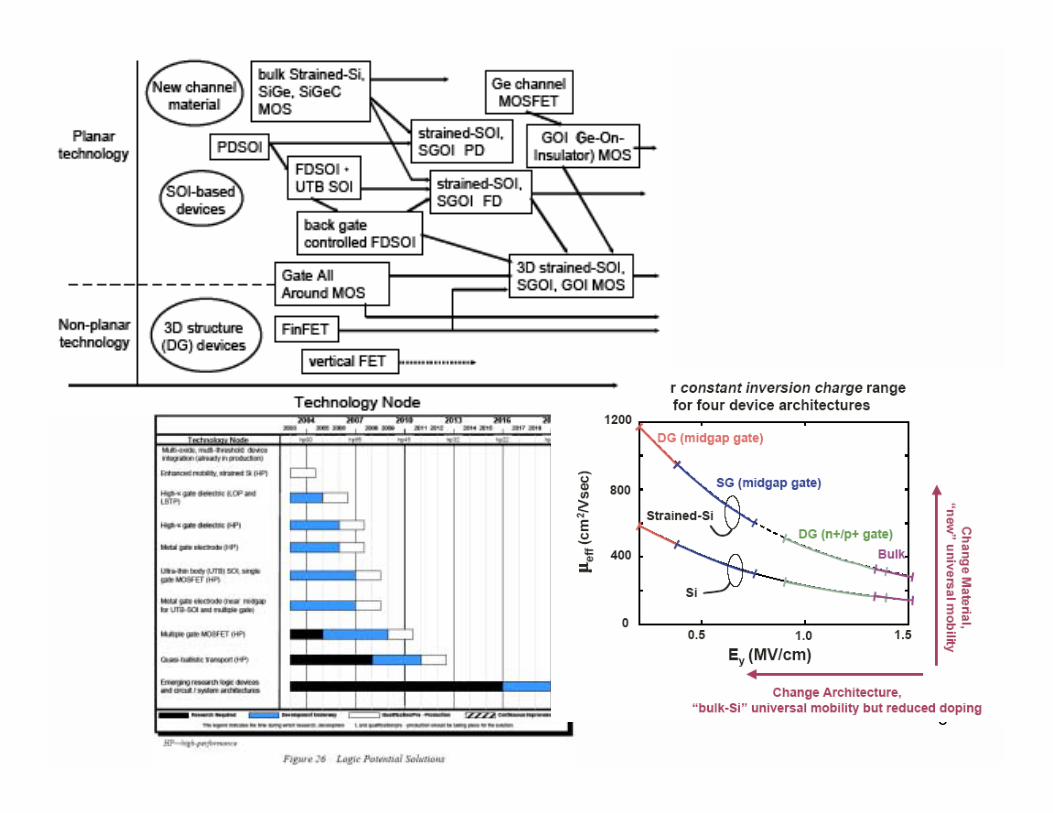
ITRS, 2003
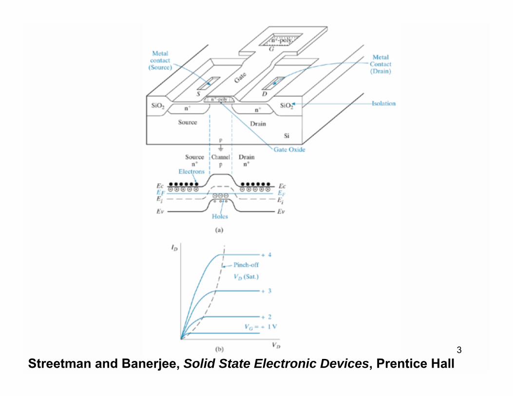
3Streetman and Banerjee, Solid State Electronic Devices, Prentice Hall
4
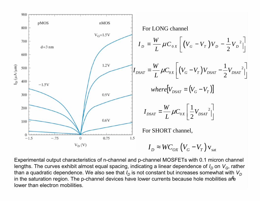
Experimental output characteristics of n-channel and p-channel MOSFETs with 0.1 micron channel lengths. The curves exhibit almost equal spacing, indicating a linear dependence of ID on VG, rather than a quadratic dependence. We also see that ID is not constant but increases somewhat with VDin the saturation region. The p-channel devices have lower currents because hole mobilities are lower than electron mobilities.
( ) 20
12D X G T D D
WI C V V V VL
µ = − −
( ) 20
12DSAT X G T DSAT DSAT
WI C V V V VL
µ = − −
( ) satvD OX G TI WC V V≈ −
For SHORT channel,
For LONG channel
20
12DSAT X DSAT
WI C VL
µ =
( )[ ]TGDSAT VVVwhere −=
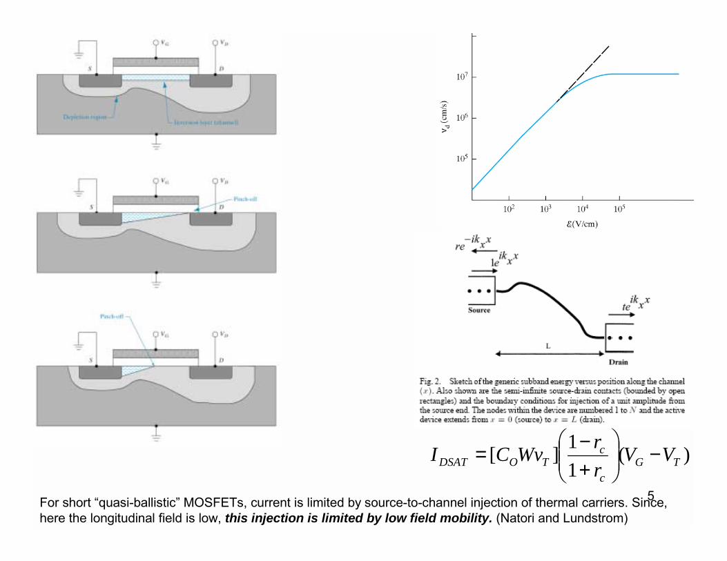
5For short �quasi-ballistic� MOSFETs, current is limited by source-to-channel injection of thermal carriers. Since, here the longitudinal field is low, this injection is limited by low field mobility. (Natori and Lundstrom)
)(11][ TG
c
cTODSAT VV
rrWvCI −
+−=
6
7
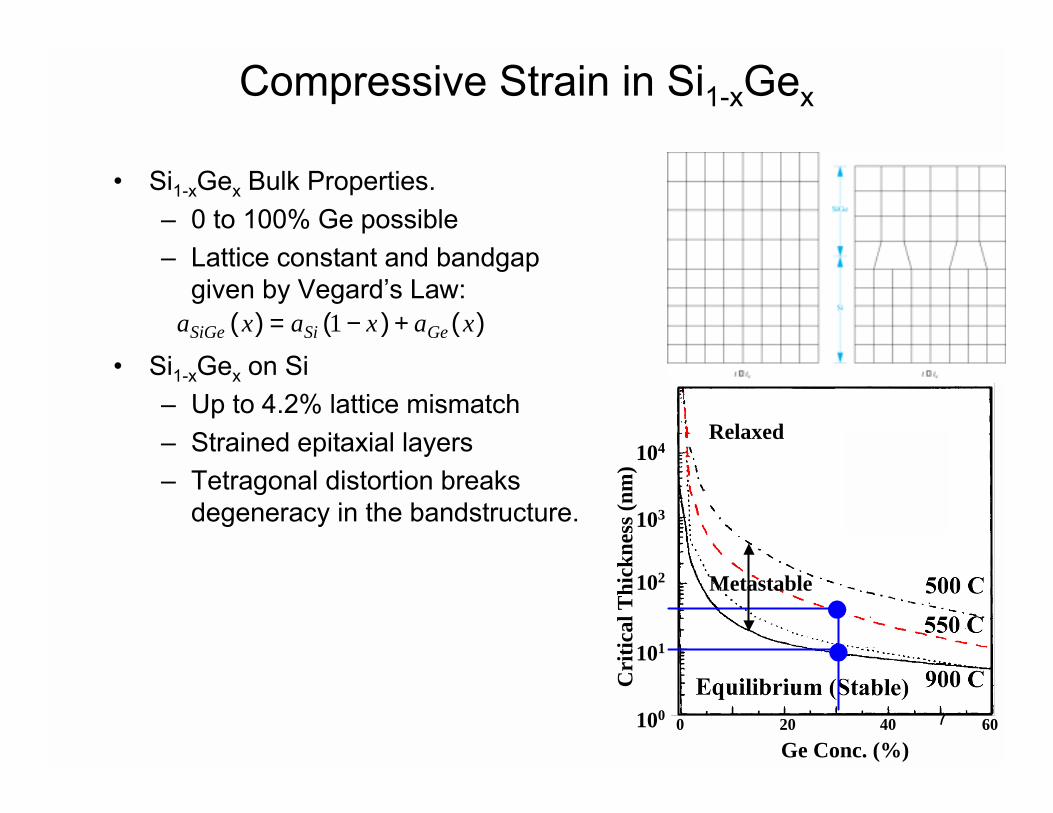
Compressive Strain in Si1-xGex
� Si1-xGex Bulk Properties.� 0 to 100% Ge possible� Lattice constant and bandgap
given by Vegard�s Law:
� Si1-xGex on Si� Up to 4.2% lattice mismatch� Strained epitaxial layers� Tetragonal distortion breaks
degeneracy in the bandstructure.
0 20 40 60100
101
102
103
104
Ge Conc. (%)
Cri
tical
Thi
ckne
ss (n
m)
Metastable
Relaxed
aSiGe x( ) = aSi 1 − x( ) + aGe x( )
8
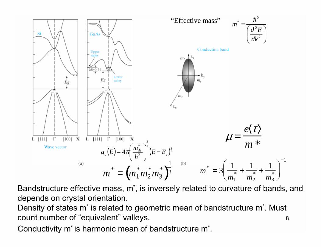
Bandstructure effective mass, m*, is inversely related to curvature of bands, and depends on crystal orientation.Density of states m* is related to geometric mean of bandstructure m*. Must count number of �equivalent� valleys.Conductivity m* is harmonic mean of bandstructure m*.
m* = 3 1m1
* + 1m2
* + 1m3
*
−1
µ =e τm *
m* = m1*m2
*m3*( )
13
( ) ( )212
3
2
*
4 cde
c EEhmEg −
= π
=
2
2
2*
dkEd
m !“Effective mass”
9
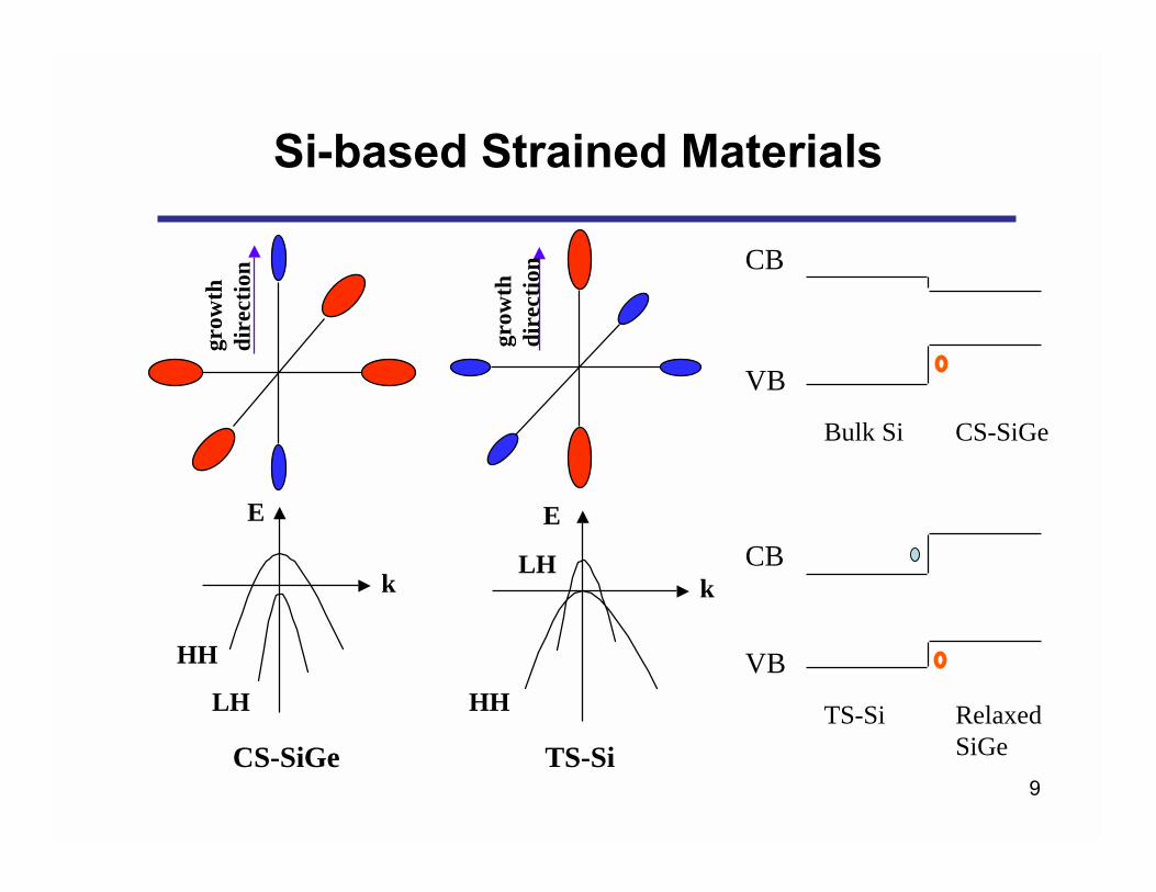
Si-based Strained Materials
grow
th
dire
ctio
nE
k
HH
LH
grow
th
dire
ctio
n
E
k
HH
LH
CB
Bulk Si CS-SiGe
VB
CB
TS-Si Relaxed SiGe
VB
CS-SiGe TS-Si
10
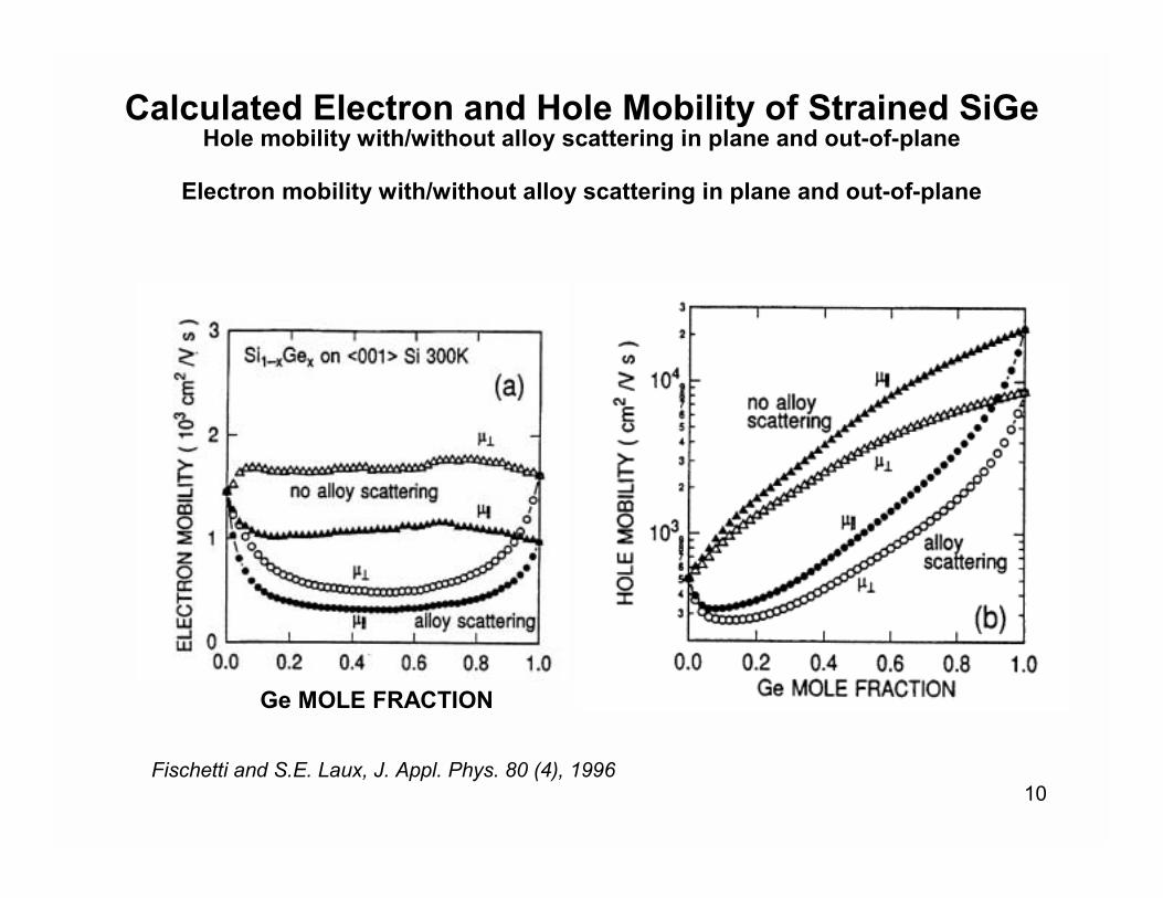
Calculated Electron and Hole Mobility of Strained SiGeHole mobility with/without alloy scattering in plane and out-of-plane
Electron mobility with/without alloy scattering in plane and out-of-plane
Ge MOLE FRACTION
Fischetti and S.E. Laux, J. Appl. Phys. 80 (4), 1996
11
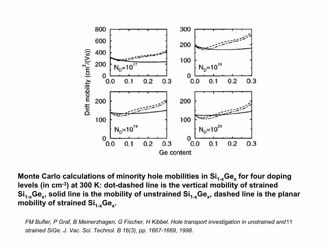
Monte Carlo calculations of minority hole mobilities in Si1-xGex for four doping levels (in cm-3) at 300 K: dot-dashed line is the vertical mobility of strained Si1-xGex, solid line is the mobility of unstrained Si1-xGex, dashed line is the planar mobility of strained Si1-xGex.
FM Bufler, P Graf, B Meinerzhagen, G Fischer, H Kibbel. Hole transport investigation in unstrained and strained SiGe. J. Vac. Sci. Technol. B 16(3), pp. 1667-1669, 1998.
12
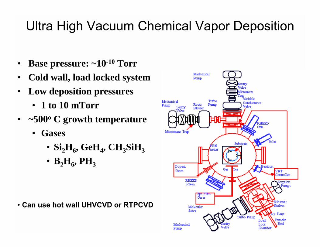
• Base pressure: ~10-10 Torr• Cold wall, load locked system• Low deposition pressures
• 1 to 10 mTorr• ~500o C growth temperature
• Gases• Si2H6, GeH4, CH3SiH3
• B2H6, PH3
Ultra High Vacuum Chemical Vapor Deposition
� Can use hot wall UHVCVD or RTPCVD
13
14
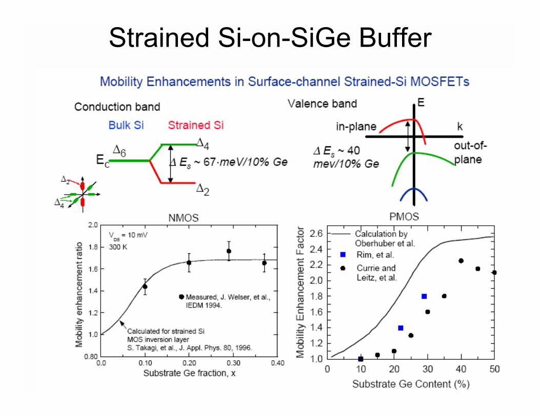
Strained Si-on-SiGe Buffer
15
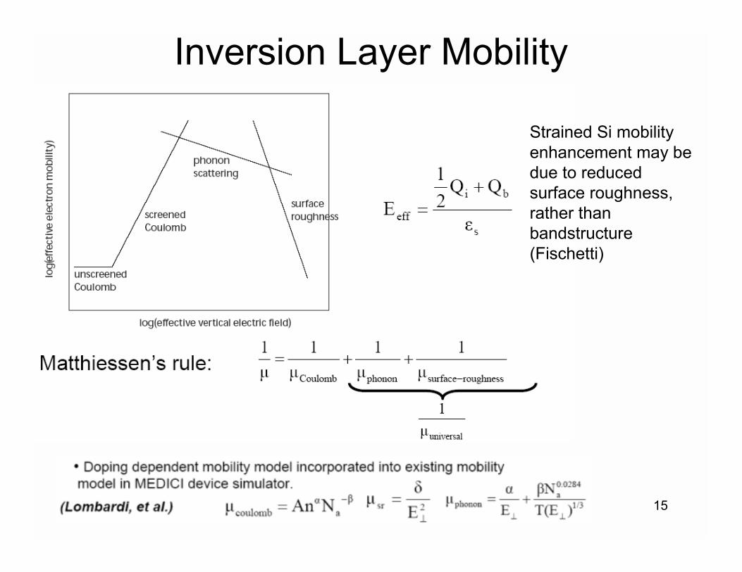
Inversion Layer Mobility
Strained Si mobility enhancement may be due to reduced surface roughness, rather than bandstructure(Fischetti)
16
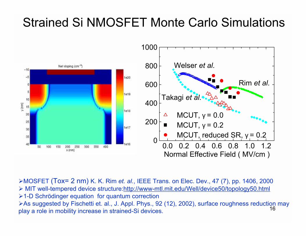
Strained Si NMOSFET Monte Carlo Simulations
0.0 0.2 0.4 0.6 0.8 1.0 1.20
200
400
600
800
1000
MCUT, γ = 0.0 MCUT, γ = 0.2 MCUT, reduced SR, γ = 0.2
Takagi et al.
Rim et al.
Welser et al.
Normal Effective Field ( MV/cm )
!MOSFET (Tox= 2 nm) K. K. Rim et. al., IEEE Trans. on Elec. Dev., 47 (7), pp. 1406, 2000! MIT well-tempered device structure:http://www-mtl.mit.edu/Well/device50/topology50.html!1-D Schrödinger equation for quantum correction!As suggested by Fischetti et. al., J. Appl. Phys., 92 (12), 2002), surface roughness reduction may play a role in mobility increase in strained-Si devices.
17
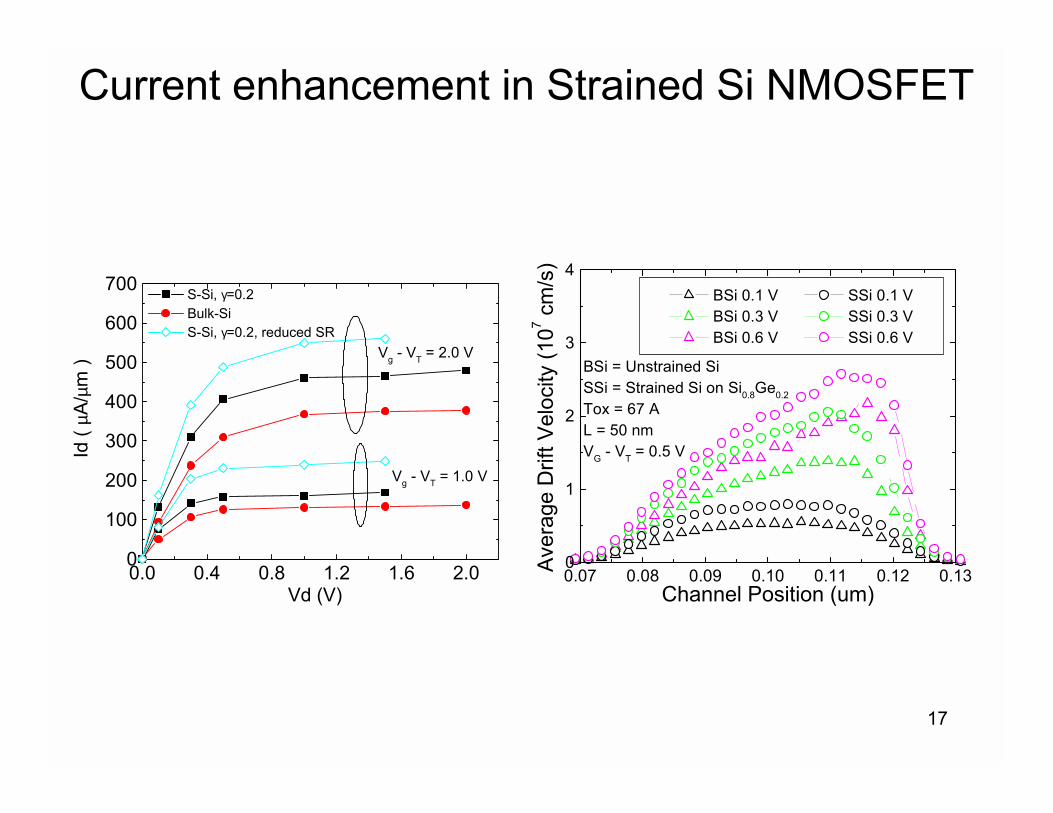
Current enhancement in Strained Si NMOSFET
0.0 0.4 0.8 1.2 1.6 2.00
100
200
300
400
500
600
700 S-Si, γ=0.2 Bulk-Si S-Si, γ=0.2, reduced SR
Vg - VT = 1.0 V
Vg - VT = 2.0 V
Id (
µA/µ
m )
Vd (V)0.07 0.08 0.09 0.10 0.11 0.12 0.130
1
2
3
4
BSi = Unstrained SiSSi = Strained Si on Si0.8Ge0.2
Tox = 67 AL = 50 nmVG - VT = 0.5 V
Channel Position (um)
Ave
rage
Drif
t Vel
ocity
(107 c
m/s
)
BSi 0.1 V SSi 0.1 V BSi 0.3 V SSi 0.3 V BSi 0.6 V SSi 0.6 V
18
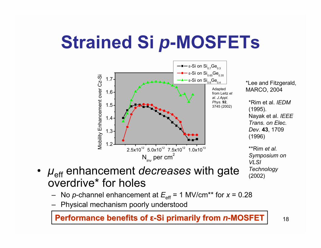
Strained Si p-MOSFETs
� µeff enhancement decreases with gate overdrive* for holes� No p-channel enhancement at Eeff = 1 MV/cm** for x = 0.28� Physical mechanism poorly understood
2.5x10¹² 5.0x10¹² 7.5x10¹² 1.0x10131.2
1.3
1.4
1.5
1.6
1.7
Mob
ility
Enh
ance
men
t ove
r Cz-
Si
Ninv per cm2
ε-Si on Si0.7Ge0.3
ε-Si on Si0.65Ge0.35
ε-Si on Si0.6Ge0.4
**Rim et al.Symposium on VLSI Technology(2002)
Performance benefits of Performance benefits of εε--Si Si primarilyprimarily from from nn--MOSFETMOSFET
Adapted from Leitz et al. J.Appl. Phys. 92, 3745 (2002)
*Rim et al. IEDM(1995).Nayak et al. IEEE Trans. on Elec. Dev. 43, 1709 (1996)
*Lee and Fitzgerald, MARCO, 2004
19
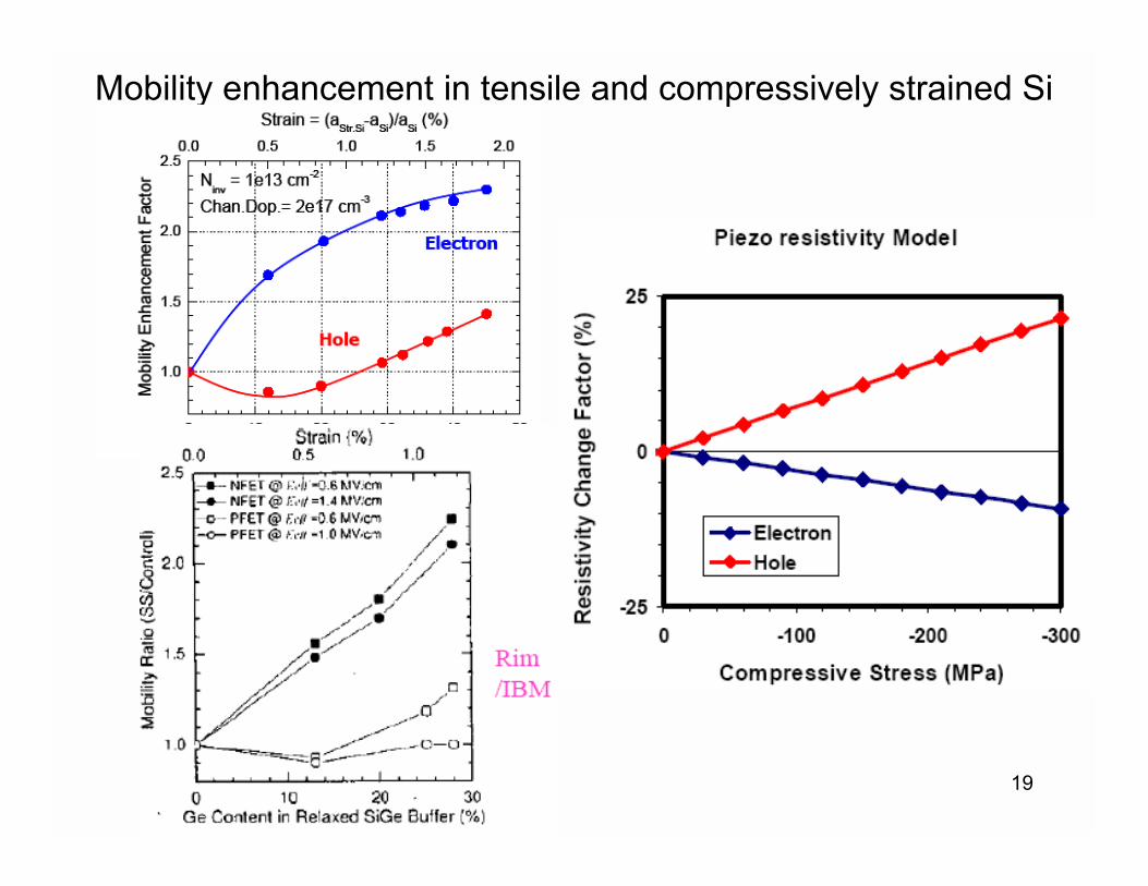
Mobility enhancement in tensile and compressively strained Si
20
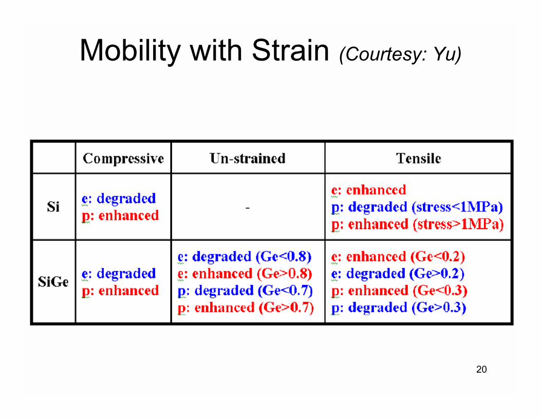
Mobility with Strain (Courtesy: Yu)
21
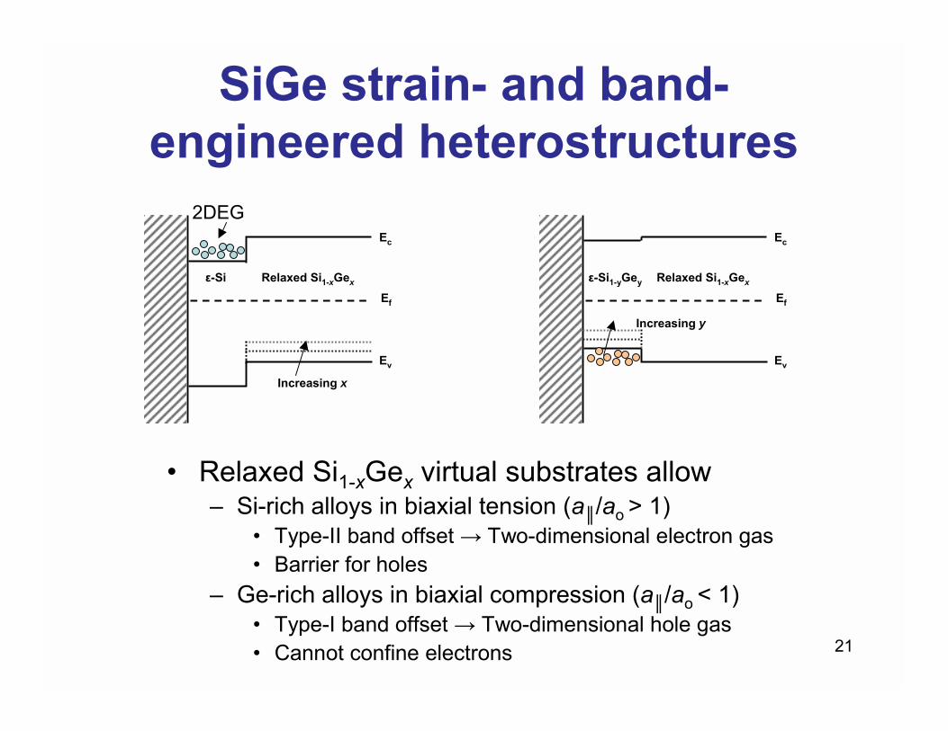
SiGe strain- and band-engineered heterostructures
� Relaxed Si1-xGex virtual substrates allow � Si-rich alloys in biaxial tension (a║/ao > 1)
� Type-II band offset → Two-dimensional electron gas� Barrier for holes
� Ge-rich alloys in biaxial compression (a║/ao < 1)� Type-I band offset → Two-dimensional hole gas� Cannot confine electrons
Relaxed Si1-xGex
Ec
Ef
Ev
ε-Si
Increasing x
2DEG
Relaxed Si1-xGex
Ec
Ef
Ev
ε-Si1-yGey
Increasing y
22
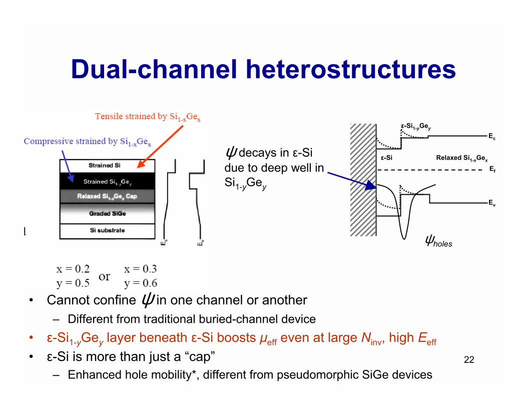
Dual-channel heterostructures
� Cannot confine ψ in one channel or another� Different from traditional buried-channel device
� ε-Si1-yGey layer beneath ε-Si boosts µeff even at large Ninv, high Eeff
� ε-Si is more than just a �cap�� Enhanced hole mobility*, different from pseudomorphic SiGe devices
Relaxed Si1-xGex
Ec
Ef
Ev
ε-Si
ε-Si1-yGey
ψholes
ψ decays in ε-Si due to deep well in Si1-yGey
23
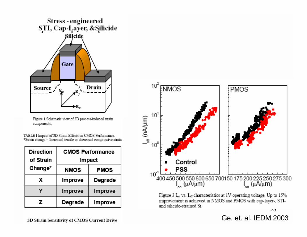
Ge, et. al, IEDM 2003
24
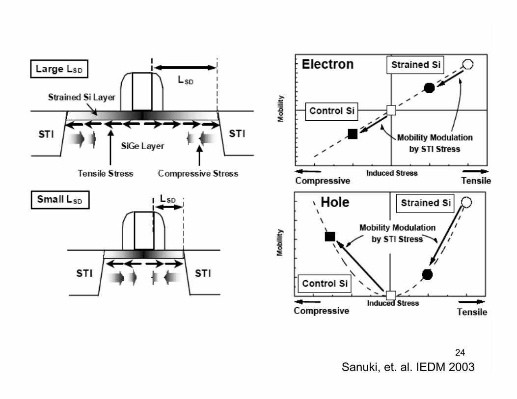
Sanuki, et. al. IEDM 2003
25
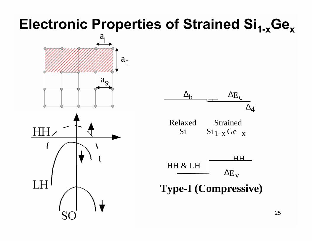
Electronic Properties of Strained Si1-xGex
HH & LHHH
∆Ev
∆Ec∆4
∆6
RelaxedSi
StrainedSi 1-x Ge x
Type-I (Compressive)
a||
a⊥
aSi
26
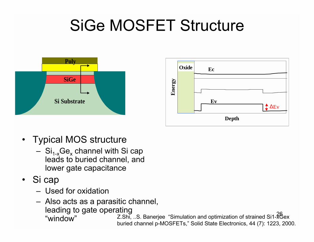
SiGe MOSFET Structure
� Typical MOS structure� Si1-xGex channel with Si cap
leads to buried channel, and lower gate capacitance
� Si cap� Used for oxidation� Also acts as a parasitic channel,
leading to gate operating �window�
Poly
SiGe
Si Substrate
Depth
Ene
rgy
Ec
Ev
Oxide
∆Ev
Z.Shi, ..S. Banerjee �Simulation and optimization of strained Si1-xGex buried channel p-MOSFETs,� Solid State Electronics, 44 (7): 1223, 2000.
27
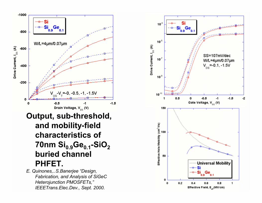
Output, sub-threshold, and mobility-field characteristics of 70nm Si0.9Ge0.1-SiO2buried channel PHFET.
E. Quinones,..S.Banerjee �Design, Fabrication, and Analysis of SiGeCHeterojunction PMOSFETs,� IEEETrans.Elec.Dev., Sept. 2000.
28
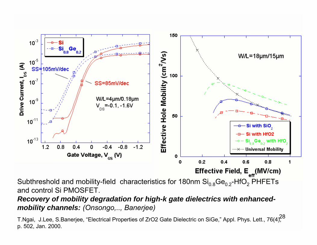
Subthreshold and mobility-field characteristics for 180nm Si0.8Ge0.2-HfO2 PHFETsand control Si PMOSFET. Recovery of mobility degradation for high-k gate dielectrics with enhanced-mobility channels: (Onsongo,.., Banerjee)T.Ngai, J.Lee, S.Banerjee, �Electrical Properties of ZrO2 Gate Dielectric on SiGe,� Appl. Phys. Lett., 76(4), p. 502, Jan. 2000.
29
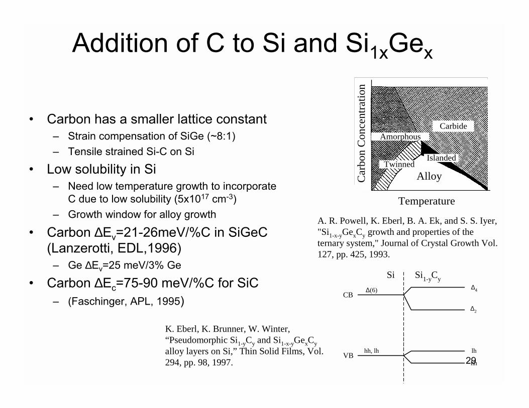
Addition of C to Si and Si1xGex
� Carbon has a smaller lattice constant� Strain compensation of SiGe (~8:1)� Tensile strained Si-C on Si
� Low solubility in Si� Need low temperature growth to incorporate
C due to low solubility (5x1017 cm-3)� Growth window for alloy growth
� Carbon ∆Ev=21-26meV/%C in SiGeC (Lanzerotti, EDL,1996)
� Ge ∆Ev=25 meV/3% Ge
� Carbon ∆Ec=75-90 meV/%C for SiC � (Faschinger, APL, 1995)
Si Si1-yCy
∆(6) ∆4
∆2
hh, lh lh
hh
CB
VB
Alloy
CarbideAmorphous
TwinnedIslanded
Temperature
Car
bon
Con
cent
ratio
n
A. R. Powell, K. Eberl, B. A. Ek, and S. S. Iyer, "Si1-x-yGexCy growth and properties of the ternary system," Journal of Crystal Growth Vol. 127, pp. 425, 1993.
K. Eberl, K. Brunner, W. Winter, “Pseudomorphic Si1-yCy and Si1-x-yGexCyalloy layers on Si,” Thin Solid Films, Vol. 294, pp. 98, 1997.
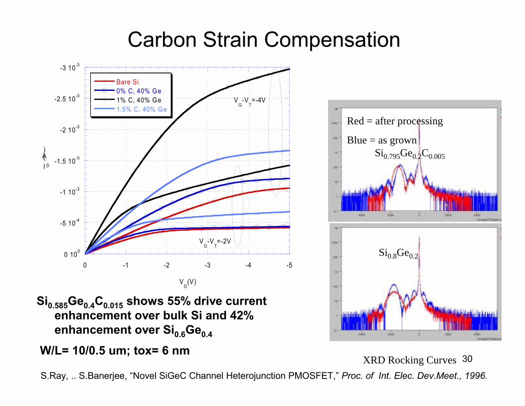
30
Carbon Strain Compensation
Red = after processing
Blue = as grownSi0.795Ge0.2C0.005
Si0.8Ge0.2
XRD Rocking Curves
-3 10-3
-2.5 10-3
-2 10-3
-1.5 10-3
-1 10-3
-5 10-4
0 100
-5-4-3-2-10
Bare Si0% C, 40% Ge1% C, 40% Ge1.5% C, 40% Ge
I D (A)
VD(V)
VG
-VT=-4V
VG
-VT=-2V
Si0.585Ge0.4C0.015 shows 55% drive current enhancement over bulk Si and 42% enhancement over Si0.6Ge0.4
W/L= 10/0.5 um; tox= 6 nm
S.Ray, .. S.Banerjee, �Novel SiGeC Channel Heterojunction PMOSFET,� Proc. of Int. Elec. Dev.Meet., 1996.
31
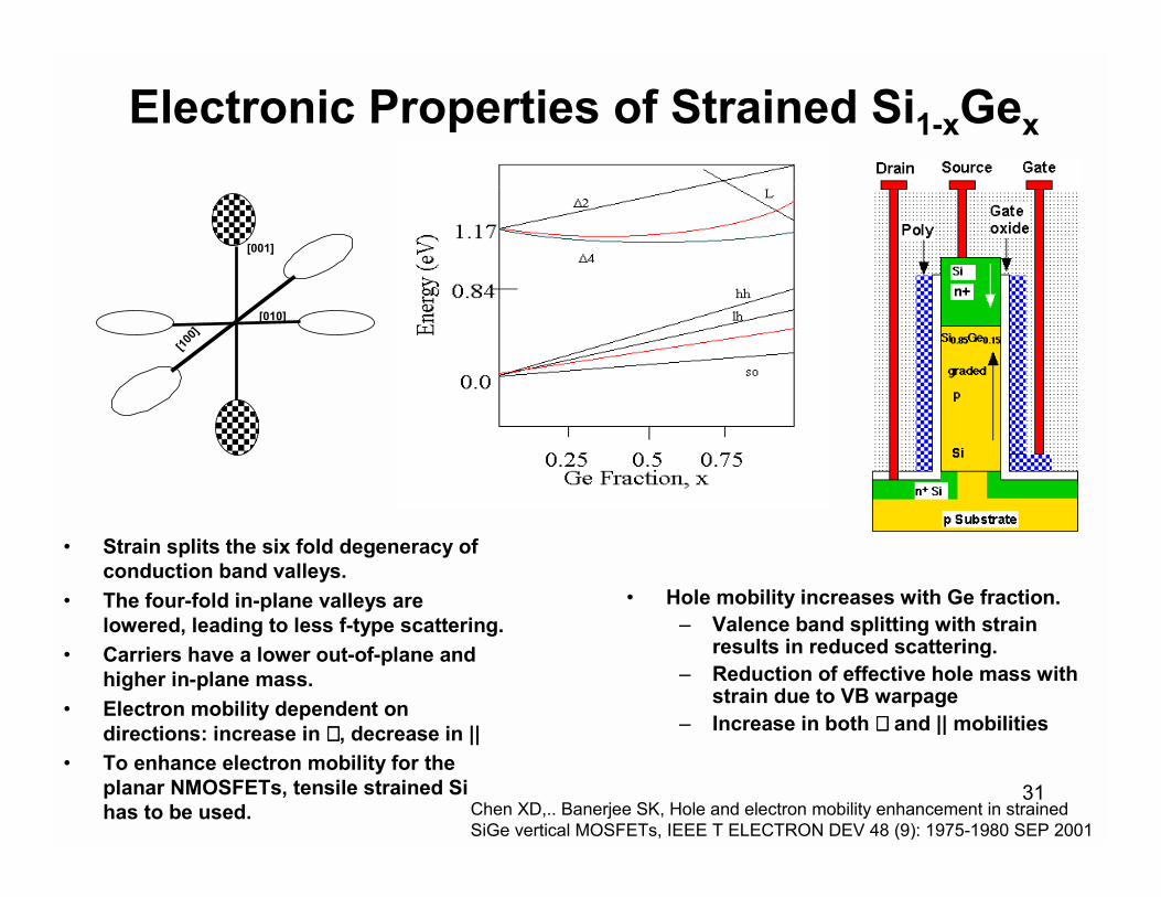
Electronic Properties of Strained Si1-xGex
� Strain splits the six fold degeneracy of conduction band valleys.
� The four-fold in-plane valleys are lowered, leading to less f-type scattering.
� Carriers have a lower out-of-plane and higher in-plane mass.
� Electron mobility dependent on directions: increase in ⊥⊥⊥⊥ , decrease in ||
� To enhance electron mobility for the planar NMOSFETs, tensile strained Sihas to be used.
[001]
[010]
[100]
� Hole mobility increases with Ge fraction.� Valence band splitting with strain
results in reduced scattering.� Reduction of effective hole mass with
strain due to VB warpage� Increase in both ⊥⊥⊥⊥ and || mobilities
Chen XD,.. Banerjee SK, Hole and electron mobility enhancement in strained SiGe vertical MOSFETs, IEEE T ELECTRON DEV 48 (9): 1975-1980 SEP 2001
32
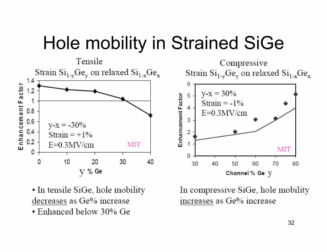
Hole mobility in Strained SiGe
33
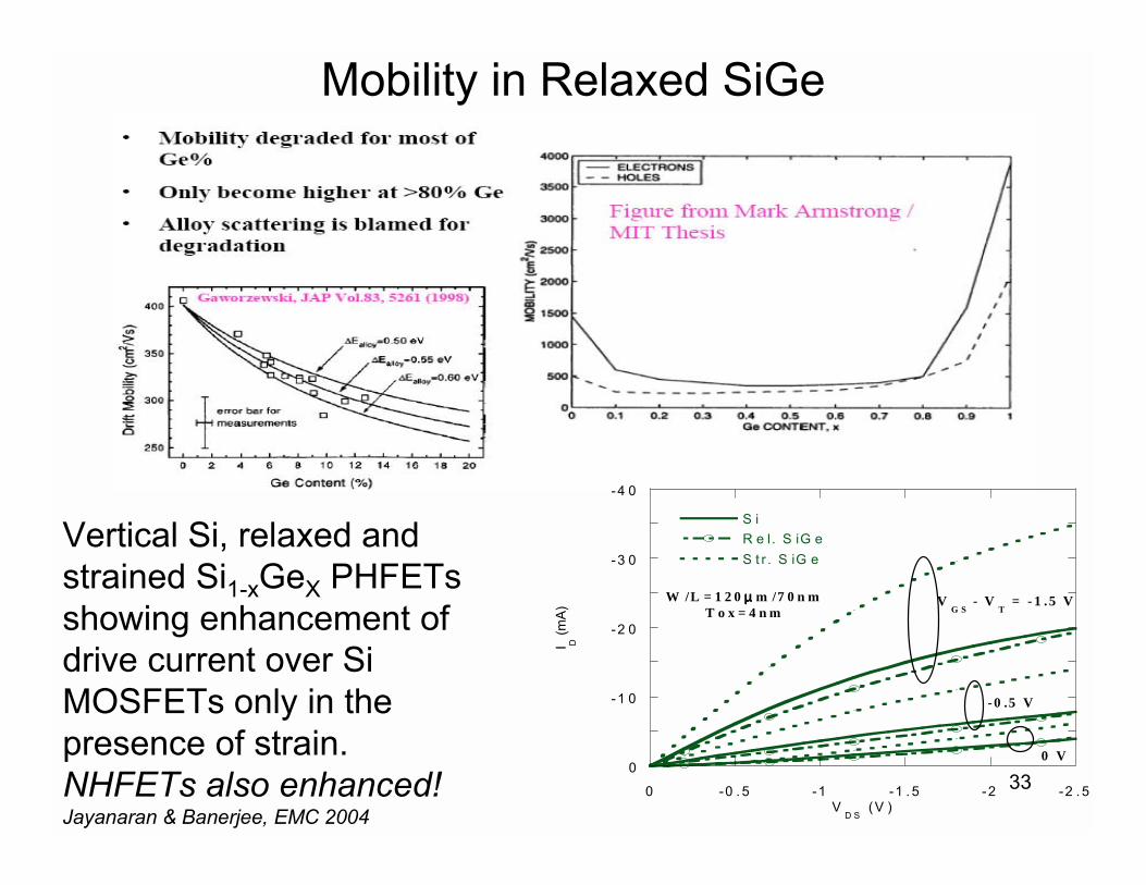
Mobility in Relaxed SiGe
-4 0
-3 0
-2 0
-1 0
0
-2 . 5-2-1 . 5-1-0 . 50
S iR e l. S iG eS t r . S iG e
I D (m
A)
VD S
(V )
VG S
- VT
= - 1 .5 V
- 0 .5 V
0 V
W /L = 1 2 0 µµµµ m /7 0 n mT o x = 4 n m
Vertical Si, relaxed and strained Si1-xGeX PHFETsshowing enhancement of drive current over SiMOSFETs only in the presence of strain. NHFETs also enhanced! Jayanaran & Banerjee, EMC 2004
34
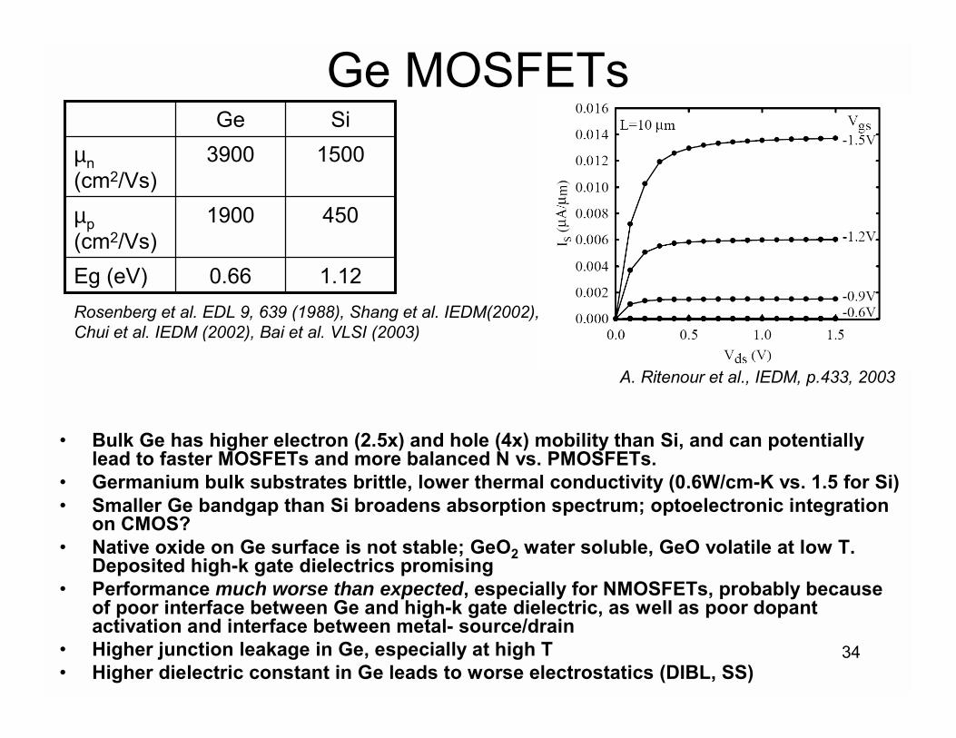
Ge MOSFETs
� Bulk Ge has higher electron (2.5x) and hole (4x) mobility than Si, and can potentially lead to faster MOSFETs and more balanced N vs. PMOSFETs.
� Germanium bulk substrates brittle, lower thermal conductivity (0.6W/cm-K vs. 1.5 for Si)� Smaller Ge bandgap than Si broadens absorption spectrum; optoelectronic integration
on CMOS?� Native oxide on Ge surface is not stable; GeO2 water soluble, GeO volatile at low T.
Deposited high-k gate dielectrics promising� Performance much worse than expected, especially for NMOSFETs, probably because
of poor interface between Ge and high-k gate dielectric, as well as poor dopantactivation and interface between metal- source/drain
� Higher junction leakage in Ge, especially at high T� Higher dielectric constant in Ge leads to worse electrostatics (DIBL, SS)
1.120.66Eg (eV)
4501900µp(cm2/Vs)
15003900µn(cm2/Vs)
SiGe
A. Ritenour et al., IEDM, p.433, 2003
Rosenberg et al. EDL 9, 639 (1988), Shang et al. IEDM(2002), Chui et al. IEDM (2002), Bai et al. VLSI (2003)
35
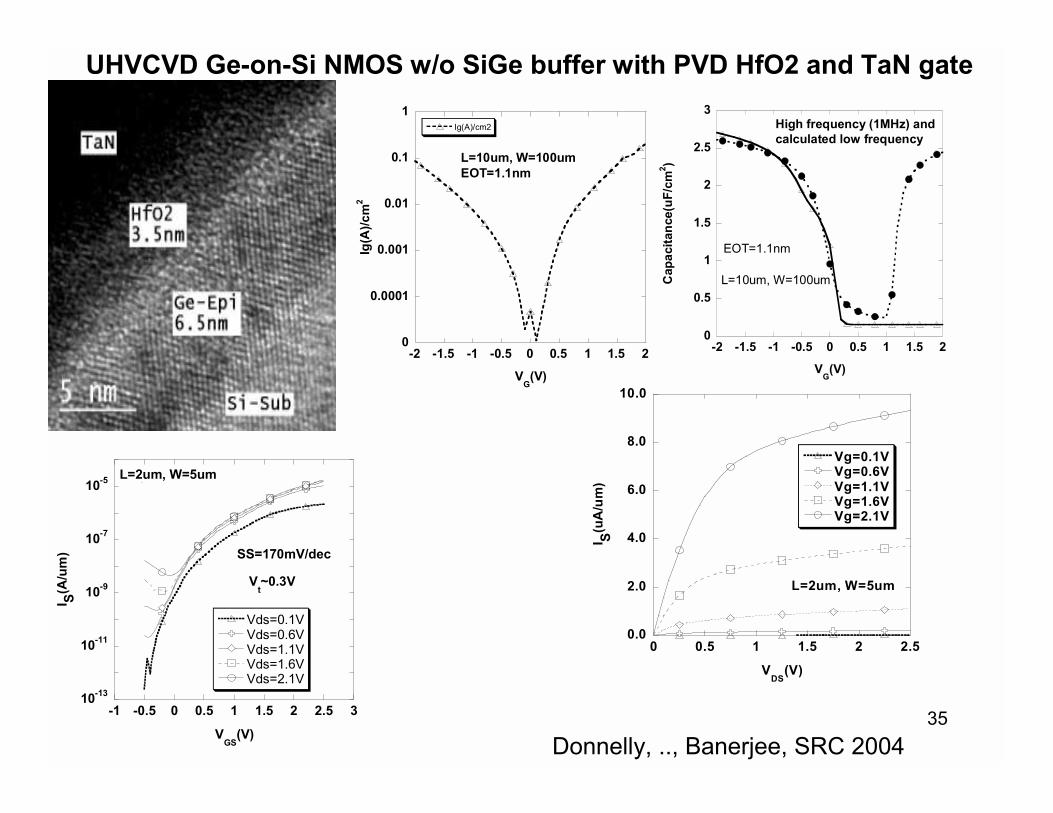
UHVCVD Ge-on-Si NMOS w/o SiGe buffer with PVD HfO2 and TaN gate
0
0.5
1
1.5
2
2.5
3
-2 -1.5 -1 -0.5 0 0.5 1 1.5 2
Cap
acita
nce(
uF/c
m2 )
VG(V)
EOT=1.1nm
L=10um, W=100um
High frequency (1MHz) andcalculated low frequency
10-13
10-11
10-9
10-7
10-5
-1 -0.5 0 0.5 1 1.5 2 2.5 3
Vds=0.1VVds=0.6VVds=1.1VVds=1.6VVds=2.1V
I S(A/u
m)
VGS
(V)
L=2um, W=5um
SS=170mV/dec
Vt~0.3V
0
0.0001
0.001
0.01
0.1
1
-2 -1.5 -1 -0.5 0 0.5 1 1.5 2
Ig(A)/cm2
Ig(A
)/cm
2
VG(V)
L=10um, W=100umEOT=1.1nm
0.0
2.0
4.0
6.0
8.0
10.0
0 0.5 1 1.5 2 2.5
Vg=0.1VVg=0.6VVg=1.1VVg=1.6VVg=2.1V
I S(uA
/um
)
VDS
(V)
L=2um, W=5um
Donnelly, .., Banerjee, SRC 2004
36
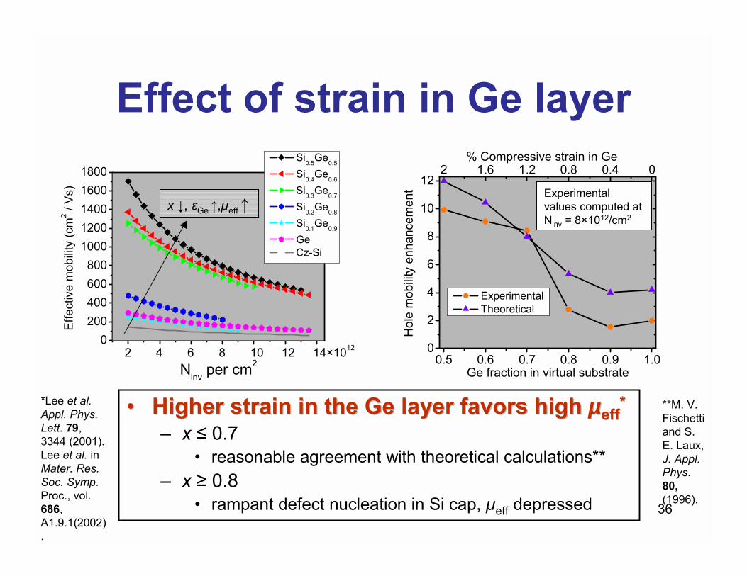
Effect of strain in Ge layer
2 4 6 8 10 12 14×10120
200400600800
10001200140016001800
Effe
ctiv
e m
obilit
y (c
m2 /
Vs)
Ninv per cm2
Si0.5Ge0.5
Si0.4Ge0.6
Si0.3Ge0.7
Si0.2Ge0.8
Si0.1Ge0.9
Ge Cz-Si
�� Higher strain in the Ge layer favors high Higher strain in the Ge layer favors high µµeffeff**
� x ≤ 0.7� reasonable agreement with theoretical calculations**
� x ≥ 0.8 � rampant defect nucleation in Si cap, µeff depressed
x ↓, εGe ↑,µeff ↑
**M. V. Fischettiand S. E. Laux, J. Appl. Phys. 80,(1996).
0.5 0.6 0.7 0.8 0.9 1.00
2
4
6
8
10
122 1.6 1.2 0.8 0.4 0
Hol
e m
obilit
y en
hanc
emen
t
Ge fraction in virtual substrate
Experimental Theoretical
% Compressive strain in Ge
Experimental values computed at Ninv = 8×10¹²/cm2
*Lee et al. Appl. Phys. Lett. 79, 3344 (2001). Lee et al. inMater. Res. Soc. Symp. Proc., vol. 686, A1.9.1(2002).
37
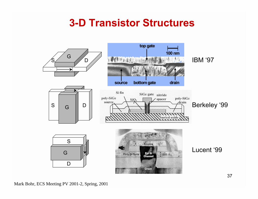
3-D Transistor Structures
S
G
D
S DG
S G D
source
top gate
bottom gate drain
100 nmIBM �97
Berkeley �99
Lucent �99
Mark Bohr, ECS Meeting PV 2001-2, Spring, 2001
38
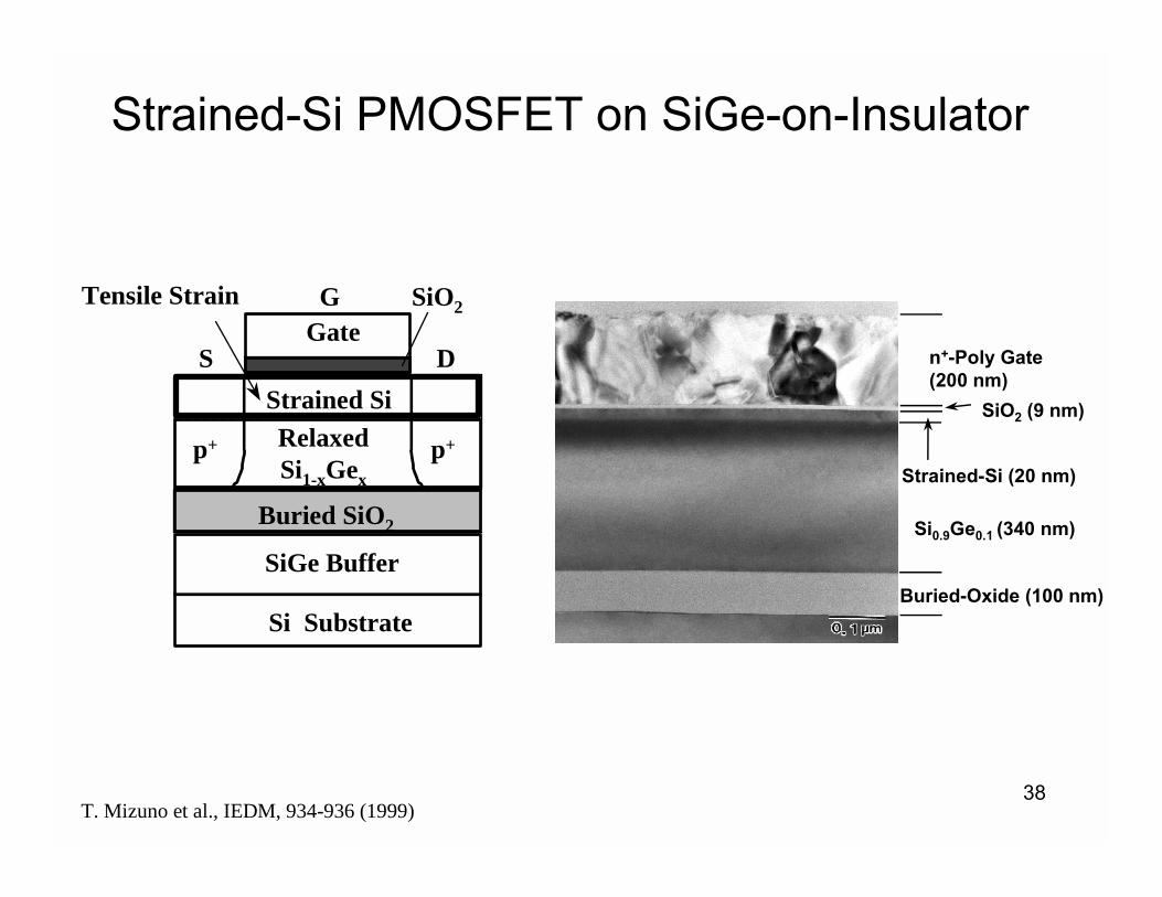
Si0.9Ge0.1 (340 nm)
Buried-Oxide (100 nm)
Strained-Si (20 nm)
SiO2 (9 nm)
n+-Poly Gate(200 nm)
Strained-Si PMOSFET on SiGe-on-Insulator
T. Mizuno et al., IEDM, 934-936 (1999)
Strained SiRelaxedSi1-xGex
SiGe Buffer
Si Substrate
Gate
p+ p+
SiO2
S
G
D
Tensile Strain
Buried SiO2
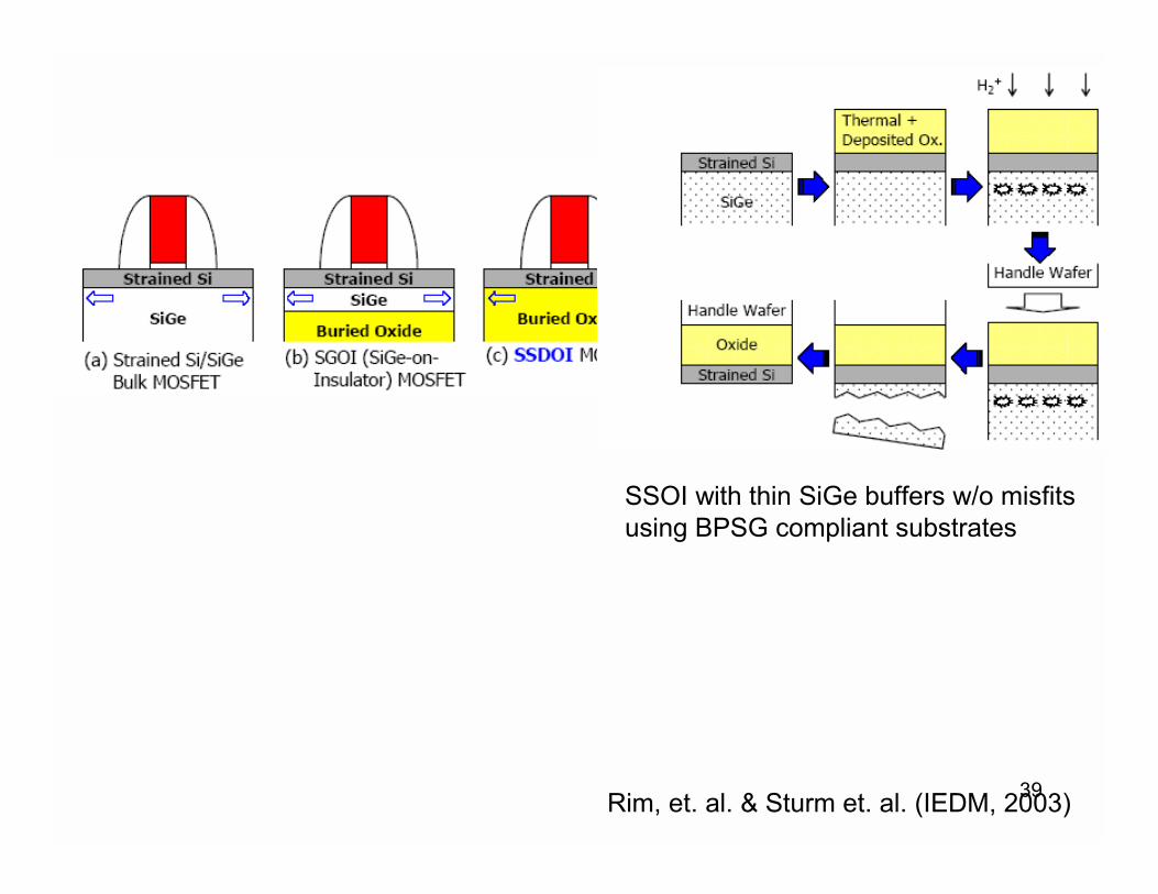
39Rim, et. al. & Sturm et. al. (IEDM, 2003)
SSOI with thin SiGe buffers w/o misfits using BPSG compliant substrates
40
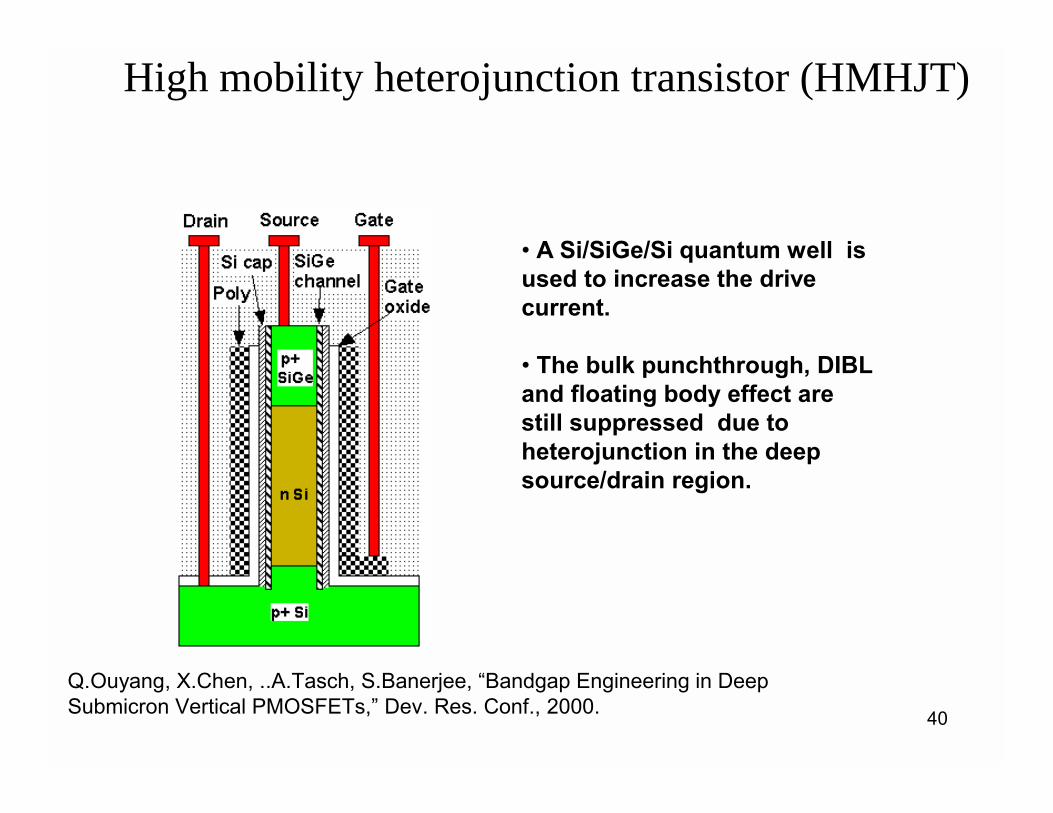
High mobility heterojunction transistor (HMHJT)
� A Si/SiGe/Si quantum well is used to increase the drive current.
� The bulk punchthrough, DIBL and floating body effect are still suppressed due to heterojunction in the deep source/drain region.
Q.Ouyang, X.Chen, ..A.Tasch, S.Banerjee, �Bandgap Engineering in Deep Submicron Vertical PMOSFETs,� Dev. Res. Conf., 2000.
41
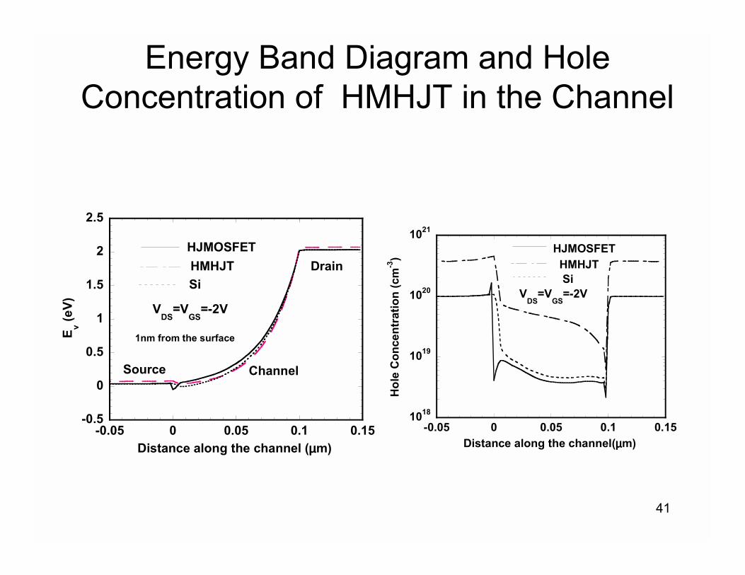
Energy Band Diagram and Hole Concentration of HMHJT in the Channel
-0.5
0
0.5
1
1.5
2
2.5
-0.05 0 0.05 0.1 0.15
E v (eV)
Distance along the channel (µµµµm)
HJMOSFETHMHJTSi
VDS
=VGS
=-2V
1nm from the surface
Source Channel
Drain
1018
1019
1020
1021
-0.05 0 0.05 0.1 0.15
Hol
e C
once
ntra
tion
(cm
-3)
Distance along the channel(µµµµm)
HJMOSFETHMHJTSi
VDS
=VGS
=-2V
42
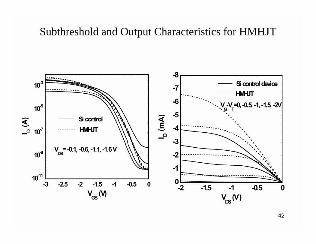
Subthreshold and Output Characteristics for HMHJT
10-11
10-9
10-7
10-5
10-3
-3 -2.5 -2 -1.5 -1 -0.5 0
I D (A
)
VGS
(V)
Si controlHMHJT
VDS
= -0.1, -0.6, -1.1, -1.6 V
-8
-7
-6
-5
-4
-3
-2
-1
0-2 -1.5 -1 -0.5 0
I D (m
A)
VDS
(V )
Si control deviceHMHJT
VG-V
T=0, -0.5, -1, -1.5, -2V
43
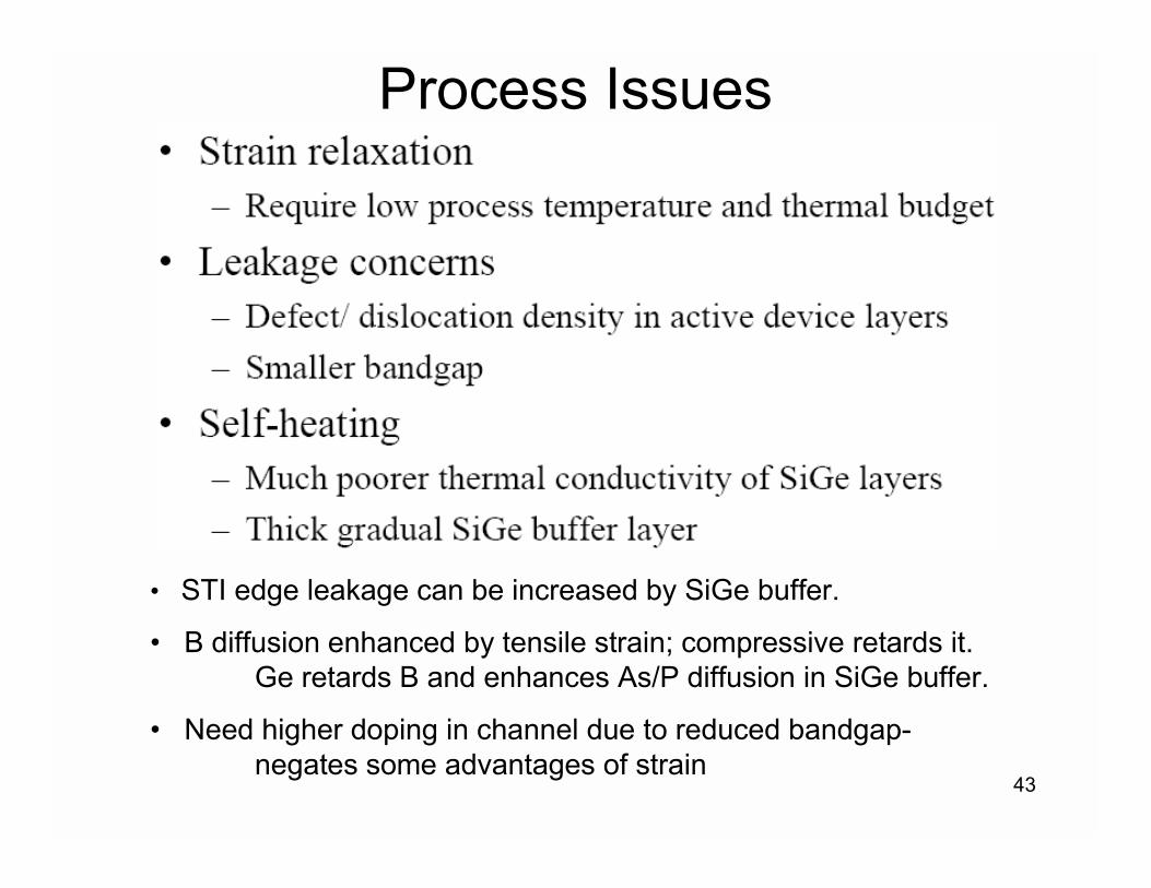
Process Issues
� STI edge leakage can be increased by SiGe buffer.
� B diffusion enhanced by tensile strain; compressive retards it. Ge retards B and enhances As/P diffusion in SiGe buffer.
� Need higher doping in channel due to reduced bandgap-negates some advantages of strain

44
Defects in Strained Si
45
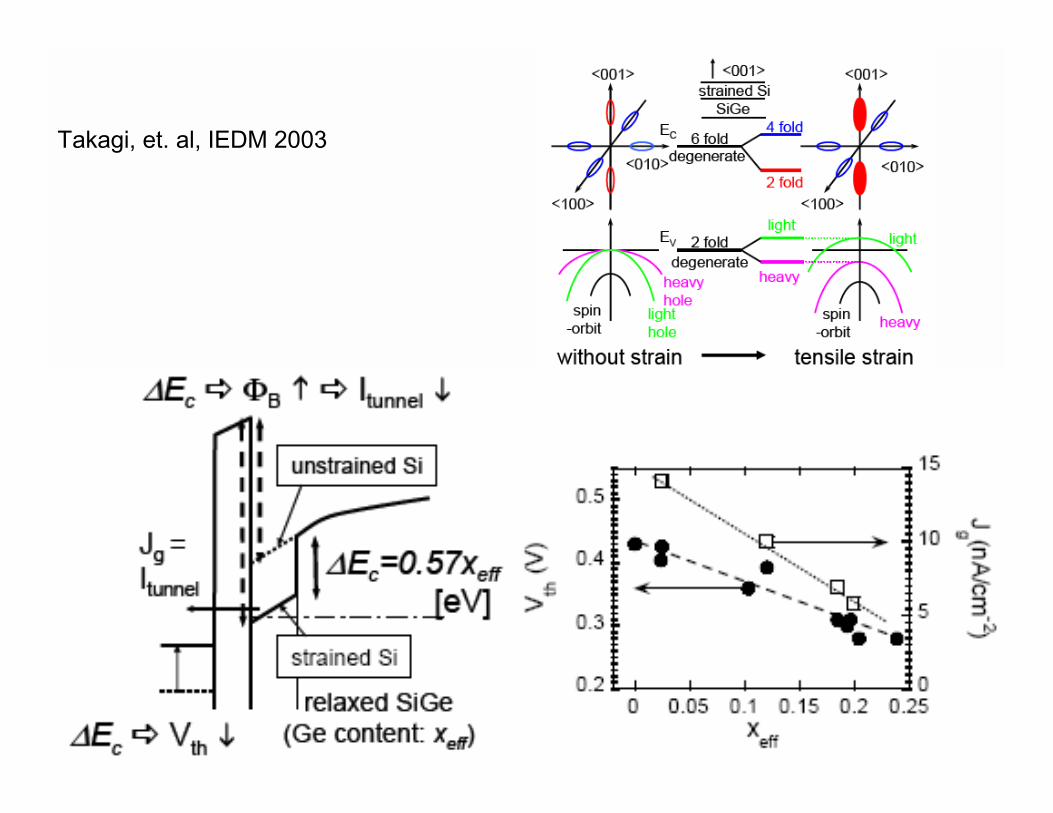
Takagi, et. al, IEDM 2003
46
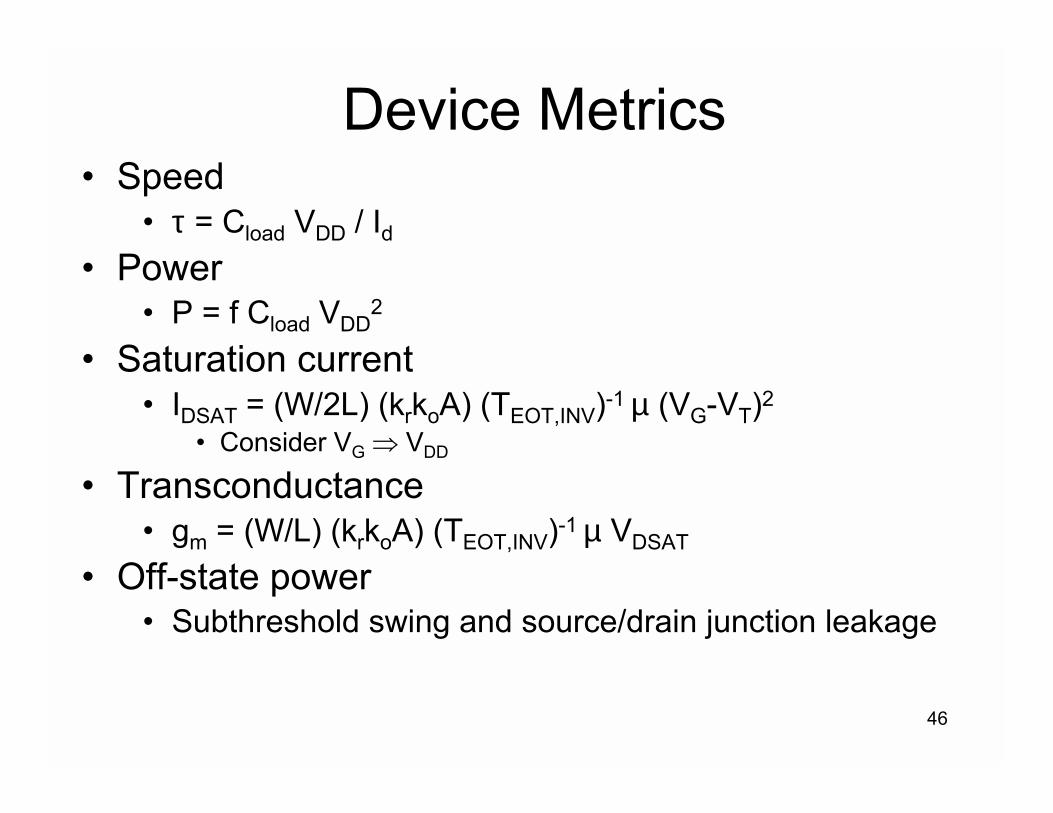
Device Metrics� Speed
� τ = Cload VDD / Id� Power
� P = f Cload VDD2
� Saturation current� IDSAT = (W/2L) (krkoA) (TEOT,INV)-1 µ (VG-VT)2
� Consider VG ⇒ VDD
� Transconductance� gm = (W/L) (krkoA) (TEOT,INV)-1 µ VDSAT
� Off-state power� Subthreshold swing and source/drain junction leakage