Embed Size (px)
Citation preview
A
BY
Product
Folder
Sample &Buy
Technical
Documents
Tools &
Software
Support &Community
SN74AHC1G02SCLS342M –APRIL 1996–REVISED DECEMBER 2014
SN74AHC1G02 Single 2-Input Positive-NOR Gate1 Features 2 Applications1• Operating Range of 2 V to 5.5 V • Infotainment• Max tpd of 6.5 ns at 5 V • Printers• Low Power Consumption, 10-µA Max ICC • Cameras• ±8-mA Output Drive at 5 V • PCs, Notebooks• Schmitt Trigger Action at All Inputs Makes the • E-Meters
Circuit Tolerant for Slower Input Rise and Fall • Body Control ModulesTime
3 Description• ESD Protection Exceeds JESD 22This device contains a single 2-input NOR gate that– 2000-V Human-Body Modelperforms the Boolean function Y = A × B or Y = A + B– 200-V Machine Model in positive logic.
– 1000-V Charged-Device ModelDevice Information(1)
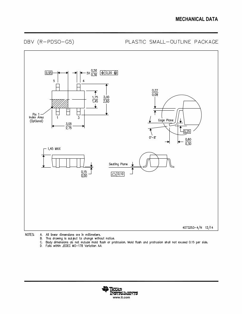
PART NUMBER PACKAGE BODY SIZE (NOM)SOT-23 (5) 2.90 mm x 1.60 mm
SN74AHC1G02 SC-70 (5) 2.00 mm x 1.30 mmSOT-553 (5) 1.65 mm x 1.20 mm
(1) For all available packages, see the orderable addendum atthe end of the data sheet.
4 Simplified Schematic
1
An IMPORTANT NOTICE at the end of this data sheet addresses availability, warranty, changes, use in safety-critical applications,intellectual property matters and other important disclaimers. PRODUCTION DATA.
SN74AHC1G02SCLS342M –APRIL 1996–REVISED DECEMBER 2014 www.ti.com
Table of Contents1 Features .................................................................. 1 9 Detailed Description .............................................. 8
9.1 Overview ................................................................... 82 Applications ........................................................... 19.2 Functional Block Diagram ......................................... 83 Description ............................................................. 19.3 Feature Description................................................... 84 Simplified Schematic............................................. 19.4 Device Functional Modes.......................................... 85 Revision History..................................................... 2
10 Application and Implementation.......................... 96 Pin Configuration and Functions ......................... 310.1 Application Information............................................ 97 Specifications......................................................... 410.2 Typical Application ................................................. 97.1 Absolute Maximum Ratings ..................................... 4
11 Power Supply Recommendations ..................... 107.2 ESD Ratings.............................................................. 412 Layout................................................................... 117.3 Recommended Operating Conditions....................... 4
12.1 Layout Guidelines ................................................. 117.4 Thermal Information .................................................. 512.2 Layout Example .................................................... 117.5 Electrical Characteristics........................................... 5
13 Device and Documentation Support ................. 117.6 Switching Characteristics, VCC = 3.3 V ± 0.3 V ........ 513.1 Trademarks ........................................................... 117.7 Switching Characteristics, VCC = 5 V ± 0.5 V ........... 513.2 Electrostatic Discharge Caution............................ 117.8 Operating Characteristics.......................................... 613.3 Glossary ................................................................ 117.9 Typical Characteristics .............................................. 6
14 Mechanical, Packaging, and Orderable8 Parameter Measurement Information .................. 7Information ........................................................... 11
5 Revision History
Changes from Revision L (June 2005) to Revision M Page
• Added Applications, Device Information table, Pin Functions table, ESD Ratings table, Thermal Information table,Typical Characteristics, Feature Description section, Device Functional Modes, Application and Implementationsection, Power Supply Recommendations section, Layout section, Device and Documentation Support section, andMechanical, Packaging, and Orderable Information section. ................................................................................................. 1
• Deleted Ordering Information table. ....................................................................................................................................... 1• Changed MAX operating temperature in Recommended Operating Conditions table. ......................................................... 4
2 Submit Documentation Feedback Copyright © 1996–2014, Texas Instruments Incorporated
Product Folder Links: SN74AHC1G02
3
2
4
51A VCC
Y
B
GND
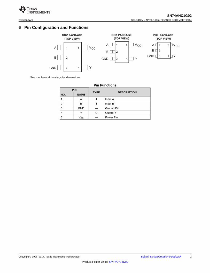
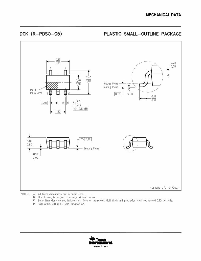
DBV PACKAGE
(TOP VIEW)
DCK PACKAGE
(TOP VIEW)
3
2
4
51A VCC
Y
B
GND
3
2
4
51A VCC
Y
B
GND
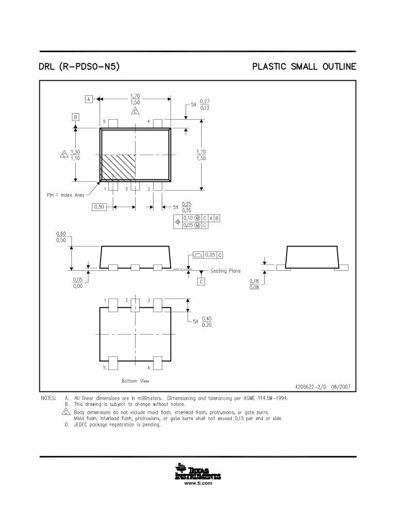
DRL PACKAGE
(TOP VIEW)
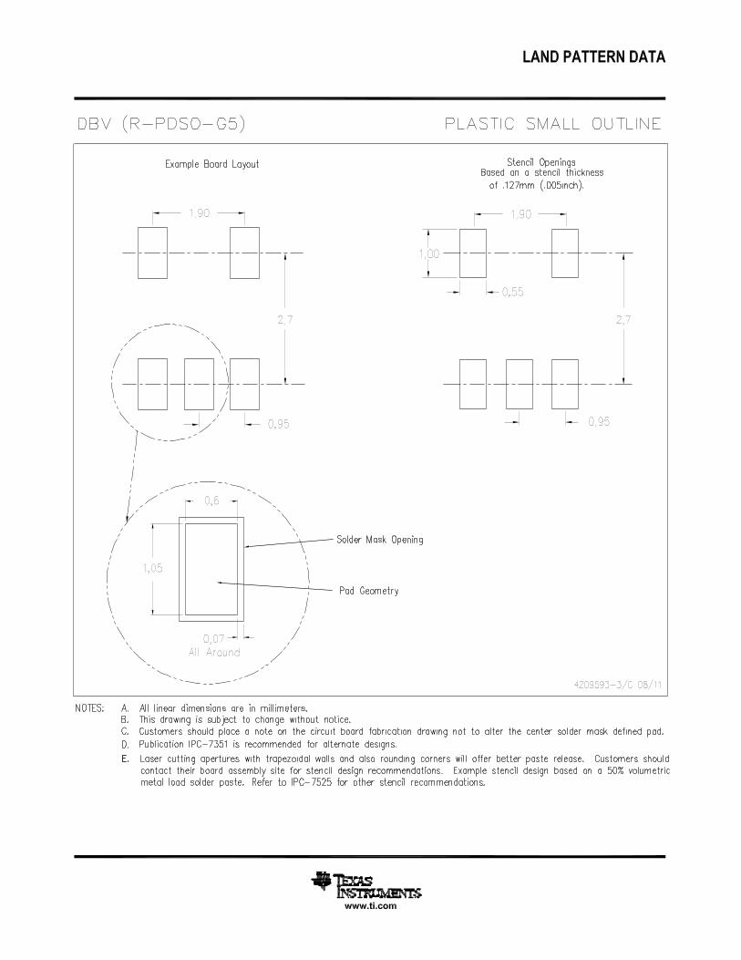
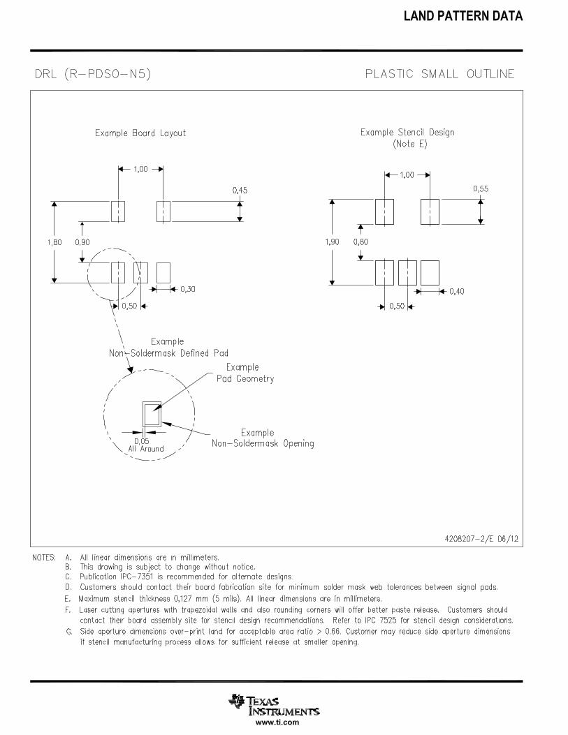
See mechanical drawings for dimensions.
SN74AHC1G02www.ti.com SCLS342M –APRIL 1996–REVISED DECEMBER 2014
6 Pin Configuration and Functions
Pin FunctionsPIN
TYPE DESCRIPTIONNO. NAME1 A I Input A2 B I Input B3 GND — Ground Pin4 Y O Output Y5 VCC — Power Pin
Copyright © 1996–2014, Texas Instruments Incorporated Submit Documentation Feedback 3
Product Folder Links: SN74AHC1G02
SN74AHC1G02SCLS342M –APRIL 1996–REVISED DECEMBER 2014 www.ti.com
7 Specifications
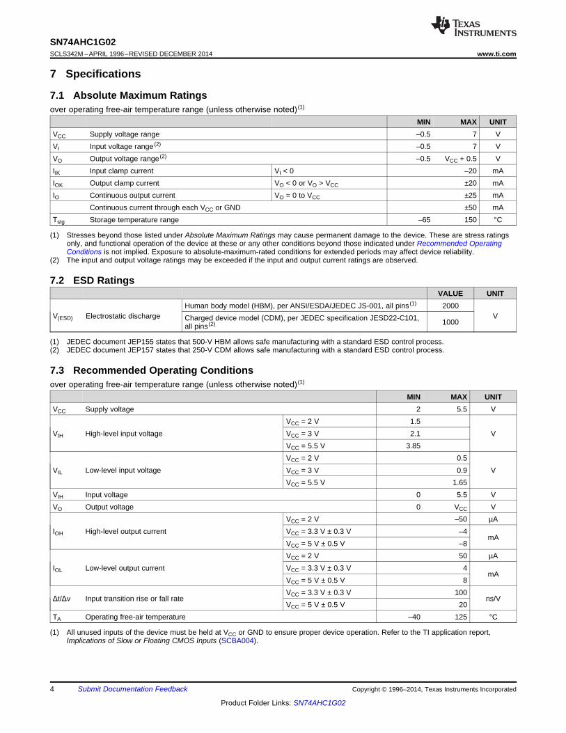
7.1 Absolute Maximum Ratingsover operating free-air temperature range (unless otherwise noted) (1)
MIN MAX UNITVCC Supply voltage range –0.5 7 VVI Input voltage range (2) –0.5 7 VVO Output voltage range (2) –0.5 VCC + 0.5 VIIK Input clamp current VI < 0 –20 mAIOK Output clamp current VO < 0 or VO > VCC ±20 mAIO Continuous output current VO = 0 to VCC ±25 mA
Continuous current through each VCC or GND ±50 mATstg Storage temperature range –65 150 °C
(1) Stresses beyond those listed under Absolute Maximum Ratings may cause permanent damage to the device. These are stress ratingsonly, and functional operation of the device at these or any other conditions beyond those indicated under Recommended OperatingConditions is not implied. Exposure to absolute-maximum-rated conditions for extended periods may affect device reliability.
(2) The input and output voltage ratings may be exceeded if the input and output current ratings are observed.
7.2 ESD RatingsVALUE UNIT
Human body model (HBM), per ANSI/ESDA/JEDEC JS-001, all pins (1) 2000V(ESD) Electrostatic discharge VCharged device model (CDM), per JEDEC specification JESD22-C101, 1000all pins (2)
(1) JEDEC document JEP155 states that 500-V HBM allows safe manufacturing with a standard ESD control process.(2) JEDEC document JEP157 states that 250-V CDM allows safe manufacturing with a standard ESD control process.
7.3 Recommended Operating Conditionsover operating free-air temperature range (unless otherwise noted) (1)
MIN MAX UNITVCC Supply voltage 2 5.5 V
VCC = 2 V 1.5VIH High-level input voltage VCC = 3 V 2.1 V
VCC = 5.5 V 3.85VCC = 2 V 0.5
VIL Low-level input voltage VCC = 3 V 0.9 VVCC = 5.5 V 1.65
VIH Input voltage 0 5.5 VVO Output voltage 0 VCC V
VCC = 2 V –50 µAIOH High-level output current VCC = 3.3 V ± 0.3 V –4
mAVCC = 5 V ± 0.5 V –8VCC = 2 V 50 µA
IOL Low-level output current VCC = 3.3 V ± 0.3 V 4mA
VCC = 5 V ± 0.5 V 8VCC = 3.3 V ± 0.3 V 100
Δt/Δv Input transition rise or fall rate ns/VVCC = 5 V ± 0.5 V 20
TA Operating free-air temperature –40 125 °C
(1) All unused inputs of the device must be held at VCC or GND to ensure proper device operation. Refer to the TI application report,Implications of Slow or Floating CMOS Inputs (SCBA004).
4 Submit Documentation Feedback Copyright © 1996–2014, Texas Instruments Incorporated
Product Folder Links: SN74AHC1G02
SN74AHC1G02www.ti.com SCLS342M –APRIL 1996–REVISED DECEMBER 2014
7.4 Thermal InformationSN74AHC1G02
THERMAL METRIC (1) DBV DCK DRL UNIT5 PINS
RθJA Junction-to-ambient thermal resistance 231.3 287.6 328.7RθJC(top) Junction-to-case (top) thermal resistance 119.9 97.7 105.1RθJB Junction-to-board thermal resistance 60.6 65. 150.3 °C/WψJT Junction-to-top characterization parameter 17.8 2.0 6.9ψJB Junction-to-board characterization parameter 60.1 64.2 148.4
(1) For more information about traditional and new thermal metrics, see the IC Package Thermal Metrics application report (SPRA953).
7.5 Electrical Characteristicsover operating free-air temperature range (unless otherwise noted)
TA = 25°C –40°C to 85°C –40°C to 125°CPARAMETER TEST CONDITIONS VCC UNIT
MIN TYP MAX MIN MAX MIN MAX2 V 1.9 2 1.9 1.9
IOH = –50 µA 3 V 2.9 3 2.9 2.9VOH 4.5 V 4.4 4.5 4.4 4.4 V
IOH = –4 mA 3 V 2.58 2.48 2.48IOH = –8 mA 4.5 V 3.94 3.8 3.8
2 V 0.1 0.1 0.1IOH = 50 µA 3 V 0.1 0.1 0.1
VOL 4.5 V 0.1 0.1 0.1 VIOL = 4 mA 3 V 0.36 0.44 0.44IOL = 8 mA 4.5 V 0.36 0.44 0.44
0 V toII VI = 5.5 V or GND ±0.1 ±1 ±1 µA5.5 VICC VI = VCC or GND, IO = 0 5.5 V 1 10 10 µACi VI = VCC or GND 5 V 4 10 10 10 pF
7.6 Switching Characteristics, VCC = 3.3 V ± 0.3 Vover recommended operating free-air temperature range (unless otherwise noted) (see Figure 3)
TA = 25°C –40°C to 85°C –40°C to 125°CFROM TO OUTPUTPARAMETER UNIT(INPUT) (OUTPUT) CAPACITANCE MIN TYP MAX MIN MAX MIN MAXtPLH 5.6 7.9 1 9.5 1 10.5
A Y CL = 15 pF nstPHL 5.6 7.9 1 9.5 1 10.5tPLH 8.1 11.4 1 13 1 14
A Y CL = 50 pF nstPHL 8.1 11.4 1 13 1 14
7.7 Switching Characteristics, VCC = 5 V ± 0.5 Vover recommended operating free-air temperature range (unless otherwise noted) (see Figure 3)
TA = 25°C –40°C to 85°C –40°C to 125°CFROM TO OUTPUTPARAMETER UNIT(INPUT) (OUTPUT) CAPACITANCE MIN TYP MAX MIN MAX MIN MAXtPLH 3.6 5.5 1 6.5 1 7
A Y CL = 15 pF nstPHL 3.6 5.5 1 6.5 1 7tPLH 5.1 7.5 1 8.5 1 9
A Y CL = 50 pF nstPHL 5.1 7.5 1 8.5 1 9
Copyright © 1996–2014, Texas Instruments Incorporated Submit Documentation Feedback 5
Product Folder Links: SN74AHC1G02
Temperature (qC)
TP
D (
ns)
-100 -50 0 50 100 1500
1
2
3
4
5
D001
TPD in ns
VccY
Axi
s T
itle
(Uni
t)
0 1 2 3 4 5 60
1
2
3
4
5
6
7
D002
TPD in ns
SN74AHC1G02SCLS342M –APRIL 1996–REVISED DECEMBER 2014 www.ti.com
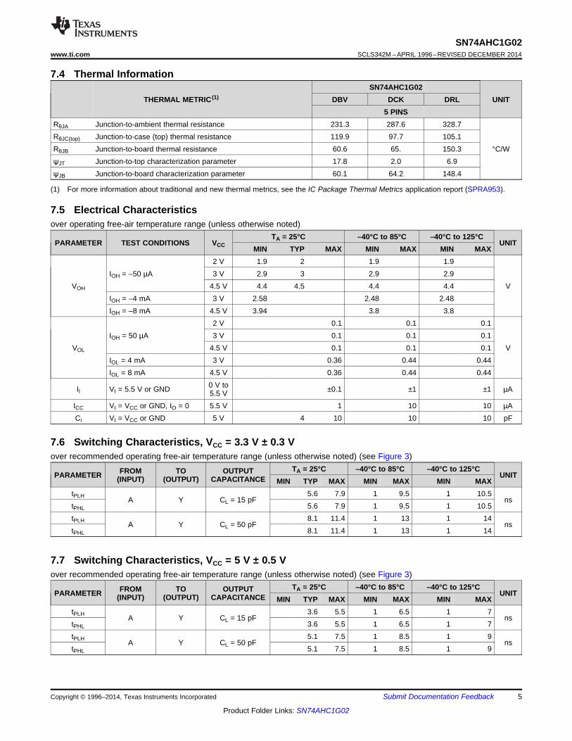
7.8 Operating CharacteristicsVCC = 5 V, TA = 25°C
PARAMETER TEST CONDITIONS TYP UNITCpd Power dissipation capacitance No load, f = 1 MHz 15 pF
7.9 Typical Characteristics
Figure 1. TPD vs Temperature Figure 2. TPD vs VCC at 25°C
6 Submit Documentation Feedback Copyright © 1996–2014, Texas Instruments Incorporated
Product Folder Links: SN74AHC1G02
50% VCC
VCC
VCC
0 V
0 V
thtsu
VOLTAGE WAVEFORMS
SETUP AND HOLD TIMES
Data Input
tPLH
tPHL
tPHL
tPLH
VOH
VOH
VOL
VOL
VCC
0 V
50% VCC50% VCC
Input
Out-of-Phase
Output
In-Phase
Output
Timing Input
50% VCC
VOLTAGE WAVEFORMS
PROPAGATION DELAY TIMES
INVERTING AND NONINVERTING OUTPUTS
Output
Control
Output
Waveform 1
S1 at VCC(see Note B)
Output
Waveform 2
S1 at GND
(see Note B)
VOL
VOH
tPZL
tPZH
tPLZ
tPHZ
≈VCC
0 V
50% VCC VOL + 0.3 V
50% VCC≈0 V
VCC
VOLTAGE WAVEFORMS
ENABLE AND DISABLE TIMES
LOW- AND HIGH-LEVEL ENABLING
tPLH/tPHLtPLZ/tPZLtPHZ/tPZHOpen Drain
Open
VCCGND
VCC
TEST S1
VCC
0 V
50% VCC
tw
VOLTAGE WAVEFORMS
PULSE DURATION
Input
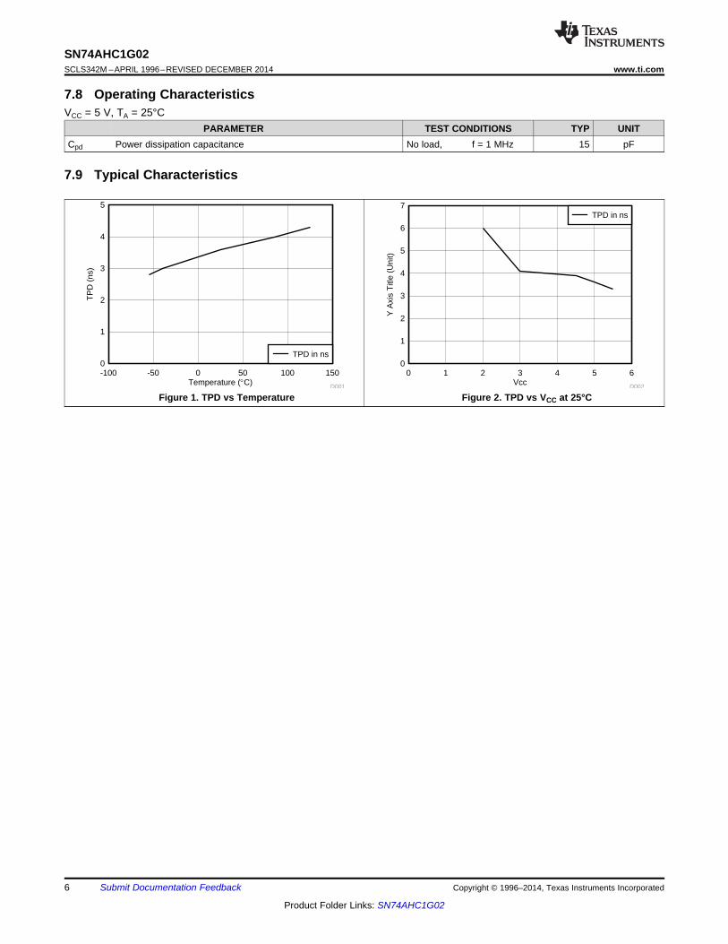
NOTES: A. CL includes probe and jig capacitance.
B. Waveform 1 is for an output with internal conditions such that the output is low, except when disabled by the output control.
Waveform 2 is for an output with internal conditions such that the output is high, except when disabled by the output control.
C. All input pulses are supplied by generators having the following characteristics: PRR ≤ 1 MHz, ZO = 50 Ω, tr ≤ 3 ns, tf ≤ 3 ns.
D. The outputs are measured one at a time, with one input transition per measurement.
E. All parameters and waveforms are not applicable to all devices.
From Output
Under Test
CL(see Note A)
LOAD CIRCUIT FOR
3-STATE AND OPEN-DRAIN OUTPUTS
S1
VCC
RL = 1 kΩ
GNDFrom Output
Under Test
CL(see Note A)
Test
Point
LOAD CIRCUIT FOR
TOTEM-POLE OUTPUTS
Open
50% VCC
50% VCC 50% VCC
50% VCC
50% VCC 50% VCC
50% VCC 50% VCC
VOH − 0.3 V
SN74AHC1G02www.ti.com SCLS342M –APRIL 1996–REVISED DECEMBER 2014
8 Parameter Measurement Information
Figure 3. Load Circuit And Voltage Waveforms
Copyright © 1996–2014, Texas Instruments Incorporated Submit Documentation Feedback 7
Product Folder Links: SN74AHC1G02
A
BY
SN74AHC1G02SCLS342M –APRIL 1996–REVISED DECEMBER 2014 www.ti.com
9 Detailed Description
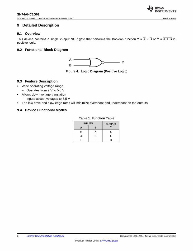
9.1 OverviewThis device contains a single 2-input NOR gate that performs the Boolean function Y = A × B or Y = A + B inpositive logic.
9.2 Functional Block Diagram
Figure 4. Logic Diagram (Positive Logic)
9.3 Feature Description• Wide operating voltage range
– Operates from 2 V to 5.5 V• Allows down-voltage translation
– Inputs accept voltages to 5.5 V• The low drive and slow edge rates will minimize overshoot and undershoot on the outputs
9.4 Device Functional Modes
Table 1. Function TableINPUTS OUTPUT
YA BH X LX H LL L H
8 Submit Documentation Feedback Copyright © 1996–2014, Texas Instruments Incorporated
Product Folder Links: SN74AHC1G02
3.3-V or 5-V regulated
0.1 Fµ
5-V accessory
5-VSystemLogic
µC orSystemLogic
SN74AHC1G02www.ti.com SCLS342M –APRIL 1996–REVISED DECEMBER 2014
10 Application and Implementation
NOTEInformation in the following applications sections is not part of the TI componentspecification, and TI does not warrant its accuracy or completeness. TI’s customers areresponsible for determining suitability of components for their purposes. Customers shouldvalidate and test their design implementation to confirm system functionality.
10.1 Application InformationSN74AHCT1G125 is a low-drive CMOS device that can be used for a multitude of bus interface type applicationswhere output ringing is a concern. The low drive and slow edge rates will minimize overshoot and undershoot onthe outputs. The inputs can accept voltages to 5.5 V at any valid VCC making it Ideal for down translation.
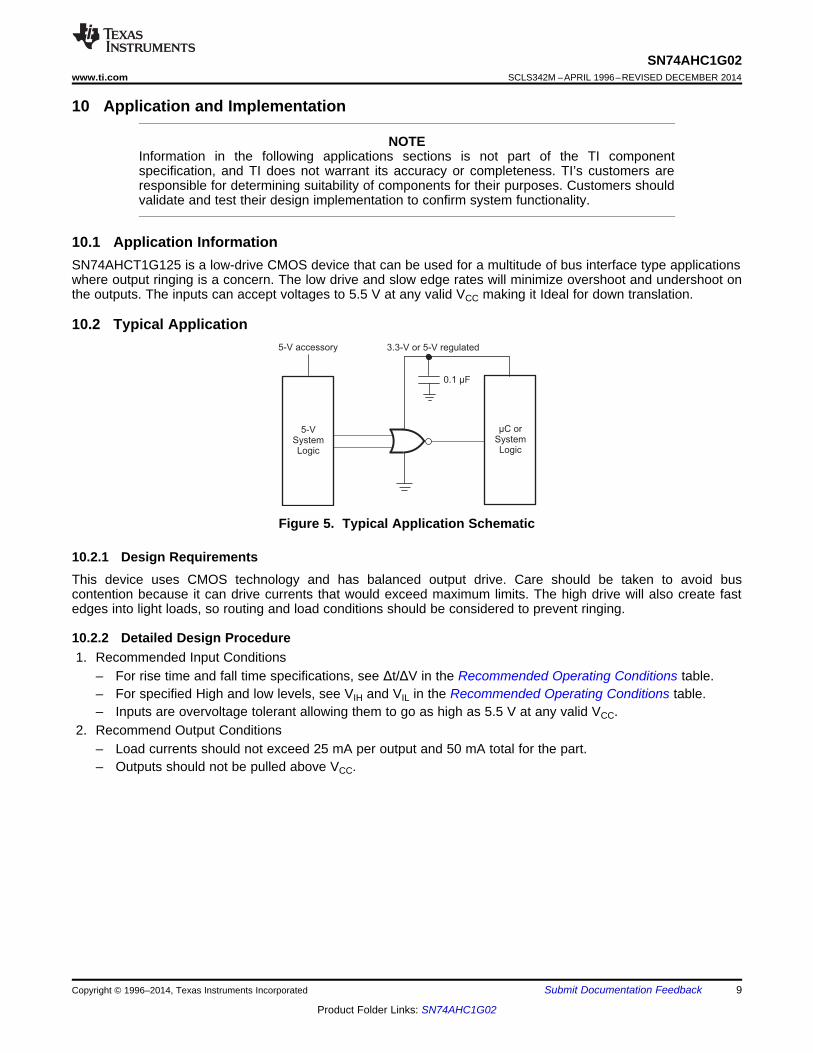
10.2 Typical Application
Figure 5. Typical Application Schematic
10.2.1 Design RequirementsThis device uses CMOS technology and has balanced output drive. Care should be taken to avoid buscontention because it can drive currents that would exceed maximum limits. The high drive will also create fastedges into light loads, so routing and load conditions should be considered to prevent ringing.
10.2.2 Detailed Design Procedure1. Recommended Input Conditions
– For rise time and fall time specifications, see Δt/ΔV in the Recommended Operating Conditions table.– For specified High and low levels, see VIH and VIL in the Recommended Operating Conditions table.– Inputs are overvoltage tolerant allowing them to go as high as 5.5 V at any valid VCC.
2. Recommend Output Conditions– Load currents should not exceed 25 mA per output and 50 mA total for the part.– Outputs should not be pulled above VCC.
Copyright © 1996–2014, Texas Instruments Incorporated Submit Documentation Feedback 9
Product Folder Links: SN74AHC1G02
SN74AHC1G02SCLS342M –APRIL 1996–REVISED DECEMBER 2014 www.ti.com
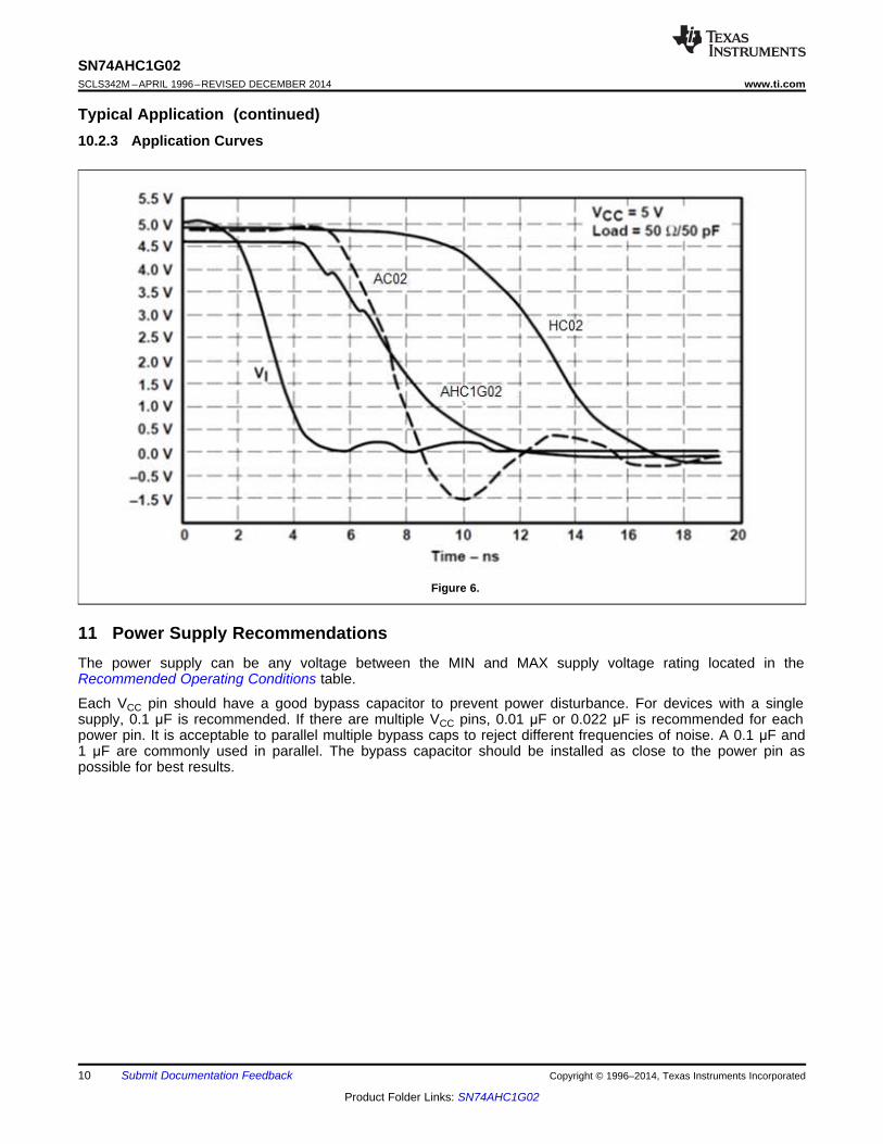
Typical Application (continued)10.2.3 Application Curves
Figure 6.
11 Power Supply RecommendationsThe power supply can be any voltage between the MIN and MAX supply voltage rating located in theRecommended Operating Conditions table.
Each VCC pin should have a good bypass capacitor to prevent power disturbance. For devices with a singlesupply, 0.1 μF is recommended. If there are multiple VCC pins, 0.01 μF or 0.022 μF is recommended for eachpower pin. It is acceptable to parallel multiple bypass caps to reject different frequencies of noise. A 0.1 μF and1 μF are commonly used in parallel. The bypass capacitor should be installed as close to the power pin aspossible for best results.
10 Submit Documentation Feedback Copyright © 1996–2014, Texas Instruments Incorporated
Product Folder Links: SN74AHC1G02
Vcc
Unused Input
Input
Output
Input
Unused Input Output
SN74AHC1G02www.ti.com SCLS342M –APRIL 1996–REVISED DECEMBER 2014
12 Layout
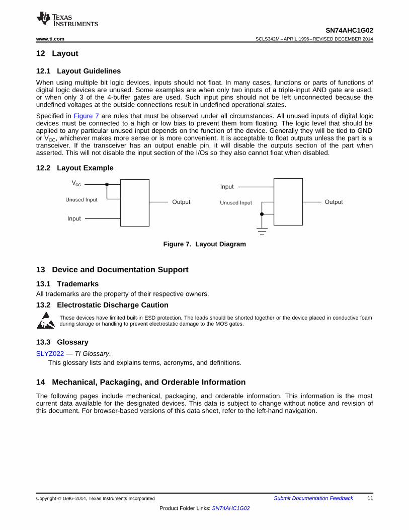
12.1 Layout GuidelinesWhen using multiple bit logic devices, inputs should not float. In many cases, functions or parts of functions ofdigital logic devices are unused. Some examples are when only two inputs of a triple-input AND gate are used,or when only 3 of the 4-buffer gates are used. Such input pins should not be left unconnected because theundefined voltages at the outside connections result in undefined operational states.
Specified in Figure 7 are rules that must be observed under all circumstances. All unused inputs of digital logicdevices must be connected to a high or low bias to prevent them from floating. The logic level that should beapplied to any particular unused input depends on the function of the device. Generally they will be tied to GNDor VCC, whichever makes more sense or is more convenient. It is acceptable to float outputs unless the part is atransceiver. If the transceiver has an output enable pin, it will disable the outputs section of the part whenasserted. This will not disable the input section of the I/Os so they also cannot float when disabled.
12.2 Layout Example
Figure 7. Layout Diagram
13 Device and Documentation Support
13.1 TrademarksAll trademarks are the property of their respective owners.
13.2 Electrostatic Discharge CautionThese devices have limited built-in ESD protection. The leads should be shorted together or the device placed in conductive foamduring storage or handling to prevent electrostatic damage to the MOS gates.
13.3 GlossarySLYZ022 — TI Glossary.
This glossary lists and explains terms, acronyms, and definitions.
14 Mechanical, Packaging, and Orderable InformationThe following pages include mechanical, packaging, and orderable information. This information is the mostcurrent data available for the designated devices. This data is subject to change without notice and revision ofthis document. For browser-based versions of this data sheet, refer to the left-hand navigation.
Copyright © 1996–2014, Texas Instruments Incorporated Submit Documentation Feedback 11
Product Folder Links: SN74AHC1G02
PACKAGE OPTION ADDENDUM
www.ti.com 3-Sep-2015
Addendum-Page 1
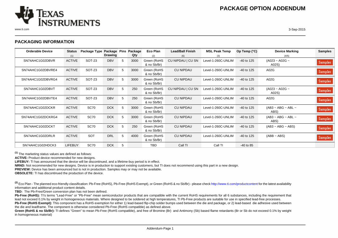
PACKAGING INFORMATION
Orderable Device Status(1)
Package Type PackageDrawing
Pins PackageQty
Eco Plan(2)
Lead/Ball Finish(6)
MSL Peak Temp(3)
Op Temp (°C) Device Marking(4/5)
Samples
SN74AHC1G02DBVR ACTIVE SOT-23 DBV 5 3000 Green (RoHS& no Sb/Br)
CU NIPDAU | CU SN Level-1-260C-UNLIM -40 to 125 (A023 ~ A02G ~ A02S)
SN74AHC1G02DBVRE4 ACTIVE SOT-23 DBV 5 3000 Green (RoHS& no Sb/Br)
CU NIPDAU Level-1-260C-UNLIM -40 to 125 A02G
SN74AHC1G02DBVRG4 ACTIVE SOT-23 DBV 5 3000 Green (RoHS& no Sb/Br)
CU NIPDAU Level-1-260C-UNLIM -40 to 125 A02G
SN74AHC1G02DBVT ACTIVE SOT-23 DBV 5 250 Green (RoHS& no Sb/Br)
CU NIPDAU | CU SN Level-1-260C-UNLIM -40 to 125 (A023 ~ A02G ~ A02S)
SN74AHC1G02DBVTE4 ACTIVE SOT-23 DBV 5 250 Green (RoHS& no Sb/Br)
CU NIPDAU Level-1-260C-UNLIM -40 to 125 A02G
SN74AHC1G02DCKR ACTIVE SC70 DCK 5 3000 Green (RoHS& no Sb/Br)
CU NIPDAU Level-1-260C-UNLIM -40 to 125 (AB3 ~ ABG ~ ABL ~ ABS)
SN74AHC1G02DCKRG4 ACTIVE SC70 DCK 5 3000 Green (RoHS& no Sb/Br)
CU NIPDAU Level-1-260C-UNLIM -40 to 125 (AB3 ~ ABG ~ ABL ~ ABS)
SN74AHC1G02DCKT ACTIVE SC70 DCK 5 250 Green (RoHS& no Sb/Br)
CU NIPDAU Level-1-260C-UNLIM -40 to 125 (AB3 ~ ABG ~ ABS)
SN74AHC1G02DRLR ACTIVE SOT DRL 5 4000 Green (RoHS& no Sb/Br)
CU NIPDAU Level-1-260C-UNLIM -40 to 125 (ABB ~ ABS)
SN74AHC1G02HDCK3 LIFEBUY SC70 DCK 5 TBD Call TI Call TI -40 to 85 (1) The marketing status values are defined as follows:ACTIVE: Product device recommended for new designs.LIFEBUY: TI has announced that the device will be discontinued, and a lifetime-buy period is in effect.NRND: Not recommended for new designs. Device is in production to support existing customers, but TI does not recommend using this part in a new design.PREVIEW: Device has been announced but is not in production. Samples may or may not be available.OBSOLETE: TI has discontinued the production of the device.
(2) Eco Plan - The planned eco-friendly classification: Pb-Free (RoHS), Pb-Free (RoHS Exempt), or Green (RoHS & no Sb/Br) - please check http://www.ti.com/productcontent for the latest availabilityinformation and additional product content details.TBD: The Pb-Free/Green conversion plan has not been defined.Pb-Free (RoHS): TI's terms "Lead-Free" or "Pb-Free" mean semiconductor products that are compatible with the current RoHS requirements for all 6 substances, including the requirement thatlead not exceed 0.1% by weight in homogeneous materials. Where designed to be soldered at high temperatures, TI Pb-Free products are suitable for use in specified lead-free processes.Pb-Free (RoHS Exempt): This component has a RoHS exemption for either 1) lead-based flip-chip solder bumps used between the die and package, or 2) lead-based die adhesive used betweenthe die and leadframe. The component is otherwise considered Pb-Free (RoHS compatible) as defined above.Green (RoHS & no Sb/Br): TI defines "Green" to mean Pb-Free (RoHS compatible), and free of Bromine (Br) and Antimony (Sb) based flame retardants (Br or Sb do not exceed 0.1% by weightin homogeneous material)
PACKAGE OPTION ADDENDUM
www.ti.com 3-Sep-2015
Addendum-Page 2
(3) MSL, Peak Temp. - The Moisture Sensitivity Level rating according to the JEDEC industry standard classifications, and peak solder temperature.
(4) There may be additional marking, which relates to the logo, the lot trace code information, or the environmental category on the device.
(5) Multiple Device Markings will be inside parentheses. Only one Device Marking contained in parentheses and separated by a "~" will appear on a device. If a line is indented then it is a continuationof the previous line and the two combined represent the entire Device Marking for that device.
(6) Lead/Ball Finish - Orderable Devices may have multiple material finish options. Finish options are separated by a vertical ruled line. Lead/Ball Finish values may wrap to two lines if the finishvalue exceeds the maximum column width.
Important Information and Disclaimer:The information provided on this page represents TI's knowledge and belief as of the date that it is provided. TI bases its knowledge and belief on informationprovided by third parties, and makes no representation or warranty as to the accuracy of such information. Efforts are underway to better integrate information from third parties. TI has taken andcontinues to take reasonable steps to provide representative and accurate information but may not have conducted destructive testing or chemical analysis on incoming materials and chemicals.TI and TI suppliers consider certain information to be proprietary, and thus CAS numbers and other limited information may not be available for release.
In no event shall TI's liability arising out of such information exceed the total purchase price of the TI part(s) at issue in this document sold by TI to Customer on an annual basis.
OTHER QUALIFIED VERSIONS OF SN74AHC1G02 :
• Enhanced Product: SN74AHC1G02-EP
NOTE: Qualified Version Definitions:
• Enhanced Product - Supports Defense, Aerospace and Medical Applications
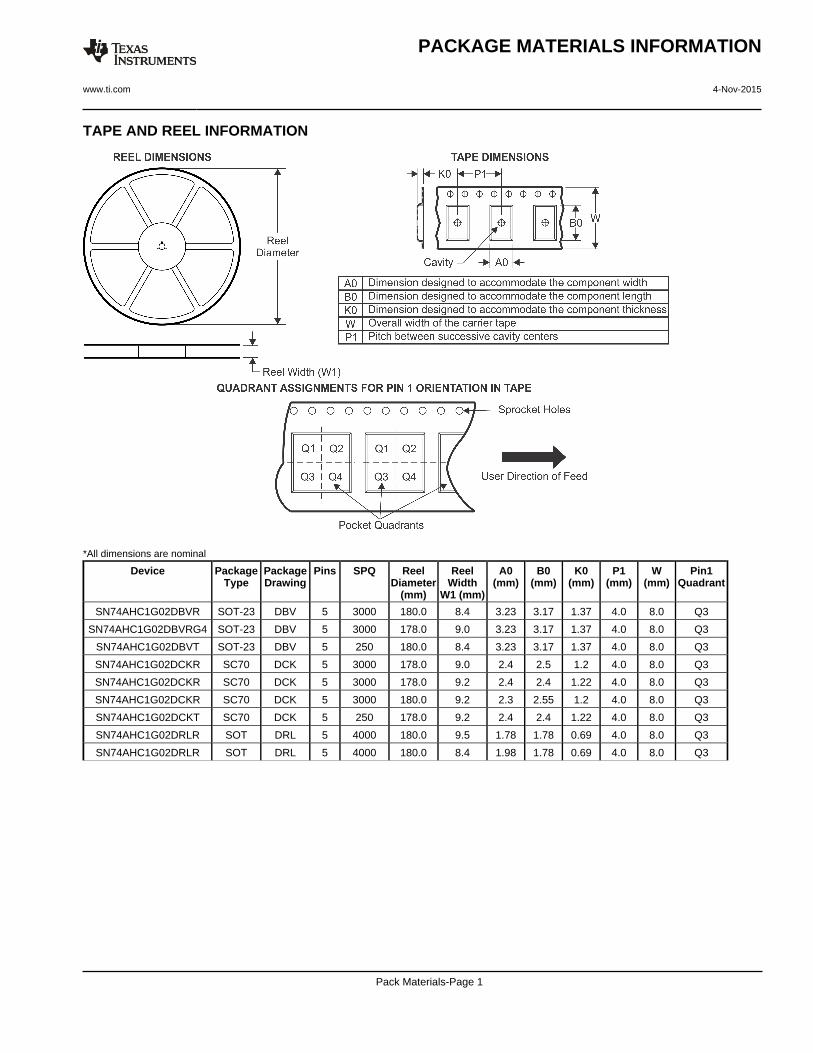
TAPE AND REEL INFORMATION
*All dimensions are nominal
Device PackageType
PackageDrawing
Pins SPQ ReelDiameter
(mm)
ReelWidth
W1 (mm)
A0(mm)
B0(mm)
K0(mm)
P1(mm)
W(mm)
Pin1Quadrant
SN74AHC1G02DBVR SOT-23 DBV 5 3000 180.0 8.4 3.23 3.17 1.37 4.0 8.0 Q3
SN74AHC1G02DBVRG4 SOT-23 DBV 5 3000 178.0 9.0 3.23 3.17 1.37 4.0 8.0 Q3
SN74AHC1G02DBVT SOT-23 DBV 5 250 180.0 8.4 3.23 3.17 1.37 4.0 8.0 Q3
SN74AHC1G02DCKR SC70 DCK 5 3000 178.0 9.0 2.4 2.5 1.2 4.0 8.0 Q3
SN74AHC1G02DCKR SC70 DCK 5 3000 178.0 9.2 2.4 2.4 1.22 4.0 8.0 Q3
SN74AHC1G02DCKR SC70 DCK 5 3000 180.0 9.2 2.3 2.55 1.2 4.0 8.0 Q3
SN74AHC1G02DCKT SC70 DCK 5 250 178.0 9.2 2.4 2.4 1.22 4.0 8.0 Q3
SN74AHC1G02DRLR SOT DRL 5 4000 180.0 9.5 1.78 1.78 0.69 4.0 8.0 Q3
SN74AHC1G02DRLR SOT DRL 5 4000 180.0 8.4 1.98 1.78 0.69 4.0 8.0 Q3
PACKAGE MATERIALS INFORMATION
www.ti.com 4-Nov-2015
Pack Materials-Page 1
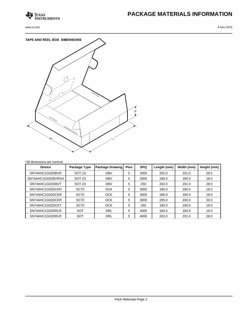
*All dimensions are nominal
Device Package Type Package Drawing Pins SPQ Length (mm) Width (mm) Height (mm)
SN74AHC1G02DBVR SOT-23 DBV 5 3000 202.0 201.0 28.0
SN74AHC1G02DBVRG4 SOT-23 DBV 5 3000 180.0 180.0 18.0
SN74AHC1G02DBVT SOT-23 DBV 5 250 202.0 201.0 28.0
SN74AHC1G02DCKR SC70 DCK 5 3000 180.0 180.0 18.0
SN74AHC1G02DCKR SC70 DCK 5 3000 180.0 180.0 18.0
SN74AHC1G02DCKR SC70 DCK 5 3000 205.0 200.0 33.0
SN74AHC1G02DCKT SC70 DCK 5 250 180.0 180.0 18.0
SN74AHC1G02DRLR SOT DRL 5 4000 184.0 184.0 19.0
SN74AHC1G02DRLR SOT DRL 5 4000 202.0 201.0 28.0
PACKAGE MATERIALS INFORMATION
www.ti.com 4-Nov-2015
Pack Materials-Page 2
IMPORTANT NOTICE
Texas Instruments Incorporated and its subsidiaries (TI) reserve the right to make corrections, enhancements, improvements and otherchanges to its semiconductor products and services per JESD46, latest issue, and to discontinue any product or service per JESD48, latestissue. Buyers should obtain the latest relevant information before placing orders and should verify that such information is current andcomplete. All semiconductor products (also referred to herein as “components”) are sold subject to TI’s terms and conditions of salesupplied at the time of order acknowledgment.TI warrants performance of its components to the specifications applicable at the time of sale, in accordance with the warranty in TI’s termsand conditions of sale of semiconductor products. Testing and other quality control techniques are used to the extent TI deems necessaryto support this warranty. Except where mandated by applicable law, testing of all parameters of each component is not necessarilyperformed.TI assumes no liability for applications assistance or the design of Buyers’ products. Buyers are responsible for their products andapplications using TI components. To minimize the risks associated with Buyers’ products and applications, Buyers should provideadequate design and operating safeguards.TI does not warrant or represent that any license, either express or implied, is granted under any patent right, copyright, mask work right, orother intellectual property right relating to any combination, machine, or process in which TI components or services are used. Informationpublished by TI regarding third-party products or services does not constitute a license to use such products or services or a warranty orendorsement thereof. Use of such information may require a license from a third party under the patents or other intellectual property of thethird party, or a license from TI under the patents or other intellectual property of TI.Reproduction of significant portions of TI information in TI data books or data sheets is permissible only if reproduction is without alterationand is accompanied by all associated warranties, conditions, limitations, and notices. TI is not responsible or liable for such altereddocumentation. Information of third parties may be subject to additional restrictions.Resale of TI components or services with statements different from or beyond the parameters stated by TI for that component or servicevoids all express and any implied warranties for the associated TI component or service and is an unfair and deceptive business practice.TI is not responsible or liable for any such statements.Buyer acknowledges and agrees that it is solely responsible for compliance with all legal, regulatory and safety-related requirementsconcerning its products, and any use of TI components in its applications, notwithstanding any applications-related information or supportthat may be provided by TI. Buyer represents and agrees that it has all the necessary expertise to create and implement safeguards whichanticipate dangerous consequences of failures, monitor failures and their consequences, lessen the likelihood of failures that might causeharm and take appropriate remedial actions. Buyer will fully indemnify TI and its representatives against any damages arising out of the useof any TI components in safety-critical applications.In some cases, TI components may be promoted specifically to facilitate safety-related applications. With such components, TI’s goal is tohelp enable customers to design and create their own end-product solutions that meet applicable functional safety standards andrequirements. Nonetheless, such components are subject to these terms.No TI components are authorized for use in FDA Class III (or similar life-critical medical equipment) unless authorized officers of the partieshave executed a special agreement specifically governing such use.Only those TI components which TI has specifically designated as military grade or “enhanced plastic” are designed and intended for use inmilitary/aerospace applications or environments. Buyer acknowledges and agrees that any military or aerospace use of TI componentswhich have not been so designated is solely at the Buyer's risk, and that Buyer is solely responsible for compliance with all legal andregulatory requirements in connection with such use.TI has specifically designated certain components as meeting ISO/TS16949 requirements, mainly for automotive use. In any case of use ofnon-designated products, TI will not be responsible for any failure to meet ISO/TS16949.
Products ApplicationsAudio www.ti.com/audio Automotive and Transportation www.ti.com/automotiveAmplifiers amplifier.ti.com Communications and Telecom www.ti.com/communicationsData Converters dataconverter.ti.com Computers and Peripherals www.ti.com/computersDLP® Products www.dlp.com Consumer Electronics www.ti.com/consumer-appsDSP dsp.ti.com Energy and Lighting www.ti.com/energyClocks and Timers www.ti.com/clocks Industrial www.ti.com/industrialInterface interface.ti.com Medical www.ti.com/medicalLogic logic.ti.com Security www.ti.com/securityPower Mgmt power.ti.com Space, Avionics and Defense www.ti.com/space-avionics-defenseMicrocontrollers microcontroller.ti.com Video and Imaging www.ti.com/videoRFID www.ti-rfid.comOMAP Applications Processors www.ti.com/omap TI E2E Community e2e.ti.comWireless Connectivity www.ti.com/wirelessconnectivity
Mailing Address: Texas Instruments, Post Office Box 655303, Dallas, Texas 75265Copyright © 2015, Texas Instruments Incorporated


![제04장.ppt [호환 모드] - cms3.koreatech.ac.kr · 제4장 8XNOR8. XNOR 게이트(Exclusive-NORgate)NOR gate) XNOR게이트의기본개념(2입력) 입력중짝수개의1이입력될때출력이1이되고,그렇지않은경우에는](https://img.pdfslide.tips/doc/110x75/5e18f99e86c190143d70c1ae/oe04ppt-eeoe-cms3-oe4-8xnor8-xnor-eoeexclusive-norgatenor.jpg)