Embed Size (px)
Citation preview
The Application and Calculation of Bond Orbital Model on Quantum Semiconductor
鍵結軌道理論在量子半導體之應用與計算

Introduction

Why is the choosing the BOM? a hybrid or link between the k.p and the tight-binding methods combining the virtues of the two above approaches
--the computational effort is comparable to the k.p method
--avoiding the tedious fitting procedure like the tight-binding method
--it is adequate for ultra-thin superlattice
--the boundary condition between materials is treated in the straight-forward manner
--its flexibility to accommodate otherwise awkward geometries
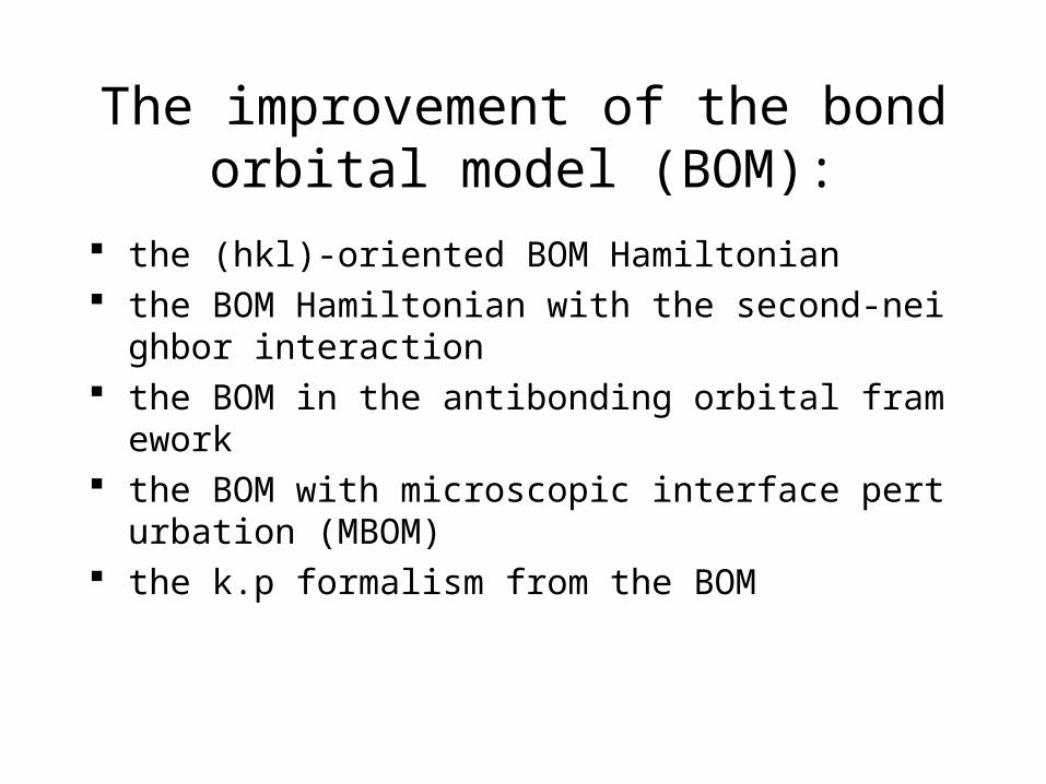
The improvement of the bond orbital model (BOM):
the (hkl)-oriented BOM Hamiltonian the BOM Hamiltonian with the second-neighbor interactio
n the BOM in the antibonding orbital framework the BOM with microscopic interface perturbation (MBO
M) the k.p formalism from the BOM
Bond Orbital Model
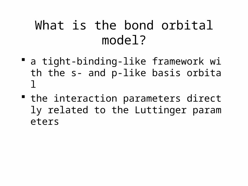
What is the bond orbital model?
a tight-binding-like framework with the s- and p-like basis orbital
the interaction parameters directly related to the Luttinger parameters
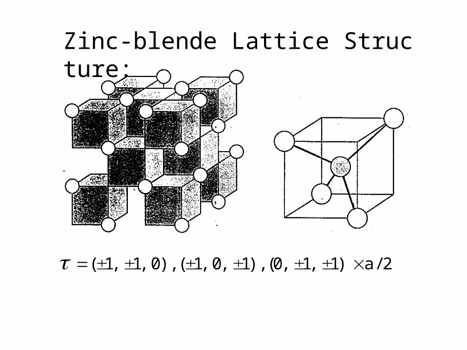
Zinc-blende Lattice Structure:
2/a)1,1,0(),1,0,1(),0,1,1(
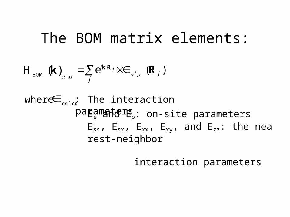
The BOM matrix elements:
,BOM ')(H k )(e,' j
i
j
j RRk
where : The interaction parameters ,'
Es and Ep: on-site parametersEss, Esx, Exx, Exy, and Ezz: the nearest-neighbor interaction parameters
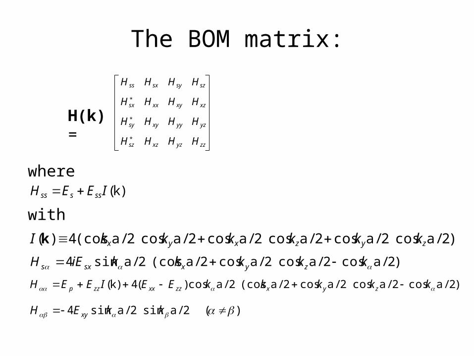
The BOM matrix:
where)k(IEEH sssss
),2/acos2/acos2/acos2/acos2/acos2/a(cos4)( zyzxyx kkkkkkI k
),2/acos2/acos2/acos2/a(cos2/asin4 kkkkkiEH zyxsxs
),2/acos2/acos2/acos2/a(cos2/acos)(4)k( kkkkkEEIEEH zyxzzxxzzp
)(2/asin2/asin4 kkEH xy
with
ssH sxH syH szH
*sxH xxH
xyH
xzH
*syH
xyH
yyH yzH
*szH xzH yzH zzH
H(k)=
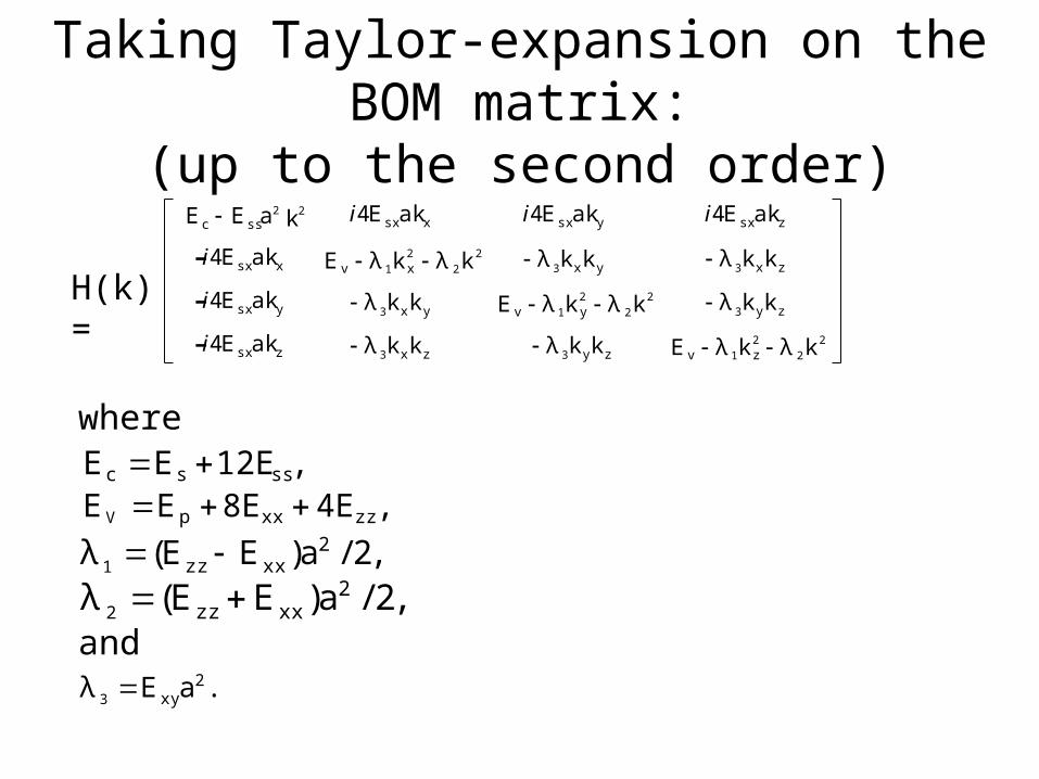
Taking Taylor-expansion on the BOM matrix:
(up to the second order)
where,12EEE sssc
,4E8EEE zzxxpV ,2/a)EE(λ 2
xxzz1 ,2/a)EE(λ 2
xxzz2
.aEλ 2xy3
and
H(k)=
kaEE 22ssc zsx akE4ixsx akE4i
2
2
2
1 kλkλE xv yxkkλ 3
zxkkλ 3
ysx akE4i
yxkkλ 3 2
2
2
1 kλkλE yv zykkλ 3
zxkkλ 3
zykkλ 3 2
2
2
1 kλkλE zv
xsx akE4i-ysx akE4i-zsx akE4i-
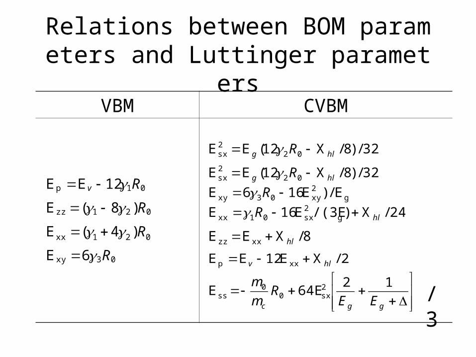
Relations between BOM parameters and Luttinger parameters
VBM CVBM
32/)8/X12(EE 022sx hlg R
32/)8/X12(EE 022sx hlg R
g2xy03xy E/)E166E R
24/X)/(3EE16E g2sx01xx hlR
8/XEE xxzz hl
2/XE12EE xxp hlv
ggc EER
m
m 1264EE 2
sx00
ss /3
03xy 6E R021xx )4(E R 021zz )8(E R
01p 12EE Rv
Bulk Bandstructure:(001)-orientation
Superlattice Bandstructure:(001)-orientation
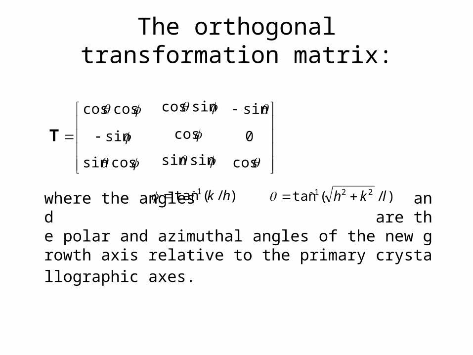
The orthogonal transformation matrix:
cossin
sin
coscos
T
sinsin
cos
sincos
cos
0
sin
where the angles and are the polar and azimuthal angles of the new growth axis relative to the primary crystallographic axes.
)/(tan 221 lkh )/(tan 1 hk
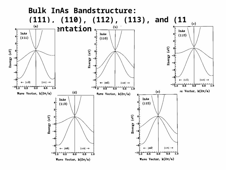
Bulk InAs Bandstructure:(111), (110), (112), (113), and (115)-orientation
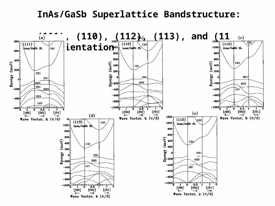
InAs/GaSb Superlattice Bandstructure:(111), (110), (112), (113), and (115)-orientation
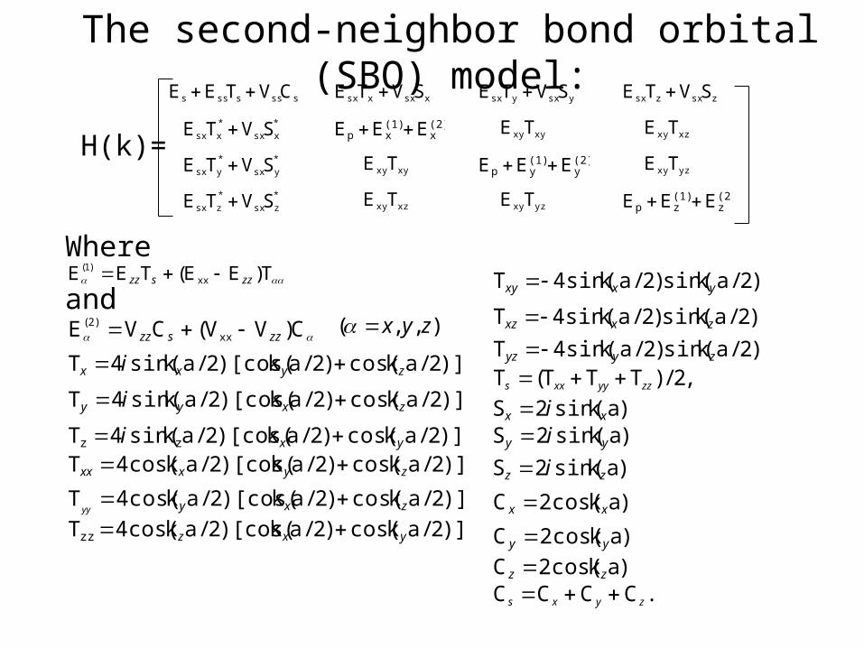
The second-neighbor bond orbital (SBO) model:
Where
and T)EE(TEE xx
)1(
zzszz
),,( zyx C)VV(CVE xx
)2(
zzszz
)],2/akcos()2/ak)[cos(2/aksin(4T zyxx i
)],2/akcos()2/ak)[cos(2/aksin(4T zxyy i
)],2/akcos()2/ak)[cos(2/aksin(4T zz yxi )],2/akcos()2/ak)[cos(2/akcos(4T zyxxx
)],2/akcos()2/ak)[cos(2/akcos(4T zxyyy
)],2/akcos()2/ak)[cos(2/akcos(4Tzz yxz
),2/aksin()2/aksin(4T yxxy
),2/aksin()2/aksin(4T zxxz ),2/aksin()2/aksin(4T zyyz
,2/)TTT(T zzyyxxs ),aksin(2S xx i),aksin(2S yy i),aksin(2S zz i
),akcos(2C xx
),akcos(2C yy ),akcos(2C zz
.CCCC zyxs
sssssss CVTEE xsxxsx SVTE ysxysx SVTE zsxzsx SVTE *
xsx
*
xsx SVTE (2)x
(1)xp EEE xyxyTE
xzxyTE
*
ysx
*
ysx SVTE xyxyTE (2)y
(1)yp EEE
yzxyTE*
zsx
*
zsx SVTE
xzxyTE
yzxyTE
(2)z
(1)zp EEE
H(k)=
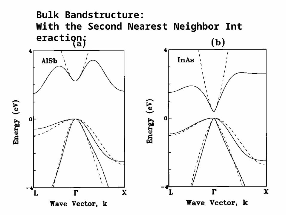
Bulk Bandstructure:With the Second Nearest Neighbor Interaction:
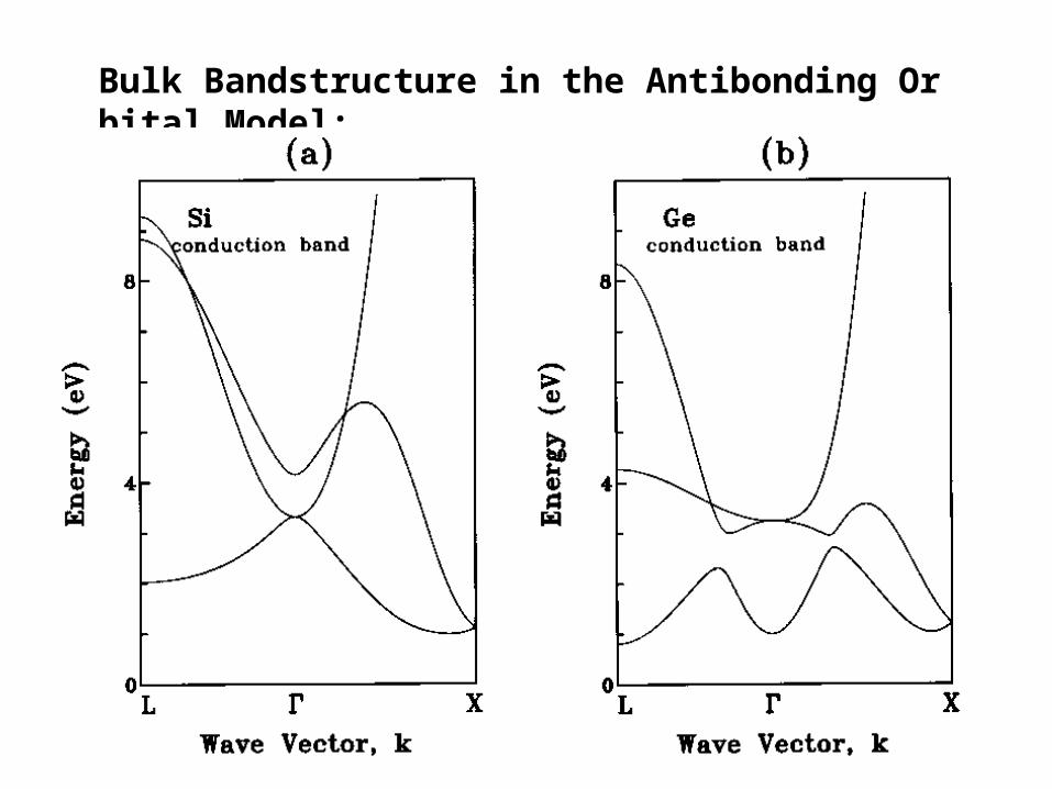
Bulk Bandstructure in the Antibonding Orbital Model:
Bond Orbital Model with MicroscopicEffects
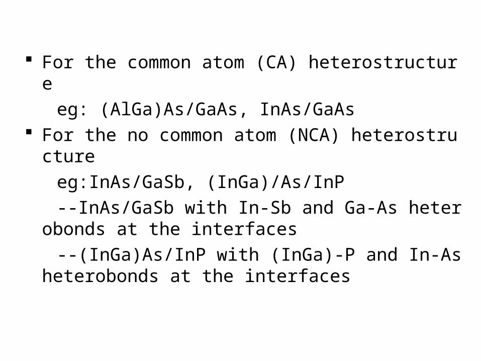
For the common atom (CA) heterostructure
eg: (AlGa)As/GaAs, InAs/GaAs For the no common atom (NCA) heterostructure
eg:InAs/GaSb, (InGa)/As/InP
--InAs/GaSb with In-Sb and Ga-As heterobonds at the interfaces
--(InGa)As/InP with (InGa)-P and In-As heterobonds at the interfaces
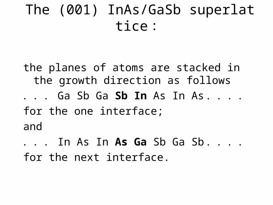
The (001) InAs/GaSb superlattice:
the planes of atoms are stacked in the growth direction as follows
... Ga Sb Ga Sb In As In As....for the one interface;
and
... In As In As Ga Sb Ga Sb....for the next interface.
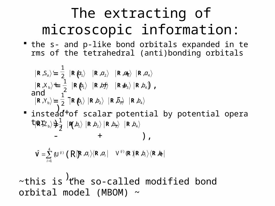
The extracting of microscopic information:
the s- and p-like bond orbitals expanded in terms of the tetrahedral (anti)bonding orbitals
and
instead of scalar potential by potential operator
~this is the so-called modified bond orbital model (MBOM) ~
', aSR = ( + + + ),
1,aR 2,aR 3,aR 4,aR2
1
= ( + - - ),', bXR2
11,bR 2,bR 3,bR 4,bR
= ( - + - ),', bYR 2
11,bR 2,bR 3,bR 4,bR
= ( - - + ),', bZR2
11,bR 2,bR 3,bR 4,bR
(R) + ),
4
1
)((ˆi
iUV ia,R ia,R )()( RiV ib,R ib,R
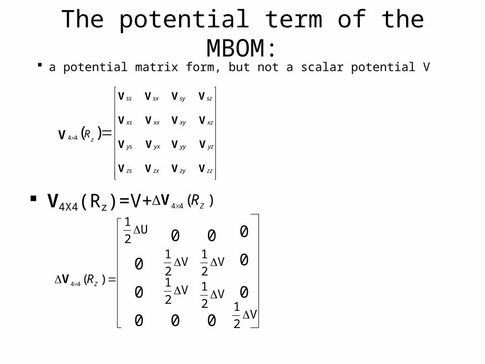
The potential term of the MBOM: a potential matrix form, but not a scalar potential V
VV
VV
VV
VV
V
zxzs
yxys
xxxs
sxss
zR )(44
VV
VV
VV
VV
zzzy
yzyy
xzxy
szsy
V4X4(Rz)=V+ )(44 ZRV
U2
1
0
0
0
)(44 ZRV
V2
1
V2
1
0
0 V2
1
0
0
0
V2
1
V2
1
0
0
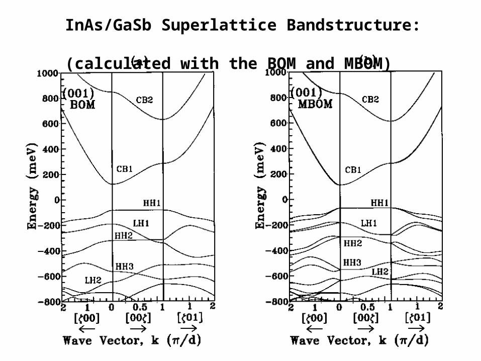
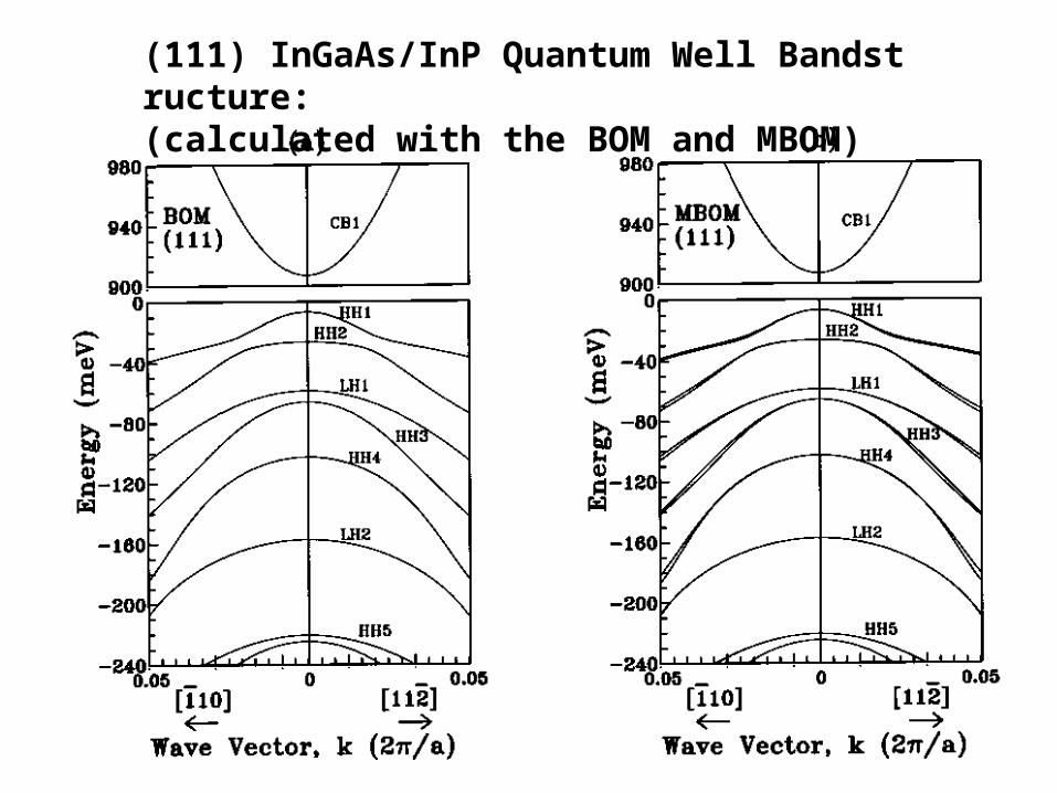
InAs/GaSb Superlattice Bandstructure:(calculated with the BOM and MBOM)
Orientation Dependence of InterfaceInversion Asymmetry Effect on InGaAs/InP Quantum Wells
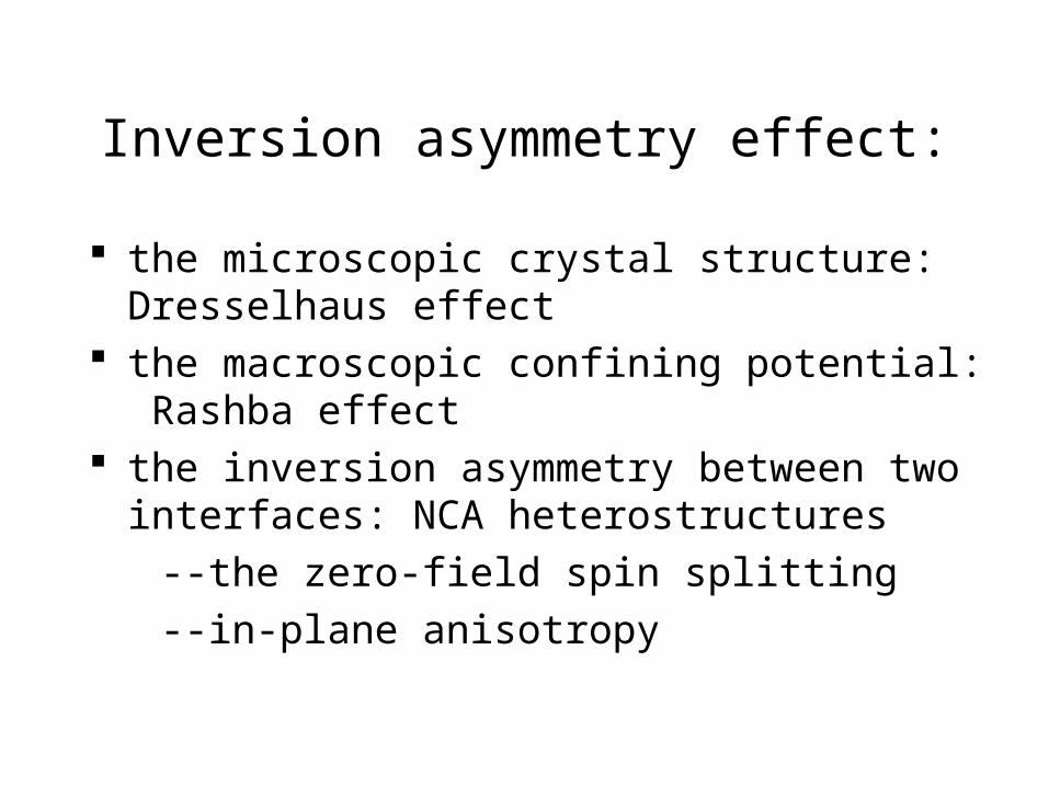
Inversion asymmetry effect:
the microscopic crystal structure: Dresselhaus effect
the macroscopic confining potential: Rashba effect the inversion asymmetry between two interfaces:
NCA heterostructures
--the zero-field spin splitting
--in-plane anisotropy
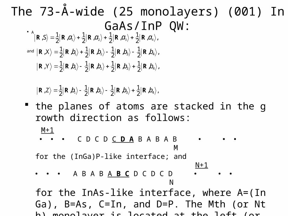
The 73-Å-wide (25 monolayers) (001) InGaAs/InP QW: A
and
the planes of atoms are stacked in the growth direction as follows: M+1 C D C D C D A B A B A B Mfor the (InGa)P-like interface; and N+1 A B A B A B C D C D C D N
for the InAs-like interface, where A=(InGa), B=As, C=In, and D=P. The Mth (or Nth) monolayer is located at the left (or right) interface, where N=M+25.
,,,,,, 4321 bbbb RRRRR 21
21
21
21X
,,,,,, 4321 bbbb RRRRR 21
21
21
21Y
,,,,,, 4321 aaaa RRRRR 21
21
21
21S
,,,,,, 4321 bbbb RRRRR 21
21
21
21Z
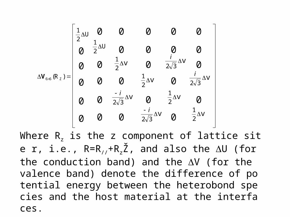
Where Rz is the z component of lattice site r, i.e., R=R//+RzŽ, and also the U (for the conduction band) and the V (for the valence band) denote the difference of potential energy between the heterobond species and the host material at the interfaces.
)R( Z66V
U2
1
0
0
0
0
0
U2
1
0
0
0
0
0
v32
i
v2
1
0
0
0
0
v2
1
v32
i
0
0
0
0 v2
1
v32
i
0
0
0
0 v2
1
v32
i
0
0
0
0
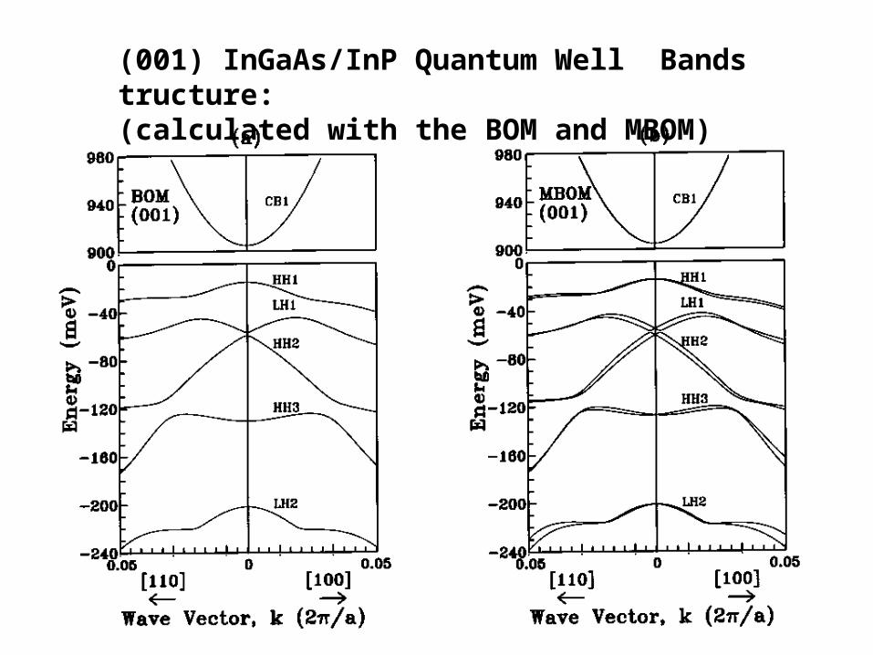
(001) InGaAs/InP Quantum Well Bandstructure:(calculated with the BOM and MBOM)
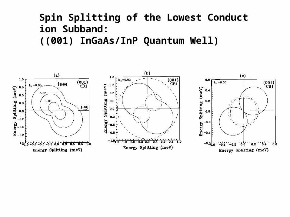
Spin Splitting of the Lowest Conduction Subband:((001) InGaAs/InP Quantum Well)
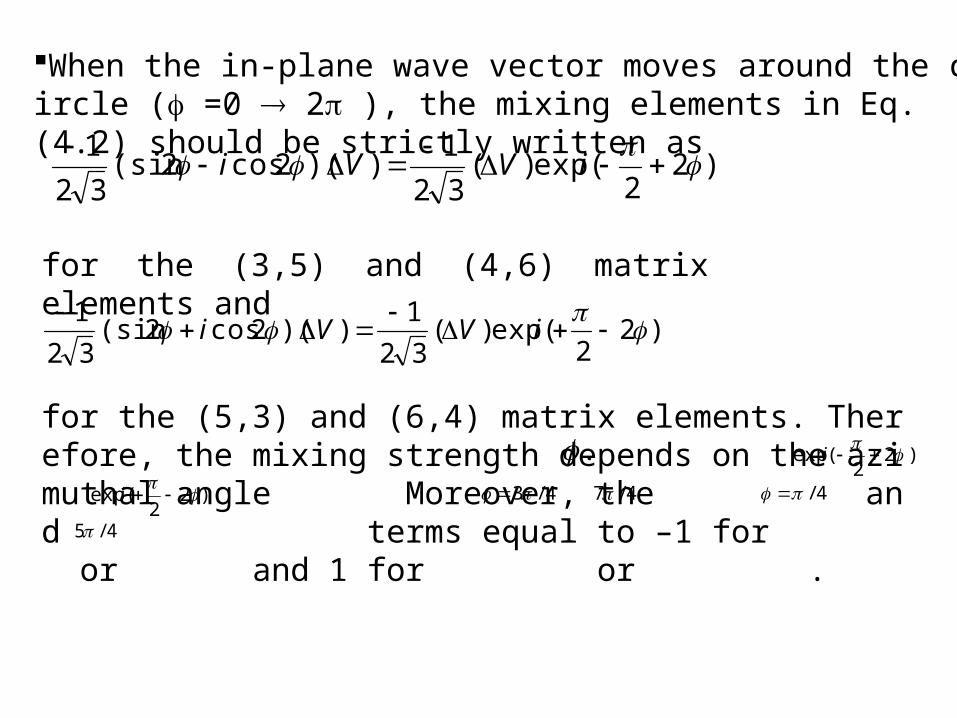
When the in-plane wave vector moves around the circle ( =0 2 ), the mixing elements in Eq. (4.2) should be strictly written as
)22
(exp)(32
1))(2cos2(sin
32
1
iVVi
for the (3,5) and (4,6) matrix elements and
)22
(exp)(32
1))(2cos2(sin
32
1
iVVi
for the (5,3) and (6,4) matrix elements. Therefore, the mixing strength depends on the azimuthal angle Moreover, the and terms equal to –1 for or and 1 for or .
. )22
(exp i
)22
(exp i 4/3 4/7 4/
4/5
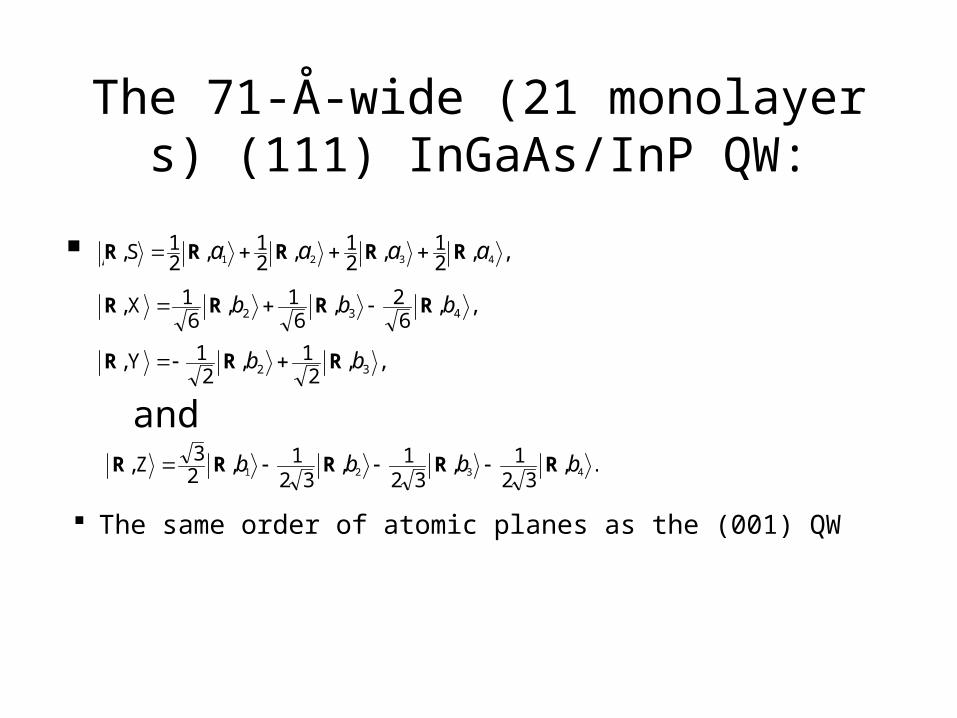
The 71-Å-wide (21 monolayers) (111) InGaAs/InP QW:
The same order of atomic planes as the (001) QW
A
and
,,,,X, 432 bbb RRRR62
61
61
,,,Y, 32 bb RRR21
21
.,,,,Z, 4321 bbbb RRRRR32
132
132
123
,,,,,, 4321 aaaa RRRRR 21
21
21
21S
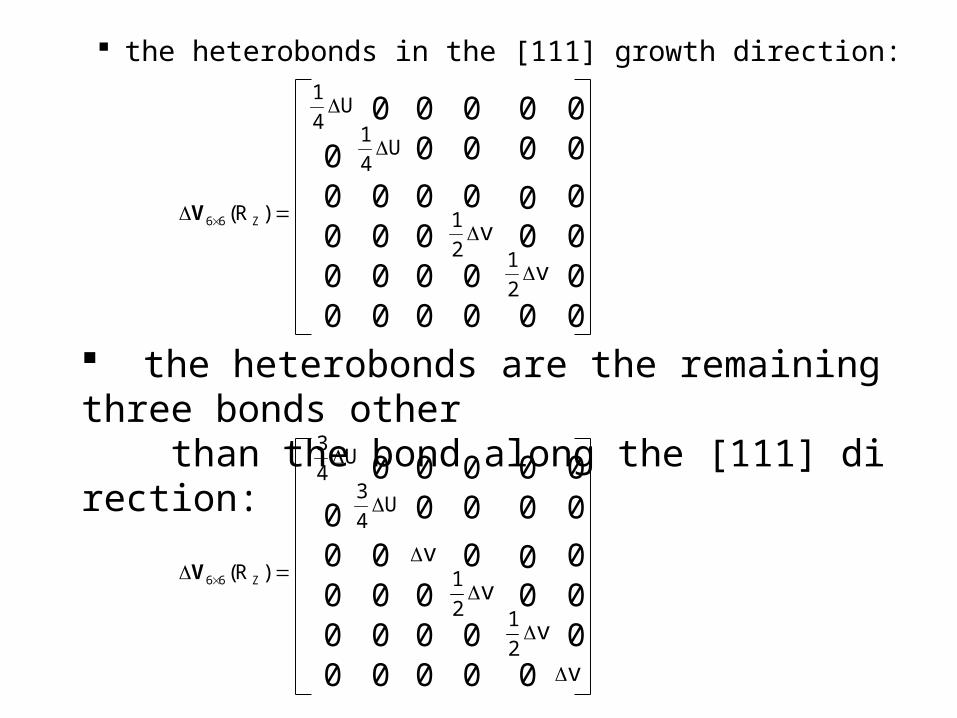
the heterobonds in the [111] growth direction:
the heterobonds are the remaining three bonds other than the bond along the [111] direction:
)R( Z66V
v2
1
00
0
0
0
v2
1
0
00
00
0
00
0
00
U4
1
0
0
000
00000
U4
1
0
00
0
00
)R( Z66V00
0
0
0
0
00
00
0
00
00
0
0
000
00000
00
0
00U
4
3
U4
3
v
v
v2
1
v2
1
(111) InGaAs/InP Quantum Well Bandstructure:(calculated with the BOM and MBOM)
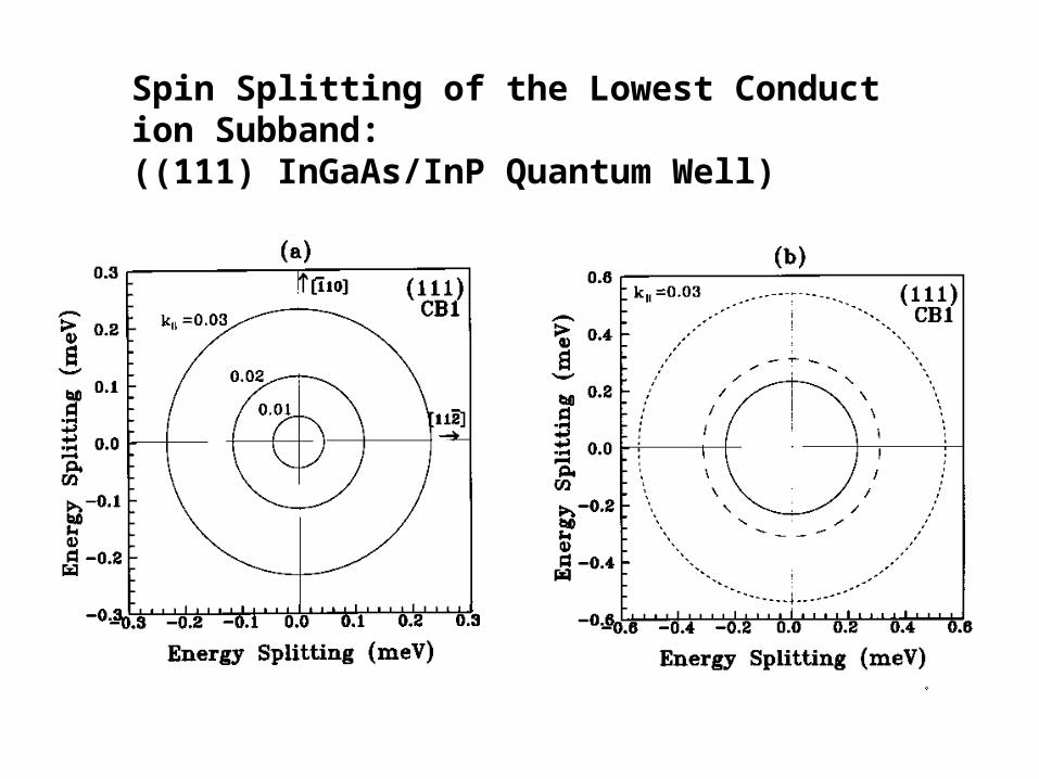
Spin Splitting of the Lowest Conduction Subband:((111) InGaAs/InP Quantum Well)
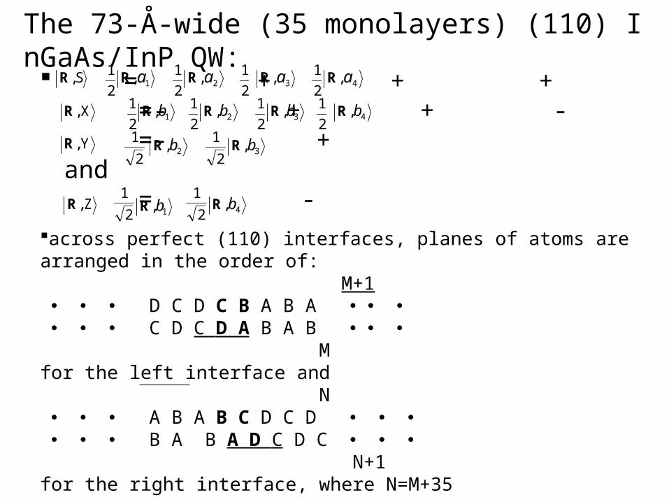
The 73-Å-wide (35 monolayers) (110) InGaAs/InP QW: = + + +
=- + + - =- +and = -
S,R2
11,aR
2
12,aR
2
13,aR
2
14,aR
X,R2
11,bR
2
12,bR
2
13,bR
2
14,bR
Y,R2
12,bR
2
13,bR
Z,R2
11,bR
2
14,bR
across perfect (110) interfaces, planes of atoms are arranged in the order of: M+1 D C D C B A B A C D C D A B A B Mfor the left interface and N A B A B C D C D B A B A D C D C N+1for the right interface, where N=M+35
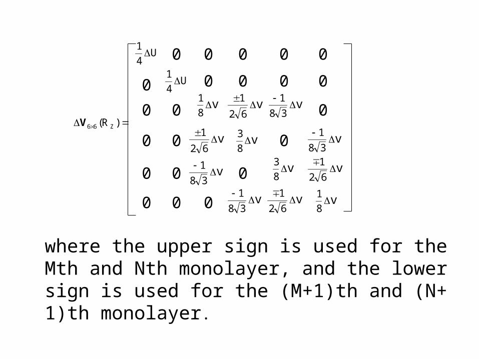
where the upper sign is used for the Mth and Nth monolayer, and the lower sign is used for the (M+1)th and (N+1)th monolayer.
)R( Z66V
0
0
0
0
0
0
0
0
0
U4
1
0
0
0
0
0
0
0
0
0
0
U4
1
0
0
0
v8
1
v62
1
v
8
3
v38
1
v38
1
v8
3v
38
1
v8
1 v
62
1
v38
1
v62
1
v62
1
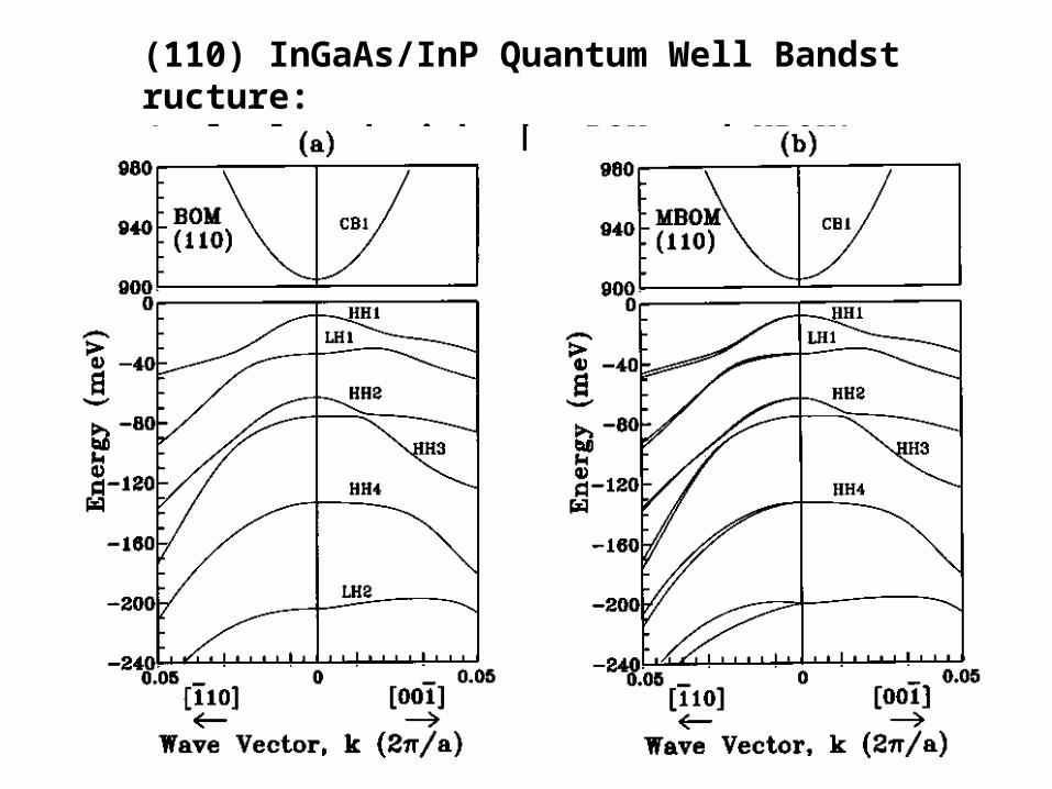
(110) InGaAs/InP Quantum Well Bandstructure:(calculated with the BOM and MBOM)
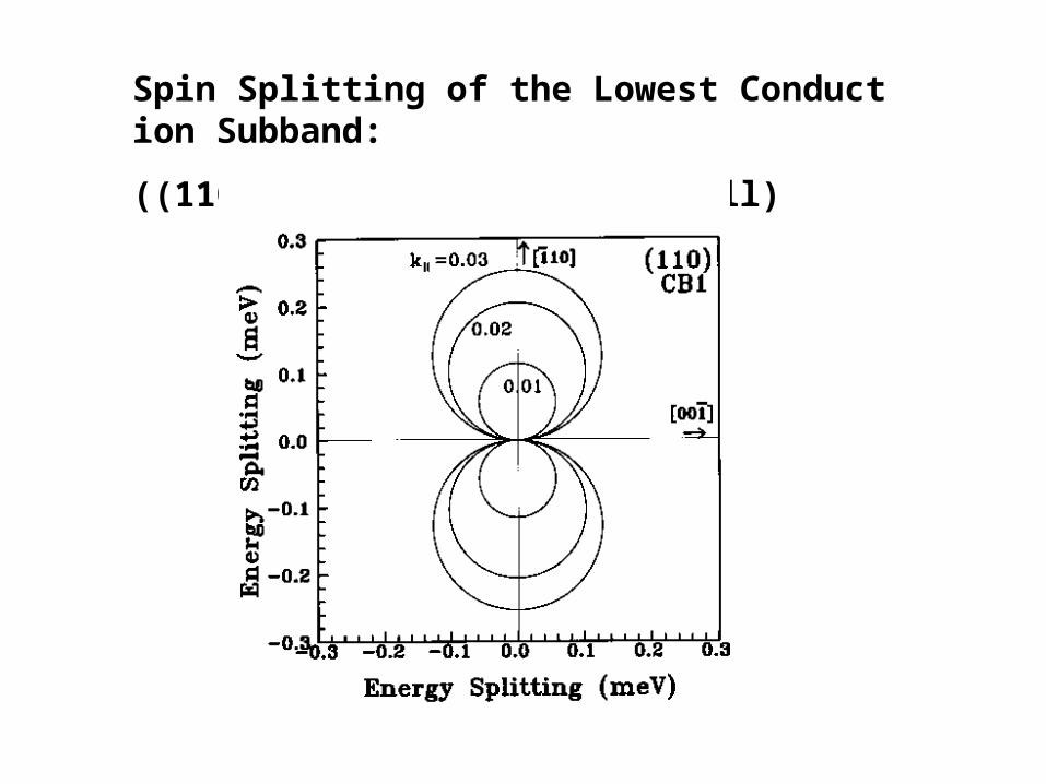
Spin Splitting of the Lowest Conduction Subband:
((110) InGaAs/InP Quantum Well)
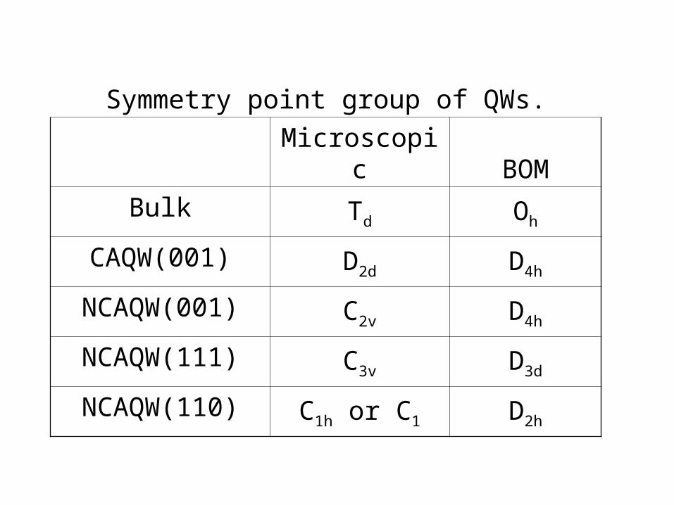
Symmetry point group of QWs.
Microscopic BOM
Bulk Td Oh
CAQW(001) D2d D4h
NCAQW(001) C2v D4h
NCAQW(111) C3v D3d
NCAQW(110) C1h or C1 D2h
Dresselhaus-like Spin Splitting
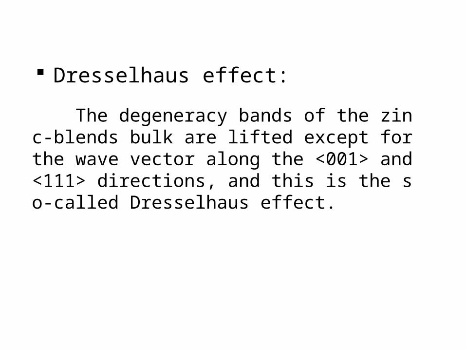
Dresselhaus effect:
The degeneracy bands of the zinc-blends bulk are lifted except for the wave vector along the <001> and <111> directions, and this is the so-called Dresselhaus effect.
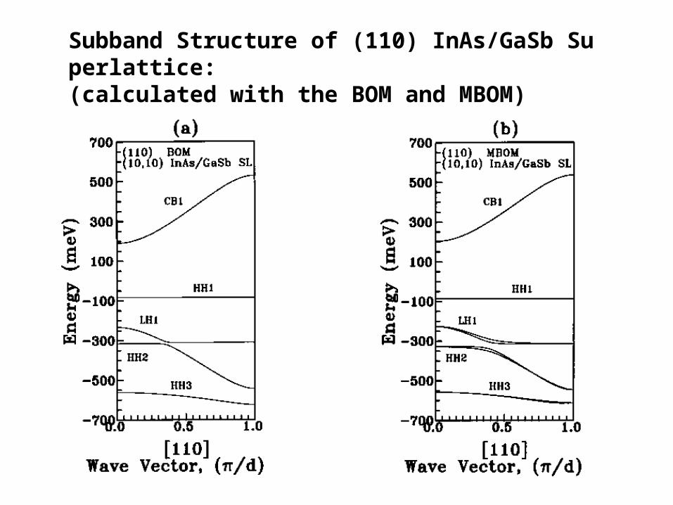
Subband Structure of (110) InAs/GaSb Superlattice:(calculated with the BOM and MBOM)
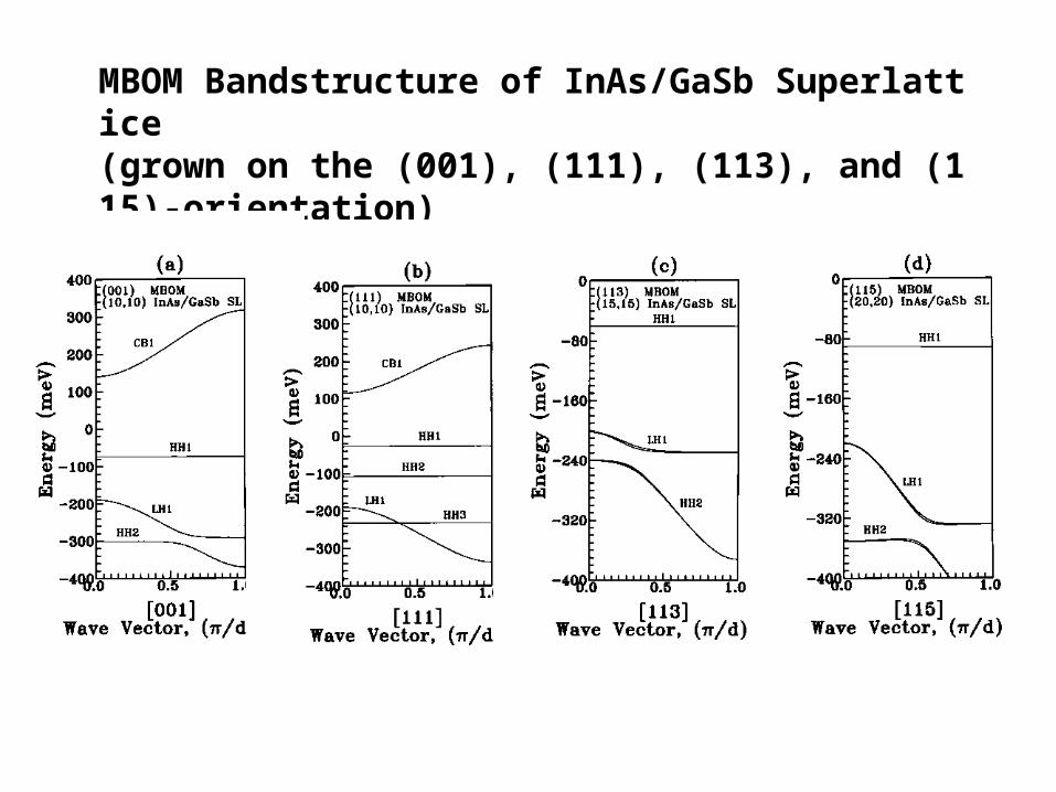
MBOM Bandstructure of InAs/GaSb Superlattice(grown on the (001), (111), (113), and (115)-orientation)
Microscopic Interface Effect on(Anti)crossing Behavior andSemiconductor-semimetal Transition inInAs/GaSb Superlattices
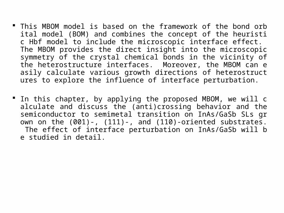
This MBOM model is based on the framework of the bond orbital model (BOM) and combines the concept of the heuristic Hbf model to include the microscopic interface effect. The MBOM provides the direct insight into the microscopic symmetry of the crystal chemical bonds in the vicinity of the heterostructure interfaces. Moreover, the MBOM can easily calculate various growth directions of heterostructures to explore the influence of interface perturbation.
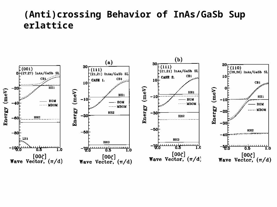
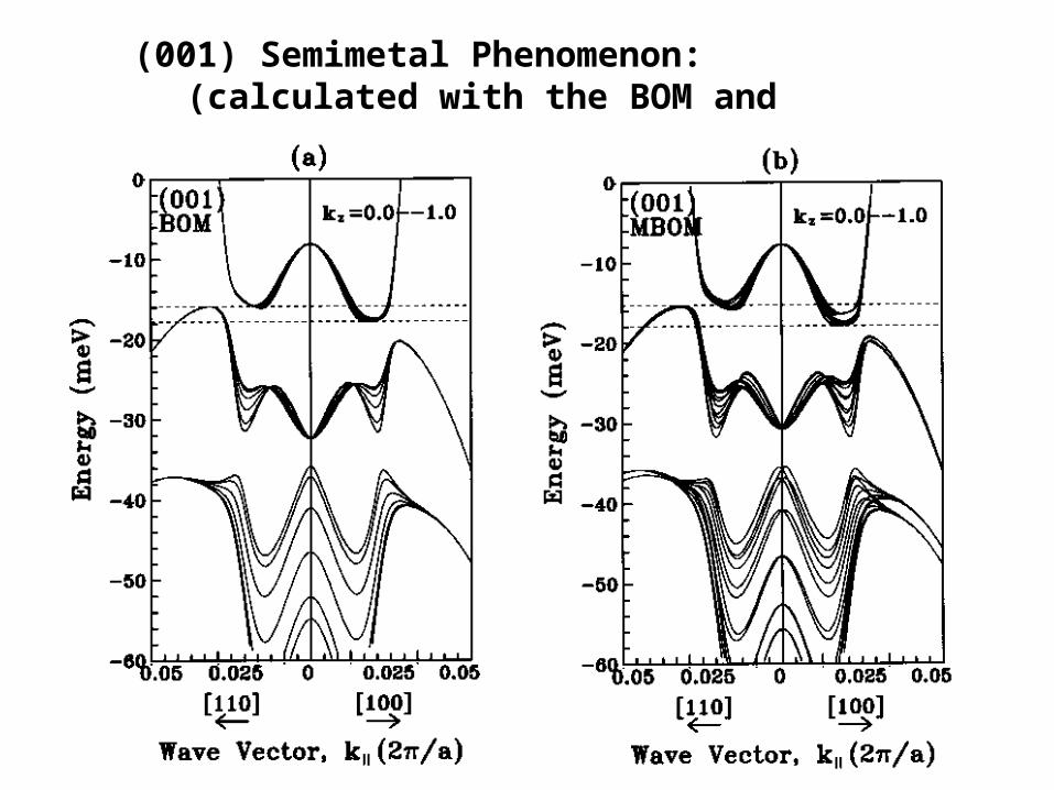
In this chapter, by applying the proposed MBOM, we will calculate and discuss the (anti)crossing behavior and the semiconductor to semimetal transition on InAs/GaSb SLs grown on the (001)-, (111)-, and (110)-oriented substrates. The effect of interface perturbation on InAs/GaSb will be studied in detail.
(Anti)crossing Behavior of InAs/GaSb Superlattice
(001) Semimetal Phenomenon:(calculated with the BOM and MBOM)
(111) Semimetal Phenomenon:(calculated with the BOM and MBOM)
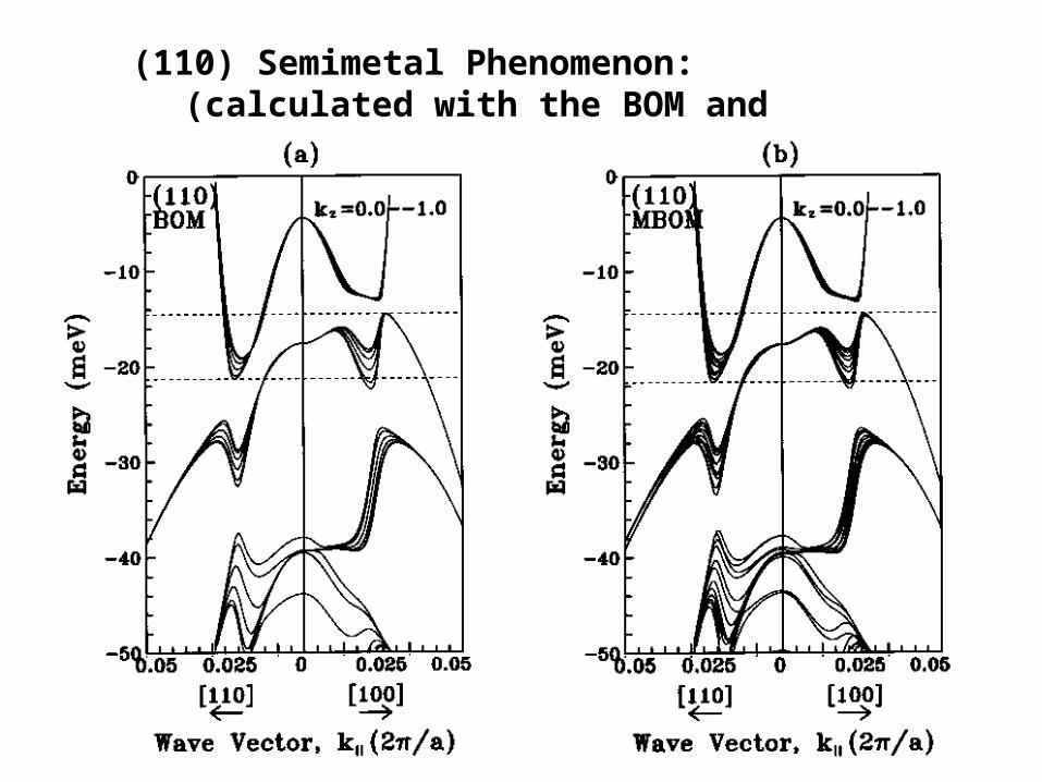
(110) Semimetal Phenomenon:(calculated with the BOM and MBOM)
k.p Finite Difference Method
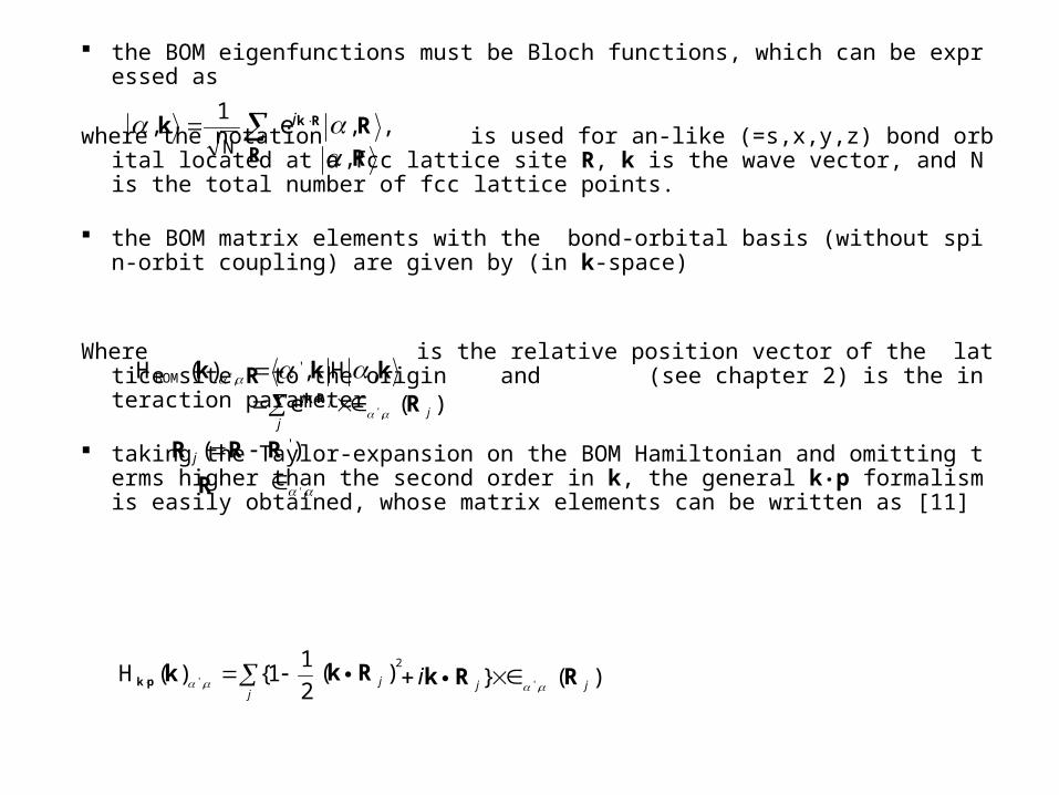
the BOM eigenfunctions must be Bloch functions, which can be expressed as
where the notation is used for an-like (=s,x,y,z) bond orbital located at a fcc lattice site R, k is the wave vector, and N is the total number of fcc lattice points.
the BOM matrix elements with the bond-orbital basis (without spin-orbit coupling) are given by (in k-space)
Where is the relative position vector of the lattice site R to the origin and (see chapter 2) is the interaction parameter
taking the Taylor-expansion on the BOM Hamiltonian and omitting terms higher than the second order in k, the general k‧p formalism is easily obtained, whose matrix elements can be written as [11]
,,1
, eN
Rk Rk
R
i
R,
kkk ,H,)(H ',BOM '
)(e,' j
i
j
j RRk
)( 'RRR j'R ,'
j 2
11{)(H
,' kpk
2)( jRk ).(}
,' jji RRk
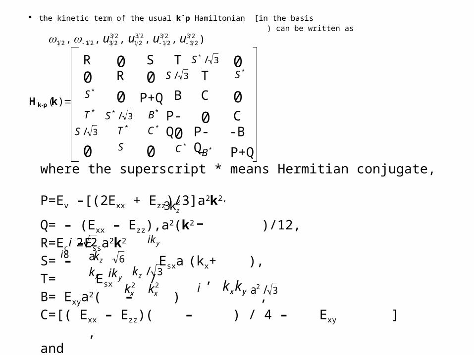
the kinetic term of the usual k˙p Hamiltonian [in the basis ) can be written as
,,, 23232121 u ),, 23
232321
2321 uuu
C
T
0
T
0
0S0
00
0
00
0
)(kH pk
*S
*T
3/S
3/*S*T
S
*B*C
3/S
*C
3/*S
*S
RR
P+Q B
P-Q P-
Q *B-
C-B
P+Qwhere the superscript * means Hermitian conjugate,P=Ev –[(2Exx + Ezz)/3]a2k2,
Q= – (Exx – Ezz),a2(k2- )/12, R=Ec –Essa2k2
S= – Esxa (kx+ ), T= Esx / , B= Exya2( – ) , C=[( Exx – Ezz)( – ) / 4 – Exy ] , andEc=Es + 12Ess, Ev=Ep + 8Exx + 4 Ezz.
2k3 z
22i yik
8izka 6
xk yik 3/zk2xk
2xk i yxkk 3/a 2
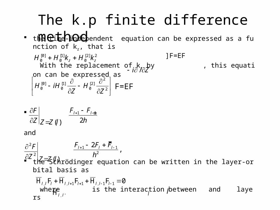
the time-independent equation can be expressed as a function of kz, that is ]F=EF
With the replacement of kz by , this equation can be expressed as
=
and
=
the Schrödinger equation can be written in the layer-orbital basis as
where is the interaction between and layers
2]2[0
]1[0
]0[0 zz kHkHH
Zi /
2
2]2[
0]1[
0]0[
0 ZH
ZiHH F=EF
)(lZZZ
F
h
FF ll
211
)(2
2
lZZZ
F
,
22
11
h
FFF lll
0FHFHFH 1111 ,,, lllllllll
',H ll l 'l
The k.p finite difference method
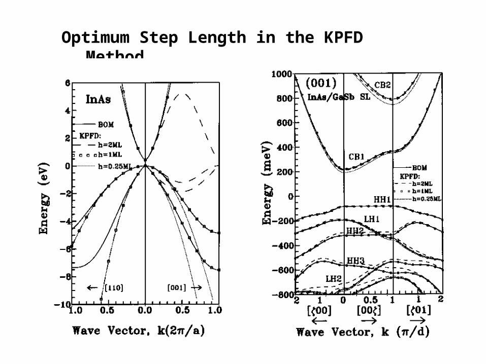
Optimum Step Length in the KPFD Method
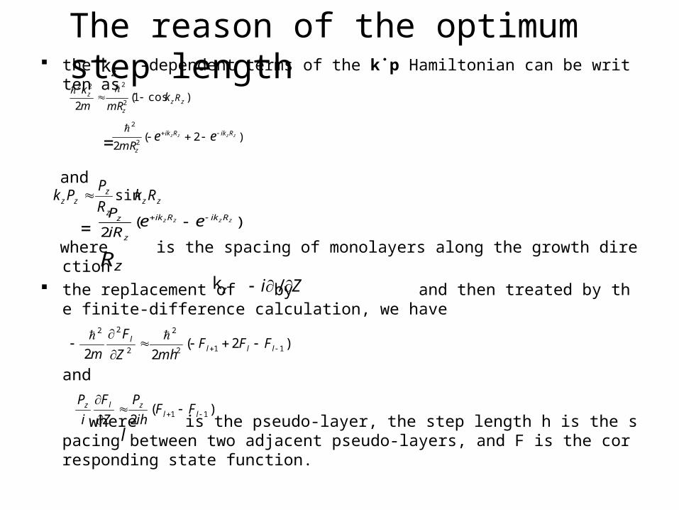
the -dependent terms of the k˙p Hamiltonian can be written as
and
where is the spacing of monolayers along the growth direction the replacement of by and then treated by the finite-difference cal
culation, we have
and
where is the pseudo-layer, the step length h is the spacing between two adjacent pseudo-layers, and F is the corresponding state function.
The reason of the optimum step lengthzk
zR
)cos1(2 2
222
zzz
z RkmRm
k
)2(2 2
2
zzzz RikRik
z
eemR
=
zzz
zzz Rk
R
PPk sin
),(2
zzzz RikRik
z
z eeiR
P =
zk Zi /
),(2 11
llzlz FFih
P
Z
F
i
P
)2(22 112
2
2
22
llll FFF
mhZ
F
m
l
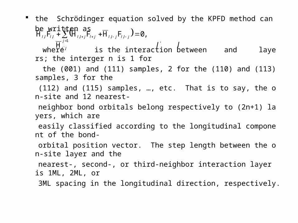
the Schrödinger equation solved by the KPFD method can be written as
where is the interaction between and layers; the interger n is 1 for
the (001) and (111) samples, 2 for the (110) and (113) samples, 3 for the
(112) and (115) samples, …, etc. That is to say, the on-site and 12 nearest-
neighbor bond orbitals belong respectively to (2n+1) layers, which are
easily classified according to the longitudinal component of the bond-
orbital position vector. The step length between the on-site layer and the
nearest-, second-, or third-neighbor interaction layer is 1ML, 2ML, or
3ML spacing in the longitudinal direction, respectively.
,0FHFHFH ,,
n
1,,,
jlljll
jjljllllll
ll ,'H 'l l
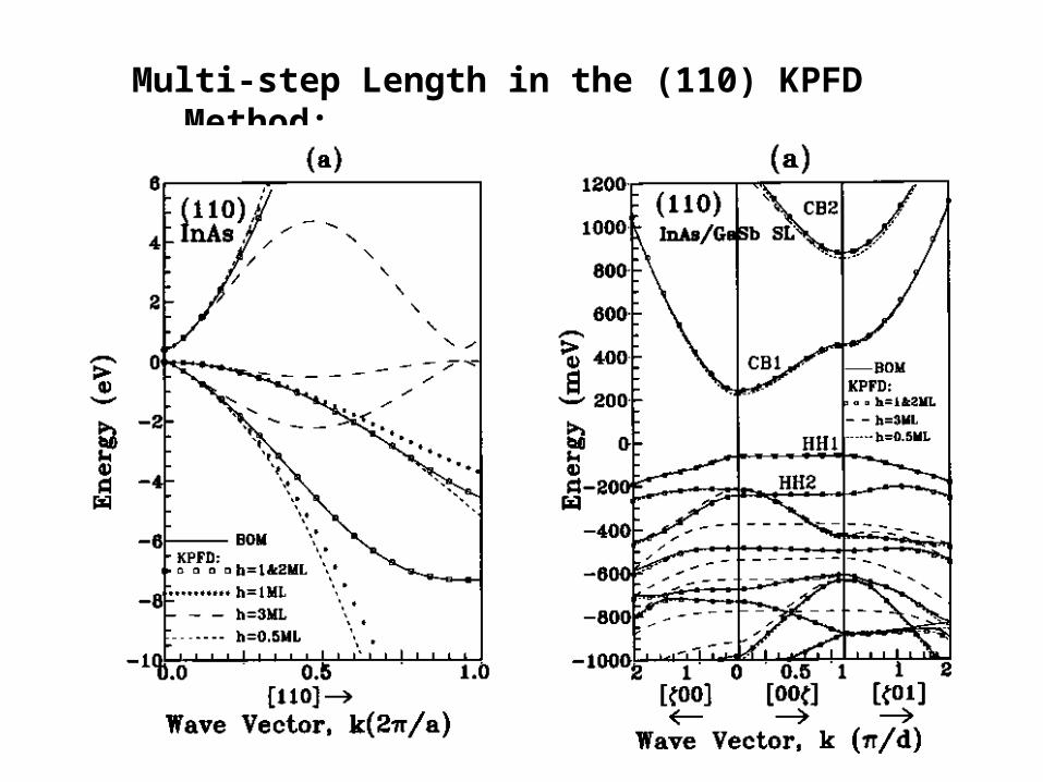
Multi-step Length in the (110) KPFD Method:
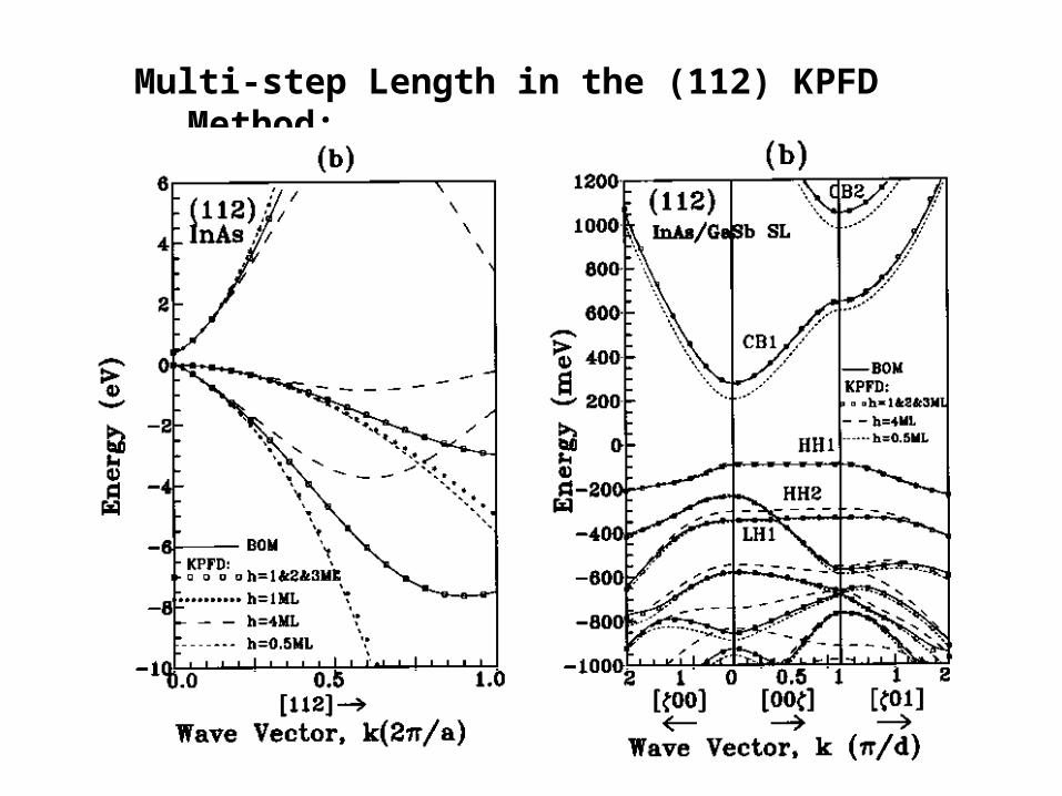
Multi-step Length in the (112) KPFD Method:
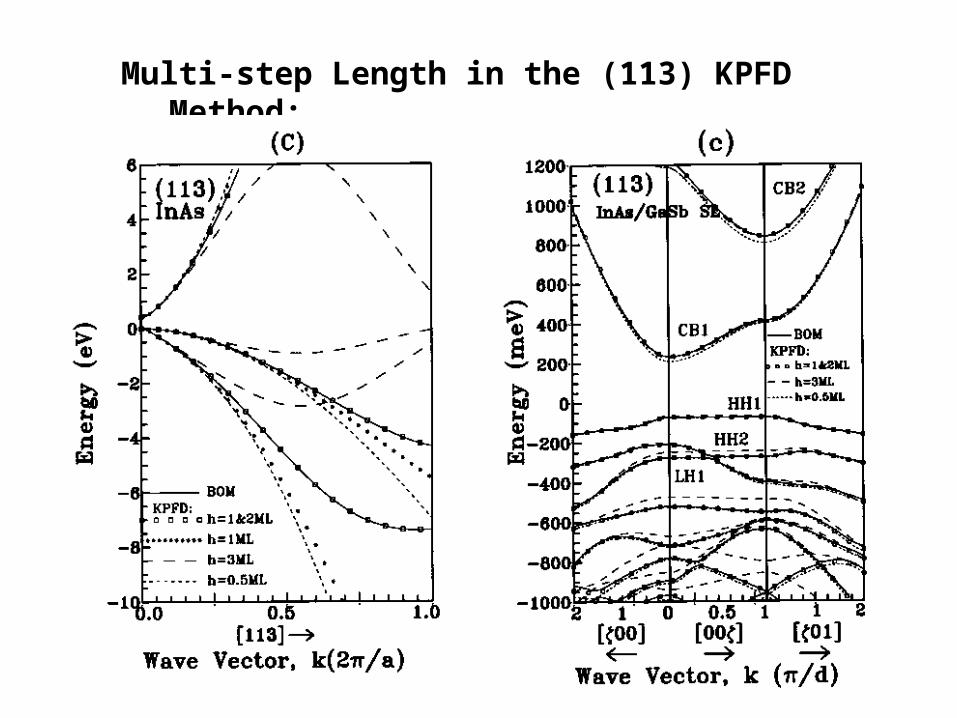
Multi-step Length in the (113) KPFD Method:
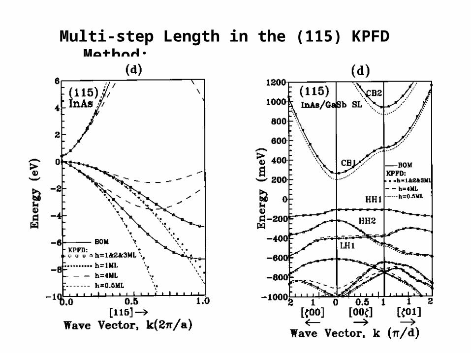
Multi-step Length in the (115) KPFD Method:
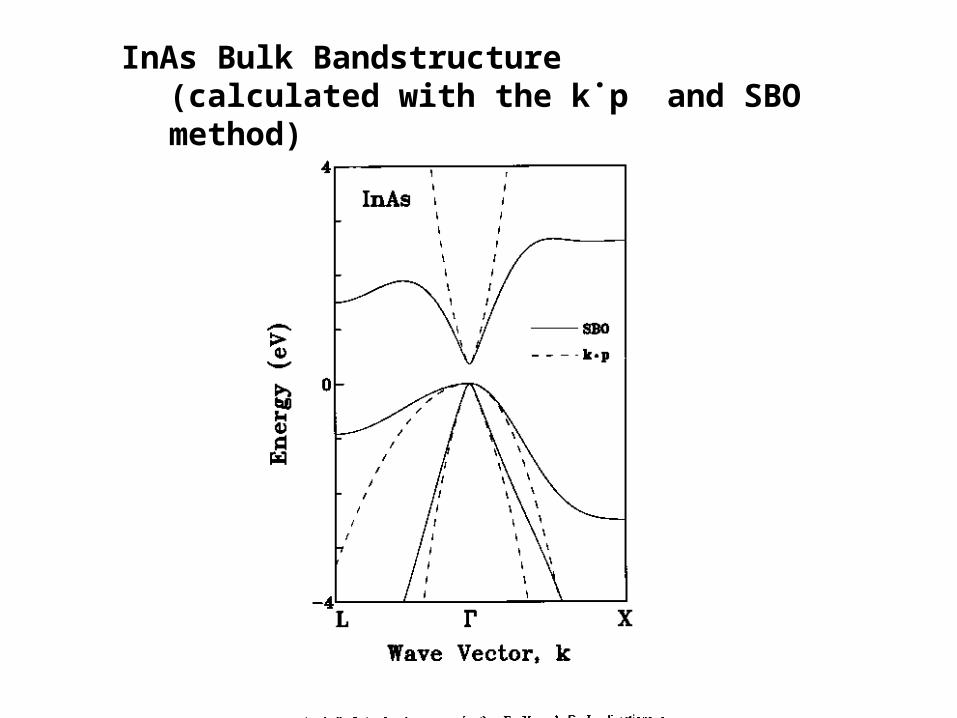
InAs Bulk Bandstructure(calculated with the k˙p and SBO method)
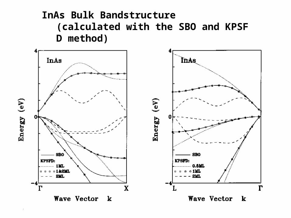
InAs Bulk Bandstructure(calculated with the SBO and KPSFD method)
Anisotropic Optical Matrix Elements inQuantum Wells with Various SubstrateOrientations
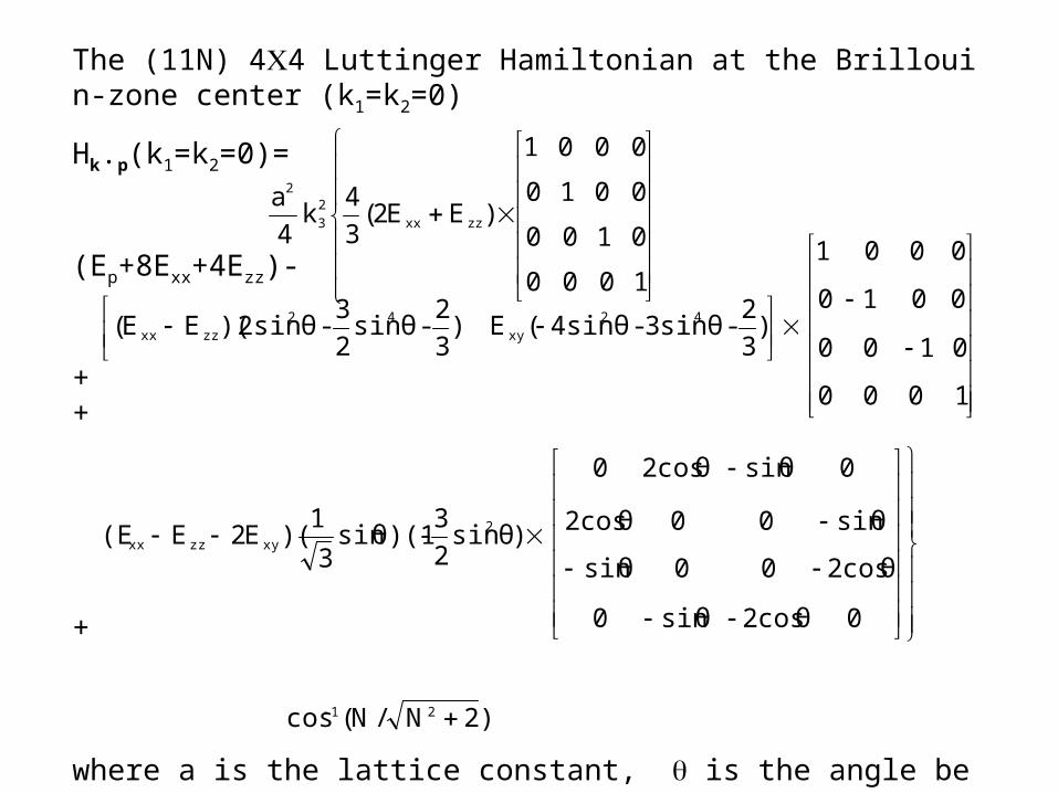
The (11N) 44 Luttinger Hamiltonian at the Brillouin-zone center (k1=k2=0)
Hk.p(k1=k2=0)=
(Ep+8Exx+4Ezz)-
+ +
+
where a is the lattice constant, is the angle between the z and X3 axes, which is equal to
1000
0100
0010
0001
)EE2(3
4k
4
azzxx
2
3
2
)
3
2-θsin
2
3-θsin2)(EE( 42
zzxx )
3
2-θsin3-θsin4(E 42
xy
1000
0100
0010
0001
)θsin2
3-θ)(1sin
3
1)(E2E(E 2
xyzzxx
0θcos2θsin0
θcos200θsin
θsin00θcos2
0θsinθcos20
).2N/N(cos 21
the optical transition matrix element between the conduction and the valence bands can be written as
where is the momentum operator and ê is the unit polarization vector.
the in-plane optical anisotropy can be calculated as
whereand are the squared matrix elements for the polarization parallel and perpendicular to , respectively.
i/
,ˆ Vi
eCM
,22
||
22
||
MM
MM
2
||M2
M]101[
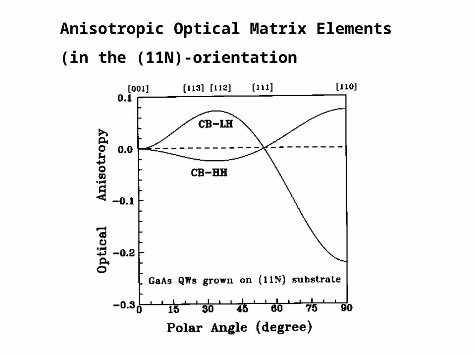
Anisotropic Optical Matrix Elements
(in the (11N)-orientation