Embed Size (px)
Citation preview

Time-to-Digital Converter Architecture
with Residue Arithmetic and its FPGA Implementation
Congbing Li Kentaroh Katoh Junshan Wang Shu Wu Shaiful Nizam Mohyar Haruo Kobayashi Division of Electronics and Informatics, Gunma University 1-5-1 Tenjin-cho Kiryu Gunma 376-8515 Japan
Phone: 81-277-30-1789 fax: 81-277-30-1707 e-mail: [email protected] Tsuruoka National College of Technology, Japan email: [email protected]
Abstract
This paper describes a time-to-digital converter (TDC) architecuture with residue arithmetic or Chinese Remainder theorem. It can reduce the hardware and power significantly compared to a flash type TDC while keeping comparable performance. Its FPGA implementation and measurement resuts show the effectiveness of our proposed architecture.
Keywords- Timing Measurement, Time to Digital
Converter, Residue, Chinese Remainder Theorem, FPGA
Introduction A Time-to-Digital-Converter (TDC) measures the time
interval between two edges, and time resolution of several picoseconds can be achieved when the TDC is implemented with an advanced CMOS process. TDC applications include phase comparators of all-digital PLLs, sensor interface circuits, modulation circuits, demodulation circuits, as well as TDC-based ADCs. The TDC will play an increasingly important role in the nano-CMOS era, because it is well suited to implementation with fine digital CMOS processes. [1,2,3].
There are various kinds of TDC circuits, and here we focus on a flash-typeTDC (Fig.1) [1]. It uses a delay line which consists of CMOS inverter buffer delays. Baesd on this flash-type TDC, we will introduce a new type TDC---Residue Arithmetic TDC to reduce the hardware and power significantly compared to a flash-type TDC while keeping comparable performance.Then we have implemtened it on an FPGA to verify the operation and performance.
Residue Arithmetic Suppose that m1,…,mr are positive integers and coprime
each other. Then there is unique positive interger x for given integers (a1,…,ar) which satisfy the following:
x ≡ ak (mod mk), k = 1, 2,…,r where 0≦ak< mk, 0≦x< N (N = m1·m2···mr). Table I shows the case of m1= 2, m2= 3, m3 = 5 and N=2x3x5=30, and we see that each k is mapped to residues of (m1, m2, m3 ) one to one [3,4].
Residue Arithmetic TDC Architecture We consider to use this residue arithmetic for TDC
implementation, because obtaining the residue is relatively easy for time signal (used in TDC design) while it is difficult for voltage signal. (used in ADC design). Fig.2 shows the proposed residue arithmetic TDC in the case of m1= 2, m2= 3, m3 = 5 and N=2x3x5=30, where the residues a (mod 2), b
Table I. An integer k and residues of (m1, m2, m3 ) m1 m2 m3 k m1 m2 m3 k
0 0 0 0 1 0 0 15
1 1 1 1 0 1 1 16
0 2 2 2 1 2 2 17
1 0 3 3 0 0 3 18
0 1 4 4 1 1 4 19
1 2 0 5 0 2 0 20
0 0 1 6 1 0 1 21
1 1 2 7 0 1 2 22
0 2 3 8 1 2 3 23
1 0 4 9 0 0 4 24
0 1 0 10 1 1 0 25
1 2 1 11 0 2 1 26
0 0 2 12 1 0 2 27
1 1 3 13 0 1 3 28
0 2 4 14 1 2 4 29
Fig 1. Flash-type TDC
Fig2. Proposed residue arithmetic TDC architecture.
- 104 - ISOCC2014978-1-4799-5127-7/$31.00 ⓒ2014 IEEE

(mod 3), c (mod 5) are obtained with ring oscNote that the proposed TDC uses only 10 d
flip-flops (because 2+3+5=10) while the corTDC requires 30 delay cells and 30 flip-flopproposed TDC uses M delay cells and M M=m1+m2+·+mr) while the corresponding uses N delay cells and N flip-flops (where Nand hence the circuit and power reduction TDC can be significant for a large N with pM<<N compared to the flash TDC.
FPGA Implementation
We have implemented our proposed TDC(Fig.3) [5, 6, 7], and Table II and Fig.4 showresults. We see that the proposed TDC wlinearity as expected.
Conclusion This paper describes residue arithmetic TD
implementation, and the measurement reoperation principle.
Acknowledgements We would like to thank STARC which supp
References
[1] S. Ito, S. Nishimura, H. Kobayashi, S. UemorT. Yamaguchi, K. Niitsu,“Stochastic TDC Self-Calibration,” IEEE Asia Pacific Confand Systems (Dec. 2010).
[2] K. Katoh, Y. Doi, S. Ito, H. Kobayashi, EKobayashi, “An Analysis of Stochastic Self-CUsing Two Ring Oscillators”, IEEE Asian(Nov. 2013).
[3] William A. Chren Jr., “Low-Area Edge SChinese Remainder Theorem”,IEEE T. InMeasurement 48(4): 793-797 (1999).
[4] http://www.ndl.go.jp/math/s1/c2.html [5] J. Xilinx, San Jose:“Virtex-5 LX FPGA M
Platform”,http://www.xilinx.com/products/bW-V5-ML501-UNI-G.htm.
[6] Xilinx, San Jose : “Virtex-5 user guide”Available: www.xilinx.com.
[7] Xilinx, “Using Xilinx ChipScope Pro ILA Navigator to Debug FPGA Applications”. [Owww.xilinx.com.
Fig.3 Proposed TDC implementation
cillators. delay cells and 10 rresponding flash ps; in general, the flip-flops (where flash-type TDC
N = m1·m2···mr), of the proposed
proper choice for
C with an FPGA w its measurement works with good
DC and its FPGA esults verify its
ports this project.
ri, Y. Tan, N. Takai, Architecture with
ference on Circuits
E. Li, N. Takai, O. Calibration of TDC n Test Symposium
Sampler Using the nstrumentation and
ML501 Evaluation boards-and-kits/H
”, 2010. [Online].
Core with Project Online]. Available:
Table II Measurement resultSample in Window
Elapsed
Time(ns) a b[0] b[
0 0.00 0 0 03 30.30 1 1 06 60.60 0 0 9 90.90 1 0 0
12 121.20 0 1 015 151.50 1 0 18 181.80 0 0 021 212.10 1 1 024 242.40 0 0 27 272.70 1 0 030 303.00 0 1 033 333.30 1 0 36 363.60 0 0 039 393.90 1 1 042 424.20 0 0 45 454.50 1 0 048 484.80 0 1 051 515.10 1 0 54 545.40 0 0 057 575.70 1 1 060 606.00 0 0 63 636.30 1 0 066 666.60 0 1 069 696.90 1 0 72 727.20 0 0 075 757.50 1 1 078 787.80 0 0 81 818.10 1 0 084 848.40 0 1 087 878.70 1 0
Fig.4 Measurement results of
on FPGA.
ts of the proposed TDC.
1] c[0] c[1] c[2] k
0 0 0 0 0 0 1 0 0 1 1 0 1 0 2 0 1 1 0 3 0 0 0 1 4 1 0 0 0 5 0 1 0 0 6 0 0 1 0 7 1 1 1 0 8 0 0 0 1 9 0 0 0 0 10 1 1 0 0 11 0 0 1 0 12 0 1 1 0 13 1 0 0 1 14 0 0 0 0 15 0 1 0 0 16 1 0 1 0 17 0 1 1 0 18 0 0 0 1 19 1 0 0 0 20 0 1 0 0 21 0 0 1 0 22 1 1 1 0 23 0 0 0 1 24 0 0 0 0 25 1 1 0 0 26 0 0 1 0 27 0 1 1 0 28 1 0 0 1 29
f the proposed TDC.
- 105 - ISOCC2014978-1-4799-5127-7/$31.00 ⓒ2014 IEEE

Kobayashi Lab.
Gunma University
Frequency Estimation Sampling Circuit
Using Analog Hilbert Filter
and Residue Number System
Yudai Abe, Shogo Katayama, Congbing Li,
Anna Kuwana, Haruo Kobayashi
Division of Electronics and Informatics
Gunma University
2019 13th IEEE International Conference on ASIC
A2-5 17:09 Xi’ An + Dalian Room October 30, 2019

2/25
OUTLINE
1. Research Background and Goal
2. Chinese Remainder Theorem
3. Proposed Waveform Sampling Circuit
4. Simulation Verification
5. Summary and Challenge
3/25
OUTLINE
1. Research Background and Goal
2. Chinese Remainder Theorem
3. Proposed Waveform Sampling Circuit
4. Simulation Verification
5. Summary and Challenge

4/25
Research Background
Next Generation Communication System “5G”
High frequencies
in communication systems
Electronic components
for high frequency bands
Communication speed
1980 1990 2000 2010 2020
1G2G
3G
3.5G
3.9G
4G
5G
2.4kbps
Higher than 10Gbps

5/25
Our Research Goal
High-frequency sampling circuit is difficult to realize
Sampling high frequency signal with multiple low frequency clocks
Use Aliasing proactively
Estimate high-frequency input signal
with multiple low-frequency clock sampling circuits
Analog Hilbert filter and residue number system
Our Approach :

6/25
OUTLINE
1. Research Background and Goal
2. Chinese Remainder Theorem
3. Proposed Waveform Sampling Circuit
4. Simulation Verification
5. Summary and Challenge

7/25
Chinese Remainder Theorem
Chinese arithmetic book ‘Sun Tzu calculation’
Generalization
Chinese Remainder Theorem
Answer 23
Sun Tzu calculation
Sun Tzu
“When dividing by 3, its residue is 2,
dividing by 5, its residue is 3,
dividing by 7,its residue is 2.
What is the original number ?”
孫子算経

8/25
How to use the Chinese remainder theorem
Sun Tzu
“How many soldiers are there?”
He used to quickly find out how many soldiers there are.
・・・
“Divide into 3 people.”

9/25
How to use the Chinese remainder theorem
Sun Tzu
“Divide into 3 people.”
・・・
Remainder : 2
He used to quickly find out how many soldiers there are.
“Divide into 5 people.”

10/25
How to use the Chinese remainder theorem
・・・
Remainder : 3Sun Tzu
“Divide into 5 people.”
He used to quickly find out how many soldiers there are.
“Divide into 7 people.”

11/25
“There are 23 people in all.”
How to use the Chinese remainder theorem
・・・
Sun Tzu
“Divide into 7 people.”
He used to quickly find out how many soldiers there are.
Remainder : 2

12/25
Example of Residue Number System
Residue number system
• Natural numbers
3, 5, 7 (relatively prime)
N=3×5×7=105
• k ( 0 <= k <= N-1 (=104))
a : Remainder of k dividing by 3 a=mod3(k)
b : Remainder of k dividing by 5 b=mod5(k)
c : Remainder of k dividing by 7 c=mod7(k)
a b c k
0 0 1 15
1 1 2 16
2 2 3 17
0 3 4 18
1 4 5 19
2 0 6 20
0 1 0 21
1 2 1 22
2 3 2 23
0 4 3 24
1 0 4 25
2 1 5 26
0 2 6 27
1 3 0 28
2 4 1 29
23 % 3 = 2, 23 % 5 = 3, 23 % 7 = 2
k (a, b, c)
one to one
Chinese remainder theorem

13/25
OUTLINE
1. Research Background and Goal
2. Chinese Remainder Theorem
3. Proposed Waveform Sampling Circuit
4. Simulation Verification
5. Summary and Challenge

14/25
Aliasing Phenomenon
A
t
Waveform frequency : 31kHz
f7kHz
𝐀𝟐
𝟐
1kHz 4kHz 8kHz
Sampling frequency : 8 kHz
Spectrums are folded
within the sampling frequency band
( sampling theorem )
Residue frequency
( 7 is the remainder of 31 divided by 8 )
FFT

15/25
Complex FFT of 𝑗 × sin 2𝜋𝑓𝑖𝑛𝑡
f7kHz1kHz4kHz 8kHz
f7kHz
1kHz
4kHz 8kHz
InvertResidue
frequency
Complex FFT
Input frequency : 31 kHz
Sampling frequency : 8 kHz
cosሺ2𝜋𝑓𝑖𝑛𝑡) 𝑗 × sin 2𝜋𝑓𝑖𝑛𝑡
Inverted spectrum
anti-symmetric at Nyquist frequency

16/25
Complex FFT of cosሺ2𝜋𝑓𝑖𝑛𝑡) + 𝑗 × sin 2𝜋𝑓𝑖𝑛𝑡
f7kHz
1kHz
4kHz 8kHz
InvertResidue
frequency
f7kHz1kHz 4kHz 8kHz
f7kHz1kHz
4kHz 8kHz
Residue
frequencyRemove
cosሺ2𝜋𝑓𝑖𝑛𝑡) 𝑗 × sin 2𝜋𝑓𝑖𝑛𝑡
cosሺ2𝜋𝑓𝑖𝑛𝑡) + 𝑗 × sin 2𝜋𝑓𝑖𝑛𝑡
+
Complex FFT
Input frequency : 31 kHz
Sampling frequency : 8 kHz
Extract spectrum
of the residual frequency

17/25
David Hilbert
(German mathematician)
1862-1943
RC polyphase filter
Use Analog Hilbert filter
𝐈𝐨𝐮𝐭 = 𝐀𝐜𝐨𝐬ሺ𝛚𝐭 + 𝛉)
𝐐𝐨𝐮𝐭 = 𝐀𝐬𝐢𝐧ሺ𝝎𝒕 + 𝜽)
𝐈𝐢𝐧 = 𝐜𝐨𝐬ሺ𝛚𝐭)
𝐐𝐢𝐧 = 𝟎
Polyphase
Filter
Generate in-phase and quadrature waves
from a single cosine wave
How Generate 𝑗 × sin 2𝜋𝑓𝑖𝑛𝑡

18/25
𝒇𝒊𝒏(Unknown)
Proposed Sampling Circuit
𝒇𝒓𝒆𝒔𝟑
𝒇𝒓𝒆𝒔𝟐
𝒇𝒓𝒆𝒔𝟏
RC
Polyphase
Filter
Sampling
circuit
Complex
FFT
Power
spectrum
Complex
FFT
Power
spectrum
Complex
FFT
Power
spectrum
Residue
number
system
𝐜𝐨𝐬ሺ𝟐𝝅𝒇𝒊𝒏𝒕)
𝐀𝐜𝐨𝐬ሺ𝟐𝝅𝒇𝒊𝒏𝒕 + 𝜽)
𝐀𝐬𝐢𝐧ሺ𝟐𝝅𝒇𝒊𝒏𝒕 + 𝜽)
𝒇𝒔𝟏Sampling frequency
Re1
Im1
Estimate
𝒇𝒊𝒏
Hilbert Filter
Generate
in-phase signal I
quadrature signal Q
Sampling frequencies:
relatively prime
Residue frequencies
Sampling
circuit
Re2
Im2
Sampling
circuit
Re3
Im3
𝒇𝒔𝟐
𝒇𝒔𝟑

19/25
OUTLINE
1. Research Background and Goal
2. Chinese Remainder Theorem
3. Proposed Waveform Sampling Circuit
4. Simulation Verification
5. Summary and Challenge

20/25
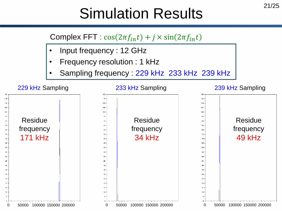
Simulation Settings
Complex FFT
Measurement at 20 GHz
using sampling frequencies of ≒ 200 kHz
• Input frequency : 12 GHz
• Frequency resolution : 1 kHz
• Sampling frequency : 229 kHz, 233 kHz, 239 kHz
( Relatively prime )
• Range of measurement : 0~2080622 kHz
( Note: 229 × 233 × 239 = 2080623 )
21/25
Simulation Results
229 kHz Sampling 233 kHz Sampling 239 kHz Sampling
50000 100000 150000 2000000 50000 100000 150000 2000000 50000 100000 150000 2000000
Residue
frequency
171 kHz
Residue
frequency
34 kHz
Residue
frequency
49 kHz
Complex FFT : cosሺ2𝜋𝑓𝑖𝑛𝑡) + 𝑗 × sin 2𝜋𝑓𝑖𝑛𝑡
• Input frequency : 12 GHz
• Frequency resolution : 1 kHz
• Sampling frequency : 229 kHz, 233 kHz, 239 kHz

22/25
Frequency Estimation by Residue Number System
a
[kHz]
b
[kHz]
c
[kHz]
k
[kHz]
0 0 0 0
1 1 1 1
2 2 2 2
┇ ┇ ┇ ┇
169 32 47 11999998
170 33 48 11999999
171 34 49 12000000
172 35 50 12000001
173 36 51 12000002
┇ ┇ ┇ ┇
226 230 236 12752320
227 231 237 12752321
228 232 238 12752322
Residue frequencies
171 kHz, 34 kHz, 49 kHz
Estimate input frequency 12GHz
Input frequency estimation
using residue frequencies
and residue number system

23/25
Simulation Result Overview
𝒇𝒊𝒏(Unknown)
𝟏𝟕𝟏𝒌𝑯𝒛
RC
Polyphase
Filter
Sampling
circuit
Complex
FFT
Power
spectrum
Complex
FFT
Power
spectrum
Complex
FFT
Power
spectrum
Residue
number
system
𝐜𝐨𝐬ሺ𝟐𝝅𝟏𝟐𝑮𝒕)
𝐀𝐜𝐨𝐬ሺ𝟐𝝅𝟏𝟐𝑮𝒕 + 𝜽)
𝐀𝐬𝐢𝐧ሺ𝟐𝝅𝟏𝟐𝑮𝒕 + 𝜽)
𝟐𝟐𝟗𝒌𝑯𝒛Sampling frequency
Re1
Im1
Estimate
𝒇𝒊𝒏 =𝟏𝟐𝑮𝑯𝒛
Sampling
circuit
Re2
Im2
Sampling
circuit
Re3
Im3
𝟐𝟑𝟑𝒌𝑯𝒛
𝟑𝟒𝒌𝑯𝒛
𝟐𝟑𝟗𝒌𝑯𝒛
𝟒𝟗𝒌𝑯𝒛
Estimate unknown input frequency
Hilbert Filter
24/25
OUTLINE
1. Research Background and Goal
2. Chinese Remainder Theorem
3. Proposed Waveform Sampling Circuit
4. Simulation Verification
5. Summary and Challenge

25/25
Summary and Challenge
● Proposed a method to estimate high-frequency signal
using multiple low-frequency sampling circuits.
● Confirmed its operation by theory and simulation.
● Measurable range is wide:
proportional to multiplication of multiple sampling frequencies.
● Estimated input frequency is discrete
Summary
Challenge
Consider estimation with fine frequency resolution

Thank you for your attention

Gunma University Kobayashi Lab
A Gray Code Based Time-to-Digital Converter Architecture
and its FPGA Implementation
Congbing Li Haruo Kobayashi
Gunma University

Outline
• Research Objective & Background
• Flash TDC and Problems
• Gray Code
• Gray Code TDC Architecture
• FPGA Implementation
• RTL Verification of Glitch-free Characteristic
• Conclusion

Research Objective
● Development of
Time-to-Digital Converter (TDC) architecture
with high-speed and small hardware
● Utilization of Gray code
Objective
Approach

Research Background
Voltage-domain resolution facing difficulties
due to reduced supply voltage
Voltage Resolution
Voltage
CMOS Scaling
Time Resolution
Time
CMOS Scaling
Time
Voltage
Time-domain resolution becoming superior
TDC measures time interval between two signal transitions, into digital signal.
(widely used in ADPLLs, jitter measurements, time-domain ADC)
TDC plays an important role in nano-CMOS era

Flash TDC
T
START
STOP
τ
τ
τ
τ τ τ
T
● Digital output (Dout)
proportional to time difference
between rising edges (T)
● Time resolution τ
Dout=2
Dout=1
Problems of Flash TDC
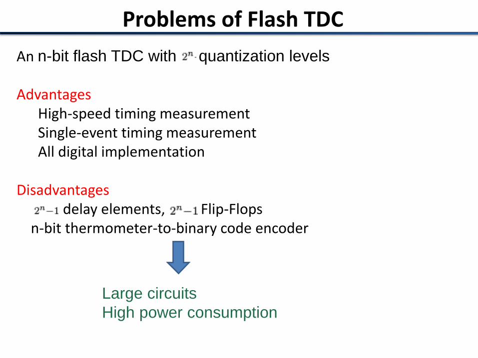
An n-bit flash TDC with quantization levels
Advantages High-speed timing measurement Single-event timing measurement All digital implementation Disadvantages delay elements, Flip-Flops n-bit thermometer-to-binary code encoder
Large circuits
High power consumption

Gray Code (1/2)
Gray Code a binary numeral system where two successive values
differ in only one bit
Decimal numbers
Binary Code Gray Code
0 0000 0000
1 0001 0001
2 0010 0011
3 0011 0010
4 0100 0110
5 0101 0111
6 0110 0101
7 0111 0100
8 1000 1100
9 1001 1101
10 1010 1111
11 1011 1110
12 1100 1010
13 1101 1011
14 1110 1001
15 1111 1000
Table. 4-bit Gray Code
For Gray code, between any two
adjacent numbers, only one bit
changes at a time
Gray code data is more reliable
compared with binary code

In a ring oscillator, between any two adjacent states, only one output changes at a time. This characteristic is very similar to Gray code.
8-stage Ring Oscillator Output 4-bit Gray Code
R0 R1 R2 R3 R4 R5 R6 R7 G3 G2 G1 G0
0 0 0 0 0 0 0 0 0 0 0 0
1 0 0 0 0 0 0 0 0 0 0 1
1 1 0 0 0 0 0 0 0 0 1 1
1 1 1 0 0 0 0 0 0 0 1 0
1 1 1 1 0 0 0 0 0 1 1 0
1 1 1 1 1 0 0 0 0 1 1 1
1 1 1 1 1 1 0 0 0 1 0 1
1 1 1 1 1 1 1 0 0 1 0 0
1 1 1 1 1 1 1 1 1 1 0 0
0 1 1 1 1 1 1 1 1 1 0 1
0 0 1 1 1 1 1 1 1 1 1 1
0 0 0 1 1 1 1 1 1 1 1 0
0 0 0 0 1 1 1 1 1 0 1 0
0 0 0 0 0 1 1 1 1 0 1 1
0 0 0 0 0 0 1 1 1 0 0 1
0 0 0 0 0 0 0 1 1 0 0 0
τ τ τ τ τ τ τ τR0 R1 R2 R3 R4 R5 R6 R7
For any given Gray
code, its each bit can
be generated by a
certain ring oscillator.
Gray Code (2/2)

Gray Code based TDC Architecture (1/2) A Gray code TDC architecture can be conceived by grouping a few ring oscillators
Figure. Proposed 6-bit Gray code TDC
MU
XM
UX
MU
X
Initial Value
START
STOP
τ τ
τ τ τ τ
τ τ τ τ τ τ τ τ
G0
G1
G2
DQ
DQ
DQ
MU
X τ τ τ τ
G3D
Q
MU
X τ τ τ τ
G4D
Q G5D
Q
8 buffers 8 buffers
16 buffers 16 buffers
Gray code
Decoder
B0
B1
B2
B3
Binary CodeGray Code
B4
B5
G0
G1
G2
G3
G4
G5

6-bit Gray Code
Binary Code
G5 G4 G3 G2 G1 G0(MSB) (LSB)
B5 B4 B3 B2 B1 B0(MSB) (LSB)
B5=G5B4=B5 G4B3=B4 G3B2=B3 G2B1=B2 G1B0=B1 G0
Figure. Gray code decoder
Gray Code based TDC Architecture (2/2)
Flash vs. Proposed TDCs
Flash TDC Proposed TDC
Number of delay elements
64
62
Number of Flip-flop
64
6
The maximum stage
64
32
for a measurement range of
significant hardware reduction
as # of bits increases.
for a measurement range of 26
2n

FPGA Implementation (1/3)
Proposed TDC implementation on Xilinx FPGA
START
InitialValue
B5 B4 B3 B2 B1 B0
Note: ADC is difficult to implement with full digital FPGA.

FPGA Implementation (2/3)
Measurement results of the proposed TDC with FPGA (6-bit case).
Proposed TDC operation is confirmed with FPGA evaluation.
0 40 80 120 160 200 240 280 320 360 400 440 480 520 560 600 6300
4
8
12
16
20
24
28
32
36
40
44
48
52
56
60
63
Elapsed Time (ns)
Output of Gray Code
TDC
Linear characteristics

FPGA Implementation (3/3)
Measurement results of the proposed TDC with FPGA (8-bit case)
0 160 320 480 640 800 960 1120 1280 1440 1600 1760 1920 2080 2240 2400 25500
16
32
48
64
80
96
112
128
144
160
176
192
208
224
240
255
Elapsed Time (ns)
Output of Gray Code
TDC
Linear characteristics
Similarly, 8-bit Gray code TDC architecture was implemented on FPGA.

RTL Verification of Glitch-free Characteristic (1/2)
• The proposed Gray code TDC can provide a glitch-free binary code sequence even there are mismatches between the delay stages.
• RTL simulation was conducted to verify this characteristic.
MU
XM
UX
MU
X
Initial Value
START
STOP
9.7 10
10 10 10 10
10 10 10 10 10 10 10 10
G0
G1
G2
DQ
DQ
DQ
MU
X 10 10 10 10
G3D
Q
MU
X 10 10 10 10
G4D
Q G5D
Q
8 buffers 8 buffers
16 buffers 16 buffers
Gray code
Decoder
B0
B1
B2
B3
Binary CodeGray Code
B4
B5
G0
G1
G2
G3
G4
G5
Simulated TDC with
delay mismatch

RTL Verification of Glitch-free Characteristic (2/2)
• RTL simulation result shows that no matter there are mismatches among the delay stages or not, the proposed Gray code TDC can always output a glitch-free binary code sequence.
0 40 80 120 160 200 240 280 320 360 400 440 480 520 560 600 6300
4
8
12
16
20
24
28
32
36
40
44
48
52
56
60
63
Elapsed Time (ns)
Output of Gray Code
TDC
No mismatch
Mismatches exist

Conclusion
We have proposed a gray code based TDC architecture - Comparable performance to Flash TDC - Significant hardware & power reduction We have implemented the proposed TDC with FPGA Confirmed its operation
Flash TDC Proposed TDC
Number of delay elements
Number of Flip-flop
The maximum stage
Significant hardware
reduction as # of bits
increases.
for a measurement range of 2n
2 2n
n
2n
2n
12n2n

Kobayashi Lab. Gunma
University
Gray-Code Input DAC Architecture for
Clean Signal Generation
Richen.Jiang, G.Adhikari, Yifei.Sun, Dan.Yao,
R.Takahashi, Y.Ozawa, N.Tsukiji, H.Kobayashi, R.Shiota
Gunma University, Socionext Inc.,
Nov. 9 NA-L2 8:30-9:50

2/44
OUTLINE
Research Background ・ ObjectiveGlitchesGray-codeGray-code Input DAC Architecture and OperationSimulation Verification by SPICEConclusion

3/44
OUTLINE
Research Background ・ ObjectiveWhat are GlitchesGray-codeGray-code Input DAC Architecture and OperationSimulation Verification by SPICEConclusion

4/44
Research Background
Analog Input Analog Input
DigitalSignal
Processing

5/44
Research Background
Basic architecture of DAC
Current Source DAC Capacitive DAC Resistance DAC
The switch is driven with a binary code glitch

6/44
Research Objective
Objective
Design Digital-to-Analog Converter (DAC) architectures for clean signal generation
Approach
By reducing glitches with Gray-Code input topologies

7/44
OUTLINE
Research Background ・ ObjectiveGlitchesGray-codeGray-code Input DAC Architecture and OperationSimulation Verification by SPICEConclusion

8/44
What are Glitches
Voltage spikes
Reasons for glitchesDecimal numbers Natural Binary code
0 0 0 0 0
1 0 0 0 1
2 0 0 1 0
3 0 0 1 1
4 0 1 0 0
5 0 1 0 1
6 0 1 1 0
7 0 1 1 1
8 1 0 0 0
9 1 0 0 1
10 1 0 1 0
11 1 0 1 1
12 1 1 0 0
13 1 1 0 1
14 1 1 1 0
15 1 1 1 1
when7→8
0111→0110→0100→0000→1000
when8→7
1000→1001→1011→1111→0111
The most significant bit (MSB) changes (near the middle point)
9/44
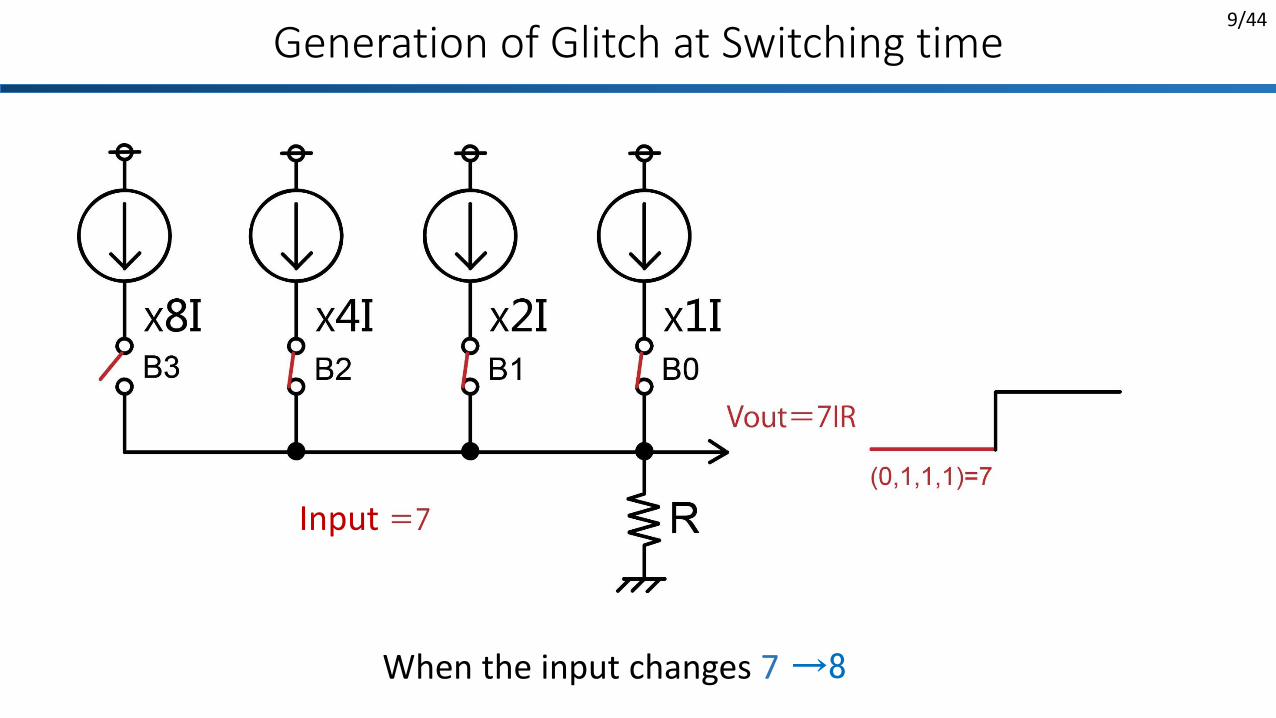
Generation of Glitch at Switching time
Input
When the input changes 7 →8
10/44
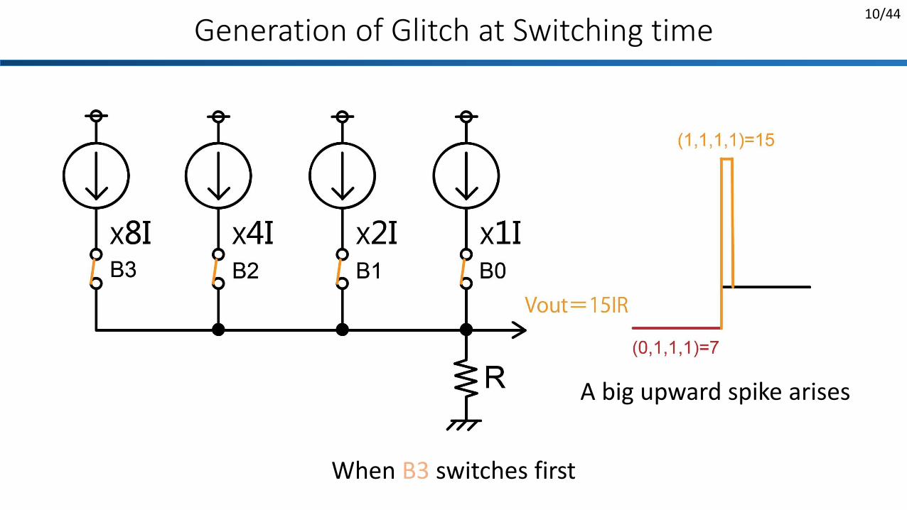
Generation of Glitch at Switching time
When B3 switches first
A big upward spike arises

11/44
Generation of Glitch at Switching time
When B3 switches last
A big downward spike occur

12/44
Generation of Glitch at Switching time
Input
glitch
glitch

13/44
Glitch Problem and Remedy
Effects of Glitch
Serious deterioration of images, videos, sounds
Remedy
Using high-order reconstruction filterUsing track/hold circuitry at the DAC output
Using Gray-Code input DAC topologies
Extra Space in IC, Expensive
14/44
OUTLINE
Research Background ・ ObjectiveWhat are GlitchesGray-codeGray-code Input DAC Architecture and OperationSimulation Verification by SPICEConclusion

15/44
Gray-Code
Binary to Gray code converterBinary to Gray code conversion diagram
Two adjacent number Only one bit change
Gray-Code Alternative representation of binary code
(Gn=Bn+1⊕Bn)

16/44
Gray Code
Compare with Binary code and Gray code
Binary code Multiple bits change at a time
Trigger more switches
Example. 1 2 --- 0001 0010 2 bits change
7 8--- 0111 1000 all 4 bits change
Gray code Only one bit changes at a time
Triggers one switch
Example. 1 2 --- 0001 0011 one bit change 7 8 --- 01001100 one bit change
Less glitches
17/44
OUTLINE
Research Background ・ ObjectiveWhat are GlitchesGray-codeGray-code Input DAC Architecture and OperationSimulation Verification by SPICEConclusion

18/44
Gray-code Input DAC Architecture and Operation
1.Current-steering Gray-Code DAC
2.Charge-mode Gray-Code DAC
3.Voltage-mode Gray-Code DAC

19/44
Current/Voltage Switch Matrix
Parallel connection Cross connection
When S=0 When S=1
When S=0 When S=1
Switch is DPDT (Double-Pole Double-Throw)

20/44
1.Current-steering Gray-Code DAC
Conventional Binary-Weighted current-steering DAC
Gray-Code input current-steering DAC

21/44
Code Conversion
Binary code Gray code Current switch matrix for Gray code
Binary code domain Gray code domain
Code domain in Gray-code input current-steering DAC

22/44
A Gray-code input current-steering DAC (data=5)
𝐼𝑜𝑢𝑡+ = 𝐼 − 2𝐼 + 4𝐼 − 8𝐼 = −5𝐼
𝐼𝑜𝑢𝑡− = −𝐼 + 2𝐼 − 4𝐼 + 8𝐼 = 5𝐼𝐼𝑜𝑢𝑡 = (𝐼𝑜𝑢𝑡+) − 𝐼𝑜𝑢𝑡− = −10𝐼

23/44
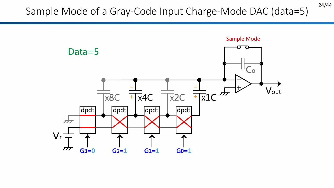
2.Charge-mode Gray-code DAC
A binary-weighted capacitor DAC A Gray-code input charge-mode DAC
24/44
Sample Mode of a Gray-Code Input Charge-Mode DAC (data=5)

25/44
Sample Mode of a Gray-Code Input Charge-Mode DAC (data=5)

26/44
3.Voltage-mode Gray-Code DAC

27/44
A Gray-Code Input Voltage-mode DAC (data=5)
𝑉𝑜𝑢𝑡+ = 𝑉𝑟 + 4𝑉𝑟 = 5𝑉𝑟

28/44
OUTLINE
Research Background ・ ObjectiveWhat are GlitchesGray-codeGray-code Input DAC Architecture and OperationSimulation Verification by SPICEConclusion

29/44
Simulation Verification by SPICE
1.Simulation of current-steering Gray-Code DAC
2.Simulation of charge-mode Gray-Code DAC
3.Simulation of voltage-mode Gray-Code DAC
4.Verification of glitch reduction

30/44
1.SPICE Realization of Current-Steering of Gray-Code Input
SubtractorCircuit
Latch
Gray-Code
Binary-Code

31/44
1.Simulation of current-steering Gray-Code DAC
4bit Current-steering DAC 8bit Current-steering DAC

32/44
2.SPICE Realization of charge-mode of Gray-Code Input
Non-overlapclock Latch
Gray-Code
Binary-Code

33/44
2. Simulation of charge-mode Gray-Code DAC
4bit Charge-mode DAC 8bit Charge-mode DAC

34/44
3.SPICE Realization of Voltage-mode of Gray-Code Input
AdderCircuit
AdderCircuit
AdderCircuit
Latch
Gray-Code
Binary-Code

35/44
3. Simulation of Voltage-mode Gray-Code DAC
4bit Voltage-mode DAC 8bit Voltage-mode DAC

36/44
4.Verification of glitch reduction
Binary code generating circuit
Conventional Current-Steering DAC with switching delay (8bit)

37/44
4.Verification of glitch reduction
SubtractorCircuit
Binary code generating circuit
Current-Steering Gray-code input DAC with switching delay (8bit)

38/44
4.Simulation Result (Up Sweeping)
Conventional Current-Steering DAC
Current-steering DAC of Gray-code
glitch
Conventional Current-Steering DAC VS. Current-steering DAC of Gray-code

39/44
4.Simulation Result (Down Sweeping)
Conventional Current-Steering DAC
Conventional Current-Steering DAC VS. Current-steering DAC of Gray-code
Current-steering DAC of Gray-code
glitch

40/44
4.Simulation Result (Random Switching Delay)
Conventional Current-Steering DAC VS. Current-steering DAC of Gray-code

41/44
OUTLINE
Research Background ・ ObjectiveWhat are GlitchesGray-codeGray-code Input DAC Architecture and OperationSimulation Verification by SPICEConclusion

42/44
Conclusion
Binary codeDAC Converter using Glitch
Gray code
input
DAC Converter using Gray code input
Current-steering Gray-Code DACCharge-mode Gray-Code DACVoltage-mode Gray-Code DAC
Glitch reduction
deterioration

43/44
Final statement
• Coding method can lead to robust mixed-signal circuit design.
Gray code was invented by Frank Gray at Bell Lab in 1947.

Thank you for listening
谢谢
44/44

Study of Gray Code Input DAC for Glitch Reduction
*Adhikari Gopal Richen Jiang Haruo Kobayashi
Kobayashi Laboratory, Gunma University, Japan
1

Outline oResearch Objective
oIntroduction to DAC
oGlitches
oIntroduction to Gray Code
oGray Code Input DAC oSwitch Matrix Design
oVoltage Mode Gray Code Input DAC
oCurrent Steering Mode Gray Code Input DAC
oConclusion
2 ICSICT 2016 Paper ID : S0346

Research Objective Research and implement DAC for glitch reduction using Gray code input
Approach
Use MOSFETs for DAC design
Utilization of Gray code input for glitch reduction
3 ICSICT 2016 Paper ID : S0346
*(difficult to design)

Introduction to DAC •Convert digital signal to analog signal
•Signal to be recognized by human senses
•Widely used in signal processing
4 ICSICT 2016 Paper ID : S0346

What are Glitches ? Voltage spikes
Reasons for glitches ◦Capacitive coupling ◦Differences in switching
Glitch behaviour Dominated by difference in switching
Switching of MSB Most significant glitches
(Multiple switches changing states at once)
5 ICSICT 2016 Paper ID : S0346

Glitch Problem and Remedy Effects of Glitch
oSerious deterioration of images, videos and sounds
Remedy ◦ Using high-order reconstruction filter ◦ Using track/hold circuitry at the DAC output
◦Using Gray code input DAC topologies
Extra Space in IC, Expensive
6 ICSICT 2016 Paper ID : S0346

What is Gray code ? oGray code Alternative representation of binary code
oTwo adjacent numbers Only one bit change
oReflected binary code
Binary to Gray code conversion
7 ICSICT 2016 Paper ID : S0346
Binary to Gray code converter

Gray Code versus Binary Code Binary code Multiple bits change at a time
Trigger more switches
Example. 1 2 --- 0001 0010 2 bits change
7 8--- 0111 1000 all 4 bits change
Gray code Only one bit changes at a time
Triggers one switch Example. 1 2 --- 0001 0011 one bit change (B2)
7 8 --- 01001100 one bit change (B4)
Less glitches
Decimal Binary Gray 0 0000 0000
1 0001 0001
2 0010 0011
3 0011 0010
4 0100 0110
5 0101 0111
6 0110 0101
7 0111 0100
8 1000 1100
9 1001 1101
10 1010 1111
11 1011 1110
12 1100 1010
13 1101 1011
14 1110 1001
15 1111 1000
8 ICSICT 2016 Paper ID : S0346

Gray code versus Binary code Timing Diagram
9 ICSICT 2016
Gray code timing diagram Binary code timing diagram
Gray code Only one bit changes at a time 00010011 Binary code Multiple bits change at a time 00010010 Using Gray code Less glitches expected to appear
Paper ID : S0346

Gray Code Input DAC
10 ICSICT 2016

Switch is DPDT (Double-Pole Double-Throw)
Switch Matrix Design
11 ICSICT 2016 Paper ID : S0346

Switch Matrix Operation
12 ICSICT 2016
CTL LOW: M3 , M4 ON, M1, M2 OFF IN1 = OUT1, IN2 = OUT2
CTL HIGH: M1, M2 ON, M3, M4 OFF IN1 = Out2 , IN2 =OUT1
Paper ID : S0346

Voltage Mode Gray Code Input DAC oIN1 = Vref
oIN2 = 0
oCTL Gray code input
oOUT1, OUT2 Connected with R-2R Ladder
oFinal stage terminated with 1.5R, 0.5R resistors.
𝑉𝑜𝑢𝑡(𝐷) =𝑉𝑟𝑒𝑓
2𝑛+1 | 2𝐷 − 1 |
n : number of bits D =1, 2, 3...n+1
13 ICSICT 2016 Paper ID : S0346

Voltage Mode Gray Code Input DAC SPICE Simulation Results
D Bits Vout
1 0000 3/32 0.09375
2 0001 9/32 0.28125
3 0011 15/32 0.46875
4 0010 21/32 0.65625
5 0110 27/32 0.84375
6 0111 33/32 1.03125
7 0101 39/52 1.21875
8 0100 45/32 1.40625
9 1100 51/32 1.59375
10 1101 57/32 1.78125
11 1111 63/32 1.96875
12 1110 69/32 2.15625
13 1010 75/32 2.34375
14 1011 81/32 2.53125
15 1001 87/32 2.71875
16 1000 93/32 2.90625
14 ICSICT 2016 Paper ID : S0346
4-bit case

Voltage Mode Gray Code Input DAC SPICE Simulation Results
15 ICSICT 2016 Paper ID : S0346
8-bit case

Voltage Mode Gray Code Input DAC MOSFET Implementation
Aspect ratios W/L for R, 2R, 1.5R, 0.5R
𝑅 =𝑉𝐷𝑆
𝐼𝑑𝑠𝑎𝑡=
𝑉𝐷𝑆𝑢𝑛𝐶𝑜𝑥
2×
𝑊
𝐿× 𝑉𝐺𝑆−𝑉𝑇𝐻
2
16 ICSICT 2016 Paper ID : S0346

Voltage Mode Gray Code Input DAC MOSFET Implementation Simulation Results
4-bit case
17 ICSICT 2016 Paper ID : S0346
Resistor Gray Code input DAC
MOSFET Gray Code Input DAC
8-bit case
NO GLITCHES

Current Steering Mode Gray Code Input DAC Circuit Configuration
o IN1, IN2, intermediate stages binary weighted current sources.
o Gray code alters the way the switches are triggered
o Iout=Iout+ − Iout −
18 ICSICT 2016 Paper ID : S0346

For 1010 Gray code, S3, S1 ON, the other switches OFF
𝐼𝑜𝑢𝑡 −= 𝐼 + 2𝐼 − 4𝐼 − 8𝐼 = −9𝐼 𝐼𝑜𝑢𝑡 += −𝐼 − 2𝐼 + 4𝐼 + 8𝐼 = 9𝐼
Current Steering Mode Gray Code Input DAC Circuit Operation
19 ICSICT 2016 Paper ID : S0346

Current Steering Mode Gray Code Input DAC SPICE Simulation Results
20
4-bit case 8-bit case
ICSICT 2016 Paper ID : S0346
NO GLITCHES

Current Steering Mode Gray Code Input DAC MOSFET Implementation
𝑀2, 𝑀3, 𝑀4, 𝑀5 generate 𝐼, 2𝐼, 4𝐼, 8𝐼 (current source)
𝑀7, 𝑀8, 𝑀9, 𝑀10 generate 𝐼, 2𝐼, 4𝐼, 8𝐼 (current sink)
21 ICSICT 2016 Paper ID : S0346

Current Steering Mode Gray Code Input DAC MOSFET Implementation Simulation Results
22 ICSICT 2016 Paper ID : S0346
Glitches but not very significant
These glitches are due to mismatch of PMOS and NMOS

R-2R Binary Voltage Mode DAC
23 ICSICT 2016
Glitches get introduced in binary code R-2R DAC
Paper ID : S0346
Glitches
8-bit Case 4-bit Case

R-2R Binary Current Mode DAC
24 ICSICT 2016 Paper ID : S0346
8-bit case
4-bit case
Conclusion R-2R DACs prone to glitches Multiple bits switching at a time.
Claims of Gray code DACs being difficult to design
but successfully designed and simulated Gray code Input DACs reduce glitches considerably
No extra space needed for IC
No extra circuit needed to remove glitches
25 ICSICT 2016 Paper ID : S0346

Final Statement Coding method can lead to robust mixed-signal circuit design.
Gray code was invented by Frank Gray at Bell Lab in 1947.
26 ICSICT 2016 Paper ID : S0346

27 ICSICT 2016