Embed Size (px)
Citation preview
YSD 11.00
מבוא לתהליכי מזעור - טכנולוגיות ייצור מערכות מיקרו וננו
Prof. Yosi Shacham-DiamandDepartment of Physical Electronics
Tel-Aviv University, Ramat-Aviv, 69978
[email protected] to be found at www.eng.tau.ac.il\~yosish
Delivered by Yoram Shapira
Introduction to Nano bio technologies, TAU 30 Oct. 2001
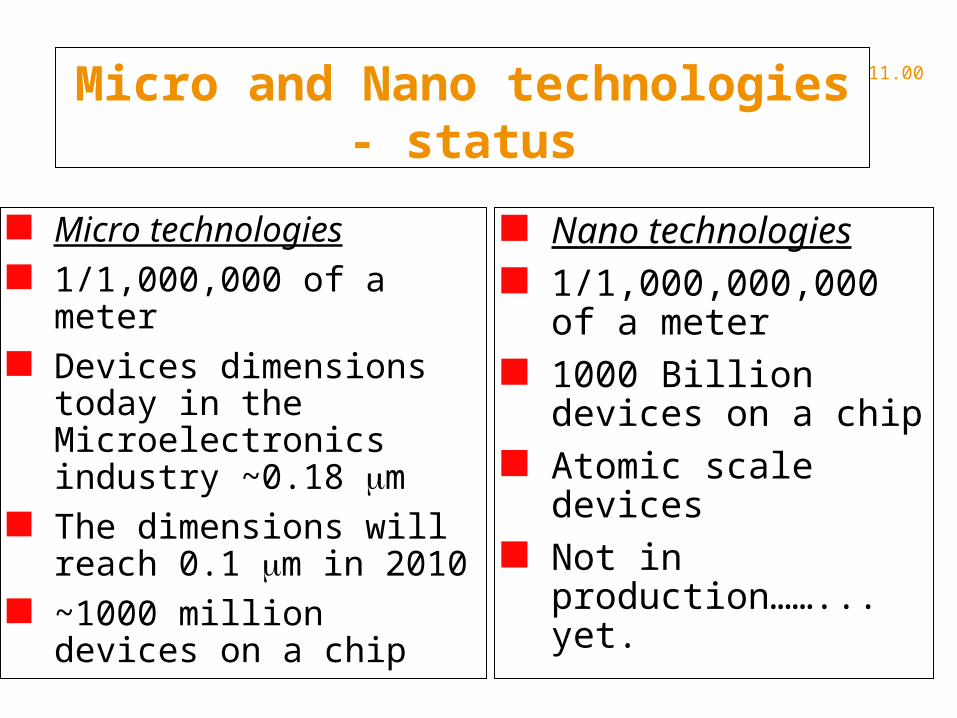
YSD 11.00Micro and Nano technologies - status
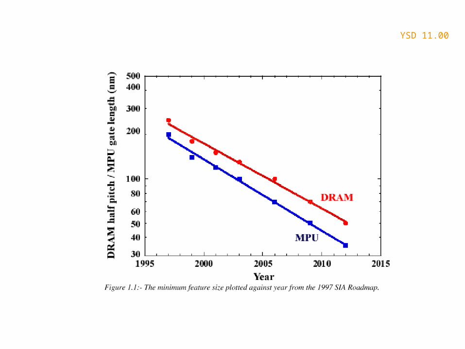
Micro technologies 1/1,000,000 of a meter Devices dimensions
today in the Microelectronics industry ~0.18 m
The dimensions will reach 0.1 m in 2010
~1000 million devices on a chip
Nano technologies 1/1,000,000,000 of a
meter 1000 Billion devices
on a chip Atomic scale devices Not in
production……... yet.
YSD 11.00
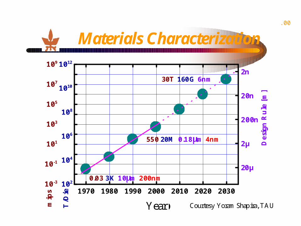
Materials Characterization
1970 1980 1990 2000 2010 2020 203010-3
10-1
101
103
105
107
109
30T 160G 6nm
550 20M 0.18m 4nm
0.03 3K 10m 200nm
mip
s
T/D
ie
20µ
2µ
200n
20n
2n
Des
ign
Rul
e [m
]
102
104
106
108
1010
1012
Year Courtesy Yoram Shapira, TAU
YSD 11.00
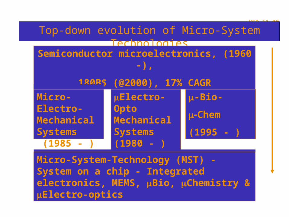
Top-down evolution of Micro-System Technologies
Semiconductor microelectronics, (1960 -),
180B$ (@2000), 17% CAGR
Micro-Electro-Mechanical Systems (1985 - )
Electro-Opto Mechanical Systems (1980 - )
-Bio-
Chem
(1995 - )
Micro-System-Technology (MST) - System on a chip - Integrated electronics, MEMS, Bio, Chemistry & Electro-optics
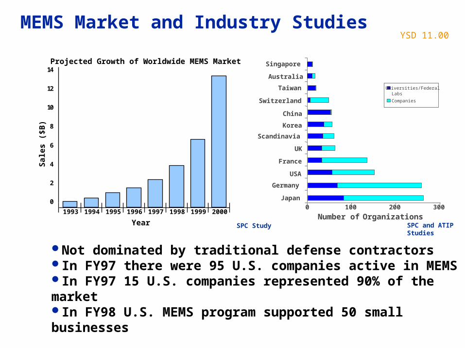
YSD 11.00MEMS Market and Industry Studies
Not dominated by traditional defense contractorsIn FY97 there were 95 U.S. companies active in MEMSIn FY97 15 U.S. companies represented 90% of the market In FY98 U.S. MEMS program supported 50 small businesses
Sa
les
($
B)
SPC Study
0 100 200 300
Germany
Japan
USA
France
UK
Scandinavia
Korea
China
Switzerland
Taiwan
Australia
Singapore
Number of Organizations
Universities/FederalLabs
Companies
SPC and ATIP Studies
Projected Growth of Worldwide MEMS Market
0
2
4
6
8
10
12
14
1993
Year
1994 1995 1996 1997 1998 1999 2000
YSD 11.00
Source: Research & Development (July 1998)
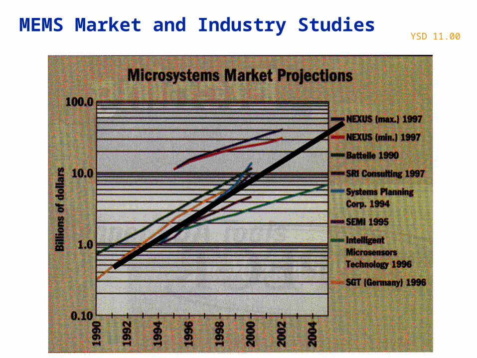
MEMS Market and Industry Studies
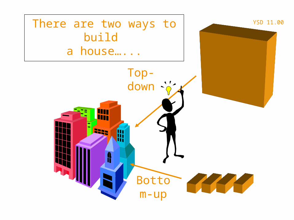
YSD 11.00There are two ways to build a house…...
Top-down
Bottom-up
YSD 11.00
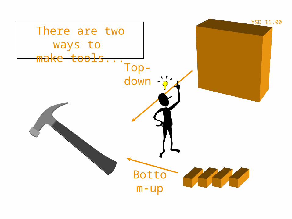
There are two ways to make tools...
Top-down
Bottom-up
YSD 11.00
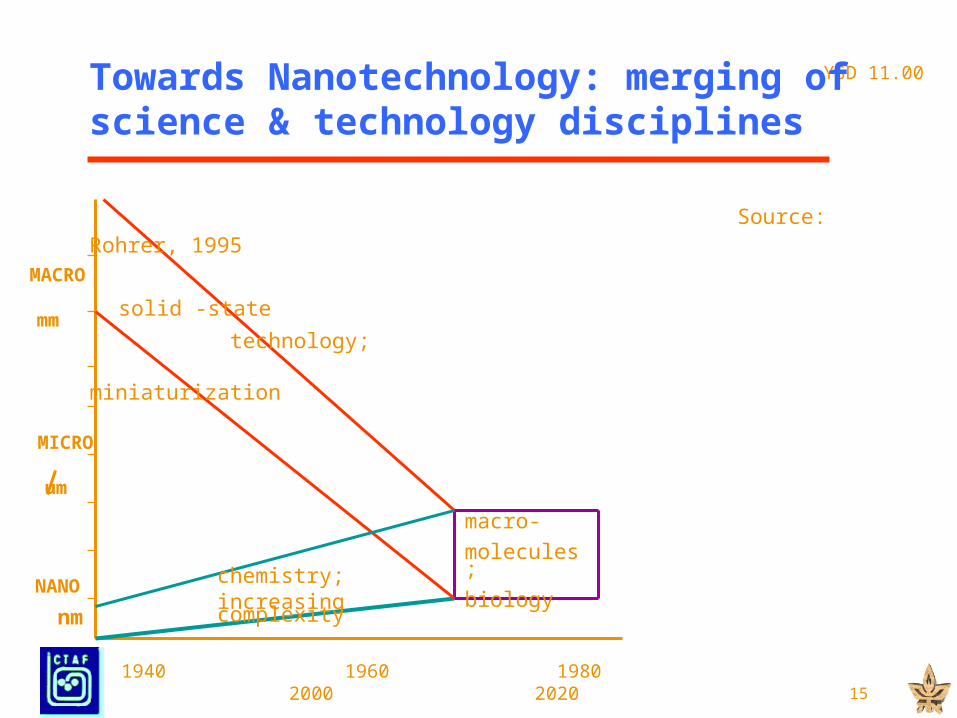
1940 1960 1980 2000 2020
MACRO
mm
MICRO
um
NANO
nm
solid -state
technology;
miniaturization
chemistry;increasing complexity
macro-
molecules;
biology
Towards Nanotechnology: merging of science & technology disciplines
Source: Rohrer, 1995
15
YSD 11.00
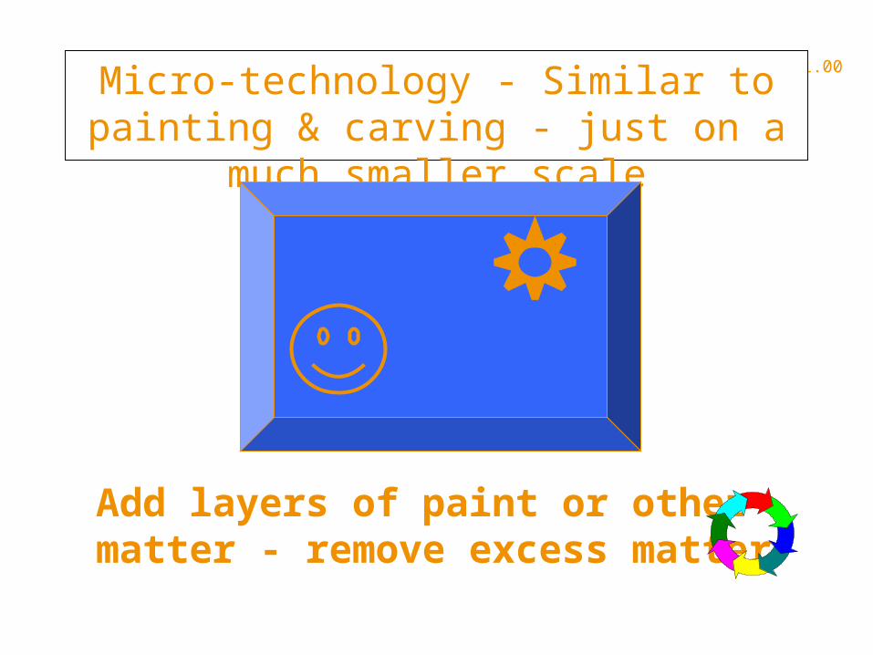
YSD 11.00Micro-technology - Similar to painting &
carving - just on a much smaller scale
Add layers of paint or other matter - remove excess matter
YSD 11.00
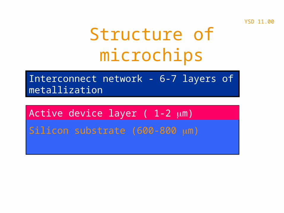
Structure of microchips
Silicon substrate (600-800 m)
Active device layer ( 1-2 m)
Interconnect network - 6-7 layers of metallization
YSD 11.00
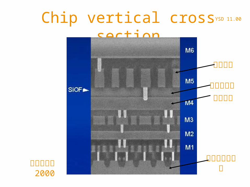
Chip vertical cross section
אינטל 2000
מתכת
מבודד
מתכת
סיליקון
YSD 11.00
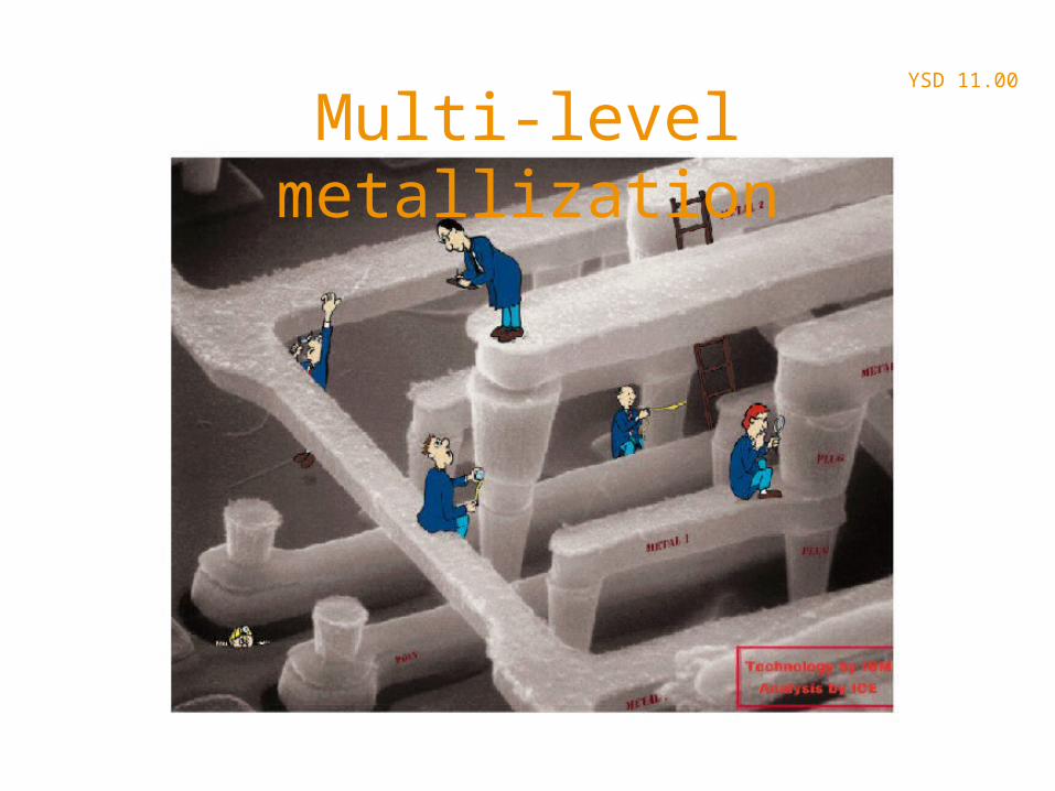
Multi-level metallization
YSD 11.00
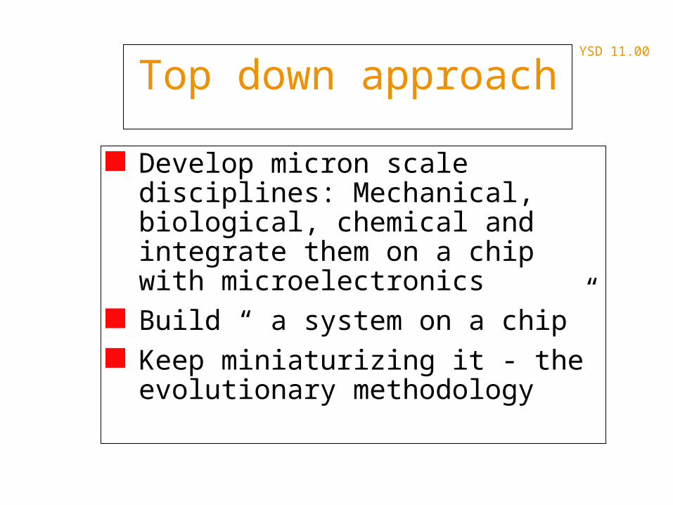
Top down approach
Develop micron scale disciplines: Mechanical, biological, chemical and integrate them on a chip with microelectronics
Build “ a system on a chip” Keep miniaturizing it - the
evolutionary methodology
YSD 11.00
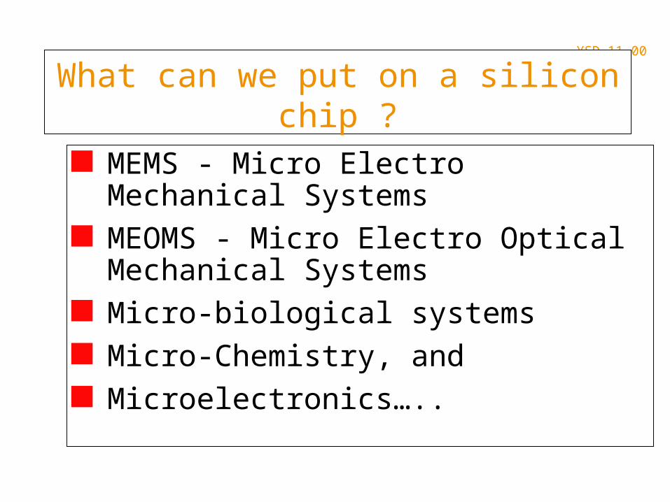
What can we put on a silicon chip ?
MEMS - Micro Electro Mechanical Systems
MEOMS - Micro Electro Optical Mechanical Systems
Micro-biological systems Micro-Chemistry, and Microelectronics…..
YSD 11.00
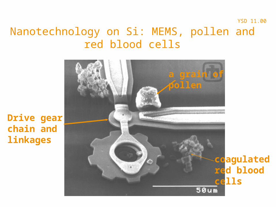
Nanotechnology on Si: MEMS, pollen and red blood cells
Drive gear chain and linkages
a grain of pollen
coagulated red blood cells
YSD 11.00
YSD 11.00
YSD 11.00
מה היתרון של מערכות על שבב ?
ניתן לממש מערכות בחוג סגור על שבב:
בקרה על מערכות אלקטרוניות, חומניות, מכניות, •נוזלים, מגנטים, אופטיות וזרימת מסהעם
שימוש בטכנולוגיות•
MEMS, MEOMS, BIO, CHEMISTRY
מערכות מיקרוסקופיות יכולות ליצור אפקטים הן •ברמה המיקרוסקופית והן ברמה המקרוסקופית.
YSD 11.00(טכמ”מ) טכנולוגיות מערכות ממוזערות
? מהן מערכות ממוזערות
מערכות עם התקנים אלקטרונים, מכניים, כימיים –וביולוגיים בממדים קטנים.
? מה מאפיין מערכות אלו
) System on a chip-SOCמערכת על שבב (–כוללת מספר תת-מערכות ומשלבת מספר פעולות.
למשל ניתן לשלב חישה, חישוב, הפעלה )ACTUATION.תקשורת, ובקרה על אותו שבב ,(
מערכות ממוזערות יכולות לחוש, לחשב ולפעול באופןשישנה את תפישתנו לגבי יכולתנו לקלוט ולשלוט בעולמנו.
Micro Systems Technologies (MST)
YSD 11.00
מדוע לשלב מערכות על אותו שבב ?. שיפור ביצועים - הגדלת מהירות, הורדת הספק )הגדלת 1
זמן שימוש(
. הקטנת נפח, שטח - יותר ניידות, גישה ונוחות.2
בזיווד ואריזת מספר רכיבים ן. הקטנת מחיר - חסכו3ביחד.
יותר . הגדלת אמינות - פחות חיבורים, נפח קטן4
. קלות תכנון - יצירת מערכים גדולים עם אותם 5תאי-יחידה
. הקטנת פרמטרים פרזיטיים - קיבוליות, השראות.6
. חסכון בנפח מגיבים בתהליכים כימים7
YSD 11.00
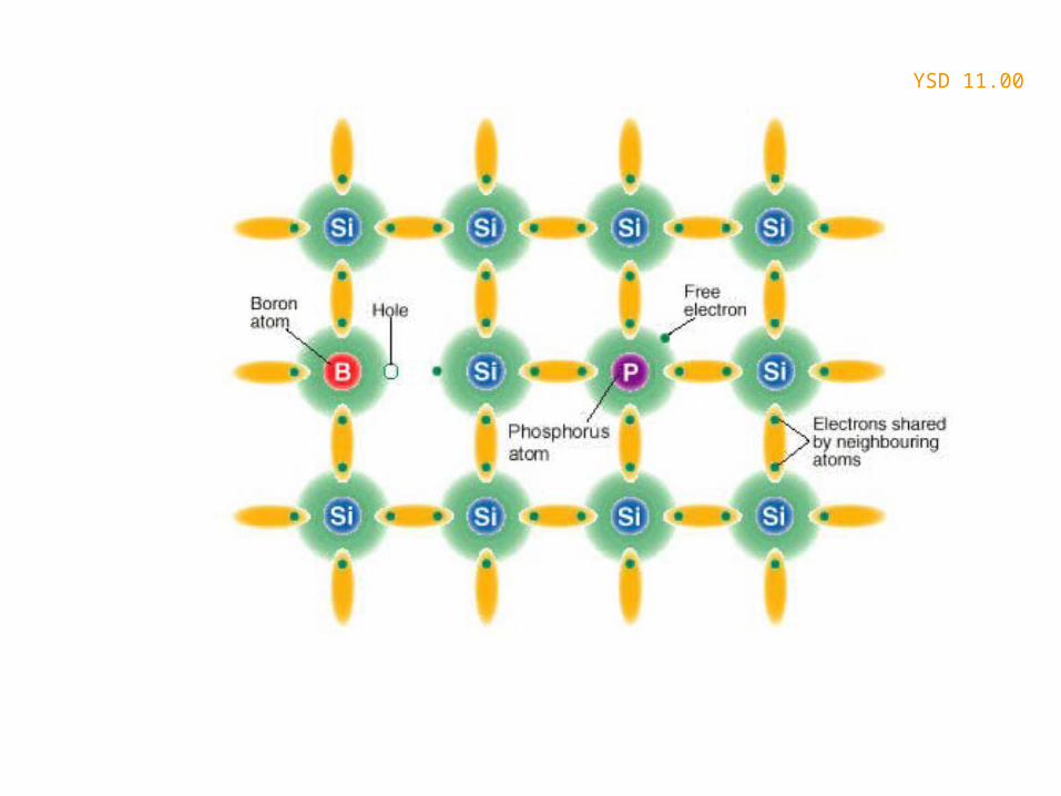
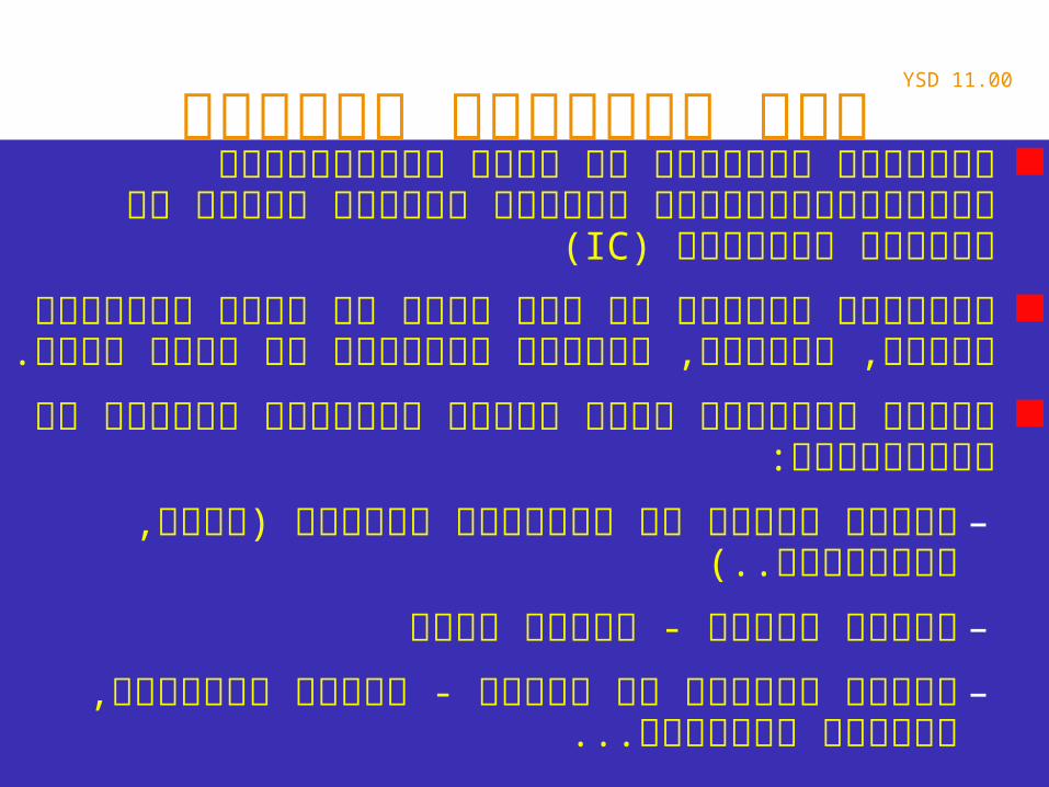
איך מייצרים מערכות ממוזערות ? המערכות מיוצרות על בסיס טכנולוגיות מיקרואלקטרוניקה
)ICקיימות לייצור המוני של מעגלים משולבים (
,המערכות נמצאות על פני השטח של מצעי מוליכים למחצהזכוכית, חומרים אורגנים או בנפח שלהם.
:ייצור הרכיבים נעשה בעזרת תהליכים כימיים או פיזיקליים
הוספת שכבות או אלמנטים בודדים (תאים, מולקולות..)–
הורדת שכבות - איכול חומר–
שינוי תכונות של שכבות - שינוי מוליכות, תכונות –אופטיות...
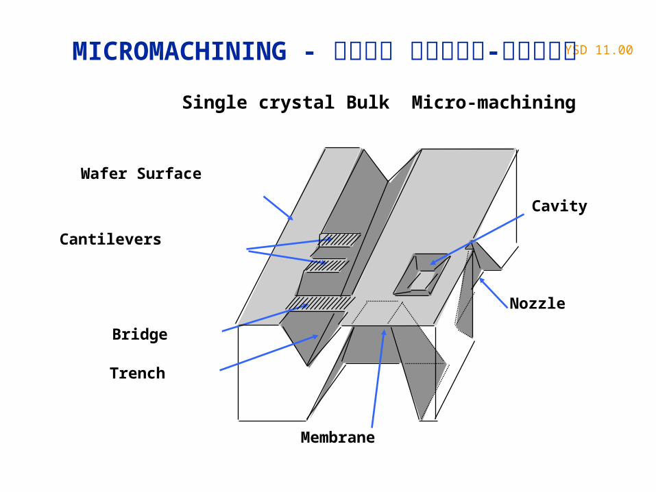
YSD 11.00 - מיקרו-עיבוד חומרMICROMACHINING
Single crystal Bulk Micro-machining
Trench
Bridge
Cantilevers
Wafer Surface
Cavity
Nozzle
Membrane
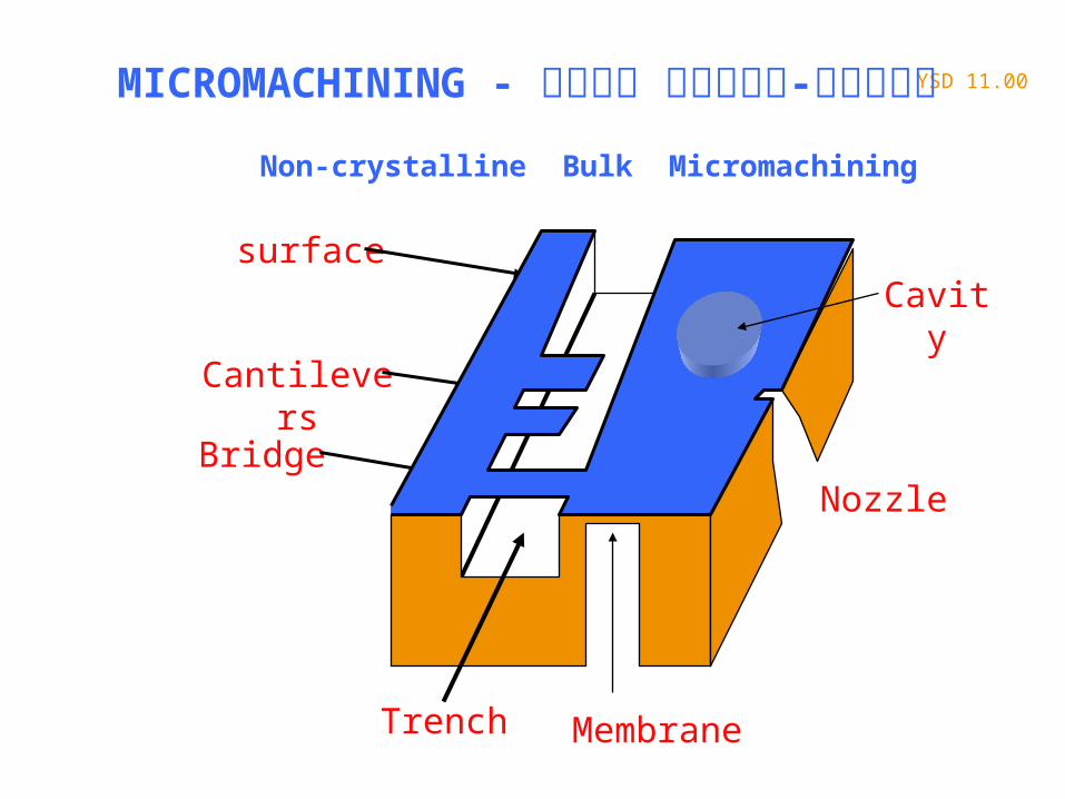
YSD 11.00 - מיקרו-עיבוד חומרMICROMACHINING
Non-crystalline Bulk Micromachining
surface
Cantilevers
Bridge
Trench
Nozzle
Cavity
Membrane
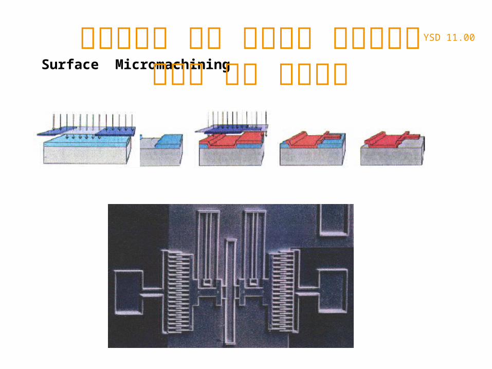
YSD 11.00
Surface Micromachining
עיבוד מכני של שכבות דקות על שבב
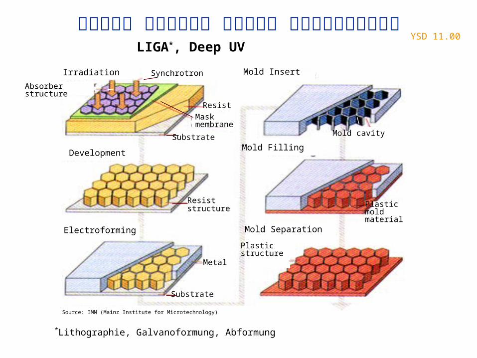
YSD 11.00טכנולוגיות ייצור רכיבים מכנים
LIGA*, Deep UV
*Lithographie, Galvanoformung, Abformung
Irradiation
Development
Electroforming Mold Separation
Synchrotron
Resist
Maskmembrane
Substrate
Resiststructure Plastic
moldmaterial
Plasticstructure
Metal
Substrate
Source: IMM (Mainz Institute for Microtechnology)
Mold cavity
Mold Filling
Absorberstructure
Mold Insert
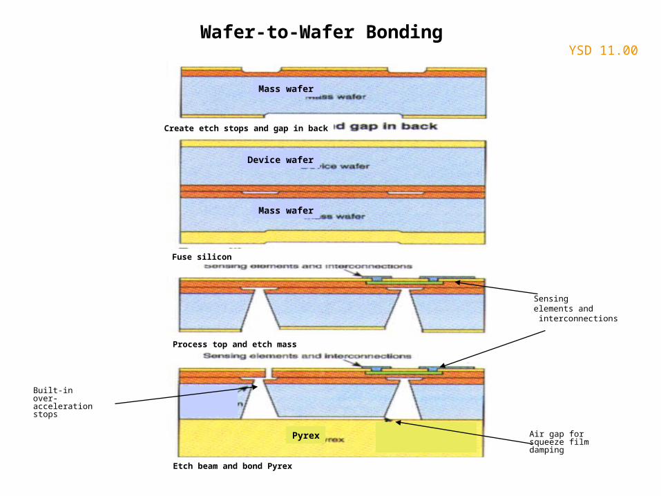
YSD 11.00Wafer-to-Wafer Bonding
Create etch stops and gap in back
Fuse silicon
Process top and etch mass
Etch beam and bond Pyrex
Pyrex Air gap forsqueeze filmdamping
Device wafer
Mass wafer
Built-inover-accelerationstops
Sensingelements and interconnections
Mass wafer
YSD 11.00
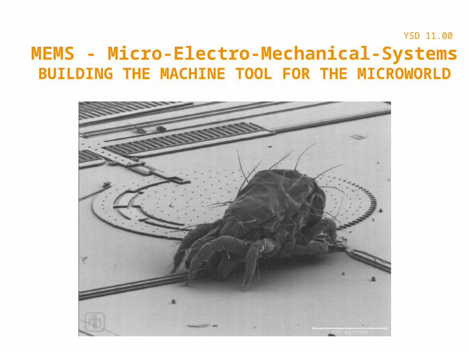
MEMS - Micro-Electro-Mechanical-SystemsBUILDING THE MACHINE TOOL FOR THE MICROWORLD
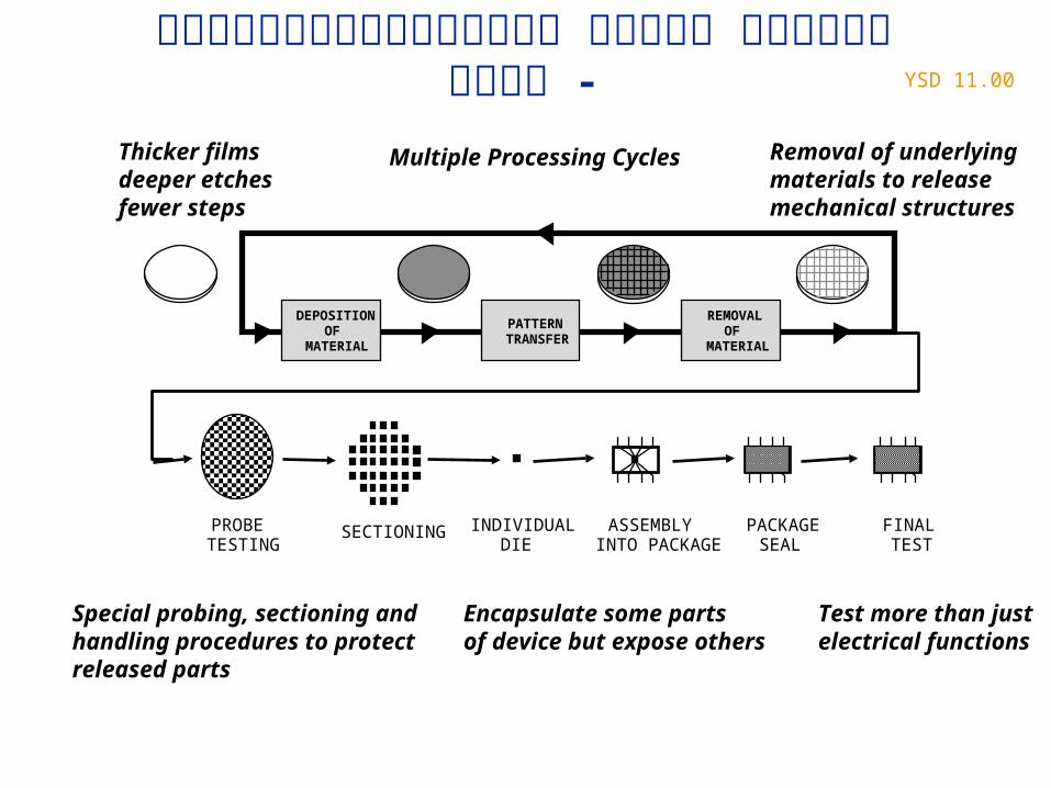
YSD 11.00תהליכי ייצור במיקרואלקטרוניקה - מבוא
Thicker filmsdeeper etchesfewer steps
Removal of underlyingmaterials to releasemechanical structures
Special probing, sectioning and handling procedures to protect released parts
Encapsulate some parts of device but expose others
Test more than just electrical functions
DEPOSITION OF
MATERIAL
PATTERN TRANSFER
REMOVAL OF
MATERIAL
Multiple Processing Cycles
PROBE TESTING
SECTIONING INDIVIDUAL DIE
ASSEMBLY INTO PACKAGE
PACKAGE SEAL
FINAL TEST

YSD 11.00
דוגמה א’ - מערכת קשר ממוזערת
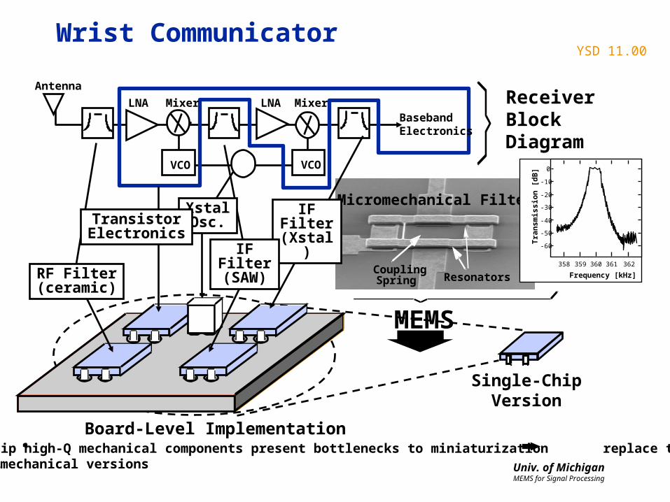
YSD 11.00
Off-chip high-Q mechanical components present bottlenecks to miniaturization replace themwith mechanical versions Univ. of Michigan
MEMS for Signal Processing
Wrist Communicator
Electrode
Anc
Micromechanical Filter
CouplingResonatorsSpring
0
-10
-20
-30
-40
-50
-60
358 359 360 361 362
Frequency [kHz]
Tra
nsm
issi
on
[d
B]
Single-ChipVersion
VCOVCO
XstalOsc.
ReceiverBlockDiagram
BasebandElectronics
Antenna
LNA LNA Mixer Mixer
MEMS
Board-Level Implementation
TransistorElectronics
IF Filter(Xstal)
IF Filter(SAW)
RF Filter(ceramic)
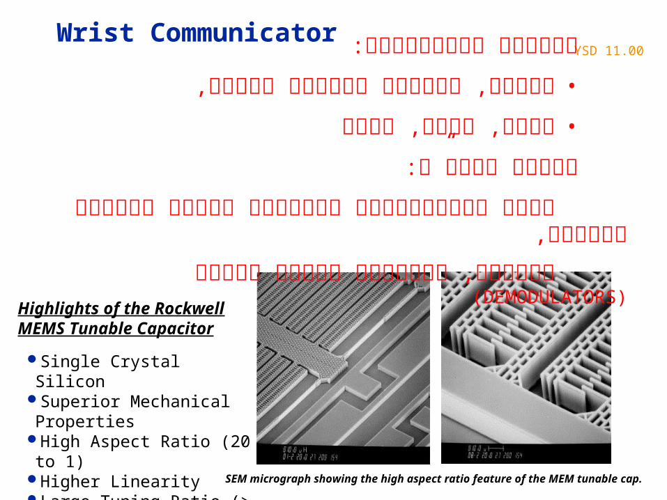
YSD 11.00Wrist Communicator
SEM micrograph showing the high aspect ratio feature of the MEM tunable cap.
Single Crystal SiliconSuperior Mechanical PropertiesHigh Aspect Ratio (20 to 1)Higher LinearityLarge Tuning Ratio (> 6.5 to 1)
Highlights of the Rockwell MEMS Tunable Capacitor
אתגרים טכנולוגים:
אנטנה, מעגלים לברירת תדרים,•
גודל, משקל, הספק•
פתרון בטכמ”מ:
החלף אלקטרוניקה ברכיבים מכנים למימוש מסננים,
)DEMODULATORS(מתנדים, מאפננים וממצי אפנון
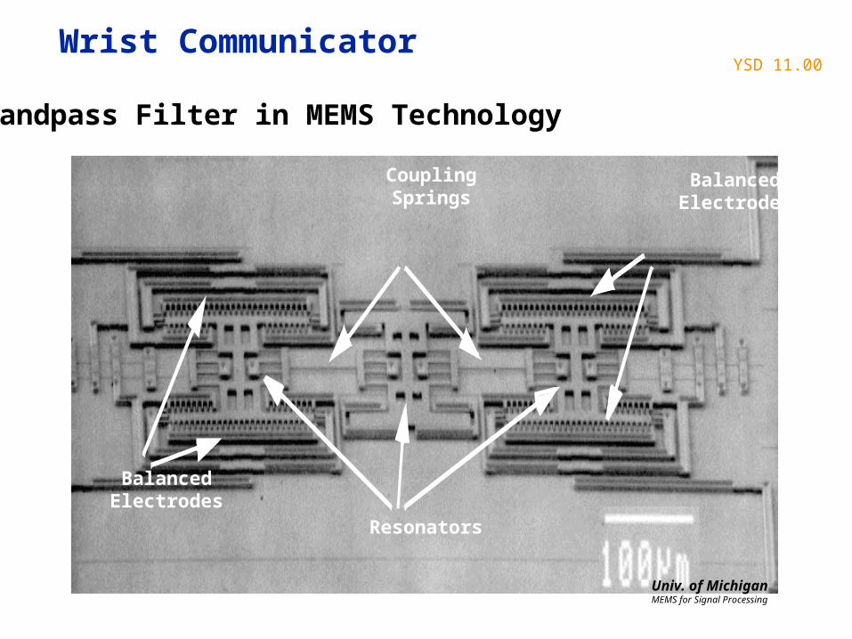
YSD 11.00Wrist Communicator
BalancedElectrodes
CouplingSprings
Resonators
BalancedElectrodes
Sixth-Order Bandpass Filter in MEMS Technology (200 x 700 m)
Univ. of MichiganMEMS for Signal Processing
YSD 11.00
דוגמה ב’ - חיישן משולב
YSD 11.00
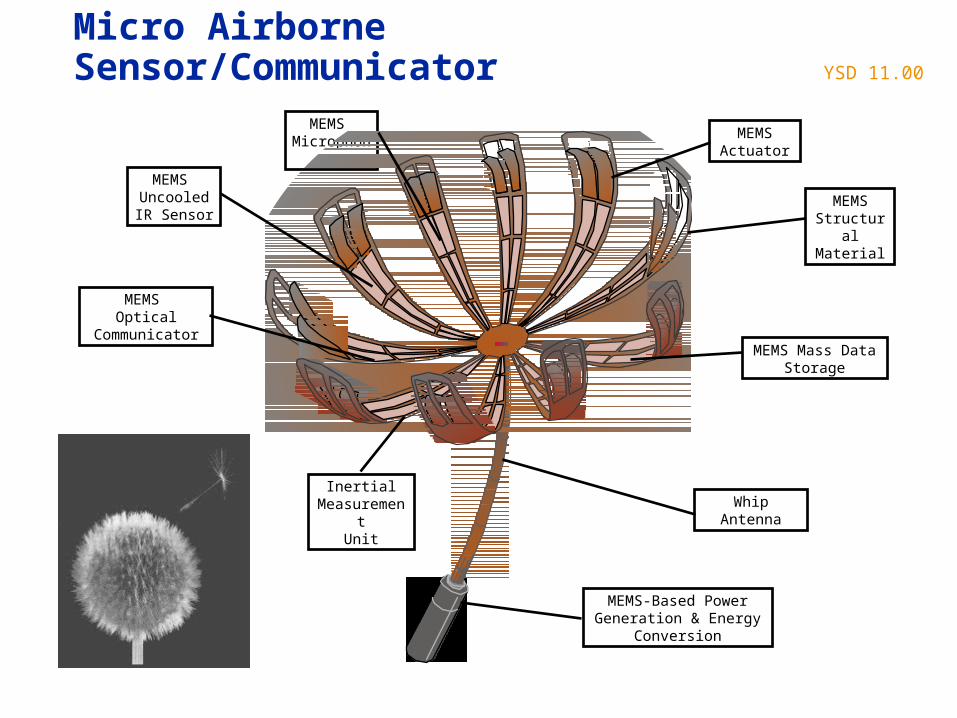
Micro Airborne Sensor/Communicator
MEMS-Based Power Generation & Energy
Conversion
MEMSActuator
Inertial Measurement
UnitWhip
Antenna
MEMS Mass Data Storage
MEMS Microphone
MEMS UncooledIR Sensor
MEMS Optical
Communicator
a
MEMSStructural Material
YSD 11.00
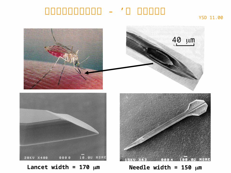
40 m
Lancet width = 170 m Needle width = 150 m
דוגמה ג’ - מיקרומחטים
YSD 11.00ננוטכנולוגיות - השלב הבא...
שילוב בין טכנולוגיות מיקרו לננו - אפשרי כיום•
טכנולוגיות ננו מתקדמות - עדיין לא קיימות•
טכנולוגיות ננו מתקדמות - עדיין יצטרכו ממשק•) INTERFACE ,לעולם החיצון, לאלקטרוניקה (
אופטיקה , מכניקה. קרוב לוודאי שהממשק יהיה בטכנולוגיות מזעור הדומות לטכנולוגיות
מיקרואלקטרוניקה ומיקרו-אלקטרומכניקה כיום.
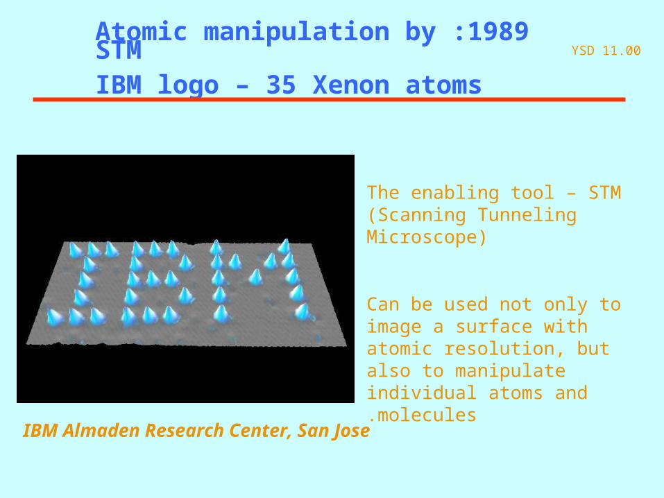
YSD 11.001989 :Atomic manipulation by STM
IBM logo – 35 Xenon atoms
IBM Almaden Research Center, San Jose
The enabling tool – STM (Scanning Tunneling Microscope)
Can be used not only to image a surface with atomic resolution, but also to manipulate individual atoms and molecules.
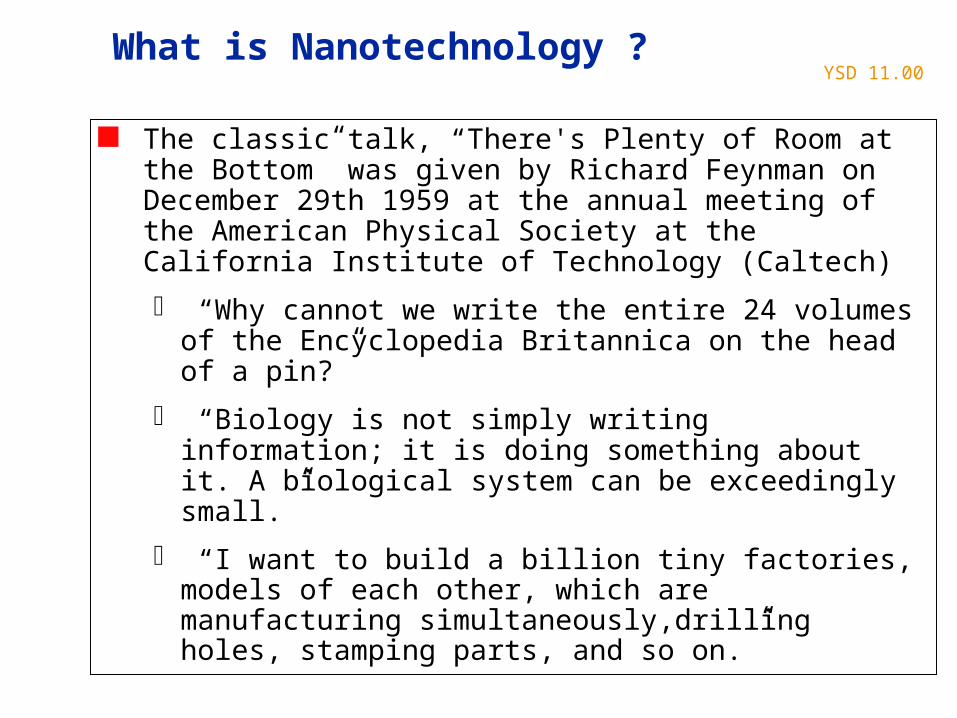
YSD 11.00What is Nanotechnology ?
The classic talk, “There's Plenty of Room at the Bottom” was given by Richard Feynman on December 29th 1959 at the annual meeting of the American Physical Society at the California Institute of Technology (Caltech)
“Why cannot we write the entire 24 volumes of the Encyclopedia Britannica on the head of a pin?”
“Biology is not simply writing information; it is doing something about it. A biological system can be exceedingly small.”
“I want to build a billion tiny factories, models of each other, which are manufacturing simultaneously,drilling holes, stamping parts, and so on.”
YSD 11.00
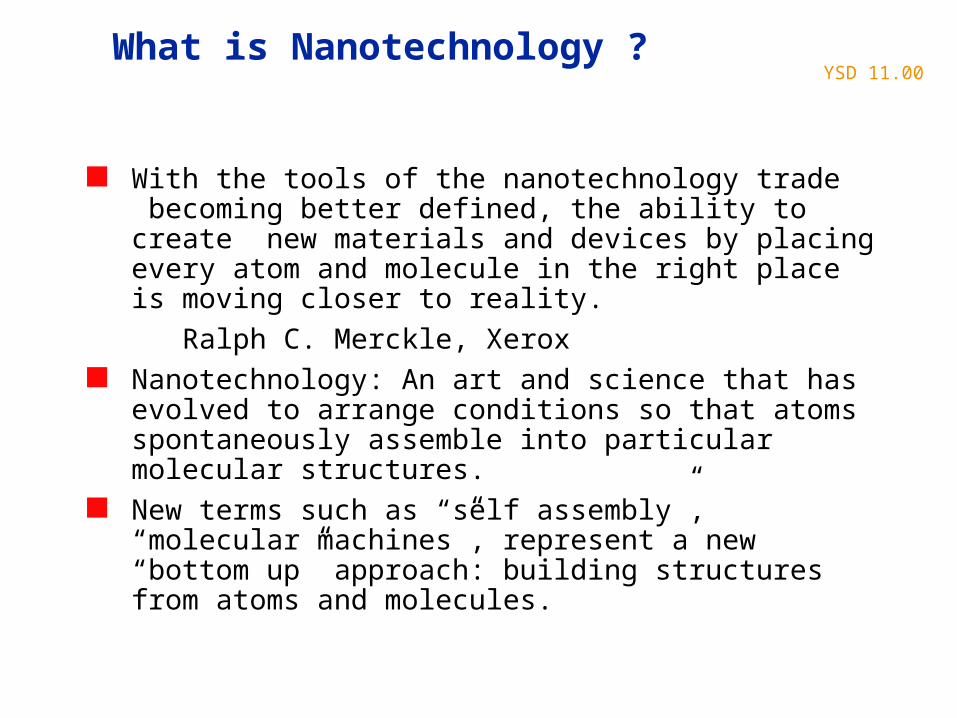
With the tools of the nanotechnology trade becoming better defined, the ability to create new materials and devices by placing every atom and molecule in the right place is moving closer to reality.
Ralph C. Merckle, Xerox
Nanotechnology: An art and science that has evolved to arrange conditions so that atoms spontaneously assemble into particular molecular structures.
New terms such as “self assembly”, “molecular machines”, represent a new “bottom up” approach: building structures from atoms and molecules.
What is Nanotechnology ?
YSD 11.00
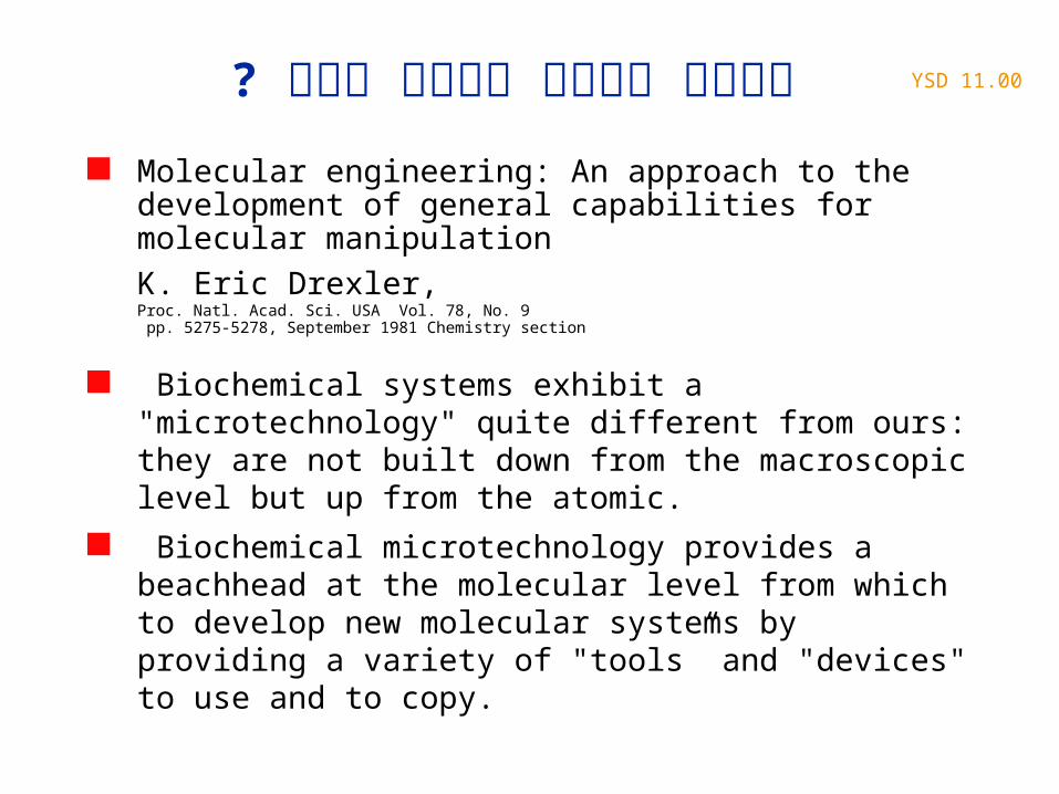
Molecular engineering: An approach to the development of general capabilities for molecular manipulation
K. Eric Drexler, Proc. Natl. Acad. Sci. USA Vol. 78, No. 9 pp. 5275-5278, September 1981 Chemistry
section
Biochemical systems exhibit a "microtechnology" quite different from ours: they are not built down from the macroscopic level but up from the atomic.
Biochemical microtechnology provides a beachhead at the molecular level from which to develop new molecular systems by providing a variety of "tools” and "devices" to use and to copy.
כיצד לממש מבני ננו ?
YSD 11.00
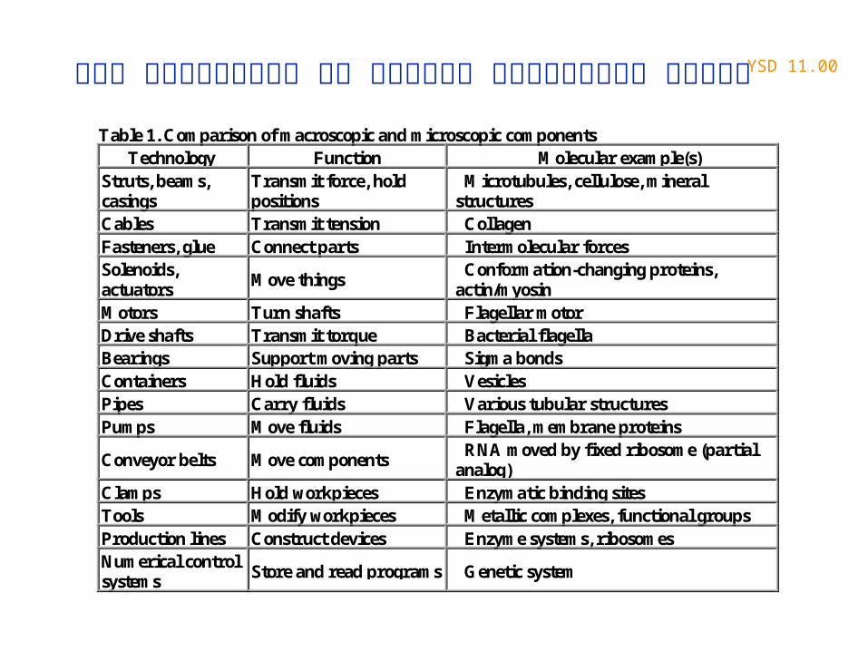
Table 1. Comparison of macroscopic and microscopic componentsTechnology Function Molecular example(s)
Struts, beams,casings
Transmit force, holdpositions
Microtubules, cellulose, mineralstructures
Cables Transmit tension CollagenFasteners, glue Connect parts Intermolecular forcesSolenoids,actuators
Move thingsConformation-changing proteins,
actin/myosinMotors Turn shafts Flagellar motorDrive shafts Transmit torque Bacterial flagellaBearings Support moving parts Sigma bondsContainers Hold fluids VesiclesPipes Carry fluids Various tubular structuresPumps Move fluids Flagella, membrane proteins
Conveyor belts Move componentsRNA moved by fixed ribosome (partial
analog)Clamps Hold workpieces Enzymatic binding sitesTools Modify workpieces Metallic complexes, functional groupsProduction lines Construct devices Enzyme systems, ribosomesNumerical controlsystems
Store and read programs Genetic system
דוגמה לפוטנציאל העתידי של טכנולגיות ננו
YSD 11.00
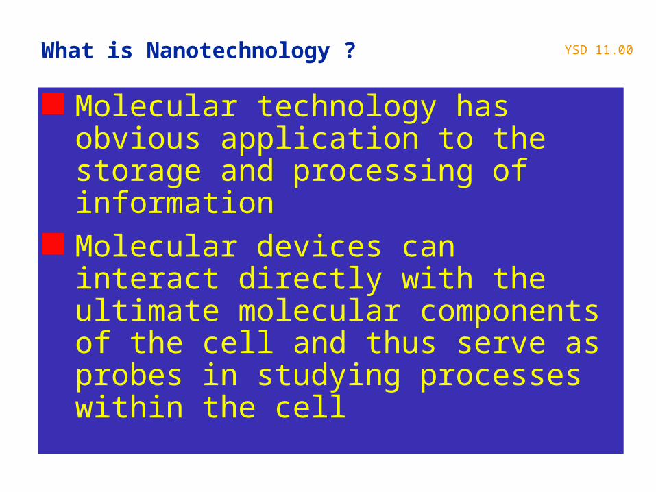
Molecular technology has obvious application to the storage and processing of information
Molecular devices can interact directly with the ultimate molecular components of the cell and thus serve as probes in studying processes within the cell
What is Nanotechnology ?
YSD 11.00
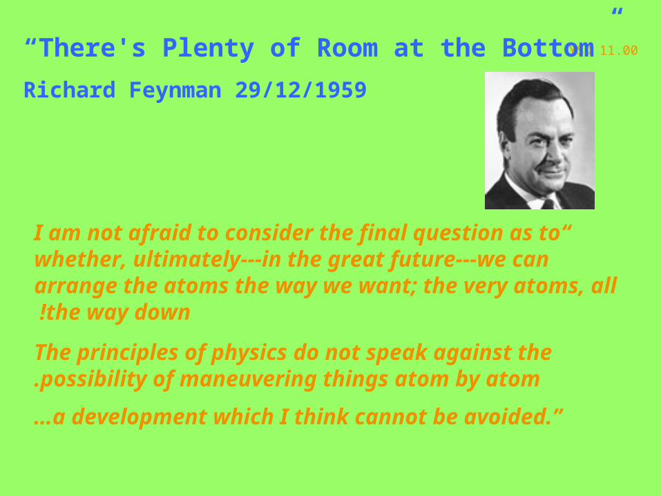
“I am not afraid to consider the final question as to whether, ultimately---in the great future---we can arrange the atoms the
way we want; the very atoms, all the way down !
The principles of physics do not speak against the possibility of maneuvering things atom by atom.
…a development which I think cannot be avoided.”
“There's Plenty of Room at the Bottom”
Richard Feynman 29/12/1959
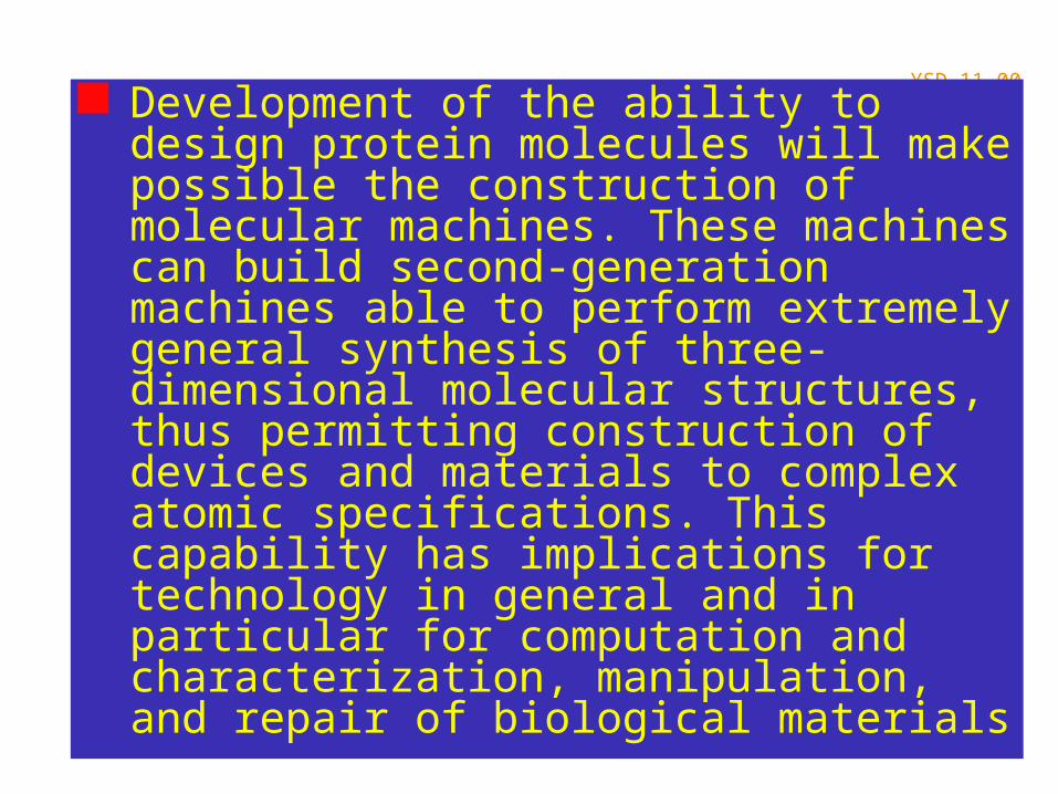
YSD 11.00 Development of the ability to design protein molecules will make possible the construction of molecular machines. These machines can build second-generation machines able to perform extremely general synthesis of three-dimensional molecular structures, thus permitting construction of devices and materials to complex atomic specifications. This capability has implications for technology in general and in particular for computation and characterization, manipulation, and repair of biological materials
YSD 11.00What is Nanotechnology ?
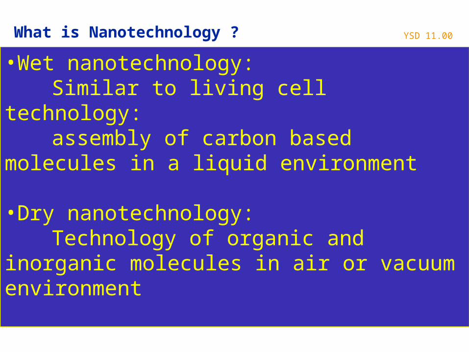
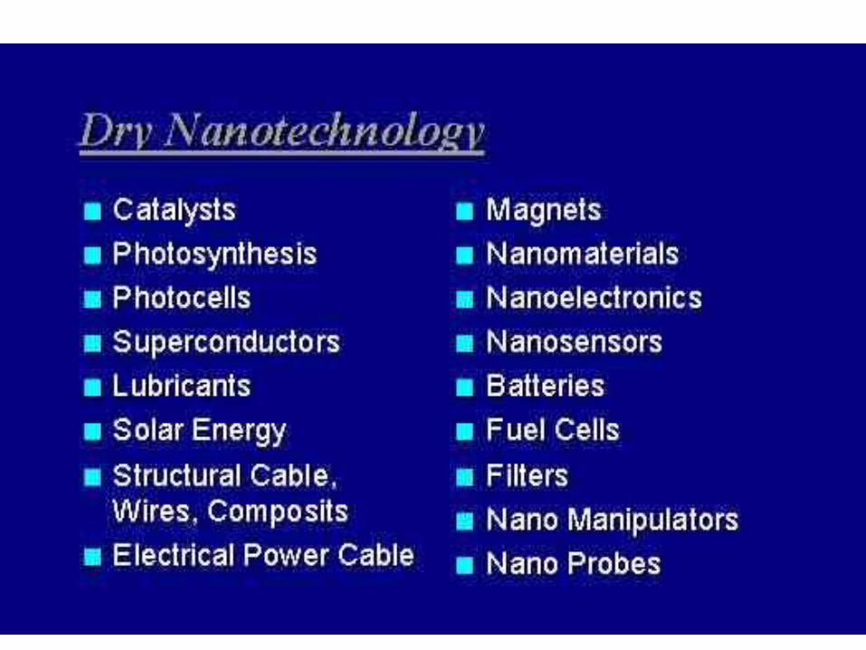
•Wet nanotechnology: Similar to living cell technology: assembly of carbon based molecules in a liquid
environment
•Dry nanotechnology: Technology of organic and inorganic molecules
in air or vacuum environment
YSD 11.00
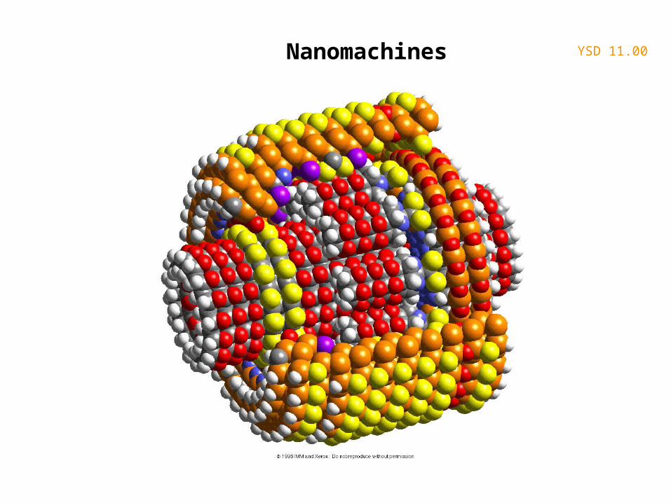
YSD 11.00Nanomachines
YSD 11.00
Large scale industrial nanotechnology
Develop new techniques to produce food, medicine, etc.
Build machines, materials, and devices with the ultimate finesse that life has always used: atom by atom, on the same nanometer scale as the machinery in living cells
Energy production. Replace / complement microelectronics as
leading enabling technology
YSD 11.00
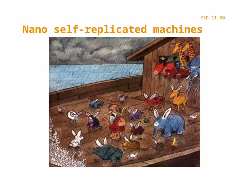
Nano self-replicated machines