Embed Size (px)
Citation preview
1
Performed by: Roman ShterenzonEvgeny Televitsky
Instructor: Erez Sabbag
Cooperated with:
High speed digital systems laboratoryהמעבדה למערכות ספרתיות מהירות
הטכניון - מכון טכנולוגי לישראל
הפקולטה להנדסת חשמל
Technion - Israel institute of technologydepartment of Electrical Engineering
דו”ח סיכום פרויקט )חלק א’/סופי(Subject:
Dual DSP LoCo board
סמסטר )חורף/קיץ( שנה
2
AbstractHigh speed digital systems laboratoryהמעבדה למערכות ספרתיות מהירות
The goal of this project is to create a prototype board for the future satellite use. It will be a PCI factor board built for examining the algorithms and debugging them. This board will consist of two Texas Instruments DSPs and several supporting components.
The second generation of the board will eventually utilize some image compression algorithms, which should be developed by the signal-processing laboratory. This board should be a fast board that could be used to test signal-processing algorithms.
3
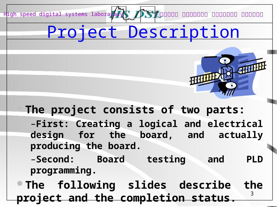
The project consists of two parts:–First: Creating a logical and electrical design for the board, and actually producing the board.–Second: Board testing and PLD programming.
The following slides describe the project and the completion status.
High speed digital systems laboratoryהמעבדה למערכות ספרתיות מהירות
Project Description
4
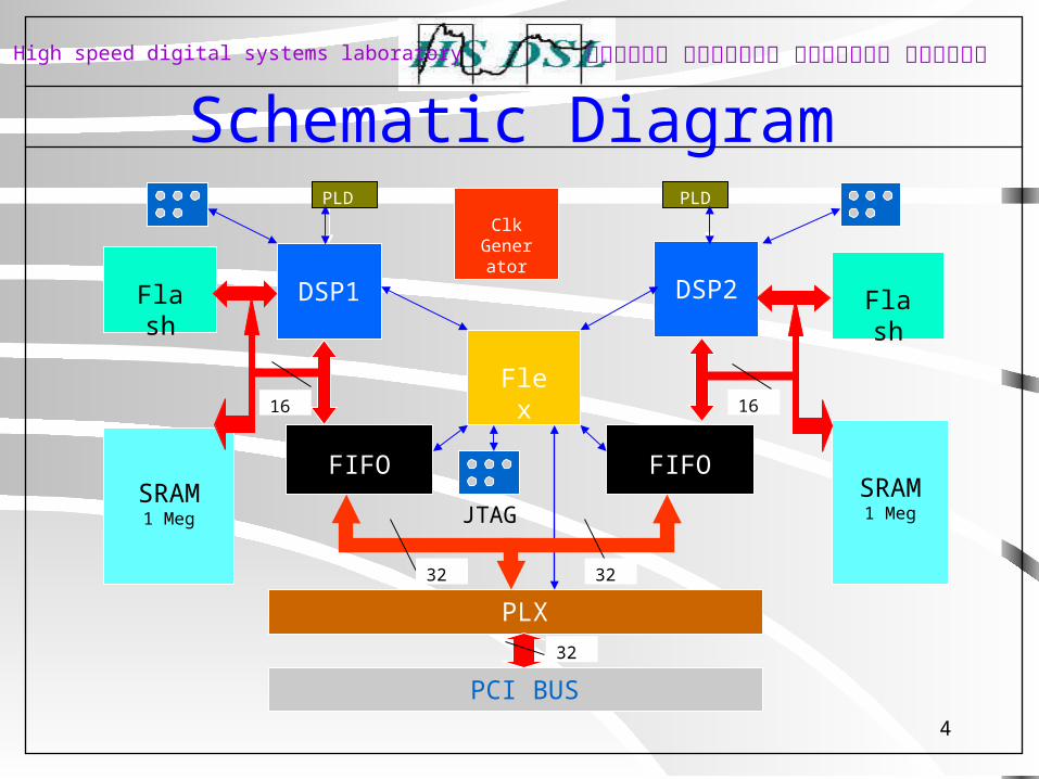
Schematic DiagramHigh speed digital systems laboratoryהמעבדה למערכות ספרתיות מהירות
DSP1 DSP2
SRAM1 Meg
SRAM1 Meg
Flash Flash
ClkGenerat
or
Flex
PLX
FIFO FIFO
PCI BUS
JTAG
PLD PLD
32
3232
16 16
5
Parts DescriptionHigh speed digital systems laboratoryהמעבדה למערכות ספרתיות מהירות
The board will consist of:
• Two Texas Instruments’ DSPs )CPUs(
• Two SRAMs )Temporary and miscellaneous storage(
• Two FlashROMs )Boot code(
• Two Altera MAX 3000A )Simple combinatory logic(
• Two FIFOs
• One PLX PCI chip )PCI interface(
• One Altera Flex chip )The master controller(
• Clock and clock distribution
• Power sources
• Some RCL parts
6
System descriptionHigh speed digital systems laboratoryהמעבדה למערכות ספרתיות מהירות
•Our board will consist of two DSPs and their supporting logic.
•PLX role.
•FIFO role.
•DSP role.
•Peripheral role )FlashRom, SRAM(.
•Flex role.
•Schematic Diagram
7
Data Flow And ControlHigh speed digital systems laboratoryהמעבדה למערכות ספרתיות מהירות
• The input data transaction: )PCI->PLX->Fifo->DSP(
• The data arrives to the PLX9054 from the PCI bus.
• The address is given in order to define where we want a data to go )FIFO1, FIFO2 or both(.
• From FIFO data goes to DSP.
• FIFO full / FIFO empty treatment
•Schematic Diagram
8
Data Flow And Control )cont.(High speed digital systems laboratoryהמעבדה למערכות ספרתיות מהירות
• The output data transaction: )DSP->FIFO->PLX(
• DSP returns data to FIFO or writes to SRAM.
• FIFO returns the data to PLX.
• PLX returns data to PCI.
• FIFO full / FIFO empty treatment
•Schematic Diagram
9
Reset SequenceHigh speed digital systems laboratoryהמעבדה למערכות ספרתיות מהירות
There are two options for reset:1. Soft reset: Reset from PCI board through PLX to Flex and then distributed to all other parts.2. Hard reset: Reset from board itself to Flex and from Flex to the rest of the board. This reset is created using MAX reset generator.
10
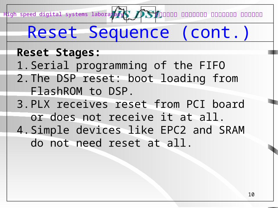
Reset Sequence )cont.(High speed digital systems laboratoryהמעבדה למערכות ספרתיות מהירות
Reset Stages:1. Serial programming of the FIFO2. The DSP reset: boot loading from FlashROM to
DSP.3. PLX receives reset from PCI board or does not
receive it at all. 4. Simple devices like EPC2 and SRAM do not need
reset at all.
11
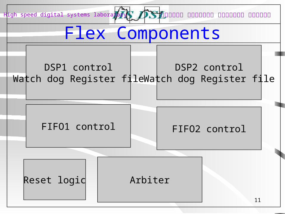
Flex ComponentsHigh speed digital systems laboratoryהמעבדה למערכות ספרתיות מהירות
FIFO1 control
Arbiter
DSP1 controlWatch dog Register file
Reset logic
DSP2 controlWatch dog Register file
FIFO2 control
12
Control UnitsHigh speed digital systems laboratoryהמעבדה למערכות ספרתיות מהירות
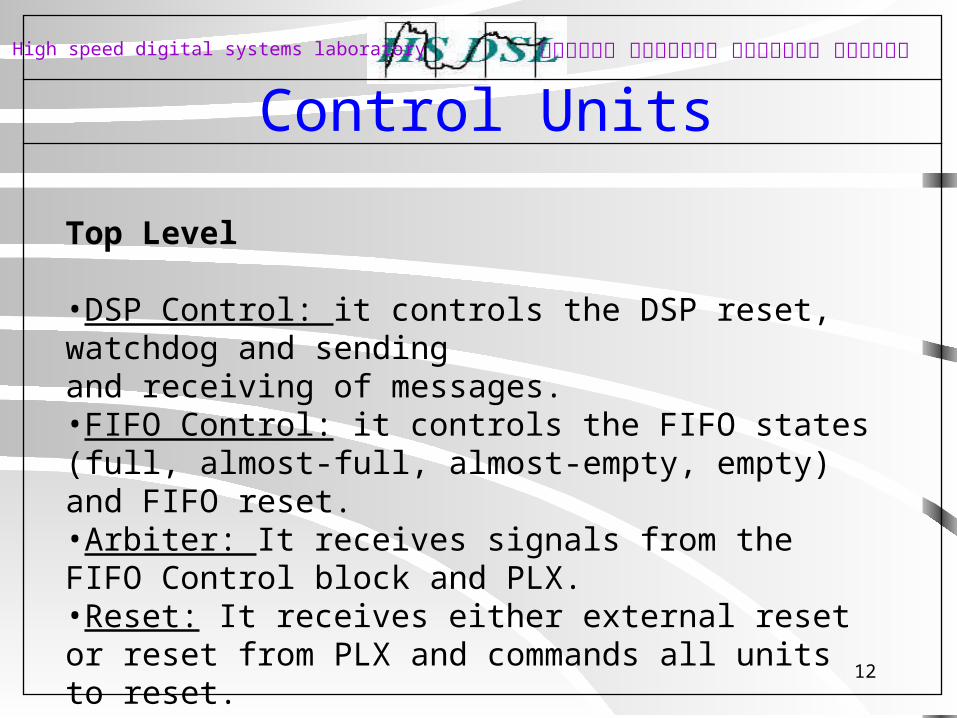
Top Level
•DSP Control: it controls the DSP reset, watchdog and sendingand receiving of messages.•FIFO Control: it controls the FIFO states )full, almost-full, almost-empty, empty( and FIFO reset.•Arbiter: It receives signals from the FIFO Control block and PLX.•Reset: It receives either external reset or reset from PLX and commands all units to reset.
13
VHDL: DSP_ControlHigh speed digital systems laboratoryהמעבדה למערכות ספרתיות מהירות
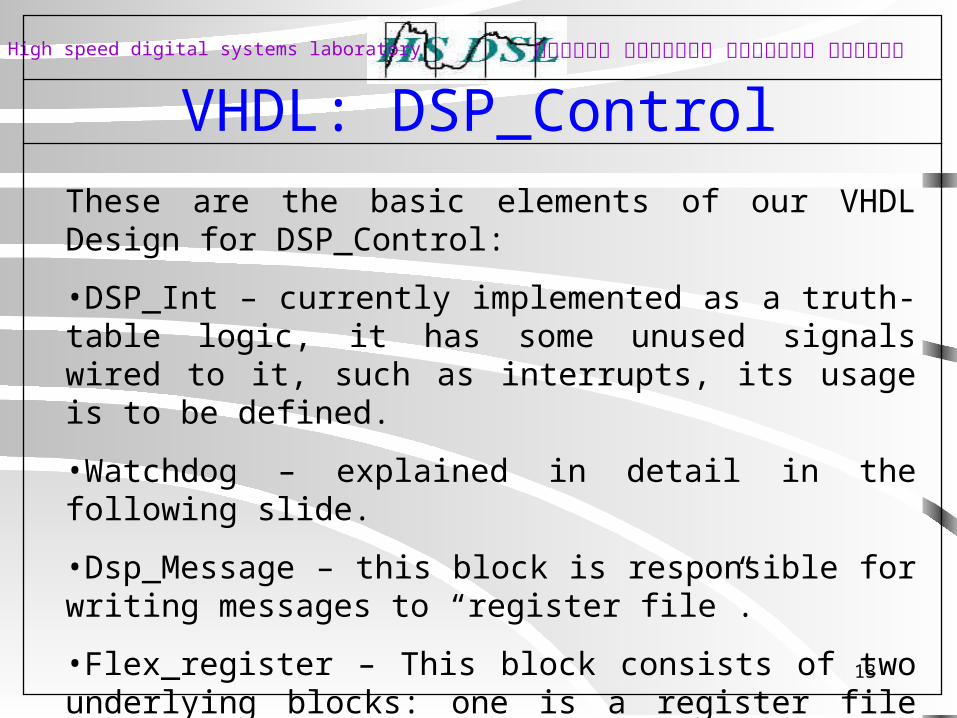
These are the basic elements of our VHDL Design for DSP_Control:
•DSP_Int – currently implemented as a truth-table logic, it has some unused signals wired to it, such as interrupts, its usage is to be defined.
•Watchdog – explained in detail in the following slide.
•Dsp_Message – this block is responsible for writing messages to “register file”.
•Flex_register – This block consists of two underlying blocks: one is a register file and one is an arbiter for the register file.
14
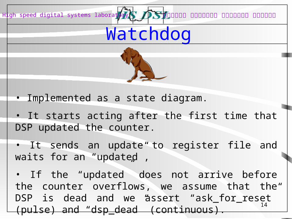
WatchdogHigh speed digital systems laboratoryהמעבדה למערכות ספרתיות מהירות
• Implemented as a state diagram.
• It starts acting after the first time that DSP updated the counter.
• It sends an update to register file and waits for an “updated”,
• If the “updated” does not arrive before the counter overflows, we assume that the DSP is dead and we assert “ask_for_reset” )pulse( and “dsp_dead” )continuous(.
15
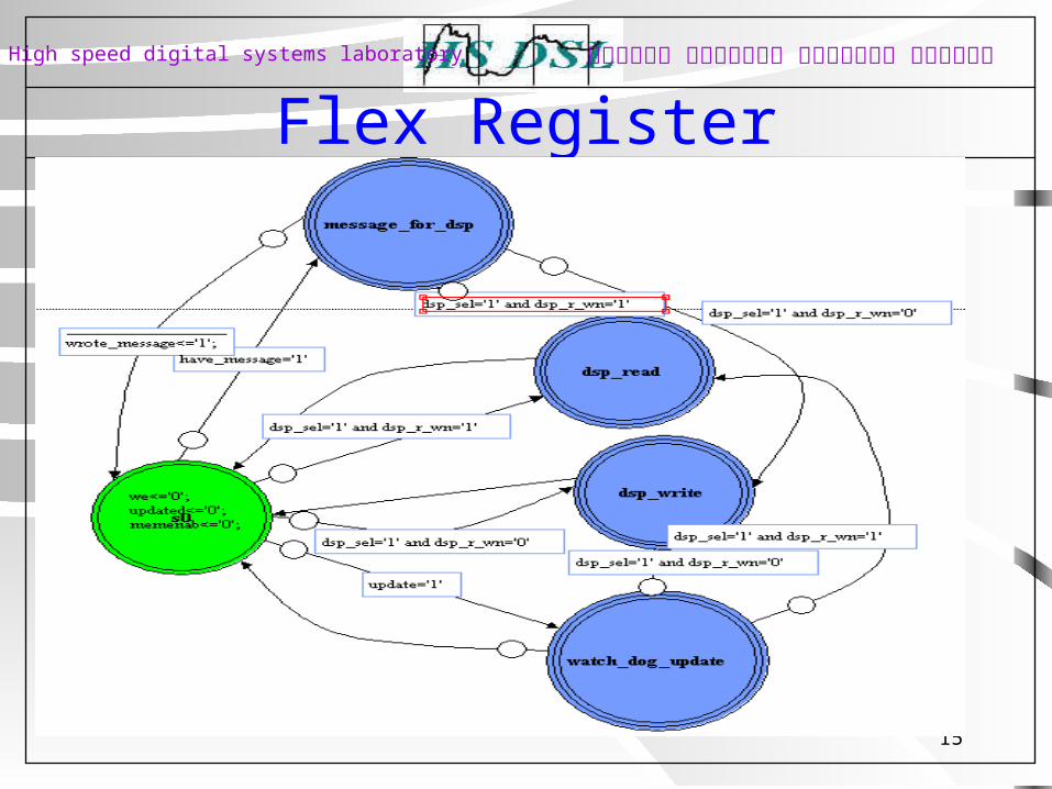
Flex RegisterHigh speed digital systems laboratoryהמעבדה למערכות ספרתיות מהירות
16
Flex Register )cont…(High speed digital systems laboratoryהמעבדה למערכות ספרתיות מהירות
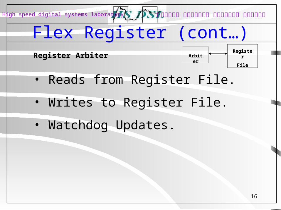
• Reads from Register File.
• Writes to Register File.
• Watchdog Updates.
Register ArbiterRegister
FileArbiter
17
Register fileHigh speed digital systems laboratoryהמעבדה למערכות ספרתיות מהירות
• It is implemented as memory )LPM( with controller.• Entry 0 is watch dog register•All other entries can be accessed by DSP and FLEX for message passing. Or, alternatively, used as GP registers.
18
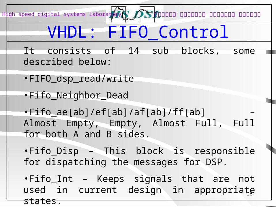
VHDL: FIFO_ControlHigh speed digital systems laboratoryהמעבדה למערכות ספרתיות מהירות
It consists of 14 sub blocks, some described below:
•FIFO_dsp_read/write
•Fifo_Neighbor_Dead
•Fifo_ae[ab]/ef[ab]/af[ab]/ff[ab] – Almost Empty, Empty, Almost Full, Full for both A and B sides.
•Fifo_Disp – This block is responsible for dispatching the messages for DSP.
•Fifo_Int – Keeps signals that are not used in current design in appropriate states.
•Fifo_Reset – Makes a reset to the FIFO. It is also programs them for almost full and almost empty states.
19
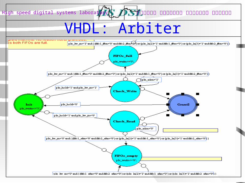
VHDL: ArbiterHigh speed digital systems laboratoryהמעבדה למערכות ספרתיות מהירות
20
VHDL: Arbiter )cont…(High speed digital systems laboratoryהמעבדה למערכות ספרתיות מהירות
• Arbiter is implemented as a FSM.
• Responsible for the bus arbitration and write-target selection.
• Write to first, to second or both FIFOs.
• FIFO is full.
• FIFO is empty.
21
VHDL: ResetHigh speed digital systems laboratoryהמעבדה למערכות ספרתיות מהירות
• Reset is implemented as a state diagram.
• Reset begins from starting state, which called “No_Reset”.
• Then we receive a reset signal we go to the next state and wait for the end of reset pulse.
• FIFOs should be first to wake up and be ready to receive data.
• It will take a long time for DSP to wakeup, as it should initialize PLL.
• Return to the starting state and wait for another reset.
22
DSP to DSPHigh speed digital systems laboratoryהמעבדה למערכות ספרתיות מהירות
DSP may access the other DSP using the following four ways:
1. Serial port 0 access.
2. General-purpose pins. )HPI8(
3. Communicating through register file.
4. Connecting all the way through two FIFOs. Optional. Not implemented.
23
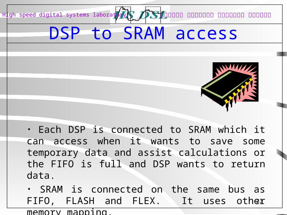
DSP to SRAM accessHigh speed digital systems laboratoryהמעבדה למערכות ספרתיות מהירות
• Each DSP is connected to SRAM which it can access when it wants to save some temporary data and assist calculations or the FIFO is full and DSP wants to return data.• SRAM is connected on the same bus as FIFO, FLASH and FLEX. It uses other memory mapping.
24
Programming & JTAGHigh speed digital systems laboratoryהמעבדה למערכות ספרתיות מהירות
• The Flex is programmed via the DSP’s JTAG interface.• The PLD is programmed via its own interface.• In our device there are five JTAG ports:• We used JTAG port for each device in order to make device programming simple.
25
Sample DSP ProgramHigh speed digital systems laboratoryהמעבדה למערכות ספרתיות מהירות
•We have written a sample DSP program for testing the design.
•The program performs a FIR algorithm on the received data and then sends the data back.
•This loop is continued forever.
•We also included a sample DSP to DSP connection function using the McBSP )serial port( connection method.

26
TestingHigh speed digital systems laboratoryהמעבדה למערכות ספרתיות מהירות
• Electrical probes were added to probe the most crucial electrical signals.• There’re five JTAG sockets, one for each DSP, one for each PLD and one for Flex. It can be used for in depth analysis of the pins and signals.• After the electrical and logical design is verified, a small program described the slide before can be used for testing the design.

27
ConclusionsHigh speed digital systems laboratoryהמעבדה למערכות ספרתיות מהירות
This project can be described as a very interesting and complicated one.The project was both challenging and educative, as it provided different aspects of electrical and computer design such as: Electrical Design Layout considerations VHDL Design VHDL Testing Sample program writing - understanding the DSP programming.
28
ProblemsHigh speed digital systems laboratoryהמעבדה למערכות ספרתיות מהירות
These are some of the problems that we faced during the project: The project requirements weren’t well defined at first, causing several changes in the process; it slowed down the project. As a direct and indirect consequence, some parts were replaced, some added, some removed. Another cause for these changes was unavailability and/or cost of parts. The Orcad schematics tool didn’t contain many of the components. It took too much time to create the layout.
29
Special Thanx
High speed digital systems laboratoryהמעבדה למערכות ספרתיות מהירות
• Erez Sabag
• Eli Shoshan
• Bruria
• DSL lab
• TI, ALTERA, IDT and all other part contributers
30
Q&A
High speed digital systems laboratoryהמעבדה למערכות ספרתיות מהירות