Embed Size (px)
Citation preview

ACCESS IC LAB
Graduate Institute of Electronics Engineering, NTU
102-1 Under-Graduate Project
Synopsys Synthesis Overview
Speaker: MiddleChou
Adviser: Prof. An-Yeu Wu
Date: 2013/12/05

ACCESS IC LAB Graduate Institute of Electronics Engineering, NTU
P. 2
Outline
Introduction
Synopsys Graphical Environment
Setting Design Environment
Setting Design Constraints
Synthesis Report and Analysis
Save Design and Other Issues
Example

ACCESS IC LAB Graduate Institute of Electronics Engineering, NTU
P. 3
What is Synthesis Synthesis = translation + optimization
We will get a gate level circuit with timing information after
Synthesis
ACCESS IC LAB Graduate Institute of Electronics Engineering, NTU
P. 4
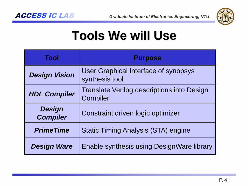
Tools We will Use
Tool Purpose
Design Vision User Graphical Interface of synopsys
synthesis tool
HDL Compiler Translate Verilog descriptions into Design
Compiler
Design
Compiler Constraint driven logic optimizer
PrimeTime Static Timing Analysis (STA) engine
Design Ware Enable synthesis using DesignWare library

ACCESS IC LAB Graduate Institute of Electronics Engineering, NTU
P. 5
Logic Synthesis Overview
no timing info.
timing info.

ACCESS IC LAB Graduate Institute of Electronics Engineering, NTU
P. 6
Design Vision

ACCESS IC LAB Graduate Institute of Electronics Engineering, NTU
P. 7
HDL Compiler
In schematic view, we can see the Verilog file is translated with
a GTECH library (the synopsys default)
GTECH
Library
no timing info

ACCESS IC LAB Graduate Institute of Electronics Engineering, NTU
P. 8
Design Compiler
Design Compiler maps Synopsys design block to gate level
design with a user specified library
Technology
Library
timing info

ACCESS IC LAB Graduate Institute of Electronics Engineering, NTU
P. 9
Synopsys Related Files
Note
These 3 files are always read in the same order.
Any repeated command can override the previous one.
Files Purpose
.cshrc Set path and environment variables and license check
.synopsys_dc.setup
Three distinct files are read and executed when DC is
invoked
1. system-wide (do not modify):
(e.g. $SYNOPSYS/admin/setup/)
2. User‟s home directory (e.g. ~think/)
3. User‟s current working directory (e.g. ~think/dv/)

ACCESS IC LAB Graduate Institute of Electronics Engineering, NTU
P. 10
Synthesis Design Flow Specification
RTL Coding Prepare
Setting Design Environment
Setting Design Constraint
Compile Design
Analysis
Cell
Library
Gate-level Netlist
Develop the HDL design description and simulate the design description to verify that it is correct.
Set up the .synopsys_dc.setup file.
Set the appropriate technology, synthetic, and symbol libraries, target libraries, and link libraries.
Set the necessary compilation options, including options to read in the input files and specify the output formats.
Read the HDL design description.
Define the design.
Set design attributes
Define environmental conditions
Set design rules
Set realistic constraints (timing and area goals)
Determine a compile methodology
ACCESS IC LAB Graduate Institute of Electronics Engineering, NTU
P. 11
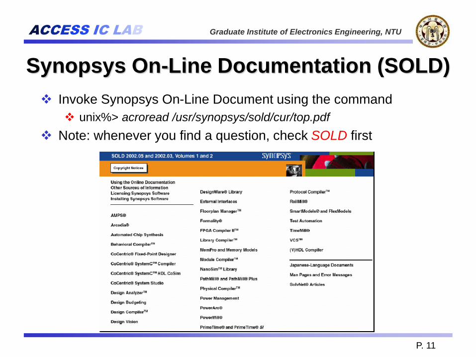
Synopsys On-Line Documentation (SOLD)
Invoke Synopsys On-Line Document using the command
unix%> acroread /usr/synopsys/sold/cur/top.pdf
Note: whenever you find a question, check SOLD first

ACCESS IC LAB
Graduate Institute of Electronics Engineering, NTU
Synopsys Graphical Environment

ACCESS IC LAB Graduate Institute of Electronics Engineering, NTU
P. 13
Invoke Design Vision
Unix%> dv &
dc_shell
command

ACCESS IC LAB Graduate Institute of Electronics Engineering, NTU
P. 14
Read File
Read netlists or other design descriptions into Design Compiler
File/Read
Support many different formats: synopsys internal formats
ddc(binary): .ddc
Verilog: .v
equation: .eqn
state table: .st
VHDL: .vhd
PLA(Berkeley Espresso): .pla
EDIF

ACCESS IC LAB Graduate Institute of Electronics Engineering, NTU
P. 15
Describe the Design Environment
You can use Design Vision to constrain your design

ACCESS IC LAB Graduate Institute of Electronics Engineering, NTU
P. 16
Check Design
Design/Check Design
Execute check_design before you optimize your design
Two types of messages are issued
error
Error: In design „bcd7segs‟, cell „decoder‟ has more pins than it‟s
reference „d1‟ has ports
warnings
Warning: In design „converter‟, port „A‟ is not connected to any nets

ACCESS IC LAB Graduate Institute of Electronics Engineering, NTU
P. 17
Compile the Design
The compile command optimizes and maps the current_design

ACCESS IC LAB Graduate Institute of Electronics Engineering, NTU
P. 18
Report the Design From report and analysis, you can find the set attributes and the
results after optimization
ACCESS IC LAB Graduate Institute of Electronics Engineering, NTU
P. 19
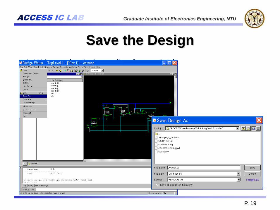
Save the Design
Write out the design netlist after synthesis

ACCESS IC LAB Graduate Institute of Electronics Engineering, NTU
P. 20
Different View - Design View
Hierarchy
Schematic
Symbol
View
Indicator
Current
Design
Indicator

ACCESS IC LAB
Graduate Institute of Electronics Engineering, NTU
Setting Design Environment

ACCESS IC LAB Graduate Institute of Electronics Engineering, NTU
P. 22
What is Design Environment
Describes the real world environment
Beware the defaults are not realistic conditions
Input drive is not infinite
Output loading is usually not zero
Consider process, voltage, temperature (PVT) variation
The operating environment affects the components selected
from target library and timing through your design

ACCESS IC LAB Graduate Institute of Electronics Engineering, NTU
P. 23
Setting Design Environment Setting Operating Environment (a)
Setting Input Driving Strength (b)
Setting Output Loading (c)
Setting Input/Output Delay (d)
Setting Wire Load Model (e)
U1
U2 M1
(a) Set_operating_conditions
(d) set_input_delay
(b) set_driving_cell
(d) set_output_delay
(c) set_load
(e) set_wire_load_model

ACCESS IC LAB Graduate Institute of Electronics Engineering, NTU
P. 24
Setting Design Environment Setting Operating Environment
Setting Input Driving Strength
Setting Output Loading
Setting Input/Output Delay
Setting Wire Load Model

ACCESS IC LAB Graduate Institute of Electronics Engineering, NTU
P. 25
Setting Operating Condition Attributes/Operating Environment/Operating Condition (GUI)
Ex: set_operating_conditions -min_library fsd0a_a_generic_core_1d32vbc -min BCCOM -max_library fsd0a_a_generic_core_1d08vwc -max WCCOM
set_operation_conditions –min_library lib_name –min condition –max_library lib_name –max condition
Maximum => slow ( setup time )
Minimum => fast (hold time)
Ex: set_operating_conditions -min_library fast -min fast -max_library slow -max slow

ACCESS IC LAB Graduate Institute of Electronics Engineering, NTU
P. 26
Setting Design Environment Setting Operating Environment
Setting Input Driving Strength
Setting Output Loading
Setting Input/Output Delay
Setting Wire Load Model

ACCESS IC LAB Graduate Institute of Electronics Engineering, NTU
P. 27
Setting Input Drive Impedance (GUI)
Attribute/Operating Environment/Drive Strength

ACCESS IC LAB Graduate Institute of Electronics Engineering, NTU
P. 28
Setting Input Drive Impedance
Command line or script
Take DFF as example:
set_driving_cell –library max_lib_name –lib_cell DFFX2 –pin{Q} [get_ports your_port]
set_drive [drive_of “max_lib_name/DFFX2/Q”] [get_ports your_port]
or
For Chip design:
set_driving_cell –library IOpad_lib_name –lib_cell PDIDGZ –pin{C} [all_inputs]
or set_drive [drive_of “IOpad_lib_name / PDIDGZ /C”] [all_inputs]

ACCESS IC LAB Graduate Institute of Electronics Engineering, NTU
P. 29
Setting Design Environment Setting Operating Environment
Setting Input Driving Strength
Setting Output Loading
Setting Input/Output Delay
Setting Wire Load Model

ACCESS IC LAB Graduate Institute of Electronics Engineering, NTU
P. 30
Setting Output Loading(GUI)
Attribute/Operating Environment/Load

ACCESS IC LAB Graduate Institute of Electronics Engineering, NTU
P. 31
Setting Output Loading
Command line or script
Take DFF as example:
set_load [load_of “max_lib_name/DFFX1/D”] [get_ports your_port]
For Chip design:
set_load [load_of “IOpad_lib_name / PDT16DGZ /I”] [all_outputs]
load_of “max_lib_name/DFFX1/D”
load_of “IOpad_lib_name / PDT16DGZ /I”
Command line
Command line
script
script

ACCESS IC LAB Graduate Institute of Electronics Engineering, NTU
P. 32
Setting Design Environment Setting Operating Environment
Setting Input Driving Strength
Setting Output Loading
Setting Input/Output Delay
Setting Wire Load Model
ACCESS IC LAB Graduate Institute of Electronics Engineering, NTU
P. 33
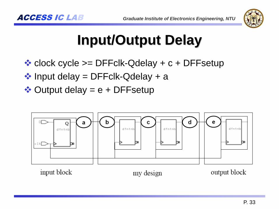
Input/Output Delay
clock cycle >= DFFclk-Qdelay + c + DFFsetup
Input delay = DFFclk-Qdelay + a
Output delay = e + DFFsetup

ACCESS IC LAB Graduate Institute of Electronics Engineering, NTU
P. 34
Setting Input Delay Select input ports
Attributes/Operating Environment/Input Delay
Specify
maximum
input delay
Specify
minimum
input delay

ACCESS IC LAB Graduate Institute of Electronics Engineering, NTU
P. 35
Setting Output Delay Select output ports
Attributes/Operating Environment/Output Delay
Specify
maximum
output delay
Specify
minimum
output delay

ACCESS IC LAB Graduate Institute of Electronics Engineering, NTU
P. 36
Setting Design Environment Setting Operating Environment
Setting Input Driving Strength
Setting Output Loading
Setting Input/Output Delay
Setting Wire Load Model

ACCESS IC LAB Graduate Institute of Electronics Engineering, NTU
P. 37
Setting Wire Load Model
Wire load model estimates wire capacitance based on chip area & cell
fanout
Setting this information during compile in order to model the design
more accurately
Attributes/Operating Environment/Wire Load

ACCESS IC LAB
Graduate Institute of Electronics Engineering, NTU
Setting Design Constraints

ACCESS IC LAB Graduate Institute of Electronics Engineering, NTU
P. 39
Constraints
Constraints are goals that the Design Compiler uses for optimizing a design into target technology library.
Design Rule Constraints : technology-specific restriction; ex. maximum transition, maximum fanout, maximum capacitance.
Optimization Constraints : design goals and requirements; ex. maximum delay, minimum delay, maximum area, maximum power.
During compile, Design Compiler attempts to meet all constraints.

ACCESS IC LAB Graduate Institute of Electronics Engineering, NTU
P. 40
Setting Design Constraints
Optimization Constraints
Basic clock constraints concept
Constraint for Special Circuit
Constraints for Power & Area
Design Rule Constraints
Final check constraints before compile

ACCESS IC LAB Graduate Institute of Electronics Engineering, NTU
P. 41
Define Clock Specification
What should be defined?
Period
Waveform
Uncertainty
Skew
Latency
Source latency (option)
Network latency
Transition
Input transition
Clock transition
All register-to-register path are constrained now
Combinational delay is constraint by
set_max_delay 10 -from all_input -to all_output

ACCESS IC LAB Graduate Institute of Electronics Engineering, NTU
P. 42
Specify Clock Constrains (1/2)
Select clock port
Attributes/Clocks/Specify

ACCESS IC LAB Graduate Institute of Electronics Engineering, NTU
P. 43
Specify Clock Constrains (2/2)
creat_clock : define your clock‟s waveform & respect the set-up time
requirements of all clocked flip-flops
set_fix_hold : respect the hold time requirement of all clocked flip-flops
set_dont_touch_network : do not re-buffer the clock network
create_clock -name "CLK" -period 10 -waveform {0 5} [get_ports CLK ]
set_fix_hold [get_clocks CLK]
set_dont_touch_network [get_clocks CLK]

ACCESS IC LAB Graduate Institute of Electronics Engineering, NTU
P. 44
Setting Area&Power Constraint
Attributes/OptimizationConstraints/Design Constraints
Area Unit :
Equivalent gate count
um x um
Transistors set_max_total_power 0.0uw
set_max_dynamic_power 0.0uw
set_max_leakage_power 0.0uw
set_max_area 0

ACCESS IC LAB Graduate Institute of Electronics Engineering, NTU
P. 45
Setting Design Constraints
Optimization Constraints Basic clock constraints concept
Constraints for Special Circuit
Constraints for Area
Design Rule Constraints
Final check constraints before compile

ACCESS IC LAB Graduate Institute of Electronics Engineering, NTU
P. 46
Design Rule Constraints
Vendors impose design rules that restrict how many cells are
connected to one another based on capacitance, transition ,and
fanout
You may apply more conservative design rules to:
Anticipate the interface environment your block will see
Prevent the design from operating cells close to their limits, where
performance degrades rapidly
DC respects design rules as highest priority of all in the
following order:
set_max_transition
set_max_fanout
set_max_capacitance

ACCESS IC LAB Graduate Institute of Electronics Engineering, NTU
P. 47
Setting Design Constraints
Optimization Constraints
Basic Clock Constraints Concept
Constraints & STA for Special Circuit
Constraints for Area
Design Rule Constraints
Final Check Constraints Before Compile
Check Design
Check Timing
Check Constraints
Save Constraints & Attributes

ACCESS IC LAB Graduate Institute of Electronics Engineering, NTU
P. 48
Check Design
After you set up the deign attributes & design
constraints, we recommend the next step is to check
design
Analysis/Check Design

ACCESS IC LAB Graduate Institute of Electronics Engineering, NTU
P. 49
Setting Design Constraints
Optimization Constraints
Basic Clock Constraints Concept
Constraints & STA for Special Circuit
Constraints for Area
Design Rule Constraints
Final Check Constraints Before Compile
Check Design
Check Timing
Check Constraints
Save Constraints & Attributes

ACCESS IC LAB Graduate Institute of Electronics Engineering, NTU
P. 50
Verify Constraints are Complete in DC
After setting constraints, verify that there are no
remaining unconstrained paths:
Check_timing
Issues warning if unconstrained paths are found
Ex: The following end-points are not constrained for maximum delay.
End point
--------------------------------------
uARM7/uA920/cp1_inst/cp1_rf_inst/reg3_reg0_
.....

ACCESS IC LAB Graduate Institute of Electronics Engineering, NTU
P. 51
Setting Design Constraints
Optimization Constraints
Basic Clock Constraints Concept
Constraints & STA for Special Circuit
Constraints for Area
Design Rule Constraints
Final Check Constraints Before Compile
Check Design
Check Timing
Check Constraints
Save Constraints & Attributes

ACCESS IC LAB Graduate Institute of Electronics Engineering, NTU
P. 52
Check Constraints
Use the following reports to check constraints before compiling
Design/Report XXXX
Report Design
In this report you can check the operating condition and wire load
model
Report Clocks
Notice that all the information about timing is at Timing/Report
XXX

ACCESS IC LAB Graduate Institute of Electronics Engineering, NTU
P. 53
Setting Design Constraints
Optimization Constraints
Basic Clock Constraints Concept
Constraints & STA for Special Circuit
Constraints for Area
Design Rule Constraints
Final Check Constraints Before Compile
Check Design
Check Timing
Check Constraints
Save Constraints & Attributes

ACCESS IC LAB Graduate Institute of Electronics Engineering, NTU
P. 54
Save Constraints & Attributes
Save attributes & constraints setting as the design setup file in
dc_shell command format, use File/Save Info/Design Setup
write_script –output top_setup.tcl
uniquify have to be added by yourself after extract the script
file

ACCESS IC LAB Graduate Institute of Electronics Engineering, NTU
P. 55
Execute Script File
Execute dc_shell command script file, use File/Execute Script

ACCESS IC LAB Graduate Institute of Electronics Engineering, NTU
P. 56
Compile the Design
The compile command optimizes and maps the current_design
Design/Compile design
compile -boundary_optimization -map_effort medium

ACCESS IC LAB
Graduate Institute of Electronics Engineering, NTU
Synthesis Report and Analysis

ACCESS IC LAB Graduate Institute of Electronics Engineering, NTU
P. 58
Report
Design / Report
Timing / Report
ACCESS IC LAB Graduate Institute of Electronics Engineering, NTU
P. 59
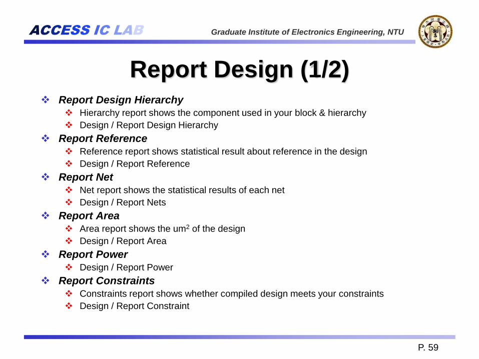
Report Design (1/2) Report Design Hierarchy
Hierarchy report shows the component used in your block & hierarchy
Design / Report Design Hierarchy
Report Reference
Reference report shows statistical result about reference in the design
Design / Report Reference
Report Net
Net report shows the statistical results of each net
Design / Report Nets
Report Area
Area report shows the um2 of the design
Design / Report Area
Report Power
Design / Report Power
Report Constraints
Constraints report shows whether compiled design meets your constraints
Design / Report Constraint

ACCESS IC LAB Graduate Institute of Electronics Engineering, NTU
P. 60
Report Design (2/2)
Extract report data by script file
At the end of script
redirect xxx_area.rpt { report_area }
redirect xxx_power.rpt { report_power }
redirect xxx_hierarchy.rpt { report_hierarchy }
redirect xxx_nets.rpt { report_nets }
redirect xxx_constraints.rpt { report_constraints }
redirect xxx_reference.rpt { report_reference }

ACCESS IC LAB Graduate Institute of Electronics Engineering, NTU
P. 61
Report Timing
Timing report shows maximum or minimum delay path of design,
the default is to display one maximum delay path
redirect xxx_timing.rpt { report_timing }

ACCESS IC LAB Graduate Institute of Electronics Engineering, NTU
P. 62
What is Slack
Slack is the resulting margin between required & actual arrival
time
Positive slack or zero means meet constraints
Negative slack means violate constraints
Setup Time Check (max delay check)
Hold Time Check (min delay check)
Slack_setup = Data Required Time – Data Arrival Time
Slack_hold = Data Arrival Time - Data Required Time

ACCESS IC LAB Graduate Institute of Electronics Engineering, NTU
P. 63
Report Timing Options Timing / Report Timing Path
Fractional part length
ACCESS IC LAB
Graduate Institute of Electronics Engineering, NTU
Save Design and Other Issues

ACCESS IC LAB Graduate Institute of Electronics Engineering, NTU
P. 65
Save Design
Save your design to file before you quit Design Compiler
File/Save saves your design in the ddc format
File/Save As can save your design in other Write formats
Verilog: .v
VHDL: .vhd
EDIF
Synopsys formats
PLA (Berkeley Espresso): .pla
write -hierarchy -format ddc -output xxx.ddc
write -hierarchy -format verilog -output xxx.v

ACCESS IC LAB Graduate Institute of Electronics Engineering, NTU
P. 66
Assign Problem Save your design in verilog format, run Verilog gate-level
simulation, and we will use Verilog In interface to translate it into
OPUS database for place & route
If you can‟t Verilog In, please check assign problem
if there is any assignment problem, choose the block & use the
dc_shell command as follow to fix it
set_fix_multiple_port_nets -all -buffer_constants
set verilogout_no_tri "true"

ACCESS IC LAB Graduate Institute of Electronics Engineering, NTU
P. 67
Change Naming Rule script
set bus_inference_style {%s[%d]}
set bus_naming_style {%s[%d]}
set hdlout_internal_busses true
change_names –hierarchy –rule verilog
define_name_rules name_rule -allowed "A-Z a-z 0-9_“ –max_length 255 –type cell
define_name_rules name_rule -allowed "A-Z a-z 0-9_[]“ –max_length 255 –type net
define_name_rules name_rule –map {{“\\*cell\\*” “cell”}}
define_name_rules name_rule –case_insensitive
change_names –hierarchy –rules name_rule
Write in .synopys_dc.setup

ACCESS IC LAB Graduate Institute of Electronics Engineering, NTU
P. 68
Gate-Level Simulation (Verilog)
Write out gate-level netlist
File/Save As Verilog (for File format)
dc_shell> write -format verilog –hierarchy -output chip.vg
Get SDF
File/Save Info Design timing Select chip.sdf
dc_shell> write_sdf –version 2.1 -context verilog chip.sdf
Modify your testbench file
$sdf_annotate (“the_SDF_file_name”, top_module_instance_name);
Simulation using Verilog-XL
>> ncverilog testbench.v chip.vg –v cell_model.v +access+r
ACCESS IC LAB
Graduate Institute of Electronics Engineering, NTU
Design Example

ACCESS IC LAB Graduate Institute of Electronics Engineering, NTU
P. 70
Synopsys Design Vision (GUI) /
Design Compiler (text mode)
Unix% dv&
Unix% dc_shell

ACCESS IC LAB Graduate Institute of Electronics Engineering, NTU
P. 71
Read Verilog File
read -format verilog {"Lab1_alu.v"}

ACCESS IC LAB Graduate Institute of Electronics Engineering, NTU
P. 72
Schematic View Synopsys Design analyzer will translate verilog code into G-tech
model. Double click the icon “ALU”, and click the right button
then choose Schematic view. We can get the G-tech MAP
ACCESS IC LAB Graduate Institute of Electronics Engineering, NTU
P. 73
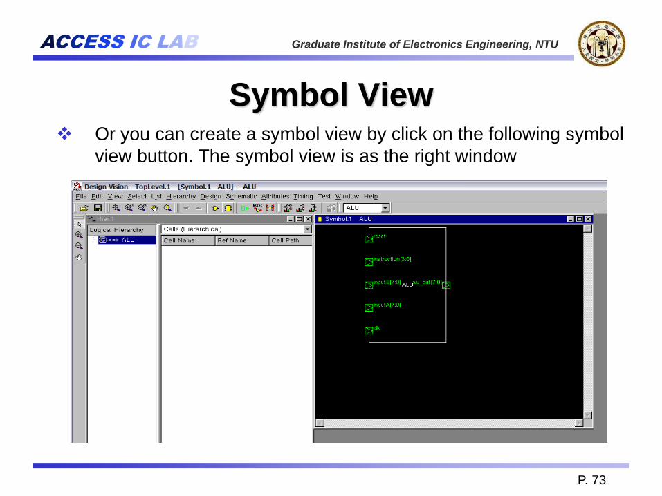
Symbol View Or you can create a symbol view by click on the following symbol
view button. The symbol view is as the right window

ACCESS IC LAB Graduate Institute of Electronics Engineering, NTU
P. 74
Set Clock (1/2)
“Attributes”-“Specify Clock”

ACCESS IC LAB Graduate Institute of Electronics Engineering, NTU
P. 75
Set Clock (2/2) Specify the clock as period 10ns. (100 MHz). Don‟t forget to
select “don’t touch network” and “fix hold”
create_clock -name "clk" -period 10 -waveform {"0" "5"} {"clk"}
set_dont_touch_network find( clock, "clk")
set_fix_hold clk

ACCESS IC LAB Graduate Institute of Electronics Engineering, NTU
P. 76
Operating Condition
set_operating_conditions "typical" -library "typical"

ACCESS IC LAB Graduate Institute of Electronics Engineering, NTU
P. 77
Operating Environment Select “inputA” in the Symbol View and click “Attribute”-
“operating environment”-“input delay”. Set 2.5ns input delay.
set_input_delay -clock clk 2.5 inputA[*]
set_input_delay -clock clk 3.8 inputB[*]
set_input_delay -clock clk 4.5 instruction[*]
set_input_delay -clock clk 5.2 reset
set_output_delay -clock clk 8 alu_out[*]

ACCESS IC LAB Graduate Institute of Electronics Engineering, NTU
P. 78
Area & Fanout & Transition
Click “Attribute”-
”optimization Constraints”-
“Design constraints”. Set
max area is 0. Max fan-out is
8. max transition is 1.
set_max_area 0
set_max_fanout 8 find (design, ALU)
set_max_transition 1 find (design, ALU)

ACCESS IC LAB Graduate Institute of Electronics Engineering, NTU
P. 79
Compile Design Click “Design”-”Compile Design”. Click “OK”, start to optimize
ALU
compile -map_effort medium

ACCESS IC LAB Graduate Institute of Electronics Engineering, NTU
P. 80
Report
report_timing -path full -delay max -max_paths 1 -nworst 1
report_power
report_area -nosplit

ACCESS IC LAB Graduate Institute of Electronics Engineering, NTU
P. 81
Save Files Save gate-level netlist. Select “File”->”Save As”
Save your design. Select “File”-“Save”
Save the timing information. Select “File”-“Save Info”-”Design Timing”, choose sdf format.
Save script file with the constraints you have made. Use “write_script > script_file” command or “File”-”Save Info”-”Design Setup“ button.
Re-run all steps automatically. Use “include script_file” command or “File”-“Execute Script” button.
write -format verilog -hierarchy -output "ALU_s.v" find (design, ALU)
write -format db -hierarchy -output "ALU_s.db" find (design, ALU)
write_sdf ALU_s.sdf

ACCESS IC LAB Graduate Institute of Electronics Engineering, NTU
P. 82
Gate Level Simulation
Before gate level simulation,
$sdf_annotate(“top_design.sdf”, top_design)
must be added after initial in testbench
`timescale 1ns/10ps must be added in the 1st line of
testbench
//RTL simulation
Unix% ncverilog testfixture.v your_file.v +access+r
//gate level simulation
Unix% ncverilog testfixture_vg.v your_file.vg –v
tumc18.v +access+r

ACCESS IC LAB Graduate Institute of Electronics Engineering, NTU
P. 83
View Waveform
Unix% nWave&
Open verilog.fsdb file to see the waveform


![ch-,- (vkWulZ) fganh lsesLVj Ldhe tqykbZ] 2011 ls vkjaHkdu.ac.in/du/uploads/old-ug-courses/2262011_BA_H_Hindi.pdf3 SEMESTER BASED UNDER-GRADUATE HONOURS COURSES Distribution of Marks](https://img.pdfslide.tips/doc/110x75/5f8654deae2a4027355cfe13/ch-vkwulz-fganh-lseslvj-ldhe-tqykbz-2011-ls-3-semester-based-under-graduate.jpg)