Embed Size (px)
Citation preview

Real Analog - Circuits 1Chapter 3: Nodal and Mesh Analysis
© 2012 Digilent, Inc. 1
3. Introduction and Chapter ObjectivesIn Chapters 1 and 2, we introduced several tools used in circuit analysis:
Ohm’s law, Kirchoff’s laws, and circuit reduction
Circuit reduction, it should be noted, is not fundamentally different from direct application of Ohm’s andKirchoff’s laws – it is simply a convenient re-statement of these laws for specific combinations of circuit elements.
In Chapter 1, we saw that direct application of Ohm’s law and Kirchoff’s laws to a specific circuit using theexhaustive method often results in a large number of unknowns – even if the circuit is relatively simple. Acorrespondingly large number of equations must be solved to determine these unknowns. Circuit reductionallows us, in some cases, to simplify the circuit to reduce the number of unknowns in the system. Unfortunately,not all circuits are reducible and even analysis of circuits that are reducible depends upon the engineer “noticing”certain resistance combinations and combining them appropriately.
In cases where circuit reduction is not feasible, approaches are still available to reduce the total number ofunknowns in the system. Nodal analysis and mesh analysis are two of these. Nodal and mesh analysis approachesstill rely upon application of Ohm’s law and Kirchoff’s laws – we are just applying these laws in a very specific wayin order to simplify the analysis of the circuit. One attractive aspect of nodal and mesh analysis is that theapproaches are relatively rigorous – we are assured of identifying a reduced set of variables, if we apply theanalysis rules correctly. Nodal and mesh analysis are also more general than circuit reduction methods – virtuallyany circuit can be analyzed using nodal or mesh analysis.
Since nodal and mesh analysis approaches are fairly closely related, section 3.1 introduces the basic ideas andterminology associated with both approaches. Section 3.2 provides details of nodal analysis, and mesh analysis ispresented in section 3.3.
After completing this chapter, you should be able to:
Use nodal analysis techniques to analyze electrical circuits Use mesh analysis techniques to analyze electrical circuits

Real Analog – Circuits 1Chapter 3.1: Introduction and Terminology
© 2012 Digilent, Inc. 2
3.1: Introduction and TerminologyAs noted in the introduction, both nodal and mesh analysis involve identification of a “minimum” number ofunknowns, which completely describe the circuit behavior. That is, the unknowns themselves may not directlyprovide the parameter of interest, but any voltage or current in the circuit can be determined from theseunknowns. In nodal analysis, the unknowns are the node voltages. In mesh analysis, the unknowns are the meshcurrents. We introduce the concept of these unknowns via an example below.
Consider the circuit shown in Figure 3.1(a). The circuit nodes are labeled in Figure 3.1(a), for later convenience.The circuit is not readily analyzed by circuit reduction methods. If the exhaustive approach toward applying KCLand KVL is taken, the circuit has 10 unknowns (the voltages and currents of each of the five resistors), as shown inFigure 3.1(b). Ten circuit equations must be written to solve for the ten unknowns. Nodal analysis and meshanalysis provide approaches for defining a reduced number of unknowns and solving for these unknowns. Ifdesired, any other desired circuit parameters can subsequently be determined from the reduced set of unknowns.
(a) Circuit schematic (b) Complete set of unknowns
Figure 3.1. Non-reducible circuit.
In nodal analysis, the unknowns will be node voltages. Node voltages, in this context, are the independent voltagesin the circuit. It will be seen later that the circuit of Figure 3.1 contains only two independent voltages – thevoltages at nodes b and c1. Only two equations need be written and solved to determine these voltages! Any othercircuit parameters can be determined from these two voltages.
Basic Idea:
In nodal analysis, Kirchoff’s current law is written at each independent voltage node; Ohm’s law is used to writethe currents in terms of the node voltages in the circuit.
1 The voltages at nodes a and d are not independent; the voltage source VS constrains the voltage at node a relativeto the voltage at node d (KVL around the leftmost loop indicates that vab = VS).
Real Analog – Circuits 1Chapter 3.1: Introduction and Terminology
© 2012 Digilent, Inc. 3
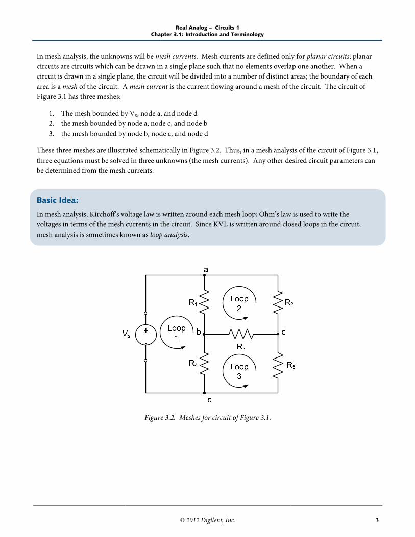
In mesh analysis, the unknowns will be mesh currents. Mesh currents are defined only for planar circuits; planarcircuits are circuits which can be drawn in a single plane such that no elements overlap one another. When acircuit is drawn in a single plane, the circuit will be divided into a number of distinct areas; the boundary of eacharea is a mesh of the circuit. A mesh current is the current flowing around a mesh of the circuit. The circuit ofFigure 3.1 has three meshes:
1. The mesh bounded by VS, node a, and node d2. the mesh bounded by node a, node c, and node b3. the mesh bounded by node b, node c, and node d
These three meshes are illustrated schematically in Figure 3.2. Thus, in a mesh analysis of the circuit of Figure 3.1,three equations must be solved in three unknowns (the mesh currents). Any other desired circuit parameters canbe determined from the mesh currents.
Basic Idea:
In mesh analysis, Kirchoff’s voltage law is written around each mesh loop; Ohm’s law is used to write thevoltages in terms of the mesh currents in the circuit. Since KVL is written around closed loops in the circuit,mesh analysis is sometimes known as loop analysis.
Figure 3.2. Meshes for circuit of Figure 3.1.
Real Analog – Circuits 1Chapter 3.1: Introduction and Terminology
© 2012 Digilent, Inc. 4
Section Summary:
In nodal analysis:a. Unknowns in the analysis are called the node voltagesb. Node voltages are the voltages at the independent nodes in the circuitc. Two nodes connected by a voltage source are not independent. The voltage source constrains the voltages
at the nodes relative to one another. A node which is not independent is also called dependent. In mesh analysis:
a. Unknowns in the analysis are called mesh currents.b. Mesh currents are defined as flowing through the circuit elements which form the perimeter of the circuit
meshes. A mesh is any enclosed, non-overlapping region in the circuit (when the circuit schematic isdrawn on a piece of paper.
Exercises:
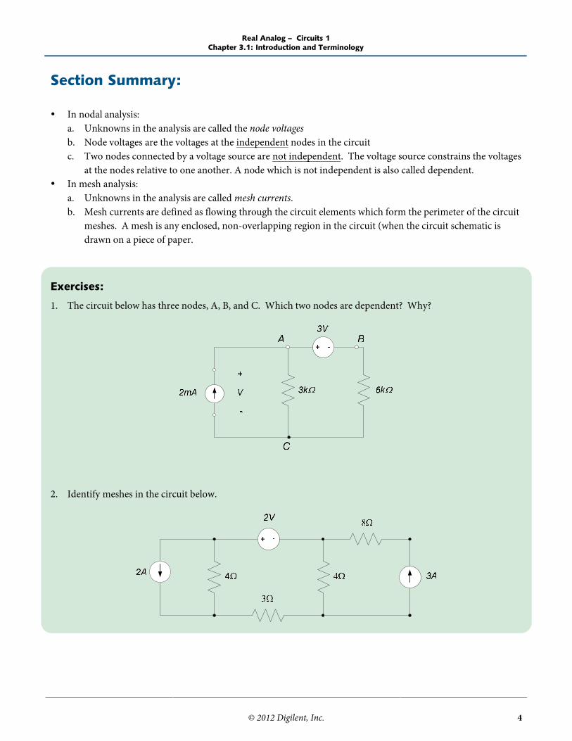
1. The circuit below has three nodes, A, B, and C. Which two nodes are dependent? Why?
2. Identify meshes in the circuit below.

Real Analog – Circuits 1Chapter 3.2: Nodal Analysis
© 2012 Digilent, Inc. 5
3.2: Nodal AnalysisAs noted in section 3.1, in nodal analysis we will define a set of node voltages and use Ohm’s law to writeKirchoff’s current law in terms of these voltages. The resulting set of equations can be solved to determine thenode voltages; any other circuit parameters (e.g. currents) can be determined from these voltages.
The steps used to in nodal analysis are provided below. The steps are illustrated in terms of the circuit of Figure3.3.
Figure 3.3. Example circuit.
Step 1: Define reference voltage
One node will be arbitrarily selected as a reference node or datum node. The voltages of all other nodes in thecircuit will be defined to be relative to the voltage of this node. Thus, for convenience, it will be assumed that thereference node voltage is zero volts. It should be emphasized that this definition is arbitrary – since voltages areactually potential differences, choosing the reference voltage as zero is primarily a convenience.
For our example circuit, we will choose node d as our reference node and define the voltage at this node to be 0V,as shown in Figure 3.4.

Real Analog – Circuits 1Chapter 3.2: Nodal Analysis
© 2012 Digilent, Inc. 6
Figure 3.4. Definition of reference node and reference voltage.
Step 2: Determine independent nodes
We now define the voltages at the independent nodes. These voltages will be the unknowns in our circuitequations. In order to define independent nodes:
“Short-circuit” all voltage sources “Open-circuit” all current sources
After removal of the sources, the remaining nodes (with the exception of the reference node) are defined asindependent nodes. (The nodes which were removed in this process are dependent nodes. The voltages at thesenodes are sometimes said to be constrained.) Label the voltages at these nodes – they are the unknowns for whichwe will solve.
For our example circuit of Figure 1, removal of the voltage source (replacing it with a short circuit) results innodes remaining only at nodes b and c. This is illustrated in Figure 3.5.
Figure 3.5. Independent voltages Vb and Vc.

Real Analog – Circuits 1Chapter 3.2: Nodal Analysis
© 2012 Digilent, Inc. 7
Step 3: Replace sources in the circuit and identify constrained voltages
With the independent voltages defined as in step 2, replace the sources and define the voltages at the dependentnodes in terms of the independent voltages and the known voltage differences.
For our example, the voltage at node a can be written as a known voltage Vs above the reference voltage, as shownin Figure 3.6.
Figure 3.6. Dependent voltages defined.
Step 4: Apply KCL at independent nodes
Define currents and write Kirchoff’s current law at all independent nodes. Currents for our example are shown inFigure 3.7 below. The defined currents include the assumed direction of positive current – this defines the signconvention for our currents. To avoid confusion, these currents are defined consistently with those shown inFigure 3.1(a). The resulting equations are (assuming that currents leaving the node are defined as positive):
Node b:0431 iii (3.1)
Node c:0532 iii (3.2)

Real Analog – Circuits 1Chapter 3.2: Nodal Analysis
© 2012 Digilent, Inc. 8
Figure 3.7. Current definitions and sign conventions.
Step 5: Use Ohm’s law to write the equations from step 4 in terms ofvoltages:
The currents defined in step 4 can be written in terms of the node voltages defined previously. For example, from
Figure 3.7:1
1 RVV
i bS ,3
3 RVV
i cb , and4
40
RV
i b , so equation (3.1) can be written as:
00
431
RV
RVV
RVV bcbbS
So the KCL equation for node b becomes:
Scb VR
VR
VRRR 13431
11111
(3.3)
Likewise, the KCL equation for node c can be written as:
Scb VR
VRRR
VR 25233
11111
(3.4)

Real Analog – Circuits 1Chapter 3.2: Nodal Analysis
© 2012 Digilent, Inc. 9
Double-checking results:
If the circuit being analyzed contains only independent sources, and the sign convention used in the KCLequations is the same as used above (currents leaving nodes are assumed positive), the equations written at eachnode will have the following form:
The term multiplying the voltage at that node will be the sum of the conductances connected to that node.
For the example above, the term multiplying Vb in the equation for node b is431
111RRR while the
term multiplying Vc in the equation for node c is523
111RRR .
The term multiplying the voltages adjacent to the node will be the negative of the conductance connecting
the two nodes. For the example above, the term multiplying Vc in the equation for node b is3
1R , and
the term multiplying Vb in the equation for node c is3
1R .
If the circuit contains dependent sources, or a different sign convention is used when writing the KCL equations,the resulting equations will not necessarily have the above form.
Step 6: Solve the system of equations resulting from step 5
Step 5 will always result in N equations in N unknowns, where N is the number of independent nodes identified instep 2. These equations can be solved for the independent voltages. Any other desired circuit parameters can bedetermined from these voltages.
The example below illustrates the above approach.

Real Analog – Circuits 1Chapter 3.2: Nodal Analysis
© 2012 Digilent, Inc. 10
Example 3.1:
Find the voltage V for the circuit shown below:
Steps 1, 2 and 3: Choosing the reference voltage as shown below, identifying voltages at dependent nodes, anddefining voltages VA and VB at the independent nodes results in the circuit schematic shown below:
+-6V 16A
2 1
2
Referencenode, VR = 0V
Dependentnode, V = 6V VA VB
Steps 4 and 5: Writing KCL at nodes A and B and converting currents to voltages using Ohm’s law results in thefollowing two equations:
Node A:
32311
21
210
120
26
BABA
BAAA VVVVVVVV
Node B:
163165.01
11016
5.00
1
ABAB
BAB VVVVVVV
Step 6: Solving the above equations results in VA = 5V and VB = 7V. The voltage V is
V = VA – VB = -2V.

Real Analog – Circuits 1Chapter 3.2: Nodal Analysis
© 2012 Digilent, Inc. 11
Several comments should be made relative to the above example:
1. Steps 4 and 5 (applying KCL at each independent node and using Ohm’s law to write these equations in termsof voltages) have been combined into a single step. This approach is fairly common, and can provide asignificant savings in time.
2. There may be a perceived inconsistency between the two node equations, in the assumption of positivecurrent direction in the 1 resistor. In the equation for node A, the current is apparently assumed to bepositive from node A to node B, as shown below:
1
VA VBi1
This leads to the corresponding term in the equation for node A becoming: 1BA VV
. In the equation fornode B, however, the positive current direction appears to be from node B to node A, as shown below:
This definition leads to the corresponding term in the equation for node B becoming:1
AB VV .
The above inconsistency in sign is, however, insignificant. Suppose that we had assumed (consistently withthe equation for node A) that the direction of positive current for the node B equation is from node A to B.
Then, the corresponding term in the equation for node B would have been: -1
BA VV (note that a negative
sign has been applied to this term to accommodate our assumption that currents flowing into nodes are
negative). This is equal to1
AB VV , which is exactly what our original result was.
3. The current source appears directly in the nodal equations.
Note:
When we write nodal equations in these chapters, we will generally assume that any unknown currents areflowing away from the node for which we are writing the equation, regardless of any previous assumptions wehave made for the direction of that current. The signs will work out, as long as we are consistent in our signconvention between assumed voltage polarity and current direction and our sign convention relative to positivecurrents flowing out of nodes.
The sign applied to currents induced by current sources must be consistent with the current direction assignedby the source.

Real Analog – Circuits 1Chapter 3.2: Nodal Analysis
© 2012 Digilent, Inc. 12
Supernodes:
In the previous examples, we identified dependent nodes and determined constrained voltages. Kirchoff’s currentlaw was then only written at independent nodes. Many readers find this somewhat confusing, especially if thedependent voltages are not relative to the reference voltage. We will thus discuss these steps in more detail here inthe context of an example, introducing the concept of a supernode in the process.
Example: For the circuit below, determine the voltage difference, V, across the 2mA source.
Step 1: Define reference node
Choose reference node (somewhat arbitrarily) as shown below; label the reference node voltage, VR, as zero volts.

Real Analog – Circuits 1Chapter 3.2: Nodal Analysis
© 2012 Digilent, Inc. 13
Step 2: Define independent nodes
Short circuit voltage sources, open circuit current sources as shown below and identify independentnodes/voltages. For our example, this results in only one independent voltage, labeled as VA below.
Step 3: Replace sources and label any known voltages
The known voltages are written in terms of node voltages identified above. There is some ambiguity in this step.For example, either of the representations below will work equally well – either side of the voltage source can bechosen as the node voltage, and the voltage on the other side of the source written in terms of this node voltage.Make sure, however, that the correct polarity of the voltage source is preserved. In our example, the left side of thesource has a potential that is three volts higher than the potential of the right side of the source. This fact isrepresented correctly by both of the choices below.

Real Analog – Circuits 1Chapter 3.2: Nodal Analysis
© 2012 Digilent, Inc. 14
Step 4: Apply KCL at the independent nodes
It is this step that sometimes causes confusion among readers, particularly when voltage sources are present in thecircuit. Conceptually, it is possible to think of two nodes connected by an ideal voltage source as forming a singlesupernode (some authors use the term generalized node rather than supernode). A node is rigorously defined ashaving a single, unique voltage. However, although the two nodes connected by a voltage source do not share thesame voltage, they are not entirely independent – the two voltages are constrained by one another. This allows usto simplify the analysis somewhat.
For our example, we will arbitrarily choose the circuit to the left above to illustrate this approach. The supernodeis chosen to include the voltage source and both nodes to which it is connected, as shown below. We define twocurrents leaving the supernode, i1 and i2, as shown. KCL, applied at the supernode, results in:
02 21 iimA
As before, currents leaving the node are assumed to be positive. This approach allows us to account for thecurrent flowing through the voltage source without ever explicitly solving for it.
Step 5: Use Ohm’s law to write the KCL equations in terms of voltages
For the single KCL equation written above, this results in:
06
0)3(30
2
k
VkVmA AA
Step 6: Solve the system of equations to determine the nodal voltages
Solution of the equation above results in VA = 5V. Thus, the voltage difference across the current source is V =5V.

Real Analog – Circuits 1Chapter 3.2: Nodal Analysis
© 2012 Digilent, Inc. 15
Alternate Approach: Constraint Equations
The use of supernodes can be convenient, but is not a necessity. An alternate approach, for those who do notwish to identify supernodes, is to retain separate nodes on either side of the voltage source and then write aconstraint equation relating these voltages. Thus, in cases where the reader does not recognize a supernode, theanalysis can proceed correctly. We now revisit the previous example, but use constraint equations rather thanthe previous supernode technique.
In this approach, steps 2 and 3 (identification of independent nodes) are not necessary. One simply writesKirchoff’s current law at all nodes and then writes constraint equations for the voltage sources. A disadvantageof this approach is that currents through voltage sources must be accounted for explicitly; this results in agreater number of unknowns (and equations to be solved) than the supernode technique.
Example (revisited): For the circuit below, determine the voltage difference, V, across the 2mA source.
Choice of a reference voltage proceeds as previously. However, now we will not concern ourselves too muchwith identification of independent nodes. Instead, we will just make sure we account for voltages and currentseverywhere in the circuit. For our circuit, this results in the node voltages and currents shown below. Noticethat we have now identified two unknown voltages (VA and VB) and three unknown currents, one of which (i3)is the current through the voltage source.
Real Analog – Circuits 1Chapter 3.2: Nodal Analysis
© 2012 Digilent, Inc. 16
Now we write KCL at each of the identified nodes, making sure to account for the current through the voltagesource. This results in the following equations (assuming currents leaving the node are positive):
Node A: 02 31 iimA
Node B: 023 ii
Using Ohm’s law to convert the currents i1 and i2 to voltages results in:
Node A: 030
2 3
ikVmA A
Node B: 060
3
kVi B
Notice that we cannot, by inspection, determine anything about the current i3 from the voltages; the voltage-current relationship for an ideal source is not known.
The two equations above have three unknowns – we cannot solve for the node voltages from them without athird equation. This third equation is the constraint equation due to the presence of the voltage source. For ourcircuit, the voltage source causes a direct relationship between VA and VB:
3 AB VV
These three equations (the two KCL equations, written in terms of the node voltages and the constraintequation) constitute three equations in three unknowns. Solving these for the node voltage VA results in VA =5V, so the voltage across the current source is V = 5V.
The example below uses the concept of a supernode to write the governing KCL equations. In the example below,steps 1, 2, and 3 have been condensed into a single process, as have steps 4 and 5. It is suggested that the readerre-do the example below using constraint equations. Note again that the current sources appear directly in theKCL equations.

Real Analog – Circuits 1Chapter 3.2: Nodal Analysis
© 2012 Digilent, Inc. 17
Example 3.2:
For the circuit below, find the power generated or absorbed by the 2V source and the power generated orabsorbed by the 2A source.
Steps 1, 2, and 3: We choose our reference node (arbitrarily) as shown below. Shorting voltage sources and open-circuiting current sources identifies three independent node voltages (labeled below as VA, VB and VC) and onedependent node, with voltage labeled below as VA-2.
+
Steps 4 and 5: Writing KCL at nodes A, B, and C and converting the currents to voltages using Ohm’s law resultsin the equations below. Note that we have (essentially) assumed that all unknown currents at a node are flowingout of the node, consistent with our note 2 for example 1 above.
Node A:
102508)2(
4)2(
40
2
CBACABAA VVVVVVVVVVV
A
Node B:
4237034
)2(30
ABABB VVAVVVVV
Node C:
22038
)2(
ACAC VVAVV
Step 6: Solving the above results in VA = 0V, VB = -6V, and VC = 22V. Thus, the voltage difference across the 2Asource is zero volts, and the 2A source delivers no power. KCL at node A indicates that the current through the2V source is 2A, and the 2V source generates 4W.

Real Analog – Circuits 1Chapter 3.2: Nodal Analysis
© 2012 Digilent, Inc. 18
Dependent Sources:
In the presence of dependent sources, nodal analysis proceeds approximately as outlined above. The maindifference is the presence of additional equations describing the dependent source. As before, we will discuss thetreatment of dependent sources in the context of examples.
Example 3.3:
Write the nodal equations for the circuit below. The dependent source is a voltage controlled voltage source. IS isan independent current source.
As always, the choice of reference node is arbitrary. To determine independent voltages, dependent voltagesources are short-circuited in the same way as independent voltage sources. Thus, the circuit below has twoindependent nodes; the dependent voltage source and the nodes on either side of it form a supernode. Thereference voltage, independent voltages, supernode, and resulting dependent voltage are shown below.
IS
+ -
R3 R4
R2
R1
2Vx Vx+ -
VA VB
Supernode
VA+2Vx
Referencenode, Vr=0
We now, as previously, write KCL for each independent node, taking into account the dependent voltage resultingfrom the presence of the supernode:

Real Analog – Circuits 1Chapter 3.2: Nodal Analysis
© 2012 Digilent, Inc. 19
000)2(
243
RVV
RV
RVV BAAxA
0)2(
12
SxABAB I
RVVV
RVV
The above equations result in a system with two equations and three unknowns: VA, VB, and Vx. (IS is a knowncurrent.) We now write any equations governing the dependent sources. Writing the controlling voltage in termsof the independent voltages results in:
BAx VVV
We now have three equations in three unknowns, which can be solved to determine the independent voltages, VA
and VB.

Real Analog – Circuits 1Chapter 3.2: Nodal Analysis
© 2012 Digilent, Inc. 20
Example 3.4:
Write the nodal equations for the circuit below.
The reference node, independent voltages and dependent voltages are shown on the figure below. A supernode,consisting of the 4V source and the nodes on either side of it, exists but is not shown explicitly on the figure.
+
Applying KCL for each independent node results in:
035
04
0)4(2
3)4(
BAAAA VVVVVVVV
033
xAB IVV
This consists of two equations with three unknowns. The equation governing the dependent current sourceprovides the third equation. Writing the controlling current in terms of independent voltages results in:
50A
xV
I

Real Analog – Circuits 1Chapter 3.2: Nodal Analysis
© 2012 Digilent, Inc. 21
Section Summary:
Basic steps in nodal analysis are:a. Define a reference node. All node voltages will be relative to this reference voltage.b. Identify independent nodes. This can be done by short-circuiting voltage sources, open-circuiting current
sources, and identifying the remaining nodes in the circuit. The voltages at these nodes are the nodevoltages.
c. Determine dependent voltages. This can be done by replacing the sources in the circuit schematic, andwriting voltage constraints introduced by voltage sources.
d. Use Ohm’s law to write KCL at each independent node, in terms of the node voltages. This will result inN equations in N unknowns, where N is the number of node voltages. Independent “nodes” can besupernodes; supernodes typically contain a voltage source; this minimizes the number of equations beingwritten by taking advantage of voltage constraints introduced in step 3.
e. Solve the equations of step 4 to determine the node voltages.f. Use the node voltages to determine any other desired voltages/currents in the circuit.
Modifications to the above approach are allowed. For example, it is not necessary to define supernodes in step4 above. One can define unknown voltages at either terminal of a voltage source and write KCL at each ofthese nodes. However, the unknown current through the voltage source must be accounted for when writingKCL – this introduces an additional unknown into the governing equations. This added unknown requires anadditional equation. This equation is obtained by explicitly writing a constraint equation relating the voltagesat the two terminals of the voltage source.

Real Analog – Circuits 1Chapter 3.2: Nodal Analysis
© 2012 Digilent, Inc. 22
Exercises:
1. Use nodal analysis to write a set of equations from which you can find I1, the current through the 12 resistor.Do not solve the equations.
2. Use nodal analysis to find the current I flowing through the 10 resistor in the circuit below.

Real Analog – Circuits 1Chapter 3.3: Mesh Analysis
© 2012 Digilent, Inc. 23
3.3: Mesh AnalysisIn mesh analysis, we will define a set of mesh currents and use Ohm’s law to write Kirchoff’s voltage law in termsof these voltages. The resulting set of equations can be solved to determine the mesh currents; any other circuitparameters (e.g. voltages) can be determined from these currents.
Mesh analysis is appropriate for planar circuits. Planar circuits can be drawn in a single plane2 such that noelements overlap one another. Such circuits, when drawn in a single plane will be divided into a number ofdistinct areas; the boundary of each area is a mesh of the circuit. A mesh current is the current flowing around amesh of the circuit.
The steps used to in mesh analysis are provided below. The steps are illustrated in terms of the circuit of Figure3.8.
Figure 3.8. Example circuit.
Step 1: Define mesh currents
In order to identify our mesh loops, we will turn off all sources, much like what we did in nodal analysis. To dothis, we Short-circuit all voltage sources Open-circuit all current sources.
Once the sources have been turned off, the circuit can be divided into a number of non-overlapping areas, each ofwhich is completely enclosed by circuit elements. The circuit elements bounding each of these areas form themeshes of our circuit. The mesh currents flow around these meshes. Our example circuit has two meshes afterremoval of the sources, the resulting mesh currents are as shown in Figure 3.9.
Note:
We will always choose our mesh currents as flowing clockwise around the meshes. This assumption is notfundamental to the application of mesh analysis, but it will result in a special form for the resulting equationswhich will later allow us to do some checking of our results.
2 Essentially, you can draw the schematic on a piece of paper without ambiguity.

Real Analog – Circuits 1Chapter 3.3: Mesh Analysis
© 2012 Digilent, Inc. 24
Figure 3.9. Example circuit meshes.
Step 2: Replace sources and identify constrained loops
The presence of current sources in our circuit will result in the removal of some meshes during step 1. We mustnow account for these meshes in our analysis by returning the sources to the circuit and identifying constrainedloops.
We have two rules for constrained loops:
1. Each current source must have one and only one constrained loop passing through it.2. The direction and magnitude of the constrained loop current must agree with the direction and
magnitude of the source current.
For our example circuit, we choose our constrained loop as shown below. It should be noted that constrainedloops can, if desired, cross our mesh loops – we have, however, chosen the constrained loop so that it does notoverlap any of our mesh loops.
Step 3: Write KVL around the mesh loops
We will apply Kirchoff’s voltage law around each mesh loop in order to determine the equations to be solved.Ohm’s law will be used to write KVL in terms of the mesh currents and constrained loop currents as identified insteps 1 and 2 above.
Note that more than one mesh current may pass through a circuit element. When determining voltage dropsacross individual elements, the contributions from all mesh currents passing through that element must beincluded in the voltage drop.

Real Analog – Circuits 1Chapter 3.3: Mesh Analysis
© 2012 Digilent, Inc. 25
When we write KVL for a given mesh loop, we will base our sign convention for the voltage drops on the directionof the mesh current for that loop.
For example, when we write KVL for the mesh current i1 in our example, we choose voltage polarities for resistorsR1 and R4 as shown in the figure below – these polarities agree with the passive sign convention for voltagesrelative to the direction of the mesh current i1.
From the above figure, the voltage drops across the resistor R1 can then be determined as
111 iRV
since only mesh current i1 passes through the resistor R1. Likewise, the voltage drop for the resistor R4 is
)( 2144 iiRV
since mesh currents i1 and i4 both pass through R4 and the current i2 is in the opposite direction to our assumedpolarity for the voltage V4.
Using the above expressions for V1 and V4, we can write KVL for the first mesh loop as:
0)( 21411 iiRiRVS
When we write KVL for the mesh current i2 in our example, we choose voltage polarities for resistors R4, R2, andR5 as shown in the figure below – these polarities agree with the passive sign convention for voltages relative to thedirection of the mesh current i2. Please note that these sign conventions do not need to agree with the signconventions used in the equations for other mesh currents.

Real Analog – Circuits 1Chapter 3.3: Mesh Analysis
© 2012 Digilent, Inc. 26
Using the above sign conventions, KVL for the second mesh loop becomes:
0)()( 2522124 SIiRiRiiR
Please note that the currents i2 and IS are in the same direction in the resistor R5, resulting in a summation of thesecurrents in the term corresponding to the voltage drop across the resistor R5.
Notes:
1. Assumed sign conventions on voltages drops for a particular mesh loop are based on the assumeddirection of that loop’s mesh current.
2. The current passing through an element is the algebraic sum of all mesh and constraint currents passingthrough that element. This algebraic sum of currents is used to determine the voltage drop of theelement.
Step 4: Solve the system of equations to determine the mesh currents ofthe circuit.
Step 3 will always result in N equations in N unknowns, where N is the number of mesh currents identified in step1. These equations can be solved for the mesh currents. Any other desired circuit parameters can be determinedfrom the mesh currents.
The example below illustrates the above approach.

Real Analog – Circuits 1Chapter 3.3: Mesh Analysis
© 2012 Digilent, Inc. 27
Example 3.5:
In the circuit below, determine the voltage drop, V, across the 3 resistor.
Removing the sources results in a single mesh loop with mesh current i1, as shown below.
Replacing the sources and defining one constrained loop per source results in the loop definitions shown below.(Note that each constrained loop goes through only one source and that the amplitude and direction of theconstrained currents agrees with source.)
Applying KVL around the loop i1 and using Ohm’s law to write voltage drops in terms of currents:
AiAiAAiAiV 20)3(4)31(3)1(73 1111
Thus, the current i1 is 2A, in the opposite direction to that shown. The voltage across the 3 resistor is V =3(i1+3A+1A) = 3(-2A+3A+1A) = 3(2A) = 6V.

Real Analog – Circuits 1Chapter 3.3: Mesh Analysis
© 2012 Digilent, Inc. 28
Alternate Approach to Constraint Loops: Constraint Equations
In the above examples, the presence of current sources resulted in a reduced number of meshes. Constraintloops were then used to account for current sources. An alternate approach, in which we retain additional meshcurrents and then apply constraint equations to account for the current sources, is provided here. We use thecircuit of the previous example to illustrate this approach.
Example: Determine the voltage, V, in the circuit below.
Define three mesh currents for each of the three meshes in the above circuit and define unknown voltages V1and V3 across the two current sources as shown below:
Applying KVL around the three mesh loops results in three equations with five unknowns:
0)(7)(3 21311 iiiiV0)(73 312 ViiV04)(3 3133 iiiV
Two additional constraint equations are necessary. These can be determined by the requirement that thealgebraic sum of the mesh currents passing through a current source must equal the current provided by thesource. Thus, we obtain:
Aii 332 Ai 11
Solving the five simultaneous equations above results in the same answer determined previously.

Real Analog – Circuits 1Chapter 3.3: Mesh Analysis
© 2012 Digilent, Inc. 29
Clarification: Constraint loops
Previously, it was claimed that the choice of constraint loops is somewhat arbitrary. The requirements are thateach source has only one constraint loop passing through it, and that the magnitude and direction of theconstrained loop current be consistent with the source. Since constraint loops can overlap other mesh loopswithout invalidating the mesh analysis approach, the choice of constraint loops in not unique. The examplesbelow illustrate the effect of different choices of constraint loops on the analysis of a particular circuit.
Example 3.6 - version 1:
Using mesh analysis, determine the current i through the 4 resistor.
Step 1: Define mesh loops
Replacing the two current sources with open circuits and the two voltage sources with short circuits results in asingle mesh current, i1, as shown below.

Real Analog – Circuits 1Chapter 3.3: Mesh Analysis
© 2012 Digilent, Inc. 30
Step 2: Constrained loops – version 1
Initially, we choose the constrained loops shown below. Note that each loop passes through only one source andhas the magnitude and direction imposed by the source.
Step 3: Write KVL around the mesh loops
Our example has only one mesh current, so only one KVL equation is required. This equation is:
0)(610)2(4)21(28 111 iVAiAAiV
Step 4: Solve the system of equations to determine the mesh currents of the circuit.
Solving the above equation results in i1 = 0.667A. The current through the 4 resistor is then, accounting for the2A constrained loop passing through the resistor, AAii 333.121 .

Real Analog – Circuits 1Chapter 3.3: Mesh Analysis
© 2012 Digilent, Inc. 31
Example 3.6 - version 2:
In this version, we choose an alternate set of constraint loops. The alternate set of loops is shown below; allconstraint loops still pass through only one current source, and retain the magnitude and direction of the sourcecurrent.
Now, writing KVL for the single mesh results in:
0)2(6104)1(28 111 AiViAiV
Solving for the mesh current results in i1 = -1.333A; note that this result is different than previously. However, wedetermine the current through the 4 resistor as i = i1 = -1.333A, which is the same result as previously.
Note:
Choice of alternate constrained loops may change the values obtained for the mesh currents. The currentsthrough the circuit elements, however, do not vary with choice of constrained loops.

Real Analog – Circuits 1Chapter 3.3: Mesh Analysis
© 2012 Digilent, Inc. 32
Example 3.6 - version 3:
In this version, we choose yet another set of constraint loops. These loops are shown below. Again, each looppasses through one current source and retains that source’s current direction and amplitude.
1A+-8V
2
6
i1
2A
+-
10V1A
2A
KVL around the mesh loop results in
0)21(610)1(428 111 AAiVAiiV
Which results in i1 = -0.333A. Again, this is different from the result from out first two approaches. However, thecurrent through the 4 resistor is i = i1 – 1A = -1.333A, which is the same result as previously.
Dependent Sources:
As with nodal analysis, the presence of dependent sources does not significantly alter the overall mesh analysisapproach. The primary difference is simply the addition of the additional equations necessary to describe thedependent sources. We discuss the analysis of circuits with dependent sources in the context of the followingexamples.

Real Analog – Circuits 1Chapter 3.3: Mesh Analysis
© 2012 Digilent, Inc. 33
Example 3.7:
Determine the voltage V in the circuit below.
Shorting both of the voltage sources in the circuit above results in two mesh currents. These are shown in thefigure below.
Writing KVL around the two mesh loops results in
0)(322 211 iiiV04)(32 212 iiiI X
We have two equations and three unknowns. We need an additional equation to solve the system of equations.The third equation is obtained by writing the dependent source’s controlling current in terms of the meshcurrents:
1iI X
The above three equations can be solved to obtain i1 = 0.4375 and i2 = 0.0625. The desired voltageViV 25.04 2 .

Real Analog – Circuits 1Chapter 3.3: Mesh Analysis
© 2012 Digilent, Inc. 34
Example 3.8:
Write the mesh equations for the circuit shown below.
Mesh loops and constraint loops are identified as shown below:
Writing KVL for the two mesh loops results in:
012)3(24 11 VVii X
05)3(312 22 iViV X
Writing the controlling voltage VX in terms of the mesh currents results in:
25 iVX
The above consist of three equations in three unknowns, which can be solved to determine the mesh currents.Any other desired circuit parameters can be determined from the mesh currents.

Real Analog – Circuits 1Chapter 3.3: Mesh Analysis
© 2012 Digilent, Inc. 35
Section Summary:
Basic steps in mesh analysis are:a. Identify mesh currents. This can be done by short-circuiting voltage sources, open-circuiting current
sources, and identifying the enclosed, non-overlapping regions in the circuit. The perimeters of theseareas are the circuit meshes. The mesh currents flow around the circuit meshes
b. Determine constrained loops. The approach in step 1 will ensure that no mesh currents will pass thoughthe current sources. The current source currents can be accounted for by defining constrained loops.Constrained loops are defined as loop currents which pass through the current sources. Constrainedloops are identified by replacing the sources in the circuit schematic, and defining mesh currents whichpass through the current sources; these mesh currents form the constrained loops and must match boththe magnitude and direction of the current in the current sources.
c. Use Ohm’s law to write KVL around each mesh loop, in terms of the mesh currents. This results in Nequations in N unknowns, where N is the number of mesh currents. Keep in mind that the voltagedifference across each element must correspond to the voltage difference induced by all the mesh currentswhich pass through that element.
d. Solve the equations of step 4 to determine the mesh currents.e. Use the mesh currents to determine any other desired voltages/currents in the circuit.
The constrained loops in step 2 above are not unique. Their only requirement is that they must account forthe currents through the current sources.
Modifications to the above approach are allowed. For example, it is not necessary to define constrained loopsin step 3 above. One can define (unknown) mesh currents which pass through through the current sourcesand write KVL for these additional mesh currents. However, the unknown voltage across the current sourcemust be accounted for when writing KVL – this introduces an additional unknown into the governingequations. This added unknown requires an additional equation which is obtained by explicitly writing aconstraint equation equating algebraic sum of the mesh currents passing through a current source to thecurrent provided by the source.

Real Analog – Circuits 1Chapter 3.3: Mesh Analysis
© 2012 Digilent, Inc. 36
Exercises:
1. Use mesh analysis to write a set of equations from which you can find I1, the current through the 12 resistor.Do not solve the equations.
2. Use mesh analysis to find the current I flowing through the 10 resistor in the circuit below. Compare yourresult to your solution to exercise 2 of section 3.2.