1
SR− − 【特徴】はんだコーティングが引きずった様相でソ ルダレジストや基板に傷のある状態の欠陥 【特征】有热风整平时硬拉的摸样,SR 或者板件上有 伤痕的缺陷。 CharacteristicsThere are scratches on solder resist or board surface, which appear to be made by dragging of coated solder. 【原因・判断ポイント・発生工程】基板の反りやク ランプ不適などにより、HALはんだコーティング 時に基板がHAL装置に接触したまま引き上げられ たことにより出来たもの(HAL工程) 【原因、判断要点、发生工序】热风整平时板件翘曲 或者压板不合适等,板件提升时碰撞 HAL 装置所引 起的(HAL工序)。 Causes/processes involved/keys to judgmentA board is dragged while it is in contact with the equipment in HAL solder coating due to the warping of the board or improper clamping. (HAL process) 【特徴】同一端子内や製品内のはんだコーティング の厚さに極端なむらがある状態の欠陥 【特征】在同一个插脚内或者同一种产品内,焊料的 厚度极不均匀的缺陷。 CharacteristicsThere are excessive variations in the thickness of solder coating among lands of a board or among boards of the same type. 【原因・判断ポイント・発生工程】HALの噴射エ ア圧が低すぎたり、エア噴射ノズルが詰まったこと により出来たもの(HAL工程) 【原因、判断要点、发生工序】HAL 喷射风压太低、 或者喷嘴堵塞所引起的(HAL工序)。 Causes/processes involved/keys to judgmentThe defect is caused by too low an air jet pressure or clogging of the air jet nozzles of HAL equipment (HAL process) 4-3-2-3 レベラ傷/热风整平时划伤/ Scratch made in HAL 【コメント】 顕微鏡倍率× 【注释】 显微镜倍率 × ComentsMagnification: × 【コメント】 顕微鏡倍率× 60 【注释】 显微镜倍率 ×60 ComentsMagnification: ×60 4-3-2-4 はんだ厚さむら/焊料的厚度不均匀/ Uneven solder thickness 【コメント】 顕微鏡倍率× 【注释】 显微镜倍率 × ComentsMagnification: × 【コメント】 顕微鏡倍率× 【注释】 显微镜倍率 × ComentsMagnification: × 【コメント】 顕微鏡倍率× 【注释】 显微镜倍率 × ComentsMagnification: ×

4-3-2-3 レベラ傷/热风整平时划伤/ Scratch made in HAL · 2008. 8. 10. · 4-3-2-3 レベラ傷/热风整平时划伤/Scratch made in HAL 【コメント】 顕微鏡倍率×

  • Upload
    others

  • View
    2

  • Download
    0

Embed Size (px)

Citation preview

SR欠陥

シンボルマーク欠陥

めっき欠陥

スルーホール欠陥

機械加工欠陥

その他欠陥

信頼性不足

はんだ上がり欠陥

電子部品実装はんだ周り欠陥

回路欠陥

− ��� −

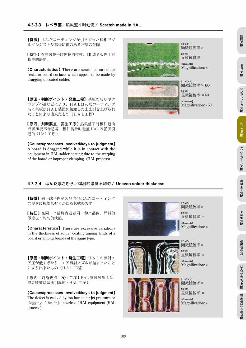
【特徴】はんだコーティングが引きずった様相でソルダレジストや基板に傷のある状態の欠陥

【特征】有热风整平时硬拉的摸样,SR或者板件上有伤痕的缺陷。

【Characteristics】There are scratches on solder resist or board surface, which appear to be made by dragging of coated solder.

【原因・判断ポイント・発生工程】基板の反りやクランプ不適などにより、HALはんだコーティング時に基板がHAL装置に接触したまま引き上げられたことにより出来たもの(HAL工程)

【原因、判断要点、发生工序】 热风整平时板件翘曲或者压板不合适等,板件提升时碰撞 HAL 装置所引起的(HAL 工序)。

【Causes/processes involved/keys to judgment】A board is dragged while it is in contact with the equipment in HAL solder coating due to the warping of the board or improper clamping. (HAL process)

【特徴】同一端子内や製品内のはんだコーティングの厚さに極端なむらがある状態の欠陥

【特征】在同一个插脚内或者同一种产品内,焊料的厚度极不均匀的缺陷。

【Characteristics】There are excessive variations in the thickness of solder coating among lands of a board or among boards of the same type.

【原因・判断ポイント・発生工程】HALの噴射エア圧が低すぎたり、エア噴射ノズルが詰まったことにより出来たもの(HAL工程)

【原因、判断要点、发生工序】 HAL 喷射风压太低、或者喷嘴堵塞所引起的(HAL 工序)。

【Causes/processes involved/keys to judgment】The defect is caused by too low an air jet pressure or clogging of the air jet nozzles of HAL equipment (HAL process)

4-3-2-3 レベラ傷/热风整平时划伤/ Scratch made in HAL

【コメント】

顕微鏡倍率×【注释】

显微镜倍率×

【Coments】

Magnification: ×

【コメント】

顕微鏡倍率× 60【注释】

显微镜倍率×60

【Coments】

Magnification: ×60

4-3-2-4 はんだ厚さむら/焊料的厚度不均匀/ Uneven solder thickness

【コメント】

顕微鏡倍率×【注释】

显微镜倍率×

【Coments】

Magnification: ×

【コメント】

顕微鏡倍率×【注释】

显微镜倍率×

【Coments】

Magnification: ×

【コメント】

顕微鏡倍率×【注释】

显微镜倍率×

【Coments】

Magnification: ×