Embed Size (px)
Citation preview

Springer Series in Advanced Microelectronics 48
Amir Zjajo
StochasticProcess Variationin Deep-Submicron CMOSCircuits and Algorithms

Springer Series in Advanced Microelectronics
Volume 48
Series Editors
Dr. Kiyoo Itoh, Kokubunji-shi, Tokyo, JapanProf. Thomas H. Lee, Stanford, CA, USAProf. Takayasu Sakurai, Minato-ku, Tokyo, JapanProf. Willy M. C. Sansen, Leuven, BelgiumProf. Doris Schmitt-Landsiedel, Munich, Germany
For further volumes:http://www.springer.com/series/4076

The Springer Series in Advanced Microelectronics provides systematic informa-tion on all the topics relevant for the design, processing, and manufacturing ofmicroelectronic devices. The books, each prepared by leading researchers orengineers in their fields, cover the basic and advanced aspects of topics such aswafer processing, materials, device design, device technologies, circuit design,VLSI implementation, and sub-system technology. The series forms a bridgebetween physics and engineering, therefore the volumes will appeal to practicingengineers as well as research scientists.

Amir Zjajo
Stochastic Process Variationin Deep-Submicron CMOS
Circuits and Algorithms
123

Amir ZjajoElectrical Engineering, Mathematics and
Computer ScienceDelft University of TechnologyDelftThe Netherlands
ISSN 1437-0387 ISSN 2197-6643 (electronic)ISBN 978-94-007-7780-4 ISBN 978-94-007-7781-1 (eBook)DOI 10.1007/978-94-007-7781-1Springer Dordrecht Heidelberg New York London
Library of Congress Control Number: 2013950725
� Springer Science+Business Media Dordrecht 2014This work is subject to copyright. All rights are reserved by the Publisher, whether the whole or part ofthe material is concerned, specifically the rights of translation, reprinting, reuse of illustrations,recitation, broadcasting, reproduction on microfilms or in any other physical way, and transmission orinformation storage and retrieval, electronic adaptation, computer software, or by similar or dissimilarmethodology now known or hereafter developed. Exempted from this legal reservation are briefexcerpts in connection with reviews or scholarly analysis or material supplied specifically for thepurpose of being entered and executed on a computer system, for exclusive use by the purchaser of thework. Duplication of this publication or parts thereof is permitted only under the provisions ofthe Copyright Law of the Publisher’s location, in its current version, and permission for use mustalways be obtained from Springer. Permissions for use may be obtained through RightsLink at theCopyright Clearance Center. Violations are liable to prosecution under the respective Copyright Law.The use of general descriptive names, registered names, trademarks, service marks, etc. in thispublication does not imply, even in the absence of a specific statement, that such names are exemptfrom the relevant protective laws and regulations and therefore free for general use.While the advice and information in this book are believed to be true and accurate at the date ofpublication, neither the authors nor the editors nor the publisher can accept any legal responsibility forany errors or omissions that may be made. The publisher makes no warranty, express or implied, withrespect to the material contained herein.
Printed on acid-free paper
Springer is part of Springer Science+Business Media (www.springer.com)

To my family

Acknowledgments
The Author acknowledges the contributions of Drs. Nick van der Meijs, MichelBerkelaar, Rene van Leuken and Sumeet Kumar of Delft University of Technology,Prof. Dr. Jose Pineda de Gyvez and Dr. Alessandro Di Bucchianico of EindhovenUniversity of Technology, Dr. Manuel Barragan of University of Seville, Dr. QinTang of Institute of Technology Research for Solid State Lighting, Chagzhou,China, Arnica Aggarwal of ASLM Holding, Veldhoven, The Netherlands, RadhikaJagtap of ARM Holdings, Cambridge, UK, and Javier Rodriguez of StruktonRolling Stock, Alblasserdam, The Netherlands.
vii
Contents
1 Introduction . . . . . . . . . . . . . . . . . . . . . . . . . . . . . . . . . . . . . . . . 11.1 Stochastic Process Variations in Deep-Submicron CMOS. . . . . . 11.2 Remarks on Current Design Practice . . . . . . . . . . . . . . . . . . . . 51.3 Motivation . . . . . . . . . . . . . . . . . . . . . . . . . . . . . . . . . . . . . . 131.4 Organization of the Book . . . . . . . . . . . . . . . . . . . . . . . . . . . . 14References . . . . . . . . . . . . . . . . . . . . . . . . . . . . . . . . . . . . . . . . . . 15
2 Random Process Variation in Deep-Submicron CMOS . . . . . . . . . 172.1 Modeling Process Variability . . . . . . . . . . . . . . . . . . . . . . . . . 192.2 Stochastic MNA for Process Variability Analysis . . . . . . . . . . . 232.3 Statistical Timing Analysis . . . . . . . . . . . . . . . . . . . . . . . . . . . 27
2.3.1 Statistical Simplified Transistor Model . . . . . . . . . . . . . 292.3.2 Bounds on Statistical Delay . . . . . . . . . . . . . . . . . . . . . 312.3.3 Reducing Computational Complexity . . . . . . . . . . . . . . 33
2.4 Yield Constrained Energy Optimization . . . . . . . . . . . . . . . . . . 372.4.1 Optimum Energy Point . . . . . . . . . . . . . . . . . . . . . . . . 382.4.2 Optimization Problem . . . . . . . . . . . . . . . . . . . . . . . . . 40
2.5 Experimental Results . . . . . . . . . . . . . . . . . . . . . . . . . . . . . . . 412.6 Conclusions . . . . . . . . . . . . . . . . . . . . . . . . . . . . . . . . . . . . . 49References . . . . . . . . . . . . . . . . . . . . . . . . . . . . . . . . . . . . . . . . . . 50
3 Electrical Noise in Deep-Submicron CMOS . . . . . . . . . . . . . . . . . 553.1 Stochastic MNA for Noise Analysis. . . . . . . . . . . . . . . . . . . . . 563.2 Accuracy Considerations . . . . . . . . . . . . . . . . . . . . . . . . . . . . 593.3 Adaptive Numerical Integration Methods . . . . . . . . . . . . . . . . . 62
3.3.1 Deterministic Euler–Maruyama Scheme. . . . . . . . . . . . . 633.3.2 Deterministic Milstein Scheme . . . . . . . . . . . . . . . . . . . 64
3.4 Estimation of the Noise Content Contribution . . . . . . . . . . . . . . 653.5 Experimental Results . . . . . . . . . . . . . . . . . . . . . . . . . . . . . . . 673.6 Conclusions . . . . . . . . . . . . . . . . . . . . . . . . . . . . . . . . . . . . . 80References . . . . . . . . . . . . . . . . . . . . . . . . . . . . . . . . . . . . . . . . . . 81
ix
4 Temperature Effects in Deep-Submicron CMOS . . . . . . . . . . . . . . 834.1 Thermal Model . . . . . . . . . . . . . . . . . . . . . . . . . . . . . . . . . . . 854.2 Temperature Estimation . . . . . . . . . . . . . . . . . . . . . . . . . . . . . 914.3 Reducing Computation Complexity . . . . . . . . . . . . . . . . . . . . . 95
4.3.1 Modified Runge–Kutta Solver . . . . . . . . . . . . . . . . . . . 954.3.2 Adaptive Error Control . . . . . . . . . . . . . . . . . . . . . . . . 974.3.3 Balanced Stochastic Truncation Model
Order Reduction . . . . . . . . . . . . . . . . . . . . . . . . . . . . . 984.4 System Level Methodology for Temperature Constrained
Power Management . . . . . . . . . . . . . . . . . . . . . . . . . . . . . . . . 994.4.1 Overview of the Methodology . . . . . . . . . . . . . . . . . . . 1004.4.2 Temperature-Power Simulation . . . . . . . . . . . . . . . . . . . 102
4.5 Experimental Results . . . . . . . . . . . . . . . . . . . . . . . . . . . . . . . 1054.6 Conclusions . . . . . . . . . . . . . . . . . . . . . . . . . . . . . . . . . . . . . 112References . . . . . . . . . . . . . . . . . . . . . . . . . . . . . . . . . . . . . . . . . . 112
5 Circuit Solutions . . . . . . . . . . . . . . . . . . . . . . . . . . . . . . . . . . . . . 1175.1 Architecture of the System . . . . . . . . . . . . . . . . . . . . . . . . . . . 1185.2 Circuits for Active Monitoring of Temperature
and Process Variation . . . . . . . . . . . . . . . . . . . . . . . . . . . . . . 1215.2.1 Die-Level Variation Monitoring Circuits . . . . . . . . . . . . 1215.2.2 Detector and Interface Circuit. . . . . . . . . . . . . . . . . . . . 1235.2.3 Temperature Monitor. . . . . . . . . . . . . . . . . . . . . . . . . . 125
5.3 Characterization of Process Variability Conditions . . . . . . . . . . 1275.3.1 Optimized Design Environment . . . . . . . . . . . . . . . . . . 1275.3.2 Test-Limit Updates and Guidance . . . . . . . . . . . . . . . . . 129
5.4 Experimental Results . . . . . . . . . . . . . . . . . . . . . . . . . . . . . . . 1315.5 Conclusions . . . . . . . . . . . . . . . . . . . . . . . . . . . . . . . . . . . . . 146References . . . . . . . . . . . . . . . . . . . . . . . . . . . . . . . . . . . . . . . . . . 146
6 Conclusions and Recommendations. . . . . . . . . . . . . . . . . . . . . . . . 1496.1 Summary of the Results . . . . . . . . . . . . . . . . . . . . . . . . . . . . . 1496.2 Recommendations and Future Research . . . . . . . . . . . . . . . . . . 152References . . . . . . . . . . . . . . . . . . . . . . . . . . . . . . . . . . . . . . . . . . 156
Appendix . . . . . . . . . . . . . . . . . . . . . . . . . . . . . . . . . . . . . . . . . . . . . 157
About the Author . . . . . . . . . . . . . . . . . . . . . . . . . . . . . . . . . . . . . . . 187
Index . . . . . . . . . . . . . . . . . . . . . . . . . . . . . . . . . . . . . . . . . . . . . . . . 189
x Contents

Abbreviations
A/D Analog to DigitalADC Analog to Digital ConverterALU Arithmetic Logic UnitAWE Asymptotic Waveform EvaluationBDF Backward Differentiation FormulaBSIM Berkeley Short-Channel IGFET ModelCAD Computer Aided DesignCDF Cumulative Distribution FunctionCMOS Complementary MOSCMP Chip MultiprocessorCPU Central Processing UnitD/A Digital to AnalogDAC Digital to Analog ConverterDAE Differential Algebraic EquationsDEM Dynamic Element MatchingDFT Discrete Fourier TransformDIBL Drain-Induced Barrier LoweringDLL Delay-Locked LoopDLPVM Die-Level Process Variation MonitorDNL Differential NonlinearityDR Dynamic RangeDSP Digital Signal ProcessorDSPMR Dominant Subspaces Projection Model ReductionDSTA Deterministic Static Timing AnalysisDTFT Discrete Time Fourier TransformDVFS Dynamic Voltage–Frequency ScalingEDA Electronic Design AutomationEKF Extended Kalman FilterEM Expectation-MaximizationENOB Effective Number of BitsERBW Effective Resolution BandwidthFFT Fast Fourier TransformFPGA Field Programmable Gate ArrayGBW Gain-Bandwidth Product
xi

IC Integrated CircuitIEEE Institute of Electrical and Electronics EngineersINL Integral NonlinearityITDFT Inverse Time Discrete Fourier TransformKCL Kirchhoff’ Current LawKF Kalman FilterLMS Least Mean SquareLSB Least Significant BitLUT Lookup TableML Maximum LikelihoodMNA Modified Nodal AnalysisMOS Metal Oxide SemiconductorMOSFET Metal Oxide Semiconductor Field Emitter TransistorMPSoC Multi Processor System on ChipMISS Multiple Input Simultaneous SwitchingMLE Maximum Likelihood EstimationMOR Model Order ReductionMSE Mean Square ErrorMSB Most Significant BitNA Nodal AnalysisNMOS Negative doped MOSODE Ordinary Differential EquationOTA Operational Transconductance AmplifierPCB Printed Circuit BoardPCM Process Control MonitoringPDE Partial Differential EquationPDF Probability Density FunctionPE Processing ElementPGA Programmable Gain AmplifierPLL Phase Locked LoopPMB Power Management BlockPMOS Positive doped MOSPSRR Power Supply Rejection RatioPTAT Proportional to Absolute TemperatureRDF Random Doping FluctuationsRMSE Root Mean Square ErrorRTN Random Telegraph NoiseSC Switched CapacitorSDE Stochastic Differential EquationSDM Steepest Descent MethodSFDR Spurious Free Dynamic RangeSINAD Signal-to-Noise and DistortionSNR Signal-to-Noise RatioSNDR Signal-to-Noise plus Distortion RatioSOI Silicon on Insulator
xii Abbreviations

SPICE Simulation Program with Integrated Circuit EmphasisSoC System on ChipSSTA Statistical Static Timing AnalysisSTA Static Timing AnalysisSTI Shallow Trench IsolationSVD Singular Value DecompositionSVM Support Vector MachineTAP Test Access PortTBR Truncated Balanced RealizationTCB Test Control BlockTDC Time to Digital ConverterTSV Through Silicon ViaTHD Total Harmonic DistortionUKF Unscented Kalman FilterUT Unscented TransformVGA Variable Gain AmplifierVLSI Very Large-Scale Integrated CircuitWSS Wide Sense Stationary
Abbreviations xiii

Symbols
a Elements of the incidence matrix A, circuit activity factorA Amplitude, area, constant singular incidence matrixAf Voltage gain of feedback amplifierb Number of circuit branchesBi Number of output codesB Bit, effective stage resolutionBn Noise bandwidthci Class to which the data xi from the input vector belongscxy Process correction factors depending upon the process maturitych(i) Highest achieved normalized fault coveragecV Capacitance of the volume VC* Neyman–Pearson Critical regionC Capacitance, covariance matrixCC Compensation capacitance, cumulative coverageCeff Effective capacitanceCG Gate capacitance, input capacitance of the operational amplifierCGS Gate-Source capacitanceCin Input capacitanceCL Load capacitanceCout Parasitic output capacitanceCox Gate-oxide capacitanceCpar Parasitic capacitanceCtot Total load capacitanceCQ Function of the deterministic initial solutionCNN Autocorrelation matrixC11 Symmetrical covariance matrixCH[] Cumulative histogramdi Location of transistor i on the die with respect to a point of origindj Delay of path jDi Multiplier of reference voltageDout Digital outputDT Total number of devices
xv

e Noise, error, scaling parameter of transistor currenteq Quantization errore2 Noise powerEconv Energy per conversion stepEtotal Total energyfclk Clock frequencyfin Input frequencyfp, n(di) Eigenfunctions of the covariance matrixfS Sampling frequencyfsig Signal frequencyfspur Frequency of spurious tonefT Transit frequencyf(x, t) Vector of noise intensitiesFQ Function of the deterministic initial solutiong ConductanceGi Interstage gainGm Transconductanceh Numerical integration step size, surface heat transfer coefficienti Index, circuit node, transistor on the dieimax number of iteration stepsI CurrentIamp Total amplifier current consumptionIdiff Diffusion currentID Drain currentIDD Power supply currentIref Reference currentj Index, circuit branchJ0 Jacobian of the initial data z0 evaluated at pi
k Boltzmann’s coefficient, error correction coefficient, indexK Amplifier current gain, gain error correction coefficientK(t) Variance-covariance matrix of k(t)l() Likelihood functionL Channel lengthLi Low rank Cholesky factorsLR Length of the measurement recordL(h|TX) Log-likelihood of parameter h with respect to input set TX
m Number of different stage resolutions, indexM Number of termsn Index, number of circuit nodes, number of faults in a listN Number of bits, piecewise linear Galerkin basis functionNaperture Aperture jitter limited resolutionP Powerp Process parameter
xvi Symbols

p(di, h) Stochastic process corresponding to process parameter ppX|H(x|h) Gaussian mixture modelp* Process parameter deviations from their corresponding nominal valuesp1 Dominant pole of amplifierp2 Non-dominant pole of amplifierq Channel charge, circuit nodes, index, vector of state variablesQ Quality factor, heat sourceQi Number of quantization steps, cumulative probabilityQ(x) Normal accumulation probability functionQ(h|h(t)) Auxiliary function in EM algorithmr Circuit nodes, number of iterationsR Resistancerds Output resistance of a transistorReff Effective thermal resistanceRon Switch on-resistanceRn-1 Process noise covariancerout Amplifier output resistanceSi SiliconSn Output vector of temperatures at sensor locationss Scaling parameter of transistor size, observed converter staget TimeT Absolute temperature, transpose, test stimulitox Oxide thicknesstS Sampling timevf Fractional part of the analog input signalun Gaussian sensor noiseUBi Upper bound of the ith levelV VoltageVBB Body-bias voltageVDD Positive supply voltageVDS Drain-source voltageVDS, SAT Drain-source saturation voltageVFS Full-scale voltageVGS Gate-source voltageVbe Base-emitter voltageVin Input voltageVLSB Voltage corresponding to the least significant bitVmargin Safety margin of drain-source saturation voltageVoff Offset voltageVres Residue voltageVT Threshold voltagew Normal vector perpendicular to the hyperplane, weightwi Cost of applying test stimuli performing test number i
Symbols xvii

W Channel width, Wiener process parameter vector, loss functionW*, L* Geometrical deformation due to manufacturing variationsx Vector of unknownsxi Vectors of observationsx(t) Analog input signalX Input, observability Gramiany0 Arbitrary initial state of the circuity[k] Output digital signaly YieldY Output, controllability Gramianz0 Nominal voltages and currentsz(1-a) (1-a)-quantile of the standard normal distribution Zz[k] Reconstructed output signalZ Low rank Cholesky factora Neyman–Pearson significance level, weight vector of the training setb Feedback factor, transistor current gain, boundc Noise excess factor, measurement correction factor, reference errorsci Iteration shift parametersd Relative mismatche Errorf Distributed random variable, forgetting factorg Random vector, Galerkin test function, stage gain errorsh Die, unknown parameter vector, coefficients of mobility reductionhp, n Eigenvalues of the covariance matrixj Converter transition codek Threshold of significance level a, white noise processkj Central value of the transition bandl Carrier mobility, mean value, iteration step sizem Fitting parameter estimated from the extracted datan(t) Vector of independent Gaussian white noise sourcesni Degree of misclassification of the data xi
nn(h) Vector of zero-mean uncorrelated Gaussian random variablesq Correlation parameter reflecting the spatial scale of clustering1p Random vector accounting for device tolerancesr Standard deviationra Gain mismatch standard deviationrb Bandwidth mismatch standard deviationrd Offset mismatch standard deviationrr Time mismatch standard deviationUn Measurement noise covariances Time constantU Set of all valid design variable vectors in design spaceu Clock phase
xviii Symbols

/T Thermal voltage at the actual temperaturev Circuit performance functionUr, f [.] Probability functionD Relative deviationK Linearity of the rampNr Boundaries of voltage of interestR Covariance matrixX Sample space of the test statistics
Symbols xix
Chapter 1Introduction
1.1 Stochastic Process Variationsin Deep-Submicron CMOS
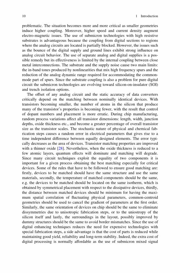
The CMOS technology has dominated the mainstream silicon IC industry in thelast few decades. As CMOS integrated circuits are moving into unprecedentedoperating frequencies and accomplishing unprecedented integration levels(Fig. 1.1), potential problems associated with device scaling—the short-channeleffects—are also looming large as technology strides into the deep-submicronregime. Besides that it is costly to add sophisticated process options to controlthese side effects, the compact device modeling of short-channel transistors hasbecome a major challenge for device physicists. In addition, the loss of certaindevice characteristics, such as the square-law I–V relationship, adversely affectsthe portability of the circuits designed in an older generation of technology.Smaller transistors also exhibit relatively larger statistical variations of manydevice parameters (i.e., doping density, oxide thickness, threshold voltage etc.).The resultant large spread of the device characteristics also causes severe yieldproblems for both analog and digital circuits.
The most profound reason for the increase in parameter variability is that thetechnology is approaching the regime of fundamental randomness in the behaviorof silicon structures where device operation must be described as a stochasticprocess. Statistical fluctuations of the channel dopant number pose a fundamentalphysical limitation of MOSFETs down-scaling. Entering into the nanometerregime results in a decreasing number of channel impurities whose random dis-tribution leads to significant fluctuations of the threshold voltage and off-stateleakage current. These variations are true random variations with no correlationacross devices and induce serious problems on the operation and performances oflogical and analog circuits. Such random variations can also result from a group ofother sources, such as lithography, etching, chemical mechanical polishing etc.With each generation of device scaling, the total number of active dopants in thechannel region decreases to the extent that, when the device gate length is scaledbelow sub-100 nm, the dopant distribution can be considered random where the
A. Zjajo, Stochastic Process Variation in Deep-Submicron CMOS, Springer Seriesin Advanced Microelectronics 48, DOI: 10.1007/978-94-007-7781-1_1,� Springer Science+Business Media Dordrecht 2014
1

channel is formed. Consequently, a few defects at the Si/SiO2 interface or insidethe SiO2 dielectric are sufficient to cause device failure when the dopant distri-bution becomes fully random across the channel region. The compound betweenrandom dopant fluctuations (RDF) in active channel region and underlyingdepletion region and other sources of variation, such as random telegraph noisecaused by the random capture and release of charge carriers by traps located in aMOS transistor’s oxide layer, further complicates the situation especially inextremely scaled CMOS design. Despite advances in resolution enhancementtechniques [1], lithographic variation continues to be a challenge for sub-90 nmtechnologies.
At the same time, aggressive scaling has also resulted in many non-lithographicsources of variation such as dopant variation [2], well-proximity effects [3], layoutdependent stress variation in strained silicon technologies [4], and rapid thermalanneal temperature induced variation [5, 6]. These variation sources must becharacterized and modeled for improved model-to-hardware correlation. Thecontribution of fabrication process steps dominates the electrical parameter vari-ations of a device with aggressive device scaling such as oxidation, ion implan-tation, lithography and chemical mechanical planarization. Moreover, the effectsof random variations in circuit operating conditions such as the temperature andthe power supply voltage VDD increases dramatically as the circuit clock frequencyincreases [7]. This has led to significant variations in the circuit performance andincreased yield degradation as the performance of a circuit is governed by thelinear and non-linear electrical behavior of its individual devices. Variations inelectrical characteristics of these devices (Appendix A) make the performance ofthe circuit deviate from its intended values and cause performance degradation.
Fig. 1.1 a Left, first working integrated circuit, 1958, (Copyright � Texas Instruments: Source–www.ti.com–public domain), b middle, Intel Pentium processor fabricated in 0.8 lm technologycontaining 3.1 million transistors, 1993, c right, Intel Ivy Bridge processor fabricated in 22 nmtechnology containing over 1.4 billion transistors, 2012 (Copyright � Intel Corporation: Source–www.intel.com–public domain)
2 1 Introduction
The physical deviation of manufacturing processes such as implantation dose andenergy cause a variation in device structure and doping profile. These variationstogether with the environmental variation sources affect the electrical behavior ofdevice and result in performance metric variations of the circuit and the overallperformance of a system on a chip (SoC). Variations in materials and gas flow (linearvariation) or due the wafer spin process and exposure time (radial) variations [8] aresources of the inter-die variation, which is regarded as a shift in the mean or expectedvalue of a parameter equally across all devices on any one die. Conversely, waferlevel variations and layout-dependent variations [9] are sources of intra-die varia-tions (deviations from designed values across different locations in the die). Thewafer level variations originate due to effects such as lens aberrations and result inbowl-shaped or other known distributions over the entire reticle [10]. As a conse-quence, it can result in small trends which represent the spatial range across the die.While the layout-dependent or die-pattern variations are due to lithographic andetching techniques used during process fabrication including process steps such aschemical mechanical polishing and optical proximity correction, these dependenciescreate additional variations, e.g. due to photo-lithographic interactions and plasmaetch micro-loading [9, 10] two interconnected lines designed identically in differentparts of the same die may result in lines with different widths.
Both analog and digital variation-aware design approaches require on-chipprocess variation and temperature monitors or measurement circuits. For digitalsystems, variation monitors based on ring oscillators or delay lines for speedassessments [11, 12] and temperature sensors for power density management[13–15] have been employed. Temperature fluctuations alter threshold voltage,carrier mobility, and saturation velocity of a MOSFET. Temperature fluctuationinduced variations in individual device parameters have unique effects on MOStransistor drain current. The dominant parameter that determines circuit speedvaries with the device/circuit bias conditions. At higher supply voltages, the drainsaturation current of a MOS transistor degrades when the temperature is increased.Alternatively, provided that the supply voltage is low, transistor drain currentincreases with temperature, indicating a change in the dominant device parameter.As the levels of integration and number of processor cores increase (e.g. 80 coresin [16]), the adaptive methods will become more effective when the number ofpartitions with local process variation and temperature monitors is also increased.Nevertheless, the die area of the monitors and routing must be minimized to avoidexcessive fabrication cost. In microprocessors and other digitally-intensive sys-tems manage on-chip power dissipation and temperature is managed usingnumerous variable supply voltages or clock frequencies for different sections(cores) on the die [17, 18]. These techniques directly benefit from the informationprovided by the distributed placement of the sensors with sensitivity to static anddynamic power. A major advantage of variation-sensing approaches for on-chipcalibration of circuits is the enhanced resilience to the process and environmentalvariations that are presently creating yield and reliability challenges for chipsfabricated with widely used CMOS technology. Since the threshold voltage is asignificant process variation indicator for analog [19] and digital circuits [20],
1.1 Stochastic Process Variations in Deep-Submicron CMOS 3
there are existing methods to monitor its statistical variation [21]. In digitalsections, the local operating frequency/speed measurements supplied by the var-iation monitors provides information in adaptive body bias methods and otherapproaches to cope with worsening within-die variations in CMOS technologies[22, 23]. In digitally-intensive systems, the extracted information that representslocal on-die variations is sufficient to enable on-chip power and thermal man-agement techniques by applying variable supply voltages or clock frequencies inthe different sections (cores) [17, 18, 24]. In general, the continued enhancement ofon-chip local variation-sensing capabilities to assess the digital performanceindicators will allow more reductions of variation and aging effects [13].
The analog-to-digital interface circuit exhibits keen sensitivity to technologyscaling. To achieve high linearity, high dynamic range, and high sampling speedsimultaneously under low supply voltages in deep-submicron CMOS technologywith low power consumption has thus far been conceived of as extremely chal-lenging. The impact of random dopant fluctuation is exhibited through a large VT
and accounts for most of the variations observed in analog circuits where sys-tematic variation is small and random uncorrelated variation can cause mismatch(e.g. stochastic fluctuation of parameter mismatch is often referred to with the termmatching) that results in reduced noise margins. In general, to cope with thedegradation in device properties, several design techniques have been applied,starting with manual trimming in the early days, followed by analog techniquessuch as chopper stabilization, auto-zeroing techniques (correlated double sam-pling), dynamic element matching, dynamic current mirrors and current copiers.However, these techniques are not able to reduce the intrinsic random telegraphnoise in MOSFETs; the reduction factor is typically limited by device mismatch,timing errors and charge injection.
In an effort to reduce random telegraph noise, the self correlation of thephysical noisy process should be obstructed; the noise could be reduced by a rapidswitching between two states such as periodic large signal excitation (switchedbias technique) [25]: one state that is characterized by a significant generation oflow-frequency noise and another state that is characterized by a negligible amountof low-frequency noise. Although such a method could probably be used to reducethe low frequency noise dominated by random telegraph noise, overall low-fre-quency noise would increase as the normally ‘dormant’ traps under steady-stateconditions get active as a result of the dynamic biasing.
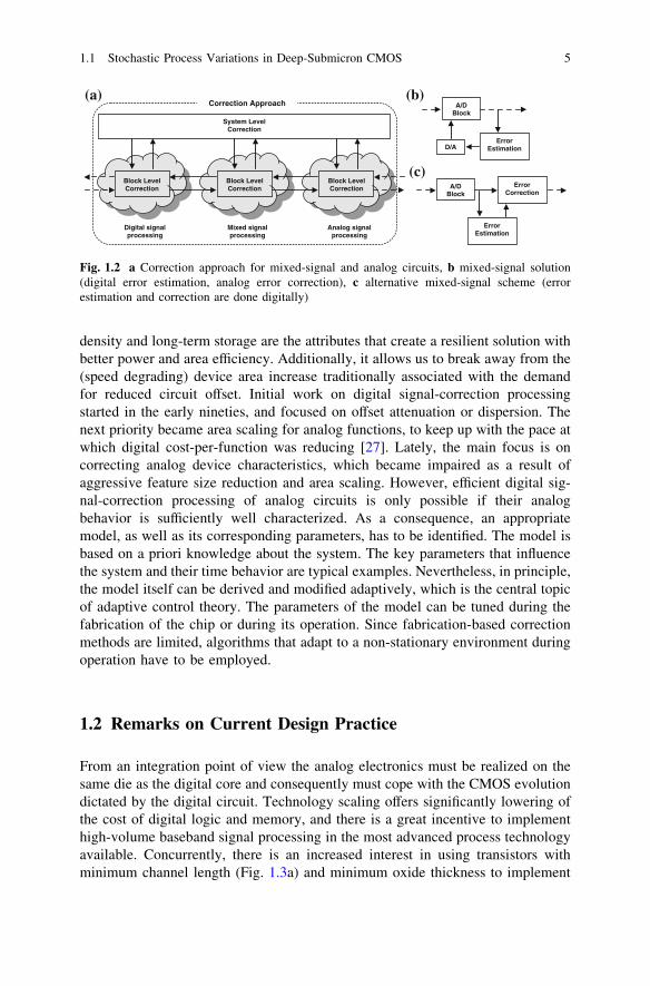
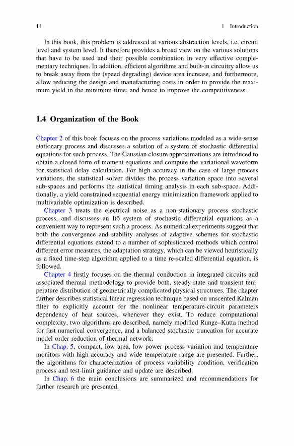
Nowadays digital signal-correction processing is exploited to compensate forsignal impairments created by analog device imperfections on both block andsystem level [26] (Fig. 1.2). System level correction uses system knowledge toimprove or simplify block level correction tasks. In contrast, block level correctionrefers to the improvement of the overall performance of a particular block in thesystem. In the mixed-signal blocks, due to additional digital post- or pre-pro-cessing, the boundaries between analog signal processing and digital signal pro-cessing become blurred. Because of the increasing analog/digital performance gapand the flexibility of digital circuits, performance-supporting digital circuits are anintrinsic part of mixed-signal and analog circuits. In this approach, integration
4 1 Introduction
density and long-term storage are the attributes that create a resilient solution withbetter power and area efficiency. Additionally, it allows us to break away from the(speed degrading) device area increase traditionally associated with the demandfor reduced circuit offset. Initial work on digital signal-correction processingstarted in the early nineties, and focused on offset attenuation or dispersion. Thenext priority became area scaling for analog functions, to keep up with the pace atwhich digital cost-per-function was reducing [27]. Lately, the main focus is oncorrecting analog device characteristics, which became impaired as a result ofaggressive feature size reduction and area scaling. However, efficient digital sig-nal-correction processing of analog circuits is only possible if their analogbehavior is sufficiently well characterized. As a consequence, an appropriatemodel, as well as its corresponding parameters, has to be identified. The model isbased on a priori knowledge about the system. The key parameters that influencethe system and their time behavior are typical examples. Nevertheless, in principle,the model itself can be derived and modified adaptively, which is the central topicof adaptive control theory. The parameters of the model can be tuned during thefabrication of the chip or during its operation. Since fabrication-based correctionmethods are limited, algorithms that adapt to a non-stationary environment duringoperation have to be employed.
1.2 Remarks on Current Design Practice
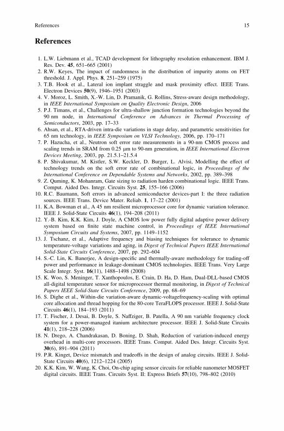
From an integration point of view the analog electronics must be realized on thesame die as the digital core and consequently must cope with the CMOS evolutiondictated by the digital circuit. Technology scaling offers significantly lowering ofthe cost of digital logic and memory, and there is a great incentive to implementhigh-volume baseband signal processing in the most advanced process technologyavailable. Concurrently, there is an increased interest in using transistors withminimum channel length (Fig. 1.3a) and minimum oxide thickness to implement
Block Level Correction
Analog signal processing
Block Level Correction
Mixed signal processing
Block Level Correction
Digital signal processing
System Level Correction
Correction Approach
ErrorCorrection
ErrorEstimation
A/DBlock
ErrorEstimation
A/DBlock
D/A
(a) (b)
(c)
Fig. 1.2 a Correction approach for mixed-signal and analog circuits, b mixed-signal solution(digital error estimation, analog error correction), c alternative mixed-signal scheme (errorestimation and correction are done digitally)
1.1 Stochastic Process Variations in Deep-Submicron CMOS 5

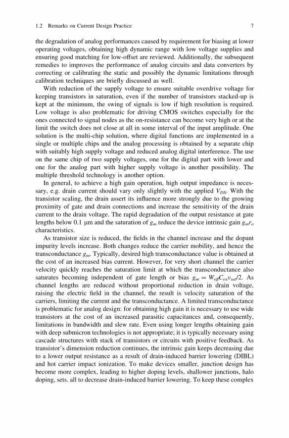
analog functions, because the improved device transition frequency, fT, allows forfaster operation. To ensure sufficient lifetime for digital circuitry and to keeppower consumption at an acceptable level, the dimension-reduction is accompa-nied by lowering of nominal supply voltages. Due to the reduction of supplyvoltage the available signal swing is lowered, fundamentally limiting theachievable dynamic range at reasonable power consumption levels. Additionally,lower supply voltages require biasing at lower operating voltages which results inworse transistor properties, and hence yield circuits with lower performance. Toachieve a high linearity, high sampling speed, high dynamic range, with lowsupply voltages and low power dissipation in ultra-deep-submicron CMOS tech-nology is a major challenge.
The key limitation of analog circuits is that they operate with electrical vari-ables and not simply with discrete numbers that, in circuit implementations, givesrise of a beneficial noise margin. On the contrary, the accuracy of analog circuitsfundamentally relies on matching between components, low noise, offset and lowdistortions. In this section, the most challenging design issues for low voltage,high-resolution A/D converters in deep submicron technologies such as contrasting
Year
Line
Wid
th [n
m]
Line width
Syp
ply
Vol
tage
[V],
GB
W [G
Hz]
GBW
Supply
20152008200319980
50
100
150
200
0.1
1
10
100
1000
12
IDS [A]
GB
W [G
Hz] 90 nm
CL=200 fF
0.25 µm
CL=100 fF
CL=200 fF
CL=100 fF
0
2
4
6
8
10
0 0.25 0.75 1.25 1.75
(a)
(b)
Fig. 1.3 a Trend of analogfeatures in CMOStechnologies, b gain-bandwidth product versusdrain current in twotechnological nodes
6 1 Introduction
the degradation of analog performances caused by requirement for biasing at loweroperating voltages, obtaining high dynamic range with low voltage supplies andensuring good matching for low-offset are reviewed. Additionally, the subsequentremedies to improves the performance of analog circuits and data converters bycorrecting or calibrating the static and possibly the dynamic limitations throughcalibration techniques are briefly discussed as well.
With reduction of the supply voltage to ensure suitable overdrive voltage forkeeping transistors in saturation, even if the number of transistors stacked-up iskept at the minimum, the swing of signals is low if high resolution is required.Low voltage is also problematic for driving CMOS switches especially for theones connected to signal nodes as the on-resistance can become very high or at thelimit the switch does not close at all in some interval of the input amplitude. Onesolution is the multi-chip solution, where digital functions are implemented in asingle or multiple chips and the analog processing is obtained by a separate chipwith suitably high supply voltage and reduced analog digital interference. The useon the same chip of two supply voltages, one for the digital part with lower andone for the analog part with higher supply voltage is another possibility. Themultiple threshold technology is another option.
In general, to achieve a high gain operation, high output impedance is neces-sary, e.g. drain current should vary only slightly with the applied VDS. With thetransistor scaling, the drain assert its influence more strongly due to the growingproximity of gate and drain connections and increase the sensitivity of the draincurrent to the drain voltage. The rapid degradation of the output resistance at gatelengths below 0.1 lm and the saturation of gm reduce the device intrinsic gain gmro
characteristics.As transistor size is reduced, the fields in the channel increase and the dopant
impurity levels increase. Both changes reduce the carrier mobility, and hence thetransconductance gm. Typically, desired high transconductance value is obtained atthe cost of an increased bias current. However, for very short channel the carriervelocity quickly reaches the saturation limit at which the transconductance alsosaturates becoming independent of gate length or bias gm = WeffCoxvsat/2. Aschannel lengths are reduced without proportional reduction in drain voltage,raising the electric field in the channel, the result is velocity saturation of thecarriers, limiting the current and the transconductance. A limited transconductanceis problematic for analog design: for obtaining high gain it is necessary to use widetransistors at the cost of an increased parasitic capacitances and, consequently,limitations in bandwidth and slew rate. Even using longer lengths obtaining gainwith deep submicron technologies is not appropriate; it is typically necessary usingcascade structures with stack of transistors or circuits with positive feedback. Astransistor’s dimension reduction continues, the intrinsic gain keeps decreasing dueto a lower output resistance as a result of drain-induced barrier lowering (DIBL)and hot carrier impact ionization. To make devices smaller, junction design hasbecome more complex, leading to higher doping levels, shallower junctions, halodoping, sets. all to decrease drain-induced barrier lowering. To keep these complex
1.2 Remarks on Current Design Practice 7
junctions in place, the annealing steps formerly used to remove damage andelectrically active defects must be curtailed, increasing junction leakage.
Heavier doping also is associated with thinner depletion layers and morerecombination centers that result in increased leakage current, even without latticedamage. In addition, gate leakage currents in very thin-oxide devices will set anupper bound on the attainable effective output resistance via circuit techniques(such as active cascade). Similarly, as scaling continues, the elevated drain-to-source leakage in an off-switch can adversely affect the switch performance. Ifthe switch is driven by an amplifier, the leakage may lower the output resistance ofthe amplifier, hence limits its low-frequency gain.
Low-distortion at quasi-dc frequencies is relevant for many analog circuits.Typically, quasi-dc distortion may be due to the variation of the depletion layerwidth along the channel, mobility reduction, velocity saturation and nonlinearitiesin the transistors’ transconductances and in their output conductances, which isheavily dependent on biasing, size, technology and typically sees large voltageswings. With scaling higher harmonic components may increase in amplitudedespite the smaller signal; the distortion increases significantly. At circuit level thedegraded quasi-dc performance can be compensated by techniques that boost gain,such as (regulated) cascodes. These are, however, harder to fit within decreasingsupply voltages. Other solutions include a more aggressive reduction of signalmagnitude which requires a higher power consumption to maintain SNR levels.
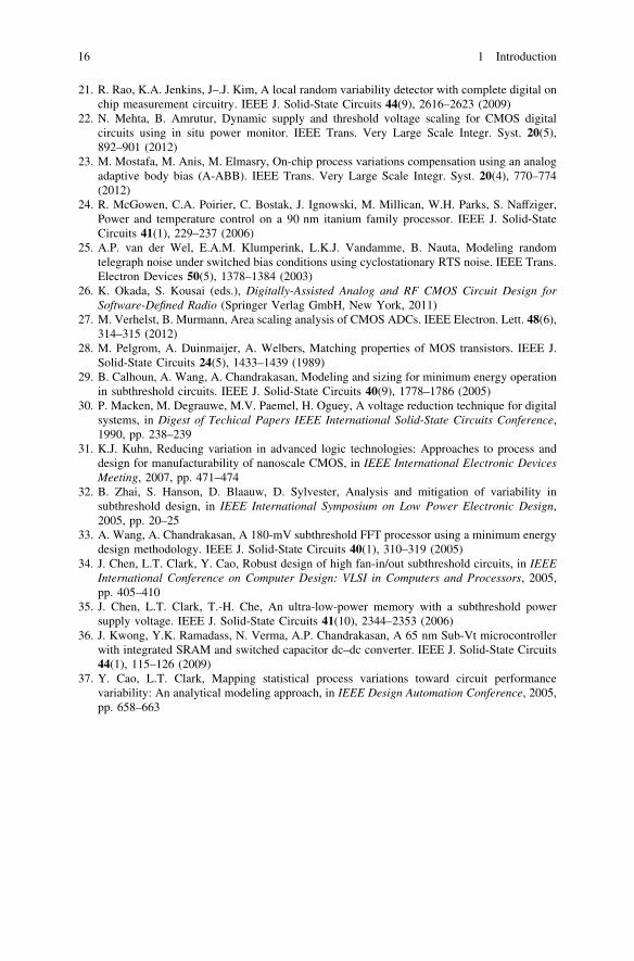
The theoretically highest gain-bandwidth of an OTA is almost determined bythe cutoff frequency of transistor (see Fig. 1.3b for assessment of GBW for twotechnological nodes). Assuming that the kT/C noise limit establishes the value ofthe load capacitance, to achieve required SNR large transconductance is required.Accordingly, the aspect ratio necessary for the input differential pair must be fairlylarge, in the 100 range. Similarly, since with scaling the gate oxide becomesthinner, the specific capacitance Cox increases as the scaling factor. However, sincethe gate area decreases as the square of the scaling factor, the gate-to-source andgain-to-drain parasitic capacitance lowers as the process is scaled. The coefficientsfor the parasitic input and output capacitance, Cgs and Cgd shown in Fig. 1.4a havebeen obtained by simulation for conventional foundry processes under theassumption that the overdrive voltage is 0.175 V. Similarly, with technology-scaling the actual junctions become shallower, roughly proportional to the tech-nology feature size. Also, the junction area roughly scales in proportion to theminimum gate-length, while the dope level increase does not significantly increasethe capacitance per area. Altogether this leads to a significantly reduced junctioncapacitance per gm with newer technologies. Reducing transistor parasitic capac-itance is desired, however, the benefit is contrasted by the increased parasiticcapacitance of the interconnection (the capacitance of the wires connecting dif-ferent parts of the chip). With transistors becoming smaller and more transistorsbeing placed on the chip, interconnect capacitance is becoming a large percentageof total capacitance.
The global effect is that scaling does not benefit fully from the scaling inincreasing the speed of analog circuit as the position of the non-dominant poles is
8 1 Introduction

largely unchanged. Additionally, with the reduced signal swing, to achieverequired SNR signal capacitance has to increase proportionally. By examiningFig. 1.4b, it can be seen that the characteristic exhibits convex curve and takes thehighest value at the certain sink current (region b). In the region of the currentbeing less than this value (region a), the conversion frequency increases with anincrease of the sink current. Similarly, in the region of the current being higherthan this value (region c), the conversion frequency decreases with an increase ofthe sink current.
There are two reasons why this characteristic is exhibited; in the low currentregion, the gm is proportional to the sink current, and the parasitic capacitances aresmaller than the signal capacitance. At around the peak, at least one of the parasiticcapacitances becomes equal to the signal capacitance. In the region of the currentbeing larger than that value, both parasitic capacitances become larger than thesignal capacitance and the conversion frequency will decrease with an increase ofthe sink current.
In mixed signal application the substrate noise and the interference betweenanalog and digital supply voltages caused by the switching of digital sections are
L[µm]
C[fF
/mA
], f T
[GH
z], W
[µm
/mA
]
Cgs W
fT
1/s 2
Cgd
0.1 0.2 0.3 0.4 0.5 1
10
100
500
IDS [A]
f C [M
z]
90 nm
0.25 µm
a 0.18 µm
0.13µm
b c
0.01 0.1 10 1 10
100
1k
10k
(a)
(b)
Fig. 1.4 a Scaling of gatewidth and transistorcapacitances, b conversionfrequency fc versus draincurrent for four technologicalnodes
1.2 Remarks on Current Design Practice 9
problematic. The situation becomes more and more critical as smaller geometriesinduce higher coupling. Moreover, higher speed and current density augmentelectro-magnetic issues. The use of submicron technologies with high resistivesubstrates is advantageous because the coupling from digital sections to regionswhere the analog circuits are located is partially blocked. However, the issues suchas the bounce of the digital supply and ground lines exhibit strong influence onanalog circuit behavior. The use of separate analog and digital supplies is a pos-sible remedy but its effectiveness is limited by the internal coupling between closemetal interconnections. The substrate and the supply noise cause two main limits:the in-band tones produced by nonlinearities that mix high frequency spurs and thereduction of the analog dynamic range required for accommodating the common-mode part of spurs. Since the substrate coupling is also a problem for pure digitalcircuit the submicron technologies are evolving toward silicon-on-insulator (SOI)and trench isolation options.
The offset of any analog circuit and the static accuracy of data converterscritically depend on the matching between nominally identical devices. Withtransistors becoming smaller, the number of atoms in the silicon that producemany of the transistor’s properties is becoming fewer, with the result that controlof dopant numbers and placement is more erratic. During chip manufacturing,random process variations affect all transistor dimensions: length, width, junctiondepths, oxide thickness etc., and become a greater percentage of overall transistorsize as the transistor scales. The stochastic nature of physical and chemical fab-rication steps causes a random error in electrical parameters that gives rise to atime independent difference between equally designed elements. The error typi-cally decreases as the area of devices. Transistor matching properties are improvedwith a thinner oxide [28]. Nevertheless, when the oxide thickness is reduced to afew atomic layers, quantum effects will dominate and matching will degrade.Since many circuit techniques exploit the equality of two components it isimportant for a given process obtaining the best matching especially for criticaldevices. Some of the rules that have to be followed to ensure good matching are:firstly, devices to be matched should have the same structure and use the samematerials, secondly, the temperature of matched components should be the same,e.g. the devices to be matched should be located on the same isotherm, which isobtained by symmetrical placement with respect to the dissipative devices, thirdly,the distance between matched devices should be minimum for having the maxi-mum spatial correlation of fluctuating physical parameters, common-centroidgeometries should be used to cancel the gradient of parameters at the first order.Similarly, the same orientation of devices on chip should be the same to eliminatedissymmetries due to unisotropic fabrication steps, or to the uniostropy of thesilicon itself and lastly, the surroundings in the layout, possibly improved bydummy structures should be the same to avoid border mismatches. Since the use ofdigital enhancing techniques reduces the need for expensive technologies withspecial fabrication steps, a side advantage is that the cost of parts is reduced whilemaintaining good yield, reliability and long-term stability. Indeed, the extra cost ofdigital processing is normally affordable as the use of submicron mixed signal
10 1 Introduction

technologies allows for efficient usage of silicon area even for relatively complexalgorithms. The methods can be classified into foreground and backgroundcalibration.
The foreground calibration, typical of A/D converters, interrupts the normaloperation of the converter for performing the trimming of elements or the mis-match measurement by a dedicated calibration cycle normally performed atpower-on or during periods of inactivity of the circuit. Any miscalibration orsudden environmental changes such as power supply or temperature may make themeasured errors invalid. Therefore, for devices that operate for long periods it isnecessary to have periodic extra calibration cycles. The input switch restores thedata converter to normal operational after the mismatch measurement and everyconversion period the logic uses the output of the A/D converter to properlyaddress the memory that contains the correction quantity. In order to optimize thememory size the stored data should be the minimum word-length, which dependson technology accuracy and expected A/D linearity. The digital measure of errors,that allows for calibration by digital signal processing, can be at the element, blockor entire converter level. The calibration parameters are stored in memories but, incontrast with the trimming case, the content of the memories is frequently used, asthey are input of the digital processor.
Methods using background calibration work during the normal operation of theconverter by using extra circuitry that functions all the time synchronously withthe converter function.
Often these circuits use hardware redundancy to perform a background cali-bration on the fraction of the architecture that is not temporarily used. However,since the use of redundant hardware is effective but costs silicon area and powerconsumption, other methods aim at obtaining the functionality by borrowing asmall fraction of the sampled-data circuit operation for performing the self-calibration.
Power-management has evolved from static custom-hardware optimization tohighly dynamic run-time monitoring, assessing, and adapting of hardware per-formance and energy with precise awareness of the instantaneous applicationdemands. In order to support an ultra dynamic voltage scaling system, logic cir-cuits must be capable of operating across a wide voltage range, from nominal VDD
down to the minimum energy point which optimizes the energy per operation. Thisoptimum point typically lies in the subthreshold region [29], below the transistorthreshold voltage VT. Although voltage scaling within the above-threshold regionis a well-known technique [4, 30], extending this down to subthreshold posesparticular challenges due to reduced ION/IOFF and process variation. In sub-threshold, drive current of the on devices ION is several orders of magnitude lowerthan in strong inversion. Correspondingly, the ratio of active to idle leakagecurrents ION/IOFF is much reduced. In digital logic, this implies that the idleleakage in the off devices counteract the on devices, such that the on devices maynot pull the output of a logic gate fully to VDD or ground. Moreover, local processvariation can further skew the relative strengths of transistors on the same chip,increasing delay variability and adversely impacting functionality of logic gates.
1.2 Remarks on Current Design Practice 11

A number of effects contribute to local variation, including random dopantfluctuation (RDF), line-edge roughness, and local oxide thickness variations [31].Effects of RDF, in which placement and number of dopant atoms in the devicechannel cause random VT shifts, are especially pronounced in subthreshold [32]since these VT shifts lead directly to exponential changes in device currents.
To address these challenges, logic circuits in sub-VT should be designed toensure sufficient ION/IOFF in the presence of global and local variation. In [33] alogic gate design methodology is provided, which accounts for global processcorners, and identify logic gates with severely asymmetric pullup/pulldown net-works (should be avoided in sub-VT). In [34], analytical models were derived forthe output voltage and minimum functional VDD of circuits, such as in register files[35], where many parallel leaking devices oppose the active device. One approachto mitigate local variation is to increase the sizes of transistors [28] at a cost ofhigher leakage and switched capacitance. Accordingly, a transistor sizing meth-odology is described in [36] to manage the trade-off between reducing variabilityand minimizing energy overhead. In addition to affecting logic functionality,process variation increases circuit delay uncertainty by up to an order of magni-tude in sub-VT. As a result, statistical methodologies are thus needed to fullycapture the wide delay variations seen at very low voltages. Whereas the rela-tionship between delay and VT is approximately linear in above-threshold, itbecomes exponential in sub-VT, and timing analysis techniques for low-voltagedesigns must adapt accordingly. Nominal delay and delay variability models validin both above- and subthreshold regions are presented in [37], while analyticalexpressions for sub-VT logic gate and logic path delays were derived in [32].
While dynamic voltage scaling is a popular method to minimize power con-sumption in digital circuits given a performance constraint, the same circuits arenot always constrained to their performance-intensive mode during regular oper-ation. There are long spans of time when the performance requirement is highlyrelaxed.
There are also certain emerging energy-constrained applications where mini-mizing the energy required to complete operations is the main concern. For boththese scenarios, operating at the minimum energy operating voltage of digitalcircuits has been proposed as a solution to minimize energy [33].
The minimum energy point arises from opposing trends in the dynamic andleakage energy per clock cycle as VDD scales down. The dynamic CVDD
2 energydecreases quadratically, but in the subthreshold region, the leakage energy percycle increases as a result of the leakage power being integrated over exponen-tially longer clock periods. With process scaling, the shrinking of feature sizesimplies smaller switching capacitances and thus lower dynamic energy. At thesame time, leakage current in recent technology generations have increased sub-stantially, in part due to VT being decreased to maintain performance while thenominal supply voltage is scaled down. The minimum energy point is not a fixedvoltage for a given circuit, and can vary widely depending on its workload andenvironmental conditions (e.g., temperature). Any relative increase in the activeenergy component of the circuit due to an increase in the workload or activity of
12 1 Introduction

the circuit decreases the minimum energy operating voltage. On the other hand, arelative increase of the leakage energy component due to an increase in temper-ature or the duration of leakage over an operation pushes the minimum energyoperating voltage to go up. This makes the circuit go faster thereby not allowingthe circuit to leak for a longer time.
1.3 Motivation
With the fast advancement of CMOS fabrication technology, more and moresignal-processing functions are implemented in the digital domain for a lower cost,lower power consumption, higher yield, and higher re-configurability. This hasrecently generated a great demand for low-power, low-voltage circuits that can berealized in a mainstream deep-submicron CMOS technology. However, the dis-crepancies between lithography wavelengths and circuit feature sizes areincreasing. Lower power supply voltages significantly reduce noise margins andincrease variations in process, device and design parameters. Consequently, it issteadily more difficult to control the fabrication process precisely enough tomaintain uniformity. The inherent randomness of materials used in fabrication atnanoscopic scales means that performance will be increasingly variable, not onlyfrom die-to-die but also within each individual die. Parametric variability will becompounded by degradation in nanoscale integrated circuits resulting in instabilityof parameters over time, eventually leading to the development of faults. Processvariation cannot be solved by improving manufacturing tolerances; variabilitymust be reduced by new device technology or managed by design in order forscaling to continue.
In addition to device variability, which sets the limitations of circuit designs interms of accuracy, linearity and timing, existence of electrical noise associatedwith fundamental processes in integrated-circuit devices represents an elementarylimit on the performance of electronic circuits. Similarly, higher temperatureincreases the risk of damaging the devices and interconnects (since major back-endand front-end reliability issues including electromigration, time-dependentdielectric breakdown, and negative-bias temperature instability have strongdependence on temperature), even with advanced thermal managementtechnologies.
The relevance of process variations, electrical noise and temperature to theeconomics of the semiconductor and EDA markets is in its strong correlation withprocess yield. If designed in a traditional way, design margins will have to be sorelaxed that they will pose serious treat for any integrated circuit developmentproject. Consequently, accurate variability estimation presents a particular chal-lenge and is expected to be one of the foremost steps in the evaluation of suc-cessful high-performance circuit designs.
1.2 Remarks on Current Design Practice 13
In this book, this problem is addressed at various abstraction levels, i.e. circuitlevel and system level. It therefore provides a broad view on the various solutionsthat have to be used and their possible combination in very effective comple-mentary techniques. In addition, efficient algorithms and built-in circuitry allow usto break away from the (speed degrading) device area increase, and furthermore,allow reducing the design and manufacturing costs in order to provide the maxi-mum yield in the minimum time, and hence to improve the competitiveness.
1.4 Organization of the Book
Chapter 2 of this book focuses on the process variations modeled as a wide-sensestationary process and discusses a solution of a system of stochastic differentialequations for such process. The Gaussian closure approximations are introduced toobtain a closed form of moment equations and compute the variational waveformfor statistical delay calculation. For high accuracy in the case of large processvariations, the statistical solver divides the process variation space into severalsub-spaces and performs the statistical timing analysis in each sub-space. Addi-tionally, a yield constrained sequential energy minimization framework applied tomultivariable optimization is described.
Chapter 3 treats the electrical noise as a non-stationary process stochasticprocess, and discusses an Itô system of stochastic differential equations as aconvenient way to represent such a process. As numerical experiments suggest thatboth the convergence and stability analyses of adaptive schemes for stochasticdifferential equations extend to a number of sophisticated methods which controldifferent error measures, the adaptation strategy, which can be viewed heuristicallyas a fixed time-step algorithm applied to a time re-scaled differential equation, isfollowed.
Chapter 4 firstly focuses on the thermal conduction in integrated circuits andassociated thermal methodology to provide both, steady-state and transient tem-perature distribution of geometrically complicated physical structures. The chapterfurther describes statistical linear regression technique based on unscented Kalmanfilter to explicitly account for the nonlinear temperature-circuit parametersdependency of heat sources, whenever they exist. To reduce computationalcomplexity, two algorithms are described, namely modified Runge–Kutta methodfor fast numerical convergence, and a balanced stochastic truncation for accuratemodel order reduction of thermal network.
In Chap. 5, compact, low area, low power process variation and temperaturemonitors with high accuracy and wide temperature range are presented. Further,the algorithms for characterization of process variability condition, verificationprocess and test-limit guidance and update are described.
In Chap. 6 the main conclusions are summarized and recommendations forfurther research are presented.
14 1 Introduction
References
1. L.W. Liebmann et al., TCAD development for lithography resolution enhancement. IBM J.Res. Dev. 45, 651–665 (2001)
2. R.W. Keyes, The impact of randomness in the distribution of impurity atoms on FETthreshold. J. Appl. Phys. 8, 251–259 (1975)
3. T.B. Hook et al., Lateral ion implant straggle and mask proximity effect. IEEE Trans.Electron Devices 50(9), 1946–1951 (2003)
4. V. Moroz, L. Smith, X.-W. Lin, D. Pramanik, G. Rollins, Stress-aware design methodology,in IEEE International Symposium on Quality Electronic Design, 2006
5. P.J. Timans, et al., Challenges for ultra-shallow junction formation technologies beyond the90 nm node, in International Conference on Advances in Thermal Processing ofSemiconductors, 2003, pp. 17–33
6. Ahsan, et al., RTA-driven intra-die variations in stage delay, and parametric sensitivities for65 nm technology, in IEEE Symposium on VLSI Technology, 2006, pp. 170–171
7. P. Hazucha, et al., Neutron soft error rate measurements in a 90-nm CMOS process andscaling trends in SRAM from 0.25 lm to 90-nm generation, in IEEE International ElectronDevices Meeting, 2003, pp. 21.5.1–21.5.4
8. P. Shivakumar, M. Kistler, S.W. Keckler, D. Burger, L. Alvisi, Modelling the effect oftechnology trends on the soft error rate of combinational logic, in Proceedings of theInternational Conference on Dependable Systems and Networks, 2002, pp. 389–398
9. Z. Quming, K. Mohanram, Gate sizing to radiation harden combinational logic. IEEE Trans.Comput. Aided Des. Integr. Circuits Syst. 25, 155–166 (2006)
10. R.C. Baumann, Soft errors in advanced semiconductor devices-part I: the three radiationsources. IEEE Trans. Device Mater. Reliab. 1, 17–22 (2001)
11. K.A. Bowman et al., A 45 nm resilient microprocessor core for dynamic variation tolerance.IEEE J. Solid-State Circuits 46(1), 194–208 (2011)
12. Y.-B. Kim, K.K. Kim, J. Doyle, A CMOS low power fully digital adaptive power deliverysystem based on finite state machine control, in Proceedings of IEEE InternationalSymposium Circuits and Systems, 2007, pp. 1149–1152
13. J. Tschanz, et al., Adaptive frequency and biasing techniques for tolerance to dynamictemperature-voltage variations and aging, in Digest of Technical Papers IEEE InternationalSolid-State Circuits Conference, 2007, pp. 292–604
14. S.-C. Lin, K. Banerjee, A design-specific and thermally-aware methodology for trading-offpower and performance in leakage-dominant CMOS technologies. IEEE Trans. Very LargeScale Integr. Syst. 16(11), 1488–1498 (2008)
15. K. Woo, S. Meninger, T. Xanthopoulos, E. Crain, D. Ha, D. Ham, Dual-DLL-based CMOSall-digital temperature sensor for microprocessor thermal monitoring, in Digest of TechnicalPapers IEEE Solid-State Circuits Conference, 2009, pp. 68–69
16. S. Dighe et al., Within-die variation-aware dynamic-voltagefrequency-scaling with optimalcore allocation and thread hopping for the 80-core TeraFLOPS processor. IEEE J. Solid-StateCircuits 46(1), 184–193 (2011)
17. T. Fischer, J. Desai, B. Doyle, S. Naffziger, B. Patella, A 90 nm variable frequency clocksystem for a power-managed itanium architecture processor. IEEE J. Solid-State Circuits41(1), 218–228 (2006)
18. N. Drego, A. Chandrakasan, D. Boning, D. Shah, Reduction of variation-induced energyoverhead in multi-core processors. IEEE Trans. Comput. Aided Des. Integr. Circuits Syst.30(6), 891–904 (2011)
19. P.R. Kinget, Device mismatch and tradeoffs in the design of analog circuits. IEEE J. Solid-State Circuits 40(6), 1212–1224 (2005)
20. K.K. Kim, W. Wang, K. Choi, On-chip aging sensor circuits for reliable nanometer MOSFETdigital circuits. IEEE Trans. Circuits Syst. II: Express Briefs 57(10), 798–802 (2010)
References 15
21. R. Rao, K.A. Jenkins, J–.J. Kim, A local random variability detector with complete digital onchip measurement circuitry. IEEE J. Solid-State Circuits 44(9), 2616–2623 (2009)
22. N. Mehta, B. Amrutur, Dynamic supply and threshold voltage scaling for CMOS digitalcircuits using in situ power monitor. IEEE Trans. Very Large Scale Integr. Syst. 20(5),892–901 (2012)
23. M. Mostafa, M. Anis, M. Elmasry, On-chip process variations compensation using an analogadaptive body bias (A-ABB). IEEE Trans. Very Large Scale Integr. Syst. 20(4), 770–774(2012)
24. R. McGowen, C.A. Poirier, C. Bostak, J. Ignowski, M. Millican, W.H. Parks, S. Naffziger,Power and temperature control on a 90 nm itanium family processor. IEEE J. Solid-StateCircuits 41(1), 229–237 (2006)
25. A.P. van der Wel, E.A.M. Klumperink, L.K.J. Vandamme, B. Nauta, Modeling randomtelegraph noise under switched bias conditions using cyclostationary RTS noise. IEEE Trans.Electron Devices 50(5), 1378–1384 (2003)
26. K. Okada, S. Kousai (eds.), Digitally-Assisted Analog and RF CMOS Circuit Design forSoftware-Defined Radio (Springer Verlag GmbH, New York, 2011)
27. M. Verhelst, B. Murmann, Area scaling analysis of CMOS ADCs. IEEE Electron. Lett. 48(6),314–315 (2012)
28. M. Pelgrom, A. Duinmaijer, A. Welbers, Matching properties of MOS transistors. IEEE J.Solid-State Circuits 24(5), 1433–1439 (1989)
29. B. Calhoun, A. Wang, A. Chandrakasan, Modeling and sizing for minimum energy operationin subthreshold circuits. IEEE J. Solid-State Circuits 40(9), 1778–1786 (2005)
30. P. Macken, M. Degrauwe, M.V. Paemel, H. Oguey, A voltage reduction technique for digitalsystems, in Digest of Techical Papers IEEE International Solid-State Circuits Conference,1990, pp. 238–239
31. K.J. Kuhn, Reducing variation in advanced logic technologies: Approaches to process anddesign for manufacturability of nanoscale CMOS, in IEEE International Electronic DevicesMeeting, 2007, pp. 471–474
32. B. Zhai, S. Hanson, D. Blaauw, D. Sylvester, Analysis and mitigation of variability insubthreshold design, in IEEE International Symposium on Low Power Electronic Design,2005, pp. 20–25
33. A. Wang, A. Chandrakasan, A 180-mV subthreshold FFT processor using a minimum energydesign methodology. IEEE J. Solid-State Circuits 40(1), 310–319 (2005)
34. J. Chen, L.T. Clark, Y. Cao, Robust design of high fan-in/out subthreshold circuits, in IEEEInternational Conference on Computer Design: VLSI in Computers and Processors, 2005,pp. 405–410
35. J. Chen, L.T. Clark, T.-H. Che, An ultra-low-power memory with a subthreshold powersupply voltage. IEEE J. Solid-State Circuits 41(10), 2344–2353 (2006)
36. J. Kwong, Y.K. Ramadass, N. Verma, A.P. Chandrakasan, A 65 nm Sub-Vt microcontrollerwith integrated SRAM and switched capacitor dc–dc converter. IEEE J. Solid-State Circuits44(1), 115–126 (2009)
37. Y. Cao, L.T. Clark, Mapping statistical process variations toward circuit performancevariability: An analytical modeling approach, in IEEE Design Automation Conference, 2005,pp. 658–663
16 1 Introduction
Chapter 2Random Process Variationin Deep-Submicron CMOS
One of the most notable features of nanometer scale CMOS technology is theincreasing magnitude of variability of the key parameters affecting performance ofintegrated circuits [1]. Although scaling made controlling extrinsic variabilitymore complex, nonetheless, the most profound reason for the future increase inparameter variability is that the technology is approaching the regime of funda-mental randomness in the behavior of silicon structures where device operationmust be described as a stochastic process. Electric noise due to the trapping andde-trapping of electrons in lattice defects may result in large current fluctuations,and those may be different for each device within a circuit. At this scale, a singledopant atom may change device characteristics, leading to large variations fromdevice to device [2]. As the device gate length approaches the correlation length ofthe oxide-silicon interface, the intrinsic threshold voltage fluctuations induced bylocal oxide thickness variation will become significant [3]. Finally, line-edgeroughness, i.e., the random variation in the gate length along the width of thechannel, will also contribute to the overall variability of gate length [4]. Sinceplacement of dopant atoms introduced into silicon crystal is random, the finalnumber and location of atoms in the channel of each transistor is a random var-iable. As the threshold voltage of the transistor is determined by the number andplacement of dopant atoms, it will exhibit a considerable variation [3]. This leadsto variation in the transistors’ circuit-level properties, such as delay and power [5].Predicting the timing uncertainty is traditionally done through corner-basedanalysis, which performs static timing analysis (STA) at multiple corners to obtainthe extreme-case results. In each corner, process parameters are set at extremepoints in the multidimensional space. As a consequence, the worst-case delay fromthe corner-based timing analysis is over pessimistic since it is unlikely for allprocess parameters to have extreme values at the same time. Additionally, thenumber of process corners grows exponentially as the number of process varia-tions increases.
Recently, statistical STA (SSTA) has been proposed as a potential alternative toconsider process variations for timing verification. In contrast to static timinganalysis, SSTA represents gate delays and interconnect delays as probabilitydistributions, and provides the distribution (or statistical moments) of each timing
A. Zjajo, Stochastic Process Variation in Deep-Submicron CMOS, Springer Seriesin Advanced Microelectronics 48, DOI: 10.1007/978-94-007-7781-1_2,� Springer Science+Business Media Dordrecht 2014
17
value rather than a deterministic quantity. When modeling process-induced delayvariations, the sample space is the set of all manufactured dies. In this case, thedevice parameters will have different values across this sample space, hencethe critical path and its delay will change from one die to the next. Therefore, thedelay of the circuit is also a random variation, and the first task of statistical timinganalysis is to compute the characteristics of this random variation. This is per-formed by computing its probability-distribution function or cumulative-distribu-tion function (CDF).
Alternatively, only specific statistical characteristics of the distribution, such asits mean and standard deviation, can be computed. Note that the cumulative-distribution function and the probability-distribution function can be derived fromone another through differentiation and integration. Given the cumulative-distri-bution function of circuit delay of a design and the required performance con-straint the anticipated yield can be determined from the cumulative-distributionfunction. Conversely, given the cumulative-distribution function of the circuitdelay and the required yield, the maximum frequency at which the set of yieldingchips can be operated at can be found.
In addition to the problem of finding the delay of the circuit, it is also key toachieve operational robustness against process variability at the expense of ahigher energy consumption and larger area occupation [6]. Technology scaling,circuit topologies, and architecture trends have all aligned to specifically targetlow-power trade-offs through the use of fine-grained parallelism [7], near-thresh-old design [8], VDD scaling and body biasing [9]. Similarly, a cross-layer opti-mization strategy is devised for variation resilience, a strategy that spans from thelowest level of process and device engineering to the upper level of systemarchitecture. Simultaneous circuit yield and energy optimization with keyparameters (supply voltage VDD and supply to threshold voltage ratio VDD/VT) is apart of a system-wide strategy, where critical parameters that minimize energy(e.g. VDD/VT) provide control mechanisms (e.g. adaptive voltage scaling) to run-time system. Yield constrained energy optimization, as an active design strategy tocounteract process variation in sub-threshold or near-threshold operation, neces-sitates the need for statistical design paradigm to overcome the limitations ofdeterministic optimization schemes.
In this chapter, the circuits are described as a set of stochastic differentialequations and Gaussian closure approximations are introduced to obtain a closedform of moment equations and compute the variational waveform for statisticaldelay calculation. For high accuracy in the case of large process variations, thestatistical solver divides the process variation space into several sub-spaces andperforms the statistical timing analysis in each sub-space. Additionally, a yieldconstrained sequential energy minimization framework applied to multivariableoptimization is described.
The chapter is organized as follows: Sect. 2.1 focuses on the process variationsmodeled as a wide-sense stationary process and Sect. 2.2 discusses a solution of asystem of stochastic differential equations for such process. In Sect. 2.3, statisticaldelay calculation and complexity reduction techniques are described. In Sect. 2.4,
18 2 Random Process Variation in Deep-Submicron CMOS

a yield constrained sequential energy minimization framework is discussed.Experimental results obtained are presented in Sect. 2.5. Finally, Sect. 2.6 pro-vides a summary and the main conclusions.
2.1 Modeling Process Variability
The availability of large data sets of process parameters obtained throughparameter extraction allows the study and modeling of the variation and correla-tion between process parameters, which is of crucial importance to obtain realisticvalues of the modeled circuit unknowns. Typical procedures determine parameterssequentially and neglect the interactions between them and, as a result, the fit ofthe model to measured data may be less than optimum. In addition, the parametersare obtained as they relate to a specific device and, consequently, they correspondto different device sizes. The extraction procedures are also generally specializedto a particular model, and considerable work is required to change or improvethese models.
For complicated IC models, parameter extraction can be formulated as anoptimization problem. The use of direct parameter extraction techniques instead ofoptimization allows end-of-line compact model parameter determination. Themodel equations are split up into functionally independent parts, and all param-eters are solved using straightforward algebra without iterative procedures or leastsquares fitting. With the constant downscaling of supply voltage the moderateinversion region becomes more and more important, and an accurate description ofthis region is thus essential. The threshold-voltage-based models, such as BSIMand MOS 9, make use of approximate expressions of the drain-source channelcurrent IDS in the weak inversion region (i.e., subthreshold) and in the strong-inversion region (i.e., well above threshold). These approximate equations are tiedtogether using a mathematical smoothing function, resulting in neither a physicalnor an accurate description of IDS in the moderate inversion region (i.e., aroundthreshold). The major advantages of surface potential (defined as the electrostaticpotential at the gate oxide/substrate interface with respect to the neutral bulk) overthreshold voltage based models is that surface potential model does not rely on theregional approach and I–V and C–V characteristics in all operation regions areexpressed/evaluated using a set of unified formulas. In the surface-potential-basedmodel, the channel current IDS is split up in a drift (Idrift) and a diffusion (Idiff)component, which are a function of the gate bias VGB and the surface potential atthe source (ts0) and the drain (tsL) side. In this way IDS can be accurately describedusing one equation for all operating regions (i.e., weak, moderate and strong-inversion). The numerical progress has also removed a major concern in surfacepotential modeling: the solution of surface potential either in a closed form (withlimited accuracy) exists or as with our use of the second-order Newton iterativemethod to improve the computational efficiency in MOS model 11.
2 Random Process Variation in Deep-Submicron CMOS 19
The fundamental notion for the study of spatial statistics is that of stochastic(random) process defined as a collection of random variables on a set of temporalor spatial locations. Generally, a second-order stationary (wide sense stationary,WSS) process model is employed, but other more strict criteria of stationarity arepossible. This model implies that the mean is constant and the covariance onlydepends on the separation between any two points. In a second-order stationaryprocess only the first and second moments of the process remain invariant. Thecovariance and correlation functions capture how the co-dependence of randomvariables at different locations changes with the separation distance. These func-tions are unambiguously defined only for stationary processes. For example, therandom process describing the behavior of the transistor length L is stationary onlyif there is non systematic spatial variation of the mean L. If the process is notstationary, the correlation function is not a reliable measure of codependence andcorrelation. Once the systematic wafer-level and field-level dependencies areremoved, thereby making the process stationary, the true correlation is found to benegligibly small. From a statistical modeling perspective, systematic variationsaffect all transistors in a given circuit equally. Thus, systematic parametric vari-ations can be represented by a deviation in the parameter mean of every transistorin the circuit.
We model the manufactured values of the parameters pi [ {p1,…,pm} fortransistor i as a random variable
pi ¼ lp;i þ rpðdiÞ � pðdi; hÞ ð2:1Þ
where lp,i and rp(di) are the mean value and standard deviation of the parameter pi,respectively, p(di,h) is the stochastic process corresponding to parameter p, di
denotes the location of transistor i on the die with respect to a point origin and h isthe die on which the transistor lies. This reference point can be located, say in thelower left corner of the die, or in the center, etc. A random process can berepresented as a series expansion of some uncorrelated random variables involvinga complete set of deterministic functions with corresponding random coefficients.A commonly used series involves spectral expansion [10], in which the randomcoefficients are uncorrelated only if the random process is assumed stationary andthe length of the random process is infinite or periodic. The use of the Karhunen-Loève expansion [11] has generated interest because of its bi-orthogonal property,that is, both the deterministic basis functions and the corresponding randomcoefficients are orthogonal [12], e.g. the orthogonal deterministic basis functionand its magnitude are, respectively, the eigenfunction and eigenvalue of thecovariance function. Assuming that pi is a zero-mean Gaussian process and usingthe Karhunen-Loève expansion, pi can be written in truncated form (for practicalimplementation) by a finite number of terms M as
pi ¼ lp;i þ rpðdiÞ �XM
n¼1
ffiffiffiffiffiffiffiffi#p;n
pdp;nðhÞfp;nðdiÞ ð2:2Þ
20 2 Random Process Variation in Deep-Submicron CMOS
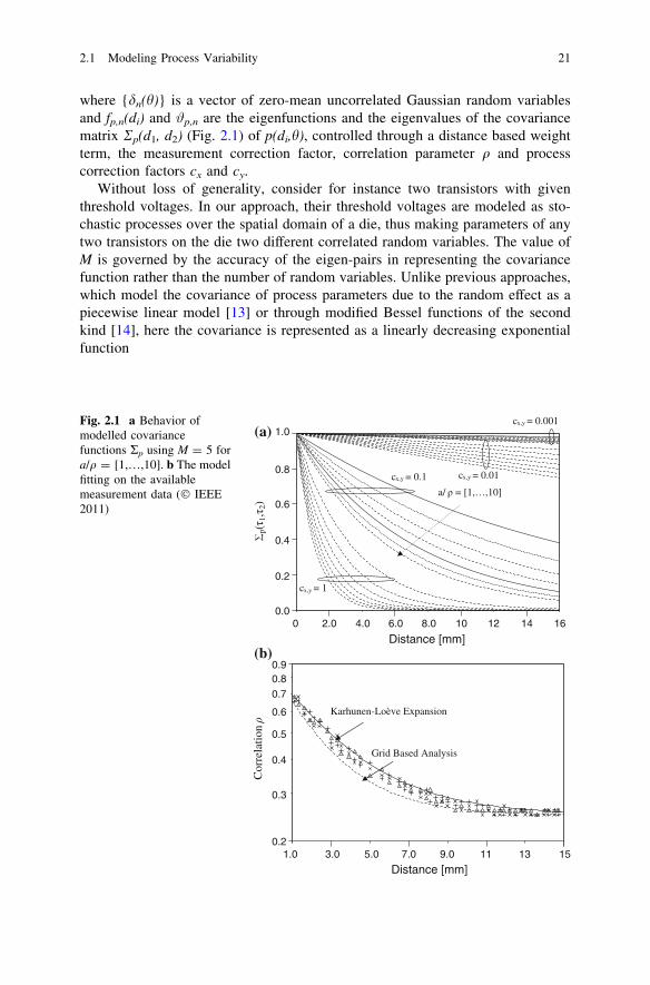
where {dn(h)} is a vector of zero-mean uncorrelated Gaussian random variablesand fp,n(di) and #p,n are the eigenfunctions and the eigenvalues of the covariancematrix Rp(d1, d2) (Fig. 2.1) of p(di,h), controlled through a distance based weightterm, the measurement correction factor, correlation parameter q and processcorrection factors cx and cy.
Without loss of generality, consider for instance two transistors with giventhreshold voltages. In our approach, their threshold voltages are modeled as sto-chastic processes over the spatial domain of a die, thus making parameters of anytwo transistors on the die two different correlated random variables. The value ofM is governed by the accuracy of the eigen-pairs in representing the covariancefunction rather than the number of random variables. Unlike previous approaches,which model the covariance of process parameters due to the random effect as apiecewise linear model [13] or through modified Bessel functions of the secondkind [14], here the covariance is represented as a linearly decreasing exponentialfunction
0.8
a/ = [1,…,10]
cx,y = 0.1
cx,y = 1
cx,y = 0.01
cx,y = 0.001
p(1,
2)
1.0
0.2
0.6
0.4
160 4.0 2.0 6.0 8.0 10 12 14 0.0
Distance [mm]
Distance [mm]
Cor
rela
tion
Karhunen-Loève Expansion
Grid Based Analysis
1.0 5.03.0 7.0 9.0 11 13 150.2
0.3
0.4
0.5
0.6
0.90.8
0.7
(a)
(b)
Fig. 2.1 a Behavior ofmodelled covariancefunctions Rp using M = 5 fora/q = [1,…,10]. b The modelfitting on the availablemeasurement data (� IEEE2011)
2.1 Modeling Process Variability 21

Cpðd1; d2Þ ¼ 1þ 1dx;y
� �� c � e�cx dx1�dx2j j�cy dy1�dy2j j=q
� �ð2:3Þ
where 1 is a distance based weight term, c is the measurement correction factor forthe two transistors located at Euclidian coordinates (x1, y1) and (x2, y2), respec-tively, cx and cy are process correction factors depending upon the processmaturity. For instance, in Fig. 2.1a, process correction factor cx,y = 0.001 relatesto a very mature process, while cx,y = 1 indicates that this is a process in a ramp upphase. The correlation parameter q reflecting the spatial scale of clustering definedin [-a, a] regulates the decaying rate of the correlation function with respect todistance (d1, d2) between the two transistors located at Euclidian coordinates (x1,y1) and (x2, y2).
Physically, lower a/q implies a highly correlated process and hence, a smallernumber of random variables are needed to represent the random process andcorrespondingly, a smaller number of terms in the Karhunen-Loève expansion.This means that for cx,y = 0.001 and a/q = 1 the number of, transistors that needto be sampled to assess, say a process parameter such as threshold voltage is muchless than the number that would be required for cx,y = 1 and a/q = 10 because ofthe high nonlinearity shown in the correlation function. To maintain a fixed dif-ference between the theoretical value and the truncated form, M has to beincreased when a increases at constant b.
In other words, for a given M, the accuracy decreases as a/b increases.Eigenvalues #p,n and eigenfunctions fp,n(s) are the solution of the homogeneousFredholm integral equation of the second kind indexed on a bounded domainD. To find the numerical solution of Fredholm integral, each eigenfunction isapproximated by a linear combination of a linearly decreasing exponential func-tion. Resulting approximation error is than minimized by the Galerkin method.One example of spatial correlation dependence and model fitting on the availablemeasurement data through Karhunen-Loève expansion is given in Fig. 2.1b. Forcomparison purposes, a grid-based spatial-correlation model is intuitively simpleand easy to use, yet, its limitations due to the inherent accuracy-versus-efficiencynecessitate a more flexible approach, especially at short to mid range distances[14]. We now introduce a model gp = f(.), accounting for voltage and currentshifts due to random manufacturing variations in transistor dimensions and processparameters defined as
gp ¼ f ðm;W�; L�; p�Þ ð2:4Þ
where m defines a fitting parameter estimated from the extracted data, W* and L*
represent the geometrical deformation due to manufacturing variations and p*
models electrical parameter deviations from their corresponding nominal values,e.g. altered transconductance, threshold voltage, etc. (Appendix A).
22 2 Random Process Variation in Deep-Submicron CMOS
2.2 Stochastic MNA for Process Variability Analysis
Device variability effects limitations are rudimentary issues for the robust circuitdesign and their evaluation has been subject of numerous studies. Several modelshave been suggested for device variability [15–17], and correspondingly, a numberof CAD tools for statistical circuit simulation [18–23]. In general, a circuit designis optimized for parametric yield so that the majority of manufactured circuitsmeet the performance specifications. The computational cost and complexity ofyield estimation, coupled with the iterative nature of the design process, makeyield maximization computationally prohibitive. As a result, circuit designs areverified using models corresponding to a set of worst-case conditions of the pro-cess parameters. Worst-case analysis refers to the process of determining thevalues of the process parameters in these worst-case conditions and the corre-sponding worst-case circuit performance values. Worst-case analysis is very effi-cient in terms of designer effort, and thus has become the most widely practicedtechnique for statistical analysis and verification. Algorithms previously proposedfor worst-case tolerance analysis fall into four major categories: corner technique,interval analysis, sensitivity-based vertex analysis and Monte Carlo simulation.
The most common approach is the corners technique. In this approach, eachprocess parameter value that leads to the worst performance is chosen indepen-dently. This method ignores the correlations among the processes parameters, andthe simultaneous setting of each process parameter to its extreme value result insimulation at the tails of the joint probability density of the process parameters.Thus, the worst-case performance values obtained are extremely pessimistic.Interval analysis is computationally efficient but leads to overestimated results, i.e.,the calculated response space enclose the actual response space, due to theintractable interval expansion caused by dependency among interval operands.Interval splitting techniques have been adopted to reduce the interval expansion,but at the expense of computational complexity. Traditional vertex analysisassumes that the worst case parameter sets are located at the vertices of parameterspace, thus the response space can be calculated by taking the union of circuitsimulation results at all possible vertices of parameter space. Given a circuit withM uncertain parameters, this will result in a 2M simulation problem. To furtherreduce the simulation complexity, sensitivity information computed at the nominalparameter condition is used to find the vertices that correspond to the worst casesof circuit response. The Monte Carlo algorithm takes random combinations ofvalues chosen from within the range of each process parameter and repeatedlyperforms circuit simulations. The result is an ensemble of responses from whichthe statistical characteristics are estimated. Unfortunately, if the number of itera-tions for the simulation is not very large, Monte Carlo simulation always under-estimates the tolerance window. Accurately determining the bounds on theresponse requires a large number of simulations, so consequently, the Monte Carlomethod becomes very cpu-time consuming if the chip becomes large. Otherapproaches for statistical analysis of variation-affected circuits, such as the one
2.2 Stochastic MNA for Process Variability Analysis 23

based on the Hermite polynomial chaos [24] or the response surface methodology,are able to perform much faster than a Monte Carlo method at the expense of adesign of an experiments preprocessing stage [25]. In this section, the circuits aredescribed as a set of stochastic differential equations and Gaussian closureapproximations are introduced to obtain a closed form of moment equations. Evenif a random variable is not strictly Gaussian, a second-order probabilistic char-acterization yields sufficient information for most practical problems.
Modern integrated circuits are often distinguished by a very high complexityand a very high packing density. The numerical simulation of such circuitsrequires modeling techniques that allow an automatic generation of networkequations. Furthermore, the number of independent network variables describingthe network should be as small as possible. Circuit models have to meet twocontradicting demands: they have to describe the physical behavior of a circuit ascorrect as possible while being simple enough to keep computing time reasonablysmall. The level of the models ranges from simple algebraic equations, overordinary and partial differential equations to Boltzmann and Schrodinger equationsdepending on the effects to be described. Due to the high number of networkelements (up to millions of elements) belonging to one circuit one is restricted torelatively simple models. In order to describe the physics as good as possible, socalled compact models represent the first choice in network simulation. Complexelements such as transistors are modeled by small circuits containing basic net-work elements described by algebraic and ordinary differential equations only. Thedevelopment of such replacement circuits forms its own research field and leadsnowadays to transistor models with more than five hundred parameters. A wellestablished approach to meet both demands to a certain extent is the description ofthe network by a graph with branches and nodes. Branch currents, branch voltagesand node potentials are introduced as variables. The node potentials are defined asvoltages with respect to one reference node, usually the ground node. The physicalbehavior of each network element is modeled by a relation between its branchcurrents and its branch voltages. In order to complete the network model, thetopology of the elements has to be taken into account. Assuming the electricalconnections between the circuit elements to be ideally conducting and the nodes tobe ideal and concentrated, the topology can be described by Kirchhoff’s laws (thesum of all branch currents entering a node equals zero and the sum of all branchvoltages in a loop equals zero). In general, for time-domain analysis, modifiednodal analysis (MNA) leads to a nonlinear ordinary differential equation or dif-ferential algebraic equation system which, in most cases, is transformed into anonlinear algebraic system by means of linear multistep integration methods[26, 27] and, at each integration step, a Newton-like method is used to solve thisnonlinear algebraic system (Appendix B). Therefore, from a numerical point ofview, the equations modeling a dynamic circuit are transformed to equivalentlinear equations at each iteration of the Newton method and at each time instant ofthe time-domain analysis. Thus, we can say that the time-domain analysis of anonlinear dynamic circuit consists of the successive solutions of many linear
24 2 Random Process Variation in Deep-Submicron CMOS
circuits approximating the original (nonlinear and dynamic) circuit at specificoperating points.
Consider a linear circuit with N ? 1 nodes and B voltage-controlled branches(two-terminal resistors, independent current sources, and voltage-controlledn-ports), the latter grouped in set B. We then introduce the source current vectori [ RB and the branch conductance matrix G [ RB9B. By assuming that thebranches (one for each port) are ordered element by element, the matrix is blockdiagonal: each 1 9 1 block corresponds to the conductance of a one-port and inany case is nonzero, while n 9 n blocks correspond to the conductance matrices ofvoltage-controlled n-ports. More in detail, the diagonal entries of the n 9 n blockscan be zero and, in this case, the nonzero off-diagonal entries, on the same row orcolumn, correspond to voltage-controlled current sources (VCCSs). Now, considerMNA and circuits embedding, besides voltage-controlled elements, independentvoltage sources, the remaining types of controlled sources and sources of processvariations.
We split the set of branches B in two complementary subsets: BV of voltage-controlled branches (v-branches) and BC of current-controlled branches (c-branches).
Conventional nodal analysis (NA) is extended to MNA [27] as follows: currentsof c-branches are added as further unknowns and the corresponding branchequations are appended to the NA system. The N 9 B incidence matrix A can bepartitioned as A = [Av Ac], with Av [ RN9Bv and Ac [ RN9Bc. As in conventionalNA, constitutive relations of v-branches are written, using the conductancesubmatrix G [ RBc9Bv in the form
iv ¼ Gvv ð2:5Þ
while the characteristics of the c-branches, including independent voltage sourcesand controlled sources except VCCSs, are represented by the implicit equation
Bcvc þ Rcic þ vc þ Fcg ¼ 0 ð2:6Þ
where Bc, Rc, Fc [ RBc9Bc, vc = (ATvc) [ RBc [26] and g [ RBc is a random vectoraccounting for device variations as defined in (2.4). These definitions are inagreement with those adopted in the currently used simulators and suffice for alarge variety of circuits. Note that from the practical use perspective, a user mayonly be interested in voltage variations over a period of time or in the worst case ina period of time. This information can be obtained once the variations in any giventime instance are known. By using the above notations, (2.5) and (2.6) can bewritten in the compact form as
Fðq0; q; tÞ þ Bðq; tÞ � g ¼ 0 ð2:7Þ
where q ¼ vc iv½ ffiT is the vector of stochastic processes which represents the statevariables (e.g. node voltages) of the circuit and g is a vector of wide-sense sta-tionary processes. B(q, t) is an N 9 Bc matrix, the entries of which are functions ofthe state q and possibly t. Every column of B(q, t) corresponds to g, and has
2.2 Stochastic MNA for Process Variability Analysis 25

normally either one or two nonzero entries. The rows correspond to either a nodeequation or a branch equation of an inductor or a voltage source. Equation (2.7)represents a system of nonlinear stochastic differential equations, which formulatea system of stochastic algebraic and differential equations that describe thedynamics of the nonlinear circuit that lead to the MNA equations when the randomsources g are set to zero. Solving (2.7) means to determine the probability densityfunction P of the random vector q(t) at each time instant t. Formally the probabilitydensity of the random variable q is given as
PðqÞ ¼ jCðqÞjNðh�1ðqÞjm;RÞ ð2:8Þ
where |C(q)| is the determinant of the Jacobian matrix of the inverse transformh-1(q) with h a nonlinear function of g. However, generally it is not possible tohandle this distribution directly since it is non-Gaussian for all but linearh. Therefore it may be convenient to look for an approximation which can befound after partitioning the space of the stochastic source variables g in a givennumber of subdomains, and then solving the equation in each subdomain by meansof a piecewise-linear truncated Taylor approximation. If the subdomains are smallenough to consider the equation as linear in the range of variability of g, or that thenonlinearities in the subdomains are so smooth that they might be considered aslinear even for a wide range of g, it is then possible to combine the partial resultsand obtain the desired approximated solution to the original problem.
Let x0 = x(g0, t) be the generic point around which to linearize, and with the
change of variable n = x - x0 = ½ðq� p0ÞT ; ðg� g0ÞT ffiT , the first-order Taylorpiecewise-linearization of (2.7) in x0 yields
Pðx0Þn0 þ ðKðx0Þ þ P0ðx0ÞÞn ¼ 0 ð2:9Þ
where K(x) = B0(x), P(x) = F0(x). Transient analysis requires only the solution ofthe deterministic version of (2.7), e.g. by means of a conventional circuit simu-lator, and of (2.9) with a method capable of dealing with linear stochastic dif-ferential equations with stochasticity that enters only through the initial conditions.Since (2.9) is a linear homogeneous equation in n, its solution, will always beproportional to g - g0. We can rewrite (2.9) as
n0ðx0Þ ¼ Eðx0Þn0 þ Fðx0Þg0 ð2:10Þ
Equation (2.10) is a system of stochastic differential equations which is linear inthe narrow sense (right-hand side is linear in n and the coefficient matrix for thevector of variation sources is independent of n) [28]. Since these stochastic pro-cesses have regular properties, they can be considered as a family of classicalproblems for the individual sample paths and be treated with the classical methodsof the theory of linear stochastic differential equations. By expanding every ele-ment of n(t) with
26 2 Random Process Variation in Deep-Submicron CMOS

niðtÞ ¼ CðtÞðg� g0Þ ¼Xm
j¼1
aijðtÞ�gj ð2:11Þ
for m elements of a vector g. As long as aj(t) is obtained, the expression for n(t) isknown, so that the covariance matrix of the solution can be written as
Rnn ¼ CRggCT ð2:12Þ
Defining aj tð Þ ¼ a1j; a2j; . . .; anj
� �T, Fj tð Þ ¼ F1j;F2j; . . .;Fnj
� �T, the require-
ment for a(t) is
a0jðtÞ ¼ EðtÞaj þ FðtÞ ð2:13Þ
Equation (2.13) is an ordinary differential equation, which can be solved by afast numerical method.
2.3 Statistical Timing Analysis
Statistical static timing analysis is a potential alternative to predict the timinguncertainty due to the random process variation. In addition to the problem offinding the delay of the circuit, it is also key to improve this delay when the timingrequirements are not met. Hence, deterministic STA (DSTA) methods typicallyreport the slack at each node in the circuit, in addition to the circuit delay andcritical paths. The slack of a node is the difference between the latest time a signalcan arrive at that node, such that the timing constraints of the circuit are satisfied(referred to as the required time), and the actual latest arrival time of the signal atthat node. Similar to the circuit delay, the slack of a node is a random variable inthe SSTA formulation. Third problem associated with STA methods is latch-basedsequential timing analysis, which involves multiple-phase clocks, clock-scheduleverification, etc. The statistical formulation of timing analysis introduces severalnew modeling and algorithmic issues such as: topological correlation, spatialcorrelation and non-normal process parameters and nonlinear delay models.
Normal or Gaussian distributions are found to be the most commonly observeddistributions for random variations, and a number of elegant analytical results existfor them in the statistics literature. However, some physical device parametersmay have significantly non-normal distributions. An example of a non-normaldevice parameter is gate length due to the variation in depth of focus. Even if thephysical device parameters are indeed normally distributed (e.g., doping concen-tration has a normal distribution), the dependence of the electrical deviceparameters and gate delay on these physical parameters may not be linear, givingrise to non-normal gate delays. With reduction of geometries, process variation isbecoming more pronounced, and the linear approximation may not be accurate forsome parameters.
2.2 Stochastic MNA for Process Variability Analysis 27
Typically, there are two types of SSTA techniques: Monte Carlo methods andprobabilistic analysis methods. In contrast to Monte Carlo based methods, whichare based on sample-space enumeration, probabilistic methods explicitly modelgate delay and arrival times with random variations. These methods typicallypropagate arrival times through the timing graph by performing statistical sum andmaximum operations. They can be classified into two broad classes: path-basedapproaches and block-based approaches. In path-based SSTA algorithms, a set ofpaths, which is likely to become critical, is identified, and a statistical analysis isperformed over these paths to approximate the circuit-delay distribution. The basicadvantage of this approach is that the analysis is split into two parts—the com-putation of path delays followed by the statistical maximum operation over thesepath delays. However, the difficulty with the approach is how to rigorously find asubset of candidate paths such that no path that has significant probability of beingcritical in the parameter space is excluded. In addition, for balanced circuits, thenumber of paths that must be considered can be very high. On the other hand, theblock-based methods follow the DSTA algorithm more closely and traversethe circuit graph in a topological manner.
In both block-based and path-based SSTA approaches, the gate timing modelsplay a significant role for the accuracy-efficiency trade-off. In function-basedSSTA the gate delay is modeled as a linear or non-linear function [29] of processvariations, similar to the traditional non-linear delay model [30] in STA. Thecoefficients are characterized and stored in look-up tables with input slew (Sin) andload effective capacitance (Ceff) as parameters. When calculating statistical gatedelay moments, these coefficients are interpolated based on the nominal value ofSin and Ceff. However, due to process variations, both Sin and Ceff are variational aswell. Not considering the statistical nature of Sin and Ceff can result in 30 % delayerrors [31]. Also, similar to non-linear delay model, function-based models do notaccount for resistive interconnect loads and nonlinear input waveforms. Addi-tionally, the function-based delay representation is entirely based on non-physicalor empirical models, which is their major source of inaccuracy [32].
A large number of more physical gate timing models have been proposed foraccurate STA, such as voltage-dependent current source models [31–39] andtransistor-level gate models [40–48]. These gate timing models, denoted as volt-age-input voltage-output gate models, represent every gate by current sources andcapacitances with respect to input voltage (Vi) and output voltage (Vo). Mostvoltage-dependent current source models target only accurate modeling of com-binational gate delay with the assumptions of single input switching and that theinput signal is independent of the output signal. Hence, they fail to model internalnodes and capacitances, which lead to different undesired symptoms for sequentialelements, including non-monotonic behavior, failure to model storage behavior,etc. [37]. In contrast, the transistor-level gate models can handle sequential circuitsin the same way as the combinational circuits without the limiting assumptions ofcurrent source models and are able to consider multiple input (near-)simultaneousswitching (MISS). Additionally, the transistor-level gate models have a betterdefined physical relationship with node voltages and physical parameters and are
28 2 Random Process Variation in Deep-Submicron CMOS
more general and accurate for timing, noise and power analysis and practical formulti-million gate STA runs [40–48]. The transistor-level gate models are utilizedto estimate the timing variabilities based on corner-based timing analysis in [44].However, these methods do not take signal correlations and sequential cells intoconsideration, and most of them are just verified in several simple single gatesconsidering only single input switching. Additionally, the solvers proposed forthese statistical delay calculations either have difficulties for other gate timingmodels [32, 33] or require many simulation trails [31, 34, 44].
In this section, we present a novel method to extend voltage-based gate modelsfor statistical timing analysis. Correlations among input signals and between inputsignal and delay are preserved during simulation by using same model format forthe voltage and all elements in gate models. In the statistical solver, all inputsignals and their correlations are considered together, thus fundamentallyaddressing MISS in statistical timing analysis. The variational waveform for sta-tistical delay calculation is computed with random differential equation-basedmethod. For high accuracy in the case of large process variations, the statisticalsolver divides the process variation space into several sub-spaces and performs thestatistical timing analysis in each sub-space. Since a common format for voltageand current waveforms and passive components (resistances and capacitances) isutilized in the gate models, the correlations among input signals and between inputsignal and delay are preserved during statistical delay calculation. Furthermore,since described timing analysis is based on the transistor-level gate models, it isable to handle both combinational and sequential circuits.
2.3.1 Statistical Simplified Transistor Model
In transistor-level gate models [40–45, 47, 48], the transistor model needs tocapture sufficient second-order effects for accuracy, accounting for the impact ofprocess variations, while still being simple enough to be evaluated efficiently. Thetransistor model for timing analysis in [48] uses look-up tables for drain-sourcecurrent and an input-transition dependent constant value for five intrinsic capac-itances of each transistor. The look-up table based transistor models in [41, 44, 45]implement SPICE’s model version for the five intrinsic capacitances. If linear-centric method is utilized, in which the Jacobian matrix is constant for all itera-tions, the efficiency of transistor-level timing analysis is significantly improved[41, 44, 45, 47]. Current source models require transient analysis or ac analysis fordifferent combinations of Sin and Ceff or different combinations of input and outputvoltages at different corners. For transistor-level gate modeling, only character-ization of the unique transistors in the standard cell library is needed. The currentand capacitances of SSTM are obtained by a dc sweep at the gate, drain and sourceterminals. For statistical analysis, the sensitivities in SSTM are characterized by afinite-difference approximation.
2.3 Statistical Timing Analysis 29
CMOS transistor drain current modeling: Generally, the MOS transistor draincurrent IDS is modeled by compact models like BSIM4. With several hundredprocess parameters, BSIM3/4 determines drain current and sixteen intrinsiccapacitances by solving complex equations, which are functions of the processparameters in the model. The physical properties are accurately represented bythose parameters, however, the huge amount of computation time makes itimpractical for fast timing analysis.
Avoiding approximating data to expressions, the model described in this sectionaddresses these issues by directly using measured or simulated data. Moreover, incomparison with advanced analytical models, this table-based model gains sig-nificant speed advantage by using the efficient interpolation and extrapolationmethods and resourceful implementation of look-up table sizes.
In nanometer technology, VT is not only a function of VBS but also VDS, whichimplies that a 2D look-up table for IDS with entries VDS and VGS - VT is notpractical. The IDS(VGS,VDS) characteristics have almost the same shape underdifferent VBS when VBS is not close to the supply voltage, implying a possibility ofreducing data points corresponding to VBS. For constant VBS, IDS displays differentnonlinearity in three operating regions. In the linear region, the current IDS increaserapidly along with VDS while shows nearly linear dependence on VDS with rela-tively much slower slope in the saturation region. In the cutoff region, however,the current is close to zero and shows a weak relationship with VDS and VGS. In[49], a continuous piecewise linear surface is generated for the current curve usingtrilinear interpolation [50], mainly due to its reduced complexity in comparisonwith explicit model evaluation and monotonic piecewise cubic interpolation [51]or spline cubic Hermit interpolation [52]. If derivative of the current is not con-tinuous, Broyden’s method [49] avoids the derivative calculation at every iterationby replacing it with finite difference approximation.
Transistor capacitance modeling: The transient response of a combinationallogic gate is sensitive to the transistor intrinsic capacitances in the gate. If theintrinsic capacitances are not modeled accurately, the error introduced can accu-mulate when the transient pulse propagates through the logic chain. Gate levelmodels model a gate capacitance to a constant value Ceff ignoring the nonlinearproperty of the intrinsic capacitances hidden in the gate. One way to modelnonlinear intrinsic capacitances is to represent them as voltage-dependent terminalcharge sources as in BSIM4. The sixteen capacitances of a transistor are computedfrom the charge Q by Cij = qQi/qVj at every time step, where i and j denote thetransistor terminals. Although this method may be the most accurate by means ofsophisticated charge formulations, the performance and characterization runtimeposes the complexity challenges for S/STA.
In the 45 nm node and beyond, the intrinsic capacitance becomes increasinglynonlinear. In order to accurately capture the capacitances, analytical models stillplay a dominant role in transistor-level timing analysis [44, 45, 50, 53–55]. In [48],the constant capacitance values based on the initial state (cutoff or linear state) areused for the entire transition. However, the assumption that the capacitancesinfluence the output waveform mostly at the beginning would result in deviations
30 2 Random Process Variation in Deep-Submicron CMOS
at the end of the transition, adding errors for output slew due to the strongcapacitance nonlinearity. In order to improve accuracy while still maintainingsatisfactory computational efficiency, the model in [49] treats the five capacitancesdifferently. The gate capacitances CGS, CGD and CGB use 2D look-up tables (as afunction of VGS and VDS), while constant values are characterized for junctioncapacitances CSB and CDB. CSB is at least one order of magnitude smaller than theother capacitances, and normally, CDB is negligible compared to output load. As aconsequence, using constant values for CSB and CDB promises fast performancewithout accuracy loss.
Statistical extension: In addition to the nominal values for the dc current sourceand intrinsic capacitances, the statistical extension of the model contains thesensitivities of these model elements to any statistical parameter of interest.
The statistical description of the current and the intrinsic capacitance in themodel are evaluated as IDS(Dp) = IDS,nom ? dIDS(Dp) and Cj(Dp) = Cj0 ? dCj(Dp),where p is the random parameter, which is the sum of nominal value pkq andrandom variable g with zero mean l and standard deviation r. These processparameters can be physical process parameters such as effective channel length Leff,and threshold voltage VT, or non-physical parameters derived from dimension-reduction methods, such as principal component analysis, independent componentanalysis [56, 57], and reduced rank reduction [58]. Dp is the parameter deviationfrom the nominal value p0 sampled from g and Cjq is the nominal value of the jthcapacitance. Note that the correlations among the statistical variables are submis-sive to accuracy-speed trade-off. The numerical sensitivity is characterized byperturbing the statistical parameter being modeled above and below (e.g. ±r) itsnominal value. Since nowadays standard cell libraries consist of hundreds of cellswith many process corners, gate level models require a significant amount of cputime to characterize all the standard cells. The described transistor-level gate modelhas modest characterization requirements: it only needs to characterize the uniquetransistors in the cell library. It is also worth mentioning that IDS and the gatecapacitances are roughly proportional to W/L and WL, respectively, raising thepossibility to require only a few table models for each MOST type.
2.3.2 Bounds on Statistical Delay
The process variation vector g includes both global process variations and localvariations. For a specific random process parameter with a global deviation andlocal deviations, the global deviation and correlated local deviation affect all thetransistors in the same way hence they can be clubbed together [59]. The largenumber of local process deviations can be significantly reduced to a much smallernumber of independent local variables with techniques like principal componentanalysis. According to [48, 59], the local variables can be further collapsed to asingle variable by treating it as in a root of the sum of square technique. Forvoltage-input voltage-output gate models, like current source models and
2.3 Statistical Timing Analysis 31
transistor-level gate models in [31–34, 40–48], nodal analysis or modified nodalanalysis is used for gate simulation. Rewriting (2.7) as
Fðq0; q; t; gÞ ¼ 0 ð2:14Þ
the first-order Taylor piecewise-linearization of (2.14) in x0 yields
Pðx0Þn0 ¼ Kðx0Þnþ Lðx0Þg ð2:15Þ
where P, K and L are matrices defined as qF/qx00, qF/qx0, qF/qp, respectively.Transient analysis requires only the solution of the deterministic version of (2.14),e.g. by means of a conventional circuit simulator, and of (2.15) with a methodcapable of dealing with linear stochastic differential equations with stochasticitythat enters only through the initial conditions. Since (2.15) is a linear homogeneousequation in n, its solution, will always be proportional to g - g0. According to[60], (2.8) has a unique mean square solution which can be represented byn(t) = C(t)(g – g0). Following the procedure as described in Sect. 2.2, (2.15) forC(t) can be written as
Pðx0ÞC0ðtÞ ¼ Kðx0ÞCðtÞ þ Lðx0Þ ð2:16Þ
In delay distribution calculation, at every time point, P, K and L are updated andfunction (2.16) can be solved to obtain C(t). If C(t) and L have high dimension(e.g. number of process variations is large), the sensitivity of the variationalvoltage to the jth process variation, must be computed. Based on (2.16), Cj(t) iscalculated as
Pðx0ÞC0jðtÞ ¼ Kðx0ÞCjðtÞ þ Lðx0Þu j ¼ 1 : pm ð2:17Þ
where u is selection vector whose elements are all zeros except the jth element,which has value one. After using a numerical integration method, due to xo-dependent coefficients P(x0), K(x0) and L(x0), (2.17) becomes a linear algebraicequation with respect to the variable Cj(t). The covariance matrix (2.11) of thesolution, rewritten here for clarity, is expressed as
Rnn ¼ CRggCT ð2:18Þ
To extend voltage-input voltage-output gate models for statistical timinganalysis, in addition to statistical simulation, the extraction of statistical delay fromvariational voltages is also necessity. The extraction methods of existing gate levelstatistical timing analysis have the three main categories: interpolation-basedanalysis, Monte Carlo simulation based on statistical current source models anddirect calculation based on Markovian process assumption. In interpolation-basedanalysis [44] the output waveforms at different corners are simulated, and then theoutput waveform is characterized by linear interpolation. However, this methodassumes that the results at different corners are linear with respect to the processvariations and large number of samples is required for delay calculation. Thestatistical moments of several crossing times are calculated by Monte Carlo
32 2 Random Process Variation in Deep-Submicron CMOS

simulations based on statistical current source models in [31, 34]. However, eventhough the Monte Carlo simulations are applied, the accuracy of statistical delaycalculation is not competitive due to the over-simplified current source models. Indirect calculation based on Markovian process assumption, the delay distribution iscalculated by assuming that the voltage at every time point is a Markovian sto-chastic process due to the numerical integration method [32, 61, 62]. In order tocalculate the distribution of a crossing time, the joint probability of voltage atdifferent time steps is calculated by using the bivariate normal distribution, whichis erroneous when the Gaussian distribution assumption for voltages is inaccurate.Here, the boundaries of voltage of interest, which needs to be stored and propa-gated (denoted as Nr with mean value lNr)), can be expressed as
½Nr;min;Nr;maxffi ¼ lNr�X
k
X
m
Rnnj jmaxf g ð2:19Þ
for any pi [ {p1,…,pm} of i [ {i1,…,ik} transistors connected to node r [ {r1,…,rq}.In this scheme higher order moments are expressed in terms of the first and secondorder moments as if the components of Nr are Gaussian processes. The method isfast, and comparable to regular nominal circuit simulation. Suppose that there arem-trial Monte Carlo simulation for n faults, the method (using statistical data of theprocess parameters variations) gains a theoretical speed-up of m9n over the MonteCarlo method. During path-based timing analysis, each critical path can be sim-ulated as a whole to obtain lNr and Nr directly for statistical path delay calculation.Gate-by-gate propagation can also be used. For a single transition propagatingfrom gate to gate, lNr and Nr of each gate during the transition period (when lNr
switches from low to high or from high to low) are propagated. This expresses thevoltages as linear functions of the process variables, through which the correla-tions between voltages are implicitly defined. During statistical timing analysis,the correlation of signals caused by process variations and path re-convergenceshould be considered and efficiently simulated.
Here, if more than one input switch in a multi-input gate, the 50 % crossingtime standard deviation r of every two switching inputs are calculated andchecked. If the signals are not overlapping, the correlation between them will beignored and the latest/earliest input or inputs will be propagated while the other isassumed static. On the other hand, if they are overlapping, all stochastic correlatedinputs are considered.
2.3.3 Reducing Computational Complexity
The gate models are constructed by replacing every transistor in the gate by itscorresponding SSTM. After RC extraction, model order reduction (MOR) tech-niques is employed to reduce the complexity of the interconnect model, in whichevery resistance and capacitance is represented as a linear function of process
2.3 Statistical Timing Analysis 33
variations. In an asymptotic waveform evaluation (AWE) algorithm [63] explicitmoment matching was used to compute the dominant poles via Padé approxi-mation. As the AWE method is numerically unstable for higher-order momentapproximation, a more elegant solution to the numerical problem of AWE is to useprojection-based MOR methods. In the Padé via Lanczos (PVL) method [64], theLanczos process, which is a numerically stable method for computing eigenvaluesof a matrix, was used to compute the Krylov subspace. In PRIMA [65] the Krylovsubspace vectors are used to form the projector for the congruence transformation,which leads to passive models with the matched moments in the rationalapproximation paradigm. However, these methods are not efficient for circuitswith many inputs and output terminals as the reducing cost are tied to the numberof terminals; the number of poles of reduced models is also proportional to thenumber of terminals. Additionally, PRIMA-like methods do not preserve structureproperties like reciprocity of a network.
Another approach to circuit-complexity reduction is to reduce the number ofnodes in the circuits and approximate the newly added elements in the circuit matrixin reduced rational forms by approximate Gaussian elimination for RC circuits [66].Alternatively, model order reduction can be performed by means of singular-value-decomposition (SVD) based approaches such as control-theoretical-based truncatedbalance realization (TBR) methods, where the weakly uncontrollable and unob-servable state variables are truncated to achieve the reduced models [67–73]. Themajor advantage of SVD-based approaches over Krylov subspace methods lies intheir ability to ensure the errors satisfying an a priori upper bound [71]. Also, SVD-based methods typically lead to optimal or near optimal reduction results as theerrors are controlled in a global way, although, for large scale problems, iterativemethods have to be used to find an adequate balanced approximation (truncation).In this respect, ideas based on balanced reduction methods are significant since theyoffer the possibility to perform order selection during the computation of the pro-jection spaces and not in advance. Typically in balanced reduction methods, there isa rapid decay in the Gramians eigenvalues. As a consequence these Gramians canbe well approximated using low-rank approximations, which are used instead of theoriginal. Accordingly, several SVD approaches approximate the dominant Chole-sky factors (dominant eigensubspaces) of controllability and observability Gra-mians [68, 72, 73] to compute the reduced model.
In this section, we adjust the dominant subspaces projection model reduction(DSPMR) [68] and provide an approximate balancing transformation for circuitswhose coefficient matrices are large and sparse such as in interconnect. Theapproach presented here produces orthogonal basis sets for the dominant singularsubspace of the controllability and observability Gramians significantly reducingthe complexity and computational costs of singular value decomposition, whilepreserving model order reduction accuracy and the quality of the approximationsof the TBR procedure.
In the analysis of delay or noise in on-chip interconnect we study the propa-gation of signals in the wires that connect logic gates. These wires may have
34 2 Random Process Variation in Deep-Submicron CMOS
numerous features: bends, crossings, vias, etc., and are modeled by circuitextractors in terms of a large number of connected circuit elements: capacitors,resistors and more recently inductors. Given a state-space formulation of theinterconnect model
Cðdx=dtÞ ¼ GxðtÞ þ BuðtÞyðtÞ ¼ ET xðtÞ
ð2:20Þ
where C, G [ Rn9n are matrices describing the reactive and dissipative parts of theinterconnect, respectively, B [ Rn9p is a matrix that defines the input ports, E [Rp9n is matrix that defines the outputs, and y(t) [ Rq and u(t) [ Rp, are the vectorsof outputs and inputs, respectively, the model reduction algorithm seek to producea similar system
C_
dx_=dt ¼ G
_
x_ðtÞ þ B
_
uðtÞ
y_ðtÞ ¼ E
_Tx_ðtÞ
ð2:21Þ
where C_
;G_
[ Rk9k, B_
[ Rk9m, E_
[ Rp9k, of order k much smaller than the original
order n, but for which the outputs y(t) and y_(t) are approximately equal for inputs
u(t) of interest. The Laplace transforms of the input output transfer functions
HðsÞ ¼ ETðGþ sCÞ�1B
H_
ðsÞ ¼ E_TðG_
þ sC_
Þ�1B_
ð2:22Þ
are used as a metric for approximation accuracy if
HðsÞ � H_
ðsÞ���
���\ e ð2:23Þ
for a given allowable error e and an allowed domain of the complex frequencyvariable s, the reduced model is accepted as accurate.
Balanced truncation [67, 73], singular perturbation approximation [74], andfrequency weighted balanced truncation [75] are model reduction methods forstable systems. Except for modal truncation each of the above methods is basedeither explicitly or implicitly on balanced realizations, the computation of whichinvolves the solutions of Lyapunov equations
GXCT þ CXGT ¼ �BBT
GT YC þ CT YG ¼ �ET Eð2:24Þ
where the solution matrices X and Y are controllability and observability Grami-ans. The original implementation of balanced truncation [67] involves the explicitbalancing of the realization (2.20). This procedure is dangerous from the numericalpoint of view because the balancing transformation matrix T tends to be highly ill-conditioned. The square root method [73] is an attempt to cope with this problem
2.3 Statistical Timing Analysis 35
by avoiding explicit balancing of the system. The method is based on the Choleskyfactors of the Gramians instead of the Gramians themselves. In [76] the use of theHammarling method was proposed to compute these factors. Recently, in [68] and[72] it has been observed that solutions to Lyapunov equations often have lownumerical rank, which means that there is a rapid decay in the eigenvalues of theGramians.
Indeed, the idea of low-rank methods is to take advantage of this low-rankstructure to obtain approximate solutions in a low-rank factored form. The prin-cipal outcome of these approaches is that the complexity and the storage arereduced from O(N3) flops and O(N2) words of memory to O(N2r) flops and O(Nr)words of memory, respectively, where r is the approximate rank of the Gramian(r « N). Moreover, approximating the Cholesky factors of the Gramians directlyand using these approximations to provide a reduced model, has a comparable costto that of the popular moment matching methods. It requires only matrix-vectorproducts and linear solvers.
For large systems with a structured transition matrix, this method is anattractive alternative because the Hammarling method can generally not benefitfrom such structures. In the original implementation this step is the computation ofexact Cholesky factors, which may have full rank. We formally replace these(exact) factors by (approximating) low rank Cholesky factors [68, 72]. The iter-ative procedure approximates the low rank Cholesky factors ZX and ZY with rX,rY « n, such that ZXZH
X � X and ZY ZHY � Y , where H is Hermitian (complex-
conjugate) matrix. Note that the number of iteration steps imax needs not be fixed apriori. However, if the Lyapunov equation should be solved as accurate as pos-sible, correct results are usually achieved for low values of stopping criteria thatare slightly larger than the machine precision. Let
ZHY ZX ¼ UYRUH
X ð2:25Þ
be SVD of ZHY ZX of dimension N 9 m. The cost of this decomposition including
the construction of U is 14Nm2 ? O(m3) [77]. To avoid this, we perform eigen-value decomposition
ðZHY ZXÞHZH
Y ZX ¼ UYKUHX ð2:26Þ
Comparing (2.26) with (2.25) shows that the same matrix UX is constructed andthat
ðZHY ZXUXÞHZH
Y ZXUY ¼ K ¼ RHR ð2:27Þ
This algorithm requires Nm2 operations to construct ðZHY ZXÞH ZH
Y ZX andNmn ? O(m3) operations to obtain ZH
Y ZXUXR�1 for n 9 n R. The balancingtransformation matrix T is used to define the matrices SX = T(1:k) and SY ¼ T�T
ð1:kÞ.
If rk = rk+1, the reduced order realization is minimal, stable, and balanced, andits Gramians are equal to diag(r1,…,rk). The balancing transformation matrix canbe obtained as
36 2 Random Process Variation in Deep-Submicron CMOS

SX ¼ ZXUXR�1=2 SY ¼ ZY UYR�1=2 ð2:28Þ
then, under a similarity transformation of the state-space model, both parts can betreated simultaneously after a transformation of the system (C, G, B, E) with anonsingular matrix T [ Rn9n into a balanced system
C_
¼ SXCSHY G
_
¼ SXGSHY B
_
¼ SHY B E
_
¼ ESX ð2:29Þ
In this algorithm we assume that k B r (rank ZHY ZX). Note that SVDs are
arranged so that the diagonal matrix containing the singular values has the samedimensions as the factorized matrix and the singular values appear in non-increasing order.
2.4 Yield Constrained Energy Optimization
One of the most notable features of ultra-low power nanometer-scale CMOScircuits is the increased sensitivity of circuit performance to process parametervariation when operating at reduced VDD supplies. The growth of variability can beattributed to multiple factors, including the difficulty of manufacturing control, theemergence of new systematic variation-generating mechanisms, and mostimportantly, the increase in fundamental atomic-scale randomness, such as thevariation in the number of dopants in the transistor channel [5]. As a consequence,device upsizing may be required to achieve operational robustness against processvariability at the expense of a higher energy consumption and larger area occu-pation [6]. Technology scaling, circuit topologies, and architecture trends have allaligned to specifically target low-power trade-offs through the use of fine-grainedparallelism [7], near-threshold design [8], VDD scaling and body biasing [9].Similarly, a cross-layer optimization strategy is devised for variation resilience, astrategy that spans from the lowest level of process and device engineering to theupper level of system architecture. As a result, power-management has evolvedfrom static custom-hardware optimization to highly dynamic run-time monitoring,assessing, and adapting of hardware performance and energy with preciseawareness of the instantaneous application demands. These mechanisms allow todynamically select the most appropriate operating point for a particular processcorner that affects the die and its sub-components. Simultaneous circuit yield andenergy optimization with key parameters (supply voltage VDD and supply tothreshold voltage ratio VDD/VT) is a part of a system-wide strategy, where criticalparameters that minimize energy (e.g. VDD/VT) provide control mechanisms (e.g.adaptive voltage scaling) to run-time system. Yield constrained energy optimi-zation, as an active design strategy to counteract process variation in sub-thresholdor near-threshold operation, necessitates the need for statistical design paradigm toovercome the limitations of deterministic optimization schemes, such as sizing[78] and dual-VT allocation [79]. Analytical optimization based on sensitivities
2.3 Statistical Timing Analysis 37

[80], fitted [81] and physical [82] parameters offer guidelines for optimum poweroperation. The choice of the nonlinear optimization techniques [83–85] is based onthe nonlinear relationships that exist between device lengths and widths and theirassociated delays, particularly with strong short-channel effects in the nanometerregion, and leakage power.
In this section, we extend nonlinear optimization by developing a yield con-strained sequential energy minimization framework that is applied to multivariableoptimization in body bias enabled subthreshold and near-threshold designs. Thepresence of the yield constraint in nonlinear optimization makes the problem non-convex, thus hard to solve in general. In the proposed algorithm, we create asequence of minimizations of the feasible region with iteratively-generated low-dimensional subspaces. As the resulting sub-problems are small, global optimi-zation in both convex and non-convex cases is possible. The method can be usedwith any variability model, and is not restricted to any particular performanceconstraint. The yield constraint becomes active as the optimization concludes,eliminating the problem of overdesign in worst-case approach.
2.4.1 Optimum Energy Point
The optimum energy point arises from opposing trends in the dynamic and theleakage energy consumed per clock cycle as supply voltage VDD scales down. Thedynamic (CV2) energy decreases quadratically, but in the subthreshold region, theleakage energy per cycle increases as a result of the leakage energy being inte-grated over exponentially longer clock periods. With process scaling, the shrinkingof feature sizes implies smaller switching capacitances and thus lower dynamicenergy consumed. At the same time, leakage current in recent technology gener-ations have increased substantially, in part due to threshold voltage VT beingdecreased to maintain performance while the nominal supply voltage is scaleddown. On a chip-level, energy consumption is optimized by adjusting VDD
(dynamic supply voltage scaling) and VT (body-biasing) within its functionaloperating region (defined by its local process variations, i.e. the distributions of thecritical dimension size, oxide thickness, and threshold voltage). The mean value ofthe performance range at a particular temperature or voltage is determined by thesemiconductor process corner—an aggregation of process variations effects—thatimpacts the circuit. The range width is determined by process, voltage and tem-perature variations, which impose VDD to VT ratio, noise margins and thus limit theperformance range. Consider the delay dj of path j,
dj ¼ VDD
X
i2j
ðCintr;i þ x�1i Cextr;iÞI�1
drive;iekiVBB Tclk 8j 2 K ð2:30Þ
where i is an index that runs over all gates in the circuit, j is an index that runs overall circuit paths, K is the collection of all paths in the circuit, x is the gate sizing
38 2 Random Process Variation in Deep-Submicron CMOS
factor (x C 1), Cintr and Cextr are the switching intrinsic and extrinsic capacitanceof a gate, respectively, Idrive is the current drive of a gate, VBB represents thesymmetrical forward body-bias voltage (VBB = VDD - Vnwell = Vpwell), Tclk is theoperating clock period and k is fitting parameter. Expression (2.30) constrainsthe delay of each circuit path to be less than the targeted clock period, Tclk. Thedependence of Cintr,i on body-bias is accounted for through fitting parameter ki.Based on the above model, the total energy of a CMOS digital circuit design underbody-bias conditions is modeled as [86]
Etotal ¼ VDD
XN
i¼1
axiCintr;i
ð1� m1VBBÞm2Cextr;i
� VDD
þ TckxiIleak;i el1iVBB þ l2i el1iVBB � 1� �� �
0B@
1CA 8VBB 0 ð2:31Þ
where a is the average circuit activity factor, N is the total number of gates in thecircuits, and l1, l2, l3, m1 and m2 are fitting parameters. At a given VDD, the lowestenergy design is obtained when no gates are up-sized, e.g. xi = 1 8 gatesi. However, this also leads to the slowest design, as can be inferred from (2.30).We model the manufactured values of the parameters pk [ {p1,…,pm} for transistork as a random variable
pk ¼ lp;k þ rpðkkÞ � pðkk; hÞ ð2:32Þ
where lp,k and rp(kk) are the mean value and standard deviation of the parameterpk, (e.g. channel-length L, threshold voltage VT) respectively, p(kk,h) is the sto-chastic process corresponding to parameter p, kk denotes the location of transistork on the die with respect to a point origin and h is the die on which the transistorlies. Assuming that pk is a zero-mean Gaussian process and using the Karhunen-Loève expansion, pk can be written in truncated form (for practical implementa-tion) by a finite number of terms W as in Sect. 2.1 [87]
pk ¼ lp;k þ rpðkkÞ �XW
n¼1
ffiffiffiffiffiffiffiffi#p;n
pdp;nðhÞfp;nðkkÞ ð2:33Þ
where {dn(h)} is a vector of zero-mean uncorrelated Gaussian random variablesand fp,n(kk) and #p, n are the eigenfunctions and the eigenvalues of the covariancematrix Rp(k1, k2) of p(kk, h), controlled through a distance based weight term, themeasurement correction factor, correlation parameter q and process correctionfactors cx and cy.
The optimization problem, given r iterations, is than formulated as to find adesign point d � that minimizes total energy Etotal over design variable vector d(e.g. gate size W, supply voltage VDD, bulk-to-source voltage VBS, etc.) in thedesign space U, subject to a minimum delay dj of path j and a minimum yieldrequirement y given bound b
2.4 Yield Constrained Energy Optimization 39

d � ¼ arg mind2UðEtotalÞ
Etotalðd Þ
subject to
yrðd rÞ ¼ EVfyrðd r; pmk;rÞjpdf ðpm
k;rÞgyrðd r; pm
k;rÞ 1� b m ¼ 1; . . .M 8d 2 UðEtotal;rÞdj;r Tclk 8j 2 K
xi ¼ 1 8i 2 f1; 2; . . .; qg
ð2:34Þ
where EV is the expected value and each vector d has an upper and lower bounddetermined by the technological process variation p with probability densityfunction pdf(d) and p1,…,pM are M (independent) realizations of the random vectorp. Let U(Etotal) be the compact set of all valid design variable vectors d such thatEtotal(d) = Etotal. That U is assumed to be compact is, for all practical purposes, noreal restriction when the problem has a finite minimum. The main advantage ofthis approach is its generality: it imposes no restrictions on the distribution ofp and on how the data enters the constraints. If, as an approximation, we restrictU(Etotal,r) to just the one-best derivation of Etotal,r, then we obtain the structuredperceptron algorithm [88]. As a consequence, given active constraints includingoptimum energy budget and minimum frequency of operation, (2.34) can beeffectively solved by a sequence of minimizations of the feasible region withiteratively-generated low-dimensional subspaces.
2.4.2 Optimization Problem
To start the optimization problem, a design metric for global solution is initiallyselected, based on the priority given to the energy budget as opposed to theperformance function in a given application. In the algorithm, we use a cuttingplane method [89] to repeatedly recomputed optimum design point d � with aprecision of at least e and add it to a working set Sr of derivations on which (2.34)is optimized. A new d � is added to the working set only if d �[ e; otherwise, thealgorithm terminates, e.g. we are cutting out the halfspace because we know thatall such points have an objective value larger than e, hence can not be optimal. Thealgorithm solves (2.34) restricted to Sr by sequential minimal optimization [90], inwhich we repeatedly select a pair of derivatives of d and optimize their dual(Lagrange) variables, required to find the local maxima and minima of the per-formance function. Although sequential minimal optimization algorithm is guar-anteed to converge, we used the heuristics suggested by [91] to accelerate the rateof convergence and to select feasibility region: one must violate one of the con-ditions, and the other must allow the objective to be improved. At the end ofsequence, we average all the weight vectors obtained at each iteration, just as inthe averaged perceptron. The result of this optimization is the minimum energy
40 2 Random Process Variation in Deep-Submicron CMOS
design that meets a targeted performance under yield constrains and scaled supplyvoltage and body bias conditions.
Parameter update: To insure that the data is completely separable, we employstochastic steepest gradient descent method to adapt the parameters. We mapdesign variable vector d to feature vectors h dð Þ, together with a vector of featureweights w, which defines contribution of design variable in obtained yield.Updating feature weights is presented as a quadratic program
minimize 1=2g w0 � wk k2
subject to yrðw; d ; pmk;rÞ 1� b; m ¼ 1; . . .M 8d 2 UðEtotal;rÞ ð2:35Þ
where g is a step size. The quadratic programming problem is solved incremen-tally, covering all the subsets of classes constructing the optimal separatinghyperplane for the full data set. If no hyperplane can be found that can divide the apriori and a posteriori classes, with the modified maximum margin technique [92]we find a hyperplane that separates the training set with a minimal number oferrors.
Actual risk and optimal bound: The approximation-based approach to pro-cessing statistical yield constrained problems requires mechanisms for measuringthe actual risk (reliability) associated with the resulting solution, and bounding thetrue optimal value of the yield constraint problem (2.34). A straightforward way tomeasure the actual risk of a given candidate solution is to use Monte Carlosampling. We define a reliable bound on pdf(d) as the random quantity
b :¼ arg maxc2½0;1ffi
fc :XD
s¼0
Ms
� csð1� cÞM�s dg ð2:36Þ
where 1-d is the required confidence level. Given candidate solution d 2 UðEtotal;iÞ,the probability pdf(d ) is estimated as D/M, where D is the number of times thecondition is violated. Since the outlined procedure involves only the calculation ofquantities yr, it can be performed with a large sample size M, and hence feasibilityof d can be evaluated with a high reliability, provided that b is within realisticassumption.
2.5 Experimental Results
The experiments were executed on a 64-bit Linux server with two quadcore IntelXeon 2.5 GHz CPUs and 16 GB main memory. The calculation was performed ina numerical computing environment [93]. The effectiveness of the algorithm wasevaluated on several circuits exhibiting different distinctive feature in a variety ofapplications. As one of the representative examples of the results that can beobtained, firstly an application of statistical simulation to the characterization oftwo analog circuits, the continuous-time bandpass Gm-C-OTA biquad filter [94]
2.4 Yield Constrained Energy Optimization 41

and discrete time variable gain amplifier is shown. For clarity, the experimentalresults obtained from these two circuits are illustrated in Sect. 3.5. The statisticaltiming analysis was characterized by using the BSIM4 model in Spectre and testedon all combinational cells and widely-used sequential cells found in the standardcell library of the Nangate 45 nm open cell library package 2009 [95] and onISCAS85 benchmark circuits. Spectre can provide the necessary intrinsic capac-itance values of each transistor after dc simulation. The Verilog netlists of allISCAS85 circuits are downloaded from [96] and then mapped to the Nangate45 nm technology library with Cadence Encounter. The parasitic RC models of thewires are extracted from layout and stored in SPF and SPEF files.
From each circuit the most critical non-false path found by the timing engine inEncounter is extracted. The parser reads the Verilog netlist and SPF files, and thenconstructs simulation equations for stages, paths and circuits. In order to check theerror contributed by the SSTM only, the SSTM model is implemented in Verilog-A and loaded it as a compiled model in Spectre [97].
To characterize the timing behavior, a lookup table-based library is employedwhich represents the gate delay and output transition time as a function of inputarrival time, output capacitive load, and several independent random source ofvariation for each electrical parameter (i.e., R and C). In each case, both driver andinterconnect are included for the stage delay characterizations. The statisticalsimulation depends on the nominal value computation. As a consequence, firstlythe accuracy of the gate models for deterministic timing analysis (no processvariations) is evaluated on the minimum-sized standard cells. In the experiments,every switching input signal is a ramp with input slew varying from 7.5 to 600 psand the load capacitance changes from 0.40 to 25.6 fF. The input slew and loadcapacitance ranges are the same as the ranges in the non-linear delay model libertyfile of the library. Both rising and falling inputs are simulated. Additionally, thescenarios that all input signals switch at the same time are also included. For everygate, hundreds of simulations are performed for different input slew, outputcapacitance and input switching scenarios, which result in hundreds of delay andslew errors. The average error of the model relative to SpectreB for delay and slewerrors is 0.47 and 0.2 % for mean and 0.28 and 0.91 % for standard deviation,respectively. The accuracy of the model and the deterministic simulation method isalso evaluated on the critical paths of the ISCAS circuits. The delay and slewerrors are within 1 and 2 % of SpectreB indicating high accuracy of the LUT-based simplified transistor model for timing analysis. The statistical simulationmethod is evaluated also on cells with up to four inputs that have a high probabilityto switch near-simultaneously. All input signals of these gates are variational withvariable correlation.
The variational input signals are modeled as a ramp signal of 40 ps mean inputtransition time with voltage variations. Two parameters are varied to obtaindiverse scenarios to simulate for every cell: the standard deviation of input volt-ages and nominal arrival time differences between every two input signals. Theminimum and maximum of standard deviation of input voltages are 1 and 10 % ofVDD, respectively. The correlations among pairs of voltage variations range from
42 2 Random Process Variation in Deep-Submicron CMOS
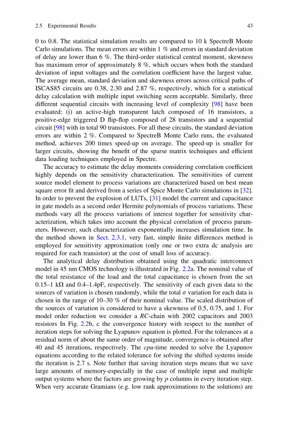
0 to 0.8. The statistical simulation results are compared to 10 k SpectreB MonteCarlo simulations. The mean errors are within 1 % and errors in standard deviationof delay are lower than 6 %. The third-order statistical central moment, skewnesshas maximum error of approximately 8 %, which occurs when both the standarddeviation of input voltages and the correlation coefficient have the largest value.The average mean, standard deviation and skewness errors across critical paths ofISCAS85 circuits are 0.38, 2.30 and 2.87 %, respectively, which for a statisticaldelay calculation with multiple input switching seem acceptable. Similarly, threedifferent sequential circuits with increasing level of complexity [98] have beenevaluated: (i) an active-high transparent latch composed of 16 transistors, apositive-edge triggered D flip-flop composed of 28 transistors and a sequentialcircuit [98] with in total 90 transistors. For all these circuits, the standard deviationerrors are within 2 %. Compared to SpectreB Monte Carlo runs, the evaluatedmethod, achieves 200 times speed-up on average. The speed-up is smaller forlarger circuits, showing the benefit of the sparse matrix techniques and efficientdata loading techniques employed in Spectre.
The accuracy to estimate the delay moments considering correlation coefficienthighly depends on the sensitivity characterization. The sensitivities of currentsource model element to process variations are characterized based on best meansquare error fit and derived from a series of Spice Monte Carlo simulations in [32].In order to prevent the explosion of LUTs, [31] model the current and capacitancein gate models as a second order Hermite polynomials of process variations. Thesemethods vary all the process variations of interest together for sensitivity char-acterization, which takes into account the physical correlation of process param-eters. However, such characterization exponentially increases simulation time. Inthe method shown in Sect. 2.3.1, very fast, simple finite differences method isemployed for sensitivity approximation (only one or two extra dc analysis arerequired for each transistor) at the cost of small loss of accuracy.
The analytical delay distribution obtained using the quadratic interconnectmodel in 45 nm CMOS technology is illustrated in Fig. 2.2a. The nominal value ofthe total resistance of the load and the total capacitance is chosen from the set0.15–1 kX and 0.4–1.4pF, respectively. The sensitivity of each given data to thesources of variation is chosen randomly, while the total r variation for each data ischosen in the range of 10–30 % of their nominal value. The scaled distribution ofthe sources of variation is considered to have a skewness of 0.5, 0.75, and 1. Formodel order reduction we consider a RC-chain with 2002 capacitors and 2003resistors In Fig. 2.2b, c the convergence history with respect to the number ofiteration steps for solving the Lyapunov equation is plotted. For the tolerances at aresidual norm of about the same order of magnitude, convergence is obtained after40 and 45 iterations, respectively. The cpu-time needed to solve the Lyapunovequations according to the related tolerance for solving the shifted systems insidethe iteration is 2.7 s. Note further that saving iteration steps means that we savelarge amounts of memory-especially in the case of multiple input and multipleoutput systems where the factors are growing by p columns in every iteration step.When very accurate Gramians (e.g. low rank approximations to the solutions) are
2.5 Experimental Results 43

selected, the approximation error of reduced system as illustrated in Fig. 2.3a isvery small compared to the Bode magnitude function of the original system. Thelower two curves correspond to the highly accurate reduced system; the proposedmodel order reduction technique delivers a system of lower order, and the uppertwo denote k = 20 reduced orders. The frequency response plot is obtained bycomputing the singular values of the transfer function H(jx), which is the fre-quency response (2.23) evaluated on the imaginary axis (Fig. 2.3b). The error plotis the frequency response plot of the singular values of the error system as a
0 1 2 3 4
x10-9
0
0.2
0.4
0.6
0.8
1
1.2
time (s)V
olta
ge (
V)/
p.d
.f.
0 10 20 30 40 5010
-15
10-10
10-5
100
norm
aliz
ed r
esid
ual n
orm
# iteration steps
iterations for Lyapunov equation GXCT+CXGT = -BBT
0 10 20 30 40 50 60
# iteration steps
iterations for Lyapunov equation GTYC+CTYG = -EE T
10-15
10-10
10-5
100
norm
aliz
ed r
esid
ual n
orm
(a)
(b)
(c)
Fig. 2.2 a Analytical delaydistribution in 45 nm CMOStechnology. Solid lineillustrates delay variance.b Convergence history ofresidual forms. Theconvergence is obtained after40 iterations. c Convergencehistory of residual forms. Theconvergence is obtained after45 iterations (� IEEE 2011)
44 2 Random Process Variation in Deep-Submicron CMOS
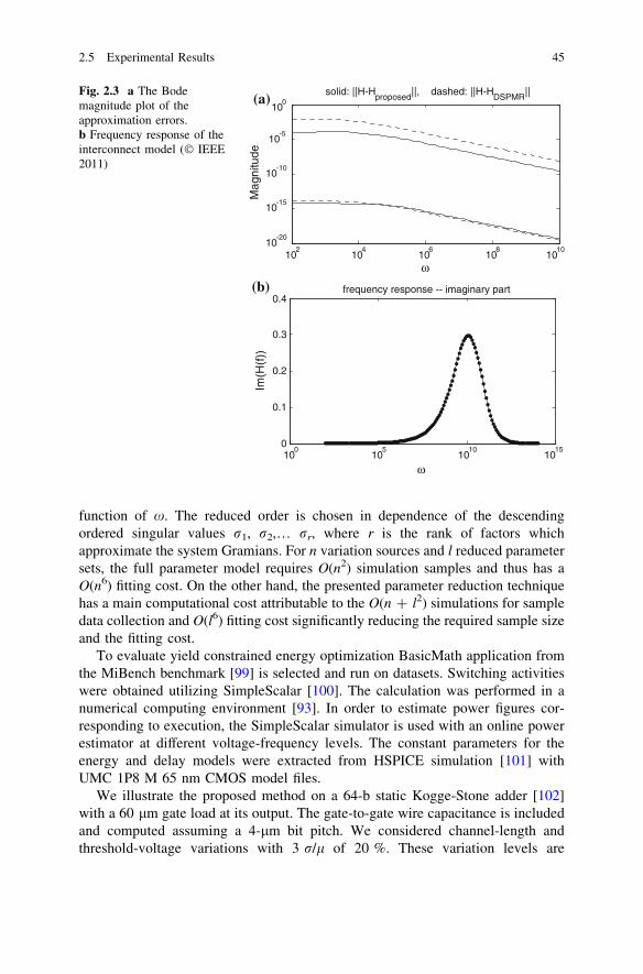
function of x. The reduced order is chosen in dependence of the descendingordered singular values r1, r2,… rr, where r is the rank of factors whichapproximate the system Gramians. For n variation sources and l reduced parametersets, the full parameter model requires O(n2) simulation samples and thus has aO(n6) fitting cost. On the other hand, the presented parameter reduction techniquehas a main computational cost attributable to the O(n ? l2) simulations for sampledata collection and O(l6) fitting cost significantly reducing the required sample sizeand the fitting cost.
To evaluate yield constrained energy optimization BasicMath application fromthe MiBench benchmark [99] is selected and run on datasets. Switching activitieswere obtained utilizing SimpleScalar [100]. The calculation was performed in anumerical computing environment [93]. In order to estimate power figures cor-responding to execution, the SimpleScalar simulator is used with an online powerestimator at different voltage-frequency levels. The constant parameters for theenergy and delay models were extracted from HSPICE simulation [101] withUMC 1P8 M 65 nm CMOS model files.
We illustrate the proposed method on a 64-b static Kogge-Stone adder [102]with a 60 lm gate load at its output. The gate-to-gate wire capacitance is includedand computed assuming a 4-lm bit pitch. We considered channel-length andthreshold-voltage variations with 3 r/l of 20 %. These variation levels are
102
104
106
108
1010
10-20
10-15
10-10
10-5
100
ωM
agni
tude
solid: ||H-Hproposed||, dashed: ||H-HDSPMR||
100
105
1010
1015
0
0.1
0.2
0.3
0.4
ω
Im(H
(f))
frequency response -- imaginary part
(a)
(b)
Fig. 2.3 a The Bodemagnitude plot of theapproximation errors.b Frequency response of theinterconnect model (� IEEE2011)
2.5 Experimental Results 45
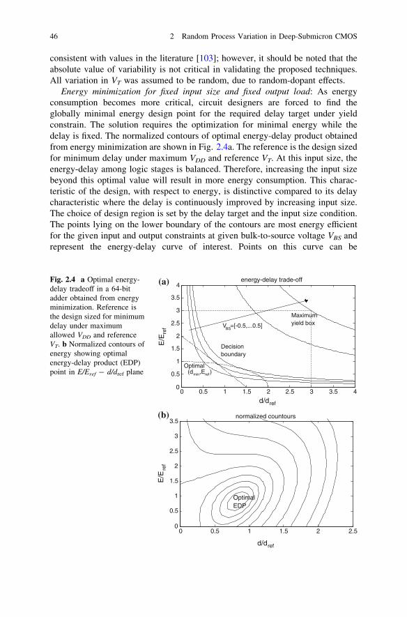
consistent with values in the literature [103]; however, it should be noted that theabsolute value of variability is not critical in validating the proposed techniques.All variation in VT was assumed to be random, due to random-dopant effects.
Energy minimization for fixed input size and fixed output load: As energyconsumption becomes more critical, circuit designers are forced to find theglobally minimal energy design point for the required delay target under yieldconstrain. The solution requires the optimization for minimal energy while thedelay is fixed. The normalized contours of optimal energy-delay product obtainedfrom energy minimization are shown in Fig. 2.4a. The reference is the design sizedfor minimum delay under maximum VDD and reference VT. At this input size, theenergy-delay among logic stages is balanced. Therefore, increasing the input sizebeyond this optimal value will result in more energy consumption. This charac-teristic of the design, with respect to energy, is distinctive compared to its delaycharacteristic where the delay is continuously improved by increasing input size.The choice of design region is set by the delay target and the input size condition.The points lying on the lower boundary of the contours are most energy efficientfor the given input and output constraints at given bulk-to-source voltage VBS andrepresent the energy-delay curve of interest. Points on this curve can be
E/E
ref
energy-delay trade-off
0 0.5 1 1.5 2 2.5 3 3.5 40
0.5
1
1.5
2
2.5
3
3.5
4
VBS
=[-0.5,...0.5]
Maximumyield box
Decisionboundary
Optimal(dmin,Eref )
d/dref
E/E
ref
normalized countours
0 0.5 1 1.5 2 2.50
0.5
1
1.5
2
2.5
3
3.5
OptimalEDP
d/dref
(a)
(b)
Fig. 2.4 a Optimal energy-delay tradeoff in a 64-bitadder obtained from energyminimization. Reference isthe design sized for minimumdelay under maximumallowed VDD and referenceVT. b Normalized contours ofenergy showing optimalenergy-delay product (EDP)point in E/Eref - d/dref plane
46 2 Random Process Variation in Deep-Submicron CMOS

determined by sizing the circuit for minimal energy under the given input size andoutput load constraint for the desired delay target. This curve is often used forenergy-delay tradeoff, where a design point is selected based on its cost of energyfor a given change in delay. The reference design moves down on the y-axis to theoptimal design point on the energy-efficient curve. With optimization, satisfyingyield constrain, we can achieve energy savings of up to 55 % without any delaypenalty. Alternatively, we can maintain the energy and achieve the speedup ofabout 25 %. Typically, only a subset of tuning variables d (e.g. gate size W, supplyvoltage VDD, bulk-to-source voltage VBS, etc.) is selected for optimization.
With a proper choice of the two variables, the designer can obtain nearly theminimal energy for a given delay. In our case, for delays close to dref, thesevariables are sizing and threshold voltage since there is the largest gap between thesizing and threshold voltage around the nominal delay point. The data in Fig. 2.4ashows that circuit optimization is really effective only in the region of about 30 %around the reference delay, dref. Outside this region, optimization becomes costlyeither in terms of delay or energy. Figure 2.4a also shows the decision boundary ofthe leakage energy corresponding to the minimal achievable energy-delay curve.The leakage curve is primarily affected by the large circuit size variation withrespect to delay change. The increased leakage associated with a longer clockcycle is substantially less than the leakage reduction obtained from smaller tran-sistor sizes. Therefore, leakage energy behaves as similarly as the active energy.Even when leakage energy becomes comparable to the active energy in futuretechnologies or due to low switching activity of circuits, the characteristics of theminimal achievable energy-delay curve will remain unchanged and no algorithmicchange for the optimization is needed. The obtained statistics of the total energyconsumption for the benchmark circuit is compared with Monte Carlo basedsimulations. The results show that the estimates obtained using the proposedapproach for the values of the mean delay and leakage energy are very accuratewith an average error of 1.2 and 1.8 %, respectively. The standard deviations showan average error of 3.6 and 7.7 % for energy and delay, respectively.
Energy optimization for fixed input size and fixed output load: Energy opti-mization for a fixed input size and output load constraint is the most commondesign scenario. The plot in Fig. 2.4b illustrates the position of the optimal energy-delay product for 64-b static Kogge-Stone adder under maximum yield referencedesign point for the adder relative to the optimal energy-delay tradeoff curveobtained by jointly optimizing gate size, supply and threshold voltages. Throughoptimization, the input vectors are divided into a number of sub-sets. The opti-mization problem is solved incrementally, covering all the sub-sets of classesconstructing the optimal separating hyperplane for the full data set. Note thatduring this process the value of the functional vector of parameters is monotoni-cally increasing, since more and more training vectors are considered in theoptimization leading to efficient separation between the two classes. In symmet-rical circuit structures, the optimization space is limited and therefore the addi-tional energy saving contributed by optimization is much smaller, especially withthe higher timing yield. For decreased timing yield, higher energy saving can be
2.5 Experimental Results 47
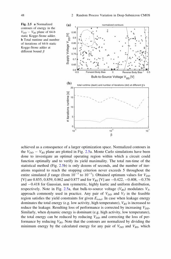
achieved as a consequence of a larger optimization space. Normalized contours inthe VDD - VBS plane are plotted in Fig. 2.5a. Monte Carlo simulations have beendone to investigate an optimal operating region within which a circuit couldfunction optimally and to verify its yield maximality. The total run-time of thestatistical method (Fig. 2.5b) is only dozens of seconds, and the number of iter-ations required to reach the stopping criterion never exceeds 5 throughout theentire simulated b range (from 10-3 to 10-1). Obtained optimum values for VDD
[V] are 0.855, 0.859, 0.862 and 0.877 and for VBS [V] are -0.422, -0.408, -0.376and -0.418 for Gaussian, non symmetric, highly kurtic and uniform distribution,respectively. Note in Fig. 2.5a, that bulk-to-source voltage (VBS) modulates VT,approach commonly used in practice. Any pair of VDD and VT in the feasibleregion satisfies the yield constraints for given Etotal. In case when leakage energydominates the total energy (e.g. low activity, high temperature), VBS is increased toreduce the leakage. Resulting loss of performance is corrected by increasing VDD.Similarly, when dynamic energy is dominant (e.g. high activity, low temperature),the total energy can be reduced by reducing VDD and correcting the loss of per-formance by reducing VBS. Note that the contours are normalized by dividing theminimum energy by the calculated energy for any pair of VDD and VBS, which
-0.5 0 0.50.6
0.65
0.7
0.75
0.8
0.85
0.9
0.95
1
Bulk-to-Source Voltage VBS [V]
Sup
ply
Vol
tage
VD
D [V]
normalized contours
Forward Body Bias Reverse Body Bias
10-3
10-2
10-1
0
5
10
15
20
β
total runtime (dash) and number of iterations (dot) at different β's
# ita
ratio
ns r
untim
e [s
]
(a)
(b)
Fig. 2.5 a Normalizedcontours of energy in theVDD - VBS plane of 64-bstatic Kogge-Stone adder.b Total runtime and numberof iterations of 64-b staticKogge-Stone adder atdifferent bound b
48 2 Random Process Variation in Deep-Submicron CMOS
satisfy the yield constraints. To set tight constraints, the maximum allowedfrequency can be lowered or the acceptable ratio of leakage to total power can bereduced. However, in an application for which activity of the circuit is high, theincrease in the size of the transistors reduces the yield as a consequence of theincreased transistors’ parasitic capacitance. As yield increases when tolerancedecreases, agreeable tradeoff needs to exist between increase in yield and the costof design and manufacturing. Consequently, continuous observation of processvariation and thermal monitoring becomes a necessity [104].
2.6 Conclusions
Statistical simulation is one of the foremost steps in the evaluation of successfulhigh-performance IC designs due to process variations, which strongly affectdevices behavior in today’s deep submicron technologies. In this chapter, ratherthan estimating statistical behavior of the circuit by a population of realizations,we describe integrated circuits as a set of stochastic differential equations andintroduce Gaussian closure approximations to obtain a closed form of momentequations. The static manufacturing variability and dynamic statistical fluctuationare treated separately. Process variations are modeled as a wide-sense stationaryprocess and the solution of MNA for such a process is found. Similarly, we presenta novel method to extend voltage-based gate models for statistical timing analysis.We constructed gate models based on statistical simplified transistor models forhigher accuracy. Correlations among input signals and between input signal anddelay are preserved during simulation by using same model format for the voltageand all elements in gate models. Furthermore, the multiple input simultaneousswitching problem is addressed by considering all input signals together for outputinformation. Since the proposed timing analysis is based on the transistor-levelgate models, it is able to handle both combinational and sequential circuits. Theexperiments demonstrated the good combination of accuracy and efficiency of theproposed method for both deterministic and statistical timing analysis. Addition-ally, we present an efficient methodology for interconnect model reduction basedon adjusted dominant subspaces projection. By adopting the parameter dimensionreduction techniques, interconnect model extraction can be performed in thereduced parameter space, thus provide significant reductions on the requiredsimulation samples for constructing accurate models. Extensive experiments areconducted on a large set of random test cases, showing very accurate results.Furthermore, we presented energy and yield constrained optimization as an activedesign strategy. We create a sequence of minimizations of the feasible region withiteratively-generated low-dimensional subspaces. As the resulting sub-problemsare small, global optimization in both convex and non-convex cases is possible.The method can be used with any variability model, and is not restricted to anyparticular performance constraint. The effectiveness of the proposed approach isevaluated on a 64-b static Kogge-Stone adder implemented in UMC 1P8 M 65 nm
2.5 Experimental Results 49
technology. As the experimental results indicate, the suggested numerical methodsprovide accurate and efficient solutions of energy optimization problem offering ofup to 55 % energy savings.
References
1. K. Bowman, J. Meindl, Impact of within-die parameter fluctuations on the future maximumclock frequency distribution. Proceedings of IEEE Custom Integrated Circuits Conference,pp. 229–232 (2001)
2. T. Mizuno, J. Okamura, A. Toriumi, Experimental study of threshold voltage fluctuationdue to statistical variation of channel dopant number in MOSFET’s. IEEE Trans. ElectronDevices 41, 2216–2221 (1994)
3. A. Asenov, S. Kaya, J.H. Davies, Intrinsic threshold voltage fluctuations in MOSFETs dueto local oxide thickness variations. IEEE Trans. Electron Devices 49(1), 112–119 (2002)
4. J.A. Croon, G. Storms, S. Winkelmeier, I. Pollentier, Line-edge roughness: characterization,modeling, and impact on device behavior. Proceedings of IEEE International ElectronicDevices Meeting, pp. 307–310 (2002)
5. A. Asenov, G. Slavcheva, A.R. Brown, J. Davies, S. Saini, Increase in the random dopantinduced threshold fluctuations and lowering in sub-100 nm MOSFETs due to quantumeffects: a 3-D density-gradient simulation study. IEEE Trans. Electron Devices 48(4),722–729 (2001)
6. J. Kwong, A. Chandrakasan, Variation driven device sizing for minimum energysubthreshold circuits. IEEE International Symposium on Low-Power Electronic Design,pp. 8–13 (2006)
7. M. Horowitz, E. Alon, D. Patil, S. Naffziger, R. Kumar, K. Bernstein, Scaling, power, andthe future of CMOS. IEEE International Electronic Devices Meeting, pp. 7–15 (2005)
8. D. Markovic et al., Ultralow-power design in near-threshold region. Proc. IEEE 98(2),237–252 (2010)
9. K. Itoh, Adaptive circuits for the 0.5-V nanoscale CMOS era. Digest of Techical PapersIEEE International Solid-State Circuits Conference, pp. 14–20. (2009)
10. M. Grigoriu, On the spectral representation method in simulation. Probab. Eng. Mech. 8,75–90 (1993)
11. M. Loève, Probability Theory (D. Van Nostrand Company Inc., Princeton, 1960)12. R. Ghanem, P.D. Spanos, Stochastic Finite Element: A Spectral Approach (Springer, New
York, 1991)13. P. Friedberg, Y. Cao, J. Cain, R. Wang, J. Rabaey, C. Spanos, Modeling within-die spatial
correlation effects for process-design co-optimization. IEEE International Symposium onQuality of Electronic Design, pp. 516–521 (2005)
14. J. Xiong, V. Zolotov, L. He, Robust extraction of spatial correlation. Proceedings of IEEEInternational Symposium on Physical Design, pp. 2–9 (2006)
15. M. Pelgrom, A. Duinmaijer, A. Welbers, Matching properties of MOS transistors. IEEE J.Solid-State Circuits 24(5), 1433–1439 (1989)
16. C. Michael, M. Ismail, Statistical Modeling for Computer-Aided Design of MOS VLSICircuits (Kluwer, Boston, 1993)
17. H. Zhang, Y. Zhao, A. Doboli, ALAMO: an improved r-space based methodology formodeling process parameter variations in analog circuits. Proceedings of IEEE Design,Automation and Test in Europe Conference, pp. 156–161 (2006)
18. R. López-Ahumada, R. Rodríguez-Macías, FASTEST: a tool for a complete and efficientstatistical evaluation of analog circuits, dc analysis. Analog Integr. Circ. Sig. Process. 29(3),201–212 (2001)(Kluwer Academic Publishers)
50 2 Random Process Variation in Deep-Submicron CMOS

19. G. Biagetti, S. Orcioni, C. Turchetti, P. Crippa, M. Alessandrini, SiSMA-a statisticalsimulator for mismatch analysis of MOS ICs. Proceedings of IEEE/ACM InternationalConference on Computer Aided Design, pp. 490–496 (2002)
20. B. De Smedt, G. Gielen, WATSON: design space boundary exploration and modelgeneration for analogue and RF IC design. IEEE Trans. CAD Integr. Circuits Syst. 22(2),213–224 (2003)
21. B. Linares-Barranco, T. Serrano-Gotarredona, On an efficient CAD implementation of thedistance term in Pelgrom’s mismatch model. IEEE Trans. CAD Integr. Circuits Syst. 26(8),1534–1538 (2007)
22. J. Kim, J. Ren, M.A. Horowitz, Stochastic steady-state and ac analyses of mixed-signalsystems. Proceedings of IEEE Design Automation Conference, pp. 376–381 (2009)
23. A. Zjajo, J. Pineda de Gyvez, Analog automatic test pattern generation for quasi-staticstructural test. IEEE Trans. VLSI Syst. 17(10), 1383–1391 (2009)
24. N. Mi, J. Fan, S.X.-D. Tan, Y. Cai, X. Hong, Statistical analysis of on-chip power deliverynetworks considering lognormal leakage current variations with spatial correlation. IEEETrans. Circuits Syst. I Regul. Pap. 55(7), 2064–2075 (2008)
25. E. Felt, S. Zanella, C. Guardiani, A. Sangiovanni-Vincentelli, Hierarchical statisticalcharacterization of mixed-signal circuits using behavioral modeling. Proceedings of IEEEInernational Conference on Computer Aided Design, pp. 374–380 (1996)
26. J. Vlach, K. Singhal, Computer Methods for Circuit Analysis and Design (Van NostrandReinhold, New York, 1983)
27. L.O. Chua, C.A. Desoer, E.S. Kuh, Linear and Nonlinear Circuits (Mc Graw-Hill, NewYork, 1987)
28. L. Arnold, Stochastic Differential Equations: Theory and Application (Wiley, New York,1974)
29. S. Bhardwaj, S. Vrudhula, A. Goel, A unified approach for full chip statistical timing andleakage analysis of nanoscale circuits considering intradie process variations. IEEE Trans.Comput. Aided Des. Integr. Circuits Syst. 27(10), 1812–1825 (2008)
30. J.F. Croix, D.F. Wong, A fast and accurate technique to optimize characterization tables forlogic sythesis. Proceedings of IEEE Design Automation Conference, pp. 337–340 (1997)
31. A. Goel, S. Vrudhula, Statistical waveform and current source based standard cell modelsfor accurate timing analysis. Proceedings of IEEE Design Automation Conference,pp. 227–230 (2008)
32. H. Fatemi, S. Nazarian, M. Pedram, Statistical logic cell delay analysis using a current-based model. Proceedings of IEEE Design Automation Conference, pp. 253–256 (2006)
33. B. Liu, A.B. Kahng, Statistical gate level simulation via voltage controlled current sourcemodels. Proceedings of IEEE International Workshop on Behavioral Modeling andSimulation, p. 23–27 (2006)
34. B. Liu, Gate level statistical simulation based on parameterized models for process andsignal variations. Proceedings of IEEE International Symposium on Quality ElectronicDesign, pp. 257–262 (2007)
35. J.F. Croix, D.F. Wong, Blade and Razor: cell and interconnet delay analysis using current-based models. Proceedings of IEEE Design Automation Conference, pp. 386–389 (2003)
36. C. Amin, C. Kashyap, N. Menezes, K. Killpack, E. Chiprout, A multi-port current sourcemodel for multiple-input switching effects in CMOS library cells. Proceedings of IEEEDesign Automation Conference, pp. 247–252 (2006)
37. C. Kashyap, C. Amin, N. Menezes, E. Chiprout, A nonlinear cell macromodel for digitalapplications. Proceedings of IEEE International Conference on Computer Aided Design,pp. 678–685 (2007)
38. N. Menezes, C. Kashyap, C. Amin, A true electrical cell model for timing, noise, and powergrid verification. Proceedings of IEEE Design Automation Conference, pp. 462–467 (2008)
39. B. Amelifard, S. Hatami, H. Fatemi, M. Pedram, A current source model for CMOS logiccells considering multiple input switching and stack effect. Proceedings of IEEE Design,Automation and Test in Europe Conference, pp. 568–574 (2008)
References 51
40. A. Devgan, Accurate device modeling techniques for efficient timing simulation ofintegrated circuits. Proceedings of IEEE International Conference on Computer Design,pp. 138–143 (1995)
41. F. Dartu, Gate and transistor level waveform calculation for timing analysis. Ph.D.Dissertation, Carnegie Mellon University, 1997
42. P. Kulshreshtha, R. Palermo, M. Mortazavi, C. Bamji, H. Yalcin, Transistor-level timinganalysis using embedded simulation. Proceedings of IEEE International Conference onComputer Aided Design, pp. 344–349 (2000)
43. P.F. Tehrani, S.W. Chyou, U. Ekambaram, Deep sub-micron static timing analysis inpresence of crosstalk. Proceedings of IEEE International Symposium on Quality ElectronicDesign, pp. 505–512 (2000)
44. E. Acar, Linear-centric simulation approach for timing analysis. Ph.D. dissertation,Carnegie Mellon University, 2001
45. E. Acar, F. Dartu, L. Pileggi, TETA: transistor-level waveform evaluation for timinganalysis. IEEE Trans. Comput. Aided Des. Integr. Circuits Syst. 21(5), 605–616 (2002)
46. L. McMurchie, C. Sechen, WTA-waveform-based timing analysis for deep-micro circuits.Proceedings of IEEE International Conference on Computer Aided Design, pp. 625–631(2002)
47. Z. Wang, J. Zhu, Transistor-level static timing analysis by piecewise quadratic waveformmatching. Proceedings of IEEE Design, Automation and Test in Europe Conference,pp. 312–317 (2003)
48. S. Raja, Varadi, M. Becer, J. Geada, Transistor level gate modeling for accurate and fasttiming, noise, and power analysis. Proceedings of IEEE Design Automation Conference,pp. 456–461 (2008)
49. Q. Tang, A. Zjajo, M. Berkelaar, N. van der Meijs, Transistor level waveform evaluation fortiming analysis. in Proceedings of European Workshop on CMOS Variability, pp. 1–6(2010)
50. J.F. Epperson, An Introduction to Numerical Methods and Analysis (John Wiley & Sons,Inc, New York, 2002)
51. T. Shima, H. Yamada, R.L.M. Dang, Table look-up mosfet modeling system using a 2-ddevice simulator and monotonic piecewise cubic interpolation. IEEE Trans. Comput. AidedDes. 2(2), 121–126 (1983)
52. P.E. Allen, K.S. Yoon, A table look-up model for analog applications. InternationalConference on Computer-Aided Design, pp. 124–127 (1988)
53. Pathmill: Transistor-level static timing analysis, [online], available at: http://www.synopysys.com/products/analysis/pathmillds.pdf
54. Q. Tang, A. Zjajo, M. Berkelaar, N. van der Meijs, A simplified transistor model for cmostiming analysis. Proceedings of Workshop on circuits, systems and signal processing,pp. 289–294 (2009)
55. M. Chen, W. Zhao, F. Liu, Y. Cao, Fast statistical circuit analysis with finite-point basedtransistor model. Proceedings of IEEE Design, Automation and Test in Europe Conference,pp. 1–6 (2007)
56. A. Hyvarinen, E. Oja, Independent component analysis: algorithms and applications. NeuralNetworks J. 13(4/5), 411–430 (2000)
57. R. Manduchi, J. Portilla, Independent component analysis of textures. Proc. IEEE Int. Conf.Comput. Vis. 2, 1054–1060 (1999)
58. Z. Feng, P. Li, Y. Zhan, Fast second-order statistical static timing analysis using parameterdimension reduction. Proceedings of IEEE Design Automation Conference, pp. 244–249(2007)
59. C. Visweswariah et al., First-order incremental block-based statistical timing analysis. IEEETrans. Comput. Aided Des. Integr. Circuits Syst. 25(10), 2170–2180 (2006)
60. T.T. Soong, Random Diffrential Equations in Science and Engineering (Academic Press,New York, 1973)
52 2 Random Process Variation in Deep-Submicron CMOS
61. Q. Tang, A. Zjajo, M. Berkelaar, N. P. van der Meijs, RDE-based transistor-level gatesimulation for statistical static timing analysis. Proceedings of IEEE Design AutomationConference, pp. 787–792 (2010)
62. Q. Tang, A. Zjajo, M. Berkelaar, N.P. van der Meijs, Statistical delay calculation withmultiple input simultaneous switching. Proceedings of IEEE International Conference onIC Design and Technology, pp. 1–4 (2011)
63. L.T. Pillage, R.A. Rohrer, Asymptotic waveform evaluation for timing analysis. IEEETrans. Comput. Aided Des. Integr. Circuits Syst. 4, 352–366 (1990)
64. P. Feldmann, R.W. Freund, Efficient linear circuit analysis by Pade approximation via theLanczos process. IEEE Trans. Comput. Aided Des. Integr. Circuits Syst. 14, 639–649(1995)
65. A. Odabasioglu, M. Celik, L. Pileggi, PRIMA: Passive reduced-order interconnectmacromodeling algorithm. IEEE Transactions on Computer-Aided Design of IntegratedCircuits and Systems, pp. 645–654 (1998)
66. P. Elias, N. van der Meijs, Including higher-order moments of RC interconnections inlayout-to-circuit extraction. Proceedings of IEEE Design, Automation and Test in EuropeConference, pp. 362–366 (1996)
67. B.C. Moore, Principal component analysis in linear systems: controllability, observability,and model reduction. IEEE Trans. Autom. Control 26, 17–31 (1981)
68. J. Li, J. White, Efficient model reduction of interconnect via approximate systemGrammians. Proceedings of IEEE International Conference on Computer Aided Design,pp. 380–384 (1999)
69. J.R. Phillips, L. Daniel, L.M. Silveira, Guaranteed passive balancing transformations formodel order reduction. Proceedings of IEEE Design Automation Conference, pp. 52–57(2002)
70. J.R. Phillips, L.M. Silveira, Poor man’s TBR: a simple model reduction scheme.Proceedings of IEEE Design, Automation and Test in Europe Conference, pp. 938–943(2004)
71. W.F. Arnold, A.J. Laub, Generalized eigenproblem algorithms and software for algebraicRiccati equation. Proc. IEEE 72, 1746–1754 (1984)
72. T. Penzl, A cyclic low-rank Smith method for large sparse Lyapunov equations. SIAM J.Sci. Comput. 21, 1401–1418 (2000)
73. M.G. Safonov, R.Y. Chiang, A Schur method for balanced-truncation model reduction.IEEE Trans. Autom. Control 34, 729–733 (1989)
74. K.V. Fernando, H. Nicholson, Singular perturbational model reduction of balanced systems.IEEE Trans. Autom. Control 27, 466–468 (1982)
75. D. Enns, Model reduction with balanced realizations: an error bound and a frequencyweighted generalization. Proceedings of IEEE Conference on Decision and Control,pp. 127–132 (1984)
76. M.S. Tombs, I. Postlethwaite, Truncated balanced realization of stable, non-minimal state-space systems. Int. J. Control 46, 1319–1330 (1987)
77. G. Golub, C. van Loan, Matrix Computations (Johns Hopkins University Press, BaltimoreMD, 1996)
78. J. Singh, V. Nookala, Z. Luo, S. Sapatnekar, Robust gate sizing by geometric programming.Proceedings of IEEE Design Automation Conference, pp. 315–320 (2005)
79. D. Nguyen et al., Minimization of dynamic and static power through joint assignment ofthreshold voltages and sizing optimization. Proceedings of IEEE International Symposiumon Low Power Electronic Design, pp. 158–163 (2003)
80. R. Brodersen et al., Methods for true power minimization. Proceedings of IEEEInternational Conference on Computer-Aided Design, pp. 35–42 (2002)
81. K. Nose, T. Sakurai, Optimization of VDD and VTH for low power and high-speedapplications. Proceedings of IEEE Design Automation Conference, pp. 469–474 (2000)
82. A. Bhavnagarwala, B. Austin, K. Bowman, J.D. Meindl, A minimum total power methodologyfor projecting limits on CMOS GSI. IEEE Trans. VLSI Syst. 8(6), 235–251 (2000)
References 53
83. M. Mani, A. Devgan, M. Orshansky, An efficient algorithm for statistical minimization oftotal power under timing yield constraints. Proceedings of IEEE Design AutomationConference, pp. 309–314 (2005)
84. A. Srivastava, K. Chopra, S. Shah, D. Sylvester, D. Blaauw, A novel approach to performgate-level yield analysis and optimization considering correlated variations in power andperformance. IEEE Trans. Comput. Aided Des. 27(2), 272–285 (2008)
85. C. Gu, J. Roychowdhury, An efficient, fully nonlinear, variability-aware non-Monte-Carloyield estimation procedure with applications to SRAM cells and ring oscillators. Proceedingsof IEEE Asia-South Pacific Design Automation Conference, pp. 754–761 (2008)
86. M. Meijer, J. Pineda de Gyvez, Body bias driven design synthesis for optimum performanceper area. Proceedings of IEEE International Symposium on Quality Electronic Design,pp. 472–477 (2010)
87. A. Zjajo, Q. Tang, M. Berkelaar, J. Pineda de Gyvez, A. Di Bucchianico, N. van der Meijs,Stochastic analysis of deep-submicrometer CMOS process for reliable circuits designs.IEEE Trans. Circuits Syst. I Regul. Pap. 58(1), 164–175 (2011)
88. Y. Freund, R.E. Schapire, Large margin classification using the perceptron algorithm. Mach.Learn. 37, 277–296 (1999)
89. I. Tsochantaridis, T. Hofmann, T. Joachims, Y. Altun, Support vector machine learning forinterdependent and structured output spaces. Proceedings of of International Conference onMachine Learning, pp. 1–8 (2004)
90. J.C. Platt, Fast training of support vector machines using sequential minimal optimization,in Advances in Kernel Methods: Support Vector Learning, ed. by B. Scholkopf, C.J.C.Burges, A.J. Smola (MIT Press, Cambridge, 1998) pp. 195–208
91. B. Taskar, Learning structured prediction models: a large margin approach, PhD thesis,Stanford University, 2004
92. V. Franc, V. Hlavac, Multi-class support vector machine. Proc. IEEE Int. Conf. PatternRecognit. 2, 236–239 (2002)
93. MatLab, http://www.mathworks.com/94. A. Zjajo, M. Song, Digitally programmable continuous-time biquad filter in 65-nm CMOS.
Proceedings of IEEE International Symposium on Radio-Frequency IntegrationTechnology, pp. 339–342 (2009)
95. Nangate 45 nm open cell library (2009), http://www.nangate.com/ index.php?option =
comcontent&task = view&id = 137&Itemid = 13796. X. Lu, W.P. Shi., Layout and parasitic information for ISCAS circuits (2004), http://
dropzone.tamu.edu/xiang/iscas.html97. X. Zheng, Implementing and evaluating a simplified transistor model for timing analysis of
integrated circuits, Master’s thesis, Delft University of Technology, 201298. J. Rodriguez, Q. Tang, A. Zjajo, M. Berkelaar, N. van der Meijs, Direct statistical simulation
of timing properties in sequential circuits. Proceedings of International Workshop on Powerand Timing Modeling, Optimization ans Simulation, pp. 131–141 (2012)
99. MiBench, http://www.eecs.umich.edu/mibench/100. SimpleScalar, http://www.simplescalar.com/101. HSPICE Simulation and Analysis User Guide, Version W-2005.03, Synopsys, Mountain
View, CA, 2005102. P.M. Kogge, H.S. Stone, A parallel algorithm for the efficient solution of general class of
recurrence equations. IEEE Trans. Comput. C-22(8), 786–793 (1973)103. K. Bernstein et al., High-performance CMOS variability in the 65 nm regime and beyond.
IBM J. Res. Dev. 50(4/5), 433–449 (2006)104. A. Zjajo, M.J. Barragan, J. Pineda de Gyvez, Low-power die-level process variation and
temperature monitors for yield analysis and optimization in deep-submicron CMOS. IEEETrans. Instrum. Meas. 61(8), 2212–2221 (2012)
54 2 Random Process Variation in Deep-Submicron CMOS
Chapter 3Electrical Noise in Deep-SubmicronCMOS
In addition to device variability, which sets the limitations of circuit designs interms of accuracy, linearity and timing, existence of electrical noise associatedwith fundamental processes in integrated-circuit devices represents an elementarylimit on the performance of electronic circuits. The existence of electrical noise isessentially due to the fact that electrical charge is not continuous, but is carried indiscrete amounts equal to the electron charge. The noise phenomena consideredhere are caused by the small current and voltage fluctuations, such as thermal, shot,and flicker noise, that are generated within the integrated-circuit devicesthemselves.
The noise performance of a circuit can be analyzed in terms of the small-signalequivalent circuits by considering each of the uncorrelated noise sources in turnand separately computing their contribution at the output. A nonlinear circuit isassumed to have time-invariant (dc) large-signal excitations and time-invariantsteady-state large-signal waveforms and that both the noise sources and the noiseat the output are wide-sense stationary stochastic processes. Subsequently, thenonlinear circuit is linearized around the fixed operating point to obtain a lineartime-invariant network for noise analysis. Implementation of this method based onthe interreciprocal adjoint network concept [1] results in a very efficient compu-tational technique for noise analysis, which is available in almost every circuitsimulator. Unfortunately, this method is only applicable to circuits with fixedoperating points and is not appropriate for noise simulation of circuits withchanging bias conditions.
In a noise simulation method that uses linear periodically time-varying trans-formations [2, 3], a nonlinear circuit is assumed to have periodic large signalexcitations and periodic steady-state large-signal waveforms and that both thenoise sources and the noise at the output are cyclostationary stochastic processes.Afterward, the nonlinear circuit is linearized around the periodic steady-stateoperating-point to obtain a linear periodically time-varying network for noiseanalysis. Nevertheless, this noise analysis technique is applicable to only a limitedclass of nonlinear circuits with periodic excitations.
Noise simulation in time-domain has traditionally been based on the MonteCarlo technique [4], where the circuit with the noise sources is simulated using
A. Zjajo, Stochastic Process Variation in Deep-Submicron CMOS, Springer Seriesin Advanced Microelectronics 48, DOI: 10.1007/978-94-007-7781-1_3,� Springer Science+Business Media Dordrecht 2014
55

numerous transient analyzes with different sample paths of the noise sources.Consequently, the probabilistic characteristics of noise are then calculated usingthe data obtained in these simulations. However, accurately determining the noisecontent requires a large number of simulations, so consequently, Monte Carlomethod becomes very cpu-time consuming if the chip becomes large. Addition-ally, to accurately model shot and thermal noise sources, time-step in transientanalysis is limited to a very small value, making the simulation highly inefficient.
In this chapter, we treat the noise as a non-stationary stochastic process, andintroduce an Itô system of stochastic differential equations (SDE) as a convenientway to represent such a process. Recognizing that the variance-covariance matrixwhen backward Euler is applied to such a matrix can be written in the continuous-time Lyapunov matrix form, we then provide a numerical solution to such a set oflinear time-varying equations. We adapt model description as defined in [5], wherethermal and shot noise are expressed as delta-correlated noise processes havingindependent values at every time point, modeled as modulated white noise pro-cesses. These noise processes correspond to current noise sources which areincluded in the models of the integrated-circuit devices. As numerical experimentssuggest that both the convergence and stability analyses of adaptive schemes forstochastic differential equations extend to a number of sophisticated methodswhich control different error measures, we follow the adaptation strategy, whichcan be viewed heuristically as a fixed time-step algorithm applied to a timere-scaled differential equation. Additionally, adaptation also confers stability onalgorithms constructed from explicit time-integrators, resulting in better qualita-tive behavior than for fixed time-step counter-parts [6].
The chapter is organized as follows: Section 3.1 focuses on the electrical noisemodeled as a non-stationary process and discusses a solution of a system ofstochastic differential equations for such process. In Sect. 3.2, error sources whichcan cause loss of simulation accuracy are evaluated. In Sect. 3.3, the adaptivenumerical methods control the time-step error is discussed. Section 3.4 focuses onthe discrete recursive algorithm for noise content contribution estimation.Experimental results obtained are presented in Sect. 3.5. Finally, Sect. 3.6 pro-vides a summary and the main conclusions.
3.1 Stochastic MNA for Noise Analysis
The most important types of electrical noise sources (thermal, shot, and flickernoise) in passive elements and integrated circuit devices have been investigatedextensively, and appropriate models have been derived [7] as stationary and in [5]as non-stationary noise sources. We adapt model descriptions as defined in [5],where thermal and shot noise are expressed as delta-correlated noise processeshaving independent values at every time point, modeled as modulated white noiseprocesses. These noise processes correspond to the current noise sources which areincluded in the models of the integrated-circuit devices.
56 3 Electrical Noise in Deep-Submicron CMOS
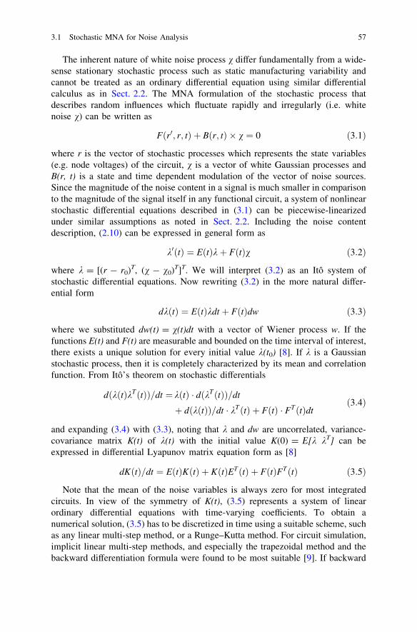
The inherent nature of white noise process v differ fundamentally from a wide-sense stationary stochastic process such as static manufacturing variability andcannot be treated as an ordinary differential equation using similar differentialcalculus as in Sect. 2.2. The MNA formulation of the stochastic process thatdescribes random influences which fluctuate rapidly and irregularly (i.e. whitenoise v) can be written as
Fðr0; r; tÞ þ Bðr; tÞ � v ¼ 0 ð3:1Þ
where r is the vector of stochastic processes which represents the state variables(e.g. node voltages) of the circuit, v is a vector of white Gaussian processes andB(r, t) is a state and time dependent modulation of the vector of noise sources.Since the magnitude of the noise content in a signal is much smaller in comparisonto the magnitude of the signal itself in any functional circuit, a system of nonlinearstochastic differential equations described in (3.1) can be piecewise-linearizedunder similar assumptions as noted in Sect. 2.2. Including the noise contentdescription, (2.10) can be expressed in general form as
k0ðtÞ ¼ EðtÞkþ FðtÞv ð3:2Þ
where k = [(r - r0)T, (v - v0)T]T. We will interpret (3.2) as an Itô system ofstochastic differential equations. Now rewriting (3.2) in the more natural differ-ential form
dkðtÞ ¼ EðtÞkdt þ FðtÞdw ð3:3Þ
where we substituted dw(t) = v(t)dt with a vector of Wiener process w. If thefunctions E(t) and F(t) are measurable and bounded on the time interval of interest,there exists a unique solution for every initial value k(t0) [8]. If k is a Gaussianstochastic process, then it is completely characterized by its mean and correlationfunction. From Itô’s theorem on stochastic differentials
dðkðtÞkTðtÞÞ=dt ¼ kðtÞ � dðkTðtÞÞ=dt
þ dðkðtÞÞ=dt � kTðtÞ þ FðtÞ � FTðtÞdtð3:4Þ
and expanding (3.4) with (3.3), noting that k and dw are uncorrelated, variance-covariance matrix K(t) of k(t) with the initial value K(0) = E[k kT] can beexpressed in differential Lyapunov matrix equation form as [8]
dKðtÞ=dt ¼ EðtÞKðtÞ þ KðtÞETðtÞ þ FðtÞFTðtÞ ð3:5Þ
Note that the mean of the noise variables is always zero for most integratedcircuits. In view of the symmetry of K(t), (3.5) represents a system of linearordinary differential equations with time-varying coefficients. To obtain anumerical solution, (3.5) has to be discretized in time using a suitable scheme, suchas any linear multi-step method, or a Runge–Kutta method. For circuit simulation,implicit linear multi-step methods, and especially the trapezoidal method and thebackward differentiation formula were found to be most suitable [9]. If backward
3.1 Stochastic MNA for Noise Analysis 57
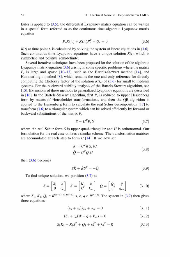
Euler is applied to (3.5), the differential Lyapunov matrix equation can be writtenin a special form referred to as the continuous-time algebraic Lyapunov matrixequation
PrKðtrÞ þ KðtrÞPTr þ Qr ¼ 0 ð3:6Þ
K(t) at time point tr is calculated by solving the system of linear equations in (3.6).Such continuous time Lyapunov equations have a unique solution K(t), which issymmetric and positive semidefinite.
Several iterative techniques have been proposed for the solution of the algebraicLyapunov matrix equation (3.6) arising in some specific problems where the matrixPr is large and sparse [10–13], such as the Bartels-Stewart method [14], andHammarling’s method [8], which remains the one and only reference for directlycomputing the Cholesky factor of the solution K(tr) of (3.6) for small to mediumsystems. For the backward stability analysis of the Bartels-Stewart algorithm, see[15]. Extensions of these methods to generalized Lyapunov equations are describedin [16]. In the Bartels-Stewart algorithm, first Pr is reduced to upper Hessenbergform by means of Householder transformations, and then the QR-algorithm isapplied to the Hessenberg form to calculate the real Schur decomposition [17] totransform (3.6) to a triangular system which can be solved efficiently by forward orbackward substitutions of the matrix Pr
S ¼ UT PrU ð3:7Þ
where the real Schur form S is upper quasi-triangular and U is orthonormal. Ourformulation for the real case utilizes a similar scheme. The transformation matricesare accumulated at each step to form U [14]. If we now set
~K ¼ UT KðtrÞU~Q ¼ UT QrU
ð3:8Þ
then (3.6) becomes
S~K þ ~KST ¼ �~Q ð3:9Þ
To find unique solution, we partition (3.7) as
S ¼ S1 s0 tn
ffi �~K ¼ K1 k
kT knn
ffi �~Q ¼ Q1 q
qT qnn
ffi �ð3:10Þ
where S1, K1, Q1 [ R(n-1) 9 (n-1); s, k, q [ R(n-1). The system in (3.7) then givesthree equations
ðtn þ �tnÞknn þ qnn ¼ 0 ð3:11Þ
ðS1 þ �tnIÞk þ qþ knns ¼ 0 ð3:12Þ
S1K1 þ K1ST1 þ Q1 þ skT þ ksT ¼ 0 ð3:13Þ
58 3 Electrical Noise in Deep-Submicron CMOS
knn can be obtained from (3.10) and set in (3.11) to solve for k. Once k is known,(3.12) becomes a Lyapunov equation which has the same structure as (3.9) but oforder (n-1), as
S1K1 þ K1ST1 ¼ �Q1 � skT � ksT ð3:14Þ
We can apply the same process to (3.13) until S1 is of the order -1. Note underthe condition that i = 1,…, n at the kth step (k = 1, 2,…, n) of this process, we canobtain a unique solution vector of length (n ? 1-k) and a reduced triangularmatrix equation of order (n-k). Since U is orthonormal, once (3.9) is solved for ~K,then K(tr) can be computed using
KðtrÞ ¼ U ~KUT ð3:15Þ
Large dense Lyapunov equations can be solved by sign function based tech-niques [17]. Krylov subspace methods, which are related to matrix polynomialshave been proposed [18] as well.
Relatively large sparse Lyapunov equations can be solved by iterativeapproaches, [19]. Here, we apply a low rank version of the iterative method [20],which is related to rational matrix functions. The postulated iteration for theLyapunov Eq. (3.6) is given by K(0) = 0 and
ðPr þ ciInÞKi�1=2 ¼ �Qr � Ki�1ðPTr � ciInÞ
ðPr þ �ciInÞKTi ¼ �Qr � KT
i�1=2ðPTr � �ciInÞ
ð3:16Þ
for i = 1, 2,… This method generates a sequence of matrices Ki which oftenconverges very fast towards the solution, provided that the iteration shift parametersci are chosen (sub)optimally. For a more efficient implementation of the method, wereplace iterates by their Cholesky factors, i.e. Ki = LiLi
H and reformulate in termsof the factors Li. The low rank Cholesky factors Li are not uniquely determined.Different ways to generate them exist [20]. Note that the number of iteration stepsimax needs not be fixed a priori. However, if the Lyapunov equation should besolved as accurate as possible, correct results are usually achieved for low values ofstopping criteria which are slightly larger than the machine precision.
3.2 Accuracy Considerations
In general, there are three sources which can cause loss of simulation accuracy.The first source is due to the structural approximation of the original circuit blockby the primitive, although it is more general than the conventional inverter typeprimitive and therefore introduces less error. This mapping problem is universal inlarge-scale digital simulation and cannot be avoided. The second source of error isdue to the use of second-order polynomial models for the I–V characteristics of
3.1 Stochastic MNA for Noise Analysis 59

MOS transistors. The threshold-voltage-based models, such as BSIM and MOS 9,make use of approximate expressions of the drain-source channel current IDS in theweak inversion region and in the strong-inversion region. These approximateequations are tied together using a mathematical smoothing function, resulting inneither a physical nor an accurate description of IDS in the moderate inversionregion. The major advantages of surface potential [21] over threshold voltagebased models is that surface potential models do not rely on the regional approachand I–V and C–V characteristics in all operation regions are expressed/evaluatedusing a set of unified formulas. Numerical progress has also removed a majorconcern in surface potential modeling: the solution of the surface potential eitherin a closed form (with limited accuracy) exists or with use of the second-orderNewton iterative method to improve the computational efficiency in MOS model11 [22]. The third source of error is due to the piecewise-linear approximation.Conventionally, the piecewise-linear approximation is done implicitly in thetiming analysis process. Since the information on the whole waveform is notavailable until the timing analysis is completed, the piecewise-linear waveformsgenerated as such in a noise environment can not always approximate non-fully-switching waveforms and glitches and thus can cause significant errors. Thepiecewise-linear approximation greatly improves calculation speed and allowsdirect approach. The precision of our models is in line with the piecewise-linearmodels used in industry practice. If better precision is required, more advancedoptimum filter models (e.g. extended or unscented Kalman-Bucy, etc.) can beemployed, however, at the cost of a decreased calculation speed.
The voltage nodes and current branches in the integrated circuits and systems,which are time varying, can be formulated as stochastic state space models, andthe time evolution of the system can be estimated using optimal filters. We modelthe state transitions as a Markovian switching system, which is perturbed by acertain process noise. This noise is used for modeling the uncertainties in thesystem dynamics and in most cases the system is not truly stochastic, but thestochasticity is only used for representing the model uncertainties. The model isdefined as
xk ¼ f ðxk�1; k � 1Þ þ dk�1
yk ¼ hðxk; kÞ þ lkð3:17Þ
where xk [ R(n) is the state, yk [ R(m) is the measurement, dk-1 * N(0, Dk-1) isthe Gaussian process noise, lk * N(0, Lk) is the Gaussian measurement noise, f(.)is the dynamic model function and h(.) is the measurement model function. Theidea of constructing mathematically optimal recursive estimators was first pre-sented for linear systems due to their mathematical simplicity and the most naturaloptimality criterion from both the mathematical and modeling points of view isleast squares optimality. For linear systems the optimal solution coincides with theleast squares solution, that is, the optimal least squares solution is exactly thecalculated mean. However, the problem of (least squares) optimal filtering can
60 3 Electrical Noise in Deep-Submicron CMOS
only be applied to stationary signals and construction of such a filter is oftenmathematically demanding. As a result an efficient solution can only be found forsimple low dimensional problems. On the other hand, the recursive solution to theoptimal linear filtering problem containing a least square filter as its limitingspecial case offers a much simpler mathematical approach. Because computing thefull joint distribution of the states at all time steps is computationally very inef-ficient and unnecessary in real-time applications, our objective is to computedistributions
Pðxkjy1:kÞ � Nðxkjmk;RkÞ ð3:18Þ
recursively in a sense that the previous computations do not need to be redone ateach step and the amount of computations is, in principle, constant per time step.Defining the prediction step with the Chapman-Kolmogorov equation
m�k ¼ f ðmk�1; k � 1ÞR�k ¼ Cxðmk�1; k � 1ÞRk�1C
Tx ðmk�1; k � 1Þ þ Dkþ1
ð3:19Þ
the update step can be found with
vk ¼ yk � hðm�k ; kÞZk ¼ Hxðm�k ; kÞR�k HT
x ðm�k ; kÞ þ Lk
Bk ¼ R�k HTx ðm�k ; kÞZ�1
k
mk ¼ m�k þ Bkvk
Rk ¼ R�k � BkZkBTk
ð3:20Þ
where vk is the residual of the prediction, Zk is the measurement predictioncovariance in the time step k, and Bk designates the prediction correction in timestep k. The matrices Cx(m, k-1) and Hx(m, k) are the Jacobian matrices of f and h,respectively. Note that in this case the predicted and estimated state covariances ondifferent time steps do not depend on any measurements.
Similarly, optimal smoothing methods have evolved at the same time as fil-tering methods, and as in the filtering case the optimal smoothing equations can besolved in closed form only in a few special cases. The linear Gaussian case is sucha special case, and it leads to the Rauch-Tung-Striebel smoother. Following thenotation given in (3.20), the smoothing solution for the model (3.17) is computedas
m�kþ1 ¼ f ðmk; kÞR�kþ1 ¼ Cxðmk; kÞRkC
Tx ðmk; kÞ þ Dk
Bk ¼ RkCTx ðmk; kÞ½R�kþ1ffi
�1
msk ¼ mk þ Bk½ms
kþ1 � m�kþ1ffiRs
k ¼ Rk þ Bk½Rskþ1 � R�kþ1ffiBT
k
ð3:21Þ
3.2 Accuracy Considerations 61

3.3 Adaptive Numerical Integration Methods
Consider MNA and circuits embedding, besides voltage-controlled elements,independent voltage sources, the remaining types of controlled sources and noisesources. Combining Kirchhoff’s current law with the element characteristics andusing the charge-oriented formulation yields a stochastic differential equation ofthe form
Ad
dtdðxðtÞÞ þ eðxðtÞ; tÞ þ f ðxðtÞ; tÞnðtÞ ¼ 0 ð3:22Þ
where A is a constant singular incidence matrix determined by the topology of thedynamic circuit parts, the vector d(x) consists of the charges of capacitances andthe fluxes of inductances, and x is the vector of unknowns consisting of the nodalpotentials and the branch currents through voltage-defining elements. The terme(x, t) describes the impact of the static elements, f(x, t) denotes the vector of noiseintensities, and n(t) is a vector of independent Gaussian white noise sources. Thepartial derivatives ex, fx, dx, dt, dxt and dxx are assumed to exist and to be con-tinuous. At a first glance, the charge oriented system (3.22) seems to be disad-vantageous since its dimension is significantly larger than the dimension of theclassical MNA system [23]. However as numerical methods applied to such sys-tem require the differentiation of the charge and flux functions, solving theresulting system of nonlinear equations requires the second derivatives of thesefunctions, i.e. more smoothness. This plays a significant role for the numericalsolution since models are usually not twice differentiable. Additionally, it iscomputationally more expensive. Furthermore, charge and flux conservations areonly fulfilled approximately.
Equation (3.22) represents a system of nonlinear stochastic differential equations,which formulate a system of stochastic algebraic and differential equations thatdescribe the dynamics of the nonlinear circuit that lead to the MNA equations whenthe random sources n are set to zero. Solving (3.22) means to determine theprobability density function P of the random vector x at each time instant t. How-ever, in general, it is not possible to handle this distribution directly (Sect. 2.2).Hence, it may be convenient to look for an approximation that can be found afterpartitioning the space of the stochastic source variables n in a given number ofsubdomains, and then solving the equation in each subdomain by means of apiecewise-linear truncated Taylor approximation. Since the magnitude of the noisecontent in a signal is much smaller in comparison to the magnitude of the signalitself in any functional circuit, a system of nonlinear stochastic differential equationsdescribed in (3.22) can be piecewise-linearized; it is then possible to combine thepartial results and obtain the desired approximated solution to the original problem.We will interpret (3.22) as an Itô system of stochastic differential equations
62 3 Electrical Noise in Deep-Submicron CMOS
AdðXðsÞÞjtt0þZ t
t0
eðXðsÞ; sÞdsþZ t
t0
f ðXðsÞ; tÞdWðsÞ ¼ 0 ð3:23Þ
where the second integral is an Itô-integral, and W denotes an m-dimensionalWiener process. When considering a numerical solution of a differential equation,we must restrict our attention to a finite subinterval [t0, t] of the time-interval[t0, ?] and, in addition, it is necessary to choose an appropriate discretizationt0 \ t1 \ …\tn \ …\tN = t of [t0, t], due to computer limitations. The otherproblem is simulating a sample path from the Wiener process over the discreti-zation of [t0, t]: so considering an equally-spaced discretization, i.e. tn-tn-1 =
(t-t0)/N = h, n = 1,…N, where h is the integration stepsize, we have the fol-lowing (independent) random increments Wtn-Wt(n-1) * N(0, h) of the Wienerprocess Wt.
Moreover, the sampling of normal variates to approximate the Wiener processin the SDE is achieved by computer generation of pseudo-random numbers.However, the use of a pseudo-random number generator needs to be evaluated interms of statistical reliability. Nevertheless, most commonly used pseudo-randomnumber generators have been found to fit their supposed distribution reasonablywell, but the generated numbers often seem not to be independent as they aresupposed to be: this is not surprising since, for congruent generators at least, eachnumber is determined exactly by its predecessor [24].
3.3.1 Deterministic Euler–Maruyama Scheme
The adaptive methods control the time-step of a forward Euler deterministic stepso that it deviates only slightly from a backward Euler step. This not only controlsan estimate of the contribution to the time-stepping error from the deterministicstep, but also allows the analysis of stability (large time) properties for implicitbackward Euler methods to be employed in the explicit adaptive methods. Mostsimulation schemes for SDE’s are derived using an Itô-Taylor expansion truncatedafter a finite number of terms, with the order of convergence depending on thenumber of terms considered in the truncation. Keeping only the first term on thedeterministic grid 0 = t0 \ t1 \ …\tN = t end, yields the deterministic-implicitEuler–Maruyama scheme, which applied to (3.23) reads
AðdðXlÞ � dðXl�1ÞÞ þ hleðXl; tlÞ þ FðXl�1; tl�1ÞDWl ¼ 0 ð3:24Þ
where hl = tl-tl-1, DWl = W(tl)-W(tl-1), and Xl denotes the approximation toX(tl). Realizations of DW are simulated as N(0, hl) distributed random variables.The errors are dominated by the deterministic terms as long as the step-size is largeenough. In more detail, the error of the given methods behaves likeO(h2 ? eh ? e2h1/2), when e is used to measure the smallness of the noise (fr(x,t) = e; fr(x, t), r = 1,…, m, e « 1).
3.3 Adaptive Numerical Integration Methods 63
The smallness of the noise also allows special estimates of the local error terms,which can be used to control the step-size. In [25] a stepsize control is given forthe deterministic Euler scheme in the case of small noise that leads to adaptivestep-size sequences that are uniform for all paths. The estimates of the dominatinglocal error term are based on values of the deterministic term and do not costadditional evaluations of the coefficients of the SDE or their derivatives. Thoughhaving the lowest order of convergence, the Euler–Maruyama scheme completelyavoids forming multiple stochastic integrals, noticeably improving the simulationspeed, especially considering the large number of simulations needed to approx-imate small probabilities. However, as the order of the Euler–Maruyama method islow, the numerical results are inaccurate unless a small stepsize is used.
3.3.2 Deterministic Milstein Scheme
General stochastic Taylor schemes can be formulated compactly using hierarchicalsets of multiply indices with iterated multiply stochastic integrals and iteratedapplication of the differential operators to the coefficient function. The multiplestochastic integrals which they contain provide more information about the noiseprocesses within discretization subintervals and this allows an approximation ofhigher order to be obtained. The Milstein scheme differs from the Euler scheme byan additional correction term for the stochastic part, which includes double sto-chastic integrals. The above procedure indicates the general pattern: the higherorder schemes achieve their higher order through the inclusion of multiple sto-chastic integral terms; the coefficients of the scheme involve partial derivatives ofthe SDE coefficient functions; a scheme may have different strong and weak ordersof convergence; and, the possible orders for strong schemes increase by a fraction�, whereas possible orders for weak schemes are whole numbers. The higher orderschemes require adequate smoothness of the deterministic and stochastic coeffi-cients and sufficient information about the driving Wiener processes, which iscontained in the multiple stochastic integrals. Additionally, in higher order strongTaylor approximations derivatives of the deterministic and stochastic coefficientshave to be calculated at each step.
To adapt the Milstein scheme to the SDE (3.23), we apply this method in such away that it implicitly realizes a Milstein scheme for the inherent SDE. Except forhigher order terms this is realized by
AðdðXlÞ � dðXl�1ÞÞ þ hleðXlÞ þ Fðtl�1;Xl�1ÞDWl
�Xk
j¼1
ððFjÞxðAdx þ hexÞ�1Fðxl�1; tl�1ÞÞIlj ¼ 0 ð3:25Þ
64 3 Electrical Noise in Deep-Submicron CMOS
where
Ilj ¼ ðIl
j; iÞki¼1 Il
j; i ¼Rtl
tl�1
Rs
tl�1
dWiðtÞdWjðsÞ ð3:26Þ
In the last term the Jacobian Adx ? hex of the previous iterate can be reused. Anupper bound for the pathwise error of the Milstein method is determined using theDoss-Sussmann approach to transform the stochastic differential equation and theMilstein scheme to a random ordinary differential equation and a correspondingapproximation scheme, respectively. The pathwise approximation of randomordinary differential equations is considered in [26], where the Euler and Heunmethods are analyzed. Moreover, it is shown that the classical convergence rates ofthese schemes can be retained by averaging the noise over the discretizationsubintervals. In [27] it is shown that the explicit Euler–Maruyama scheme withequidistant step size 1/h converges pathwise with order �-e for arbitrary e[ 0.Hence, the pathwise and the mean-square rate of convergence of the Euler methodalmost coincide.
3.4 Estimation of the Noise Content Contribution
Consider MNA and circuits embedding, besides voltage-controlled elements,independent voltage sources, the remaining types of controlled sources and noisesources. Combining Kirchhoff’s current law with the element characteristics yieldsa stochastic differential equation of the form
Fðx0; x; t; hÞ þ Bðx; t; hÞ � k ¼ 0 ð3:27Þ
where x is the vector of stochastic processes which represents the state variables(e.g. node voltages) of the circuit, h is finite-dimensional parameter vector, k is avector of white Gaussian processes and B(x, t) is state and time dependent mod-ulation for the vector of noise sources. Every column of B(x, t) corresponds to k,and has normally either one or two nonzero entries. The rows correspond to eithera node equation or a branch equation of an inductor or a voltage source. We willinterpret (3.27) as an Itô system of stochastic differential equations
dXt ¼ f ðt;Xt; hÞdt þ gðt;Xt; hÞdWt X0 ¼ x0; t� 0 ð3:28Þ
where we substituted dW(t) = v(t)dt with a vector of Wiener process W. If thefunctions f(t) and g(t) are measurable and bounded on the time interval of interest,there exists a unique solution for every initial value k(t0) [8], f: [0, +?) 9 Rd
9 H ? Rd and g: [0, +?) 9 Rd 9 H ? Rd 9 d are known functions dependingon an unknown finite-dimensional parameter vector h [ H. We assume that theinitial value x0 is deterministic and that x0, x1, …, xn is a sequence of observationsfrom the deterministic process X sampled at non-stochastic discrete time-points
3.3 Adaptive Numerical Integration Methods 65
t0 \ t1 \ … \ tn. Since X is Markovian, the maximum likelihood estimator(MLE) of h can be calculated if the transition densities p(xt; xs, h) of X are known,s \ t. A simulated maximum likelihood approach is considered in [28]; here wesuggest modifications with respect to the postulated algorithm and introduce thisapproach in the circuit simulation.
Let p(ti, xi; (ti-1, xi-1), h) be the transition density of xi starting from xi-1 andevolving to xi, then the maximum likelihood estimate of h will be given by thevalue maximizing the function
LðhÞ ¼Yn
i¼1
pðti; xi; ðti�1; xi�1Þ; hÞ ð3:29Þ
with respect to h. To evaluate the contribution of the parameter h, analysis of thelikelihood function requires computing an expectation over the random parametervector. Even if the likelihood function can be obtained analytically off line, it isinvariably a nonlinear function of h, which makes the maximization steps (whichmust be performed in real time) computationally infeasible.
The described algorithm provides a solution, albeit iterative, to such estimationproblem: Consider the time interval [ti - 1, ti] and divide it into M subintervals oflength h = (ti - ti - 1)/M: then (3.28) is integrated on this discretization by usinga standard algorithm (e.g. Euler–Maruyama, Milstein) by taking xi-1 at time ti-1 asthe starting value, thus obtaining an approximation of X at ti. This integration isrepeated R times, thereby generating R approximations of the X process at time tistarting from xi-1 at ti-1.
We denote such values with Xti1, …, Xti
R, i.e. Xtir is the integrated value of (3.28)
at ti starting from xi-1 at ti-1 in the rth simulation (r = 1, …., R). The simulatedvalues Xti
1, …, XtiR are used to construct a kernel density estimate of the transition
density p(ti, xi; (ti-1, xi-1), h)
pRðti; xi; ti�1; xi�1; hÞ ¼1
Rhi
XR
r¼1
K ðxi � XrtiÞ.
hi
� �ð3:30Þ
where hi is the kernel bandwidth at time ti and K(.) is a suitable symmetric, non-negative kernel function. However, as the number of nodes in the observed circuitincrease, the convergence rate of the estimator (3.30) to their asymptotic distri-bution deteriorates exponentially. As a consequence, unlike [28], for the circuitswith large number of nodes, we construct an estimate of the transition densitypR(ti, xi; (ti-1, xi-1), h) by
pRðti; xi; ti�1; xi�1; hÞ ¼1R
XR
r¼1
/ðxi; meanRi ; varianceR
i Þ ð3:31Þ
where
66 3 Electrical Noise in Deep-Submicron CMOS
meanRi ¼ Xr
ti�1þ hf ðti�1 þ ðM � 1Þh;Xr
ti�1; hÞ;
varianceRi ¼ h
Xðti�1 þ ðM � 1Þh;Xr
ti�1; hÞ;
ð3:32Þ
u(x;.,.) denoting the multivariate normal density at x and R(t, x; h) = g(t, x; h) g(t,x; h)T, where T denotes transposition. The previous procedure is repeated for eachxi and the pR(ti, xi; ti-1, xi-1, h) to construct (3.29). In contrast to [28], wemaximize LR(h) with respect to h to obtain the approximated MLE hR of h. Thecorrect construction of LR(.) requires that the Wiener increments, which oncecreated, are kept fixed for a given optimization procedure. Notice that, fornumerical reasons, it is normally more convenient to minimize the negative log-likelihood function
� log LRðhÞ ¼ �Xn
i¼1
log pRðti; xi; ðti�1; xi�1Þ; hÞ ð3:33Þ
and the approximated MLE is given by hR = arg minh -log(LR(h)).
3.5 Experimental Results
The experiments were executed on a single processor Linux system with Intel Core2 Duo CPUs with 2.66 GHz and 3 GB of memory. The calculation was performedin a numerical computing environment [29]. In order to be able to perform astatistical simulation, the proposed method requires, in addition to a netlistdescription of the circuit written in the language of currently used simulators suchas Spice or Spectre, some supplementary information on the circuit geometries andon extra stochastic parameters describing the random sources. The geometricinformation may be readily obtained by a layout view of the circuit available instandard CAD tools, or may be entered by the user should the layout not beavailable at the current design stage. The stochastic parameters are related to aspecific technology, and may be extracted as pointed out in Sect. 2.1. When all thenecessary parameters for the statistical simulation are available, these parameters,together with the output of the conventional simulator, enable, with the proposedmethod, to solve either the stochastic linear differential equations describing thecircuit influenced by the process variations (2.12) or the set of linear time-varyingEq. (3.6) including the noise content description to obtain the steady state value ofthe time-varying covariance matrix.
This gives the variance at the output node and its cross-correlation with othernodes in the circuit. The covariance matrix is periodic with the same period aseither the input signal (e.g. translinear circuits) or the clock (in circuits such asswitched capacitor circuits).
The effectiveness of the proposed approaches was evaluated on several circuitsexhibiting different distinctive features in a variety of applications. As one of the
3.4 Estimation of the Noise Content Contribution 67
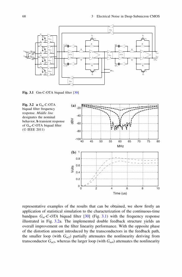
representative examples of the results that can be obtained, we show firstly anapplication of statistical simulation to the characterization of the continuous-timebandpass Gm-C-OTA biquad filter [30] (Fig. 3.1) with the frequency responseillustrated in Fig. 3.2a. The implemented double feedback structure yields anoverall improvement on the filter linearity performance. With the opposite phaseof the distortion amount introduced by the transconductors in the feedback path,the smaller loop (with Gm2) partially attenuates the nonlinearity deriving fromtransconductor Gm3, whereas the larger loop (with Gm4) attenuates the nonlinearity
Fig. 3.1 Gm-C-OTA biquad filter [30]
40 45 50 55 60 65 70 75 80-100
-80
-60
-40
-20
dBV
MHz
0 2 4 6 8 100
0.2
0.4
0.6
0.8
1
Vol
ts
Time (us)
(a)
(b)
Fig. 3.2 a Gm-C-OTAbiquad filter frequencyresponse. Middle linedesignates the nominalbehavior, b transient responseof Gm-C-OTA biquad filter(� IEEE 2011)
68 3 Electrical Noise in Deep-Submicron CMOS
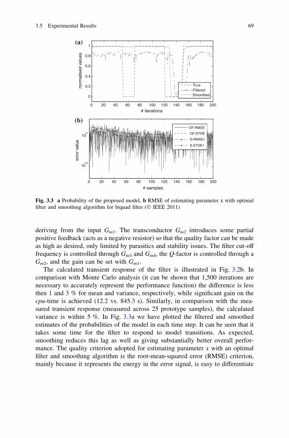
deriving from the input Gm1. The transconductor Gm2 introduces some partialpositive feedback (acts as a negative resistor) so that the quality factor can be madeas high as desired, only limited by parasitics and stability issues. The filter cut-offfrequency is controlled through Gm3 and Gm4, the Q-factor is controlled through aGm2, and the gain can be set with Gm1.
The calculated transient response of the filter is illustrated in Fig. 3.2b. Incomparison with Monte Carlo analysis (it can be shown that 1,500 iterations arenecessary to accurately represent the performance function) the difference is lessthen 1 and 3 % for mean and variance, respectively, while significant gain on thecpu-time is achieved (12.2 vs. 845.3 s). Similarly, in comparison with the mea-sured transient response (measured across 25 prototype samples), the calculatedvariance is within 5 %. In Fig. 3.3a we have plotted the filtered and smoothedestimates of the probabilities of the model in each time step. It can be seen that ittakes some time for the filter to respond to model transitions. As expected,smoothing reduces this lag as well as giving substantially better overall perfor-mance. The quality criterion adopted for estimating parameter x with an optimalfilter and smoothing algorithm is the root-mean-squared error (RMSE) criterion,mainly because it represents the energy in the error signal, is easy to differentiate
0 20 40 60 80 100 120 140 160 180 200
0
0.2
0.4
0.6
0.8
1
# iterations
norm
alis
ed v
alue
sTrueFilteredSmoothed
0 20 40 60 80 100 120 140 160 180 200
10-10
10-5
# samples
erro
r va
lue
OF-RMSE
OF-STDE
S-RMSE1
S-STDE1
(a)
(b)
Fig. 3.3 a Probability of the proposed model, b RMSE of estimating parameter x with optimalfilter and smoothing algorithm for biquad filter (� IEEE 2011)
3.5 Experimental Results 69
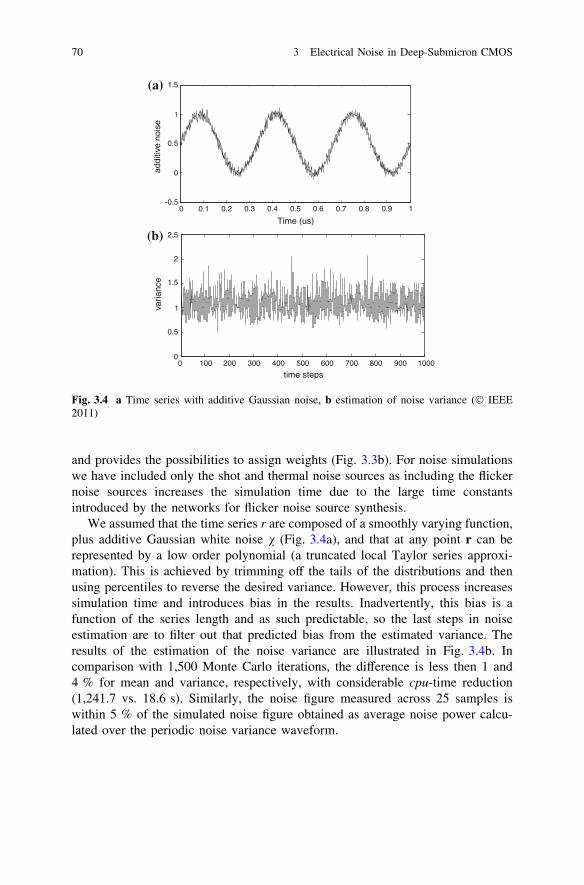
and provides the possibilities to assign weights (Fig. 3.3b). For noise simulationswe have included only the shot and thermal noise sources as including the flickernoise sources increases the simulation time due to the large time constantsintroduced by the networks for flicker noise source synthesis.
We assumed that the time series r are composed of a smoothly varying function,plus additive Gaussian white noise v (Fig. 3.4a), and that at any point r can berepresented by a low order polynomial (a truncated local Taylor series approxi-mation). This is achieved by trimming off the tails of the distributions and thenusing percentiles to reverse the desired variance. However, this process increasessimulation time and introduces bias in the results. Inadvertently, this bias is afunction of the series length and as such predictable, so the last steps in noiseestimation are to filter out that predicted bias from the estimated variance. Theresults of the estimation of the noise variance are illustrated in Fig. 3.4b. Incomparison with 1,500 Monte Carlo iterations, the difference is less then 1 and4 % for mean and variance, respectively, with considerable cpu-time reduction(1,241.7 vs. 18.6 s). Similarly, the noise figure measured across 25 samples iswithin 5 % of the simulated noise figure obtained as average noise power calcu-lated over the periodic noise variance waveform.
0 0.1 0.2 0.3 0.4 0.5 0.6 0.7 0.8 0.9 1-0.5
0
0.5
1
1.5
Time (us)
addi
tive
nois
e
0 100 200 300 400 500 600 700 800 900 10000
0.5
1
1.5
2
2.5
time steps
varia
nce
(a)
(b)
Fig. 3.4 a Time series with additive Gaussian noise, b estimation of noise variance (� IEEE2011)
70 3 Electrical Noise in Deep-Submicron CMOS
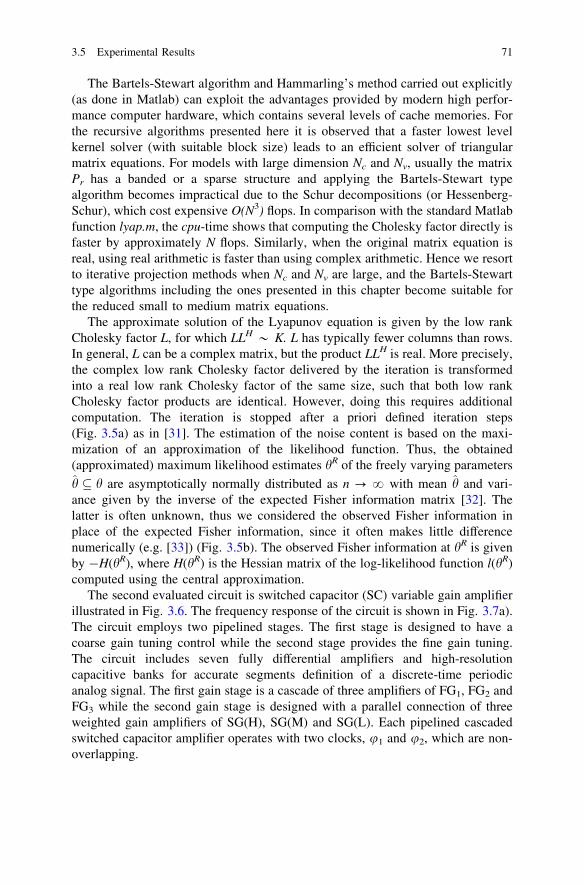
The Bartels-Stewart algorithm and Hammarling’s method carried out explicitly(as done in Matlab) can exploit the advantages provided by modern high perfor-mance computer hardware, which contains several levels of cache memories. Forthe recursive algorithms presented here it is observed that a faster lowest levelkernel solver (with suitable block size) leads to an efficient solver of triangularmatrix equations. For models with large dimension Nc and Nv, usually the matrixPr has a banded or a sparse structure and applying the Bartels-Stewart typealgorithm becomes impractical due to the Schur decompositions (or Hessenberg-Schur), which cost expensive O(N3) flops. In comparison with the standard Matlabfunction lyap.m, the cpu-time shows that computing the Cholesky factor directly isfaster by approximately N flops. Similarly, when the original matrix equation isreal, using real arithmetic is faster than using complex arithmetic. Hence we resortto iterative projection methods when Nc and Nv are large, and the Bartels-Stewarttype algorithms including the ones presented in this chapter become suitable forthe reduced small to medium matrix equations.
The approximate solution of the Lyapunov equation is given by the low rankCholesky factor L, for which LLH * K. L has typically fewer columns than rows.In general, L can be a complex matrix, but the product LLH is real. More precisely,the complex low rank Cholesky factor delivered by the iteration is transformedinto a real low rank Cholesky factor of the same size, such that both low rankCholesky factor products are identical. However, doing this requires additionalcomputation. The iteration is stopped after a priori defined iteration steps(Fig. 3.5a) as in [31]. The estimation of the noise content is based on the maxi-mization of an approximation of the likelihood function. Thus, the obtained(approximated) maximum likelihood estimates hR of the freely varying parameters
h � h are asymptotically normally distributed as n ? ? with mean h and vari-ance given by the inverse of the expected Fisher information matrix [32]. Thelatter is often unknown, thus we considered the observed Fisher information inplace of the expected Fisher information, since it often makes little differencenumerically (e.g. [33]) (Fig. 3.5b). The observed Fisher information at hR is givenby -H(hR), where H(hR) is the Hessian matrix of the log-likelihood function l(hR)computed using the central approximation.
The second evaluated circuit is switched capacitor (SC) variable gain amplifierillustrated in Fig. 3.6. The frequency response of the circuit is shown in Fig. 3.7a).The circuit employs two pipelined stages. The first stage is designed to have acoarse gain tuning control while the second stage provides the fine gain tuning.The circuit includes seven fully differential amplifiers and high-resolutioncapacitive banks for accurate segments definition of a discrete-time periodicanalog signal. The first gain stage is a cascade of three amplifiers of FG1, FG2 andFG3 while the second gain stage is designed with a parallel connection of threeweighted gain amplifiers of SG(H), SG(M) and SG(L). Each pipelined cascadedswitched capacitor amplifier operates with two clocks, u1 and u2, which are non-overlapping.
3.5 Experimental Results 71
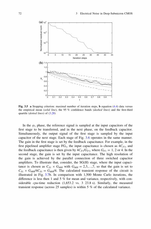
In the u1 phase, the reference signal is sampled at the input capacitors of thefirst stage to be transferred, and in the next phase, on the feedback capacitor.Simultaneously, the output signal of the first stage is sampled by the inputcapacitor of the next stage. Each stage of Fig. 3.6 operates in the same manner.The gain in the first stage is set by the feedback capacitance. For example, in thefirst pipelined amplifier stage FG1, the input capacitance is chosen as 4CF1, andthe feedback capacitance is then given by 4CF1/GF1, where GF1 = 1, 2 or 4. In thesecond stage, the gain is set by the input capacitance. The high resolution ofthe gain is achieved by the parallel connection of three switched capacitoramplifiers. To illustrate that, consider, the SG(H) stage, where the input capaci-tance is chosen as CS1 9 GMH with GMH = 2,3,…,7, so that the gain is set toCS1 9 GMH/4CS1 = GMH/4. The calculated transient response of the circuit isillustrated in Fig. 3.7b. In comparison with 1,500 Monte Carlo iterations, thedifference is less then 1 and 5 % for mean and variance, respectively, with con-siderable cpu-time reduction (1,653.2 vs. 3 23.8 s). Similarly, the measuredtransient response (across 25 samples) is within 5 % of the calculated variance.
0 5 10 15 20 25 30 35 40 4510-15
10-10
10-5
100
Nor
mal
ized
res
idua
l nor
m
Iteration steps
0 0.1 0.2 0.3 0.4 0.5 0.6 0.7 0.8 0.9 10
0.2
0.4
0.6
0.8
1
1.2
1.4
t
Xt
(a)
(b)
Fig. 3.5 a Stopping criterion: maximal number of iteration steps, b equation (4.4) data versusthe empirical mean (solid line), the 95 % confidence bands (dashed lines) and the first-thirdquartile (dotted lines) of (3.28)
72 3 Electrical Noise in Deep-Submicron CMOS
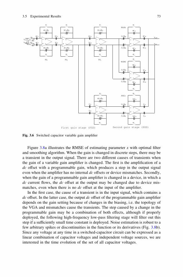
Figure 3.8a illustrates the RMSE of estimating parameter x with optimal filterand smoothing algorithm. When the gain is changed in discrete steps, there may bea transient in the output signal. There are two different causes of transients whenthe gain of a variable gain amplifier is changed. The first is the amplification of adc offset with a programmable gain, which produces a step in the output signaleven when the amplifier has no internal dc offsets or device mismatches. Secondly,when the gain of a programmable gain amplifier is changed in a device, in which adc current flows, the dc offset at the output may be changed due to device mis-matches, even when there is no dc offset at the input of the amplifier.
In the first case, the cause of a transient is in the input signal, which contains adc offset. In the latter case, the output dc offset of the programmable gain amplifierdepends on the gain setting because of changes in the biasing, i.e. the topology ofthe VGA and mismatches cause the transients. The step caused by a change in theprogrammable gain may be a combination of both effects, although if properlydeployed, the following high-frequency low-pass filtering stage will filter out thisstep if a sufficiently small time constant is deployed. Noise estimation is robust to afew arbitrary spikes or discontinuities in the function or its derivatives (Fig. 3.8b).Since any voltage at any time in a switched-capacitor circuit can be expressed as alinear combination of capacitor voltages and independent voltage sources, we areinterested in the time evolution of the set of all capacitor voltages.
Fig. 3.6 Switched capacitor variable gain amplifier
3.5 Experimental Results 73
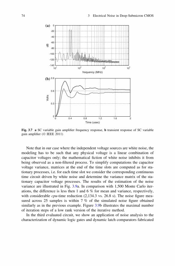
Note that in our case where the independent voltage sources are white noise, themodeling has to be such that any physical voltage is a linear combination ofcapacitor voltages only; the mathematical fiction of white noise inhibits it frombeing observed as a non-filtered process. To simplify computations the capacitorvoltage variance, matrices at the end of the time slots are computed as for sta-tionary processes, i.e. for each time slot we consider the corresponding continuoustime circuit driven by white noise and determine the variance matrix of the sta-tionary capacitor voltage processes. The results of the estimation of the noisevariance are illustrated in Fig. 3.9a. In comparison with 1,500 Monte Carlo iter-ations, the difference is less then 1 and 6 % for mean and variance, respectively,with considerable cpu-time reduction (2,134.3 vs. 26.8 s). The noise figure mea-sured across 25 samples is within 7 % of the simulated noise figure obtainedsimilarly as in the previous example. Figure 3.9b illustrates the maximal numberof iteration steps of a low rank version of the iterative method.
In the third evaluated circuit, we show an application of noise analysis to thecharacterization of dynamic logic gates and dynamic latch comparators fabricated
101
102
103
104
-140
-120
-100
-80
-60
-40
-20
0
frequency (MHz)
dB
0 0.4 0.8 1.2 1.6 20
0.3
0.6
0.9
Vol
ts
Time (usec)
(a)
(b)
Fig. 3.7 a SC variable gain amplifier frequency response, b transient response of SC variablegain amplifier (� IEEE 2011)
74 3 Electrical Noise in Deep-Submicron CMOS
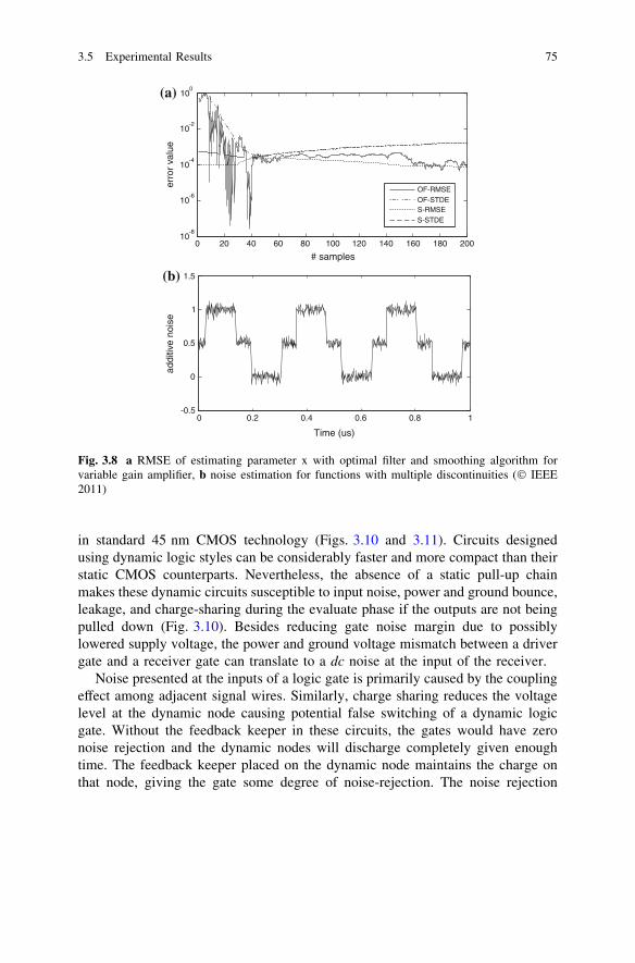
in standard 45 nm CMOS technology (Figs. 3.10 and 3.11). Circuits designedusing dynamic logic styles can be considerably faster and more compact than theirstatic CMOS counterparts. Nevertheless, the absence of a static pull-up chainmakes these dynamic circuits susceptible to input noise, power and ground bounce,leakage, and charge-sharing during the evaluate phase if the outputs are not beingpulled down (Fig. 3.10). Besides reducing gate noise margin due to possiblylowered supply voltage, the power and ground voltage mismatch between a drivergate and a receiver gate can translate to a dc noise at the input of the receiver.
Noise presented at the inputs of a logic gate is primarily caused by the couplingeffect among adjacent signal wires. Similarly, charge sharing reduces the voltagelevel at the dynamic node causing potential false switching of a dynamic logicgate. Without the feedback keeper in these circuits, the gates would have zeronoise rejection and the dynamic nodes will discharge completely given enoughtime. The feedback keeper placed on the dynamic node maintains the charge onthat node, giving the gate some degree of noise-rejection. The noise rejection
0 20 40 60 80 100 120 140 160 180 20010
-8
10-6
10-4
10-2
100
# samples
erro
r va
lue
OF-RMSEOF-STDES-RMSES-STDE
0 0.2 0.4 0.6 0.8 1-0.5
0
0.5
1
1.5
Time (us)
addi
tive
nois
e
(a)
(b)
Fig. 3.8 a RMSE of estimating parameter x with optimal filter and smoothing algorithm forvariable gain amplifier, b noise estimation for functions with multiple discontinuities (� IEEE2011)
3.5 Experimental Results 75
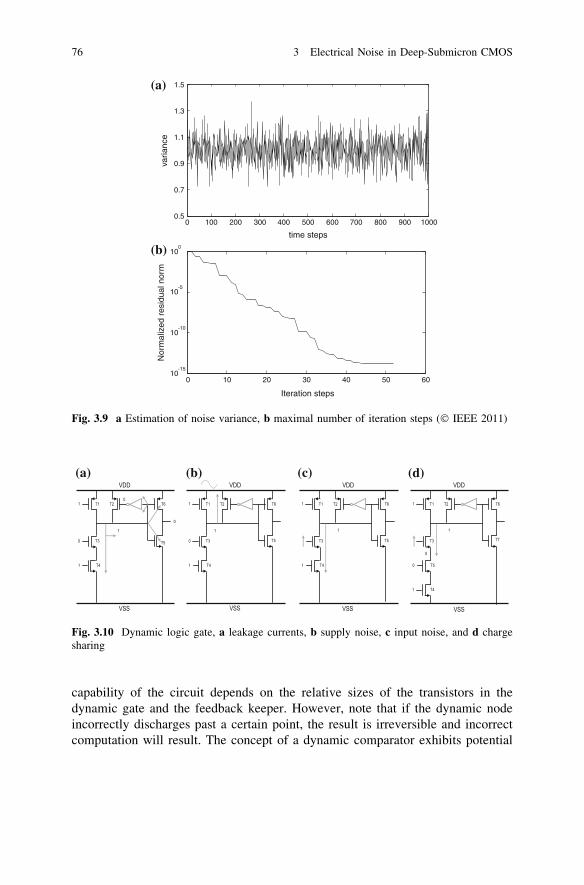
capability of the circuit depends on the relative sizes of the transistors in thedynamic gate and the feedback keeper. However, note that if the dynamic nodeincorrectly discharges past a certain point, the result is irreversible and incorrectcomputation will result. The concept of a dynamic comparator exhibits potential
0 100 200 300 400 500 600 700 800 900 10000.5
0.7
0.9
1.1
1.3
1.5
time steps
varia
nce
0 10 20 30 40 50 6010
-15
10-10
10-5
100
Nor
mal
ized
res
idua
l nor
m
Iteration steps
(a)
(b)
Fig. 3.9 a Estimation of noise variance, b maximal number of iteration steps (� IEEE 2011)
(a) (b) (c) (d)
Fig. 3.10 Dynamic logic gate, a leakage currents, b supply noise, c input noise, and d chargesharing
76 3 Electrical Noise in Deep-Submicron CMOS
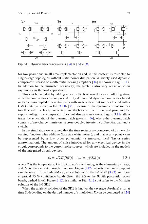
for low power and small area implementation and, in this context, is restricted tosingle-stage topologies without static power dissipation. A widely used dynamiccomparator is based on a differential sensing amplifier [34] as shown in Fig. 3.11a.In addition to the mismatch sensitivity, the latch is also very sensitive to anasymmetry in the load capacitance.
This can be avoided by adding an extra latch or inverters as a buffering stageafter the comparator core outputs. A fully differential dynamic comparator basedon two cross-coupled differential pairs with switched current sources loaded with aCMOS latch is shown in Fig. 3.11b [35]. Because of the dynamic current sourcestogether with the latch, connected directly between the differential pairs and thesupply voltage, the comparator does not dissipate dc-power. Figure 3.11c illus-trates the schematic of the dynamic latch given in [36], where the dynamic latchconsists of pre-charge transistors, a cross-coupled inverter, a differential pair and aswitch.
In the simulation we assumed that the time series x are composed of a smoothlyvarying function, plus additive Gaussian white noise n, and that at any point x canbe represented by a low order polynomial (a truncated local Taylor seriesapproximation). The amount of noise introduced for any electrical device in thecircuit corresponds to the current noise sources, which are included in the modelsof the integrated-circuit devices
ith ¼ffiffiffiffiffiffiffiffiffiffiffiffiffi2kT=R
pnðtÞ ishot ¼
ffiffiffiffiffiffiffiffiffiqeIDp
nðtÞ ð3:34Þ
where T is the temperature, k is Boltzmann’s constant, qe is the elementary charge,and ID is the current through junction. Figure 3.12a reports the point-by-pointsample mean of the Euler–Maruyama solutions of the Itô SDE (3.23) and theirempirical 95 % confidence bands (from the 2.5 to the 97.5th percentile; outerbands, dashed lines). Figure 3.12b is similar as Fig. 3.12a but refers to the Milsteinsolution of the Itô SDE.
When the analytic solution of the SDE is known, the (average absolute) error attime T, depending on the desired number of simulations R, can be computed as [24]
(a) (b) (c)
Fig. 3.11 Dynamic latch comparators, a [34], b [35], c [36]
3.5 Experimental Results 77
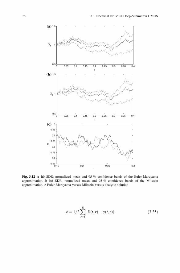
e ¼ 1=2XR
r¼1
Xðt; rÞ � yðt; rÞj j ð3:35Þ
0 0.05 0.1 0.15 0.2 0.25 0.3 0.35 0.40.5
1
1.5
t
Xt
Xt
Xt
0 0.05 0.1 0.15 0.2 0.25 0.3 0.35 0.40.5
1
1.5
t
0.15 0.2 0.25 0.30.65
0.7
0.75
0.8
0.85
0.9
0.95
1
t
(a)
(b)
(c)
Fig. 3.12 a Itô SDE: normalized mean and 95 % confidence bands of the Euler-Maruyamaapproximation, b Itô SDE: normalized mean and 95 % confidence bands of the Milsteinapproximation, c Euler-Maruyama versus Milstein versus analytic solution
78 3 Electrical Noise in Deep-Submicron CMOS

where X(t, r) and y(t, r) denote the value of the analytic solution at time t in the rthtrajectory and the value of the numerical solution for the chosen approximationscheme at time t in the rth trajectory, respectively. Figure 3.12c compare theEuler–Maruyama solutions (dotted lines) of the Itô SDE with the correspondingadapted Milstein solutions (solid lines) and the analytic solutions (dashed lines):the adapted Milstein and the analytic solutions are so close that they appearpractically undistinguishable. For the calculation of the error, the analytic solutionand the numerical solution must be computed on the same Brownian path (i.e.using the same sequence of pseudorandom numbers). At time T = 1 the Euler–Maruyama method for the Itô SDE implies an average error equals to1.048 9 10-2, while the adapted Milstein scheme for the Itô SDE implies anaverage error of 5.962 9 10-5. These results show that the Milstein method ismore accurate, although the Euler–Maruyama method is faster: 27 and 11 % incomparison with classical Milstein method and proposed adapted Milstein method,respectively. Descriptive statistics are reported with respect to the simulated valuesat the endpoint t: e.g. for the Euler-Maruyama approximation of the Itô SDE wehave, E(Xt) & 1.161 where E(.) denotes expectation, Var(Xt) & 0.367,
0 100 200 300 400 500 600 700 800 900 1000
0.7
0.8
0.9
1
1.1
1.2
1.3
1.4
1.5
time steps
varia
nce
0 2 4 6 8 10 12 14 16 18 2010
-2
10-1
100
Nor
mal
ized
res
idua
l nor
m
Iteration steps
(a)
(b)
Fig. 3.13 a Estimation of noise variance, b stopping criterion: maximal number of iteration steps
3.5 Experimental Results 79
Median(Xt) = 1.029, etc. One example of the estimated noise variance (obtainedat the output node of the dynamic logic gate) is illustrated in Fig. 3.13a. Incomparison with 1,500 Monte Carlo iterations, at any of the circuit nodes, thedifference is less then 1.1 and 3.2 % for mean and variance, respectively, whileachieving considerable cpu-time reduction (32.4 vs. 2.1 s).
Similarly, for dynamic latch comparators [34–36], the difference is less than1.1, 1.0 and 1.1 % for mean, and 2.9, 3.1 and 3.0 % for variance, respectively.Correspondingly, the achieved speed gain is 14, 16 and 15 times. For the adaptedMilstein method, in comparison with 1,500 Monte Carlo iterations, the differencefor dynamic logic gate is less than 0.2 and 0.8 % for mean and variance,respectively, with 14 times cpu-time reduction. Similarly, the achieved speed gainsfor dynamic latch comparators [34–36] are 12, 14 and 13 times, while the precisionis within 0.3, 0.2 and 0.3 % for mean, and 0.7, 0.9 and 0.8 % for variance.Consequently, the adapted Milstein method realizes three times speed increase incomparison with classical Milstein method. The low rank Cholesky factor iterationis stopped after a priori defined iteration steps (Fig. 3.13b).
3.6 Conclusions
In addition to the process variation variability, statistical simulation affected withcircuit noise is one of the foremost steps in the evaluation of successful high-performance IC designs. As circuit noise is modeled as non-stationary process, Itôstochastic differentials are introduced as a convenient way to represent such aprocess. Two adaptive deterministic numerical integration methods, namely, theEuler-Maruyama and adapted Milstein schemes, are proposed to find a numericalsolution of Itô differential equations. Additionally, an effective numerical solutionfor a set of linear time-varying equations defining the variance-covariance matrixis found. To examine simulation accuracy, time varying voltage nodes and currentbranches are formulated as stochastic state space models, and the time evolution ofthe system is estimated using optimal filters. The state transitions are modeled as aMarkovian switching system, which is perturbed by a certain process noise.
Furthermore, a discrete recursive algorithm is described to accurately estimatenoise contributions of individual electrical quantities. This makes it possible forthe designer to evaluate the devices that most affect a particular performance, sothat design efforts can be addressed to the most critical section of the circuit. Asthe results indicate, the suggested numerical method provides an accurate andefficient solution.
The effectiveness of the described approaches was evaluated on severaldynamic circuits with the continuous-time bandpass biquad filter and the discrete-time variable gain amplifier as representative examples. As the results indicate, thesuggested numerical method provides accurate and efficient solutions of stochasticdifferentials for noise analysis.
80 3 Electrical Noise in Deep-Submicron CMOS

References
1. R. Rohrer, L. Nagel, R.G. Meyer, L. Weber, Computationally efficient electronic-circuitnoise calculations. IEEE J. Solid-State Circuits 6, 204–213 (1971)
2. C.D. Hull, R.G. Meyer, A systematic approach to the analysis of noise in mixers. IEEE Trans.Circuits Syst. I 40, 909–919 (1993)
3. M. Okumura, H. Tanimoto, T. Itakura, T. Sugawara, Numerical noise analysis for nonlinearcircuits with a periodic large signal excitation including cyclostationary noise sources. IEEETrans. Circuits Syst. I 40, 581–590 (1993)
4. P. Bolcato, R. Poujois, A new approach for noise simulation in transient analysis, inProceedings of IEEE International Symposium on Circuits and Systems, 1992
5. A. Demir, E. Liu, A. Sangiovanni-Vincentelli, Time-domain non-Monte Carlo noisesimulation for nonlinear dynamic circuits with arbitrary excitations, in Proceedings of IEEEInternational Conference on Computer Aided Design, 1994, pp. 598–603
6. J.-M. Sanz-Serna, Numerical Ordinary Differential Equations Versus Dynamical Systems, ed.by D.S. Broomhead, A. Iserles. The dynamics of numerics and the numerics of dynamics(Clarendon Press, Oxford, 1992)
7. P.R. Gray, R.G. Meyer, Analysis and Design Of Analog Integrated Circuits (Wiley, NewYork, 1984)
8. L. Arnold, Stochastic Differential Equations: Theory and Application (Wiley, New York,1974)
9. A. Sangiovanni-Vincentelli, ‘‘Circuit Simulation’’ in Computer Design Aids for VLSI Circuits(Sijthoff and Noordhoff, The Netherlands, 1980)
10. P. Heydari, M. Pedram, Model-order reduction using variational balanced truncation withspectral shaping. IEEE Trans. Circuits Syst. I Regul. Pap. 53(4), 879–891 (2006)
11. M. Di Marco, M. Forti, M. Grazzini, P. Nistri, L. Pancioni, Lyapunov method andconvergence of the full-range model of CNNs. IEEE Trans. Circuits Syst. I Regul. Pap.55(11), 3528–3541 (2008)
12. K.H. Lim, K.P. Seng, L.-M. Ang, S.W. Chin, Lyapunov theory-based multilayered neuralnetwork. IEEE Trans. Circuits Syst. II Express Briefs 56(4), 305–309 (2009)
13. X. Liu, Stability analysis of switched positive systems: a switched linear copositiveLyapunov function method. IEEE Trans. Circuits Syst. II Express Briefs 56(5), 414–418(2009)
14. R.H. Bartels, G.W. Stewart, Solution of the matrix equation AX ? XB = C. Commun.Assoc. Comput. Mach. 15, 820–826 (1972)
15. N.J. Higham, Perturbation theory and backward error for AX - XB = C. BIT Numer. Math.33, 124–136 (1993)
16. T. Penzl, Numerical solution of generalized Lyapunov equations. Adv. Comput. Math 8,33–48 (1998)
17. G.H. Golub, C.F. van Loan, Matrix Computations (Johns Hopkins University Press,Baltimore, 1996)
18. I. Jaimoukha, E. Kasenally, Krylov subspace methods for solving large Lyapunov equations.SIAM J. Numer. Anal. 31, 227–251 (1994)
19. E. Wachspress, Iterative solution of the Lyapunov matrix equation. Appl. Math. Lett. 1,87–90 (1998)
20. J. Li, F. Wang, J. White, An efficient Lyapunov equation-based approach for generatingreduced-order models of interconnect, in Proceedings of IEEE Design AutomationConference, 1999, pp. 1–6
21. T.L. Chen, G. Gildenblat, Symmetric bulk charge linearization in the charge-sheet model.IEEE Electr. Lett. 37, 791–793 (2001)
22. R. van Langevelde, A.J. Scholten, D.B.M. Klassen, MOS model 11: level 1102, PhilipsResearch Technical Report 2004/85, http://www.nxp.com/models/mos_models/model11/
References 81

23. J. Vlach, K. Singhal, Computer methods for circuit analysis and design (Van NostrandReinhold, New York, 1983)
24. P.E. Kloeden, E. Platen, H. Schurz, Numerical Solution of SDE Through ComputerExperiments (Springer, Berlin, 1994)
25. W. Romisch, R. Winkler, Stepsize control for mean-square numerical methods for stochasticdifferential equations with small noise. SIAM J. Sci. Comput. 28, 604–625 (2006)
26. L. Grune, P.E. Kloeden, Pathwise approximation of random ordinary differential equations.BIT Numer. Math. 41(4), 711–721 (2001)
27. I. Gyongy, A note on Euler’s approximations. Potential Anal. 8(3), 205–216 (1998)28. A.S. Hurn, K.A. Lindsay, V.L. Martin, On the efficacy of simulated ML for estimating the
parameters of SDEs. J. Time Ser. Anal. 24(1), 45–63 (2003)29. MatLab, http://www.mathworks.com/30. A. Zjajo, M. Song, Digitally programmable continuous-time biquad filter in 65-nm CMOS, in
Proceedings of IEEE International Symposium on Radio-Frequency Integration Technology,2009, pp. 339–342
31. The numerics in control network, http://www.win.tue.nl/wgs/niconet.html32. D. Dacunha-Castelle, D. Florens-Zmirnou, Estimation of the coefficients of a diffusion from
discrete observations. Stochastics 19, 263–284 (1986)33. O.E. Barndorff-Nielsen, M. Sørensen, A review of some aspects of asymptotic likelihood
theory for stochastic processes. Int. Stat. Rev. 62(1), 133–165 (1994)34. T.B. Cho, P.R. Gray, A 10 b, 20 Msample/s, 35 mW pipeline A/D converter. IEEE J. Solid-
State Circuits 30(3), 166–172 (1995)35. L. Sumanen, M. Waltari, K. Halonen, A mismatch insensitive CMOS dynamic comparator
for pipeline A/D converters, in Proceedings of the IEEE International Conference on Circuitsand Systems, 2000, pp. 32–35
36. T. Kobayashi, K. Nogami, T. Shirotori, Y. Fujimoto, A current controlled latch senseamplifier and a static power-saving input buffer for low-power architecture. IEEE J. Solid-State Circuits 28(4), 523–527 (1993)
82 3 Electrical Noise in Deep-Submicron CMOS
Chapter 4Temperature Effects in Deep-SubmicronCMOS
In the nanometer regime, the transistor scaling has been slowing down due to the
challenges and hindrances of increasing variability, short-channel effects, power/
thermal problems and the complexity of interconnect. The 3D integration has been
proposed as one of the alternatives to overcome the interconnect restrictions [1].
However, thermal management is of critical importance for 3D IC designs [2] due
to the degradation of performance and reliability [3]. Heat and thermal problems
are exacerbated for 3D applications as the vertically stacked multiple layers of
active devices cause a rapid increase of power density. Higher temperature
increases the risk of damaging the devices and interconnects (since major back-end
and front-end reliability issues including electromigration, time-dependent
dielectric breakdown, and negative-bias temperature instability have strong
dependence on temperature), even with advanced thermal management technol-
ogies [4]. The complexity of the interconnection structures, back end of line
structures and through-silicon vias increase the complexity of the conductive heat
transfer paths in a stacked die structure. Dummy vias and inter-tier connections
can be used to increase the vertical heat transfer through the stack and reduce the
temperature peaks in the die [5].
Successful application of 3D integration requires analysis of thermal manage-
ment problem, and the development of an analytical model for heat transport in 3D
ICs to establish thermal design rules governing the feasibility of integration
options. A thermal analysis of heterogeneous 3D ICs with various integration
schemes has been presented in [6]. The analysis of temperature distribution on an
inhomogeneous substrate layer is performed employing finite-difference time
domain [7], based on the image method [8], neural networks [9], green function
[10], fast Hankel transform of green function [11], or mesh based methods [12].
However, existing thermal-simulation methods, when applied to a full-chip, reduce
the computational complexity of the problem by homogenizing the materials
within a layer, limiting the extent of an eigenfunction expansion, or ignoring
sources’ proximity to boundaries. These simplifications render their results less
accurate at fine length-scales, on wires, vias, or individual transistors. Accurate
computation of temperature at the length-scales of devices and interconnects
requires the development of a fundamental analytical model for heat transport in
A. Zjajo, Stochastic Process Variation in Deep-Submicron CMOS, Springer Seriesin Advanced Microelectronics 48, DOI: 10.1007/978-94-007-7781-1_4,
� Springer Science+Business Media Dordrecht 2014
83
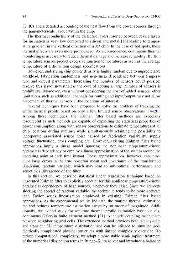
3D ICs and a detailed accounting of the heat flow from the power sources through
the nanometerscale layout within the chip.
The thermal conductivity of the dielectric layers inserted between device layers
for insulation is very low compared to silicon and metal [13] leading to temper-
ature gradient in the vertical direction of a 3D chip. In the case of hot spots, these
thermal effects are even more pronounced. As a consequence, continuous thermal
monitoring is necessary to reduce thermal damage and increase reliability. Built-in
temperature sensors predict excessive junction temperatures as well as the average
temperature of a die within design specifications.
However, underlying chip power density is highly random due to unpredictable
workload, fabrication randomness and non-linear dependence between tempera-
ture and circuit parameters. Increasing the number of sensors could possible
resolve this issue; nevertheless the cost of adding a large number of sensors is
prohibitive. Moreover, even without considering the cost of added sensors, other
limitations such as additional channels for routing and input/output may not allow
placement of thermal sensors at the locations of interest.
Several techniques have been proposed to solve the problem of tracking the
entire thermal profile based on only a few limited sensor observations [14–20].
Among these techniques, the Kalman filter based methods are especially
resourceful as such methods are capable of exploiting the statistical properties of
power consumption along with sensor observations to estimate temperatures at all
chip locations during runtime, while simultaneously retaining the possibility to
incorporate associated sensor noise caused by fabrication variability, supply
voltage fluctuation, cross coupling etc. However, existing Kalman filter based
approaches imply a linear model ignoring the nonlinear temperature-circuit
parameters dependency or employ a linear approximation of the system around the
operating point at each time instant. These approximations, however, can intro-
duce large errors in the true posterior mean and covariance of the transformed
(Gaussian) random variable, which may lead to sub-optimal performance and
sometimes divergence of the filter.
In this section, we describe statistical linear regression technique based on
unscented Kalman filter to explicitly account for this nonlinear temperature-circuit
parameters dependency of heat sources, whenever they exist. Since we are con-
sidering the spread of random variable, the technique tends to be more accurate
than Taylor series linearization employed in existing Kalman filter based
approaches. As the experimental results indicate, the runtime thermal estimation
method reduces temperature estimation errors by an order of magnitude. Addi-
tionally, we extend study for accurate thermal profile estimation based on dis-
continuous Galerkin finite element method [21] to include coupling mechanism
between neighboring grid cells. The extended method provides both, steady-state
and transient 3D temperature distribution and can be utilized to simulate geo-
metrically complicated physical structures with limited complexity overhead. To
reduce computational complexity, we adopt a more stable semi-implicit treatment
of the numerical dissipation terms in Runge–Kutta solver and introduce a balanced
84 4 Temperature Effects in Deep-Submicron CMOS
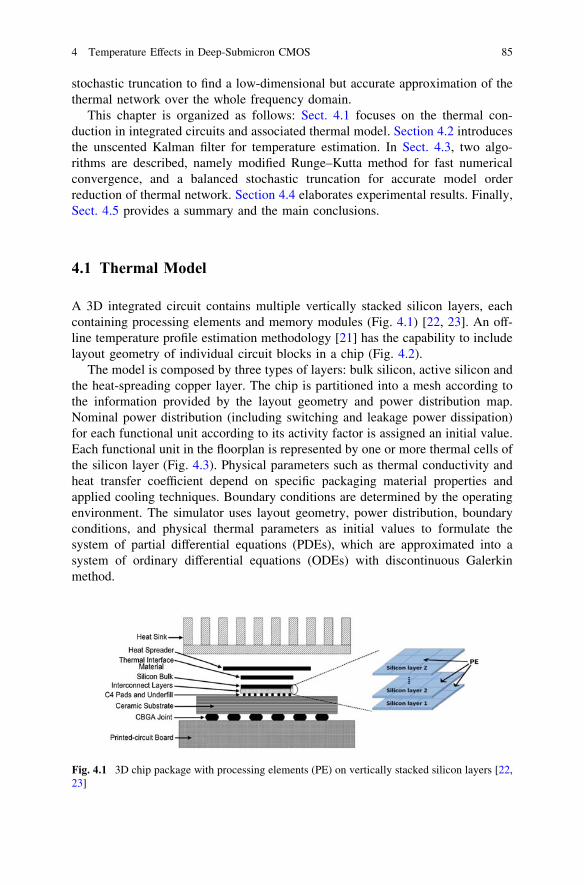
stochastic truncation to find a low-dimensional but accurate approximation of the
thermal network over the whole frequency domain.
This chapter is organized as follows: Sect. 4.1 focuses on the thermal con-
duction in integrated circuits and associated thermal model. Section 4.2 introduces
the unscented Kalman filter for temperature estimation. In Sect. 4.3, two algo-
rithms are described, namely modified Runge–Kutta method for fast numerical
convergence, and a balanced stochastic truncation for accurate model order
reduction of thermal network. Section 4.4 elaborates experimental results. Finally,
Sect. 4.5 provides a summary and the main conclusions.
4.1 Thermal Model
A 3D integrated circuit contains multiple vertically stacked silicon layers, each
containing processing elements and memory modules (Fig. 4.1) [22, 23]. An off-
line temperature profile estimation methodology [21] has the capability to include
layout geometry of individual circuit blocks in a chip (Fig. 4.2).
The model is composed by three types of layers: bulk silicon, active silicon and
the heat-spreading copper layer. The chip is partitioned into a mesh according to
the information provided by the layout geometry and power distribution map.
Nominal power distribution (including switching and leakage power dissipation)
for each functional unit according to its activity factor is assigned an initial value.
Each functional unit in the floorplan is represented by one or more thermal cells of
the silicon layer (Fig. 4.3). Physical parameters such as thermal conductivity and
heat transfer coefficient depend on specific packaging material properties and
applied cooling techniques. Boundary conditions are determined by the operating
environment. The simulator uses layout geometry, power distribution, boundary
conditions, and physical thermal parameters as initial values to formulate the
system of partial differential equations (PDEs), which are approximated into a
system of ordinary differential equations (ODEs) with discontinuous Galerkin
method.
Fig. 4.1 3D chip package with processing elements (PE) on vertically stacked silicon layers [22,
23]
4 Temperature Effects in Deep-Submicron CMOS 85
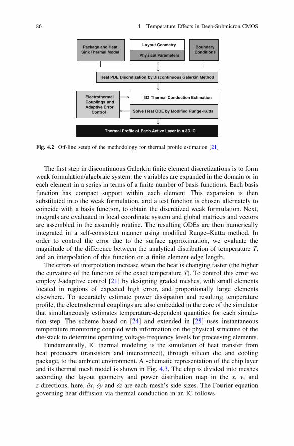
The first step in discontinuous Galerkin finite element discretizations is to form
weak formulation/algebraic system: the variables are expanded in the domain or in
each element in a series in terms of a finite number of basis functions. Each basis
function has compact support within each element. This expansion is then
substituted into the weak formulation, and a test function is chosen alternately to
coincide with a basis function, to obtain the discretized weak formulation. Next,
integrals are evaluated in local coordinate system and global matrices and vectors
are assembled in the assembly routine. The resulting ODEs are then numerically
integrated in a self-consistent manner using modified Runge–Kutta method. In
order to control the error due to the surface approximation, we evaluate the
magnitude of the difference between the analytical distribution of temperature T,and an interpolation of this function on a finite element edge length.
The errors of interpolation increase when the heat is changing faster (the higher
the curvature of the function of the exact temperature T). To control this error we
employ l-adaptive control [21] by designing graded meshes, with small elements
located in regions of expected high error, and proportionally large elements
elsewhere. To accurately estimate power dissipation and resulting temperature
profile, the electrothermal couplings are also embedded in the core of the simulator
that simultaneously estimates temperature-dependent quantities for each simula-
tion step. The scheme based on [24] and extended in [25] uses instantaneous
temperature monitoring coupled with information on the physical structure of the
die-stack to determine operating voltage-frequency levels for processing elements.
Fundamentally, IC thermal modeling is the simulation of heat transfer from
heat producers (transistors and interconnect), through silicon die and cooling
package, to the ambient environment. A schematic representation of the chip layer
and its thermal mesh model is shown in Fig. 4.3. The chip is divided into meshes
according the layout geometry and power distribution map in the x, y, and
z directions, here, δx, δy and δz are each mesh’s side sizes. The Fourier equation
governing heat diffusion via thermal conduction in an IC follows
Package and Heat Sink Thermal Model
Layout Geometry
Physical Parameters
Boundary Conditions
Heat PDE Discretization by Discontinuous Galerkin Method
Electrothermal Couplings and Adaptive Error
Control Solve Heat ODE by Modified Runge-Kutta
3D Thermal Conduction Estimation
Thermal Profile of Each Active Layer in a 3D IC
Fig. 4.2 Off-line setup of the methodology for thermal profile estimation [21]
86 4 Temperature Effects in Deep-Submicron CMOS
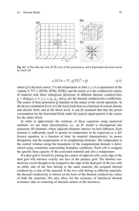
cVoT=ot ¼ r � g rTð ÞT þQ ð4:1Þwhere Q is the heat source, T is the temperature at time t, cV is a capacitance of thevolume V, rT = [∂T/∂x, ∂T/∂y, ∂T/∂z], and the matrix g is the conductivity matrix
of material with three orthogonal directions of different thermal conductivities
g = diag(ga), a = x, y, z, gx, gy, and gz are the thermal conductivities coefficients.
The source of heat generation Q depends on the nature of the circuit operation. At
the device simulation level, it is the local Joule heat as a function of current density
and electric field, and at the block level, it can be assumed that that the power
consumption for the functional block under the typical signal pattern is the source
for the entire block.
In order to approximate the solutions of these equations using numerical
methods, we use finite discretization, i.e., an IC model is decomposed into
numerous 3D elements, where adjacent elements interact via heat diffusion. Each
element is sufficiently small to permit its temperature to be expressed as a dif-
ference equation, as a function of time, its material characteristics, its power
dissipation, and the temperatures of its neighboring elements. The temperature in
the control volumes along the boundaries of the computational domain is deter-
mined using constraints representing boundary conditions. Each cell is assigned
the specific heat capacity of the associated material and also a temperature.
If a dual grid is formed by joining the centers of adjacent cells, each edge of the
dual grid will intersect exactly one face of the primary grid. The thermal con-
ductivity can be thought to be assigned to the edge of the dual grid. If the two cells
on either side of the face belong to the same material, the assigned thermal
conductivity is that of the material. If the two cells belong to different materials,
the thermal conductivity is chosen on the basis of the thermal conductivity values
of both the materials. We also allow for the existence of interfacial thermal
resistance (due to scattering of thermal carriers at the interface).
z
x
y
T
Q
y
(a)(b)
(c)
z
x
Aeff
x1x2
y1
y2
Fig. 4.3 a The chip top view, b 3D view of the grid point a, and c Equivalent electrical circuitfor each cell
4.1 Thermal Model 87
We take up the Galerkin finite element discretization for the thermal conduction
initial boundary value problems. Balancing the order of differentiation by shifting
one derivative from the temperature to the test function η is beneficial: we use
basis functions that are less smooth since we do not require the second derivatives,
and also we are able to satisfy the natural boundary conditions without having to
include them as a separate residual. The integration by parts in the case of a
multidimensional integral is generalized in the divergence theorem. The surface
heat transfer coefficient h is defined as h = 1/(AeffR), where Aeff is the effective area
normal to the direction of heat flow and R is the equivalent thermal resistance. We
assume a Dirichlet boundary condition of the form T = 0 (absolute temperature
equal to ambient temperature) at the radial and the z = max(z) boundaries. Thiscondition is applied by setting the temperature at the center of the boundary cells
along the radial and the z = max(z) boundaries to 0. Note that the boundary
conditions are specific to the package design. Although different packages with
varying heat sink properties would change the boundary conditions, the general
nature of the solution will not change. The boundary condition at z = min(z) isassumed to be of the mixed type gz∂T/∂z − hT = 0, where gz is the thermal
conductivity in the z direction. Physically, this corresponds to heat loss being
proportional to the difference between the absolute temperature and the ambient
temperature. To simplify the problem, we reduce the originally three-dimensional
model to two active coordinates, while still describing the heat conduction through
a three-dimensional domain; the function describing the temperature distribution
depends only on two spatial coordinate variables though. The surface of the three-
dimensional solid consists of the two cross sections, and of the cylindrical sur-
faces, the inner and the outer. The two cylindrical surfaces may be associated with
boundary condition of any type. We simplify calculation by preintegrating in the
thickness direction, dV = ΔzdS and dS = ΔzdC. The volume integrals are then
evaluated over the cross-sectional area Sc, provided h is independent of z; thesurface integrals are computed as integrals over the contour of the cross-section
Cc. Adding the surface (Newton) boundary condition residual, (4.1) is expressed as
ZSc
gcVoT=otDzdS ¼ZSc
rggðrTÞTDzdSþZSc
gQDzdSþZCc
ghðT � TaÞDzdC
ð4:2Þwhere Ta is the known temperature of the surrounding medium. The domain of the
surface is approximated as a collection of triangles. As the triangles are the finite
elements with straight edges we are only approximating any boundaries that are
curved. This error is controlled by length-adaptive error control [21]. Because the
basis on the standard triangle satisfies the Kronecker delta property, the values of
the degrees of freedom Ti(t), i = 1,… Nf, at the i nodes are simply the values of the
interpolated temperature at the nodes, Ti(t) = T(xi, yi, t). We express the system of
ordinary differential equations (ODEs), which results from the introduction of the
Galerkin finite element test function η (the so-called discretization in space) on
(4.2), as
88 4 Temperature Effects in Deep-Submicron CMOS
XNf
i¼1
CjioTi=ot ¼XNf
i¼1
GjiTi þ Pj; j ¼ 1; . . .;Nf ð4:3Þ
where
Cji ¼ZSc
NjcVNiDzdS i; j ¼ 1; . . .;Nf
Gji ¼ZSc
ðrNjÞhjig rNið ÞTDzdS i; j ¼ 1; . . .;Nf
Pj ¼ PQjþ PCj
þ PGjj ¼ 1; . . .;Nf
PQj¼
ZSc
NjQDzdS j ¼ 1; . . .;Nf
ð4:4Þ
Cji, Gji, denote capacity and conductivity matrices, respectively, PQj designates
internal heat generation and N is piecewise linear Galerkin basis function.
Boundary condition in a weighted residual sense is given as
PCj¼
XNi¼Nfþ1
ZSc
NjcVNiDzdS
� �oTi=ot j ¼ 1; . . .;Nf
PGj¼
XNi¼Nfþ1
ZSc
ðrNjÞhjgðNiÞTDzdS� �
Ti j ¼ 1; . . .;Nf
ð4:5Þ
The analogy between heat flow and electrical conduction is invoked here, since
they are described by exactly the same differential equations for a potential dif-
ference. The temperature is represented as voltage, heat flow represented as
electric current, the term on the left hand side in (4.3) represented as a capacitor
and the rest of the terms on the right hand side represented as conductances, giving
rise to an RC circuit [26]. The resulting thermal network in (4.3) is represented in
state space form with the grid cell temperatures as states and the power con-
sumption as inputs to this system
CjiðdTi=dtÞ ¼ GjiTiðtÞ þ BjPjðtÞ ð4:6Þwhere Cji, Gji ∈ Rmji9mji are matrices describing the reactive and dissipative parts
in the model, respectively, Ti(t) ∈ Rmi are time-varying temperature vectors,
Bj ∈ Rmj9pj is the input selection matrix and Pj(t) ∈ Rpj is the vector of power
inputs (heat sources as function of time, wherever they exists). The number of state
variables m is called the order of (4.6), and p is the number of inputs. The outputs
of this state space model are the temperatures at the sensor locations which are
observed by sensor readings Sj(t) ∈ Rqj
SjðtÞ ¼ ETj TiðtÞ ð4:7Þ
4.1 Thermal Model 89
where Ej ∈ Rqj9mj is the output matrix, which identifies the sensor grid cells at
which temperatures are observable. For simplicity, and since this holds true for
electrical circuits, we restrict ourselves to (4.7) with q = p. We are assuming that
distinct measurements are coming from distinct sensors: Ej has only one nonzero
element per row. We connect the nodes of the thermal network of the grid cells
(Fig. 4.3) to the nodes of their neighboring cells through the coupling relations
PjðtÞ ¼ Kj1S1ðtÞ þ � � � þ KjkSkðtÞ þ DjPðtÞ; j ¼ 1; . . .; k
SðtÞ ¼ L1S1ðtÞ þ � � � þ LkSkðtÞð4:8Þ
where Kjk ∈ Rpj9q, Dj ∈ Rpj9p, Lj ∈ Rq9qj are coupling matrixes.
If I – H(s)K is invertible, the input–output relation of the coupled system (4.6),
(4.7) and (4.8) can be written as S(s) = Γ(s)P(s), where S(s) and P(s) are the
Laplace transforms of S(t) and P(t), respectively, and the closed-loop transfer
function Γ(s) has the form
CðsÞ ¼ LðI � HðsÞKÞ�1HðsÞD
HðsÞ ¼ diagðH1ðsÞ; . . .;HkðsÞÞ HjðsÞ ¼ ETj ðsCj � GjÞ�1
Bjð4:9Þ
We express a generalized state space realization of Γ(s) by
CðdT=dtÞ ¼ GTðtÞ þ BPðtÞ C ¼ C 2 Rm;m G ¼ Gþ BKET 2 Rm;m
SðtÞ ¼ ETTðtÞ B ¼ BD 2 Rm;p ET ¼ PET 2 Rq;m ð4:10Þ
Thermal issues arising from the high density of integration in 3D architectures
necessitates the use of aggressive thermal management techniques, and the
inclusion of thermal effects in the architecture space exploration stage of the
design flow. Given the gravity of thermal issues encountered deep within die-
stacks, a runtime power management strategy is essential towards ensuring a
reliable design. A comprehensive thermal management policy for 3D multipro-
cessors incorporating temperature aware workload migration and run-time global
power-thermal budgeting is presented in [27]. Within the policy, processing ele-
ments with available temperature budgets executing high instructions per cycle
workloads are scaled to higher voltage and frequency levels in order to improve
performance after weighing the potential performance benefits of such scaling
against the consequent thermal implications for neighboring processing elements.
We incorporate a runtime power manager with a thermal simulation engine to
yield a methodology for temperature power simulation of 3D architectures [24]. In
the case of MPSoCs, the activity rate is replaced by a cycle-accurate trace of each
processing element execution, indicating the cycles during which computational
operations were performed, and those during which it remained idle. The voltage
and frequency levels of processing elements are controlled by a custom power
management scheme that enables the investigation of the thermal implications of
various power management techniques on 3D stacks. The scheme based on [24]
and extended in [25] uses instantaneous temperature monitoring coupled with
information on the physical structure of the die-stack to determine operating
90 4 Temperature Effects in Deep-Submicron CMOS
voltage-frequency levels for processing elements. Additionally, a weighted policy
is adapted while implementing scaling decisions, thereby preventing processing
elements on deeper tiers from reaching critical temperatures and thus being turned
off. The methodology outperforms conventional 2D dynamic voltage and fre-
quency scaling technique, both in its ability to maintain the temperatures of all
processing elements stable, as well as in its improvement of performance by
increasing the aggregate system frequency [24, 25].
4.2 Temperature Estimation
The thermal behavior of complex deep-submicron VLSI circuits is affected by
various factors, such application dependent localized heating. In addition, process
variations impact the total power consumption (by largely affecting the leakage
component) and, hence, the temperature behavior of each chip, generating dif-
ferent thermal profiles. Power management techniques, such as local clock gating,
further create a disparity in power densities among different regions on a chip.
As a result, complex integrated circuits with large die area require multiple
thermal sensors to capture temperatures at a wide range of locations as the
unpredictability of a workload leads to continuous migration of hot spots, and
within-die manufacturing variations lead to parameter variability that further
conceal the locations of the thermal hot spots. However, the thermal sensors,
together with their support circuitry and wiring, complicate the design process and
increase the total die area and manufacturing costs.
Given the limitations on the number of thermal sensors, it is necessary to
optimally place them near potential hot spot locations. In [28], a clustering
algorithm is described that computes the thermal sensor positions that best serve
clusters of potential hot spot locations. In [29], an optimal sensor problem is
computed as the unite-covering problem. In [30], the unknown temperature at a
particular location is computed as a weighted combination of the known mea-
surements at other locations. Nevertheless, these techniques may be ineffective for
dynamic thermal tracking or if the accuracy or availability of sensors measure-
ments is in question. The size of the grid improves the effectiveness of the sensor
infrastructure in many cases; however, in others, the hotspots may simply be
located such that even a sizable grid of sensors will be incapable of capturing the
locations of significant thermal events. In [31], the maximum distance from
the hotspot within which a sensor can be placed is based on the assumption that the
temperature decays exponentially from a hotspot neglecting the effect of the
location and power consumptions of other power sources on the temperature
around a hotspot. In [32], a systematic technique for thermal sensor allocation and
placement in microprocessors is introduced, which identifies an optimal physical
location for each sensor such that steep thermal gradient is maximized. Never-
theless, this approach does not consider the accuracy of the sensors and does not
guarantee the maximum error in the thermal sensor readings.
4.1 Thermal Model 91

Several online techniques have been proposed to solve the above problem
[14–20]. Among these techniques Kalman filter (KF) based methods generate
thermal estimates for all chip locations while countering sensor noise and can be
applied to real-time thermal tracking problems. The KF propagates the mean and
covariance of the probability density function of the model state in an optimal
(minimum mean square error) way in case of linear dynamic systems. However, as
VLSI fabrication technology continues to scale down, leakage power can take up
to 50 % of the total chip power consumption [33]. Note that leakage has the
nonlinear nature that increase exponentially with the chip temperature. As a
consequence, the standard Kalman filter tends to under-estimate the actual chip
temperature due to the assumed linear model. Consider (4.10) in corresponding
discrete-time state space
Tn ¼ ATn�1 þ JðPDðn�1Þ þ PLðn�1ÞÞ þ rn�1
¼ ATn�1 þ JPDðn�1Þ þ JK1T2n�1e
K2=Tn�1 þ rn�1
¼ f ðTn�1Þ þ rn�1
Sn ¼ hðTnÞ þ un
ð4:11Þ
where Tn is the state vector representing temperatures at different grid cells at time
n, A and J are coefficient matrices determined by the circuit parameters (C and G)and the chosen length of the time step. For clarity, we subdivided power P into two
components, dynamic power PD(n−1) and leakage power PL(n−1). While dynamic
power consumption PD(n−1) = ½αCLVDD2 f, where CL is switching capacitance, α is
switching activity of output node, VDD is supply voltage and f is the operation
frequency of system, is weakly coupled with temperature variation, static power
consumption is a strong function of temperature PLðn�1Þ ¼ K1T2n�1e
K2=Tn�1 [34],
where K1 and K2 are design/technology and fixed supply voltage constants,
respectively. Sn is the output vector of temperatures at sensor locations, rn−1 * N
(0, Rn−1) is the Gaussian process noise, and un * N(0, Un) is the Gaussian sensor
noise (noise caused by fabrication variability, supply voltage fluctuation, cross
coupling etc.).
Due to unpredictability of workloads (power vector is unknown until runtime)
and fabrication/environmental variabilities, the exact value of Tn at runtime is
difficult to predict. To elevate the issue, on-chip sensors provide an observation
vector Sn, which is essentially a subset of Tn plus sensor noise un. In (4.11), h(.) is atransformation function determined by the sensor placement. Due to the sensors
power/area overheads, their number and placement are highly constrained. As a
consequence, the problem of tracking the entire thermal profile (vector Tn) basedon only a few limited sensor observations Sn is rather complex.
To extend the model for the nonlinear leakage-temperature function f(.), themost common way of applying the KF is in the form of the extended Kalman filter
(EKF). In the EKF, the probability density function is propagated through a linear
approximation of the system around the operating point at each time instant. These
approximations, however, can introduce large errors in the true posterior mean and
92 4 Temperature Effects in Deep-Submicron CMOS
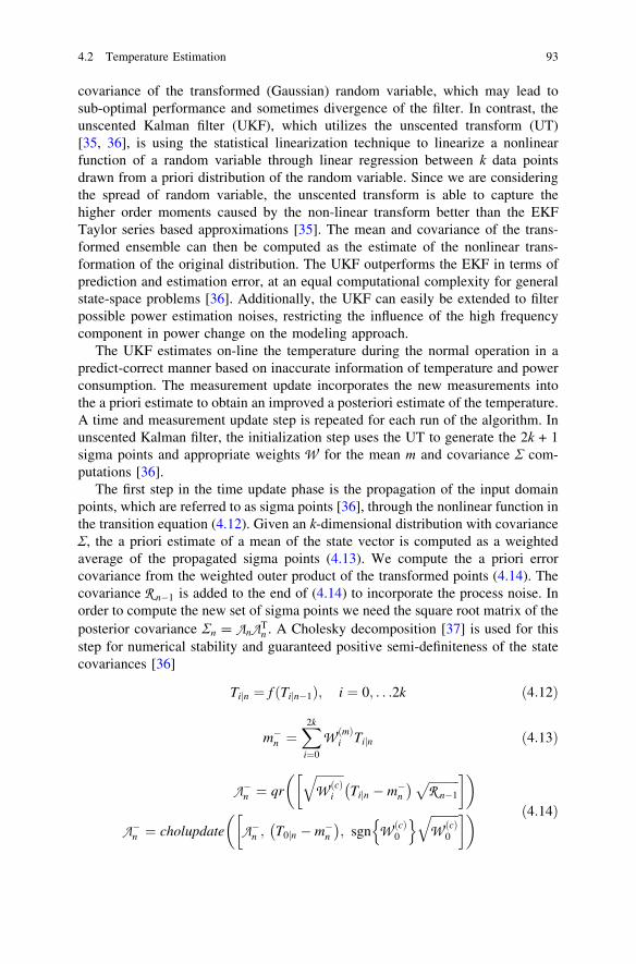
covariance of the transformed (Gaussian) random variable, which may lead to
sub-optimal performance and sometimes divergence of the filter. In contrast, the
unscented Kalman filter (UKF), which utilizes the unscented transform (UT)
[35, 36], is using the statistical linearization technique to linearize a nonlinear
function of a random variable through linear regression between k data points
drawn from a priori distribution of the random variable. Since we are considering
the spread of random variable, the unscented transform is able to capture the
higher order moments caused by the non-linear transform better than the EKF
Taylor series based approximations [35]. The mean and covariance of the trans-
formed ensemble can then be computed as the estimate of the nonlinear trans-
formation of the original distribution. The UKF outperforms the EKF in terms of
prediction and estimation error, at an equal computational complexity for general
state-space problems [36]. Additionally, the UKF can easily be extended to filter
possible power estimation noises, restricting the influence of the high frequency
component in power change on the modeling approach.
The UKF estimates on-line the temperature during the normal operation in a
predict-correct manner based on inaccurate information of temperature and power
consumption. The measurement update incorporates the new measurements into
the a priori estimate to obtain an improved a posteriori estimate of the temperature.
A time and measurement update step is repeated for each run of the algorithm. In
unscented Kalman filter, the initialization step uses the UT to generate the 2k + 1
sigma points and appropriate weights W for the mean m and covariance Σ com-
putations [36].
The first step in the time update phase is the propagation of the input domain
points, which are referred to as sigma points [36], through the nonlinear function in
the transition equation (4.12). Given an k-dimensional distribution with covariance
Σ, the a priori estimate of a mean of the state vector is computed as a weighted
average of the propagated sigma points (4.13). We compute the a priori error
covariance from the weighted outer product of the transformed points (4.14). The
covariance Rn�1 is added to the end of (4.14) to incorporate the process noise. In
order to compute the new set of sigma points we need the square root matrix of the
posterior covariance Σn = ΛnΛTn . A Cholesky decomposition [37] is used for this
step for numerical stability and guaranteed positive semi-definiteness of the state
covariances [36]
Tijn ¼ f ðTijn�1Þ; i ¼ 0; . . .2k ð4:12Þ
m�n ¼
X2ki¼0
WðmÞi Tijn ð4:13Þ
Λ�n ¼ qr
ffiffiffiffiffiffiffiffiffiW
ðcÞi
qTijn � m�
n
� � ffiffiffiffiffiffiffiffiffiffiRn�1
p� �� �
Λ�n ¼ cholupdate Λ�
n ; T0jn � m�n
� �; sgn W
ðcÞ0
n o ffiffiffiffiffiffiffiffiffiW
ðcÞ0
q� �� � ð4:14Þ
4.2 Temperature Estimation 93

where qr function returns only the lower triangular matrix. The weights are not
time dependent and do not need to be recomputed for every time interval. The
superscripts m and c on the weights refer to their use in mean and covariance
calculations, respectively. Note that this method differs substantially from general
sampling methods (e.g., Monte-Carlo methods such as particle filters, which
require orders of magnitude more sample points in an attempt to propagate an
accurate (possibly non-Gaussian) distribution of the state.
The known measurement equation h(.) is used to transform the sigma points
into a vector of respective (predicted) measurements (4.15). The a priori mea-
surement vector is computed as a weighted sum of the generated measurements
(4.16)
Sijn ¼ h Tijn� �
; i ¼ 0; . . .; 2k ð4:15Þ
l�n ¼X2ki¼0
WðmÞi Sijn ð4:16Þ
In the correction step, the computation of the Kalman gain (and, consequently,
the correction phase of the filtering) is based on the covariance of the measurement
vector (4.17) where Un is the measurement noise covariance, and the covariance of
the state and measurement vectors (4.18). These are computed using the weights
(which were obtained from the UT during the initialization step) and the deviations
of the sigma points from their means.
Zn ¼ qr
ffiffiffiffiffiffiffiffiffiffiW
ðmÞi
qSijn � l�n� � ffiffiffiffi
Up
n
� �� �
Zn ¼ cholupdate Zn; S0jn � l�n� �
; sgnfWðmÞ0 g
ffiffiffiffiffiffiffiffiffiffiW
ðmÞ0
q� �� � ð4:17Þ
Nn ¼X2ki¼0
WðcÞi Tijn � m�
n
� �Sijn � l�n� �T ð4:18Þ
The Kalman gain is then computed from these covariance matrices (4.19). We
calculate the a posteriori estimate mn in (4.20) as a combination of the a priori
estimate of a mean of the state vector and a weighted difference between the
measurement result Sn and its a priori prediction. The a posteriori estimate of the
error covariance matrix is updated using (4.21)
Kn ¼ ðNn=ZTn Þ=Zn ð4:19Þ
mn ¼ m�n þ Kn½Sn � l�n � ð4:20Þ
Λn ¼ cholupdateðΛ�n ; KnZn;� 1Þ ð4:21Þ
94 4 Temperature Effects in Deep-Submicron CMOS
where/denotes a back-substitution operation as a superior alternative to the matrix
inversion. Obtained values of mn and Λn become the input of the successive
prediction-correction loop.
4.3 Reducing Computation Complexity
We introduce two techniques that significantly reduce the computational com-
plexity of the thermal model. One of the techniques includes techniques for fast
numerical convergence, while the other provides fast and accurate model order
reduction (MOR) technique of dynamic IC thermal network.
The ODE in (4.3) needs to be numerically integrated in time as analytical
solutions are not possible in general. Although many time marching numerical
methods for solving ODEs are based on methods that do not require explicit
differentiation, these methods are conceptually based on repeated Taylor series
expansions around increasing time instants. Revisiting these roots and basing time
marching on Taylor series expansion allows element-by-element time step adap-
tation by supporting the extrapolation of temperatures at arbitrary times. The
model order reduction enables us to find a low-dimensional but accurate
approximation of the thermal network (4.10), which preserves the input–output
behavior to a desired extent. In this section, we describe a balanced stochastictruncation [38] model order reduction of thermal networks to provide a uniform
approximation of the frequency response of the original system over the whole
frequency domain and to preserve phase information.
4.3.1 Modified Runge–Kutta Solver
We firstly designate numerical dissipation and boundary condition terms and treat
them separately. We adopt a more stable semi-implicit treatment of the numerical
dissipation terms, which is formally correct for the Crank-Nicolson scheme, but
implies a modification of dissipation terms in (4.3) for the Runge–Kutta scheme.
Rewriting the spatially discrete system in (4.3) as
oTot ¼ GðTÞ � CðTÞT ð4:22Þ
where Г(T)T denotes the numerical dissipation term, the predictor–corrector
scheme is
4.2 Temperature Estimation 95
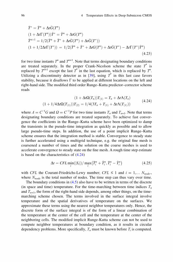
�T� ¼ �Tn þ Dt�GðTnÞð1þ DtCðTnÞÞT� ¼ Tn þ DtGðTnÞ�Tnþ1 ¼ 1=2ð�Tn þ �T� þ Dt�GðTnÞ þ Dt�GðT�ÞÞð1þ 1=2DtCðT�ÞÞ ¼ 1=2ðTn þ T� þ DtGðTnÞ þ Dt�GðT�Þ � DtCðT�ÞTnÞ
ð4:23Þfor two time instants Tn and Tn+1. Note that terms designating boundary conditions
are treated separately. In the proper Crank-Nicolson scheme the state T* is
replaced by Tn+1 except the last T* in the last equation, which is replaced by Tn.Utilizing a discontinuity detector as in [39], using T* in this last case favors
stability, because it disallows Г to be applied at different locations on the left and
right-hand side. The modified third order Runge–Kutta predictor–corrector scheme
reads
ð1þ DtXðTnÞÞTð1Þ ¼ Tn þ DtKðTnÞð1þ 1=4DtXðTð1ÞÞÞTð2Þ ¼ 1=4ð3Tn þ Tð1Þ þ DtKðTð1ÞÞÞ
ð4:24Þ
where Λ = C−1G and Ω = C−1P for two time instants Tn and Tn+1. Note that terms
designating boundary conditions are treated separately. To achieve fast conver-
gence the coefficients in the Runge–Kutta scheme have been optimized to damp
the transients in the pseudo-time integration as quickly as possible and to allow
large pseudo-time steps. In addition, the use of a point implicit Runge–Kutta
scheme ensures that the integration method is stable. Convergence to steady state
is further accelerated using a multigrid technique, e.g. the original fine mesh is
coarsened a number of times and the solution on the coarse meshes is used to
accelerate convergence to steady state on the fine mesh. A rough time step estimate
is based on the characteristics of (4.24)
Dt ¼ CFLmini
jSijð Þ=maxi
�Tni þ Tn
i ;�Tni � Tn
i
� � ð4:25Þ
with CFL the Courant-Friedrichs-Lewy number; CFL ≤ 1 and i = 1,… Nnode.,
where Nnode is the total number of nodes. The time step can thus vary over time.
The boundary conditions in (4.5) also have to be written in terms of the discrete
(in space and time) temperature. For the time-marching between time indices Tnand Tn+1, the form of the right-hand side depends, among other things, on the time-
marching scheme chosen. The terms involved in the surface integral involve
temperature and the spatial derivatives of temperature on the surfaces. We
approximate these terms using the nearest neighbor temperatures only. Hence, the
discrete form of the surface integral is of the form of a linear combination of
the temperature at the center of the cell and the temperature at the center of the
neighboring cells. The modified implicit Runge-Kutta scheme can not be used to
compute neighbor temperatures at boundary condition, as it results in circular
dependency problems. More specifically, Tn must be known before Ti is computed.
96 4 Temperature Effects in Deep-Submicron CMOS
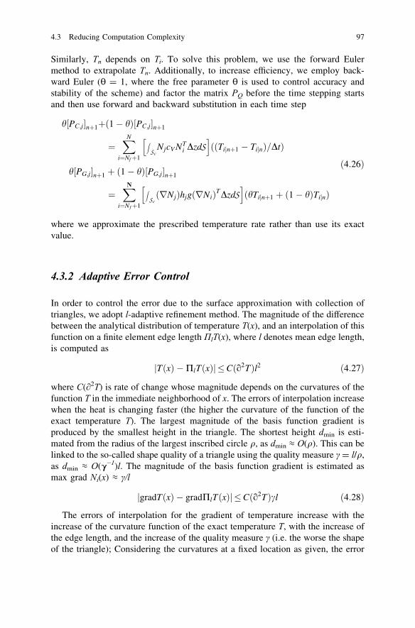
Similarly, Tn depends on Ti. To solve this problem, we use the forward Euler
method to extrapolate Tn. Additionally, to increase efficiency, we employ back-
ward Euler (θ = 1, where the free parameter θ is used to control accuracy and
stability of the scheme) and factor the matrix PQ before the time stepping starts
and then use forward and backward substitution in each time step
h½PC;j�nþ1þð1� hÞ½PC;j�nþ1
¼XN
i¼Nfþ1
ZScNjcVN
Ti DzdS
h iððTijnþ1 � TijnÞ=DtÞ
h½PG;j�nþ1 þ ð1� hÞ½PG;j�nþ1
¼XN
i¼Nfþ1
ZScðrNjÞhjgðrNiÞTDzdS
h iðhTijnþ1 þ ð1� hÞTijnÞ
ð4:26Þ
where we approximate the prescribed temperature rate rather than use its exact
value.
4.3.2 Adaptive Error Control
In order to control the error due to the surface approximation with collection of
triangles, we adopt l-adaptive refinement method. The magnitude of the difference
between the analytical distribution of temperature T(x), and an interpolation of this
function on a finite element edge length ΠlT(x), where l denotes mean edge length,
is computed as
jTðxÞ �PlTðxÞj �Cðo2TÞl2 ð4:27Þwhere C(∂2T) is rate of change whose magnitude depends on the curvatures of the
function T in the immediate neighborhood of x. The errors of interpolation increasewhen the heat is changing faster (the higher the curvature of the function of the
exact temperature T). The largest magnitude of the basis function gradient is
produced by the smallest height in the triangle. The shortest height dmin is esti-
mated from the radius of the largest inscribed circle q, as dmin ≈ O(q). This can be
linked to the so-called shape quality of a triangle using the quality measure γ = l/q,as dmin ≈ O(γ−1)l. The magnitude of the basis function gradient is estimated as
max grad Ni(x) ≈ γ/l
jgradTðxÞ � gradPlTðxÞj �Cðo2TÞcl ð4:28ÞThe errors of interpolation for the gradient of temperature increase with the
increase of the curvature function of the exact temperature T, with the increase of
the edge length, and the increase of the quality measure γ (i.e. the worse the shapeof the triangle); Considering the curvatures at a fixed location as given, the error
4.3 Reducing Computation Complexity 97
will decrease as O(l) as l → 0 (note that this is one order lower than for the
temperatures themselves: by reducing l with a factor of two, the error will decreasewith the same factor). Importantly, from (4.28) we can read that the gradient is
obtained by differentiation of the computed temperature, which immediately
results in a reduction of the order of dependence on the mesh size. For quantity q,the error is then reduced by decreasing the edge length size
EqðlÞ ¼ qex � ql � Clb
liml!0
EqðlÞ ¼ liml!0
Clb ¼ 0 for b[ 0ð4:29Þ
where the exponent of the length size β is the rate of convergence.
4.3.3 Balanced Stochastic Truncation Model OrderReduction
To guarantee the passivity of the reduced model and simplify the computational
procedure, we first convert original descriptor systems into standard state-space
equations by mapping C ! I, G ! C�1G and B ! C�1B. If we define
Φ(s) = Γ(s)ΓT(−s), and let W be a square minimum spectral factor of Φ, satisfying
ðsÞ ¼ WTð�sÞWðsÞ, a state space realization ðGW; BW; EWÞ of WðsÞ can be
obtained as
GW ¼ G BW ¼ Bþ YE ETW ¼ ET � BT
WX ð4:30Þwhere Y is the controllability Gramian (e.g. the low rank approximation to the
solution) of Γ given by Lyapunov equation
GY þ YGT þ BBT ¼ 0 ð4:31Þand X is the observability Gramian of W, being solution of the Riccati equation
XG þ GTX þ EFET þ XBWM�1BT
WX ¼ 0 ð4:32Þwhere F 2 Rp�p is symmetric, positive semi-definite and M 2 Rm�m is symmetric,
positive definite. In the iterative procedure we approximate the low rank Cholesky
factors Ξ and Θ, such that ΘTΘ ≈ X and ΞTΞ ≈ Y. We obtain the observability
Gramian X by solving the Riccati equation (4.32) with a Newton double step
iteration
GT � Zðz�1ÞBTW
�XðzÞ þ XðkÞ G � BWZ
ðz�1ÞT �
¼ �ETFE� Zðz�1ÞMFZðz�1ÞT
ZðzÞ ¼ XðzÞBWM�1 ð4:33Þ
where the feedback matrix Z ¼ XBWM�1, for z = 1,2,3,…, which generates a
sequence of iterates X(z). This sequence converges towards the stabilizing solution
98 4 Temperature Effects in Deep-Submicron CMOS

X if the initial feedback Z0 is stabilizing, i.e., G-BZ(0)T is stable. If we partition Ψ
and Ψ−1 as Ψ = [J U] and Ψ−1=[O V]−1 then Il = OJ is the identity matrix,
Π = JO is a projection matrix, and O and J are truncation matrices. In the related
balancing model reduction methods, the truncation matrices O and J can be
determined knowing only the Cholesky factors of the Gramians Y and X. If we letΞTΘ = UΣVT, where Σ = diag(σ1,…,σl), be singular value decomposition (SVD)
of ΞTΘ, then we can calculate the truncation matrices O = Σ−½VTΘ and
J = ΞTUΣ−½. Under a similarity transformation of the state-space model, both
parts can be treated simultaneously after a transformation of the system
ðC_; G_; B_; E_T
Þ with a nonsingular matrix Ψ∈ Rm�m into a stochastically balanced
system
C_ ¼ JTCO G
_ ¼ JTGO B_ ¼ JTB E
_ ¼ EO ð4:34Þ
where C_
; G_ 2 Rl�l, B
_ 2 Rl�p and E_ 2 Rp�l are of order l much smaller than the
original order m, if controllability Gramian Y satisfies W�1YW�T ¼ WTXW. Note
that SVDs are arranged so that the diagonal matrix containing the singular values
has the same dimensions as the factorized matrix and the singular values appear in
non-increasing order.
4.4 System Level Methodology for TemperatureConstrained Power Management
The progression towards smaller technology nodes has enabled an increase in
integration density of modern silicon dies. The reduction in feature sizes has also
exposed issues such as process variation, leakage power consumption, and the
limitations of interconnect performance [40]. 3D integration is an emerging
solution that targets these challenges through die-stacking and the use of through
silicon via (TSV) based vertical interconnects. In the context of multiprocessor
systems on-chip (MP-SoC), die stacking improves system scalability by allowing
the integration of a larger number of processing elements (PE), without the
associated increase in the chip’s overall area footprint. The increased integration
density, however, exposes multiple design challenges on account of the incorpo-
ration of logic, memory and the TSV-based vertical interconnect within the same
die-stack [41, 42]. The design of the vertical interconnect, for instance, is com-
plicated by the keep out zone requirement, which serves to insulate circuit ele-
ments from the mechanical stress induced by the thermal expansion and
contraction of through silicon vias. The choice of keep out zone also determines
the area, the electrical noise and the delay characteristics of the vertical inter-
connect. It is essential that these parameters and their effects be taken into account
during early 3D architecture space exploration in order to yield a vertical
4.3 Reducing Computation Complexity 99
interconnect design that achieves the desired electrical performance, within the
available silicon area.
State of the art high-performance MP-SoCs contain a large number of general
and special purpose processing elements that significantly increase power density
when integrated within a single diestack. As a consequence, thermal issues are
observed especially in the lower tiers of the die-stack [43–45]. The vertical
interconnect structure reduces the magnitude of these issues to some extent as it
improves the number of heat transfer paths in the stack [46], and thus the thermal
conductance to the higher tiers.
During conventional architecture space exploration, processing elements and
memory blocks are placed based on simulation results at locations that yield the
best system performance. However, such a technology-oblivious approach may
aggravate thermal issues and inadvertently reduce system performance in 3D
stacked designs. Hence, initial system floorplans must be evaluated in terms of
their thermal performance alongside conventional system performance during 3D
architecture space exploration. While thermal performance analysis provides
critical feedback on the floorplan of the system, variations in the behavior of
different target applications may necessitate multiple iterations of the analysis.
Even so, an optimal solution satisfying all applications may remain elusive. In
such cases a runtime power management scheme provides the degree of adapt-
ability required to maintain thermal performance even with dynamic application
behavior. In this section these design challenges are addressed through a system-
level methodology that enables architecture space exploration based on the per-
formance and cost of vertical interconnect structures, and the thermal behavior of
die-stacks. Furthermore, it presents a runtime power management scheme to
maintain thermal performance of such stacks despite variations in workload
behavior.
4.4.1 Overview of the Methodology
A number of studies have investigated the challenges of stacked-die architectures,
and have attempted to address the need for an analysis and exploration method-
ology for 3D designs. Exploration tool in [47], which enables automated floor-
planning, routing, placement of through silicon vias and the thermal profiling of
stacked-die architectures, illustrate the performance benefits of stacked-die
architectures and their associated thermal issues. However, the method does not
include the planning of the 3D through silicon via network, nor are the keep out
zone considerations taken into account in their placement. Moreover, while the
method includes support for thermal via insertion, it does not support the use of a
runtime power manager alongside the performance simulation. Although thermal
vias can reduce the severity of thermal issues at tiers far from the heatsink, a
runtime power management strategy can suitably manage the temperature profile
of the stack thereby reducing the number of such vias required. Inclusion of the
100 4 Temperature Effects in Deep-Submicron CMOS
power management strategy during analysis of thermal performance is therefore
critical towards preventing the insertion of vias where they are not necessary. In
[48] a thermal-aware floorplanner for 3D stacked processor cores is presented that
considers the power dissipation of the interconnect during floorplan exploration.
Despite its merits, this methodology too does not describe keep out zone con-
siderations, nor the placement of through silicon vias within the floorplan.
Moreover, it does not include support for a runtime power manager in its analysis.
An example of how such exploration tools benefit application performance in
multiprocessor systems can be found in [49], where the optimal topology for an
application specific 3D multiprocessor is investigated, in terms of placement
options for processing elements and memory blocks. Through an exploratory
simulation, multiple topologies are evaluated in terms of their average data access
cost, and whether the consequent temperature of logic blocks remains within the
imposed design constraints. Based on the findings, an optimal topology is devised
for the 3D multiprocessor.
A system-level methodology in [25] incorporates both vertical interconnect
exploration and thermal performance analysis in a single flow along with a runtime
power management scheme to enable 3D architecture space exploration. Vertical
interconnects may contain through silicon vias arranged in several topologies. For
instance, they may be organized as bundles, or be placed along the boundaries of
the vertical interconnect area. Each topology exhibits a different electrical per-
formance and a distinct area penalty.
Thus, the first step in the flow consists of a method to explore through silicon
vias placement topologies for multi-tier die-stacks. Topologies are analyzed on the
basis of their electrical performance and area penalty using parameterized through
silicon via models according to the system specifications and the initial floorplan
[50]. The results from this exploration allow the initial floorplan to be revised in
order to incorporate the through silicon via topology found superior in terms of
electrical performance and cost, and better achieve target specifications. The
revised floorplan may differ from the initial in several ways, especially in the
number of TSVs that constitute the vertical link on each tier of the die-stack. Since
the through silicon vias essentially act as vertical heat transfer paths within the
diestack, a significantly different thermal conductance can be expected when
compared to the initial floorplan. These characteristics of the vertical interconnect
are taken into account in the thermal modeling stage in which a mesh of thermal
cells is generated for each device tier in order to determine its thermal relationship
with others in the stack. The resulting thermal model provides a comprehensive set
of effective thermal relationships between blocks in the 3D floorplan. The final
stage of the flow is a temperature-power simulation that incorporates a thermal
simulator using the model from the previous step, as well as a power estimation
function that computes the power dissipation of logic blocks derived from the
initial system specifications and their activity rate. Based on this, the temperature-
power simulator determines the effective thermal profile for the 3D stack [24]. In
the case of MPSoCs, the activity rate is replaced by a cycle-accurate trace of each
processing element execution, indicating the cycles during which computational
4.4 System Level Methodology 101
operations were performed, and those during which it remained idle. The voltage
and frequency levels of processing elements are controlled by a custom power
management scheme that enables the investigation of the thermal implications of
various power management techniques on 3D stacks. Based on the analysis of a
conventional dynamic voltage-frequency scaling (DVFS) technique, a novel
temperature-constrained power management scheme is presented that controls the
voltage and frequency levels of processing elements based on their temperature
and physical position in the stack, as well as the thermal model of the die-stack.
4.4.2 Temperature-Power Simulation
Thermal issues arising from the high density of integration in 3D architectures
necessitates the use of aggressive thermal management techniques, and the
inclusion of thermal effects in the architecture space exploration stage of the
design flow. Recent studies [49] illustrate the performance benefits of defining 3D
multiprocessor systems on-chip architecture based on thermal simulation results.
However, given the gravity of thermal issues encountered deep within die-stacks, a
runtime power management strategy is essential towards ensuring a reliable
design. It is also prudent for such runtime schemes to be included within the
simulation setup in order to better understand the thermal performance of 3D
architectures.
Dynamic voltage and frequency scaling (DVFS) is a commonly used runtime
power management technique that operates processing elements at different
voltage and frequency levels according to their workload [51]. Improvements in
application performance as well as the effective utilization of power budget are
reported in [52] using a temperature constrained dynamic voltage and frequency
scaling based power management scheme for planar chip multiprocessors (CMP).
The scheme controls the voltage and frequency levels of individual processing
elements based on their local operating temperature, and the available chip power
budget. However, it cannot be applied to 3D architectures since it does not con-
sider thermal coupling between adjacent processing elements—a significant factor
in die stacks [27]. The inefficacy of conventional dynamic voltage and frequency
scaling approaches applied to 3D architectures is highlighted in [53] by analyzing
the variation in thermal conditions between the extremities of deep stacks, that
resulted in processing elements on lower tiers turning off more often than others.
However, a thermal management policy employed requires the use of an inter-tier
liquid cooling system.
In a comprehensive thermal management policy for 3D CMPs [27] incorpo-
rating temperature aware workload migration and run-time global power-thermal
budgeting, processing elements with available temperature budgets executing high
instructions per cycle (IPC) workloads are scaled to higher voltage and frequency
levels in order to improve performance after weighing the potential performance
benefits of such scaling against the consequent thermal implications for
102 4 Temperature Effects in Deep-Submicron CMOS
neighboring processing elements. The flow in system-level methodology [25]
integrates a runtime power manager with a thermal simulation engine to yield a
methodology for temperature power simulation of 3D architectures. This enables
the exploration and refinement of 3D floorplans, and their evaluation in presence
of a runtime power management strategy. A key contribution that resulted from
this methodology is a temperature-constrained power management scheme for 3D
MP-SoCs that uses instantaneous temperature monitoring coupled with informa-
tion on the physical structure of the die-stack to determine operating voltage-
frequency levels for processing elements. The scheme uses a weighted policy
while implementing scaling decisions, thereby preventing processing elements on
deeper tiers from reaching critical temperatures and being turned off. The scheme
outperforms conventional 2D DVFS both in its ability to maintain the temperatures
of all processing elements stable, as well as in its improvement of performance by
increasing the aggregate system frequency.
The temperature-constrained power management scheme for 3D MP-SoCs is
implemented within the customizable power management block (PMB), which is
responsible for controlling the voltage and frequency of processing elements
within the temperature-power simulation. The PMB reads the utilization or activity
rate of each processing element and its temperature, and the total chip power
computed through a power measurement circuit within the power supply, in order
to set new voltage and frequency levels for processing elements at regular inter-
vals. For such a scheme to be effective, it is important to model the dynamics of
the controlled system, i.e. establish the relationship between the manipulated and
the controlled variables. In this case, the operating voltage-frequency level is used
as a manipulated variable to control power and temperature of the system. The
range of dynamic voltage and frequency scaling in MP-SoCs is usually limited,
and within this small range, [54] and [55] observe that the relationship between
power and DVFS level can be approximated with a linear function. The value of
constant, which governs a linear function (representative of activity factor in
dynamic power consumption), depends on the characteristics of the workload
being executed on the processing element, and in cases where the target workload
is known, this may be set to a generalized value. While the thermal conductance
between two processing elements is calculated using conductance equations, due
the complex nature of heat flow, additional information such as the possible heat
transfer paths, as well as the impedance along each such path are necessary in
order to establish a direct relation between the temperature and voltage-frequency
levels. The temperature of a processing element in a 3D stack is primarily
determined by its power dissipation, physical location within the die-stack, and its
area. The power management scheme considers these parameters in determining
appropriate voltage-frequency levels to keep the total chip power below a set
power budget value, while keeping the temperature of processing elements under
critical temperature values. A temperature margin is considered in order to
maintain the temperature of processing elements at a safe distance from the critical
limit even under unexpected circumstances such as noise in the power supply
or a sudden increase in their workload. The system is initialized at maximum
4.4 System Level Methodology 103
voltage-frequency levels, and begins execution with the maximum power dissi-
pation. At the beginning of a new control period, the difference between the total
chip power and the local power budget value is computed. In the event that a new
temperature check cycle has started, the difference between the actual and the
critical temperatures of each processing element is updated.
A less active processing element bearing a strong thermal relation with the
processing element that is close to its critical temperature is considered to have the
heaviest weight, and is thus the prime candidate for voltage-frequency scale down.
If required, the next candidate processing element is selected and scaled down, and
this process continues until the processing element temperature is brought under
the critical value. In the event that the processing element temperature remains at
or exceeds this critical temperature, it is clock gated. Repeated fluctuations
between voltage-frequency levels may, however, be observed in certain cases,
incurring large performance and power penalties. To avoid this, the voltage-fre-
quency levels of processing elements that were scaled down due to a the pro-
cessing element that is close to its critical temperature are prevented from being
reinstated until these processing element is within the safe temperature margin.
The voltage-frequency level of processing elements is pulled up or down based on
their weighted allocated power budget. The weights serve to establish the impact
of these parameters on the choice of processing element for scaling. Since the
height of the stack and area of processing elements may be expected to remain
constant even through floorplan revisions, only the utilization and temperature
margin are considered to be variable. In addition, since the value of utilization may
be generalized for a homogeneous MP-SoC, an exploratory simulation is only
required once to determine the value of the weight, which corresponds to the
temperature margin. Such weighted allocated power budget may be applied to both
island-based as well as per-core schemes. The per-core scheme may simply be
considered as an island scheme in which each island contains only one processing
element. The weight of an island is thus the average weight of all processing
elements within it. For a highly active PE that is cooler, is situated close to the
heatsink and has a larger area, it is the preferred choice for voltage-frequency
upscaling. However, this is performed only if the projected temperature after
scaling is found to be below the safety margin. The processing element with the
largest weight is chosen for voltage-frequency upscaling. This upscaling is per-
formed iteratively until no more processing elements can be pulled up or if the
total power reaches allocated budget value. In the event that the budget has been
exceeded, the pull down stage is invoked in order to achieve convergence. For
voltage-frequency downscaling, the processing element with the smallest weight is
selected and the pull down is performed iteratively until no more processing
elements can be pulled down or until the total power falls below the budget value.
At each instance of pull up and pull down, the difference between the processing
element’s actual and critical temperatures is updated. It is recommended that the
range of voltage-frequency values supported by the algorithm be set keeping in
104 4 Temperature Effects in Deep-Submicron CMOS
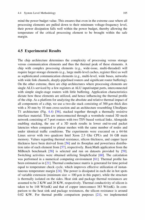
mind the power budget value. This ensures that even in the extreme case where all
processing elements are pulled down to their minimum voltage-frequency level,
their power dissipation falls well within the power budget, thereby allowing the
temperature of the critical processing element to be brought within the safe
margin.
4.5 Experimental Results
The chip architecture determines the complexity of processing versus storage
versus communication elements and thus the thermal peak of these elements. A
chip with complex processing elements (e.g., wide-issue, multi-threaded) will
require larger storage elements (e.g., large multi-level caches, register files) as well
as sophisticated communication elements (e.g., multi-level, wide buses, networks
with wide link channels, deeply-pipelined routers and significant router buffering).
On the other extreme, there are chip architectures where processing elements are
single ALUs serviced by a few registers at ALU input/output ports, interconnected
with simple single-stage routers with little buffering. Application characteristics
dictate how these elements are utilized, and hence influencing the thermal profile
of the chip. As a platform for analyzing the absolute and relative thermal impact of
all components of a chip, we use a two-die stack consisting of 300 μm thick dies
with a 30 mm by 10 mm cross-section and an architecture resembling UltraSparc
T1 architecture (Fig. 4.4) [56], stacked together through a thermally resistive
interface material. Tiles are interconnected through a wormhole routed 3D mesh
network consisting of 7-port routers with two TSV-based vertical links. Alongside
enabling stacking, the use of a 3D mesh results in lower end-to-end packet
latencies when compared to planar meshes with the same number of nodes and
under identical traffic conditions. The experiments were executed on a 64-bit
Linux server with two quadcore Intel Xeon 2.5 Ghz CPUs and 16 GB main
memory. Values regarding thermal resistance, silicon thickness, and copper layer
thickness have been derived from [56] and its floorplan and power/area distribu-
tion ratio of each element from [57], respectively. BasicMath application from the
MiBench benchmark [58] is selected and run on datasets provided by [59].
Switching activities were obtained utilizing SimpleScalar [60]. The calculation
was performed in a numerical computing environment [61]. Thermal profile has
been estimated as in [21]. Thermal conductance matrix is generated for time period
equal to temperature check cycle, which improves effective utilization of instan-
taneous temperature margin [24]. The power is dissipated in each die in hot spots
of variable extension (minimum size = 100 μm in this paper), while the structure
is thermally isolated on the sides. Heat sink and package thermal resistances are
assumed to be 2 K/W and 20 K/W, respectively. Thermal conductivity of silicon is
taken to be 148 W/(mK) and that of copper interconnect 383 W/(mK). In com-
parison to the heat sink and package resistances, the silicon resistance is around
0.02 K/W. For thermal profile comparison purposes [21], we implemented
4.4 System Level Methodology 105
generalized finite element method, which can be found in several commercially
available software packages (e.g. Hotspot [62], Ansys [63]). The accuracy of a
discretization concerns the rate of convergence as function of mesh size. The
truncation error consists of the discretization applied to the exact solution.
Figure 4.5a) illustrates that the numerical accuracy of the Galerkin method with
l-adaptive error control is 1–2 order of magnitude more accurate for comparable
mesh size than corresponding generalized finite element method. Furthermore, we
compared modified Runge-Kutta solver with Euler (as in Hotspot [62]) and
Newmark (in Ansys [63]).
The method offers increased accuracy, while simultaneously increases solution
efficiency, and theoretically, can reach accuracy of O(Δt4). On the other hand, the
accuracy of Euler method is O(Δt2). The errors in Euler scheme are dominated by
the deterministic terms as long as the step-size is large enough. In more detail, the
error of the method behaves like O(α2 + εα + ε2α1/2), when ε is used to measure
the smallness of the temperature and a is the time-step. The smallness of the
temperature also allows special estimates of the local error terms, which can be
used to control the step-size. An efficient implementation of the Newmark methods
for linear problems requires that direct methods (e.g. Gauss elimination) be used
for the solution of the system of algebraic equations. When a step size should be
updated, the prediction of the new step size has to be made such that the prescribed
accuracy can be achieved with the least cost. The rate of convergence of the global
error in the Newmark integration can be O(Δt2). Correspondingly, the rate of
convergence of the local error should achieve O(Δt3). Suppose that the current
time-step is α, then we have O(κα3), where κ is a constant depending on the exact
solution. By utilizing the balanced stochastic truncation MOR technique for
Fig. 4.4 UltraSparc T1
architecture chip micrograph
(Copyright Sun
Microsystems)
106 4 Temperature Effects in Deep-Submicron CMOS
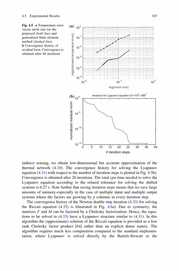
indirect sensing, we obtain low-dimensional but accurate approximation of the
thermal network (4.10). The convergence history for solving the Lyapunov
equation (4.31) with respect to the number of iteration steps is plotted in Fig. 4.5b).
Convergence is obtained after 26 iterations. The total cpu-time needed to solve the
Lyapunov equation according to the related tolerance for solving the shifted
systems is 0.27 s. Note further that saving iteration steps means that we save large
amounts of memory-especially in the case of multiple input and multiple output
systems where the factors are growing by p columns in every iteration step.
The convergence history of the Newton double step iteration (4.33) for solving
the Riccati equation (4.32) is illustrated in Fig. 4.6a). Due to symmetry, the
matrices F and M can be factored by a Cholesky factorization. Hence, the equa-
tions to be solved in (4.33) have a Lyapunov structure similar to (4.31). In this
algorithm the (approximate) solution of the Riccati equation is provided as a low
rank Cholesky factor product [64] rather than an explicit dense matrix. The
algorithm requires much less computation compared to the standard implemen-
tation, where Lyapunov is solved directly by the Bartels-Stewart or the
0 5 10 15 20 25 30 35 4010
-15
-2
-3
-4
10
10
-210
10
10
10
-1
10 -1
10-10
10-5
-5
100
100
100
norm
aliz
ed r
esid
ual n
orm
# iteration steps
iterations for Lyapunov equation GY+YGT=-BBT
(a)
(b)
Fig. 4.5 a Temperature error
versus mesh size for the
proposed (bold line) andgeneralized finite element
method (dashed line),b Convergence history of
residual form. Convergence is
obtained after 46 iterations
4.5 Experimental Results 107
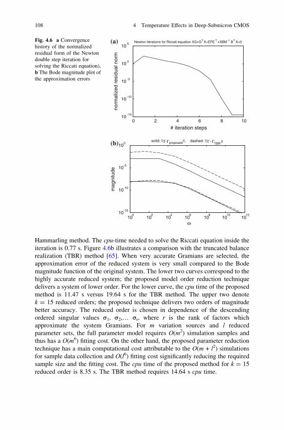
Hammarling method. The cpu-time needed to solve the Riccati equation inside the
iteration is 0.77 s. Figure 4.6b illustrates a comparison with the truncated balance
realization (TBR) method [65]. When very accurate Gramians are selected, the
approximation error of the reduced system is very small compared to the Bode
magnitude function of the original system. The lower two curves correspond to the
highly accurate reduced system; the proposed model order reduction technique
delivers a system of lower order. For the lower curve, the cpu time of the proposed
method is 11.47 s versus 19.64 s for the TBR method. The upper two denote
k = 15 reduced orders; the proposed technique delivers two orders of magnitude
better accuracy. The reduced order is chosen in dependence of the descending
ordered singular values σ1, σ2,… σr, where r is the rank of factors which
approximate the system Gramians. For m variation sources and l reduced
parameter sets, the full parameter model requires O(m2) simulation samples and
thus has a O(m6) fitting cost. On the other hand, the proposed parameter reduction
technique has a main computational cost attributable to the O(m + l2) simulations
for sample data collection and O(l6) fitting cost significantly reducing the required
sample size and the fitting cost. The cpu time of the proposed method for k = 15
reduced order is 8.35 s. The TBR method requires 14.64 s cpu time.
0 2 4 6 8 1010
-15
10-10
10-5
100
105
norm
aliz
ed r
esid
ual n
orm
# iteration steps
Newton iterations for Riccati equation XG+GT X=EFE T +XBM -1 BT X=0
100
102
104
106
108
1010
101210
-15
10-10
10-5
100
ω
mag
nitu
de
solid: ||Γ-Γproposed||, dashed: ||Γ -ΓTBR ||
(a)
(b)
Fig. 4.6 a Convergence
history of the normalized
residual form of the Newton
double step iteration for
solving the Riccati equation),
b The Bode magnitude plot of
the approximation errors
108 4 Temperature Effects in Deep-Submicron CMOS
In the experiments, the temperature values of the grid cell containing the
sensors are observable, while the temperature at other grid cells are estimated with
proposed unscented Kalman filter. We assumed 16 9 16 chip gridding granularity.
Furthermore, for thermal tracking, we assumed that sensors are uniformly scat-
tered on the chip. The number of samples and the sample locations is varied. No
specific sensor technology is assumed in this chapter. The readings from the
temperature sensors initiate the estimation algorithm. The transformation matrix h(.) in (4.11) is determined by the sensor placement. Gaussian noise is superim-
posed on the actual temperature values to model the inaccuracies of real thermal
sensors, such as supply voltage fluctuation, fabrication variability, cross coupling,
etc. Processes generating these noises are assumed to be stationary between dif-
ferent successive prediction-correction steps. Actual temperatures at the sensor
locations and locations of interest are obtained with the proposed Galerkin method
and acquired results compared with HotSpot [62] and Ansys [63] as in Fig. 4.5a).
In this sense, the measurement error designates the temperature difference between
sensors readings and real temperature at locations of interest in the observed grid
cell. We compare the accuracy of our approach to that of the Kalman filter [17]
and extended Kalman filter [19]. In Kalman filter (KF) dynamic model function f(.)in (4.11) is linear Gaussian model. Such a model does not account for the non-
linear temperature-circuit parameters dependency and, as consequence, its
usability in the practical applications is restricted. Furthermore, due to the inac-
curacy of its linear model, the standard Kalman filter relies excessively on the
accuracy of sensor input. The temperature estimates derived from the Kalman filter
are non-anticipative in the sense that they are only conditional to sensor mea-
surements obtained before and at the time step n. However, after we have obtainedmeasurements, we could compute temperature estimates of Tn−1, Tn−2, …, which
are also conditional to the measurements after the corresponding state time steps.
With the Rauch-Tung-Striebel smoother, more measurements and more informa-
tion are available for the estimator. Consequently, these temperature estimates are
more accurate than the non-anticipative measurements computed by the KF. The
EKF approximate the nonlinearities with linear or quadratic functions or explicitly
approximate the filtering distributions by Gaussian distributions. In UKF, the
unscented transform is used for approximating the evolution of Gaussian distri-
bution in non-linear transforms. Figure 4.7a illustrate that the proposed method
always keep track of the actual temperature with high accuracy for a randomly
chosen chip location that does not coincide with the sensor location. For clarity,
we only depicted UKF tracking. There is no observable difference between the
reduced model results and the original model results, which suggests high accu-
racy of model order reduction. Based on (4.11), we simulated the thermal profile of
the test processor for a total duration of 600 s (the simulation starts at room
temperature). This is assumed to be the real chip temperature and is used to
measure estimation accuracy. We examine the mean absolute error and the stan-
dard deviation of the error as the location of interest. These values are averaged
over all the locations of interest. High precision of temperature tracking is obtained
(within 0.5 °C for mean and 1.1 °C for standard deviation) for various cases,
4.5 Experimental Results 109
ranging from two to six sensors, respectively, placed at an arbitrary location
around the hotspot. In integrated circuits, the placement of the sensors is con-
strained to areas where there is enough spatial slack due to the limitations such as
additional channels for routing and input/output. For thermal sensors, if one sensor
per router is not affordable for large on-chip networks, the network can be parti-
tioned into regions and multiple adjacent routers within a region could share the
same sensor. The proposed technique is able to estimate the temperature at the
locations far away from the limited number of sensors. As anticipated, the Kalman
techniques are relatively independent of the relative position of the sensor and the
location of interest. The UKF obtain almost identical accuracy (variations of less
than 0.3 °C) across the examined range significantly outperforming KF and EKF,
especially when the number of sensors is small. This difference is highlighted in
Fig. 4.7b. Note that 1 °C accuracy translates to 2 W power savings [66]. The state
vector representing temperatures at different grid cells at time n in (4.11) and
function f(.) is determined by the circuit parameters and the chosen length of time
steps. Statistics of measurement and estimation errors for different sizes of time
steps is evaluated too. The chosen time step is at 10−4 s and multiplied by powers
of two. Thermal profiles transition in 3D ICs is a very slow process and a
noticeable temperature variation takes at least several hundred milliseconds to
change; accordingly, a few millisecond overhead for reading noisy thermal sensors
will not impact the effectiveness of dynamic thermal management unit. High
precision within 1.1 °C for both, mean and standard deviation is obtained even
with a large time step size. The average error (across all chip locations) of each
method is reported as we vary the sensor noise level as defined in (4.11).
As we increase the noise level, the estimation accuracy generated by KF and
EKF degrades more rapidly in contrast to UKF, which generate accurate thermal
estimates (within 0.8 °C) under all examined circumstances. The improved per-
formance of the UKF compared to the EKF is due to two factors, namely, the
increased time-update accuracy and the improved covariance accuracy. In the
UKF case, the covariance estimation is very accurate, which results in a different
Kalman gains in the measurement-calibration equation and hence the efficiency of
the measurement-calibration step. The advantage of EKF over UKF is its relative
simplicity compared to its performance. Nevertheless, since EKF is based on a
local linear approximation, its accuracy is limited in highly nonlinear systems.
Also the filtering model is restricted in the sense that only Gaussian noise pro-
cesses are allowed and thus the model cannot contain, for example, discrete valued
random variables. The Gaussian restriction also prevents handling of hierarchical
models or other models where significantly non-Gaussian distribution models
would be needed. The EKF also formally requires the measurement model and
dynamic model functions to be differentiable. Even when the Jacobian matrices
exist and could be computed, the actual computation and programming of Jacobian
matrices is error prone and hard to debug. On the other hand, UKF is not based on
local linear approximation; UKF utilizes a bit further points in approximating the
non-linearity. The computational load increases when moving from the EKF to the
UKF if the Jacobians are computed analytically (the average runtime of EKF
110 4 Temperature Effects in Deep-Submicron CMOS
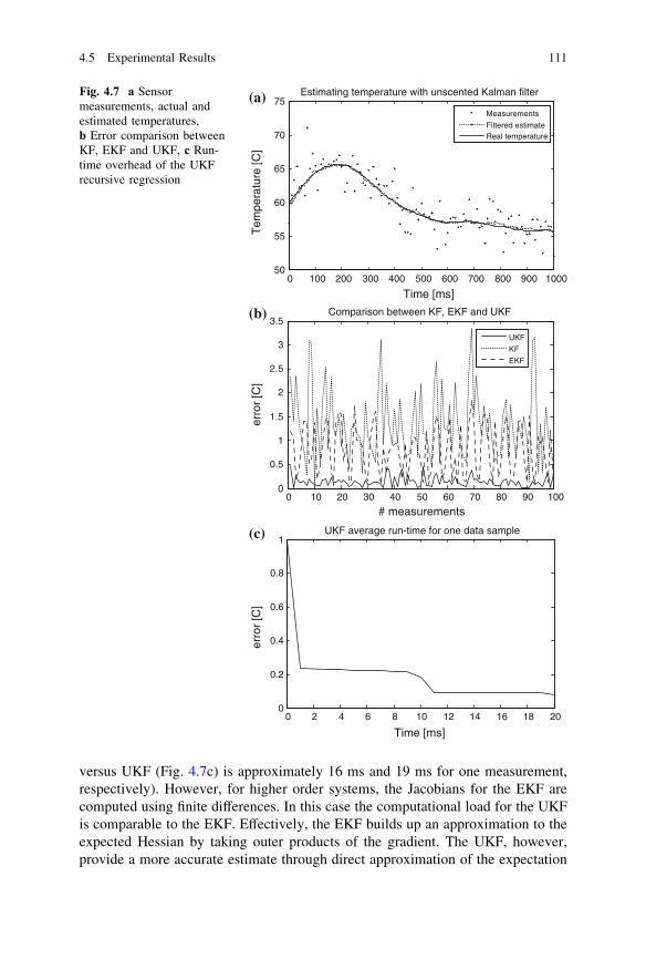
versus UKF (Fig. 4.7c) is approximately 16 ms and 19 ms for one measurement,
respectively). However, for higher order systems, the Jacobians for the EKF are
computed using finite differences. In this case the computational load for the UKF
is comparable to the EKF. Effectively, the EKF builds up an approximation to the
expected Hessian by taking outer products of the gradient. The UKF, however,
provide a more accurate estimate through direct approximation of the expectation
0 100 200 300 400 500 600 700 800 900 100050
55
60
65
70
75Estimating temperature with unscented Kalman filter
Time [ms]
Tem
pera
ture
[C]
Measurements
Filtered estimateReal temperature
0 10 20 30 40 50 60 70 80 90 1000
0.5
1
1.5
2
2.5
3
3.5
# measurements
erro
r [C
]
Comparison between KF, EKF and UKF
UKF
KF
EKF
0 2 4 6 8 10 12 14 16 18 200
0.2
0.4
0.6
0.8
1
erro
r [C
]
Time [ms]
UKF average run-time for one data sample
(a)
(b)
(c)
Fig. 4.7 a Sensor
measurements, actual and
estimated temperatures,
b Error comparison between
KF, EKF and UKF, c Run-
time overhead of the UKF
recursive regression
4.5 Experimental Results 111
of the Hessian. Note that another distinct advantage of the UKF occurs when either
the architecture or error metric is such that differentiation with respect to the
parameters is not easily derived as necessary in the EKF. The UKF effectively
evaluates both the Jacobian and Hessian precisely through its sigma point prop-
agation, without the need to perform any analytic differentiation
4.6 Conclusions
Due to the temperature sensors power/area overheads and the limitations such as
additional channels for routing and input/output, their number and placement are
highly constrained to areas where there is enough spatial slack. As a consequence,
the problem of tracking the entire thermal profile based on only a few limited
sensor observations is rather complex. This problem is further aggravated due to
unpredictability of workloads and fabrication/environmental variabilities. Within
this framework, to improve thermal management efficiency we present method-
ology based on unscented Kalman filter for accurate temperature estimation at all
chip locations while simultaneously countering sensor noise. As the results indi-
cate, the described method generates accurate thermal estimates (within 1.1 °C)under all examined circumstances. In comparison with KF and EKF, the UKF
consistently achieves a better level of accuracy at limited costs. Additionally, to
provide significant reductions on the required simulation samples for constructing
accurate models we introduce a balanced stochastic truncation MOR. The
approach produces orthogonal basis sets for the dominant singular subspace of the
controllability and observability Gramians, exploits low rank matrices and avoids
large scale matrix factorizations, significantly reducing the complexity and com-
putational costs of Lyapunov and Riccati equations, while preserving model order
reduction accuracy and the quality of the approximations of the TBR procedure.
References
1. W. Topol et al., Three-dimensional integrated circuits. IBM J. Res. Dev. 50(4/5), 491–506(2006)
2. C. Ababei, Y. Feng, B. Goplen, H. Mogal, T.P. Zhang, K. Bazargan, S. Sapatnekar,
Placement and routing in 3D integrated circuits. IEEE Des. Test Comput. 22(6), 520–531(2005)
3. S. Im, K. Banerjee, “Full chip thermal analysis of planar (2-D) and vertically integrated (3-D)
high performance ICs, in Proceedings of IEEE International Electron Devices Meeting,pp. 727–730, (2000)
4. J. Torresola et al., Density factor approach to representing impact of die power maps on
thermal management. IEEE Trans. Adv. Packag. 28(4), 659–664 (2005)
5. J. Cong, J. Wei, Y. Zhang, A thermal-driven floorplanning algorithm for 3D ICs”, in
Proceedings of IEEE International Conference on Computer-Aided Design, pp. 306–313(2004)
112 4 Temperature Effects in Deep-Submicron CMOS
6. T.-Y. Chiang, S.J. Souri, C.O. Choi, K.C. Saraswat, Thermal analysis of heterogeneous 3-D
ICs with various integration schemes, in Proceedings of IEEE International Electron DevicesMeeting, pp. 681–684 (2001)
7. T.T. Wang, Y.M. Lee, C.C.P. Chen, 3D thermal ADI—an efficient chip-level transient
thermal simulator. IEEE Trans. Comput. Aided Des. Integr. Circuits Syst. 21(12), 1434–1445(2002)
8. K.J. Scott, Electrostatic potential Green’s functions for multi-layered dielectric media.
Philips J. Res. 45, 293–324 (1990)
9. A. Vincenzi, A. Sridhar, M. Ruggiero, D. Atienze, Fast thermal simulation of 2D/3D
integrated circuits exploiting neural networks and GPUs, in Proceedings of IEEEInternational Symposium on Low Power Electronic Design, pp. 151–156 (2011)
10. A.M. Niknejad, R. Gharpurey, R.G. Meyer, Numerically stable Green function for modeling
and analysis of substrate coupling in integrated circuits. IEEE Trans. Comput. Aided Des.
Integr. Circuits Syst. 17(4), 305–315 (1998)
11. B. Wang, P. Mazumder, Fast thermal analysis for VLSI circuits via semi-analytical Green’s
function in multi-layer materials, in Proceedings of IEEE International Symposium onCircuits and Systems, vol. 2, pp. 409–412 (2004)
12. N. Allec, Z. Hassan, L. Shang, R.P. Dick, R. Yang, ThermalScope: Multi-scale thermal
analysis for nanometer-scale integrated circuits, in Proceedings of IEEE InternationalConference on Computer-Aided Design, pp. 603–610 (2008)
13. A.M. Ionescu, G. Reimbold, F. Mondon, Current trends in the electrical characterization of
low-k dielectrics, in Proceedings of IEEE International Semiconductor Conference, pp. 27–36(1999)
14. Y. Zhang, A. Srivastava, M. Zahran, Chip level thermal profile estimation using on-chip
temperature sensors, in Proceedings of IEEE International Conference on Computer Design,pp. 432–437 (2008)
15. R. Cochran, S. Reda, Spectral techniques for high resolution thermal characterization with
limited sensor data, in Proceedings of IEEE Design Automation Conference, pp. 478–483(2009)
16. S. Sharifi, C.-C. Liu, T. Simunic Rosing, Accurate temperature estimation for efficient
thermal management, in Proceedings of IEEE International Symposium on Quality ElectronicDesign, pp. 137–142 (2008)
17. Y. Zhang, A. Srivastava, M. Zahran, Chip level thermal profile estimation using on-chip
temperature sensors, in Proceedings of IEEE International Conference on Computer Design,pp. 1065–1068 (2008)
18. H. Jung, M. Pedram, A stochastic local hot spot alerting technique, in Proceedings of theIEEE Asia and South Pacific Design Automation Conference, pp. 468–473 (2008)
19. S. Sharifi, T.S. Rosing, Accurate direct and indirect on-chip temperature sensing for efficient
dynamic thermal management. IEEE Trans. Comput. Aided Des. Integr. Circuits Syst. 29(10), 1586–1599 (2010)
20. Y. Zhang, A. Srivastava, Adaptive and autonomous thermal tracking for high performance
computing systems, in Proceedings of IEEE Design Automation Conference, pp. 68–73
(2010)
21. A. Zjajo, N. van der Meijs, R. van Leuken, Thermal analysis of 3D integrated circuits based
on discontinuous Galerkin finite element method, in Proceedings of IEEE InternationalSymposium on Quality Electronic Design, pp. 117–122 (2012)
22. W. Huang, S. Ghosh, S. Velusamy, K. Sankaranarayanan, K. Skadron, M.R. Stan, Hotspot: a
compact thermal modeling methodology for early-stage VLSI design. IEEE Trans. VLSI
Syst. 14(5), 501–513 (2006)
23. Y. Xie, Processor architecture design using 3D integration technology, in Proceedings ofIEEE International Conference on VLSI Design, pp. 446–451 (2010)
24. A. Aggarwal, S.S. Kumar, A. Zjajo, R. van Leuken, Temperature constrained power
management scheme for 3D MPSoC, in IEEE International Workshop on Signal and PowerIntegrity, pp. 7–10 (2012)
References 113
25. S.S. Kumar, A. Aggarwal, R. Jagtap, A. Zjajo, R. van Leuken, A system level methodology
for interconnect aware and temperature constrained power management of 3D MP-SOCs, in
IEEE Transactions on VLSI Systems, (in press)
26. J. Lienhard, A heat transfer textbook (Phlogiston Press, Cambridge, 2006)
27. C. Zhu et al., Three-dimensional chip-multiprocessor run-time thermal management. IEEE
Trans. Comput. Aided Des. Integr. Circuits Syst. 27(8), 1479–1492 (2008)
28. S.O. Memik, R. Mukherjee, M. Ni, J. Long, Optimizing thermal sensor allocation for
microprocessors. IEEE Trans. Comput. Aided Des. Integr. Circuits Syst. 27(3), 516–527(2008)
29. B.-H. Lee, T. Kim, Optimal allocation and placement of thermal sensors for reconfigurable
systems and its practical extension, in Proceedings of IEEE Asia and South Pacific DesignAutomation Conference, pp. 703–707 (2008)
30. F. Liu, A general framework for spatial correlation modeling in VLSI design, in Proceedingsof IEEE Design Automation Conference, pp. 817–822 (2007)
31. R. Mukherjee, S.O. Memik, Systematic temperature sensor allocation and placement for
microprocessors, in Proceedings of IEEE Design Automation Conference, pp. 542–547 (2006)32. K.-J. Lee, K. Skadron, Analytical model for sensor placement on microprocessors, in
Proceedings of IEEE International Conference on Computer Design, pp. 24–27 (2005)
33. N. Kim et al., Leakage current: Moore’s law meets static power. IEEE Comput. 36(12),68–75 (2003)
34. L. He, W. Liao, M. Stan, System level leakage reduction considering the interdependence of
temperature and leakage, in Proceedings of IEEE Design Automation Conference, pp. 12–17(2004)
35. S.J. Julier, J.K. Uhlmann, Unscented filtering and nonlinear estimation. Proc. IEEE 92(3),401–422 (2004)
36. R. van der Merwe, E.A. Wan, The square-root unscented Kalman filter for state and
parameter-estimation, in Proceedings of IEEE International Conference on Acoustics, Speechand Signal Processing, pp. 3461–3464 (2001)
37. G.H. Golub, C.F. van Loan, Matrix Computations. (Johns Hopkins University Press, 1996)
38. M. Green, Balanced stochastic realizations. Linear Algebra Appl. 98, 211–247 (1988)
39. L. Krivodonova, Limiters for high-order discontinuous Galerkin methods. J. Comput. Phys.
226, 879–896 (2007)
40. J. Kim et al., High-frequency scalable electrical model and analysis of a through silicon via
(tsv). IEEE Trans. Compon. Packag. Manuf. Technol. 1(2), 181–195 (2011)
41. T. Kgil et al., Picoserver: Using 3D stacking technology to enable a compact energy efficient
chip multiprocessor, in Proceedings of International conference on Architectural Support forProgramming Languages and Operating Systems, pp. 117–128 (2006)
42. G. Loh, 3D-stacked memory architectures for multi-core processors, in Proceedings ofInternational Symposium on Computer Architecture, pp. 453–464 (2008)
43. A. Sridhar et al., 3D-ICE: Fast compact transient thermal modeling for 3D ICs with inter-tier
liquid cooling, in Proceedings of International Conference on Computer-Aided Design,pp. 463–470 (2010)
44. A. Jain, et al., Thermal modeling and design of 3D integrated circuits, in Proceedings of theIntersociety Conference on Thermal and Thermomechanical Phenomena in ElectronicSystems, pp. 1139–1145 (2008)
45. C. Sun, L. Shang, R.P. Dick, Three-dimensional multiprocessor system-on-chip thermal
optimization, in Proceedings of International Hardware/Software Codesign and SystemSynthesis Conference, pp. 117–122 (2007)
46. J. Cong, J.Wei, Y. Zhang, A thermal-driven floorplanning algorithm for 3D ICs, in
Proceedings of International Conference on Computer-Aided Design, pp. 306–313 (2004)
47. J. Cong, A. Jagannathan, Y. Ma, G. Reinman, J. Wei, Y. Zhang, An automated design flow
for 3D microarchitecture evaluation, in Proceedings of the Asia and South Pacific DesignAutomation Conference, pp. 384–389 (2006)
114 4 Temperature Effects in Deep-Submicron CMOS
48. W.-L. Hung, et al., Interconnect and thermal-aware floorplanning for 3D microprocessors, in
Proceedings of the International Symposium on Quality Electronic Design, pp. 98–104 (2006)
49. O. Ozturk, F. Wang, M. Kandemir, Y. Xie, Optimal topology exploration for application-
specific 3D architectures, in Proceedings of the Asia and South Pacific Design AutomationConference, pp. 390–395 (2006)
50. R. Jagtap, S.S. Kumar, R. van Leuken, A methodology for early exploration of tsv placement
topologies in 3D stacked ics, in Proceedings of Euromicro Conference on Digital SystemDesign, pp. 382–388 (2012)
51. S. Herbert, D. Marculescu, Analysis of dynamic voltage/frequency scaling in chip-
multiprocessors, in Proceedings of International Symposium on Low Power Electronics andDesign, pp. 38–43 (2007)
52. X. Wang, K. Ma, Y. Wang, Adaptive power control with online model estimation for chip
multiprocessors. IEEE Trans. Parallel Distrib. Syst. 22(10), 1681–1696 (2011)
53. M.M. Sabryz, D. Atienza, A.K. Coskuny, Thermal analysis and active cooling management
for 3D MPSoCs, in Proceedings of International Symposium on Circuits and Systems,pp. 2237–2240 (2011)
54. R. Raghavendra, et al., No “power” struggles: coordinated multilevel power management for
the data center, in Proceedings of the International Conference on Architectural support forprogramming languages and operating systems, pp. 48–59 (2008)
55. X. Wang, M. Chen, Cluster-level feedback power control for performance optimization, in
Proceedings of International Symposium on High Performance Computer Architecture,pp. 101–110 (2008)
56. A. Leon, K. Tam, J. Shin, D. Weisner, F. Schumacher, A power efficient high-throughput 32-
thread SPARC processor, in Proceedings of IEEE International Solid-State CircuitsConference, pp. 295–304 (2006)
57. A.K. Coskun, T.S. Rosing, K. Whisnant, Temperature aware task scheduling in MPSoCs, in
Proceedings of IEEE Design, Automation and Test in Eurupe Conference, pp. 1–6 (2007)
58. MiBench http://www.eecs.umich.edu/mibench/
59. G. Fursin, J. Cavazos, M. O’Boyle, O. Temam, MiDataSets: Creating the conditions for a
more realistic evaluation of iterative optimization, in Proceedings of International Conferenceon High-Performance and Embedded Architectures and Compilers, pp. 245–260 (2007)
60. SimpleScalar http://www.simplescalar.com/
61. MatLab http://www.mathworks.com/
62. K. Skadron, K. Sankaranarayanan, S. Velusamy, D. Tarjan, M.R. Stan, W. Huang,
Temperature-aware micro-architecture: modeling and implementation. ACM Trans.
Architect. Code Optim. 1(1), 94–125 (2004)
63. Ansys 10.0 http://www.ansys.com
64. T. Reis, T. Stykel, PABTEC: Passivity-preserving balanced truncation for electrical circuits.
IEEE Trans. Comput. Aided Des. Integr. Circuits Syst. 29(9), 1354–1367 (2010)
65. J. Li, J. White, Efficient model reduction of interconnect via approximate system Grammians,
in Proceedings of IEEE International Conference on Computer Aided Design, pp. 380–384(1999)
66. E. Rotem, J. Hermerding, C. Aviad, C. Harel, Temperature Measurement in the Intel Core
Duo Processor, in Proceedings of IEEE International Workshop on Thermal Investigations ofICs, pp. 23–27 (2006)
References 115
Chapter 5Circuit Solutions
CMOS technologies move steadily towards finer geometries, which provide higherdigital capacity, lower dynamic power consumption and smaller area resulting inintegration of whole systems, or large parts of systems, on the same chip. However,due to technology scaling, integrated circuits are becoming more susceptible tovariations in process parameters and noise effects like power supply noise, cross-talkreduced supply voltage and threshold voltage operation severely impacting theyield [1]. Since parameter variations depend on unforeseen operational conditions,chips may fail despite they pass standard test procedures. Similarly, the magnitude ofthermal gradients and associated thermo-mechanical stress increase further asCMOS designs move into nanometer processes and multi-GHz frequencies [1].Higher temperature increases the risk of damaging the devices and interconnectssince major back-end and front-end reliability issues including electro-migration,time-dependent dielectric breakdown, and negative-bias temperature instabilityhave strong dependence on temperature. As a consequence, continuous observationof process variation and thermal monitoring becomes necessity. Such observation isenhanced with dedicated monitors embedded within the functional cores [2]. In orderto maximize the coverage, the process variation and thermal sensing devices arescattered across the entire chip to meet the control requirements. The monitors arenetworked by an underlying infrastructure, which provides the bias currents to thesensing devices, collects measurements, and performs analog to digital signal con-version. Therefore, the supporting infrastructure is an on-chip element at a globalscale, growing in complexity with each emerging design.
The process variation and temperature monitors for signal integrity measure-ment systems of VLSI circuits should meet several requirements including com-patibility with the target process with no additional fabrication steps, highaccuracy, a small silicon area and low power consumption. In a ring-oscillatorbased technique [3], isolation of individual parameters for variability study ischallenging due to mixture of the variation of large number of transistors into asingle parameter (i.e. the frequency of ring operation). On the other hand, thetransistor array based structures [4] enable collection of transistor I–V curves withdigital I/O, enabling measurement of I–V characteristics of a larger number ofdevices than is typically sustained by common dc probing measurement schemes.
A. Zjajo, Stochastic Process Variation in Deep-Submicron CMOS, Springer Seriesin Advanced Microelectronics 48, DOI: 10.1007/978-94-007-7781-1_5,� Springer Science+Business Media Dordrecht 2014
117

Such structures use row and column decoders to select an individual transistor inthe transistor array and employ different schemes to address the IR drop imposedby the transmission gates on a transistor’s selection path. Temperature monitorbased on time-to-digital-converter [5] is constrained by the large area and poweroverhead at the required sampling rate. Temperature monitor operating in the sub-threshold region [6] is prone to dynamic variations as thermal sensitivity increasesby an order of magnitude when operating in sub-threshold [7]. Consequently, themajority of CMOS temperature monitors are based on the temperature charac-teristics of parasitic bipolar transistors [8].
In this chapter, we present compact, low area, low power process variation andtemperature monitors with high accuracy and wide temperature range that does notneed to operate with special requirements on technology, design, layout, testing oroperation. The monitors operate at the local power supply and are designed tomaximize the sensitivity of the circuit to the target parameter to be measured. Themonitors are small, stand alone and easily scalable, and can be fully switched off.All the peripheral circuits, such as decoders and latches, are implemented withthick gate oxide and long channel devices and are, hence, less sensitive to theprocess variation. To characterize current process variability conditions and enabletest guidance based on the data obtained from the monitors, we utilize theexpectation-maximization algorithm [9] and the adjusted support vector machineclassifier [10], respectively.
This chapter is organized as follows: Sect. 5.1 focuses on the observationstrategy and the overall overview of the system. Section 5.2 discusses design ofprocess variation and temperature monitors. In Sect. 5.3 the algorithms for char-acterization of process variability condition, verification process and test-limitguidance and update are described. In Sect. 5.4, the process variation and tem-perature monitors and algorithms are evaluated on an application example. Finally,Sect. 5.5 provides a summary and the main conclusions.
5.1 Architecture of the System
From a circuit design perspective parametric process variations can be divided intointer-die and intra-die variations. Inter-die variations such as the process tem-perature, equipments properties, wafer polishing, wafer placement, etc. affect alltransistors in a given circuit equally. For the purposes of circuit design, it is usuallyassumed that each component or contribution in inter-die variation is due to dif-ferent physical and independent sources; therefore, the variation component can berepresented by a deviation in the parameter mean of the circuit. Intra-die variationsare deviations occurring within a die. These variations may have a variety ofsources that depend on the physics of the manufacturing steps (optical proximityeffect, dopant fluctuation, line edge roughness, etc.) and the effect of these non-idealities (noise, mismatch) may limit the minimal signal that can be processedand the accuracy of the circuit behavior. For linear systems, the non-linearities of
118 5 Circuit Solutions

the devices generate distortion components of the signals limiting the maximalsignal that can be processed correctly. Although, certain circuit techniques such asusing small modulation index for the bias current to reduce the effect of distortionnon-idealities, large device sizes to lower mismatch and utilizing low-impedancelevel to limit the thermal noise signals, these measures have, however, importantconsequences on the power consumption and operation speed of the system.
In general, the design margins for mixed signal designs depend significantly onprocess parameters and their distributions across the wafer, within a wafer lot andbetween wafer lots, which is especially relevant for mismatch. Measurement of thesefluctuations is paramount for stable control of transistor properties and statisticalmonitoring and the evaluation of these effects enables the efficient development ofthe test patterns and test and debugging methods, as well as ensures good yields. ICmanufacturing facilities try to realize constant quality by applying various methodsto analyze and control their process. Some of the quality control tools include, e.g.histograms, check sheets, pareto charts, cause and effect diagrams, defect concen-tration diagrams, scatter diagrams, control charts, time series models and statisticalquality control tools, e.g. process capability indices, and time series. Process controlmonitoring (PCM) data (electrical parameters, e.g. MOS transistor threshold voltage,gate width, capacitor Q-value, contact chain resistance, thin-film resistor properties,etc. measured from all the test dice on each wafer) is required to utilize these qualitycontrol tools. Making decisions about if the product or process is acceptable, is by nomeans an easy task, e.g. if the process/product is in control and acceptable, or incontrol but unacceptable, or out of control but acceptable. When uncertain, addi-tional tests for the process and/or the product may be required for making thedecision. Masks for wafers are generally designed so that a wafer after being fullyprocessed through the IC manufacturing process will contain several test dice. Thearea consumed by a test die is usually quite large, i.e. sometimes comparable toseveral ordinary production dice. Measuring the electrical properties from the testdice gives an estimate of the quality of the lot processing, and device requirement tofulfill a priori specifications e.g. temperature range, speed. Finally the IC devices aretested for functionality at the block level in the wafer probing stage, and the yield ofeach wafer is appended to the data. The tester creates suitable test patterns andconnects signal generators online. It digitizes the measurement signals and finallydetermines, according to the test limits, if the device performs acceptably or not.Then, the wafer is diced, and the working dice are assembled into packages. Thecomponents are then re-tested, usually in elevated temperature to make sure they arewithin specification.
Silicon wafers produced in a semiconductor fabrication facility routinely gothrough electrical and optical measurements to determine how well the electricalparameters fit within the allowed limits. The yield is determined by the outcome ofthe wafer probing (electrical testing), carried out before dicing. The simplest form ofyield information is the aggregate pass/fail statistics of the device, where the yield isusually expressed as a percentage of good dice per all dice on the wafer. Yield losscan be caused by several factors, e.g. wafer defects and contamination, IC manu-facturing process defects and contamination, process variations, packaging
5.1 Architecture of the System 119
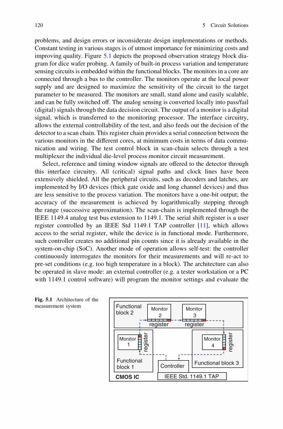
problems, and design errors or inconsiderate design implementations or methods.Constant testing in various stages is of utmost importance for minimizing costs andimproving quality. Figure 5.1 depicts the proposed observation strategy block dia-gram for dice wafer probing. A family of built-in process variation and temperaturesensing circuits is embedded within the functional blocks. The monitors in a core areconnected through a bus to the controller. The monitors operate at the local powersupply and are designed to maximize the sensitivity of the circuit to the targetparameter to be measured. The monitors are small, stand alone and easily scalable,and can be fully switched off. The analog sensing is converted locally into pass/fail(digital) signals through the data decision circuit. The output of a monitor is a digitalsignal, which is transferred to the monitoring processor. The interface circuitry,allows the external controllability of the test, and also feeds out the decision of thedetector to a scan chain. This register chain provides a serial connection between thevarious monitors in the different cores, at minimum costs in terms of data commu-nication and wiring. The test control block in scan-chain selects through a testmultiplexer the individual die-level process monitor circuit measurement.
Select, reference and timing window signals are offered to the detector throughthis interface circuitry. All (critical) signal paths and clock lines have beenextensively shielded. All the peripheral circuits, such as decoders and latches, areimplemented by I/O devices (thick gate oxide and long channel devices) and thusare less sensitive to the process variation. The monitors have a one-bit output; theaccuracy of the measurement is achieved by logarithmically stepping throughthe range (successive approximation). The scan-chain is implemented through theIEEE 1149.4 analog test bus extension to 1149.1. The serial shift register is a userregister controlled by an IEEE Std 1149.1 TAP controller [11], which allowsaccess to the serial register, while the device is in functional mode. Furthermore,such controller creates no additional pin counts since it is already available in thesystem-on-chip (SoC). Another mode of operation allows self-test: the controllercontinuously interrogates the monitors for their measurements and will re-act topre-set conditions (e.g. too high temperature in a block). The architecture can alsobe operated in slave mode: an external controller (e.g. a tester workstation or a PCwith 1149.1 control software) will program the monitor settings and evaluate the
CMOS IC IEEE Std. 1149.1 TAP
Functionalblock 1
Functionalblock 2
Functional block 3Controller
registerregister
regi
ster
regi
sterMonitor
1Monitor
4
Monitor2
Monitor3
Fig. 5.1 Architecture of themeasurement system
120 5 Circuit Solutions
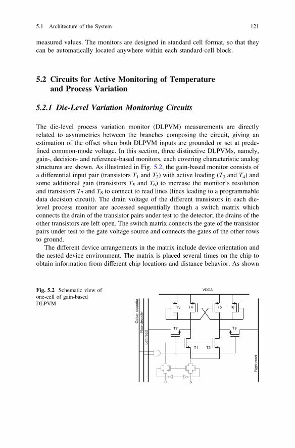
measured values. The monitors are designed in standard cell format, so that theycan be automatically located anywhere within each standard-cell block.
5.2 Circuits for Active Monitoring of Temperatureand Process Variation
5.2.1 Die-Level Variation Monitoring Circuits
The die-level process variation monitor (DLPVM) measurements are directlyrelated to asymmetries between the branches composing the circuit, giving anestimation of the offset when both DLPVM inputs are grounded or set at prede-fined common-mode voltage. In this section, three distinctive DLPVMs, namely,gain-, decision- and reference-based monitors, each covering characteristic analogstructures are shown. As illustrated in Fig. 5.2, the gain-based monitor consists ofa differential input pair (transistors T1 and T2) with active loading (T3 and T4) andsome additional gain (transistors T5 and T6) to increase the monitor’s resolutionand transistors T7 and T8 to connect to read lines (lines leading to a programmabledata decision circuit). The drain voltage of the different transistors in each die-level process monitor are accessed sequentially though a switch matrix whichconnects the drain of the transistor pairs under test to the detector; the drains of theother transistors are left open. The switch matrix connects the gate of the transistorpairs under test to the gate voltage source and connects the gates of the other rowsto ground.
The different device arrangements in the matrix include device orientation andthe nested device environment. The matrix is placed several times on the chip toobtain information from different chip locations and distance behavior. As shown
SG
Col
um d
ecod
erR
ow d
ecod
erLe
ft re
ad
Rig
ht r
ead
VDDA
T7 T8
T1 T2
T3 T4 T5 T6
Fig. 5.2 Schematic view ofone-cell of gain-basedDLPVM
5.1 Architecture of the System 121
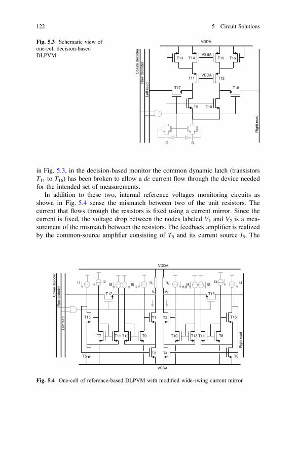
in Fig. 5.3, in the decision-based monitor the common dynamic latch (transistorsT11 to T16) has been broken to allow a dc current flow through the device neededfor the intended set of measurements.
In addition to these two, internal reference voltages monitoring circuits asshown in Fig. 5.4 sense the mismatch between two of the unit resistors. Thecurrent that flows through the resistors is fixed using a current mirror. Since thecurrent is fixed, the voltage drop between the nodes labeled V1 and V2 is a mea-surement of the mismatch between the resistors. The feedback amplifier is realizedby the common-source amplifier consisting of T5 and its current source I5. The
SG
Col
um d
ecod
erR
ow d
ecod
erLe
ft re
ad
Rig
ht r
ead
VDDA
T9 T10
VDDA
VSSA
T11 T12
T13 T14 T15 T16
T17 T18
Fig. 5.3 Schematic view ofone-cell decision-basedDLPVM
T1 T2
Rig
ht r
ead
V2
VSSA
VDDA
Col
um d
ecod
erR
ow d
ecod
erLe
ft re
ad
R1 R2
V1
T3 T4T5 T6
T7 T8T9 T10T11 T12 T13 T14
T15 T16
T17 T18
I1 I2 I3 I4I5 I6I7 I10
I8 I9
Fig. 5.4 One-cell of reference-based DLPVM with modified wide-swing current mirror
122 5 Circuit Solutions
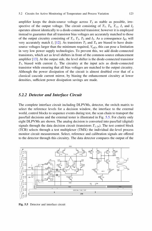
amplifier keeps the drain-source voltage across T3 as stable as possible, irre-spective of the output voltage. The circuit consisting of T7, T9, T11, I1 and I2
operates almost identically to a diode-connected transistor; however it is employedinstead to guarantee that all transistor bias voltages are accurately matched to thoseof the output circuitry consisting of T1, T3, T5 and I5. As a consequence IR1 willvery accurately match I1 [12]. As transistors T3 and T9 are biased to have drain-source voltages larger than the minimum required, Veff3, this can pose a limitationin very low power supply technologies. To prevent this, we add diode-connectedtransistors, which act as level shifters in front of the common-source enhancementamplifier [13]. At the output side, the level shifter is the diode-connected transistorT7, biased with current I2. The circuitry at the input acts as diode-connectedtransistor while ensuring that all bias voltages are matched to the output circuitry.Although the power dissipation of the circuit is almost doubled over that of aclassical cascode current mirror, by biasing the enhancement circuitry at lowerdensities, sufficient power dissipation savings are made.
5.2.2 Detector and Interface Circuit
The complete interface circuit including DLPVMs, detector, the switch matrix toselect the reference levels for a decision window, the interface to the externalworld, control blocks to sequence events during test, the scan chain to transport thepass/fail decisions and the external tester is illustrated in Fig. 5.5. For clarity onlyeight DLPVMs are shown. The analog decision is converted into pass/fail (digital)signals through the data decision circuit (transistors T1-24). The test control block(TCB) selects through a test multiplexer (TMX) the individual die-level processmonitor circuit measurement. Select, reference and calibration signals are offeredto the detector through this circuitry. The data detector compares the output of the
IEEE Std. 1149.1 TAP
ATE
TCBTMX
VSS
outp
VDD
clkT9
T15
QA
QANQ
QAN
QA
clk clk
outp T17 outnT18
T16
T19 T20
T21 T22 T23 T24
clk
2/0.1
nbias
refn
inn
refp
outn
T5
clkT8
T14T12
T7
T10 T11
T6C1
C2
T1
T2
T3
T4
clk
clkn
inp
T13
DLPVM
φ
DLPVM
DLPVM
DLPVM
φ
φn
φn
DLPVM
DLPVM
DLPVM
DLPVM
Q
QN
QN
refs
el
Fig. 5.5 Detector and interface circuit
5.2 Circuits for Active Monitoring of Temperature and Process Variation 123

die level process monitor against a comparison reference window. The referencevoltages defining the decision windows are related to the performance figuresunder study. The robustness against process variations is provided by an auto-zeroing scheme [14]. The data decision circuit operates on a two phase non-overlapping clock. The comparison references needed to define the monitordecision windows are controlled through the dc signals labeled refp and refn. Thedifferencing network samples reference voltage during phase clk onto capacitor C,while the input is shorted giving differential zero. During phase clkn, the inputsignal is applied at the inputs of both capacitors, causing an input differentialvoltage to appear at the input of the comparator preamp. At the end of clkn theregenerative flip-flop is latched to make the comparison and produce digital levelsat the output. In the test mode, two main phases can be distinguished according tothe state of signal /. If / is high, the inputs of the detector are shorted to theanalog ground to perform a test of the detector itself, e.g. the circuit is in the auto-zeroing mode, whereas if / is low the particular die-level process monitor circuitis connected to the detector and tested. The key requirement which determines thepower dissipation during the comparison process in the data detector is theaccuracy, i.e. how accurately the comparator can make a decision in a given timeperiod.
As typical cross-coupled latch comparator exhibit large offset voltage, pre-amplifier is placed before the regenerative latch to amplify the signal for accuratecomparison. The power dissipation in the regenerative latch is relatively smallcompared to the preamp power, as only dynamic power is dissipated in theregenerative latch and low offset pre-amp stages usually require dc bias currents. Ifhigh gain is required from a single stage preamp, the large value of the loadresistor must be used, which in turn slows down the amplification process with anincreased RC-constant at the output. In situations like this, the gain is distributedamong several cascaded low gain stages to speed up the process. During thisprocess care must be also taken to design a low noise pre-amp stage since its owncircuit noise is amplified through its gain. For instance, if the input signal is heldconstant close to the comparator threshold, the thermal noise from both circuitsand input sampling switches is also amplified through the preamp gain. Also, 1/fnoise must be considered since it appears like a slowly varying offset of thecomparator for high speed operation. Periodic offset cancellation at a rate muchhigher than the 1/f noise corner frequency, usually every clock period, can reducethis effect.
Another major factor which affects the accuracy of the comparator is the offsetvoltage caused by the mismatches from process variations. This includes chargeinjection mismatches from input switches, threshold and transistor-dimensionsmismatches between cross-coupled devices. To lessen the impact of mismatch,several schemes, such as inserting a preamplifier [15] in front of the latch, adding achopper amplifier [14] and auto-zero scheme to sample an offset in the capacitor infront of the latch or digital background calibration [16] have been developed. Inthe auto-zero scheme, during the offset sampling period, the output of the firststage caused by its offset voltage is sampled on the sampling capacitor of the
124 5 Circuit Solutions
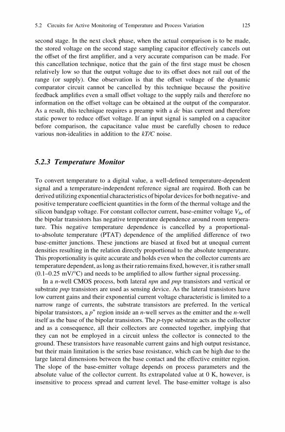
second stage. In the next clock phase, when the actual comparison is to be made,the stored voltage on the second stage sampling capacitor effectively cancels outthe offset of the first amplifier, and a very accurate comparison can be made. Forthis cancellation technique, notice that the gain of the first stage must be chosenrelatively low so that the output voltage due to its offset does not rail out of therange (or supply). One observation is that the offset voltage of the dynamiccomparator circuit cannot be cancelled by this technique because the positivefeedback amplifies even a small offset voltage to the supply rails and therefore noinformation on the offset voltage can be obtained at the output of the comparator.As a result, this technique requires a preamp with a dc bias current and thereforestatic power to reduce offset voltage. If an input signal is sampled on a capacitorbefore comparison, the capacitance value must be carefully chosen to reducevarious non-idealities in addition to the kT/C noise.
5.2.3 Temperature Monitor
To convert temperature to a digital value, a well-defined temperature-dependentsignal and a temperature-independent reference signal are required. Both can bederived utilizing exponential characteristics of bipolar devices for both negative- andpositive temperature coefficient quantities in the form of the thermal voltage and thesilicon bandgap voltage. For constant collector current, base-emitter voltage Vbe ofthe bipolar transistors has negative temperature dependence around room tempera-ture. This negative temperature dependence is cancelled by a proportional-to-absolute temperature (PTAT) dependence of the amplified difference of twobase-emitter junctions. These junctions are biased at fixed but at unequal currentdensities resulting in the relation directly proportional to the absolute temperature.This proportionality is quite accurate and holds even when the collector currents aretemperature dependent, as long as their ratio remains fixed, however, it is rather small(0.1–0.25 mV/�C) and needs to be amplified to allow further signal processing.
In a n-well CMOS process, both lateral npn and pnp transistors and vertical orsubstrate pnp transistors are used as sensing device. As the lateral transistors havelow current gains and their exponential current voltage characteristic is limited to anarrow range of currents, the substrate transistors are preferred. In the verticalbipolar transistors, a p+ region inside an n-well serves as the emitter and the n-wellitself as the base of the bipolar transistors. The p-type substrate acts as the collectorand as a consequence, all their collectors are connected together, implying thatthey can not be employed in a circuit unless the collector is connected to theground. These transistors have reasonable current gains and high output resistance,but their main limitation is the series base resistance, which can be high due to thelarge lateral dimensions between the base contact and the effective emitter region.The slope of the base-emitter voltage depends on process parameters and theabsolute value of the collector current. Its extrapolated value at 0 K, however, isinsensitive to process spread and current level. The base-emitter voltage is also
5.2 Circuits for Active Monitoring of Temperature and Process Variation 125
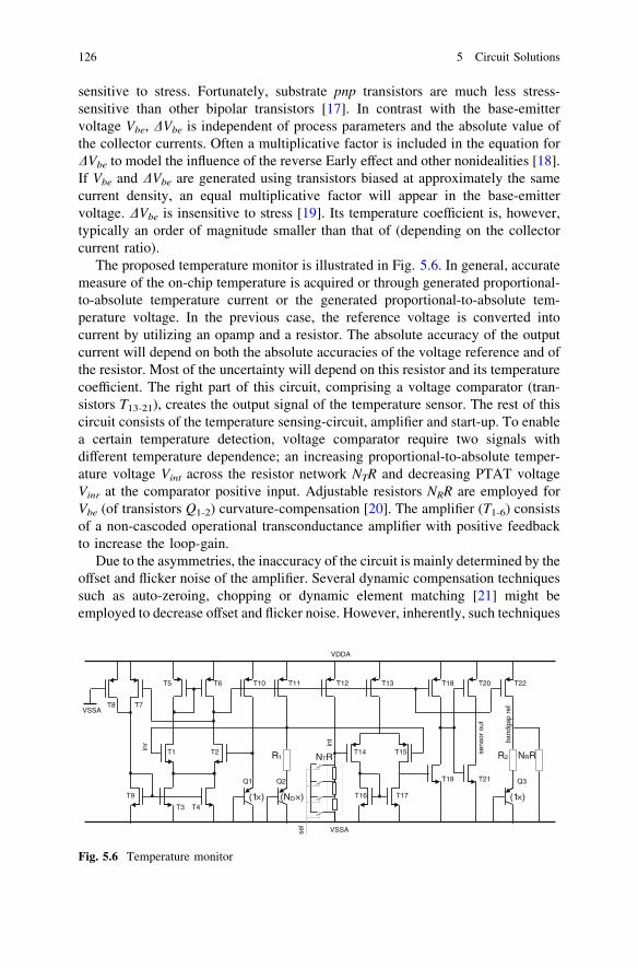
sensitive to stress. Fortunately, substrate pnp transistors are much less stress-sensitive than other bipolar transistors [17]. In contrast with the base-emittervoltage Vbe, DVbe is independent of process parameters and the absolute value ofthe collector currents. Often a multiplicative factor is included in the equation forDVbe to model the influence of the reverse Early effect and other nonidealities [18].If Vbe and DVbe are generated using transistors biased at approximately the samecurrent density, an equal multiplicative factor will appear in the base-emittervoltage. DVbe is insensitive to stress [19]. Its temperature coefficient is, however,typically an order of magnitude smaller than that of (depending on the collectorcurrent ratio).
The proposed temperature monitor is illustrated in Fig. 5.6. In general, accuratemeasure of the on-chip temperature is acquired or through generated proportional-to-absolute temperature current or the generated proportional-to-absolute tem-perature voltage. In the previous case, the reference voltage is converted intocurrent by utilizing an opamp and a resistor. The absolute accuracy of the outputcurrent will depend on both the absolute accuracies of the voltage reference and ofthe resistor. Most of the uncertainty will depend on this resistor and its temperaturecoefficient. The right part of this circuit, comprising a voltage comparator (tran-sistors T13-21), creates the output signal of the temperature sensor. The rest of thiscircuit consists of the temperature sensing-circuit, amplifier and start-up. To enablea certain temperature detection, voltage comparator require two signals withdifferent temperature dependence; an increasing proportional-to-absolute temper-ature voltage Vint across the resistor network NTR and decreasing PTAT voltageVinr at the comparator positive input. Adjustable resistors NRR are employed forVbe (of transistors Q1-2) curvature-compensation [20]. The amplifier (T1-6) consistsof a non-cascoded operational transconductance amplifier with positive feedbackto increase the loop-gain.
Due to the asymmetries, the inaccuracy of the circuit is mainly determined by theoffset and flicker noise of the amplifier. Several dynamic compensation techniquessuch as auto-zeroing, chopping or dynamic element matching [21] might beemployed to decrease offset and flicker noise. However, inherently, such techniques
VSSA
VDDA
T9
VSSA
T1
(1×)
sel
NTRR1
(ND×)
R2
(1×)
band
gap
ref
sens
or o
ut
inr in
t
T2
T3 T4
T8 T7
T5 T6 T10 T11 T12 T13
T14 T15
T16 T17
T19 T21
T18 T20
Q1 Q2 Q3
T22
NRR
Fig. 5.6 Temperature monitor
126 5 Circuit Solutions

require very fast amplifier, whose noise is typically several order of magnitude largerand consumes considerably more power. In addition, chopping ads switching noisedue to e.g. charge dump and clock interference. Such characteristics make thesetechniques unsuitable for thermal monitoring of VLSI circuits.
In this design, to lower the effect of offset, the systematic offset is minimized byadjusting transistor dimensions and bias current in the ratio, while the random offsetis reduced by a symmetrical and compact layout. Additionally, the collector currentsof bipolar transistors Q1 and Q2 are rationed by a pre-defined factor, e.g. transistorsare multiple parallel connections of unit devices. A start-up circuit consisting oftransistors T7-9 drives the circuit out of the degenerate bias point when the supply istuned on. The scan chain delivers a four-bit thermometer code for the selection of theresistor value NTR. The nodes in between each resistor have different voltagesdepending on their proximity to Vint. By using thermometer decoding on the digitalsignal one specific node can be selected as the correct analog voltage. The resistor-ladder network is inherently monotonic as long as the switching elements aredesigned correctly. Similarly, since no high-speed operation is required, parasiticcapacitors at a tap point will not create significant voltage glitch.
5.3 Characterization of Process Variability Conditions
The complexity of yield estimation, coupled with the iterative nature of the designprocess, makes yield maximization computationally prohibitive. Worst-caseanalysis is very efficient in terms of designer effort, and thus has become the mostwidely practiced technique for statistical verification. However, the worst-caseperformance values obtained are extremely pessimistic and as a result lead tounnecessarily large and power hungry designs in order to reach the desiredspecifications. In this chapter, statistical data extracted through the monitor mea-surements allow us not only possibilities to enhance observation of importantdesign and technology parameters, but to characterize current process variabilityconditions of certain parameters of interest, enabling optimized design environ-ment as well. Although, in statistics several methods, such as listwise [22] andpairwise [23] deletion and structural equation modelling [24] would provideestimates of the selected performance figures from the incomplete data, imputationmethod (e.g. substitution of some plausible value for a missing datapoint) and itsspecial case, multiple imputations based on expectation-maximization (EM)algorithm [9, 25] offers maximum likelihood estimates.
5.3.1 Optimized Design Environment
A maximum likelihood (ML) estimation involves estimation of parameter vector(threshold voltage variation, resistor width variation, etc. obtained through
5.2 Circuits for Active Monitoring of Temperature and Process Variation 127
monitor’s observation) h [ H, where H is a parameter space, for which theobserved data is the most likely, e.g. marginal probability pX|H(x|h) is a maximum,given the vector of the DLPVM’s observations xi[X, where X is a measurementspace, at temperature T. The pX|H(x|h) is the Gaussian mixture model given by theweighted sum of the Gaussian distributions. The logarithm of the probabilityp(TX|h) is referred to as the log-likehood L(h|TX) of h with respect to TX. The inputset TX is given by TX = {(x1,…,xl)}, which contains only vectors of DLPVM’sobservations xi. The log-likelihood can be factorized as
L hjTXð Þ ¼ log p TX jhð Þ ¼Xl
i¼1
X
y2Y
pXjY ;H xijyi; hð ÞpY jH yijhð Þ ð5:1Þ
for the missing data vector yi[Y, where Y is the incomplete data set, which areindependent and identically distributed according to the probability pXY|H(x,y|h).The problem of maximum likelihood estimation from the set of DLPVM obser-vations Tx can be defined as
h� ¼ maxh2H
L hjTXð Þ ¼ maxh2H
Xl
i¼1
X
y2Y
pXjY ;H xijyi; hð ÞpY jH yijhð Þ ð5:2Þ
Obtaining optimum estimates through the ML method involves two steps:computing the likelihood function and maximizing over the set of all admissiblesequences. Evaluating the contribution of the random parameter h requires com-puting an expectation over the joint statistics of the random parameter vector, atask that is analytically intractable. Even if the likelihood function L can beobtained analytically, it is invariably a nonlinear function of h, which makes themaximization step (which must be performed in real time) computationallyunfeasible. In such cases, EM algorithm [9] allows obtaining the maximum like-lihood estimates of the unknown parameters by a computational procedure whichiterates, until convergence, between two steps.
Instead of using the traditional incomplete-data density in the estimation pro-cess, the EM algorithm uses the properties of the complete-data density. In doingso, it can often make the estimation problem more tractable and also yield goodestimates of the parameters for small sample sizes [26]. Thus, with regard toimplementation, the EM algorithm holds a significant advantage over traditionalsteepest-descent methods acting on the incomplete-data likelihood equation.Moreover, the EM algorithm provides the values of the log-likelihood functioncorresponding to the maximum likelihood estimates based uniquely on theobserved data. The EM algorithm builds a sequence of parameter estimates h(0),h(1),…,h(t), such that the log-likelihood L(h(t)|TX) monotonically increases, i.e.,L(h(0)|TX) \ L(h(1)|TX) \ … \ L(h(t)|TX) until a stationary point L(h(t-1)|TX) =
L(h(t)|TX) is achieved. Using Bayes rule, the log likelihood of xi can be written as
log p TX jhð Þ ¼ log p X; Yjhð Þ; h tð Þ � log pX;Y jX X; Yjhð Þ; h tð Þ ð5:3Þ
128 5 Circuit Solutions
Taking expectations on both sides of the above equation given xi and h, whereh(t) is an available estimate of h
log p TXjhð Þ ¼ EhðtÞ log p X; Yjhð ÞjX; h tð Þf g � EhðtÞ log pX;Y jX X; Y jXð ÞjX; h tð Þffi �
¼ Qn hjhðtÞ� �
� P hjhðtÞ� �
ð5:4Þ
By Jensen’s inequality, the relation holds that
P hjhðtÞ� �
�P hðtÞjhðtÞ� �
ð5:5Þ
Therefore, a new estimate h in the next iteration step that makesQ(h(t)|h(t)) C Q(h|h(t)) leads to
log p TXjhð Þ� log p TX jhðtÞ� �
ð5:6Þ
In each iteration, two steps, called E-step and M-step are involved. In theE-step, the EM algorithm forms the auxiliary function Q(h|h(t)), (h(0),h(1),…,h(t) isa sequence of parameter estimates), which calculates the expected value of the log-likelihood function with respect to the conditional distribution Y of the functionaltest, given the vector of the DLPVM’s observations X under the current estimate ofthe parameters h(t)
Q hjhðtÞ� �
¼ E log p X; Y jhð ÞjX; h tð Þð Þ ð5:7Þ
In the M-step, the algorithm determines a new parameter maximizing Q
hðtþ1Þ ¼ arg maxh
Q hjhðtÞ� �
ð5:8Þ
At each step of the EM iteration, the likelihood function can be shown to benon-decreasing [26]; if it is also bounded (which is mostly the case in practice),then the algorithm converges. An iterative maximization of Q(h|h(t)) will lead to aML estimation of h [26].
5.3.2 Test-Limit Updates and Guidance
When an optimum estimate of the parameter distribution is obtained as describedin the previous section, the next step is to update the test limit values utilizing anadjusted support vector machine (ASVM) classifier [10]. In comparison withestablished classifiers (such as quadratic, boosting, neural networks, Bayesiannetworks), the ASVM classifier is especially resourceful, since it simultaneouslyminimizes the empirical classification error and maximizes the geometric margin.Assuming that the input vectors (e.g. values defining test limits) belong to a priori(nominal values) and a posteriori (values estimated with the EM algorithm)
5.3 Characterization of Process Variability Conditions 129
classes, the goal is to set test limits which reflect observed on-chip variation. Eachnew measurement is viewed as an r-dimensional vector and the ASVM classifierseparates the input vectors into an r-1-dimensional hyperplane in feature space
Z. Let D ¼ xi; cið ÞjxiIRr; ciI �1; 1f gffi �n
i¼1 be the input vectors belonging to a prioriand a posteriori classes, where the ci is either 1 or -1, indicating the class to whichdata xi from the input vector belongs. To maximize the margin, w and b are chosensuch that they minimize the nearest integer ||w|| subject to the optimizationproblem described by
ci w ffi xi þ bð Þ� 1 ð5:9Þ
for all 1 B i B n, where the vector w is a normal vector, which is perpendicular tothe hyperplane (e.g. defined as wffix ? b = 0). The parameter b/||w|| determine theoffset of the hyperplane from the origin along the normal vector w. In this section,we solve this optimization problem with a quadratic programming [27]. Theequation is altered by substituting ||w|| with �||w||2 without changing the solution(the minimum of the original and the modified equation have the same w and b).The quadratic programming problem is solved incrementally, covering all the sub-sets of classes constructing the optimal separating hyperplane for the full data set.Writing the classification rule in its unconstrained dual form reveals that themaximum margin hyperplane and therefore the classification task is now only afunction of the support vectors, e.g. the training data that lie on the margin
maxXn
i¼1
ai �12
X
i;j
aiajcicjxTi xj ð5:10Þ
subject to ai C 0 andPn
i¼1aici ¼ 0,
w ¼X
i
aicixi ð5:11Þ
where the a terms constitute the weight vector in terms of the training set. To allowfor mislabeled examples a modified maximum margin technique [27] is employed.If there exists no hyperplane that can divide the a priori and a posteriori classes,the modified maximum margin technique finds a hyperplane that separates thetraining set with a minimal number of errors. The method introduces non-negativevariables ni, which measure the degree of misclassification of the data xi
ci w ffi xi þ bð Þ� 1� ni ð5:12Þ
for all 1 B i B n. The objective function is then increased by a function whichpenalizes non-zero ni, and the optimization becomes a trade-off between a largemargin and a small error penalty. For a linear penalty function, the optimizationproblem now transforms to
min12
wk k2þCX
i
nri ð5:13Þ
130 5 Circuit Solutions
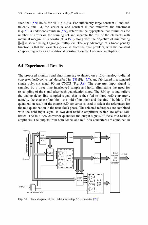
such that (5.9) holds for all 1 B i B n. For sufficiently large constant C and suf-ficiently small r, the vector w and constant b that minimize the functional(Eq. 5.13) under constraints in (5.9), determine the hyperplane that minimizes thenumber of errors on the training set and separate the rest of the elements withmaximal margin. This constraint in (5.9) along with the objective of minimizing||w|| is solved using Lagrange multipliers. The key advantage of a linear penaltyfunction is that the variables ni vanish from the dual problem, with the constantC appearing only as an additional constraint on the Lagrange multipliers.
5.4 Experimental Results
The proposed monitors and algorithms are evaluated on a 12-bit analog-to-digitalconverter (A/D converter) described in [28] (Fig. 5.7), and fabricated in a standardsingle poly, six metal 90 nm CMOS (Fig. 5.8). The converter input signal issampled by a three-time interleaved sample-and-hold, eliminating the need forre-sampling of the signal after each quantization stage. The S/H splits and buffersthe analog delay line sampled signal that is then fed to three A/D converters,namely, the coarse (four bits), the mid (four bits) and the fine (six bits). Thequantization result of the coarse A/D converter is used to select the references forthe mid quantization in the next clock phase. The selected references are combinedwith the held input signal in two dual-residue amplifiers, which are offset cali-brated. The mid A/D converter quantizes the output signals of these mid-residueamplifiers. The outputs from both coarse and mid A/D converters are combined in
4-bitCoarseADC
3 Interleaved S/H
12 BIT
INPUT
DigitalDecoder
andError
Correction
VRT
VRB
Ref
eren
ce L
adde
r Latch
SwitchMatrix Res
Amps
4-bitMidADC
Latch
Latch
SwitchMatrix Res
Amps
6-bitFineADC
Fig. 5.7 Block diagram of the 12-bit multi-step A/D converter [28]
5.3 Characterization of Process Variability Conditions 131
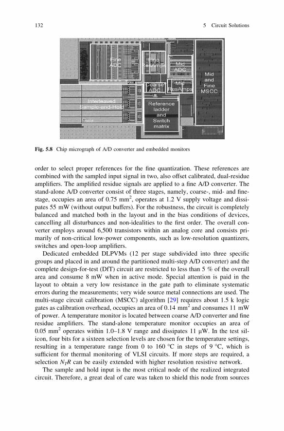
order to select proper references for the fine quantization. These references arecombined with the sampled input signal in two, also offset calibrated, dual-residueamplifiers. The amplified residue signals are applied to a fine A/D converter. Thestand-alone A/D converter consist of three stages, namely, coarse-, mid- and fine-stage, occupies an area of 0.75 mm2, operates at 1.2 V supply voltage and dissi-pates 55 mW (without output buffers). For the robustness, the circuit is completelybalanced and matched both in the layout and in the bias conditions of devices,cancelling all disturbances and non-idealities to the first order. The overall con-verter employs around 6,500 transistors within an analog core and consists pri-marily of non-critical low-power components, such as low-resolution quantizers,switches and open-loop amplifiers.
Dedicated embedded DLPVMs (12 per stage subdivided into three specificgroups and placed in and around the partitioned multi-step A/D converter) and thecomplete design-for-test (DfT) circuit are restricted to less than 5 % of the overallarea and consume 8 mW when in active mode. Special attention is paid in thelayout to obtain a very low resistance in the gate path to eliminate systematicerrors during the measurements; very wide source metal connections are used. Themulti-stage circuit calibration (MSCC) algorithm [29] requires about 1.5 k logicgates as calibration overhead, occupies an area of 0.14 mm2 and consumes 11 mWof power. A temperature monitor is located between coarse A/D converter and fineresidue amplifiers. The stand-alone temperature monitor occupies an area of0.05 mm2 operates within 1.0–1.8 V range and dissipates 11 lW. In the test sil-icon, four bits for a sixteen selection levels are chosen for the temperature settings,resulting in a temperature range from 0 to 160 �C in steps of 9 �C, which issufficient for thermal monitoring of VLSI circuits. If more steps are required, aselection NTR can be easily extended with higher resolution resistive network.
The sample and hold input is the most critical node of the realized integratedcircuit. Therefore, a great deal of care was taken to shield this node from sources
Fig. 5.8 Chip micrograph of A/D converter and embedded monitors
132 5 Circuit Solutions
of interference. The total sample-and-hold consists of three identical interleavedsample-and-hold units. S/H units, input signals, critical clock lines and outputsignal lines have been all provided with shielding and routed as short and sym-metrical as possible. The switch unit is placed near the reference ladder to reducethe resistor-ladder D/A converter settling time. Selected reference signals from theswitch unit are routed as short as possible, since the delay due to the wiringcapacitance increases the residue amplifier settling time. The delay due to thewiring capacitance causes residue amplifier to momentarily develop its output inthe wrong direction until the correct selection switch closes. After the correctswitch is selected, the output starts to converge in the correct direction. Therefore,the wiring capacitance increases the residue amplifier settling time due to thewires. If reference ladder is placed nearer, the reference signals for the compar-ators could be easily corrupted due to the coupling of the large digital signalstraveling nearby. The preamplifier are laid out in a linear array and connected tothe comparator array by abutment. The comparator array must align with pre-amplifiers, implying that high aspect ratio is necessary for the comparator layout.Locating these arrays close to each other greatly reduces wiring capacitanceproviding maximum speed. To keep the comparator array small and the wiresshort, data is driven out of the array immediately after amplification to full swing.
Clocks are distributed from right to left, to partially cancel the sample timevariation with reference level that increases from left to right. The comparatorswith complementary clocks are interleaved, sharing the same input, reference andsupply wires so that charge kickback and supply noise are cancelled to first order.
The clock lines are routed in the center of the active area where the appropriatephases are tapped off at the location of each stage in the circuit. Digital correctionis at the lower right corner of the active area; and 12 bits output is produced at thepads on the bottom. Extra digital circuitry is added on the right, along with somedummy metal lines for process yield purposes. The differential circuit topology isused throughout the design and multiple substrate taps are placed close to the noisesensitive circuits to avoid the noise injection. For analog blocks, substrate taps areplaced close to the n-channel transistors and connected to an analog ground nearby(for common-source configuration, substrate taps are connected to the source). Fordigital blocks, substrate taps are placed close to n-channel transistors and con-nected to a separate substrate pin to a dedicated output pad. This pad is then joinedwith ground on the evaluation board. An added advantage for placing substratetaps close or next to transistors is to minimize the body effect variation. Forcommon-source devices, no body effect is found since the source and body areconnected. For cascode devices, although the source potential may vary withrespect to the body potential, the effect of VT on the drain current is greatly reduceddue to the source degeneration. No additional substrate taps are placed to avoidthat they act as noise receptors to couple extra noise into the circuit.
Separate VDD and ground pins are used for each functional block not only tominimize the noise coupling between different circuit blocks, but also to reduce theoverall impedance to ground. Multiple VDD and ground pins are used throughoutthe chip. The digital VDD and ground pins are separated from the analog ones.
5.4 Experimental Results 133
Within the analog section, VDD and ground pins for different functional blocks arealso separated to have more flexibility during the experiment. Each supply pin isconnected to a Hewlett-Packard HP3631A voltage regulator and is also bypassedto ground with a 10 lF Tantalum capacitor and a 0.1 lF Ceramic chip capacitor.The reference current sources are generated by Keithley 224 external currentsource. For the experiment, the sinusoidal input signal is generated by an arbitrarywaveform generator (Tektronix AWG2021) and applied at the first to a narrow,band-pass filter to remove any harmonic distortion and extraneous noise, and thento the test board. The signal is connected via 50 X coaxial cables to minimizeexternal interference. On the test circuit board, the single-ended signal is convertedto a balanced, differential signal using a transformer (Mini-Circuit PSCJ-2-1).
The outputs of the transformer are dc level-shifted to a common-mode inputvoltage and terminated with two 50 X matching resistors. The common-modevoltage of the test signal going into the A/D converter is set through matchingresistors connected to a voltage reference. The digital output of the A/D converteris buffered with an output buffer to the drive large parasitic capacitance of the lineson the board and probes from the logic analyzer. The digital outputs are capturedby the logic analyzer (Agilent 1682AD). A clock signal is also provided to the logicanalyzer to synchronize with the A/D converter. All the equipment is set by aLabView program and signal analysis is performed with MatLab. A clock signal isalso provided to the logic analyzer to synchronize with the A/D converter.Repetitive single die-level process monitor measurements are performed to min-imize noise errors. Special attention is paid in the layout to obtain a very lowresistance in the gate path to eliminate systematic errors during the measurements;very wide source metal connections are used. Since different transistors aremeasured sequentially the dc repeatability of the dc gate voltage source must belarger than the smallest gate-voltage offset to be measured. The repeatability of thesource in the measurement set-up was better than six digits. All chips are func-tional in a temperature range between 0 and 160 �C.
Before proceeding with evaluating an A/D converter performance, firstly ameasure of error, e.g. an estimator of the loss function, is introduced. A qualitycriterion is generally speaking a function that given the input and output to asystem calculates the deviation inflicted by the system. Most common qualitycriterion measures are based on the distance between the output and the input, andare therefore denoted distance measures. That is, the deviation is a function of theabsolute difference between output and input, and not of the input or outputthemselves. In the multi-dimensional case this corresponds to the deviation being afunction of the norm (length) of the difference vector. Two commonly used dis-tance measures are the absolute error and the squared error.
The quality criterion usually adopted for an estimator of the loss function is themean-squared error criterion, mainly because it represents the energy in the errorsignal, is easy to differentiate and provides the possibilities to assign the weights.Although the mean-squared error criterion is very commonly used, especially froma signal processing point of view, other criteria can be considered. From an A/Dconverter characterization point of view one, the reconstruction levels might be
134 5 Circuit Solutions
considered to be an inherent parameter of the A/D converter under test and not ofthe input signal as was the case in the mean-squared error criterion. The midpointstrategy is based on the assumption that the A/D converter acts as a staircasequantizer, e.g. the reconstruction value associated with a specific quantizationregion should be the midpoint of that region. If the quantization regions shoulddeviate from the ideal ones, then the output values should be changed accordingly.The midpoint approach is consistent with mean-squared error criterion approach ifeach quantization region is symmetric. Two such signals are the uniform noise andthe deterministic ramp, which provide symmetric PDFs within each quantizationregion, save the regions at the extremes of the signal range where the signal mayoccupy only part of the region. In the minimum harmonic estimation method[30, 31], on the other hand, estimation values are selected in such a way that theharmonic distortion generated by the A/D converter is minimized. The methoduses single sinewaves, and the estimation tables are built using error basis func-tions, usually two-dimensional Gaussian basis functions in a phase-plane indexingscheme. The basis function coefficients are selected using minimization of thepower in the selected number of first harmonics to the test frequency. Theestimation values dependent not only on the characteristics of the A/D converterunder test, but also on the test signal itself (through the probability density functionof the signal).
It is therefore of vital importance that the estimation routine is carefullydesigned as it can yield an estimation system that is heavily biased towards aspecific signal, since the estimation values were trained using that signal type. Onthe other hand, if prior knowledge says that the A/D converter will be used toconvert signals of a specific class, it is straightforward to evaluate the system usingthe same class of signals. Using estimation signals with a uniform probabilitydensity function can be considered to lead to unbiased calibration results. In thiscase, both mean-squared and midpoint strategy, coincide. Although, there aremany specific measures for describing the performance of an A/D converter–signal-to-noise-and-distortion ratio, spurious-free dynamic range, effective numberof bits, total harmonic distortion, etc. which assess the precision and quality ofA/D converters, most of the specialized measures result in fairly complicatedexpressions that do not provide results of practical use. Exceptions are signal-to-noise-and-distortion ratio and effective number of bits which are both closelyrelated to the mean-squared error criterion; therefore, most results expressed asmean-squared error can be transferred to results on signal-to-noise-and-distortionratio and effective number of bits as shown in Appendix C.
A wide variety of calibration techniques to minimize or correct the stepscausing discontinuities in the A/D converter’s stage transfer functions has beenproposed [32–43]. The mismatch and error attached to each step can either beaveraged out, or their magnitude can be measured and corrected. Analog cali-bration methods include in this context the techniques in which adjusting orcompensation of component values is performed with analog circuitry, while thecalculation and storing of the correction coefficient can be digital. However, digitalmethods have gained much more popularity, mainly because of the increased
5.4 Experimental Results 135
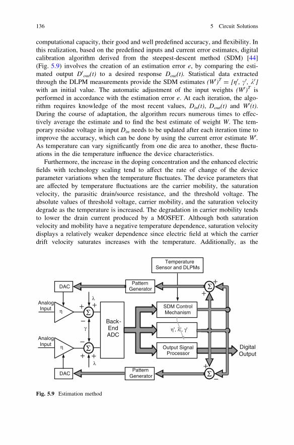
computational capacity, their good and well predefined accuracy, and flexibility. Inthis realization, based on the predefined inputs and current error estimates, digitalcalibration algorithm derived from the steepest-descent method (SDM) [44](Fig. 5.9) involves the creation of an estimation error e, by comparing the esti-mated output D0out(t) to a desired response Dout(t). Statistical data extractedthrough the DLPM measurements provide the SDM estimates (W0)T = [g0, c0, k0]with an initial value. The automatic adjustment of the input weights (W0)T isperformed in accordance with the estimation error e. At each iteration, the algo-rithm requires knowledge of the most recent values, Din(t), Dout(t) and W0(t).During the course of adaptation, the algorithm recurs numerous times to effec-tively average the estimate and to find the best estimate of weight W. The tem-porary residue voltage in input Din needs to be updated after each iteration time toimprove the accuracy, which can be done by using the current error estimate W0.As temperature can vary significantly from one die area to another, these fluctu-ations in the die temperature influence the device characteristics.
Furthermore, the increase in the doping concentration and the enhanced electricfields with technology scaling tend to affect the rate of change of the deviceparameter variations when the temperature fluctuates. The device parameters thatare affected by temperature fluctuations are the carrier mobility, the saturationvelocity, the parasitic drain/source resistance, and the threshold voltage. Theabsolute values of threshold voltage, carrier mobility, and the saturation velocitydegrade as the temperature is increased. The degradation in carrier mobility tendsto lower the drain current produced by a MOSFET. Although both saturationvelocity and mobility have a negative temperature dependence, saturation velocitydisplays a relatively weaker dependence since electric field at which the carrierdrift velocity saturates increases with the temperature. Additionally, as the
Back-EndADC
SDM Control Mechanism
Output Signal Processor
DAC
DAC Σ
Σ
+
−
++
DigitalOutput
TemperatureSensor and DLPMs
η , λ’, γ’
PatternGenerator
PatternGenerator
Σ
λ
γ
η
Σ
λ
η+ +
++
−
−
Analog Input
Analog Input
Fig. 5.9 Estimation method
136 5 Circuit Solutions
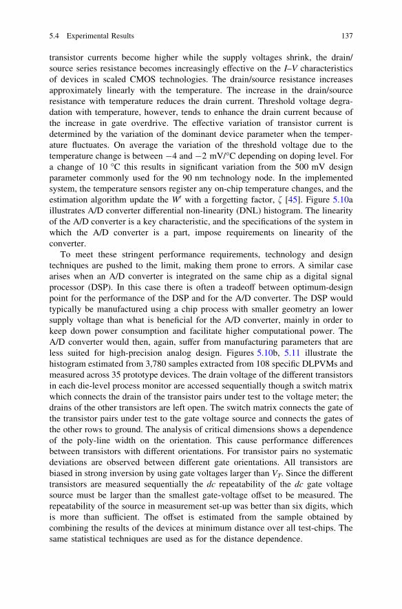
transistor currents become higher while the supply voltages shrink, the drain/source series resistance becomes increasingly effective on the I–V characteristicsof devices in scaled CMOS technologies. The drain/source resistance increasesapproximately linearly with the temperature. The increase in the drain/sourceresistance with temperature reduces the drain current. Threshold voltage degra-dation with temperature, however, tends to enhance the drain current because ofthe increase in gate overdrive. The effective variation of transistor current isdetermined by the variation of the dominant device parameter when the temper-ature fluctuates. On average the variation of the threshold voltage due to thetemperature change is between -4 and -2 mV/�C depending on doping level. Fora change of 10 �C this results in significant variation from the 500 mV designparameter commonly used for the 90 nm technology node. In the implementedsystem, the temperature sensors register any on-chip temperature changes, and theestimation algorithm update the W0 with a forgetting factor, f [45]. Figure 5.10aillustrates A/D converter differential non-linearity (DNL) histogram. The linearityof the A/D converter is a key characteristic, and the specifications of the system inwhich the A/D converter is a part, impose requirements on linearity of theconverter.
To meet these stringent performance requirements, technology and designtechniques are pushed to the limit, making them prone to errors. A similar casearises when an A/D converter is integrated on the same chip as a digital signalprocessor (DSP). In this case there is often a tradeoff between optimum-designpoint for the performance of the DSP and for the A/D converter. The DSP wouldtypically be manufactured using a chip process with smaller geometry an lowersupply voltage than what is beneficial for the A/D converter, mainly in order tokeep down power consumption and facilitate higher computational power. TheA/D converter would then, again, suffer from manufacturing parameters that areless suited for high-precision analog design. Figures 5.10b, 5.11 illustrate thehistogram estimated from 3,780 samples extracted from 108 specific DLPVMs andmeasured across 35 prototype devices. The drain voltage of the different transistorsin each die-level process monitor are accessed sequentially though a switch matrixwhich connects the drain of the transistor pairs under test to the voltage meter; thedrains of the other transistors are left open. The switch matrix connects the gate ofthe transistor pairs under test to the gate voltage source and connects the gates ofthe other rows to ground. The analysis of critical dimensions shows a dependenceof the poly-line width on the orientation. This cause performance differencesbetween transistors with different orientations. For transistor pairs no systematicdeviations are observed between different gate orientations. All transistors arebiased in strong inversion by using gate voltages larger than VT. Since the differenttransistors are measured sequentially the dc repeatability of the dc gate voltagesource must be larger than the smallest gate-voltage offset to be measured. Therepeatability of the source in measurement set-up was better than six digits, whichis more than sufficient. The offset is estimated from the sample obtained bycombining the results of the devices at minimum distance over all test-chips. Thesame statistical techniques are used as for the distance dependence.
5.4 Experimental Results 137
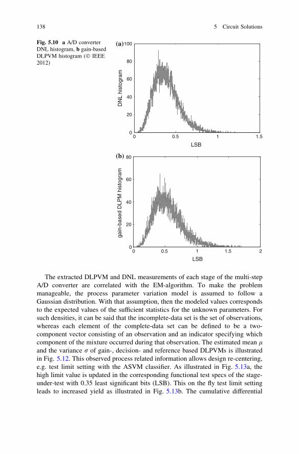
The extracted DLPVM and DNL measurements of each stage of the multi-stepA/D converter are correlated with the EM-algorithm. To make the problemmanageable, the process parameter variation model is assumed to follow aGaussian distribution. With that assumption, then the modeled values correspondsto the expected values of the sufficient statistics for the unknown parameters. Forsuch densities, it can be said that the incomplete-data set is the set of observations,whereas each element of the complete-data set can be defined to be a two-component vector consisting of an observation and an indicator specifying whichcomponent of the mixture occurred during that observation. The estimated mean land the variance r of gain-, decision- and reference based DLPVMs is illustratedin Fig. 5.12. This observed process related information allows design re-centering,e.g. test limit setting with the ASVM classifier. As illustrated in Fig. 5.13a, thehigh limit value is updated in the corresponding functional test specs of the stage-under-test with 0.35 least significant bits (LSB). This on the fly test limit settingleads to increased yield as illustrated in Fig. 5.13b. The cumulative differential
0 0.5 1 1.50
20
40
60
80
100
LSB
DN
L hi
stog
ram
0 0.5 1 1.5 20
20
40
60
80
LSB
gain
-bas
ed D
LPM
his
togr
am
(a)
(b)
Fig. 5.10 a A/D converterDNL histogram, b gain-basedDLPVM histogram (� IEEE2012)
138 5 Circuit Solutions
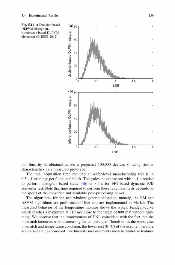
non-linearity is obtained across a projected 100,000 devices showing similarcharacteristics as a measured prototype.
The total acquisition time required at wafer-level manufacturing test is in0.5*1 ms range per functional block. This pales in comparison with *1 s neededto perform histogram-based static [46] or *1 s for FFT-based dynamic A/Dconverter test. Note that time required to perform these functional tests depends onthe speed of the converter and available post-processing power.
The algorithms for the test window generation/update, namely, the EM andASVM algorithms are performed off-line and are implemented in Matlab. Themeasured behavior of the temperature monitor shows the typical bandgap-curvewhich reaches a maximum at 810 mV close to the target of 800 mV without trim-ming. We observe that the improvement of DNL coincident with the fact that themismatch increases when decreasing the temperature. Therefore, as the worst casemismatch and temperature condition, the lower end (0 �C) of the used temperaturescale (0–90 �C) is observed. The linearity measurements show bathtub-like features
0 0.5 1 1.5 20
20
40
60
80
LSB
deci
sion
-bas
ed D
LPM
his
togr
am
0 0.5 1 1.5 20
20
40
60
80
LSB
refe
renc
e-ba
sed
DLP
M h
isto
gram
(a)
(b)
Fig. 5.11 a Decision-basedDLPVM histogram,b reference-based DLPVMhistogram (� IEEE 2012)
5.4 Experimental Results 139
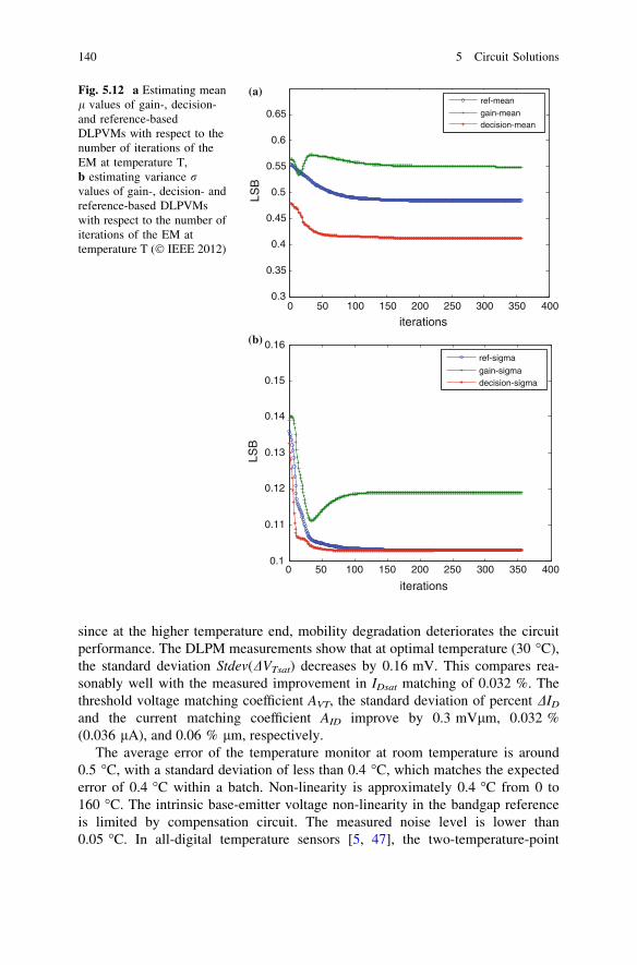
since at the higher temperature end, mobility degradation deteriorates the circuitperformance. The DLPM measurements show that at optimal temperature (30 �C),the standard deviation Stdev(DVTsat) decreases by 0.16 mV. This compares rea-sonably well with the measured improvement in IDsat matching of 0.032 %. Thethreshold voltage matching coefficient AVT, the standard deviation of percent DID
and the current matching coefficient AID improve by 0.3 mVlm, 0.032 %(0.036 lA), and 0.06 % lm, respectively.
The average error of the temperature monitor at room temperature is around0.5 �C, with a standard deviation of less than 0.4 �C, which matches the expectederror of 0.4 �C within a batch. Non-linearity is approximately 0.4 �C from 0 to160 �C. The intrinsic base-emitter voltage non-linearity in the bandgap referenceis limited by compensation circuit. The measured noise level is lower than0.05 �C. In all-digital temperature sensors [5, 47], the two-temperature-point
0 50 100 150 200 250 300 350 4000.3
0.35
0.4
0.45
0.5
0.55
0.6
0.65
iterations
LSB
ref-mean
gain-meandecision-mean
0 50 100 150 200 250 300 350 4000.1
0.11
0.12
0.13
0.14
0.15
0.16
iterations
LSB
ref-sigma
gain-sigmadecision-sigma
(a)
(b)
Fig. 5.12 a Estimating meanl values of gain-, decision-and reference-basedDLPVMs with respect to thenumber of iterations of theEM at temperature T,b estimating variance rvalues of gain-, decision- andreference-based DLPVMswith respect to the number ofiterations of the EM attemperature T (� IEEE 2012)
140 5 Circuit Solutions
calibration is required in every sensor; thus, calibration cost is very large inon-chip thermal sensing applications.
A current-output temperature sensor [6] does not have a linear temperaturereading and is sensitive to process variation, which requires more effort and costfor after-process calibration. Although the dual-DLL-based temperature sensor[48] only needs one-temperature-point calibration, it occupies large chip area witha high level of power consumption at a microwatt level. The sensors based on thetemperature characteristics of parasitic bipolar transistors [49, 50] offer highaccuracy and small chip area. However, high power consumption in [49] and smalltemperature range in [50] make these realizations unsuitable for on-chip thermalmonitoring.
The key to evaluate the performance of the multi-step A/D converter is to selectand separate the information from the transfer function. For at-speed testing of theanalog performance of the A/D converter it is not only imperative to have all 12digital outputs and the two out of range signals available at the device pins, but toperform performance evaluation of each stage, the output signals of the coarse,mid and fine A/D converters need to be observable too. Measuring of the circuitperformance of each stage is executed sequentially starting from the first stage, e.g.each stage is evaluated separately—at a lower speed—enabling the use of standardindustrial analog waveform generators. To allow coherent testing, the clock signalof the A/D converter has to be fully controllable by the tester at all times. Addingall these requests together leads to an output test bus that needs to be 14 bits wide.The connections of the test bus are not only restricted to the test of the analog part.For digital testing the test bus is also used to carry digital data from scan chains.The test-shell [51] contains all functional control logic, the digital test-bus, a testcontrol block (TCB) and a CTAG isolation chain for digital input/output to andfrom other IP/cores. Further, logic necessary for creating certain control signals forthe analog circuit parts, and for the scan-chains a bypass mechanism, controlled bythe test control block, is available as well.
In the coarse A/D converter, process variations of the analog componentsinternal to the converter cause deviation, from ideal, of the transfer function of thecoarse A/D converter by changing the step sizes in the transfer function. Thesecases, which include resistor value, comparator’s offset and comparator’s biascurrent out of specification result in different patterns. The number of peaks andthe location of the peak data identify the type and the location. Since there is nofeedback from mid and fine A/D converters to the coarse result value, it is notnecessary to set these two A/D converters at the fixed value to test coarse A/D.Calibration D/A converter settings do not show in coarse A/D converter results;the calibration system however should remain operative. Random calibrationcycles are not allowed to prevent interference with measured results. The responseof the mid A/D converter cannot directly be tested using the normal A/D converteroutput data due to an overlap in the A/D converter ranges. Nevertheless, by settingthe coarse exor output signals using the scan chain through this block, knownvalues are assigned to the mid switch. The residue signals are now used to verifythe mid A/D converter separately by observing the mid A/D converter output bits
5.4 Experimental Results 141
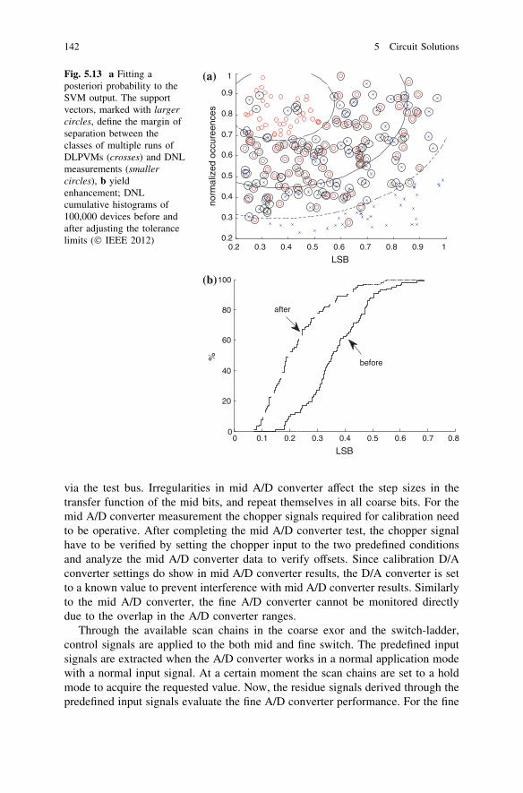
via the test bus. Irregularities in mid A/D converter affect the step sizes in thetransfer function of the mid bits, and repeat themselves in all coarse bits. For themid A/D converter measurement the chopper signals required for calibration needto be operative. After completing the mid A/D converter test, the chopper signalhave to be verified by setting the chopper input to the two predefined conditionsand analyze the mid A/D converter data to verify offsets. Since calibration D/Aconverter settings do show in mid A/D converter results, the D/A converter is setto a known value to prevent interference with mid A/D converter results. Similarlyto the mid A/D converter, the fine A/D converter cannot be monitored directlydue to the overlap in the A/D converter ranges.
Through the available scan chains in the coarse exor and the switch-ladder,control signals are applied to the both mid and fine switch. The predefined inputsignals are extracted when the A/D converter works in a normal application modewith a normal input signal. At a certain moment the scan chains are set to a holdmode to acquire the requested value. Now, the residue signals derived through thepredefined input signals evaluate the fine A/D converter performance. For the fine
0.2 0.3 0.4 0.5 0.6 0.7 0.8 0.9 10.2
0.3
0.4
0.5
0.6
0.7
0.8
0.9
1
LSB
norm
aliz
ed o
ccur
eenc
es
0 0.1 0.2 0.3 0.4 0.5 0.6 0.7 0.80
20
40
60
80
100
LSB
%
after
before
(a)
(b)
Fig. 5.13 a Fitting aposteriori probability to theSVM output. The supportvectors, marked with largercircles, define the margin ofseparation between theclasses of multiple runs ofDLPVMs (crosses) and DNLmeasurements (smallercircles), b yieldenhancement; DNLcumulative histograms of100,000 devices before andafter adjusting the tolerancelimits (� IEEE 2012)
142 5 Circuit Solutions
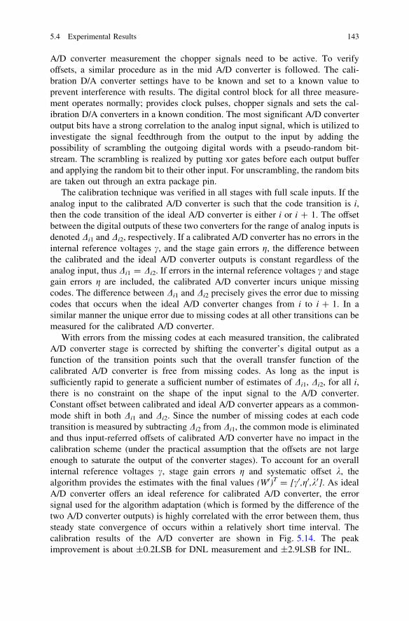
A/D converter measurement the chopper signals need to be active. To verifyoffsets, a similar procedure as in the mid A/D converter is followed. The cali-bration D/A converter settings have to be known and set to a known value toprevent interference with results. The digital control block for all three measure-ment operates normally; provides clock pulses, chopper signals and sets the cal-ibration D/A converters in a known condition. The most significant A/D converteroutput bits have a strong correlation to the analog input signal, which is utilized toinvestigate the signal feedthrough from the output to the input by adding thepossibility of scrambling the outgoing digital words with a pseudo-random bit-stream. The scrambling is realized by putting xor gates before each output bufferand applying the random bit to their other input. For unscrambling, the random bitsare taken out through an extra package pin.
The calibration technique was verified in all stages with full scale inputs. If theanalog input to the calibrated A/D converter is such that the code transition is i,then the code transition of the ideal A/D converter is either i or i ? 1. The offsetbetween the digital outputs of these two converters for the range of analog inputs isdenoted Di1 and Di2, respectively. If a calibrated A/D converter has no errors in theinternal reference voltages c, and the stage gain errors g, the difference betweenthe calibrated and the ideal A/D converter outputs is constant regardless of theanalog input, thus Di1 = Di2. If errors in the internal reference voltages c and stagegain errors g are included, the calibrated A/D converter incurs unique missingcodes. The difference between Di1 and Di2 precisely gives the error due to missingcodes that occurs when the ideal A/D converter changes from i to i ? 1. In asimilar manner the unique error due to missing codes at all other transitions can bemeasured for the calibrated A/D converter.
With errors from the missing codes at each measured transition, the calibratedA/D converter stage is corrected by shifting the converter’s digital output as afunction of the transition points such that the overall transfer function of thecalibrated A/D converter is free from missing codes. As long as the input issufficiently rapid to generate a sufficient number of estimates of Di1, Di2, for all i,there is no constraint on the shape of the input signal to the A/D converter.Constant offset between calibrated and ideal A/D converter appears as a common-mode shift in both Di1 and Di2. Since the number of missing codes at each codetransition is measured by subtracting Di2 from Di1, the common mode is eliminatedand thus input-referred offsets of calibrated A/D converter have no impact in thecalibration scheme (under the practical assumption that the offsets are not largeenough to saturate the output of the converter stages). To account for an overallinternal reference voltages c, stage gain errors g and systematic offset k, thealgorithm provides the estimates with the final values (W0)T = [c0,g0,k0]. As idealA/D converter offers an ideal reference for calibrated A/D converter, the errorsignal used for the algorithm adaptation (which is formed by the difference of thetwo A/D converter outputs) is highly correlated with the error between them, thussteady state convergence of occurs within a relatively short time interval. Thecalibration results of the A/D converter are shown in Fig. 5.14. The peakimprovement is about ±0.2LSB for DNL measurement and ±2.9LSB for INL.
5.4 Experimental Results 143
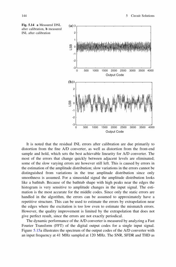
It is noted that the residual INL errors after calibration are due primarily todistortion from the fine A/D converter, as well as distortion from the front-endsample and hold, which sets the best achievable linearity for A/D converter. Themost of the errors that change quickly between adjacent levels are eliminated;some of the slow varying errors are however still left. This is caused by errors inthe estimation of the amplitude distribution; slow variations in the errors cannot bedistinguished from variations in the true amplitude distribution since onlysmoothness is assumed. For a sinusoidal signal the amplitude distribution lookslike a bathtub. Because of the bathtub shape with high peaks near the edges thehistogram is very sensitive to amplitude changes in the input signal. The esti-mation is the most accurate for the middle codes. Since only the static errors arehandled in the algorithm, the errors can be assumed to approximately have arepetitive structure. This can be used to estimate the errors by extrapolation nearthe edges where the excitation is too low even to estimate the mismatch errors.However, the quality improvement is limited by the extrapolation that does notgive perfect result, since the errors are not exactly periodical.
The dynamic performance of the A/D converter is measured by analyzing a FastFourier Transform (FFT) of the digital output codes for a single input signal.Figure 5.15a illustrates the spectrum of the output codes of the A/D converter withan input frequency at 41 MHz sampled at 120 MHz. The SNR, SFDR and THD as
0 500 1000 1500 2000 2500 3000 3500 4000-3
-2
-1
0
1
2
3
Output CodeLS
B
0 500 1000 1500 2000 2500 3000 3500 4000-3
-2
-1
0
1
2
3
Output Code
LSB
(a)
(b)
Fig. 5.14 a Measured DNLafter calibration, b measuredINL after calibration
144 5 Circuit Solutions
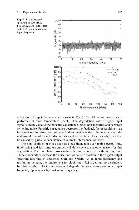
a function of input frequency are shown in Fig. 5.15b. All measurements wereperformed at room temperature (25 �C). The degradation with a higher inputsignal is mainly due to the parasitic capacitance, clock non-idealities and substrateswitching noise. Parasitic capacitance decreases the feedback factor resulting in anincreased settling time constant. Clock skew, which is the difference between thereal arrival time of a clock edge and its ideal arrival time of a clock edge, can alsobe caused by parasitic capacitance of a clock interconnection wire.
The non-idealities of clock such as clock jitter, non-overlapping period time,finite rising and fall time, unsymmetrical duty cycle are another reason for thisdegradation. The three latter errors reduce the time allocated for the setting time.These errors either increase the noise floor or cause distortion in the digital outputspectrum resulting in decreased SNR and SNDR. As an input frequency andresolution increase, the requirement for clock jitter [52] is getting more stringent.In other words, a clock jitter error will degrade the SNR even more as an inputfrequency approaches Nyquist input frequency.
-100
-80
-60
-40
-20
0
20
40
60
80
0 20 40 60 80 100 120 140 16055
60
65
70
75
80
85
90
Signal frequency [MHz]
SF
DR
, TH
D, S
NR
[dB
] SFDRTHDSNR
Signal frequency [MHz]
Mag
nitu
de [d
B]
10 300 20 40 50 60
(a)
(b)
Fig. 5.15 a Measuredspectrum at 120 MS/s,b measurement SNR, THDand SFDR as a function ofinput frequency
5.4 Experimental Results 145
5.5 Conclusions
The feasibility of the method has been verified by experimental measurementsfrom the silicon prototype fabricated in standard single poly, six metal 90 nmCMOS. The monitors allow the readout of local (within the core) performanceparameters as well as the global distribution of these parameters significantlyincreasing obtained yield. The monitors are small, stand alone and easily scalable,and can be fully switched off. The flexibility of the concept allows the system to beeasily extended with a variety of other performance monitors. The implementedexpectation-maximization algorithm and adjusted support vector machine classi-fier allow us to guide the verification process with the information obtainedthrough monitoring process variations. Fast identification of excessive processparameter and temperature variation effects is facilitated at the cost of at most 5 %area overhead and 8 mW of power consumption when in active mode.
References
1. ITRS, International Technology Roadmap for Semiconductors (2009)2. V. Petrescu, M. Pelgrom, H. Veendrick, P. Pavithran, J. Wieling, Monitors for a signal
integrity measurement system, in Proceedings of IEEE European Solid-State CircuitConference, 2006, pp. 122–125
3. M. Bhushan, M.B. Ketchen, S. Polonksy, A. Gattiker, Ring oscillator based technique formeasuring variability statistics, in Proceedings of IEEE International Conference onMicroelectronic Test Structures, 2006, pp. 87–92
4. N. Izumi et al., Evaluation of transistor property variations within chips on 300 mm wafersusing a new MOSFET array test structure. IEEE Trans. Semicond. Manuf. 17(3), 248–254(2004)
5. P. Chen, C. Chen, C. Tsai, W. Lu, A time-to-digital-converter based CMOS smarttemperature sensor. IEEE J. Solid-State Circ. 40(8), 1642–1648 (2005)
6. V. Szekely, C. Marta, Z. Kohari, M. Rencz, CMOS sensors for online thermal monitoring ofVLSI circuits. IEEE Trans. VLSI Syst. 5(3), 270–276 (1997)
7. B. Datta, W. Burleson, Temperature effects on energy optimization in sub-threshold circuitdesign, in Proceedings of IEEE International Symposium on Quality Electronic Design,2009, pp. 680–685
8. G.C.M. Meijer, G. Wang, F. Fruett, Temperature sensors and voltage references implementedin CMOS technology. IEEE Sens. J. 1(3), 225–234 (2001)
9. G.J. McLachlan, T. Krishnan, The EM Algorithm and Extensions, (Wiley-Interscience,New York, 1997)
10. C. Cortes, V. Vapnik, Support-vector networks. Machine Learning 20, 273–297 (1995)11. IEEE Standard Test Access Port and Boundary-Scan Architecture, IEEE Std. 1149.1-2001,
Test Technol. Tech. Committee. IEEE Computer Soc12. E. Sackinger, W. Guggenuhl, A high-swing, high-impedance MOS cascode circuit. IEEE J.
Solid-State Circ. 25(1), 89–298 (1990)13. P. Coban, A. Allen, 1.75-V rail-to-rail CMOS opamp, in Proceedings of IEEE International
Symposium on Circuits and Systems, 1994, vol. 5, pp. 497–50014. T. Kumamoto, M. Nakaya, H. Honda, S. Asai, Y. Akasaka, Y. Horiba, An 8-bit high-speed
CMOS A/D converter. IEEE J. Solid-State Circ. 21(6), 976–982 (1986)
146 5 Circuit Solutions
15. A. Yukawa, An 8-bit high-speed CMOS A/D converter, IEEE J. Solid-State Circuits, 20(3),775–779 (1985)
16. C–.C. Huang, J.-T. Wu, A background comparator calibration technique for flash analog-to-digital converters. IEEE Trans. Circ. Syst. I 52(9), 1732–1740 (2005)
17. F. Fruett, G.C.M. Meijer, A. Bakker, Minimization of the mechanical-stress-inducedinaccuracy in bandgap voltage references. IEEE J. Solid-State Circ. 38(7), 1288–1291 (2003)
18. M.A.P. Pertijs, G.C.M. Meijer, J.H. Huijsing, Precision temperature measurement usingCMOS substrate PNP transistors. IEEE Sens. J. 4(3), 294–300 (2004)
19. F. Fruett, G. Wang, G.C.M. Meijer, The piezojunction effect in NPN and PNP verticaltransistors and its influence on silicon temperature sensors. Sens. Actuators A Sens. 85,70–74 (2000)
20. M.R. Valer, S. Celma, B. Calvo, N. Medrano, CMOS voltage-to-frequency converter withtemperature drift compensation. IEEE Trans. Instrum. Meas. 60(9), 3232–3234 (2011)
21. A. Bakker, J.H. Huijsing, A low-cost high-accuracy CMOS smart temperature sensor, inProceedings of IEEE European Solid-State Circuit Conference, 1999, pp. 302–305
22. C.H. Brown, Asymptotic comparison of missing data procedures for estimating factorloadings. Psychometrika 48, 269–292 (1983)
23. R.B. Kline, Principles and practices of structural equation modeling, (Guilford, New York1998)
24. B. Muthen, D. Kaplan, M. Hollis, On structural equation modeling with data that are notmissing completely at random. Psychometrika 52, 431–462 (1987)
25. A.P. Dempster, N.M. Laird, D.B. Rubin, Maximum likelihood from incomplete data via theEM Algorithm. J. Roy. Stat. Soc. B. 39, 1–38 (1977)
26. R.A. Redner, H.F. Walker, Mixture densities, maximum likelihood and the EM algorithm.Surv. Math. Ind. 26, 195–239 (1984)
27. V. Franc, V. Hlavac, Multi-class support vector machine, in Proceedings of IEEEInternational Conference on Pattern Recognition, vol. 2, 2002, pp. 236–239
28. A. Zjajo, J. Pineda de Gyvez, A 1.2 V 55mW 12 bits self-calibrated dual-residue analog todigital converter in 90 nm CMOS, in Proceedings of IEEE International Symposium on LowPower Electronic Design, 2011, pp. 187–192
29. A. Zjajo, J. Pineda de Gyvez, An adaptive digital calibration of multi-step A/D converters, inProceedings of IEEE International Conference on Signal Processing, 2010, pp. 2456–2459
30. D.M. Hummels, F.H. Irons, R. Cook, I. Papantonopoulos, Characterization of ADCs using anon-iterative procedure, in Proceedings of IEEE International Symposium on Circuits andSystems, vol. 2, 1994, pp. 5–8
31. D. Hummels, Performance improvement of all-digital wide-bandwidth receivers bylinearization of ADCs and DACs. Measurement 31(1), 35–45 (2002)
32. S.-U. Kwak, B.-S. Song, K. Bacrania, A 15 b 5 MSample/s low-spurious CMOS ADC, IEEEInternational Solid-State Circuits Conference Digest of Technical Papers, 1997, pp. 146–147
33. K. Dyer, D. Fu, S. Lewis, P. Hurst, Analog background calibration technique for time-interleaved analog-to-digital converters. IEEE J. Solid-State Circ. 33(12), 1912–1919 (1998)
34. D. Fu, K.C. Dyer, S.H. Lewis, P.J. Hurst, A digital background calibration technique fortime-interleaved analog-to-digital converters. IEEE J. Solid-State Circ. 33(12), 1904–1911(1998)
35. G. Erdi, A precision trim technique for monolithic analog circuits. IEEE J. Solid-State Circ.10(6), 412–416 (1975)
36. M. Mayes, S. Chin, L. Stoian, A low-power 1 MHz 25 mW 12-bit time-interleaved analog-to-digital converter. IEEE J. Solid-State Circ. 31(2), 169–178 (1996)
37. H.-S. Lee, D. Hodges, P. Gray, A self-calibrating 15 bit CMOS A/D converter. IEEE J. Solid-State Circ. 19(6), 813–819 (1984)
38. P. Yu, S. Shehata, A. Joharapurkar, P. Chugh, A. Bugeja, X. Du, S.-U. Kwak, Y.Panantonopoulous, T. Kuyel, A 14b 40MSample/s pipelined ADC with DFCA, IEEEInternational Solid-State Circuit Conference Digest of Technical Papers, 2001, pp. 136–137
References 147
39. I. Galton, Digital cancellation of D/A converter noise in pipelined A/D converters. IEEETrans. Circ. Syst. I, 47(3), 185–196 (2000)
40. J.M. Ingino, B.A. Wooley, A continuously calibrated 12-b, 10-MS/s, 3.3-V A/D converter.IEEE J. Solid-State Circ. 33(12), 1920–1931 (1998)
41. O.E. Erdogan, P.J. Hurst, S.H. Lewis, A 12-b digital-background-calibrated algorithmic ADCwith -90-dB THD. IEEE J. Solid-State Circ. 34(12), 1812–1820 (1999)
42. U.-K. Moon, B.-S. Song, Background digital calibration techniques for pipelined ADC’s.IEEE Trans. Circ. Syst. II, 44(2), 102–109 (1997)
43. T.-H. Shu, B.-S. Song, K. Bacrania, A 13-b 10-Msample/s ADC digitally calibrated withoversampling delta-sigma converter. IEEE J. Solid-State Circ. 30(4), 443–452 (1994)
44. J.E. Dennis, R.B. Schnabel, Numerical Methods for Unconstrained Optimization andNonlinear Equations, (Prentice-Hall, Englewood Cliffs, 1983)
45. B. Widrow, S.D. Stearns, Adaptive Signal Processing, (Prentice-Hall, Englewood Cliffs1985)
46. H.-W. Ting, B.-D. Liu, S.J. Chang, A histogram-based testing method for estimating A/Dconverter performance. IEEE Trans. Instrum. Meas. 57(2), 420–427 (2007)
47. C.-C. Chung, C.-R. Yang, An all-digital smart temperature sensor with auto-calibration in65 nm CMOS technology, in Proceedings of IEEE International Symposium on Circuits andSystems, 2010, pp. 4089–4092
48. K. Woo, S. Meninger, T. Xanthopoulos, E. Crain, D. Ha, D. Ham, Dual-DLL-based CMOSall-digital temperatrue sensor for microprocessor thermal monitoring, in Proceedings of IEEEInternational Solid-State Circuit Conference, 2009, pp. 68–70
49. M.A.P. Pertijs, K.A.A. Makinwa, J.H. Huijsing, A CMOS smart temperature sensor with a 3rinaccuracy of ± 0.1�C from 55 to 125�C. IEEE J. Solid-State Circ. 40(12), 2805–2815(2005)
50. D. Schinkel, R.P. de Boer, A.J. Annema, A.J.M. van Tuijl, A 1-V 15 lW high-precisiontemperature switch, Proceedings of IEEE European Solid-State Circuit Conference, 2001,pp. 77–80
51. A. Zjajo, J. Pineda de Gyvez, DfT for full accessibility of multi-step analog to digitalconverters, in Proceedings of IEEE International Symposium on VLSI Design, Automationand Test, 2008, pp. 73–76
52. M. Shinagawa, Y. Akazawa, T. Wakimoto, Jitter analysis of high-speed sampling systems.IEEE J. Solid-State Circ. 25(5), 220–224 (1990)
148 5 Circuit Solutions
Chapter 6Conclusions and Recommendations
6.1 Summary of the Results
One of the most notable features of nanometer scale CMOS technology is theincreasing magnitude of variability of the key parameters affecting performance ofintegrated circuits. As the device gate length approaches the correlation length ofthe oxide-silicon interface, the intrinsic threshold voltage fluctuations induced bylocal oxide thickness variation will become significant. The trapping andde-trapping of electrons in lattice defects may result in large current fluctuations,and those may be different for each device within a circuit. At this scale, a singledopant atom may change device characteristics, leading to large variations fromdevice to device. Finally, line-edge roughness, i.e., the random variation in thegate length along the width of the channel, will also contribute to the overallvariability of gate length. Since placement of dopant atoms introduced into siliconcrystal is random, the final number and location of atoms in the channel of eachtransistor is a random variable. As the threshold voltage of the transistor isdetermined by the number and placement of dopant atoms, it will exhibit a sig-nificant variation, which leads to variation in the transistors’ circuit-level prop-erties, such as delay and power. In addition to device variability, which sets thelimitations of circuit designs in terms of accuracy, linearity and timing, existenceof electrical noise associated with fundamental processes in integrated-circuitdevices represents an elementary limit on the performance of electronic circuits.Similarly, higher temperature increases the risk of damaging the devices andinterconnects (since major back-end and front-end reliability issues includingelectromigration, time-dependent dielectric breakdown, and negative-bias tem-perature instability have strong dependence on temperature), even with advancedthermal management technologies.
This book is in a sense unique work as it covers the whole spectrum of processparameter variation, electrical noise and temperature effects in deep-submicronCMOS. The associated problems are addressed at various abstraction levels, i.e.circuit level and system level. It therefore provides a broad view on the varioussolutions that have to be used and their possible combination in very effective
A. Zjajo, Stochastic Process Variation in Deep-Submicron CMOS, Springer Seriesin Advanced Microelectronics 48, DOI: 10.1007/978-94-007-7781-1_6,� Springer Science+Business Media Dordrecht 2014
149

complementary techniques. In addition, efficient algorithms and built-in circuitryallow us to break away from the (speed degrading) device area increase, andfurthermore, allow reducing the design and manufacturing costs in order to pro-vide the maximum yield in the minimum time and hence to improve thecompetitiveness.
As described in Chap. 2, rather than estimating statistical behavior of the circuitby a population of realizations, we describe integrated circuits as a set of stochasticdifferential equations and introduce Gaussian closure approximations to obtain aclosed form of moment equations. The static manufacturing variability anddynamic statistical fluctuation are treated separately.
Process variations are modeled as a wide-sense stationary process and thesolution of MNA for such a process is found. Similarly, we present a novel methodto extend voltage-based gate models for statistical timing analysis. We constructedgate models based on statistical simplified transistor models for higher accuracy.Correlations among input signals and between input signal and delay are preservedduring simulation by using same model format for the voltage and all elements ingate models. Furthermore, the multiple input simultaneous switching problem isaddressed by considering all input signals together for output information. Sincethe proposed timing analysis is based on the transistor-level gate models, it is ableto handle both combinational and sequential circuits. The experiments demon-strated the good combination of accuracy and efficiency of the proposed methodfor both deterministic and statistical timing analysis. Additionally, we present anefficient methodology for interconnect model reduction based on adjusted domi-nant subspaces projection. By adopting the parameter dimension reduction tech-niques, interconnect model extraction can be performed in the reduced parameterspace, thus provide significant reductions on the required simulation samples forconstructing accurate models. Extensive experiments are conducted on a large setof random test cases, showing very accurate results.
Furthermore, we presented energy and yield constrained optimization as anactive design strategy. We create a sequence of minimizations of the feasibleregion with iteratively-generated low-dimensional subspaces. As the resulting sub-problems are small, global optimization in both convex and non-convex cases ispossible. The method can be used with any variability model, and is not restrictedto any particular performance constraint. The effectiveness of the proposedapproach is evaluated on a 64-b static Kogge-Stone adder implemented in UMC1P8M 65 nm technology. As the experimental results indicate, the suggestednumerical methods provide accurate and efficient solutions of energy optimizationproblem offering of up to 55 % energy savings.
In addition to the process variation variability, statistical simulation affectedwith circuit noise is one of the foremost steps in the evaluation of successful high-performance IC designs. In Chap. 3, circuit noise is modeled as non-stationaryprocess and Itô stochastic differentials are introduced as a convenient way torepresent such a process. Two adaptive deterministic numerical integrationmethods, namely, the Euler–Maruyama and adapted Milstein schemes, are pro-posed to find a numerical solution of Itô differential equations. Additionally, an
150 6 Conclusions and Recommendations
effective numerical solution for a set of linear time-varying equations defining thevariance-covariance matrix is found. To examine simulation accuracy, timevarying voltage nodes and current branches are formulated as stochastic statespace models, and the time evolution of the system is estimated using optimalfilters. The state transitions are modeled as a Markovian switching system, whichis perturbed by a certain process noise. Furthermore, a discrete recursive algorithmis described to accurately estimate noise contributions of individual electricalquantities. This makes it possible for the designer to evaluate the devices that mostaffect a particular performance, so that design efforts can be addressed to the mostcritical section of the circuit. As the results indicate, the suggested numericalmethod provides an accurate and efficient solution. The effectiveness of thedescribed approaches was evaluated on several dynamic circuits with the contin-uous-time bandpass biquad filter and the discrete-time variable gain amplifier asrepresentative examples. As the results indicate, the suggested numerical methodprovides accurate and efficient solutions of stochastic differentials for noiseanalysis.
Due to the temperature sensors power/area overheads and the limitations suchas additional channels for routing and input/output, their number and placementare highly constrained to areas where there is enough spatial slack.
As a consequence, the problem of tracking the entire thermal profile based ononly a few limited sensor observations is rather complex. This problem is furtheraggravated due to unpredictability of workloads and fabrication/environmentalvariabilities. Within this framework, to improve thermal management efficiency,Chap. 4 present methodology based on unscented Kalman filter for accuratetemperature estimation at all chip locations while simultaneously counteringsensor noise. As the results indicate, the described method generates accuratethermal estimates (within 1.1 �C) under all examined circumstances. In compar-ison with KF and EKF, the UKF consistently achieves a better level of accuracy atlimited costs. Additionally, to provide significant reductions on the requiredsimulation samples for constructing accurate models we introduce a balancedstochastic truncation MOR. The approach produces orthogonal basis sets for thedominant singular subspace of the controllability and observability Gramians,exploits low rank matrices and avoids large scale matrix factorizations, signifi-cantly reducing the complexity and computational costs of Lyapunov and Riccatiequations, while preserving model order reduction accuracy and the quality of theapproximations of the TBR procedure.
Process variation cannot be solved by improving manufacturing tolerances;variability must be reduced by new device technology or managed by design inorder for scaling to continue. With the use of dedicated sensors, which exploitknowledge of the circuit structure and the specific defect mechanisms, the methoddescribed in Chap. 5 facilitates early and fast identification of excessive processparameter variation and temperature effects. The feasibility of the method has beenverified by experimental measurements from the silicon prototype fabricated instandard single poly, six metal 90 nm CMOS. The monitors allow the readout oflocal (within the core) performance parameters as well as the global distribution of
6.1 Summary of the Results 151

these parameters significantly increasing obtained yield. The monitors are small,stand alone and easily scalable, and can be fully switched off. The flexibility of theconcept allows the system to be easily extended with a variety of other perfor-mance monitors and to enhance digital calibration technique. The implementedexpectation-maximization algorithm and adjusted support vector machine classi-fier allow us to guide the verification process with the information obtainedthrough monitoring process variations. Fast identification of excessive processparameter and temperature variation effects is facilitated at the cost of at most 5 %area overhead and 8 mW of power consumption when in active mode.
6.2 Recommendations and Future Research
The most profound reason for the increase in parameter variability is that thetechnology is approaching the regime of fundamental randomness in the behaviorof silicon structures where device operation must be described as a stochasticprocess. In particular, a phenomenon known as random telegraph noise (RTN),caused by the random capture and release of charge carriers by traps located in aMOS transistor’s oxide layer, shows extreme variability. At this scale, the randomtrapping and de-trapping of electrons in lattice defects may result in large currentfluctuations, and those may be different for each device within a circuit. As aconsequence, increased RTN is in a position to eliminate the design safety marginentirely and determine whether a circuit functions correctly or not. Recently, it hasbeen demonstrated that random telegraph noise seriously affect operation of bulkMOSFETs [1] as well as thin silicon film based multi-gate devices such as FinFETand Trigate devices [2] in terms of uncontrollable threshold voltage shifts(Fig. 6.1) and saturation drain current fluctuations associated with them.
When scaling down the gate area, random telegraph noise causes serious devicevariability, which significantly impacts achievable yield. To suppress the systemvariation and identify the effect of the defect activity on the operation parametersof the circuit, like the circuit’s delay or leakage energy, it is increasingly importantto shift to a combined deterministic-stochastic view of reliability related phe-nomena and devise an error correction circuit design with RTN effects. A com-bination of process and circuit solution is needed to enable continued circuitscaling.
1. Prediction—Predicting the impact of RTN and understanding its effects on circuitoperation presents several challenges. Unlike most other important sources ofuncertainty, RTN is temporally random [3] and can feature a wide range of timescales. This makes both measurement and prediction much more involved thanfor, e.g., local and global uncertainties. Moreover, the magnitude and temporalproperties of random telegraph noise in a MOS transistor depend strongly on gatebias and current, large and rapid swings. As a consequence, the statistics ofgenerated RTN is strongly non-stationary [4], making analytical approaches,
152 6 Conclusions and Recommendations
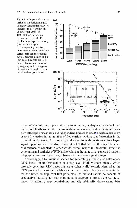
which rely largely on simple stationary assumptions, inadequate for analysis andprediction. Furthermore, the recombination process involved in creation of ran-dom telegraph noise is series of independent discrete events [5], where each eventcauses fluctuation in the number of free carriers leading to a fluctuation in thematerial conductance. Additionally, in the circuits with continuous-time large-signal operation and the discrete-event RTN that affects this operation arebi-directionally coupled; in other words, signal swings in the circuit affect thegeneration and statistics of RTN noise, while at the same time, generated randomtelegraph noise can trigger large changes to these very signal swings.
Accordingly, a technique is needed for generating genuinely non-stationaryRTN, based on uniformization of a trap-level Markov chain model, whichprovably generates RTN traces that are (stochastically) exactly identical to theRTN physically measured on fabricated circuits. While being a computationalmethod based on trap-level first principles, the method should be capable ofaccurately simulating non-stationary random telegraph noise at the circuit levelunder (i) arbitrary trap populations, and (ii) arbitrarily time-varying bias
90nm 65nm 45nm 32nm 22nm
CMOS technology
0
0.2
0.4
0.6
0.8
1.0
1.2Min VDD
Design margin
Local VTH
Global VTH
Static noise
RTNNBTI
No
n-i
dea
litie
s in
VD
D t
erm
s [V
]
(a)
100
101
102
103
104
105
frequency [Hz]
1/f2
10-24
10-23
10-22
10-21
10-20
10-19
SID
(f)
[A
2 /Hz]
ΔID/I D
[%
]
(c)
(b)
(d)0 2 4 6 8 10
time [ms]
0
1
2
-1
Fig. 6.1 a Impact of processvariation on design marginsof highly scaled circuits, RTNincrease from *10 mV in90 nm (year 2003) to150*200 mV in 22 nmtechnology (year 2011).b RTN power spectral density(Lorentizain shape).c Corresponding relativedrain current fluctuations, thecurrent through the channelswitch between a high and alow state. d Single RTN, abinary fluctuation is causedby trapping and de trappingof carrier at a single trap innear-interface gate oxide
6.2 Recommendations and Future Research 153
conditions. As such, solutions suitable for use in real circuit design situationsshould be provided, detailing how RTN affects circuit in the presence (as well asabsence) of other variability. Moreover, the method should be integrated withSPICE, without encountering efficiency issues, to conduct full-fledged RTNanalysis with varying trap populations under realistic, non-stationary operatingenvironments. An extensive study of CMOS scaling of low frequency noiseshould be provided, which will include consideration of high-j oxides, substratedoping, SiGe channels, and sizing effects in single and multi-gate devices in bothplanar and vertical 3D technology. Additionally, the extent to which randomtelegraph noise increases the probability of errors should be predicted quantita-tively and compared directly against measurements. Moreover, debuggingcapabilities and fault mechanism tracing capabilities should be provided, whichcan help explain and understand measurements, as well as devise and evaluatedesign/fabrication techniques for mitigating RTN generation and impact.
2. Tuning—Complex SOC with large die area require accurate workload monitorsas the unpredictability of a workload can lead to continuous power migration,and RTN can lead to parameter variability that can further conceal the workloadestimation accuracy. As a consequence, timely detection of workload migrationon a chip has become a challenging task, particularly as estimated values fromworkload monitors may be erroneous, noisy, or arrive too late to enableeffective application of power management mechanisms to avoid chip failure.Increasing the number of monitors could possible resolve this issue; never-theless the cost of adding a large number of monitors is prohibitive. Moreover,even without considering the cost of added monitors, other limitations such asadditional channels for routing and input/output may not allow placement ofmonitors near critical nodes required for accurate monitoring.
To be able to identify the effect of the defect activity on the operationparameters of the circuit, like the circuit’s delay or leakage energy, it is increas-ingly important to shift to a combined deterministic-stochastic view of reliabilityrelated phenomena. The deterministic quality refers to the model’s workloaddependency, which is based on the gate voltage dependent trap behavior (not juston the average duty cycle of the ones or zeros). The stochastic component mirrorsthe probabilistic nature of oxide defect activity. Moreover, that analysis can be thebasis of mitigation approaches based on workload tuning. The challenge that lies isto start searching for correlations between the imposed workload and its observedimpact on performance metrics. In that way, a more realistic view of the para-metric reliability in a realistic and detailed workload dependent way of largercircuits can be obtained. As a consequence, efficient and accurate unscented real-time workload tracking technique (for all chip locations) is required based on onlya few limited (noisy) monitor observations, which explicitly accounts for thenonlinear time-dependent circuit parameters. Adaptation mechanisms will need tobe defined, supported at the middle-ware level, which, together with applicationcomponents would enable various performance-reliability policies and tradeoffs.
154 6 Conclusions and Recommendations
In this way power management support could be provided as well as dependablecomputation enabled in the presence of random telegraph noise variations.
The goal of such task migration is to match the processing elements variationremoval capability to its workload and at the same time create a sufficient com-bination of high and low power tasks running on it. As each unit monitors only thelocal processing element and communicates with its nearest neighbors, suchframework will balance the workload and variation of the processors simulta-neously and potentially achieve significantly better scalability than the centralizedapproach. In that way, the rest of the system may be optimized for computations.
In such methodology, activity based dynamic voltage and frequency scaling(DVFS) (including well-bias monitoring devices, activity and process variationmonitors, DC/DC converter, temperature sensor and control loop) could be appliedto continuously track power/variability changes and threshold voltage hoppingcould be used to guardband variation safety. Additionally, such methodologycould include dynamic scaling of the frequency and voltage of the islands based onthe utilizations of the controlled queues. This online feedback control strategywould need to adjust the static voltage/frequency values in response to dynamicworkload variation. Run time support for adaptive mapping and scheduling(e.g. workload balancing, data and task migration, communication-dependentscheduling) would also need to be investigated such that variability conditions canbe supported on the designated computation platform. As a result, the architecturewould be tolerant to variations in HW availability (which can vary due to silicon,environmental and applications running conditions) and variations in applicationdemand, ranging from worst-case to marginal use). Similarly, the methodologywould need to contain a distributed online workload migration technique tosupport performance optimization and balance the layer instruction per cycledistribution to optimize instruction throughput, which could be integrated withinthe default (Linux) kernel workload balancing policy. The methodology couldbalance the power-variability budget assignment among processor cores in thesame layer. To that end, to minimize run-time overhead, iterative budgetingtechnique based on the switching activity (or IPC) will need to be developed.Similarly, the scheme could predict the impact of different workload combinationsand accordingly, adjusts the task allocation in a neighborhood providing pro-gressive improvement that reduces variation and prevents throttling events. Peri-odically, each core would adjust its voltage and frequency based on its assignedpower-variation budget. Upon a designated emergency, the routers at the emer-gency area would throttle incoming traffic in a distributed way, reducing powerconsumption in the region.
3. Circuit Utilization—In the deep-submicron regime, increasing leakage currentspreclude further constant field scaling. As a consequence the speed leverage ofnew technologies is moderate, especially in the field of low-power. Hence,without new architectural concepts (sub-) pico time-to-digital converters (TDC)resolution will not improve significantly in the future technology nodes. Thestatistical variation in circuit characteristics of CMOS circuitry caused by
6.2 Recommendations and Future Research 155
random telegraph noise could be utilized to obtain the effective fine timeresolution. This RTN-based time-to-digital converter may be highly nonlinear,but its nonlinearity can be compensated by the calibration method; in otherwords, the calibration makes the architecture practical for realizing a lineartime-to-digital converters with fine (sub-pico second) time-resolution. Since theRTN-based TDC utilizes the variation in characteristics positively, each MOStransistor in D flip-flops and delay line buffers would be implemented withminimum channel length and width leading to the reduced power consumption.
References
1. N. Tega, H. Miki, F. Pagette, D.J. Frank, A. Ray, M.J. Rooks, W. Haensch, K. Torii, Increasingthreshold voltage variation due to random telegraph noise in FETs as gate lengths scale to20 nm, in Proceedings of IEEE Symposium on VLSI Technology, 2009, 50–51
2. C.-H. Pao, M.-L. Fan, M.-F. Tsai, Y.-N. Chen, V.P.-H. Hu, P. Su, C.-T. Chuang, Impacts ofrandom telegraph noise on analog properties of FinFET and trigate devices and Widlar currentsource, in Proceedings of IEEE International Conference on IC Design and Technology, 2012,pp. 1–4
3. K. Ito, T. Matsumoto, S. Nishizawa, H. Sunagawa, Modeling of random telegraph noise undercircuit operation-simulation and measurement of RTN-induced delay fluctuation, in Proceed-ings of IEEE International Symposium on Quality Electronic Design, 2011, pp. 1–6
4. Y. Mori, K. Takeda, R. Yamada, Random telegraph noise of junction leakage current insubmicron devices. J. Appl. Phys. 107(1), 509–520 (2010)
5. T. Grasser, Stochastic charge trapping in oxides: from random telegraph noise to biastemperature instabilities. Microelectron. Reliab. 52(1), 39–70 (2012)
156 6 Conclusions and Recommendations
Appendix
A.1 MOS Transistor Model Uncertainty
The number of transistor process parameters that can vary is large. In previousresearch aimed at optimizing the yield of integrated circuits [1, 2], the number ofparameters simulated was reduced by choosing parameters which are relativelyindependent of each other, and which affect performance the most. The parametersmost frequently chosen are, for n and p-channel transistors: threshold voltage atzero back-bias for the reference transistor at the reference temperature VT0R, gainfactor for an infinite square transistor at the reference temperature bSQ, total lengthand width variation DLvar and DWvar, oxide thickness t0x, and bottom, sidewall andgate edge junction capacitance CJBR, CJSR and CJGR, respectively. The variation inabsolute value of all these parameters must be considered, as well as thedifferences between related elements, i.e. matching. The threshold voltagedifferences DVT and current factor differences Db are the dominant sourcesunderlying the drain-source current or gate-source voltage mismatch for a matchedpair of MOS transistors.
Transistor Threshold Voltage: Various factors affect the gate-source voltage atwhich the channel becomes conductive such as the voltage difference between thechannel and the substrate required for the channel to exist, the work functiondifference between the gate material and the substrate material, the voltage dropacross the thin oxide required for the depletion region, the voltage drop across thethin oxide due to implanted charge at the surface of the silicon, the voltage dropacross the thin oxide due to unavoidable charge trapped in the thin oxide, etc.
In order for the channel to exist the concentration of electron carriers in thechannel should be equal to the concentration of holes in the substrate, /S = -/F.The surface potential changed a total of 2/F between the strong inversion anddepletion cases. Threshold voltage is affected by the built-in Fermi potential due tothe different materials and doping concentrations used for the gate material and thesubstrate material. The work function difference is given by
/ms ¼ /F�Sub � /F�Gate ¼kT
qln
NDNA
n2i
ffi �ðA:1Þ
A. Zjajo, Stochastic Process Variation in Deep-Submicron CMOS, Springer Seriesin Advanced Microelectronics 48, DOI: 10.1007/978-94-007-7781-1,� Springer Science+Business Media Dordrecht 2014
157
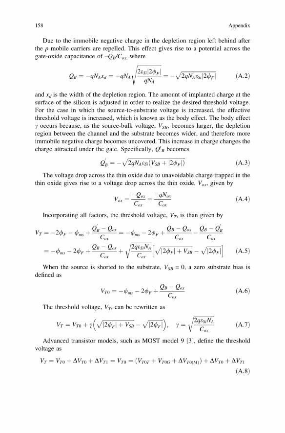
Due to the immobile negative charge in the depletion region left behind afterthe p mobile carriers are repelled. This effect gives rise to a potential across thegate-oxide capacitance of –QB/Cox, where
QB ¼ �qNAxd ¼ �qNA
ffiffiffiffiffiffiffiffiffiffiffiffiffiffiffiffiffiffi2eSi 2/Fj j
qNA
s
¼ �ffiffiffiffiffiffiffiffiffiffiffiffiffiffiffiffiffiffiffiffiffiffiffiffiffiffi2qNAeSi 2/Fj j
pðA:2Þ
and xd is the width of the depletion region. The amount of implanted charge at thesurface of the silicon is adjusted in order to realize the desired threshold voltage.For the case in which the source-to-substrate voltage is increased, the effectivethreshold voltage is increased, which is known as the body effect. The body effectc occurs because, as the source-bulk voltage, VSB, becomes larger, the depletionregion between the channel and the substrate becomes wider, and therefore moreimmobile negative charge becomes uncovered. This increase in charge changes thecharge attracted under the gate. Specifically, Q0B becomes
Q0
B ¼ �ffiffiffiffiffiffiffiffiffiffiffiffiffiffiffiffiffiffiffiffiffiffiffiffiffiffiffiffiffiffiffiffiffiffiffiffiffiffiffiffiffiffiffi2qNAeSi VSB þ 2/Fj jð Þ
pðA:3Þ
The voltage drop across the thin oxide due to unavoidable charge trapped in thethin oxide gives rise to a voltage drop across the thin oxide, Vox, given by
Vox ¼�Qox
Cox¼ �qNox
CoxðA:4Þ
Incorporating all factors, the threshold voltage, VT, is than given by
VT ¼ �2/F � /ms þQ0B � Qox
Cox¼ �/ms � 2/F þ
QB � Qox
Cox� QB � Q
0B
Cox
¼ �/ms � 2/F þQB � Qox
Coxþ
ffiffiffiffiffiffiffiffiffiffiffiffiffiffiffiffi2qeSiNA
Cox
r ffiffiffiffiffiffiffiffiffiffiffiffiffiffiffiffiffiffiffiffiffiffiffiffi2/Fj j þ VSB
p�
ffiffiffiffiffiffiffiffiffiffiffi2/Fj j
ph iðA:5Þ
When the source is shorted to the substrate, VSB = 0, a zero substrate bias isdefined as
VT0 ¼ �/ms � 2/F þQB � Qox
CoxðA:6Þ
The threshold voltage, VT, can be rewritten as
VT ¼ VT0 þ cffiffiffiffiffiffiffiffiffiffiffiffiffiffiffiffiffiffiffiffiffiffiffiffi2/Fj j þ VSB
p�
ffiffiffiffiffiffiffiffiffiffiffi2/Fj j
p� �; c ¼
ffiffiffiffiffiffiffiffiffiffiffiffiffiffiffiffi2qeSiNA
Cox
rðA:7Þ
Advanced transistor models, such as MOST model 9 [3], define the thresholdvoltage as
VT ¼ VT0 þ DVT0 þ DVT1 ¼ VT0 ¼ ðVT0T þ VT0G þ DVT0ðMÞÞ þ DVT0 þ DVT1
ðA:8Þ
158 Appendix

where threshold voltage at zero back-bias VT0 [V] for the actual transistor at theactual temperature is defined as geometrical model, VT0T [V] is thresholdtemperature dependence, VT0G [V] threshold geometrical dependence and DVT0(M)
[V] matching deviation of threshold voltage. Due to the variation in the doping inthe depletion region under the gate, a two-factor body-effect model is needed toaccount for the increase in threshold voltage with VSB for ion-implantedtransistors. The change in threshold voltage for non-zero back bias isrepresented in the model as
DVT0 ¼
K0 uS � uS0ð Þ uS� uSX
1� KK0
� �2� �
K0uSX � K0uS0
þK
ffiffiffiffiffiffiffiffiffiffiffiffiffiffiffiffiffiffiffiffiffiffiffiffiffiffiffiffiffiffiffiffiffiffiffiffiffiffiffiffiffiffi
u2S � 1� K
K0
� �2� �
u2SX
s
uS� uSX
8>>>>><
>>>>>:
ðA:9Þ
uS ¼ffiffiffiffiffiffiffiffiffiffiffiffiffiffiffiffiffiffiffiVSB þ /B
puS0 ¼
ffiffiffiffiffiffi/B
puST ¼
ffiffiffiffiffiffiffiffiffiffiffiffiffiffiffiffiffiffiffiffiffiVSBT þ /B
puSX ¼
ffiffiffiffiffiffiffiffiffiffiffiffiffiffiffiffiffiffiffiffiffiVSBX þ /B
p
ðA:10Þ
where the parameter VSBX [V] is the back-bias value, at which the implementedlayer becomes fully depleted, K0 [V1/2] is low-backbias body factor for the actualtransistor and K [V1/2] is high-backbias body factor for the actual transistor. Fornon-zero values of the drain bias, the drain depletion layer expands towards thesource and may affect the potential barrier between the source and channel regionsespecially for short-channel devices. This modulation of the potential barrierbetween source and channel causes a reduction in the threshold voltage.In subthreshold this dramatically increases the current and is referred to as draininduced barrier lowering (DIBL). Once an inversion layer has been formed athigher values of gate bias, any increase of drain bias induces an additional increasein inversion charge at the drain end of the channel. The drain bias still has a smalleffect in the threshold voltage and this effect is most pronounced in the outputconductance in strong inversion and is referred to as static feedback. The DIBLeffect is modeled by the parameter c00 in the subthreshold region. This drain biasvoltage dependence is expressed by first part of
DVT1 ¼ �c0V2
GTX
V2GTX þ V2
GT1
VDS � c1V2
GT1
V2GTX þ V2
GT1
VgDSDS ðA:11Þ
VGT1 ¼VGS � VT1 VGS�VT1
0 VGS�VT1
VGTX ¼
ffiffiffi2p
=2 ðA:12Þ
where c1 is coefficient for the drain induced threshold shift for large gate drive forthe actual transistor and gDS exponent of the VDS dependence of c1 for the actualtransistor. The static feedback effect is modeled by c1. This can be interpreted asanother change of effective gate drive and is modeled by the second part of (A.9).
Appendix 159
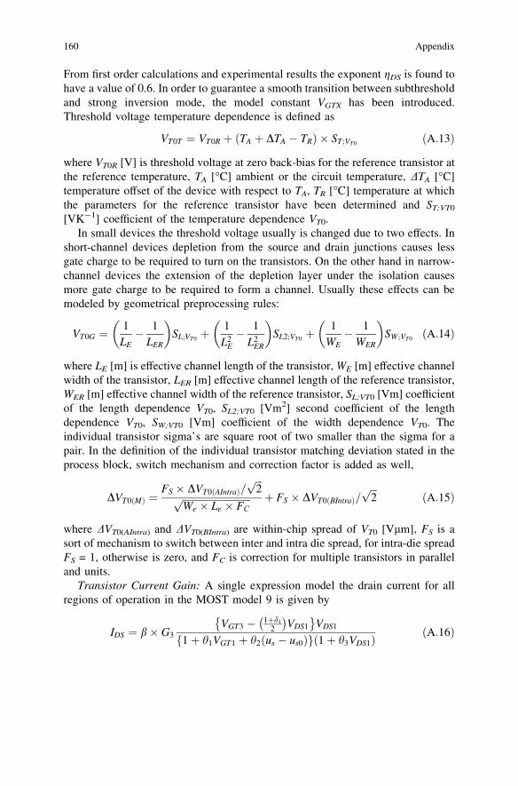
From first order calculations and experimental results the exponent gDS is found tohave a value of 0.6. In order to guarantee a smooth transition between subthresholdand strong inversion mode, the model constant VGTX has been introduced.Threshold voltage temperature dependence is defined as
VT0T ¼ VT0R þ TA þ DTA � TRð Þ � ST ;VT0 ðA:13Þ
where VT0R [V] is threshold voltage at zero back-bias for the reference transistor atthe reference temperature, TA [�C] ambient or the circuit temperature, DTA [�C]temperature offset of the device with respect to TA, TR [�C] temperature at whichthe parameters for the reference transistor have been determined and ST;VT0
[VK-1] coefficient of the temperature dependence VT0.In small devices the threshold voltage usually is changed due to two effects. In
short-channel devices depletion from the source and drain junctions causes lessgate charge to be required to turn on the transistors. On the other hand in narrow-channel devices the extension of the depletion layer under the isolation causesmore gate charge to be required to form a channel. Usually these effects can bemodeled by geometrical preprocessing rules:
VT0G ¼1
LE� 1
LER
ffi �SL;VT0 þ
1L2
E
� 1L2
ER
ffi �SL2;VT0 þ
1WE� 1
WER
ffi �SW;VT0 ðA:14Þ
where LE [m] is effective channel length of the transistor, WE [m] effective channelwidth of the transistor, LER [m] effective channel length of the reference transistor,WER [m] effective channel width of the reference transistor, SL;VT0 [Vm] coefficientof the length dependence VT0, SL2;VT0 [Vm2] second coefficient of the lengthdependence VT0, SW;VT0 [Vm] coefficient of the width dependence VT0. Theindividual transistor sigma’s are square root of two smaller than the sigma for apair. In the definition of the individual transistor matching deviation stated in theprocess block, switch mechanism and correction factor is added as well,
DVT0ðMÞ ¼FS � DVT0ðAIntraÞ=
ffiffiffi2p
ffiffiffiffiffiffiffiffiffiffiffiffiffiffiffiffiffiffiffiffiffiffiffiffiffiffiffiffiWe � Le � FCp þ FS � DVT0ðBIntraÞ=
ffiffiffi2p
ðA:15Þ
where DVT0(AIntra) and DVT0(BIntra) are within-chip spread of VT0 [Vlm], FS is asort of mechanism to switch between inter and intra die spread, for intra-die spreadFS = 1, otherwise is zero, and FC is correction for multiple transistors in paralleland units.
Transistor Current Gain: A single expression model the drain current for allregions of operation in the MOST model 9 is given by
IDS ¼ b� G3VGT3 � 1þd1
2
�VDS1
� VDS1
1þ h1VGT1 þ h2 us � us0ð Þf g 1þ h3VDS1ð Þ ðA:16Þ
160 Appendix
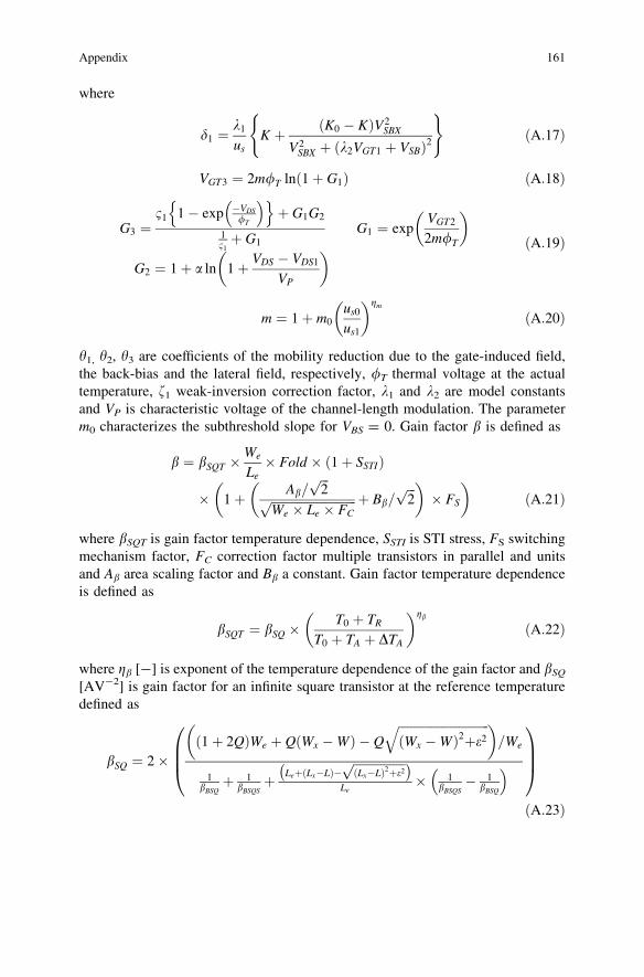
where
d1 ¼k1
usK þ K0 � Kð ÞV2
SBX
V2SBX þ k2VGT1 þ VSBð Þ2
( )ðA:17Þ
VGT3 ¼ 2m/T ln 1þ G1ð Þ ðA:18Þ
G3 ¼11 1� exp �VDS
/T
� �n oþ G1G2
111þ G1
G1 ¼ expVGT2
2m/T
ffi �
G2 ¼ 1þ a ln 1þ VDS � VDS1
VP
ffi � ðA:19Þ
m ¼ 1þ m0us0
us1
ffi �gm
ðA:20Þ
h1, h2, h3 are coefficients of the mobility reduction due to the gate-induced field,the back-bias and the lateral field, respectively, /T thermal voltage at the actualtemperature, f1 weak-inversion correction factor, k1 and k2 are model constantsand VP is characteristic voltage of the channel-length modulation. The parameterm0 characterizes the subthreshold slope for VBS = 0. Gain factor b is defined as
b ¼ bSQT �We
Le� Fold � 1þ SSTIð Þ
� 1þ Ab=ffiffiffi2p
ffiffiffiffiffiffiffiffiffiffiffiffiffiffiffiffiffiffiffiffiffiffiffiffiffiffiffiffiWe � Le � FCp þ Bb=
ffiffiffi2pffi �
� FS
ffi �ðA:21Þ
where bSQT is gain factor temperature dependence, SSTI is STI stress, FS switchingmechanism factor, FC correction factor multiple transistors in parallel and unitsand Ab area scaling factor and Bb a constant. Gain factor temperature dependenceis defined as
bSQT ¼ bSQ �T0 þ TR
T0 þ TA þ DTA
ffi �gb
ðA:22Þ
where gb [-] is exponent of the temperature dependence of the gain factor and bSQ
[AV-2] is gain factor for an infinite square transistor at the reference temperaturedefined as
bSQ ¼ 2�1þ 2Qð ÞWe þ Q Wx �Wð Þ � Q
ffiffiffiffiffiffiffiffiffiffiffiffiffiffiffiffiffiffiffiffiffiffiffiffiffiffiffiffiffiffiWx �Wð Þ2þe2
qffi �=We
1bBSQþ 1
bBSQSþ Leþ Lx�Lð Þ�
ffiffiffiffiffiffiffiffiffiffiffiffiffiffiffiffiffiLx�Lð Þ2þe2
p �
Le� 1
bBSQS� 1
bBSQ
� �
0BB@
1CCA
ðA:23Þ
Appendix 161

bBSQ ¼ bSQTR �T0 þ TR
T0 þ TA þ DTA
ffi �gbBSQ
bBSQS ¼ bSQSTR �T0 þ TR
T0 þ TA þ DTA
ffi �gbBSQSðA:24Þ
For devices in the ohmic region (A.24) can be approximated by
ID ffi bVGS � VT � 1
2 VDS
1þ h VGS � VTð Þ VDS ðA:25Þ
and for saturated devices
ID ffib2
VGS � VTð Þ2
1þ h VGS � VTð Þ ðA:26Þ
Change in drain current can be calculated by
DID ¼ DboID
ob
� �þ DVT
oID
oVT
� �þ Dh
oID
oh
� �ðA:27Þ
leading to drain current mismatch
DID
IDffi Db
b� ixDVT � nxDh ðA:28Þ
where for ohmic
io ¼1þ 1
2 hVDS
VGS � VT � 12 VDS
�1þ h VGS � VTð Þð Þ
no ¼VGS � VTð Þ
1þ h VGS � VTð ÞDh ðA:29Þ
and for saturation
is ¼2þ h VGS � VTð Þ
VGS � VTð Þ 1þ h VGS � VTð Þð Þ ns ¼VGS � VTð Þ
1þ h VGS � VTð ÞDh ðA:30Þ
The standard deviation of the mismatch parameters is derived by
r2 DID
ID
ffi �¼r2 Db
b
ffi �þ i2
xr2 DVTð Þ þ n2
xr2 Dhð Þ
þ 2qDbb;DVT
ffi �ixr DVTð Þr Db
b
ffi �þ 2q
Dbb;Dh
ffi �nxr Dhð Þr Db
b
ffi �
þ 2q DVT ;Dhð Þixnxr Dhð Þr DVð Þ ðA:31Þ
with [4]
rðDVTÞ ¼AVT=
ffiffiffi2p
ffiffiffiffiffiffiffiffiffiffiffiffiffiffiffiWeff Leff
p þ BVT=ffiffiffi2pþ SVT D ðA:32Þ
162 Appendix

rDbb
ffi �¼ Ab=
ffiffiffi2p
ffiffiffiffiffiffiffiffiffiffiffiffiffiffiffiWeff Leff
p þ Bb=ffiffiffi2pþ SbD ðA:33Þ
where Weff is the effective gate-width and Leff the effective gate-length, theproportionality constants AVT, SVT, Ab and Sb are technology-dependent factors,D is distance and BVT and Bb are constants. For widely spaced devices termsSVTD and SbD are included in the models for the random variations in two previousequations, but for typical device separations (\1 mm) and typical device sizes thiscorrection is small. Most mismatch characterization has been performed ondevices in strong inversion, in the saturation or linear region but some studies fordevices operating in weak inversion have also been conducted. Qualitatively, thebehavior in all regions is very similar; VT and b variations are the dominant sourceof mismatch and their matching scales with device area. The effective mobilitydegradation mismatch term can be combined with the current factor mismatchterm, as both terms become significant in the same bias range (high gate voltage).The correlation factor q(DVT, Db/b) can be ignored as well, since correlationbetween r(DVT) and the other mismatch parameters remains low for both smalland large devices. The drain source current error DID/ID is important for thevoltage biased pair. For the current biased pair, the gate-source or input referredmismatch should be considered, whose expression could be derived similarly asfor drain source current error. Change in gate-source voltage can be calculated by
DVGS ¼ DVToVGS
oVT
� �þ Db
oVGS
ob
� �ðA:34Þ
leading to the standard deviation of the mismatch parameters is derived by
r2 DVGS
VGS
ffi �¼ r2 DVTð Þ þ #2r2 Db
b
ffi �where # ¼ VGS � VTð Þ
2ðA:35Þ
MOS transistor current matching or gate-source matching is bias pointdependent, and for typical bias points, VT mismatch is the dominant error sourcefor drain-source current or gate-source voltage matching.
Transistor width W and length L: The electrical transistor length is determinedby the combination of physical polysilicon track width, spacer processing, mask-,projection- and etch- variations
Le ¼ Lþ DLvar ¼ Lþ DLPS � 2� DLoverlap ðA:36Þ
where Le is effective electrical transistor channel length, determined by linearregion MOS transistor measurements on several transistors with varying length,L drawn width of the polysilicon gate, DLvar total length variation, DLPS lengthvariation due to mask, projection, lithographic, etch, etc. variations and DLoverlap
effective source/gate or drain/gate overlap per side due to lateral diffusion. Theelectrical transistor width is determined by the combination of physical activeregion width, mask, projection and etch variations
Appendix 163
We ¼ W þ DWvar ¼ W þ DWOD � 2� DWnarrow ðA:37Þ
where We is effective electrical transistor channel width, determined by linearregion MOS transistor measurements on several transistors with varying width,W drawn width of the active region, DWvar total width variation, DWOD widthvariations due to mask, projection, lithographic, etch, etc. variations and DWnarrow
diffusion width offset: effective diffusion width increase due to lateral diffusion ofthe n+ or p+ implementation.
Oxide thickness: The modeling of oxide thickness tox has impact on: totalcapacitance from the gate to the ground: Cox = eox(We Le)/tox, gain factor: b—gainfactor, SL;h1R—coefficient of the length dependence of h1, h1R—coefficient of themobility reduction due to the gate-induced field, subtreshold behaviour: m0R—factor of the subthreshold slope for the reference transistor at the referencetemperature, overlap capacitances: CGD0 = WE 9 Col = WE 9 (eox LD)/tox, andCGS0 = CGD0, and bulk factors: K0R—low-backbias body factor and KR—high-backbias body factor.
Junction capacitances: The depletion-region capacitance is nonlinear and isformed by: n+–p-: n-channel source/drain to p-substrate junction, p+–n-: p-channel source/drain to n-well junction and n-–p-: n-well to p-substrate junction.Depletion capacitance of a pn or np junction consists of bottom, sidewall and gateedge component. Capacitance of bottom area AB is given as
CJB ¼ CJBR � ABVDBR � VR
VDB
ffi �PB
ðA:38Þ
where AB [m2] is diffusion area, VR [V] voltage at which parameters have beendetermined, VDB [V] diffusion voltage of bottom area AB, VDBR [V] diffusionvoltage of the bottom junction at T = TR and PB [-] bottom-junction gradingcoefficient.
Similar formulations hold for the locos-edge and the gate-edge components;one has to replace the index B by S and G, and the area AB by LS and LG.Capacitance of the bottom component is derived as
CJBV ¼
CJBR
1� VVDB
� �PBV\VLB
CLB þ CLB�PB V�VLBð ÞVDB 1�FCBð Þ V �VLB
8><
>:ðA:39Þ
where
CLB ¼ CJB 1� FCBð ÞPB FCB ¼ 1� 1þ PB
3
ffi � 1PB
VLB ¼ FCB � VDB ðA:40Þ
164 Appendix
and V is diode bias voltage. Similar expressions can be derived for sidewall CJSV
and gate edge component CJGV. The total diode depletion capacitance can bedescribed by:
C ¼ CJBV þ CJSV þ CJGV ðA:41Þ
A.2 Resistor and Capacitor Model Uncertainty
Typical CMOS and BiCMOS technologies offer several different resistors, such asdiffusion nþ=pþ resistors, nþ=pþ poly resistors, and nwell resistor. Many factorsin the fabrication of a resistor such as the fluctuations of the film thickness, dopingconcentration, doping profile, and the dimension variation caused by thephotolithographic inaccuracies and non-uniform etch rates can displaysignificant variation in the sheet resistance. However, this is bearable as long asthe device matching properties are within the range the designs require. Thefluctuations of the resistance of the resistor can be categorized into two groups, onefor which the fluctuations occurring in the whole device are scaled with the devicearea, called area fluctuations, another on in which fluctuations takes place onlyalong the edges of the device and therefore scaled with the periphery, calledperipheral fluctuations. For a matched resistor pair with width W and resistance R,the standard deviation of the random mismatch between the resistors is
r ¼ffiffiffiffiffiffiffiffiffiffiffiffiffiffifa þ
fpW
r ,W
ffiffiffiRp� �
ðA:42Þ
where fa and fp are constants describing the contributions of area and peripheryfluctuations, respectively. In circuit applications, to achieve required matching,resistors with width (at least 2–3 times) wider than minimum width should beused. Also, resistors with higher resistance (longer length) at fixed width exhibitlarger mismatching. To achieve the desired matching, it has been a commonpractice that a resistor with long length (for high resistance) is broken into shorterresistors in series. To model a (poly-silicon) resistor following equation is used
R ¼ RshL
W þ DWþ Re
W þ DWðA:43Þ
where Rsh is the sheet resistance of the poly resistor, Re is the end resistancecoefficient, W and L are resistor width and length, DW is the resistor width offset.The correlations between standard deviations (r) of the model parameters and thestandard deviation of the resistance are given in the following
r2R ¼ r2
Rsh
dR
dRsh
� �2
þr2Re
dR
dRe
� �2
þr2DW
dR
dDW
� �2
ðA:44Þ
Appendix 165
r2R ¼ r2
Rsh
L2
W þ DWð Þ2þ r2
Re
1
W þ DWð Þ2þ r2
DW
L� Rsh
W þ DWð Þ2þ Re
W þ DWð Þ2
" #2
ðA:45Þ
To define the resistor matching,
r2DRR¼ r2
Rsh
L
L� Rsh þ Reð Þ
� �2
þr2Re
1L� Rsh þ Reð Þ
� �2
þr2DW
1
W þ DWð Þ2
" #2
ðA:46Þ
rRsh ¼ ARshffiffiffiffiffiWLp rRe ¼ ARe rDW ¼ ADW
W1ffiffi2p ðA:47Þ
Current CMOS technology provides various capacitance options, such as poly-to-poly capacitors, metal-to-metal capacitors, MOS capacitors, and junctioncapacitors. The integrated capacitors show significant variability due to the processvariation. For a MOS capacitor, the capacitance values are strongly dependent onthe change in oxide thickness and doping profile in the channel besides thevariation in geometries.
Similar to the resistors the matching behavior of capacitors depends on therandom mismatch due to periphery and area fluctuations with a standard deviation
r ¼ffiffiffiffiffiffiffiffiffiffiffiffiffifa þ
fpC
r ,ffiffiffiffiCp
ðA:48Þ
where fa and fp are factors describing the influence of the area and peripheryfluctuations, respectively. The contribution of the periphery components decreasesas the area (capacitance) increases. For very large capacitors, the area componentsdominate and the random mismatch becomes inversely proportional to
ffiffiffiffiCp
.A simple capacitor mismatch model is given by
r2DCC¼ r2
p þ r2a þ r2
d rp ¼ fp
C34
ra ¼ fa
C12
rd ¼ fd � d ðA:49Þ
where fp, fa and fd are constants describing the influence of periphery, area, anddistance fluctuations. The periphery component models the effect of edgeroughness, and it is most significant for small capacitors, which have relativelylarge amount of edge capacitance. The area component models the effect of short-range dielectric thickness variations, and it is most significant for moderate sizecapacitors. The distance component models the effect of global dielectric thicknessvariations across the wafer, and it becomes significant for large capacitors orwidely spaced capacitors.
166 Appendix
A.3 Time-Domain Analysis
The modern analog circuit simulators use a modified form of nodal analysis [5, 6]and Newton-Raphson iteration to solve the system of n non-linear equations fi inn variables pi. In general, the time-dependent behavior of a circuit containinglinear or nonlinear elements may be described as [7]
q0 � Ev ¼ 0 q0 ¼ qð0Þf ðq; v;w; p; tÞ ¼ 0
ðA:50Þ
This notation assumes that the terminal equations for capacitors and inductorsare defined in terms of charges and fluxes, collected in q. The elements of matrixE are either 1 or 0, and v represents the circuit variables (nodal voltages or branchcurrents). All non linearity’s are incorporated in the algebraic system f(q, v, w, p,t) = 0, so the differential equations q0-Ev = 0 are linear. The initial conditionsare represented by q0. Furthermore, w is a vector of excitations, and p contains thecircuit parameters like parameters of linear or non linear components. An elementof p may also be a (non linear) function of the circuit parameters. It is assumedthat for each p there is only one solution of v. The dc solution is computed bysolving the system
�Ev0 ¼ 0
f ðq0; v0;w0; pi; 0Þ ¼ 0ðA:51Þ
which is derived by setting q0 = 0. The solution (q0, v0) is fond by Newton-Raphson iteration. In general, this technique finds the solution of a nonlinearsystem F(v) = 0 by iteratively solving the Newton-Raphson equation
JkDvk ¼ �f ðvkÞ ðA:52Þ
where Jk is the Jacobian of f, with (Jk)ij = qfi/qvjk. Iteration starts with estimatev0.
After Dvk is computed in the kth iteration, vk + 1 is found as vk + 1 = vk + Dvk andthe next iteration stars. The iteration terminates when Dvk is sufficiently small. Forthe (A.51), the Newton-Raphson equation is
0 �Eofoq0
ofov0
� �Dq0
Dv0
� �¼ � �Ev
f
� �ðA:53Þ
which is solved by iteration (for simplicity it is assumed that the excitations w donot depend on pj). This scheme is used in the dc operating point [5–7], dc transfercurve, and even time-domain analysis; in the last case, the dependence upon timeis eliminated by approximating the differential equations by difference equations[7]. Only frequency-domain (small signal) analyses are significantly differentbecause they require (for each frequency) a solution of a system of simultaneouslinear equations in the complex domain; this is often done by separating the realand imaginary parts of coefficients and variables, and solving a twice as largesystem of linear equations in the real domain.
Appendix 167

The main computational effort of numerical circuit simulation in typicalapplications is thus devoted to: (i) evaluating the Jacobian J and the function f, andthen (ii) solving the system of linear equations. After the dc solution (q0, v0) isobtained, the dc derivatives are computed. Differentiation of (A.51) with respect topj results in linear system
0 �Eofoq0
ofov0
� � oq0opj
ov0opj
" #¼ �
0� of
opj
� �ðA:54Þ
The (A.51) can be solved efficiently by using the LU factorization [8] of theJacobian that was computed at the last iteration of (A.53). Now the derivatives of(A.50) to pj is computed. Differentiation of (A.50) to pj results in linear, time-varying system
oq0
opj� E ov
opj¼ 0 oq0
opj¼ oqð0Þ
opj
of
oq
oq
opjþ of
ovovopjþ of
opj¼ 0
ðA:55Þ
At each time point the circuit derivatives are obtained by solving previoussystem of equation after the original system is solved. Suppose, for example, that akth order Backward Differentiation Formula (BDF) is used [9, 10], with thecorrector
ðq0Þnþk ¼ � 1Dt
Xk�1
i¼0
aiqnþk�i ðA:56Þ
where the coefficients ai depend upon the order k of the BDF formula. Aftersubstituting (A.56) into (A.50), the Newton-Raphson equation is derived as
� a0Dt �E
ofoq
ofov
" #Dqnþk
Dvnþk
� �¼ � � 1
Dt
Pk�1
t¼0aiqnþk�i�Evnþk
f ðqnþk; vnþk;wnþk; pj; tnþkÞ
2
4
3
5 ðA:57Þ
Iteration on this system provides the solution (qn + k, vn + k). Substituiting a kthorder BDF formula in (A.55) gives the linear system
� a0Dt �E
ofoq
ofot
" # oqopj
� �
nþk
otopj
� �
nþk
264
375 ¼
� 1Dt
Pk�1
t¼0ai
oqopj
� �
nþk�i
� ofopj
264
375 ðA:58Þ
Thus (A.57) and (A.58) have the same system matrix. The LU factorization ofthis matrix is available after (A.57) is iteratively solved. Then a forward andbackward substitution solves (A.58). For each parameter the right-hand side of(A.58) is different and the forward and backward substitution must be repeated.
168 Appendix
If random term N(p, t)�g, which models the tolerance effects is non-zero andadded to the equation (A.50) [11–15]
f ðq; v;w; p; tÞ þ Nðp; tÞ � g ¼ 0 ðA:59Þ
Solving this system means to determine the probability density function of therandom vector p(t) at each time instant t. For two instants in time, t1 and t2, withDt = t1t0 and Dt2 = t2-t0 where t0 is a time that coincides with dc solution ofcircuit performance function v, Dt is assumed to satisfy the criteria that circuitperformance function v can be designated as the quasi-static. To make the problemmanageable, the function can be linearized by first-order Taylor approximationassuming that the magnitude of the random term p is sufficiently small to considerthe equation as linear in the range of variability of p or the nonlinearites are sosmooth that they might be considered as linear even for a wide range of p asexplained in Sect. 2.2.
A.4 Parameter Extraction
Once the nominal parameter vector p0 is found for the nominal device, theparameter extraction of all device parameters pk of the transistors connected toparticular node n can be performed using a linear approximation to the model. Letp = [p1, p2,…,pn]T[Rn denote the parameter vector, f = [f1, f2,…,fm]T[Rm
performance vector, zk = [z1k, z2
k,…,zmk]T[Rm the measured performance vector
of the kth device and w a vector of excitations w = [w1, w2,…,wl]T[ Rl.
Considering equation (A.50)
q0 � Ev ¼ 0 q0 ¼ qð0Þ
f ðq; v;w; p; tÞ ¼ 0ðA:60Þ
general model can be written. The measurements can only be made under certainselected values of w, and if the initial conditions q0 are met, so the model can besimply denoted as
f ðpÞ ¼ 0 ðA:61Þ
To extract a parameter vector pk corresponding to the kth device
pk ¼ arg minpk2Rn
f ðpkÞ � zk�� ��
�ðA:62Þ
is found. The weighted sum of error squares for the kth device is formed as [7]
eðpkÞ ¼ 12
Xm
i¼1
wi½fiðpkÞ � zki �
2 ¼ 12½f ðpkÞ � zk�T W ½f ðpkÞ � zk� ðA:63Þ
Appendix 169
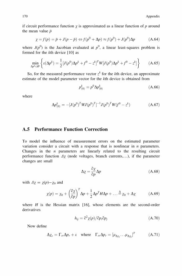
if circuit performance function v is approximated as a linear function of p aroundthe mean value �p
v ¼ f ðpÞ ¼ �pþ Jðp� �pÞ , f ðp0 þ DpÞ f ðp0Þ þ Jðp0ÞDp ðA:64Þ
where J(p0) is the Jacobian evaluated at p0, a linear least-squares problem isformed for the kth device [10] as
minDpk2Rn
eðDpkÞ ¼ 12½Jðp0ÞDpk þ f 0 � zk�T W ½Jðp0ÞDpk þ f 0 � zk�
�ðA:65Þ
So, for the measured performance vector zk for the kth device, an approximateestimate of the model parameter vector for the kth device is obtained from
pkð0Þ ¼ p0Dpk
ð0Þ ðA:66Þ
where
Dpkð0Þ ¼ �½Jðp0ÞT WJðp0ÞT ��1Jðp0ÞT Wðf 0 � zkÞ ðA:67Þ
A.5 Performance Function Correction
To model the influence of measurement errors on the estimated parametervariation consider a circuit with a response that is nonlinear in n parameters.Changes in the n parameters are linearly related to the resulting circuitperformance function Dv (node voltages, branch currents,…), if the parameterchanges are small
Dv ¼ ovop
Dp ðA:68Þ
with Dv = v(p)-v0 and
vðpÞ ¼ v0 þovop
ffi �T
Dpþ 12
DpT HDpþ . . .¼D v0 þ Dv ðA:69Þ
where H is the Hessian matrix [16], whose elements are the second-orderderivatives
hij ¼ o2vðpÞ=opiopj ðA:70Þ
Now define
Dvr ¼ CrrDpr þ e where CrrDpr ¼ ½lDv1. . .lDvk
�T ðA:71Þ
170 Appendix
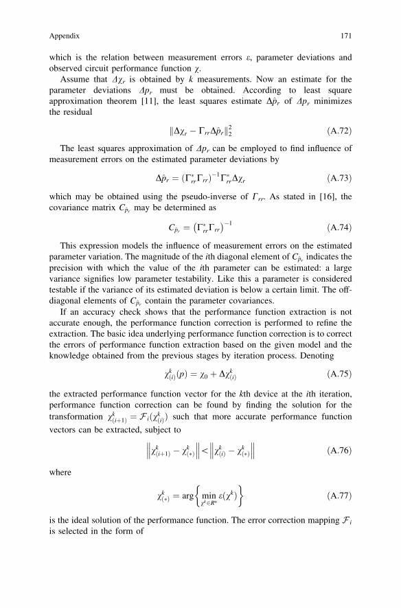
which is the relation between measurement errors e, parameter deviations andobserved circuit performance function v.
Assume that Dvr is obtained by k measurements. Now an estimate for theparameter deviations Dpr must be obtained. According to least squareapproximation theorem [11], the least squares estimate Dpr of Dpr minimizesthe residual
Dvr � CrrDprk k22 ðA:72Þ
The least squares approximation of Dpr can be employed to find influence ofmeasurement errors on the estimated parameter deviations by
Dpr ¼ ðCrrCrrÞ�1CrrDvr ðA:73Þ
which may be obtained using the pseudo-inverse of Crr. As stated in [16], thecovariance matrix Cpr may be determined as
Cpr ¼ CrrCrr
��1 ðA:74Þ
This expression models the influence of measurement errors on the estimatedparameter variation. The magnitude of the ith diagonal element of Cpr indicates theprecision with which the value of the ith parameter can be estimated: a largevariance signifies low parameter testability. Like this a parameter is consideredtestable if the variance of its estimated deviation is below a certain limit. The off-diagonal elements of Cpr contain the parameter covariances.
If an accuracy check shows that the performance function extraction is notaccurate enough, the performance function correction is performed to refine theextraction. The basic idea underlying performance function correction is to correctthe errors of performance function extraction based on the given model and theknowledge obtained from the previous stages by iteration process. Denoting
vkðiÞðpÞ ¼ v0 þ Dvk
ðiÞ ðA:75Þ
the extracted performance function vector for the kth device at the ith iteration,performance function correction can be found by finding the solution for thetransformation vk
ðiþ1Þ ¼ F iðvkið ÞÞ such that more accurate performance function
vectors can be extracted, subject to
vkðiþ1Þ � vk
ðÞ
������\ vk
ðiÞ � vkðÞ
������ ðA:76Þ
where
vkðÞ ¼ arg min
vk2RneðvkÞ
�ðA:77Þ
is the ideal solution of the performance function. The error correction mapping F i
is selected in the form of
Appendix 171
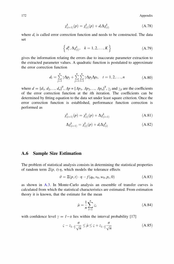
vkðiþ1ÞðpÞ ¼ vk
ðiÞðpÞ þ diDvkðiÞ ðA:78Þ
where di is called error correction function and needs to be constructed. The dataset
dki ;Dvk
ðiÞ; k ¼ 1; 2; . . .;Kn o
ðA:79Þ
gives the information relating the errors due to inaccurate parameter extraction tothe extracted parameter values. A quadratic function is postulated to approximatethe error correction function
dt ¼Pn
j¼1cDpj þ
Pn
j¼1
Pn
l¼1cDpjDpl; t ¼ 1; 2; . . .; n ðA:80Þ
where d = [d1, d2,…, dn]T, Dp = [Dp1, Dp2,…, Dpn]T, cj and cjl are the coefficientsof the error correction function at the ith iteration. The coefficients can bedetermined by fitting equation to the data set under least square criterion. Once theerror correction function is established, performance function correction isperformed as
vkðiþ1ÞðpÞ ¼ vk
ðiÞðpÞ þ Dvkðiþ1Þ ðA:81Þ
Dvkðiþ1Þ ¼ vk
ðiÞðpÞ þ diDvkðiÞ ðA:82Þ
A.6 Sample Size Estimation
The problem of statistical analysis consists in determining the statistical propertiesof random term N(p, t)�g, which models the tolerance effects
# ¼ Nðp; tÞ � g� f ðq0; t0;w0; pi; 0Þ ðA:83Þ
as shown in A.3. In Monte-Carlo analysis an ensemble of transfer curves iscalculated from which the statistical characteristics are estimated. From estimationtheory it is known, that the estimate for the mean
l ¼ 1n
Xn
i¼1
1i ðA:84Þ
with confidence level c = 1-a lies within the interval probability [17]
1� z1�d2
rffiffiffinp � l� 1þ z1�d
2
rffiffiffinp ðA:85Þ
172 Appendix
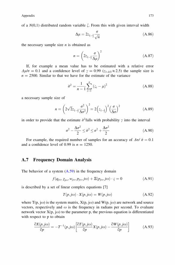
of a N(0,1) distributed random variable f. From this with given interval width
Dl ¼ 2z1�d2
rffiffiffinp ðA:86Þ
the necessary sample size n is obtained as
n ¼ 2z1�d2
rDl
ffi �2
ðA:87Þ
If, for example a mean value has to be estimated with a relative errorDl/r = 0.1 and a confidence level of c = 0.99 (z1-d/2&2.5) the sample size isn = 2500. Similar to that we have for the estimate of the variance
r2 ¼ 1n� 1
Xn
i¼1
ð1i � lÞ2 ðA:88Þ
a necessary sample size of
n ¼ 2ffiffiffi2p
z1�d2
r2
Dr2
ffi �2
¼ 2 z1�d2
� �2 rDr
� �2ðA:89Þ
in order to provide that the estimate r2falls with probability c into the interval
r2 � Dr2
2� r2� r2 þ Dr2
2ðA:90Þ
For example, the required number of samples for an accuracy of Dr/ r ¼ 0:1and a confidence level of 0.99 is n = 1250.
A.7 Frequency Domain Analysis
The behavior of a system (A.59) in the frequency domain
f ðqjx; vjx;wjx; pjx; jxÞ þ Nðpjx; jxÞ � 1 ¼ 0 ðA:91Þ
is described by a set of linear complex equations [7]
Tðp; jxÞ � Xðp; jxÞ ¼ Wðp; jxÞ ðA:92Þ
where T(p, jx) is the system matrix, X(p, jx) and W(p, jx) are network and sourcevectors, respectively and x is the frequency in radians per second. To evaluatenetwork vector X(p, jx) to the parameter p, the previous equation is differentiatedwith respect to p to obtain
oXðp; jxÞop
¼ �T�1ðp; jxÞ oTðp; jxÞop
Xðp; jxÞ � oWðp; jxÞop
� �ðA:93Þ
Appendix 173
The circuit performance function v = f(p,jx) is obtained from v = f(p,jx) = dTX(p, jx) using the adjoint or transpose method [18] where the vector dis a constant vector that specifies the circuit performance function. The derivativesof the circuit performance function with respect to VT and b are then computedfrom
ovðVTi; jxÞoVTi
¼ �dT T�1ðVTi; jxÞoTðVTi; jxÞ
oVTiXðVTi; jxÞ �
oWðVTi; jxÞoVTi
� �ðA:94Þ
ovðbi; jxÞobi
¼ �dT T�1ðbi; jxÞoTðbi; jxÞ
obiXðbi; jxÞ �
oWðbi; jxÞobi
� �ðA:95Þ
The first order derivatives of the magnitude of the circuit performance functionare computed from
o vðjxÞj joVTi
¼ vðVTi; jxÞj jRe1
vðVTi; jxÞovðVTi; jxÞ
oVTi
� �ðA:96Þ
o vðbi; jxÞj jobi
¼ o vðbi; jxÞj jRe1
vðbi; jxÞovðbi; jxÞ
obi
� �ðA:97Þ
where ‘Re’ denotes the real part of the complex variable function. The secondorder derivatives are calculated from
o2 vðVTi; jxÞj joV2
Ti
¼ vðVTi; jxÞj jRe1
vðVTi; jxÞovðVTi; jxÞ
oVTi
� �2
þ vðVTi; jxÞj jRe1
vðVTi; jxÞo2vðVTi; jxÞ
oV2Ti
� 1
vðVTi; jxÞ2ovðVTi; jxÞ
oVTi
ffi �2" #2
ðA:98Þ
o2 vðbi; jxÞj job2
i
¼ vðbi; jxÞj jRe1
vðbi; jxÞovðbi; jxÞ
obi
� �2
þ vðbi; jxÞj jRe1
vðbi; jxÞo2vðbi; jxÞ
ob2i
� 1
vðbi; jxÞ2ovðbi; jxÞ
obi
ffi �2" #2
ðA:99Þ
The circuit performance function v(jx) can be approximated with the truncatedTaylor expansions as
vðjxÞ ffi lvðjxÞ þ J tðjxÞ � ltðjxÞ
h iðA:100Þ
where J is the R 9 MN Jacobain matrix of the transformation whose generic ijelement is defined as
174 Appendix
J½ �ij¼oviðt; jxÞotðjxÞj
�����t¼lt
i ¼ 1; . . .;R; j ¼ 1; . . . ;MN ðA:101Þ
The multivariate normal probability function can be found as
PðvÞ ¼ 1ffiffiffiffiffiffiffiffiffiffiffiffiffiffiffiffiffiffiffiffiffiffiffiffiffiffiffiffiffiffið2pÞR CvvðjxÞ
�� ��q exp � 1
2vðjxÞ � lvðjxÞ
h iTCðjxÞ�1
vv vðjxÞ � lvðjxÞ
h i� �
ðA:102Þ
where the covariance matrix of the circuit performance function Cvv (jx) is definedas
CvvðjxÞ ¼ JðjxÞ � CttðjxÞ � JðjxÞT ðA:103Þ
and covariance matrix is
Ctt ¼Cp1p1 Cp1p2 . . .Cp2p1 Cp2p2 . . .. . . . . . . . .
2
4
3
5 ðA:104Þ
where
Cp1p1
� �ij¼ 1ðWiLiÞðWjLjÞ
�ZxiþLi
xi
ZxjþLj
xj
ZyiþWi
yi
ZyjþWj
yj
Rp1p1ðxA; yA; xB; yBÞ � lp1ðxA; yAÞlp1
ðxB; yBÞ �
dxAdxBdyAdyB
ðA:105Þ
Cp1p2
� �ij¼ 1ðWiLiÞðWjLjÞ
�ZxiþLi
xi
ZxjþLj
xj
ZyiþWi
yi
ZyjþWj
yj
Rp1p2ðxA; yA; xB; yBÞ � lp1ðxA; yAÞlp2
ðxB; yBÞ �
dxAdxBdyAdyB
ðA:106Þ
and Rp1p1(xA, yA, xB, yB), the autocorrelation function of the stochastic process p1,is defined as the joint moment of the random variable p1(xA, yA) and p1(xB, yB)i.e., Rp1p1(xA, yA, xB, yB) = E{p1(xA, yA) p1(xB, yB)}, which is a function of xA,yA and xB, yB and Rp1p2(xA, yA, xB, yB) = E{p1(xA, yA)p2(xB, yB)} the cross-correlation function of the stochastic process p1 and p2. The experimental datashows that threshold voltage differences DVT and current factor differences Db arethe dominant sources underlying the drain-source current or gate-source voltagemismatch for a matched pair of MOS transistors.
Appendix 175
The covariance rpipj = 0, for i = j, if pi and pj are uncorrelated. Thus thecovariance matrix CP of p1,…, pk with mean lpi and a variance rpi
2is
Cp1;...pk ¼ diagð1; . . .; 1Þ ðA:107Þ
In [4] these random differences for the single transistor having a normaldistribution with zero mean and a variance dependent on the device area WL arederived as
for i ¼ j Cp1p1
� �ij¼ rDVT ¼
AVT=ffiffiffi2p
ffiffiffiffiffiffiffiffiffiffiffiffiffiffiffiWeff Leff
p þ BVT=ffiffiffi2pþ SVT D; for i 6¼ j Cp1p1
� �ij
¼ 0
ðA:108Þ
for i ¼ j Cp2p2
� �ij¼ rDb=b ¼
Ab=ffiffiffi2p
ffiffiffiffiffiffiffiffiffiffiffiffiffiffiffiWeff Leff
p þ Bb=ffiffiffi2pþ SbD; for i 6¼ j Cp2p2
� �ij¼ 0
ðA:109Þ
where Weff is the effective gate-width and Leff the effective gate-length, theproportionality constants AVT, SVT, Ab and Sb are technology-dependent factors,D is distance and BVT and Bb are constants.
Assuming the ac components as small variations around the dc component, thefrequency analysis tolerance window, considering only the first and second-orderterms of the Taylor expansion of the circuit performance function v = f(VT (jx),b(jx)), around their mean (=0), the mean lv and rv of the circuit performancefunction for q = 0, can be estimated as
lv ¼ v0 þ12
Xn
i¼1
o2 vðVTi; jxÞj joV2
Ti
r2VTiþ
o2 vðVbi; jxÞ�� ��
ob2i
r2bi
( )ðA:110Þ
r2v¼Xn
i¼1
o2 vðVTi; jxÞj joV2
Ti
r2VTiþ
o2 vðVbi; jxÞ�� ��
ob2i
r2bi
( )ðA:111Þ
where n is total number of transistors in the circuit and lv is the mean of v = f(VT
(jx),b (jx)) over the local or global parametric variations.
A.8 Dicrimination Analysis
Derivation of an acceptable tolerance window is aggravated due to the overlappedregions in the measured values of the error-free and faulty circuits, resulting inambiguity regions for fault detection. Let the one-dimensional measurementspaces CG and CF denote fault-free and faulty decision regions and f(wn|G) andf(wn|F) indicates the distributions of the wn under fault-free and faulty conditions.Then,
176 Appendix
a ¼ Pðwn 2 CF jGÞ ¼Z
CF
fwnðwnjGÞdwn
¼P w� cjw�N lG; r2=n
�� ¼ P Z � c� lG
r=ffiffiffinp
ffi �ðA:112Þ
b ¼ Pðwn 2 CGjFÞ ¼Z
CG
fwnðwnjFÞdwn
¼ P w\cjw�N lF ; r2=n
�� ¼ P Z\
c� lF
r=ffiffiffinp
ffi �ðA:113Þ
where Z * N(0, 1) is the standard normal distribution, the notation a indicates theprobability that the fault-free circuit is rejected when it is fault-free, and b denotesthe probability that faulty circuit is accepted when it is faulty and c criticalconstant of the critical region of the form
C ¼ w1; . . .;wnð Þ : w� c�
ðA:114Þ
and
PðGÞ ¼ Pðwn 2 CGjGÞ ¼Z
CG
fwnðwnjGÞdwn ¼ 1�
Z
CG
fwnðwnjFÞdwn ¼ 1� b
ðA:115Þ
PðFÞ ¼ Pðwn 2 CFjFÞ ¼Z
CF
fwnðwnjFÞdwn ¼ 1�
Z
CF
fwnðwnjGÞdwn ¼ 1� a
ðA:116Þ
Recall that if w * N(l,r2), then Z = (w-l/r) * N(0,1). In the present case,the sample mean of w, w * N(l, r2/n), since the variable w is assumed to have anormal distribution. Since a and b represent probabilities of events from the samedecision problem, they are not independent of each other or of the sample size.Evidently, it would be desirable to have a decision process such that both a and bare small. However, in general, a decrease in one type of error leads to an increasein the other type for a fixed sample size. The only way to simultaneously reduceboth types of errors is to increase the sample size. However, this proves to be time-consuming process. The Neyman-Pearson test is a special case of the Bayes test,which provides a workable solution when the a priori probabilities may beunknown or the Bayes average costs of making a decision may be difficult toevaluate or set objectively. The Neyman-Pearson test is based on the critical regionC*(X, where X is sample space of the test statistics
C ¼ w1; . . .;wnð Þ : lðw1; . . .;wnjG;FÞ� kf g ðA:117Þ
Appendix 177
which has the largest power (smallest b—probability that faulty circuit is acceptedwhen it is faulty) of all tests with significance level a. Introducing the Lagrangemultiplier k to account for the constraint gives the following cost function, J,which must be maximized with respect to the test and k
J ¼ 1� bþ kða0 � aÞ ¼ ka0 þZ
CG
fwnðwnjFÞ � kfwn
ðwnjGÞdwn ðA:118Þ
To maximize J by selecting the critical region CG, we select wn [ CG such thatthe integrand is positive. Thus CG is given by
CG ¼ wn : f ðwnjFÞ � kfwnðwnjGÞ
� �[ 0
� ðA:119Þ
The Neyman-Pearson test decision rule /(wn) can be written as a likelihoodratio test
/ðwnÞ ¼1ðpassÞ if lðw1;...;wnjG;FÞ� k0ðfailÞ if lðw1;...;wnjG;FÞ\k
ðA:120Þ
Suppose w1,…, wn are independent and identically distributed N(l, r2) randomvalues of the power supply current. The likelihood function of independent andidentically distributed N(l, r2) random values of the power supply current wherelF [ lG is given by
lðw1; . . .;wnÞ ¼ exp � 12r2
Xn
i¼1
wi � lGð Þ2( ),
exp � 12r2
Xn
i¼1
wi � lFð Þ2( )
¼ exp1
2r2
Xn
i¼1
wi � lFð Þ2 �Xn
i¼1
wi � lGð Þ2 !( )
ðA:121Þ
Now,
Xn
i¼1
wi � lFð Þ2 �Xn
i¼1
wi � lGð Þ2 ¼ n l2F � l2
G
�� 2nw lF � lGð Þ ðA:122Þ
Using the Neyman-Pearson Lemma, the critical region of the most powerful testof significance level a is
C ¼ w1;...;wn
�: exp
12r2
n l2F � l2
G
�� 2nw lF � lGð Þ
� �� k
�
¼ w1;...;wn
�: w� �r2
n lF � lGð Þ log kþ lF þ lGð Þ2
�
¼ w1;...;wn
�: w� k
� ðA:123Þ
178 Appendix

For the test to be of significance level a
P w� kjw�N l; r2=n � �
¼ P Z � k � lG
r=ffiffiffinp
ffi �¼ a) k ¼ lG þ z 1�að Þ
rffiffiffinp
ðA:124Þ
where P(Z \ z(1-a)) = 1-a, which can be also written as U-1(1-a). z(1-a) is the(1-a)—quantile of Z, the standard normal distribution. This boundary for thecritical region guarantees, by the Neyman-Pearson lemma, the smallest value of bobtainable for the given values of a and n. From two previous equations, we cansee that the test T rejects for
T ¼ w� lG
r=ffiffiffinp � z 1�að Þ ðA:125Þ
Similarly, to construct a test for the two-sided alternative, one approach is tocombine the critical regions for testing the two one-sided alternatives. The twoone-sided tests form a critical region of
C ¼ w1; . . .;wnð Þ : w� k2;w� k1�
ðA:126Þ
k1 ¼ lG þ z 1�a2ð Þ
rffiffinp k2 ¼ lG � z 1�a
2ð Þrffiffinp ðA:127Þ
Thus, the test T rejects for
T ¼ w� lG
r=ffiffiffinp � � z 1�a
2ð Þ or T ¼ w� lG
r=ffiffiffinp � z 1�a
2ð Þ ðA:128Þ
If the variance r2 is unknown, a critical region can be found
C ¼ w1; . . .;wnð Þ : t ¼ w� lG
S=ffiffiffinp � k1
�ðA:129Þ
where t is the t-distribution with n-1 degrees of freedom and S is unbiasedestimator of the r2 confidence interval. k1
* is chosen such that
a ¼ Pw� lG
S=ffiffiffinp � k1
w� lG
S=ffiffiffinp � tn�1
����ffi �
ðA:130Þ
to give a test of significance a. The test T rejects for
T ¼ w� lG
S=ffiffiffinp � tn�1;a ðA:131Þ
A critical region for the two-sided alternative if the variance r2 is unknown ofthe form
C ¼ w1; . . .;wnð Þ : t ¼ w� lG
S=ffiffiffinp � k2; t� k1
�ðA:132Þ
Appendix 179
where k1* and k2
* are chosen so that
a ¼ Pw� lG
S=ffiffiffinp � k2
w� lG
S=ffiffiffinp � tn�1
����ffi �
þ Pw� lG
S=ffiffiffinp � k1
w� lG
S=ffiffiffinp � tn�1
����ffi �
ðA:133Þ
to give a test of significance a. The test T rejects for
T ¼ w� lG
S=ffiffiffinp � � tn�1;a2
or T ¼ w� lG
S=ffiffiffinp � tn�1;a2
ðA:134Þ
A.9 Histogram Measurement of ADC NonlinearitiesUsing Sine Waves
The histogram or output code density is the number of times every individual codehas occurred. For an ideal A/D converter with a full scale ramp input and randomsampling, an equal number of codes is expected in each bin. The number of countsin the ith bin H(i) divided by the total number of samples Nt, is the width of the binas a fraction of full scale. By compiling a cumulative histogram, the cumulativebin widths are the transition levels.
The use of sine wave histogram tests for the determination of the nonlinearitiesof analog-to-digital converters (ADC’s) has become quite common and isdescribed in [19] and [20]. When a ramp or triangle wave is used for histogramtests (as in [21]), additive noise has no effect on the results; however, due to thedistortion or nonlinearity in the ramp, it is difficult to guarantee the accuracy.
For a differential nonlinearity test, a one percent change in the slope of the rampwould change the expected number of, codes by one percent. Since these errorswould quickly accumulate, the integral nonlinearity test would become unfeasible.From brief consideration it is clear that the input source should have betterprecision than the converter being tested. When a sine wave is used, an error isproduced, which becomes larger near the peaks. However, this error can be madeas small and desired by sufficiently overdriving the A/D converter.
The probability density p(V) for a function of the form A sin xt is
pðVÞ ¼ 1
pffiffiffiffiffiffiffiffiffiffiffiffiffiffiffiffiA2 � V2p ðA:135Þ
Integrating this density with respect to voltage gives the distribution functionP(Va, Vb)
PðVa;VbÞ ¼1p
sin�1 Vb
A
� �� sin�1 Va
A
� � �ðA:136Þ
180 Appendix
which is in essence, the probability of a sample being in the range Va to Vb. If theinput has a dc offset, it has the form Vo + A sin xt with density
pðVÞ ¼ 1
pffiffiffiffiffiffiffiffiffiffiffiffiffiffiffiffiffiffiffiffiffiffiffiffiffiffiffiffiffiffiffiA2 � ðV � VoÞ2
q ðA:137Þ
The new distribution is shifted by Vo as expected
PðVa;VbÞ ¼1p
sin�1 Vb � Vo
A
� �� sin�1 Va � Vo
A
� � �ðA:138Þ
The statistically correct method to measure the nonlinearities is to estimate thetransitions from the data. The ratio of bin width to the ideal bin width P(i) is thedifferential linearity and should be unity.
Subtracting on LSB gives the differential nonlinearity in LSB’s
DNLðiÞ ¼ HðiÞ=Nt
PðiÞ � 1 ðA:139Þ
Replacing the function P(Va, Vb) by the measured frequency of occurrenceH/Nt, taking the cosine of both sides of (A.138) and solving for Vb, which is anestimate of Vb, and using the following identities
cosða� bÞ ¼ cosðaÞ cosðbÞ þ sinðaÞ sinðbÞ ðA:140Þ
cos sin�1 V
A
ffi �¼
ffiffiffiffiffiffiffiffiffiffiffiffiffiffiffiffiA2 � V2p
AðA:141Þ
yields to
V2b � 2Va cos
pH
Nt
ffi �ffi �Vb � A2 1� cos2 pH
Nt
ffi �ffi �þ V2
a ¼ 0 ðA:142Þ
In this consideration, the offset Vo is eliminated, since it does not effect theintegral or differential nonlinearity. Solving for Vb and using the positive squareroot term as a solution so that Vb is greater than Va
Vb ¼ Va cospH
Nt
ffi �þ sin
pH
Nt
ffi � ffiffiffiffiffiffiffiffiffiffiffiffiffiffiffiffiA2 � V2
a
qðA:143Þ
This gives Vb in terms of Va. Vk can be computed directly by using theboundary condition Vo = –A and using
CHðkÞ ¼Xk
i¼0
HðiÞ ðA:144Þ
Appendix 181
the estimate of the transition level Vb denoted as a Tk can be expressed as
Tk ¼ �A cos p CHk�1Nt
� �; k ¼ 1; . . . ;N � 1 ðA:145Þ
A is not known, but being a linear factor, all transitions can be normalized toA so that the full range of transitions is ±1.
A.10 Mean Square Error
As the probability density function associated with the input stimulus is known,the estimators of the actual transition level Tk and of the corresponding INLk valueexpressed in least significant bits (LSBs) are represented as random variablesdefined, respectively, for a coherently sampled sinewave
s½m� ¼ d þ A sin 2p DM mþ h0
�m ¼ 0; 1; . . .;M � 1 ðA:146Þ
Tk ¼ d � A cos p CHkM
�; k ¼ 1; . . .;N � 1 INLk ¼ Tk � Ti
k
�=D k ¼ 1; . . .;N � 1
ðA:147Þ
where A, d, h0 are the signal amplitude, offset and initial phase, respectively, M isthe number of collected data, D/M represents the ratio of the sinewave over thesampling frequencies. Tk
i is the ideal kth transition voltage, and D = FSR/2B is theideal code-bin width of the ADC under test, which has a full-scale range equal toFSR. A common model employed for the analysis of an analog-to digital converteraffected by integral nonlinearities describes the quantization error e as the sum ofthe quantization error of a uniform quantizer eq and the nonlinear behavior of theconsidered converter en. For simplicity assuming that |INLk| \ D/2, we have
en ¼XN�1
k¼1
DsgnðINLkÞiðs 2 IkÞ ðA:148Þ
where sgn(.) and i(.) represent the sign and the indicator functions, respectively,s denotes converter stimulus signal and the non-overlapping intervals Ik are definedas
Ik¼ðTi
k � INLk; TikÞ; INLk [ 0
ðTik; T
ik � INLkÞ; INLk\0
ðA:149Þ
The nonlinear quantizer mean-square-error, evaluated under the assumption ofuniform stimulation of all converter output codes, is given by
mse ¼Z1
�1
½eqðsÞ þ enðsÞ�2fsðsÞds ðA:150Þ
182 Appendix
where fs represent PDF of converter stimulus. Stimulating all device output codeswith equal probability requires that
fsðsÞ ¼1
VM � Vm� iðVm� s\VMÞ ðA:151Þ
Thus, mse becomes
mse ¼ 1VM � Vm
ZVM
Vm
�e2
qðsÞ þ 2eqðsÞenðsÞ þ e2nðsÞ�
ds ðA:152Þ
Assuming D = (VM-Vm)/N, and exploiting the fact the mse associated with theuniform quantization error sequence is D2/12
mse ¼ D2
12þ 1
ND
XN�1
k¼1
Z
Ik
�2DsgnðINLkÞeqðsÞ þ D2
�ds ðA:153Þ
Since, for a rounding quantizer, eq(s) = D/2-D(s/D-1/2), it can be verified thatsgn(INLk)�eq(s) \ 0, so that
mse ¼ D2
12þ 1
N
XN�1
k¼1
INL2k ðA:154Þ
When characterizing A/D converters the SINAD is more frequently used thanthe mse. The SINAD is defined as
SINAD ¼ 20 log10
rmsðsignalÞrmsðnoiseÞ
½dB� ðA:155Þ
Let the amplitude of the input signal be AdBFS, expressed in dB relative fullscale. Hence, the rms value is then
rmsðsignalÞ ¼D10
AdBFS20 2b�1
ffiffiffi2p ðA:156Þ
The rms(noise) amplitude is obtained from the mse expression above so that
rmsðnoiseÞ ¼ffiffiffiffiffiffiffiffimsep
SINADINL ¼ 20b log10 2þ 10 log1032þ AdBFS � 10 log10
mseD2=12
� �½dB�
ðA:157Þ
To calculate the effective number of bits ENOB, firstly express the SINAD foran ideal uniform ADC and than solve for b
SINADðidealÞ ¼ 20 log10
ffiffiffi6p
A2b
FSR
ffi �ðA:158Þ
Appendix 183

ENOB ¼ log2 1020
SINADþ log2FSRffiffiffi
6p
AðA:159Þ
Letting the amplitude A = 10A(dBFS)/20 FSR/2, and incorporating aboveequation, the ENOB can be expressed as
ENOBINL ¼ b� 12
log2mse
D2=12
ffi �½dB� ðA:160Þ
A.11 Measurement Uncertainty
To estimate the uncertainty on the DNL and INL it is necessary to know theprobability distribution of the cumulative probability Qi to realize a measurementV \ UBi, with UBi the uperbound of the ith level
Qi ¼ PðV\UBiÞ ¼Z UBi
Vo�VpðVÞdV ðA:161Þ
and using linear transformation
UBi ¼ � cos pQi ðA:162Þ
The variance and cross-correlation of UBi is derived using linearapproximations. To realize the value Qi, it is necessary to have Ni measurementswith a value\UBi, and (N-Ni) measurements with a value[UBi. The distributionof Qi is a binomial distribution, which can be very well approximated by a normaldistribution [20]
PðQ0
iÞ ¼ CNiN PðV\UBiÞNið1� PðV [ UBiÞN�Ni
¼ CNiN QNi
i ð1� QiÞN�NiðA:163Þ
with Qi0the estimated value of Qi. The mean and the standard deviation is given by
lQ0i¼ Qi rQ
0i¼
ffiffiffiffiffiffiffiffiffiffiffiffiffiffiffiffiffiffiffiffiffiffiffiffiffiffiffiffiQið1� QiÞ=N
pðA:164Þ
which states that Qi0
is an unbiased estimate of Qi. To calculate the covariancebetween Qi and Qj, firstly, let’s define
Q0 ¼ PðV [ UBjÞQij ¼ PðUBi\V\UBjÞ ¼ 1� Qi � Qj
ðA:165Þ
and the relation
184 Appendix
Nj ¼ Ni þ Nij
Ni þ Nij þ N0 ¼ N
r2NiNj¼ r2
Niþ r2
NiNij
r2N0¼ r2
Niþ r2
Nijþ 2r2
NiNij
ðA:166Þ
which leads to
r2NiNj¼ ½r2
Niþ r2
N0� r2
Nij�=2 ðA:167Þ
with
r2Ni¼ NQið1� QiÞ
r2N0¼ NQ0ð1� Q0Þ
r2Nij¼ NQijð1� QijÞ
ðA:168Þ
or
r2NiNj¼ NQiQ0 ¼ NQið1� QjÞ
r2QiQj¼ Qið1� QjÞ=N
ðA:169Þ
To calculate the variance rUB2
r2UBi¼ E½dUBidUBi� ¼ p2 sin2 pQir
2Qi¼ p2 sin2 pQiQið1� QiÞ=N ðA:170Þ
Similarly,
r2UBiUBj
¼ E½dUBidUBj� ¼ p2 sin pQi sin pQjQið1� QjÞ=N ðA:171Þ
Since the differential nonlinearity of the ith level is defined as the ratio
DNLi ¼UBi � UBi�1
LR� 1 ðA:172Þ
where LR is the length of the record, the uncertainty in DNLi and INLi
measurements can be expressed as
r2DNLi¼
ffiffiffiffiffiffiffiffiffiffiffiffiffiffiffiffiffiffiffiffiffiffiffiffiffiffiffiffiffiffiffiffiffiffiffiffiffiffiffiffiffiffiffiffiffiffiffiffiffiffi½r2
UBiþ r2
UBi�1� 2r2
UBiUBj�
q=LR
r2INLi¼ rUBi=LR
ðA:173Þ
The maximal uncertainty occurs for Qi = 0.5, thus the previous equation can beapproximated with
r2DNLi
ffiffiffiffiffiffiffiffiffiffiffip=LR
p� 1=
ffiffiffiffiNp
r2INLi¼ p=2LR � 1=
ffiffiffiffiNp ðA:174Þ
Appendix 185
References
1. T. Yu, S. Kang, I. Hajj, T. Trick, Statistical modeling of VLSI circuit performances.Proceedings of IEEE International Conference on Computer-Aided Design, pp. 224–227,1986
2. K. Krishna, S. Director, The linearized performance penalty (LPP) method for optimizationof parametric yield and its reliability. IEEE Trans. CAD Integr. Circu. Syst. 1557–1568(1995)
3. MOS model 9, Acccessed at http://www.nxp.com/models/mos-models/model-9.html4. M. Pelgrom, A. Duinmaijer, A. Welbers, Matching properties of MOS transistors. IEEE J.
Solid-State Circu. 24(5), 1433–1439 (1989)5. K. Kundert, Designers guide to Spice and Spectre (Kluwer Academic Publishers, New York,
1995)6. V. Litovski, M. Zwolinski, VLSI circuit simulation and optimization. (Kluwer Academic
Publishers, New York, 1997)7. J. Vlach, K. Singhal, Computer methods for circuit analysis and design, Van Nostrand
Reinhold, 19838. N. Higham, Accuracy and stability of numerical algorithms, (SIAM, Philadelphia, 1996)9. W.J. McCalla, Fundamentals of computer-aided circuit simulation. (Kluwer Academic
Publishers, New York, 1988)10. F. Scheid, Schaum’s outline of numerical analysis. (McGraw-Hill, New York, 1989)11. E. Cheney, Introduction to approximation theory. (American Mathematical Society, 2000)12. S. Director, R. Rohrer, The generalized adjoint network and network sensitivities. IEEE
Trans. Comput. Aided Des. 16(2), 318–323 (1969)13. D. Hocevar, P. Yang, T. Trick, B. Epler, Transient sensitivity computation for MOSFET
circuits. IEEE Trans. Comput. Aided Des. CAD-4, 609–620 (1985)14. Y. Elcherif, P. Lin, Transient analysis and sensitivity computation in piecewise-linear
circuits. IEEE Trans. Circu. Syst. -I 38, 1525–1533 (1991)15. T. Nguyen, P. O’Brien, D. Winston, Transient sensitivity computation for transistor level
analysis and tuning. Proceedings of IEEE International Conference on Computer-AidedDesign, pp. 120–123, 1999
16. K. Abadir, J. Magnus, Matrix algebra (Cambridge University Press, Cambridge, 2005)17. A. Papoulis, Probability, random variables, and stochastic processes. (McGraw-Hill, New
York, 1991)18. C. Gerald, Applied numerical analysis. (Addison Wesley, New York, 2003)19. J. Doernberg, H.-S. Lee, D.A. Hodges, Full-speed testing of A/D converters. IEEE J. Solid-
State Circu. 19(6), 820–827 (1984)20. M. Vanden Bossche, J. Schoukens, J. Eenneboog, Dynamic testing and diagnostics of A/D
converters. IEEE Trans. Circu. Syst. 33(8), 775–785 (1986)21. M.F. Wagdy, S.S. Awad, Determining ADC effective number of bits via histogram testing.
IEEE Trans. Instrum. Meas. 40(4), 770–772 (1991)
186 Appendix
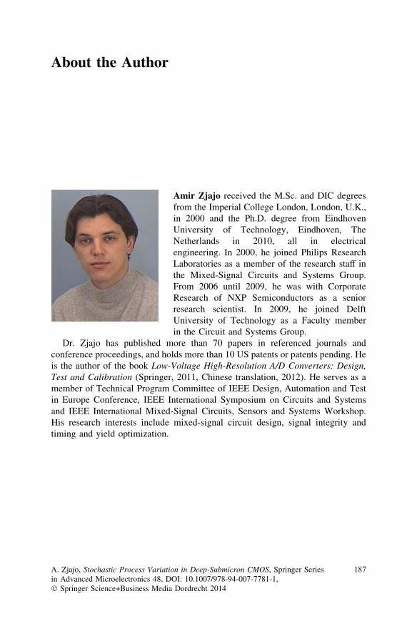
About the Author
Amir Zjajo received the M.Sc. and DIC degreesfrom the Imperial College London, London, U.K.,in 2000 and the Ph.D. degree from EindhovenUniversity of Technology, Eindhoven, TheNetherlands in 2010, all in electricalengineering. In 2000, he joined Philips ResearchLaboratories as a member of the research staff inthe Mixed-Signal Circuits and Systems Group.From 2006 until 2009, he was with CorporateResearch of NXP Semiconductors as a seniorresearch scientist. In 2009, he joined DelftUniversity of Technology as a Faculty memberin the Circuit and Systems Group.
Dr. Zjajo has published more than 70 papers in referenced journals andconference proceedings, and holds more than 10 US patents or patents pending. Heis the author of the book Low-Voltage High-Resolution A/D Converters: Design,Test and Calibration (Springer, 2011, Chinese translation, 2012). He serves as amember of Technical Program Committee of IEEE Design, Automation and Testin Europe Conference, IEEE International Symposium on Circuits and Systemsand IEEE International Mixed-Signal Circuits, Sensors and Systems Workshop.His research interests include mixed-signal circuit design, signal integrity andtiming and yield optimization.
A. Zjajo, Stochastic Process Variation in Deep-Submicron CMOS, Springer Seriesin Advanced Microelectronics 48, DOI: 10.1007/978-94-007-7781-1,� Springer Science+Business Media Dordrecht 2014
187
Index
AAcquisition time, 139Analog to digital converter, 6, 11, 117, 131,
132, 135, 137–139, 141, 143–145, 183Autocorrelation function, 175
BBand-limiting, 7Bartels-Stewart algorithm, 58, 71boosting technique, 129
CCalibration, 3, 7, 11, 123, 124, 132, 135,
136, 141–144, 152, 156Channel leakage, 1, 38Chip multiprocessor, 102Cholesky decomposition, 93Cholesky factor, 34, 36, 58, 59, 71, 80, 98, 107Chopping, 126Circuit simulation, 23, 168Circuit yield, 18, 37Clock period, 39Coarse converter, 96, 131, 132, 141Comparator, 74, 76, 77, 80, 124, 126, 133, 141Comparing random variables , 20, 22, 182Complementary MOS, 1–7, 13, 17, 30, 37, 39,
43–45, 75, 77, 117, 118, 125, 131, 137,146, 149, 151, 153, 154
Computer aided design (CAD), 23, 67Continuous random variable, 20, 22, 42, 182Continuous-time filter, 41, 56, 58, 80, 151Continuous-time integrator, 56Corner analysis, 17Correlation
coefficient, 43function, 20, 22, 57of device parameters , 1, 3, 18, 27, 136
spatial, 27Courant-Friedrichs-Lewy number, 96Covariance, 20, 21, 27, 32, 39, 56, 57, 61,
67, 80, 84, 92–94, 110, 151, 171,175, 176, 184
Crank-Nicolson scheme, 95, 96Critical dimension, 38, 137Cross-coupled latch, 124Cumulative distribution function, 18Cumulative probability, 184
DDesign for testability, 171Device tolerances, 13, 43, 151Device under test, 121, 135, 137, 182Detector, 96, 120, 121, 123, 124Die-level process monitor, 120, 121, 123, 124,
134, 137Differential algebraic equations, 24Differential non-linearity, 137, 139, 140, 185Digital to analog converter, 136Dirichlet boundary condition, 88Discrete random variable, 6, 42, 110Discrete-time filter, 71, 80, 151Discrete-time intagrator, 71, 92Distortion, 6, 8, 68, 119, 134, 135, 144, 145Distribution
across spatial scales, 22arbitrary, 110of device characteristics, 1of device parameters, 1, 3, 18, 27of discrete random variable, 110of noise margins, 38of threshold voltage, 1upper bound on, 8with strong correlations, 13, 143
Drain-induced barrier lowering, 7Dual-residue processing, 132
A. Zjajo, Stochastic Process Variation in Deep-Submicron CMOS, Springer Seriesin Advanced Microelectronics 48, DOI: 10.1007/978-94-007-7781-1,� Springer Science+Business Media Dordrecht 2014
189
Dynamic latch, 74, 77, 80, 122Dynamic range, 4, 6, 7, 10, 135Dynamic voltage-frequency scaling, 102
EEffective channel length, 31, 160Effective number of bits, 135, 183Eigenvalue decomposition, 36Energy optimization, 18, 37, 45, 47, 50, 150Estimator, 45, 60, 66, 109, 134, 182Euler-Maruyama scheme, 63–65Expectation-maximization, 118, 127, 146, 152Extended Kalman filter, 93, 109
FFast fourier transform, 139, 145Figure of merit, 101Fine converter, 132, 141Fitting parameter, 22, 39Forgetting factor, 137Frequency measurements, 4
GGain-bandwidth product, 6Galerkin method, 22, 85, 106, 109Gate length, 1, 7, 17, 27, 149Gate width variability, 9, 119Gaussian mixture model , 128Gradient-search method, 41Gramian, 34–36, 43, 45, 98, 99, 108, 112, 151
HHammarling method, 36, 108Heat source, 14, 84, 87, 89Heuristic approach, 14, 40, 56Hot carrier effect, 7
IIncidence matrix, 25, 62Integral non-linearity, 144Integrated circuit, 1, 2, 13, 14, 17, 24, 49, 56,
57, 60, 85, 91, 110, 117, 133, 149, 150,157
Integrator, 56Interface circuit, 4, 120, 123Interpolation, 30, 32, 86, 97Intra-die, 3, 118, 160Ito stochastic differential equations, 14, 18, 24,
26, 32, 49, 57, 62, 65
JJacobian, 26, 29, 61, 65, 110, 111, 112, 167,
168, 170
KKalman filter, 84, 85, 92, 93, 109, 112, 151Karhunen-Loeve expansion, 20, 22, 39Kirchhoff current law (KCL), 6, 60, 155Kogge-Stone adder, 45, 48, 49, 150
LLeast mean square, 43, 92, 182Least significant bit, 139, 182Linewidth variation, 6Loss function, 134Lyapunov equations, 35, 36, 43, 58, 59
MMatching, 4, 6, 10, 160, 162, 166Manufacturing variations , 22, 91Matrix, 25, 26, 32, 34–37, 43, 56–59Maximum likelihood, 66, 71, 127, 128Mean square error, 43, 92, 182Measurement correction factor , 22Milstein scheme, 64, 65, 79, 80, 150Mobility, 8, 136, 137, 140, 161, 163, 164Mobility reduction, 161Model order reduction, 14, 33, 34, 43, 44, 85,
95, 98, 108, 109, 112, 151Modified nodal analysis, 24, 32Moment estimation, 20, 27, 33Monte-Carlo analysis, 172MOSFET, 1, 3, 4, 137, 152
NNegative bias temperature instability, 13, 83,
117Newton’s method, 19, 24Neyman-Pearson critical region node, 177, 178Nodal analysis, 25, 32, 167Noise
excess factor, 22, 97, 143margins, 6, 75simulation, 55, 70
Non-stationary random process, 153Normal
cumulative distribution function, 18Normal distribution
Central limit theorem, 33Normal random variable, 24, 26
190 Index
OOffset, 5–7, 10, 73, 121, 124–127, 132, 134,
137, 138, 141–143, 160, 164, 165, 181,182
Operational transconductance amplifier, 126Optimization
deterministic, 18, 37sensitivity-driven, 37stochastic, 18, 49, 150
Ordinary differential equations, 24, 57, 65, 85,89
PParameter vector, 65, 66, 127, 128, 169, 170Parameter space, 23, 28, 49, 128, 150Parametric functions, 13, 20, 176Parametric yield, 23Parametric yield loss
impact of gate length variability, 17impact of gate length variation, 17, 20, 27impact of power variability, 155
Parametric yield metric, 23Parametric yield optimization, 23Partial differential equations, 24, 85Power
dynamic, 3, 92, 103, 117, 124static, 49, 150
Power management block, 103Printed circuit board, 134Probability density function, 26, 40, 62, 92, 93,
135, 169, 182Probability distribution, 18Process control monitor, 119Process variation, 1, 3, 10–14, 17, 18, 25,
27–29, 31, 32, 37, 38, 42, 43Process window programmable gain amplifier,
73Processing elements, 85, 86, 90, 91Proportional to absolute temperature, 125, 126Pseudo-noise sequence, 79
QQuadratic programming, 41, 130Quality factor , 69Quantizer, 132, 135, 182, 183
RRandom error, 10Random dopant fluctuation, 2, 4, 12Random function, 25, 57, 169
Random gate length variation, 3, 10, 17, 37,160
Random intra chip variability, 3, 10, 20, 22,33, 162
Random process, 20, 22, 31Random sampling, 180Random variability, 20, 21, 39, 63, 110, 182Random variables, 20–22, 39, 63, 110Random vector, 25, 26, 40, 42, 469Random telegraph noise, 2, 4, 152, 153Reliability, 10, 13, 41, 63, 83, 84, 117, 149,
152, 154Representations of random variableResiduals, 43, 44, 61, 88, 89, 107, 108, 144Riccati equation, 98, 107, 108, 112, 151Runge-Kutta method, 14, 57, 85, 86Runtime, 30, 48, 84, 90, 92, 100–103, 111
SSchur decomposition, 58, 71Sensors, 3, 84, 90–92, 109, 110, 112, 137, 141,
151Short-channel effects, 1, 38Signal to noise and distortion, 183Signal to noise ratio, 8, 9, 144, 145Signal to noise plus distortion ratio, 145Significance level, 178, 179Singular value decomposition, 34, 99Spatial correlation, 10, 22, 27Spatial distribution, 18, 20, 31, 33, 39, 42, 43,
47, 109, 110, 140, 162, 163, 165, 166,184
Spurious free dynamic range, 135, 144, 145Standard deviation, 18, 20, 31, 33, 39, 42, 43,
47, 110, 140Static latch, 27, 77Stationary random process, 153Statistical timing analysis, 14, 18, 27, 29, 32,
33, 42, 49, 150Steepest descent method, 136Stochastic differential equations, 14, 18, 24,
26, 32, 49, 56, 62, 150Stochastic process, 1, 20, 33, 57, 175Support vector machine, 118, 129, 146, 152Surface potential based models, 118, 129, 146,
152, 142Switched capacitor, 67, 71–73System on chip, 3Systematic drift, 136Systematic impact of layout, 127Systematic spatial variation, 20Systematic variability, 20
Index 191
TTaylor series, 70, 77, 84, 93, 95Thermal management, 4, 13, 83, 90, 102, 110,
117, 149, 151Temperature monitor, 125, 126, 132, 140Temperature variability, 14, 155Test control block, 120, 123, 141Test structures, 137Threshold voltage, 1, 3, 11, 17–19, 21, 22, 31,
37–19, 47, 60, 117, 119, 127, 136, 137,140, 149, 152, 155, 157
Threshold voltage based models, 19, 60Time to digital converter, 118, 146, 155, 156Tolerance, 13, 23, 49, 107, 142, 169, 172, 176Total harmonic distortion, 135Transconductor, 68Transient analysis, 26, 29, 32, 56Transistor model, 24, 29, 42, 49, 150, 157, 158Truncated balanced realization, 34, 108, 109,
112, 151
UUnbiased estimator, 179Unscented kalman filter, 14, 93, 109
Unscented transform, 93, 109
VVariable gain amplifier, 42, 71, 73–75, 80, 151Very large-scale integrated circuit, 91, 92, 117,
127, 132Voltage variability, 2, 3, 12, 17
WWafer, 3, 20, 118, 119, 139, 166Wiener process, 57, 63–65Within-die, 4, 91Worst-case analysis, 23, 127
YYield, 1, 2, 6, 10, 13, 14, 18, 19, 23, 24, 32, 37,
38
ZZero-crossing, 135
192 Index