Embed Size (px)
Citation preview
ATLCE - B1 19/03/2012
© 2012 DDC 1
19/03/2012 - 1 ATLCE - B1 - © 2012 DDC
Politecnico di Torino - ICT School
Analog and Telecommunication Electronics
B1 - Radio systems architecture
» Basic radio systems
» Image rejection
» Digital and SW radio
» Functional units
ATLCE - B1 19/03/2012
© 2012 DDC 2
19/03/2012 - 2 ATLCE - B1 - © 2012 DDC
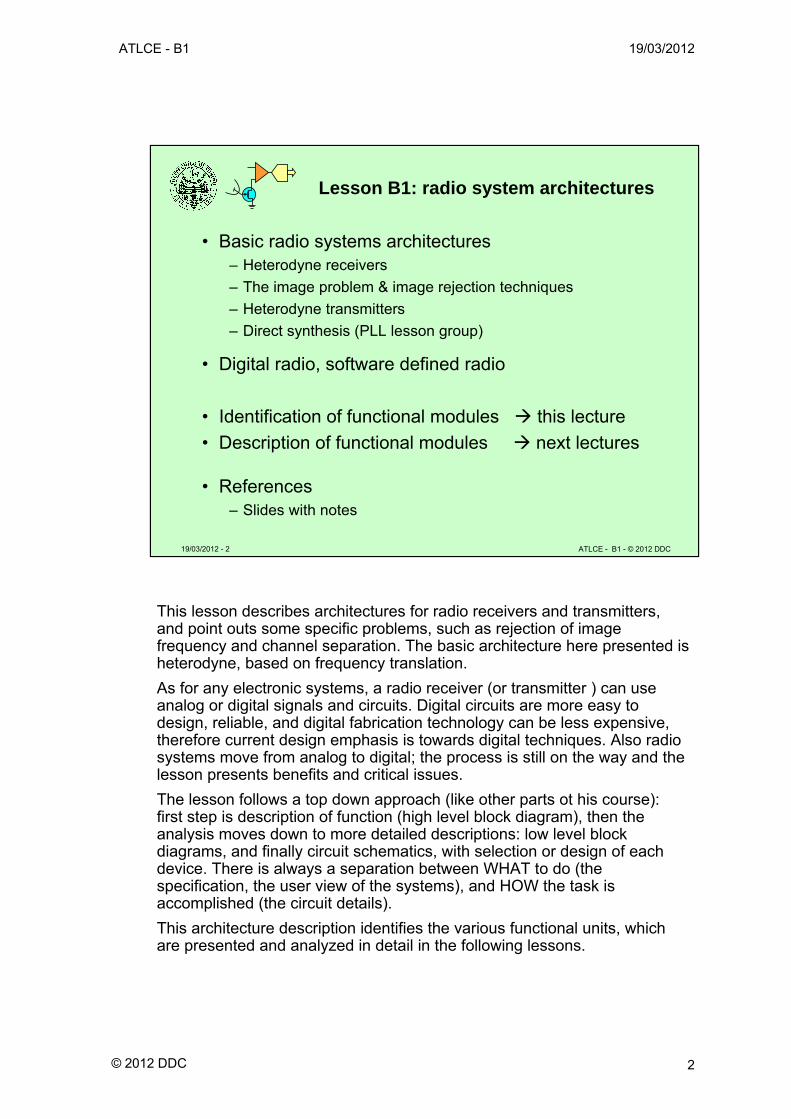
Lesson B1: radio system architectures
• Basic radio systems architectures– Heterodyne receivers
– The image problem & image rejection techniques
– Heterodyne transmitters
– Direct synthesis (PLL lesson group)
• Digital radio, software defined radio
• Identification of functional modules this lecture
• Description of functional modules next lectures
• References– Slides with notes
This lesson describes architectures for radio receivers and transmitters, and point outs some specific problems, such as rejection of image frequency and channel separation. The basic architecture here presented is heterodyne, based on frequency translation.
As for any electronic systems, a radio receiver (or transmitter ) can use analog or digital signals and circuits. Digital circuits are more easy to design, reliable, and digital fabrication technology can be less expensive, therefore current design emphasis is towards digital techniques. Also radio systems move from analog to digital; the process is still on the way and the lesson presents benefits and critical issues.
The lesson follows a top down approach (like other parts ot his course): first step is description of function (high level block diagram), then the analysis moves down to more detailed descriptions: low level block diagrams, and finally circuit schematics, with selection or design of each device. There is always a separation between WHAT to do (the specification, the user view of the systems), and HOW the task is accomplished (the circuit details).
This architecture description identifies the various functional units, which are presented and analyzed in detail in the following lessons.
ATLCE - B1 19/03/2012
© 2012 DDC 3
19/03/2012 - 3 ATLCE - B1 - © 2012 DDC
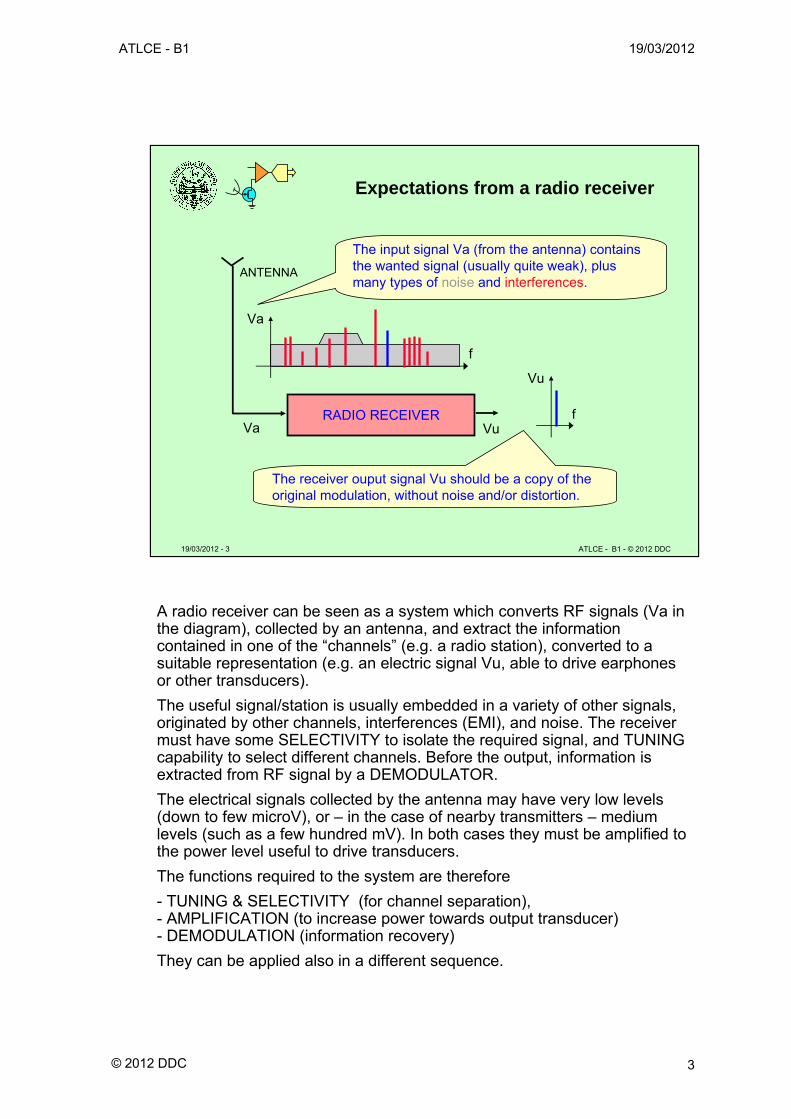
Expectations from a radio receiver
Vu
ANTENNA
RADIO RECEIVERVa
f
Va
The input signal Va (from the antenna) containsthe wanted signal (usually quite weak), plus many types of noise and interferences.
f
Vu
The receiver ouput signal Vu should be a copy of the original modulation, without noise and/or distortion.
A radio receiver can be seen as a system which converts RF signals (Va in the diagram), collected by an antenna, and extract the information contained in one of the “channels” (e.g. a radio station), converted to a suitable representation (e.g. an electric signal Vu, able to drive earphones or other transducers).
The useful signal/station is usually embedded in a variety of other signals, originated by other channels, interferences (EMI), and noise. The receiver must have some SELECTIVITY to isolate the required signal, and TUNING capability to select different channels. Before the output, information is extracted from RF signal by a DEMODULATOR.
The electrical signals collected by the antenna may have very low levels (down to few microV), or – in the case of nearby transmitters – medium levels (such as a few hundred mV). In both cases they must be amplified to the power level useful to drive transducers.
The functions required to the system are therefore
- TUNING & SELECTIVITY (for channel separation), - AMPLIFICATION (to increase power towards output transducer)- DEMODULATION (information recovery)
They can be applied also in a different sequence.
ATLCE - B1 19/03/2012
© 2012 DDC 4
19/03/2012 - 4 ATLCE - B1 - © 2012 DDC
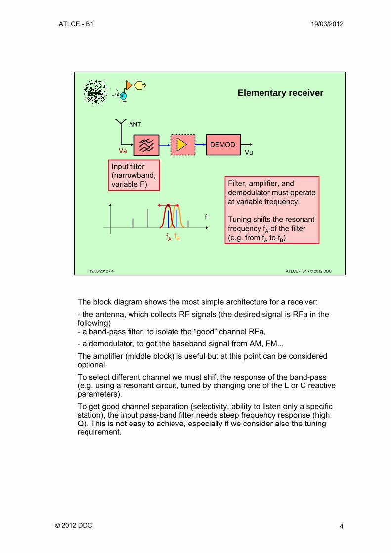
Elementary receiver
Filter, amplifier, and demodulator must operate at variable frequency.
Tuning shifts the resonant frequency fA of the filter(e.g. from fA to fB)
Vu
ANT.
DEMOD.Va
f
fA
Input filter(narrowband, variable F)
fB
The block diagram shows the most simple architecture for a receiver:
- the antenna, which collects RF signals (the desired signal is RFa in the following)- a band-pass filter, to isolate the “good” channel RFa,
- a demodulator, to get the baseband signal from AM, FM...
The amplifier (middle block) is useful but at this point can be considered optional.
To select different channel we must shift the response of the band-pass (e.g. using a resonant circuit, tuned by changing one of the L or C reactive parameters).
To get good channel separation (selectivity, ability to listen only a specific station), the input pass-band filter needs steep frequency response (high Q). This is not easy to achieve, especially if we consider also the tuning requirement.
ATLCE - B1 19/03/2012
© 2012 DDC 5
19/03/2012 - 5 ATLCE - B1 - © 2012 DDC
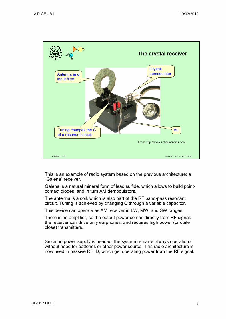
The crystal receiver
From http://www.antiqueradios.com
Antenna and input filter
Tuning changes the C of a resonant circuit
Vu
Crystal demodulator
This is an example of radio system based on the previous architecture: a “Galena” receiver.
Galena is a natural mineral form of lead sulfide, which allows to build point-contact diodes, and in turn AM demodulators.
The antenna is a coil, which is also part of the RF band-pass resonant circuit. Tuning is achieved by changing C through a variable capacitor.
This device can operate as AM receiver in LW, MW, and SW ranges.
There is no amplifier, so the output power comes directly from RF signal: the receiver can drive only earphones, and requires high power (or quite close) transmitters.
Since no power supply is needed, the system remains always operational, without need for batteries or other power source. This radio architecture is now used in passive RF ID, which get operating power from the RF signal.
ATLCE - B1 19/03/2012
© 2012 DDC 6
19/03/2012 - 6 ATLCE - B1 - © 2012 DDC
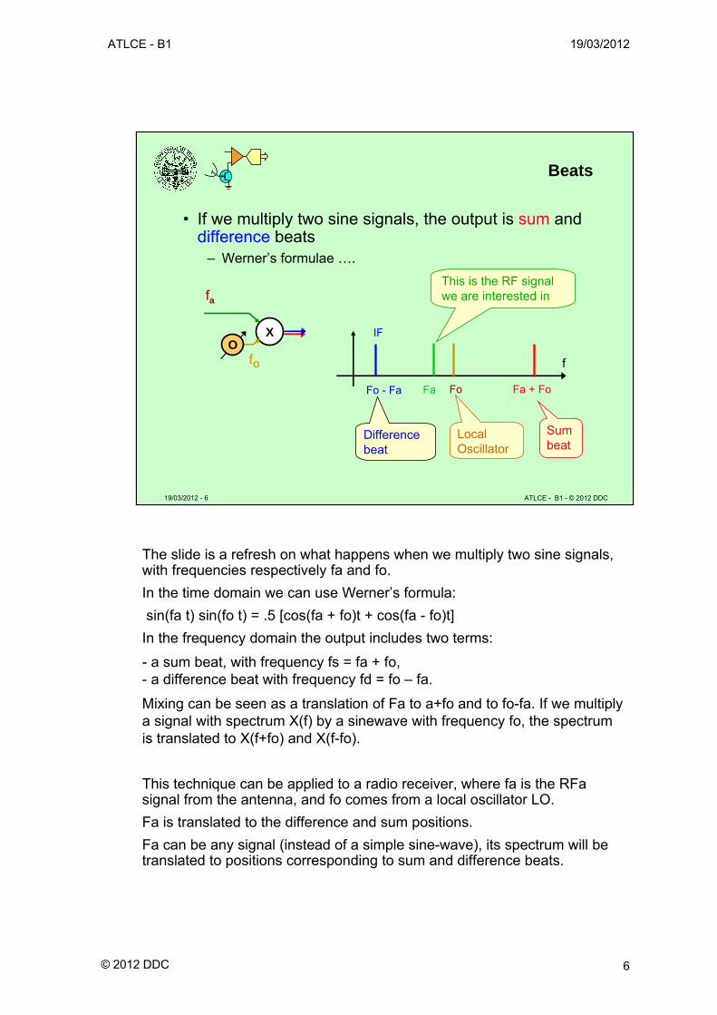
Beats
• If we multiply two sine signals, the output is sum and difference beats
– Werner’s formulae ….-:
f
FaFo - Fa Fo Fa + Fo
IF
This is the RF signalwe are interested in
Differencebeat
Sum beat
LocalOscillator
X
fa
fOO
The slide is a refresh on what happens when we multiply two sine signals, with frequencies respectively fa and fo.
In the time domain we can use Werner’s formula:
sin(fa t) sin(fo t) = .5 [cos(fa + fo)t + cos(fa - fo)t]
In the frequency domain the output includes two terms:
- a sum beat, with frequency fs = fa + fo, - a difference beat with frequency fd = fo – fa.
Mixing can be seen as a translation of Fa to a+fo and to fo-fa. If we multiply a signal with spectrum X(f) by a sinewave with frequency fo, the spectrum is translated to X(f+fo) and X(f-fo).
This technique can be applied to a radio receiver, where fa is the RFasignal from the antenna, and fo comes from a local oscillator LO.
Fa is translated to the difference and sum positions.
Fa can be any signal (instead of a simple sine-wave), its spectrum will be translated to positions corresponding to sum and difference beats.
ATLCE - B1 19/03/2012
© 2012 DDC 7
19/03/2012 - 7 ATLCE - B1 - © 2012 DDC
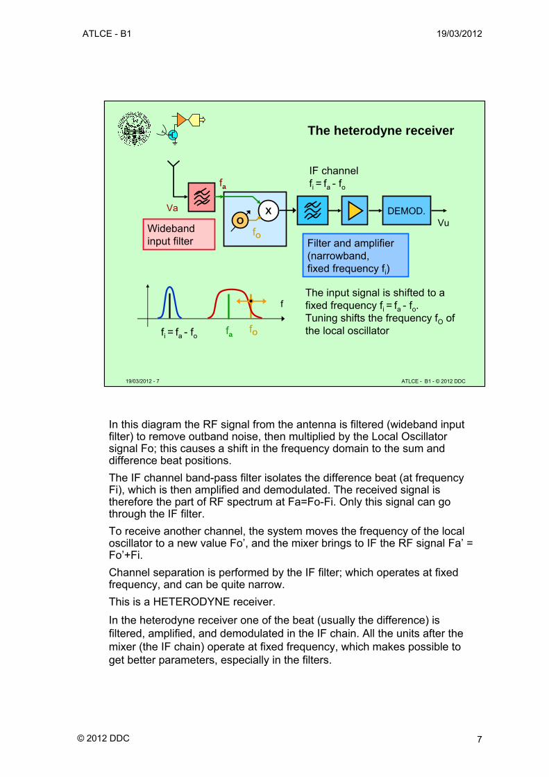
The heterodyne receiver
The input signal is shifted to a fixed frequency fi = fa - fo.Tuning shifts the frequency fO of the local oscillator
Wideband input filter
X DEMOD.Va
Vu
Filter and amplifier (narrowband, fixed frequency fi)
f
fa fOfi = fa - fo
fa
fO
IF channelfi = fa - fo
O
In this diagram the RF signal from the antenna is filtered (wideband input filter) to remove outband noise, then multiplied by the Local Oscillator signal Fo; this causes a shift in the frequency domain to the sum and difference beat positions.
The IF channel band-pass filter isolates the difference beat (at frequency Fi), which is then amplified and demodulated. The received signal is therefore the part of RF spectrum at Fa=Fo-Fi. Only this signal can go through the IF filter.
To receive another channel, the system moves the frequency of the local oscillator to a new value Fo’, and the mixer brings to IF the RF signal Fa’ = Fo’+Fi.
Channel separation is performed by the IF filter; which operates at fixed frequency, and can be quite narrow.
This is a HETERODYNE receiver.
In the heterodyne receiver one of the beat (usually the difference) is filtered, amplified, and demodulated in the IF chain. All the units after the mixer (the IF chain) operate at fixed frequency, which makes possible to get better parameters, especially in the filters.
ATLCE - B1 19/03/2012
© 2012 DDC 8
19/03/2012 - 8 ATLCE - B1 - © 2012 DDC
Not so new …
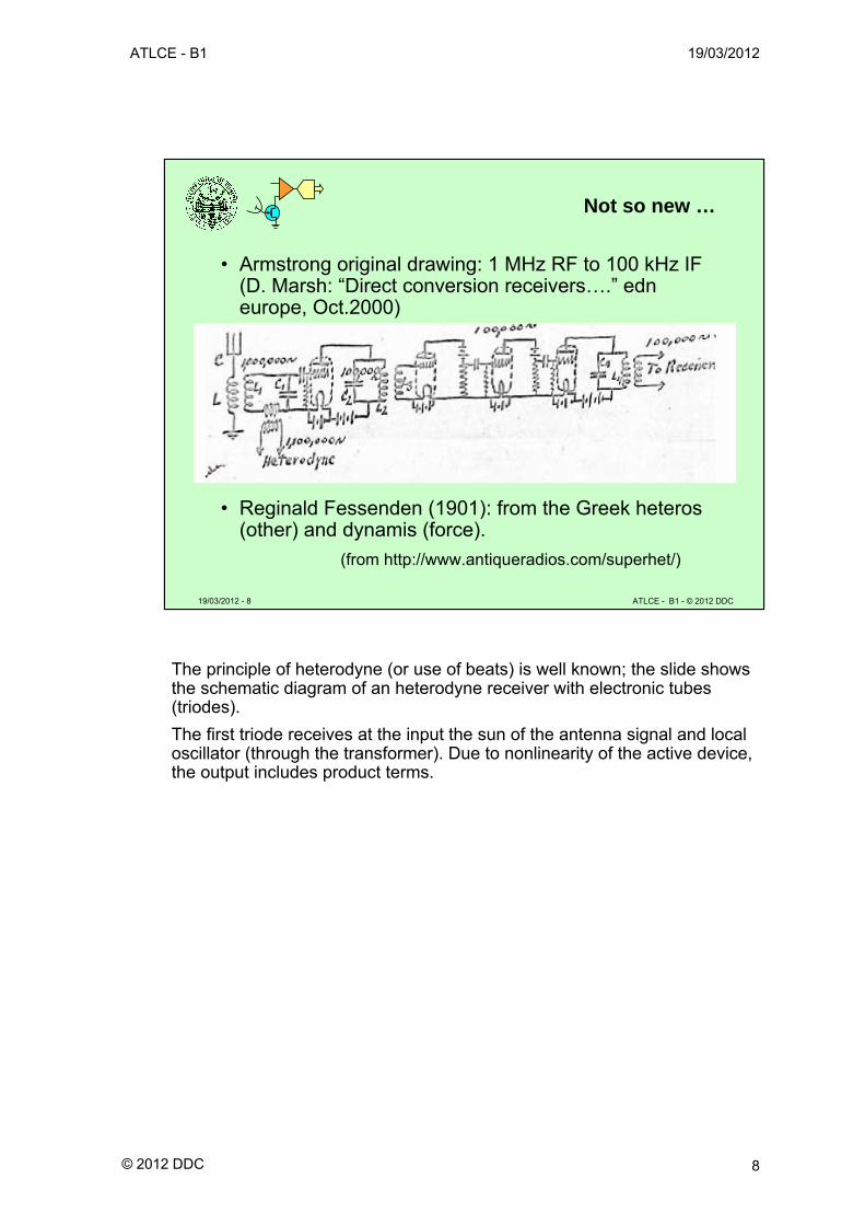
• Armstrong original drawing: 1 MHz RF to 100 kHz IF (D. Marsh: “Direct conversion receivers….” edneurope, Oct.2000)
• Reginald Fessenden (1901): from the Greek heteros(other) and dynamis (force).
(from http://www.antiqueradios.com/superhet/)
The principle of heterodyne (or use of beats) is well known; the slide shows the schematic diagram of an heterodyne receiver with electronic tubes (triodes).
The first triode receives at the input the sun of the antenna signal and local oscillator (through the transformer). Due to nonlinearity of the active device, the output includes product terms.
ATLCE - B1 19/03/2012
© 2012 DDC 9
19/03/2012 - 9 ATLCE - B1 - © 2012 DDC
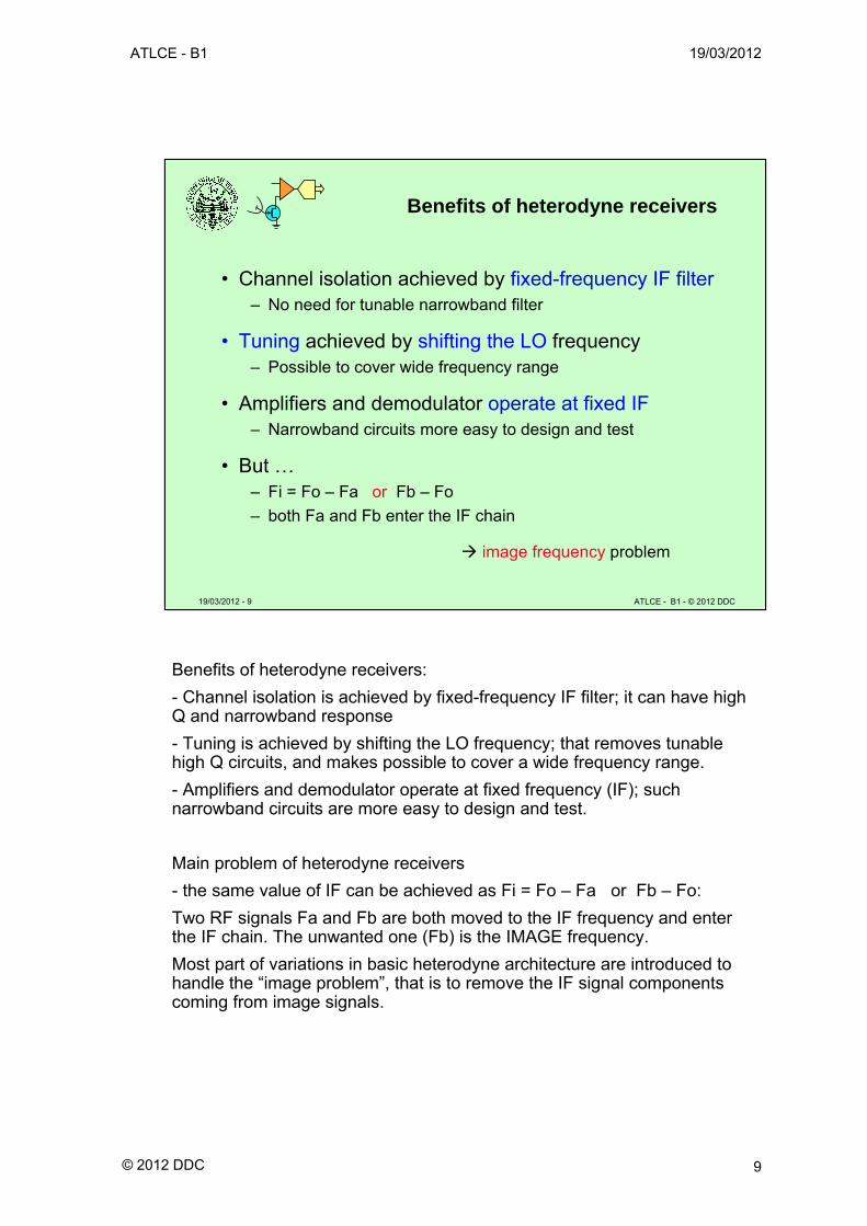
Benefits of heterodyne receivers
• Channel isolation achieved by fixed-frequency IF filter– No need for tunable narrowband filter
• Tuning achieved by shifting the LO frequency– Possible to cover wide frequency range
• Amplifiers and demodulator operate at fixed IF– Narrowband circuits more easy to design and test
• But …– Fi = Fo – Fa or Fb – Fo
– both Fa and Fb enter the IF chain
image frequency problem
Benefits of heterodyne receivers:
- Channel isolation is achieved by fixed-frequency IF filter; it can have high Q and narrowband response
- Tuning is achieved by shifting the LO frequency; that removes tunable high Q circuits, and makes possible to cover a wide frequency range.
- Amplifiers and demodulator operate at fixed frequency (IF); such narrowband circuits are more easy to design and test.
Main problem of heterodyne receivers
- the same value of IF can be achieved as Fi = Fo – Fa or Fb – Fo:
Two RF signals Fa and Fb are both moved to the IF frequency and enter the IF chain. The unwanted one (Fb) is the IMAGE frequency.
Most part of variations in basic heterodyne architecture are introduced to handle the “image problem”, that is to remove the IF signal components coming from image signals.
ATLCE - B1 19/03/2012
© 2012 DDC 10
19/03/2012 - 10 ATLCE - B1 - © 2012 DDC
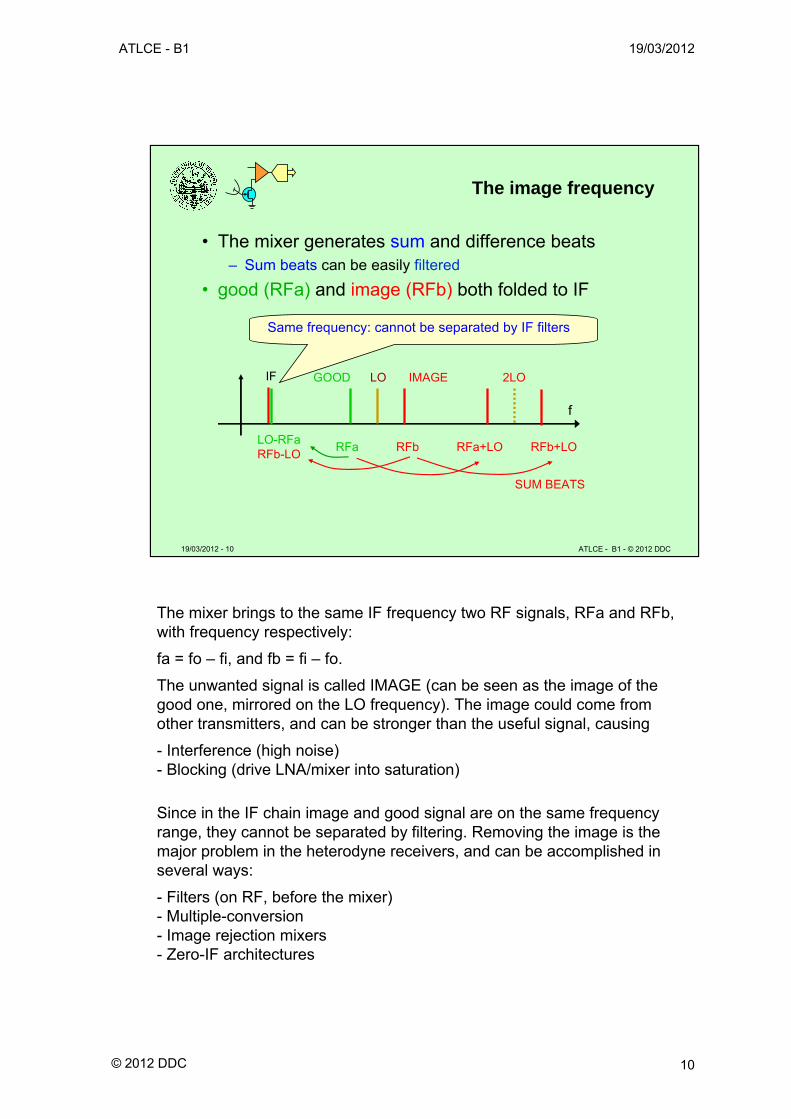
The image frequency
• The mixer generates sum and difference beats– Sum beats can be easily filtered
• good (RFa) and image (RFb) both folded to IF-:
f
RFa RFbLO-RFaRFb-LO
LO 2LO
RFa+LO RFb+LO
GOOD IMAGE
SUM BEATS
IF
Same frequency: cannot be separated by IF filters
The mixer brings to the same IF frequency two RF signals, RFa and RFb, with frequency respectively:
fa = fo – fi, and fb = fi – fo.
The unwanted signal is called IMAGE (can be seen as the image of the good one, mirrored on the LO frequency). The image could come from other transmitters, and can be stronger than the useful signal, causing
- Interference (high noise)- Blocking (drive LNA/mixer into saturation)
Since in the IF chain image and good signal are on the same frequency range, they cannot be separated by filtering. Removing the image is the major problem in the heterodyne receivers, and can be accomplished in several ways:
- Filters (on RF, before the mixer)- Multiple-conversion- Image rejection mixers- Zero-IF architectures
ATLCE - B1 19/03/2012
© 2012 DDC 11
19/03/2012 - 11 ATLCE - B1 - © 2012 DDC
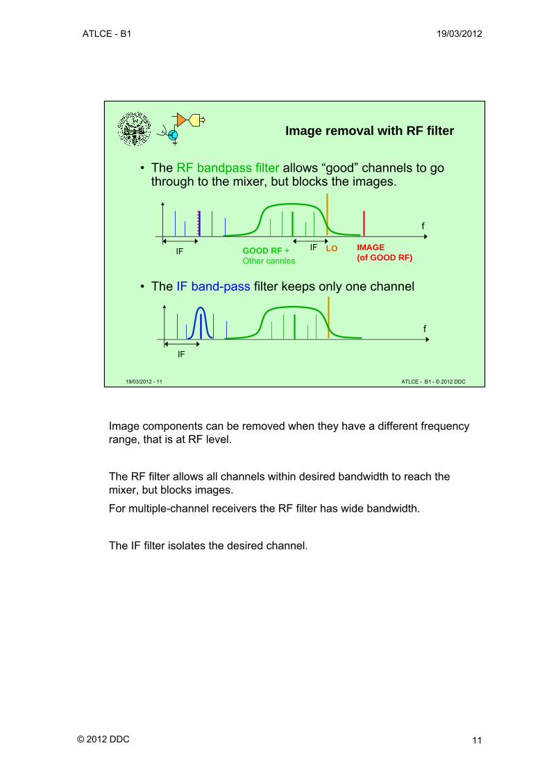
Image removal with RF filter
• The RF bandpass filter allows “good” channels to go through to the mixer, but blocks the images.
• The IF band-pass filter keeps only one channel
GOOD RF +Other cannles
f
LO IMAGE (of GOOD RF)
IF IF
f
IF
Image components can be removed when they have a different frequency range, that is at RF level.
The RF filter allows all channels within desired bandwidth to reach the mixer, but blocks images.
For multiple-channel receivers the RF filter has wide bandwidth.
The IF filter isolates the desired channel.
ATLCE - B1 19/03/2012
© 2012 DDC 12
19/03/2012 - 12 ATLCE - B1 - © 2012 DDC
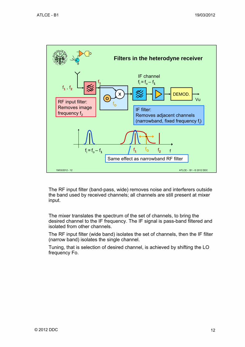
Filters in the heterodyne receiver
RF input filter:Removes image frequency f2
XO
DEMOD.Vu
IF filter:Removes adjacent channels (narrowband, fixed frequency fi)
f1
fO
IF channelfI = fo – f1
ff1 fOfi = fo – f1 f2
f1 , f2
Same effect as narrowband RF filter
The RF input filter (band-pass, wide) removes noise and interferers outside the band used by received channels; all channels are still present at mixer input.
The mixer translates the spectrum of the set of channels, to bring the desired channel to the IF frequency. The IF signal is pass-band filtered and isolated from other channels.
The RF input filter (wide band) isolates the set of channels, then the IF filter (narrow band) isolates the single channel.
Tuning, that is selection of desired channel, is achieved by shifting the LO frequency Fo.
ATLCE - B1 19/03/2012
© 2012 DDC 13
19/03/2012 - 13 ATLCE - B1 - © 2012 DDC
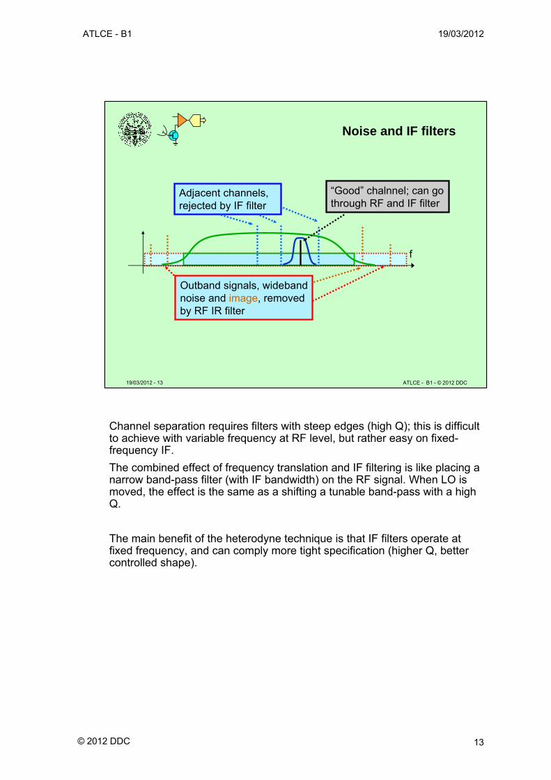
Noise and IF filters
f
Outband signals, wideband noise and image, removed by RF IR filter
Adjacent channels, rejected by IF filter
“Good” chalnnel; can go through RF and IF filter
Channel separation requires filters with steep edges (high Q); this is difficult to achieve with variable frequency at RF level, but rather easy on fixed-frequency IF.
The combined effect of frequency translation and IF filtering is like placing a narrow band-pass filter (with IF bandwidth) on the RF signal. When LO is moved, the effect is the same as a shifting a tunable band-pass with a high Q.
The main benefit of the heterodyne technique is that IF filters operate at fixed frequency, and can comply more tight specification (higher Q, better controlled shape).
ATLCE - B1 19/03/2012
© 2012 DDC 14
19/03/2012 - 14 ATLCE - B1 - © 2012 DDC
Lesson B1: radio system architectures
• Heterodyne receivers
• The image problem
• Dual conversion receivers
• Complex mixer & I/Q processing
• Digital receivers
• Software Defined Radio
• Examples
ATLCE - B1 19/03/2012
© 2012 DDC 15
19/03/2012 - 15 ATLCE - B1 - © 2012 DDC
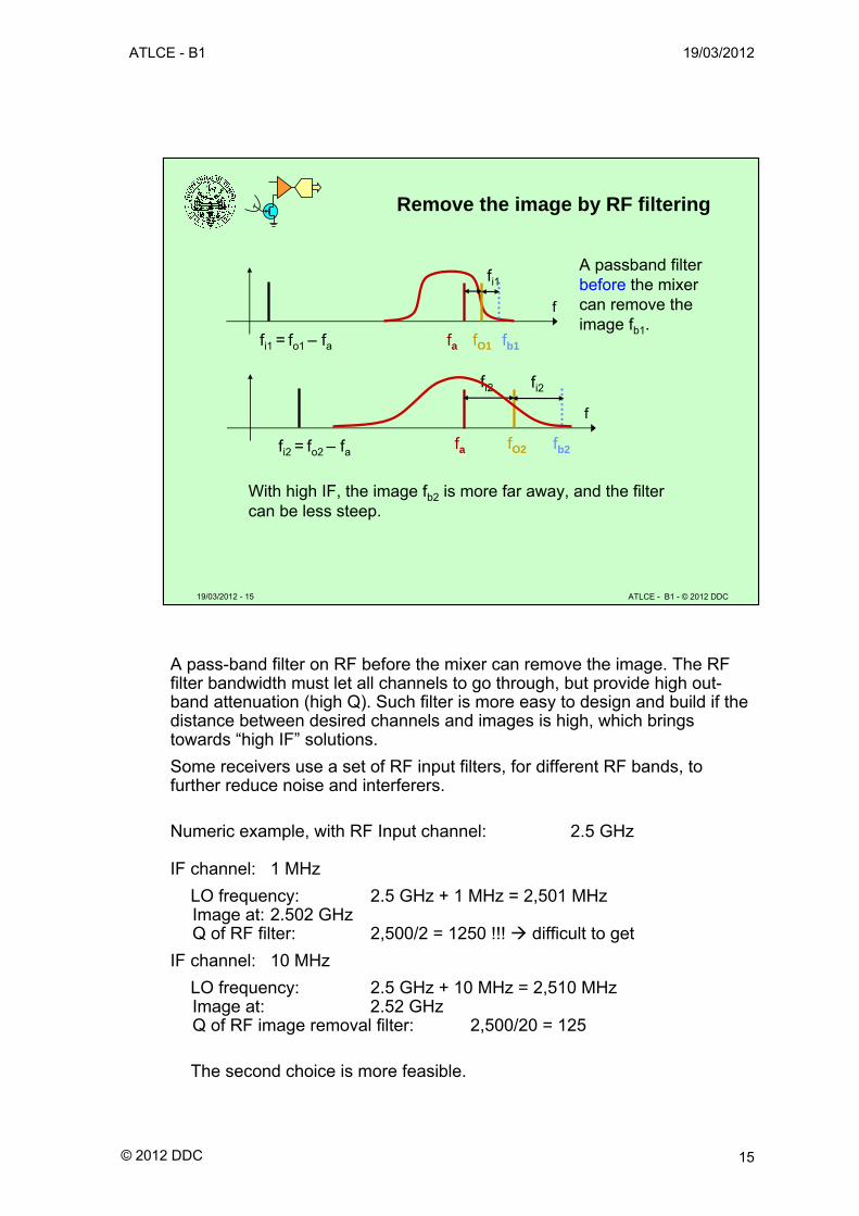
Remove the image by RF filtering
With high IF, the image fb2 is more far away, and the filter can be less steep.
f
fi1 = fo1 – fa fa fO1 fb1
fi1
f
fa fO2 fb2
fi2 fi2
A passband filter before the mixer can remove the image fb1.
fi2 = fo2 – fa
A pass-band filter on RF before the mixer can remove the image. The RF filter bandwidth must let all channels to go through, but provide high out-band attenuation (high Q). Such filter is more easy to design and build if the distance between desired channels and images is high, which brings towards “high IF” solutions.
Some receivers use a set of RF input filters, for different RF bands, to further reduce noise and interferers.
Numeric example, with RF Input channel: 2.5 GHz
IF channel: 1 MHz
LO frequency: 2.5 GHz + 1 MHz = 2,501 MHz Image at: 2.502 GHzQ of RF filter: 2,500/2 = 1250 !!! difficult to get
IF channel: 10 MHz
LO frequency: 2.5 GHz + 10 MHz = 2,510 MHz Image at: 2.52 GHzQ of RF image removal filter: 2,500/20 = 125
The second choice is more feasible.
ATLCE - B1 19/03/2012
© 2012 DDC 16
19/03/2012 - 16 ATLCE - B1 - © 2012 DDC
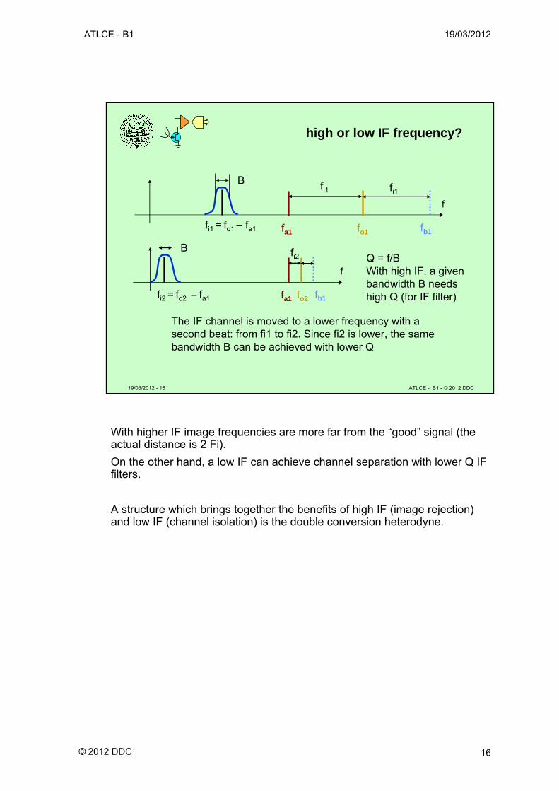
high or low IF frequency?
The IF channel is moved to a lower frequency with a second beat: from fi1 to fi2. Since fi2 is lower, the same bandwidth B can be achieved with lower Q
Q = f/BWith high IF, a given bandwidth B needs high Q (for IF filter)
f
fi1 = fo1 – fa1
f
fi2 = fo2 – fa1 fa1 fo2 fb1
fi2
B
B
fa1 fo1 fb1
fi1 fi1
With higher IF image frequencies are more far from the “good” signal (the actual distance is 2 Fi).
On the other hand, a low IF can achieve channel separation with lower Q IF filters.
A structure which brings together the benefits of high IF (image rejection) and low IF (channel isolation) is the double conversion heterodyne.
ATLCE - B1 19/03/2012
© 2012 DDC 17
19/03/2012 - 17 ATLCE - B1 - © 2012 DDC
fi2
= fi1 – fO2
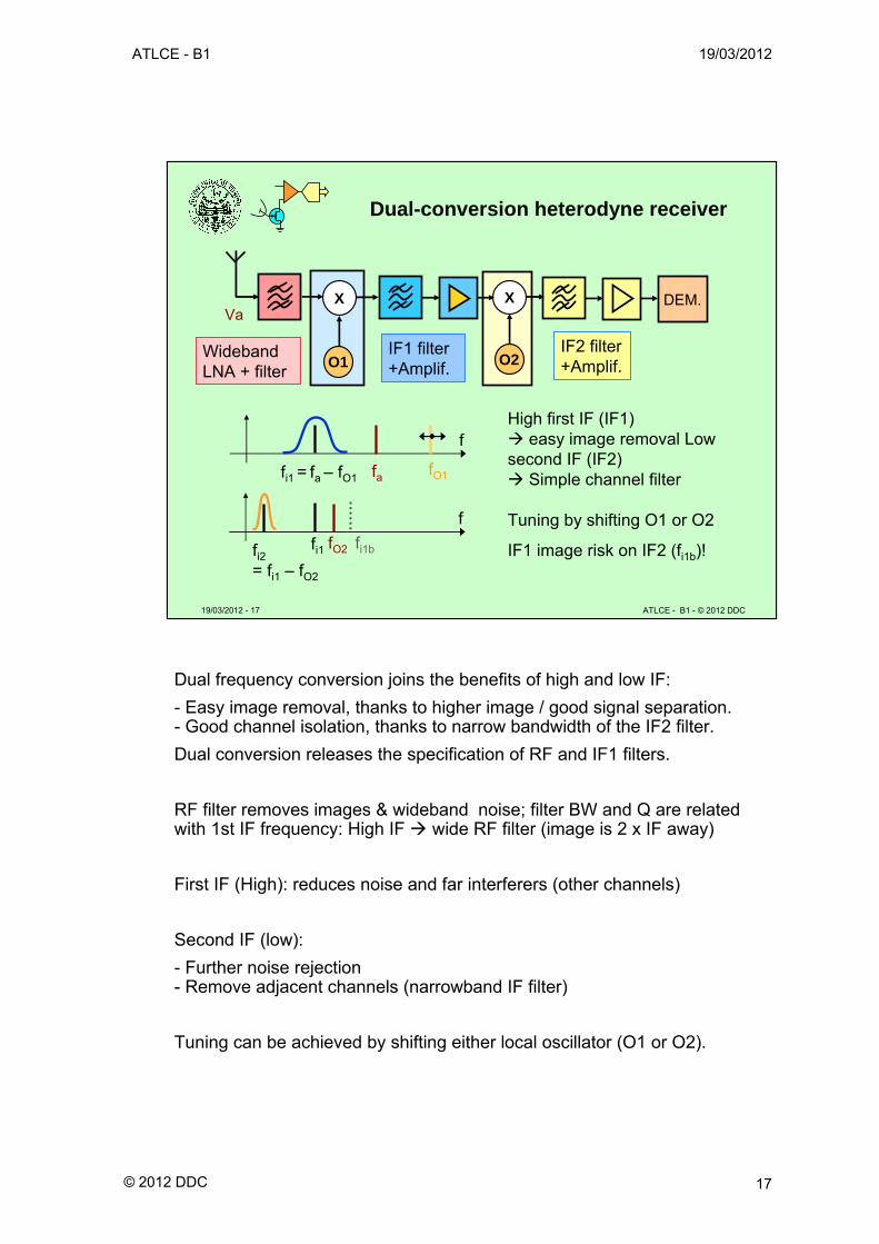
Dual-conversion heterodyne receiver
High first IF (IF1) easy image removal Low second IF (IF2) Simple channel filter
Tuning by shifting O1 or O2
IF1 image risk on IF2 (fi1b)!
WidebandLNA + filter
X
O1
DEM.Va
IF1 filter +Amplif.
f
fa fO1fi1 = fa – fO1
X
O2IF2 filter +Amplif.
f
fO2fi1 fi1b
Dual frequency conversion joins the benefits of high and low IF:
- Easy image removal, thanks to higher image / good signal separation.- Good channel isolation, thanks to narrow bandwidth of the IF2 filter.
Dual conversion releases the specification of RF and IF1 filters.
RF filter removes images & wideband noise; filter BW and Q are related with 1st IF frequency: High IF wide RF filter (image is 2 x IF away)
First IF (High): reduces noise and far interferers (other channels)
Second IF (low):
- Further noise rejection- Remove adjacent channels (narrowband IF filter)
Tuning can be achieved by shifting either local oscillator (O1 or O2).
ATLCE - B1 19/03/2012
© 2012 DDC 18
19/03/2012 - 18 ATLCE - B1 - © 2012 DDC
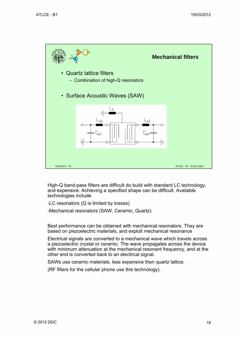
Mechanical filters
• Quartz lattice filters– Combination of high-Q resonators
• Surface Acoustic Waves (SAW)
High-Q band-pass filters are difficult do build with standard LC technology,and expensive. Achieving a specified shape can be difficult. Available technologies include
-LC resonators (Q is limited by losses)
-Mechanical resonators (SAW, Ceramic, Quartz)
Best performance can be obtained with mechanical resonators. They are based on piezoelectric materials, and exploit mechanical resonance
Electrical signals are converted to a mechanical wave which travels across a piezoelectric crystal or ceramic. The wave propagates across the device with minimum attenuation at the mechanical resonant frequency, and at the other end is converted back to an electrical signal.
SAWs use ceramic materials, less expensive then quartz lattice.
(RF filters for the cellular phone use this technology).
ATLCE - B1 19/03/2012
© 2012 DDC 19
19/03/2012 - 19 ATLCE - B1 - © 2012 DDC
:
Complex mixers: SSB & image reject
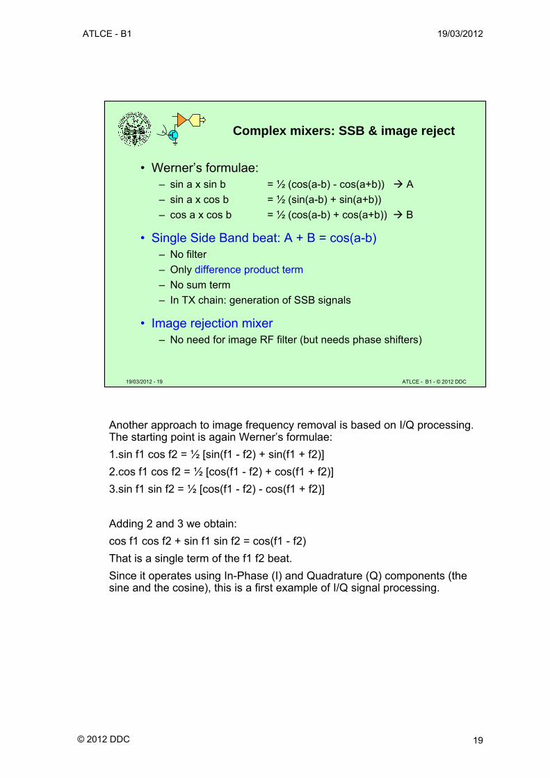
• Werner’s formulae:– sin a x sin b = ½ (cos(a-b) - cos(a+b)) A
– sin a x cos b = ½ (sin(a-b) + sin(a+b))
– cos a x cos b = ½ (cos(a-b) + cos(a+b)) B
• Single Side Band beat: A + B = cos(a-b)– No filter
– Only difference product term
– No sum term
– In TX chain: generation of SSB signals
• Image rejection mixer– No need for image RF filter (but needs phase shifters)
-:
-
Another approach to image frequency removal is based on I/Q processing. The starting point is again Werner’s formulae:
1.sin f1 cos f2 = ½ [sin(f1 - f2) + sin(f1 + f2)]
2.cos f1 cos f2 = ½ [cos(f1 - f2) + cos(f1 + f2)]
3.sin f1 sin f2 = ½ [cos(f1 - f2) - cos(f1 + f2)]
Adding 2 and 3 we obtain:
cos f1 cos f2 + sin f1 sin f2 = cos(f1 - f2)
That is a single term of the f1 f2 beat.
Since it operates using In-Phase (I) and Quadrature (Q) components (the sine and the cosine), this is a first example of I/Q signal processing.
ATLCE - B1 19/03/2012
© 2012 DDC 20
19/03/2012 - 20 ATLCE - B1 - © 2012 DDC
I/Q mixer in receivers
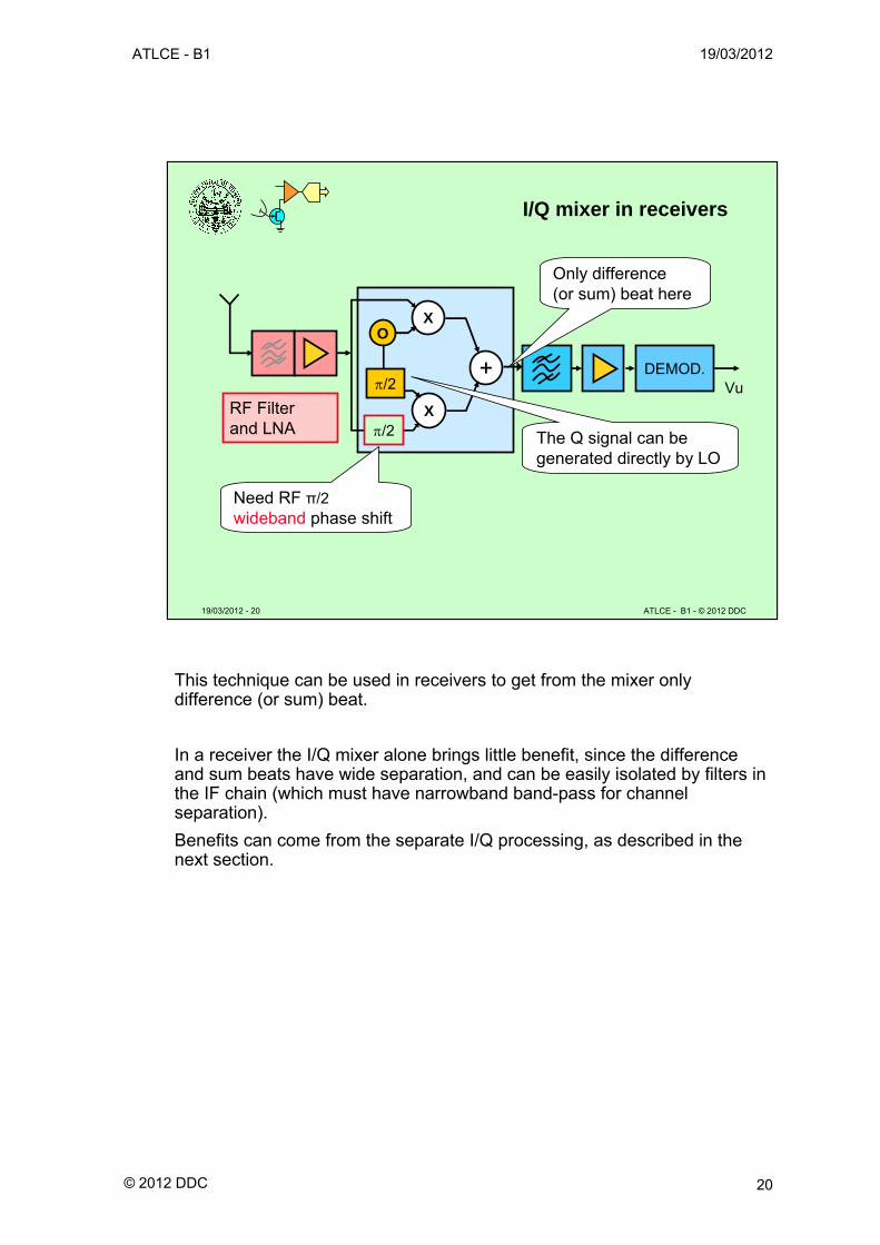
RF Filter and LNA
X
XO
/2DEMOD.
Vu+
/2
Need RF π/2 wideband phase shift
Only difference (or sum) beat here
The Q signal can be generated directly by LO
This technique can be used in receivers to get from the mixer only difference (or sum) beat.
In a receiver the I/Q mixer alone brings little benefit, since the difference and sum beats have wide separation, and can be easily isolated by filters in the IF chain (which must have narrowband band-pass for channel separation).
Benefits can come from the separate I/Q processing, as described in the next section.
ATLCE - B1 19/03/2012
© 2012 DDC 21
19/03/2012 - 21 ATLCE - B1 - © 2012 DDC
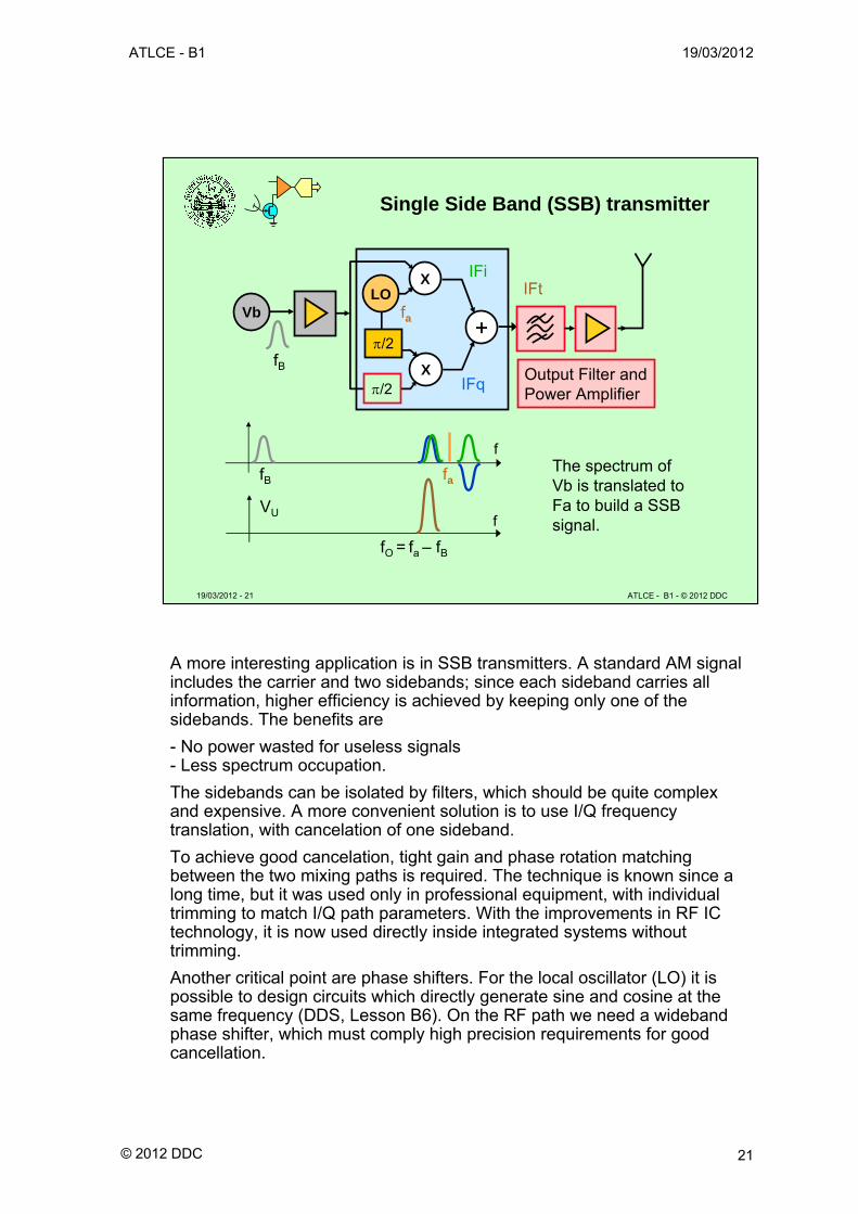
Single Side Band (SSB) transmitter
Output Filter and Power Amplifier
X
X
/2+
/2
LOVb
f
fB fa
fO = fa – fB
fVU
The spectrum of Vb is translated to Fa to build a SSB signal.
fa
fB
IFi
IFq
IFt
A more interesting application is in SSB transmitters. A standard AM signal includes the carrier and two sidebands; since each sideband carries all information, higher efficiency is achieved by keeping only one of the sidebands. The benefits are
- No power wasted for useless signals- Less spectrum occupation.
The sidebands can be isolated by filters, which should be quite complex and expensive. A more convenient solution is to use I/Q frequency translation, with cancelation of one sideband.
To achieve good cancelation, tight gain and phase rotation matching between the two mixing paths is required. The technique is known since a long time, but it was used only in professional equipment, with individual trimming to match I/Q path parameters. With the improvements in RF IC technology, it is now used directly inside integrated systems without trimming.
Another critical point are phase shifters. For the local oscillator (LO) it is possible to design circuits which directly generate sine and cosine at the same frequency (DDS, Lesson B6). On the RF path we need a wideband phase shifter, which must comply high precision requirements for good cancellation.
ATLCE - B1 19/03/2012
© 2012 DDC 22
19/03/2012 - 22 ATLCE - B1 - © 2012 DDC
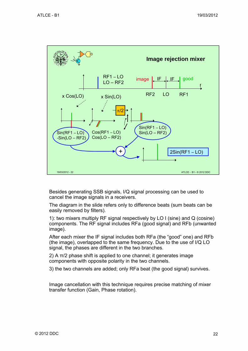
Image rejection mixer
2Sin(RF1 – LO)+
Sin(RF1 – LO)Sin(LO – RF2)
RF1 – LOLO – RF2
f
LORF2 RF1
IF IF
x Sin(LO)x Cos(LO)
image good
:
Sin(RF1 – LO)-Sin(LO – RF2)
Cos(RF1 – LO)Cos(LO – RF2)
/2
Besides generating SSB signals, I/Q signal processing can be used to cancel the image signals in a receivers.
The diagram in the slide refers only to difference beats (sum beats can be easily removed by filters).
1): two mixers multiply RF signal respectively by LO I (sine) and Q (cosine) components. The RF signal includes RFa (good signal) and RFb (unwanted image).
After each mixer the IF signal includes both RFa (the “good” one) and RFb(the image), overlapped to the same frequency. Due to the use of I/Q LO signal, the phases are different in the two branches.
2) A π/2 phase shift is applied to one channel; it generates image components with opposite polarity in the two channels.
3) the two channels are added; only RFa beat (the good signal) survives.
Image cancellation with this technique requires precise matching of mixer transfer function (Gain, Phase rotation).
ATLCE - B1 19/03/2012
© 2012 DDC 23
19/03/2012 - 23 ATLCE - B1 - © 2012 DDC
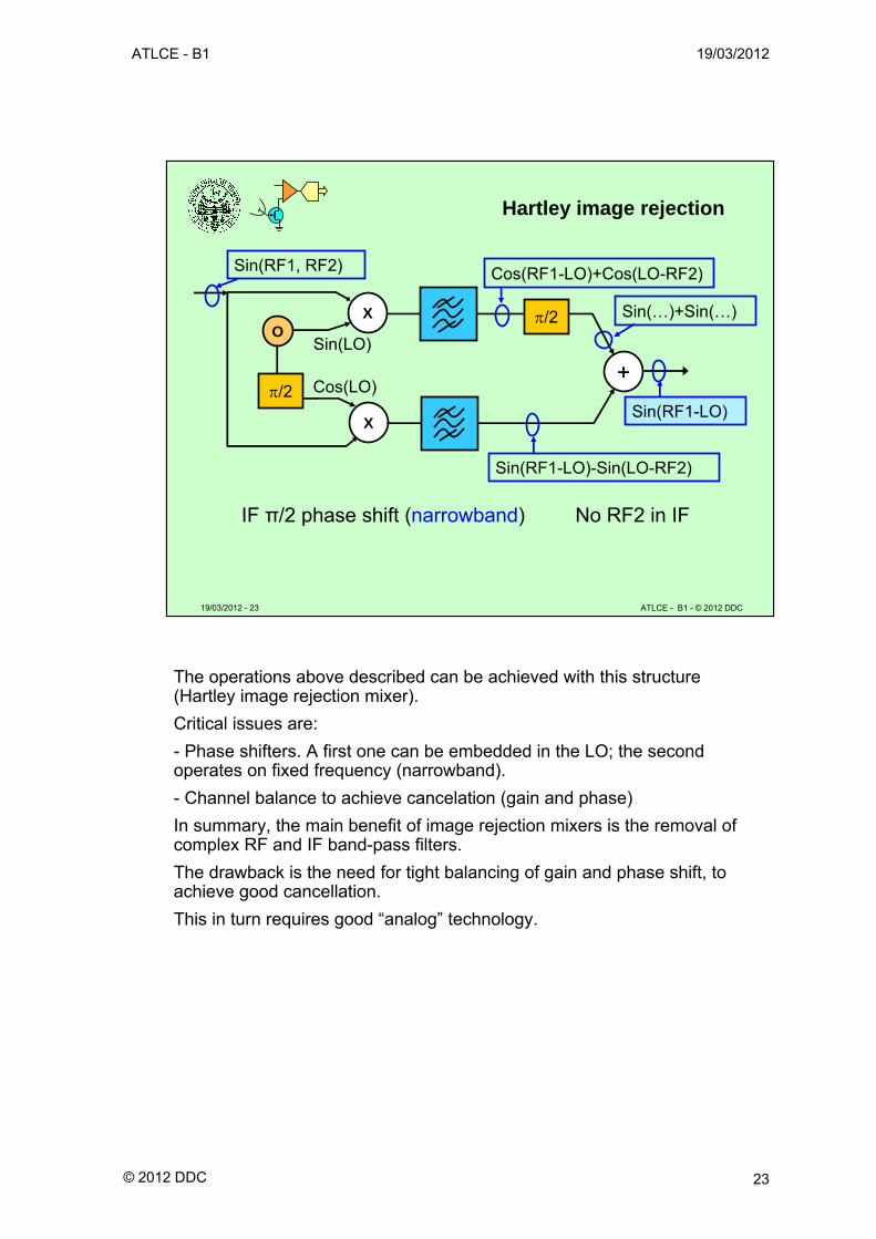
Hartley image rejection
IF π/2 phase shift (narrowband) No RF2 in IF
X
XO
/2+
/2
Sin(RF1, RF2)
Sin(LO)
Cos(LO)
Cos(RF1-LO)+Cos(LO-RF2)
Sin(RF1-LO)-Sin(LO-RF2)
Sin(…)+Sin(…)
Sin(RF1-LO)
:
-
The operations above described can be achieved with this structure (Hartley image rejection mixer).
Critical issues are:
- Phase shifters. A first one can be embedded in the LO; the second operates on fixed frequency (narrowband).
- Channel balance to achieve cancelation (gain and phase)
In summary, the main benefit of image rejection mixers is the removal of complex RF and IF band-pass filters.
The drawback is the need for tight balancing of gain and phase shift, to achieve good cancellation.
This in turn requires good “analog” technology.
ATLCE - B1 19/03/2012
© 2012 DDC 24
19/03/2012 - 24 ATLCE - B1 - © 2012 DDC
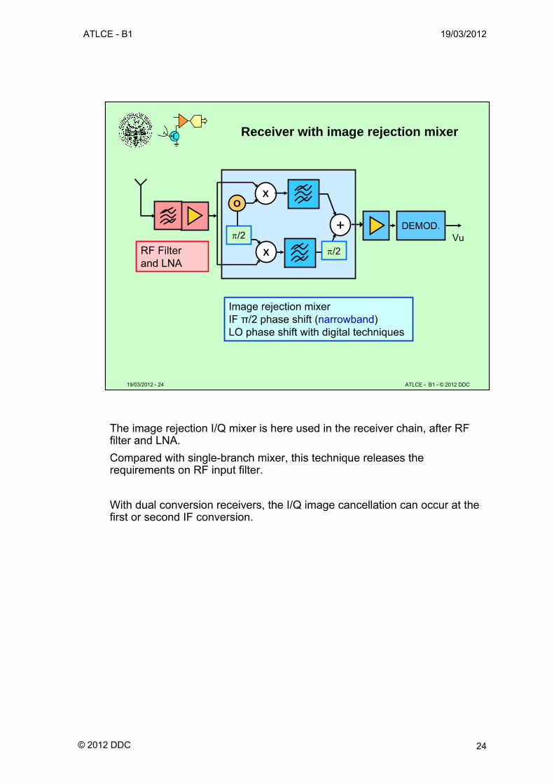
Receiver with image rejection mixer
Image rejection mixerIF π/2 phase shift (narrowband)LO phase shift with digital techniques
RF Filter and LNA
XO
/2DEMOD.
Vu+
/2X
The image rejection I/Q mixer is here used in the receiver chain, after RF filter and LNA.
Compared with single-branch mixer, this technique releases the requirements on RF input filter.
With dual conversion receivers, the I/Q image cancellation can occur at the first or second IF conversion.
ATLCE - B1 19/03/2012
© 2012 DDC 25
19/03/2012 - 25 ATLCE - B1 - © 2012 DDC
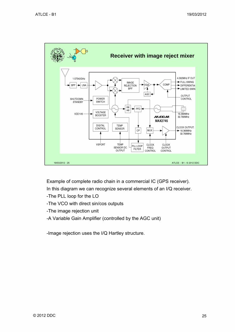
Receiver with image reject mixer
Example of complete radio chain in a commercial IC (GPS receiver).
In this diagram we can recognize several elements of an I/Q receiver.
-The PLL loop for the LO
-The VCO with direct sin/cos outputs
-The image rejection unit
-A Variable Gain Amplifier (controlled by the AGC unit)
-Image rejection uses the I/Q Hartley structure.
ATLCE - B1 19/03/2012
© 2012 DDC 26
19/03/2012 - 26 ATLCE - B1 - © 2012 DDC
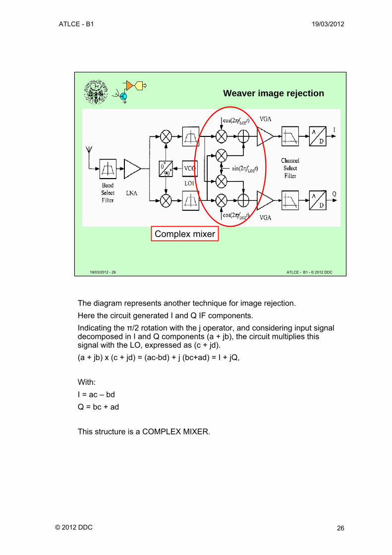
Weaver image rejection
Complex mixer
The diagram represents another technique for image rejection.
Here the circuit generated I and Q IF components.
Indicating the π/2 rotation with the j operator, and considering input signal decomposed in I and Q components (a + jb), the circuit multiplies this signal with the LO, expressed as (c + jd).
(a + jb) x (c + jd) = (ac-bd) + j (bc+ad) = I + jQ,
With:
I = ac – bd
Q = bc + ad
This structure is a COMPLEX MIXER.
ATLCE - B1 19/03/2012
© 2012 DDC 27
19/03/2012 - 27 ATLCE - B1 - © 2012 DDC
I-Q channels
I channelVI
X
XO
/2
VQ
Q channel
|V|
VaV
X
O1IF1Amplifier
DEM.
IF2Amplifier
:cos
sin
V
V
VI
VQ
tsenVV
tcosVV
I
Q
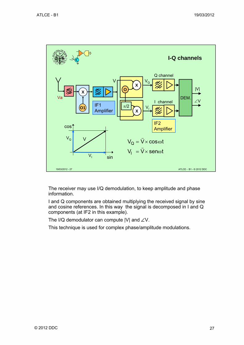
The receiver may use I/Q demodulation, to keep amplitude and phase information.
I and Q components are obtained multiplying the received signal by sine and cosine references. In this way the signal is decomposed in I and Q components (at IF2 in this example).
The I/Q demodulator can compute |V| and V.
This technique is used for complex phase/amplitude modulations.
ATLCE - B1 19/03/2012
© 2012 DDC 28
19/03/2012 - 28 ATLCE - B1 - © 2012 DDC
Zero- IF (or low-IF) receiver
Received signal at fa directly moved to baseband
Lowpass filter in IF channel
Input filter and LNA(variable F)
XO
DEMOD.Va
Vu
Low pass filter
f
fO = fa1fi = 0
fa
fO
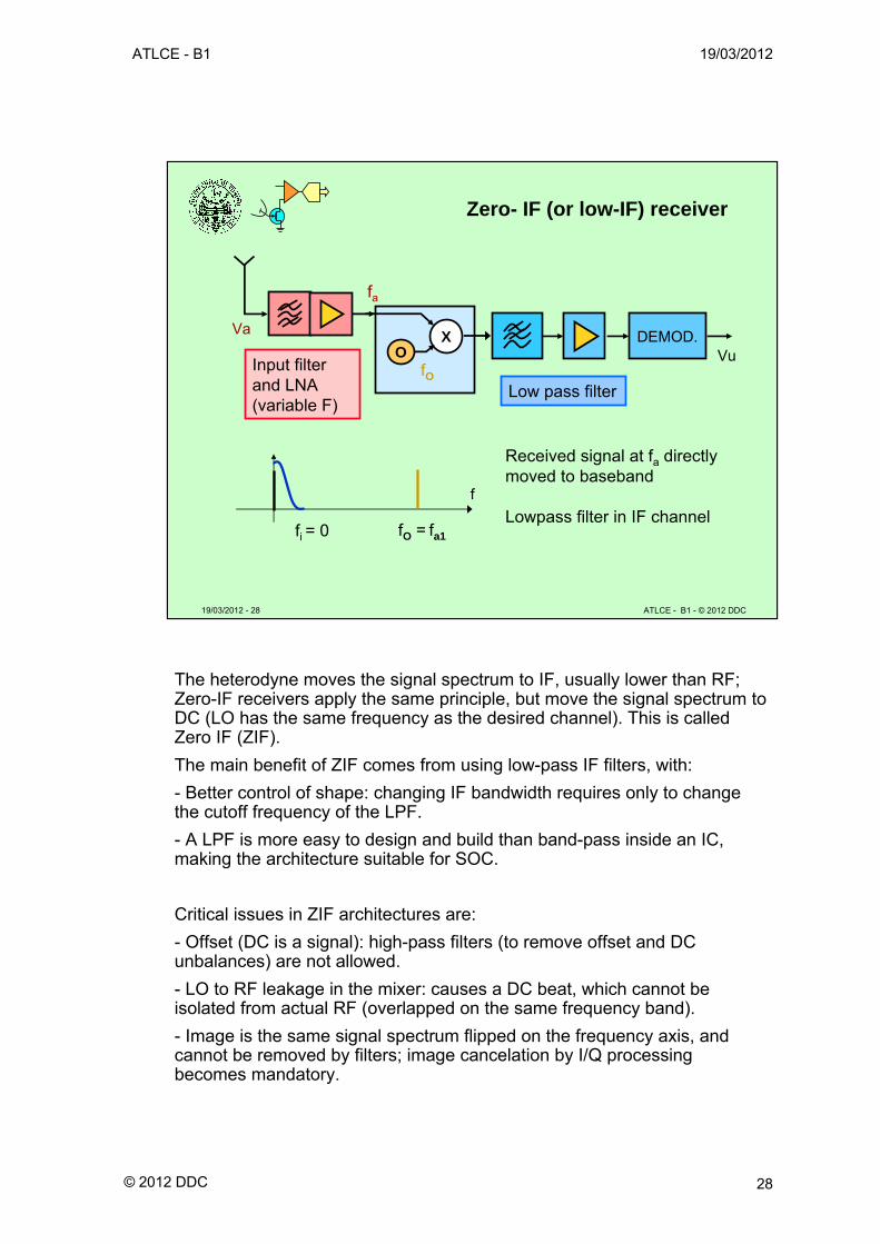
The heterodyne moves the signal spectrum to IF, usually lower than RF; Zero-IF receivers apply the same principle, but move the signal spectrum to DC (LO has the same frequency as the desired channel). This is called Zero IF (ZIF).
The main benefit of ZIF comes from using low-pass IF filters, with:
- Better control of shape: changing IF bandwidth requires only to change the cutoff frequency of the LPF.
- A LPF is more easy to design and build than band-pass inside an IC, making the architecture suitable for SOC.
Critical issues in ZIF architectures are:
- Offset (DC is a signal): high-pass filters (to remove offset and DC unbalances) are not allowed.
- LO to RF leakage in the mixer: causes a DC beat, which cannot be isolated from actual RF (overlapped on the same frequency band).
- Image is the same signal spectrum flipped on the frequency axis, and cannot be removed by filters; image cancelation by I/Q processing becomes mandatory.
ATLCE - B1 19/03/2012
© 2012 DDC 29
19/03/2012 - 29 ATLCE - B1 - © 2012 DDC
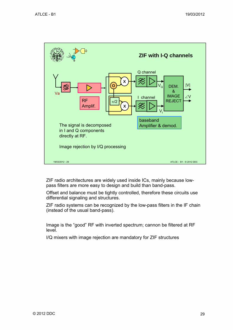
ZIF with I-Q channels
The signal is decomposed in I and Q components directly at RF.
Image rejection by I/Q processing
I channel
VI
X
XO
/2
VQ
Q channel
|V|
VaV
RFAmplif.
DEM.&
IMAGEREJECT
basebandAmplifier & demod.
ZIF radio architectures are widely used inside ICs, mainly because low-pass filters are more easy to design and build than band-pass.
Offset and balance must be tightly controlled, therefore these circuits use differential signaling and structures.
ZIF radio systems can be recognized by the low-pass filters in the IF chain (instead of the usual band-pass).
Image is the “good” RF with inverted spectrum; cannon be filtered at RF level.
I/Q mixers with image rejection are mandatory for ZIF structures
ATLCE - B1 19/03/2012
© 2012 DDC 30
19/03/2012 - 30 ATLCE - B1 - © 2012 DDC
ZIF benefits an problems
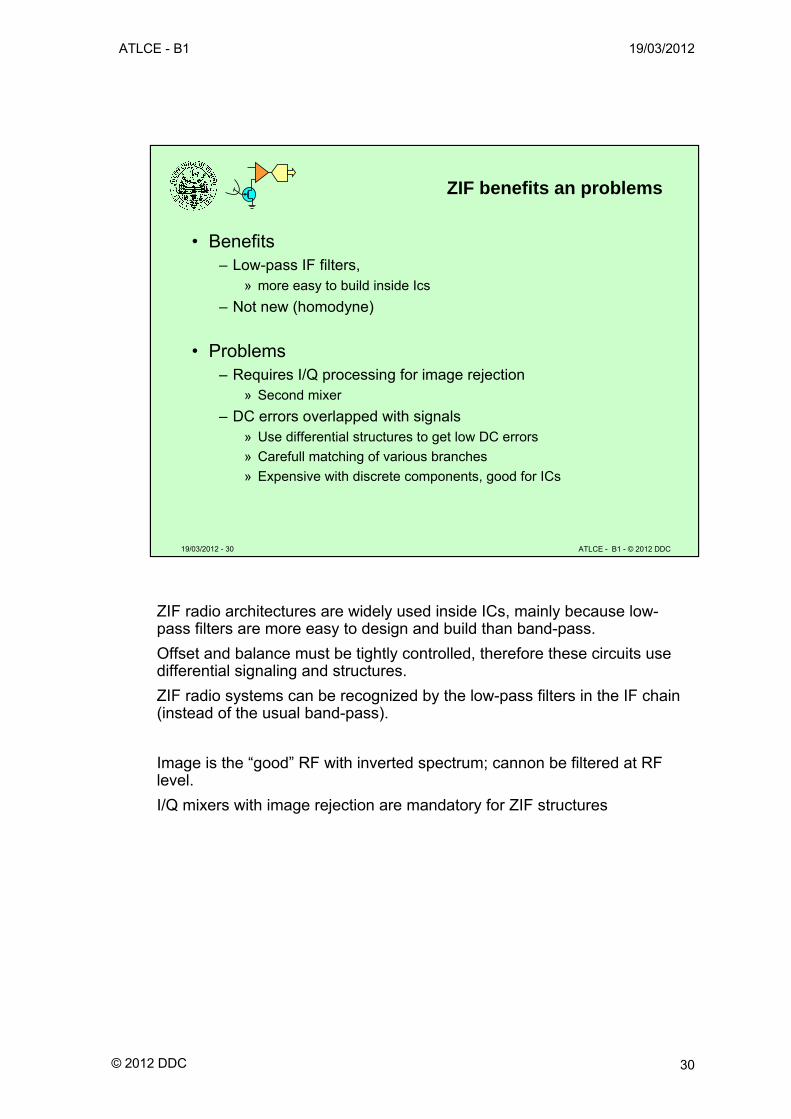
• Benefits– Low-pass IF filters,
» more easy to build inside Ics
– Not new (homodyne)
• Problems– Requires I/Q processing for image rejection
» Second mixer
– DC errors overlapped with signals» Use differential structures to get low DC errors
» Carefull matching of various branches
» Expensive with discrete components, good for ICs
ZIF radio architectures are widely used inside ICs, mainly because low-pass filters are more easy to design and build than band-pass.
Offset and balance must be tightly controlled, therefore these circuits use differential signaling and structures.
ZIF radio systems can be recognized by the low-pass filters in the IF chain (instead of the usual band-pass).
Image is the “good” RF with inverted spectrum; cannon be filtered at RF level.
I/Q mixers with image rejection are mandatory for ZIF structures
ATLCE - B1 19/03/2012
© 2012 DDC 31
19/03/2012 - 31 ATLCE - B1 - © 2012 DDC
Example of ZIF with I-Q channels
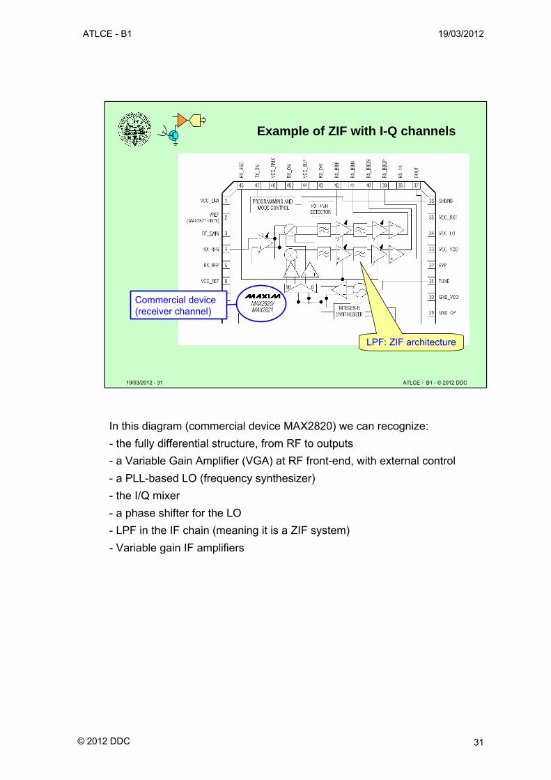
Commercial device(receiver channel)
LPF: ZIF architecture
In this diagram (commercial device MAX2820) we can recognize:
- the fully differential structure, from RF to outputs
- a Variable Gain Amplifier (VGA) at RF front-end, with external control
- a PLL-based LO (frequency synthesizer)
- the I/Q mixer
- a phase shifter for the LO
- LPF in the IF chain (meaning it is a ZIF system)
- Variable gain IF amplifiers
ATLCE - B1 19/03/2012
© 2012 DDC 32
19/03/2012 - 32 ATLCE - B1 - © 2012 DDC
Lesson B1: radio system architectures
• Heterodyne receivers
• The image problem
• Dual conversion receivers
• Complex mixer & I/Q processing
• Digital receivers
• Software Defined Radio
• Examples
All the system previously analyzed are based on analog building blocks (filters, amplifiers, mixer, local oscillator).
The same function can be obtained also with digital circuits, which give benefits in terms of design ease, fabrication cost, and flexibility.
Moving from analog to Digital requires an Analog-to-Digital converter (ADC) somewhere along the receiver chain. The ADC position defines theboundary between analog and digital processing: all units before the ADC operate on analog signals, the ones after it process digital samples.
The various positions correspond to different tradeoff between complexity, performance, power consumption. This section describes the various choices for moving from the analog structures to digital ones, discussing the respective benefit and drawbacks.
ATLCE - B1 19/03/2012
© 2012 DDC 33
19/03/2012 - 33 ATLCE - B1 - © 2012 DDC
First step towards digital radio
Many applications use directly digital data
XO
Va
out
Analog Demodulator
DEMOD. A/D
IF channel
Wideband filter
IF filter and Amplifier (fixed F)
A/D conversion after demodulation.
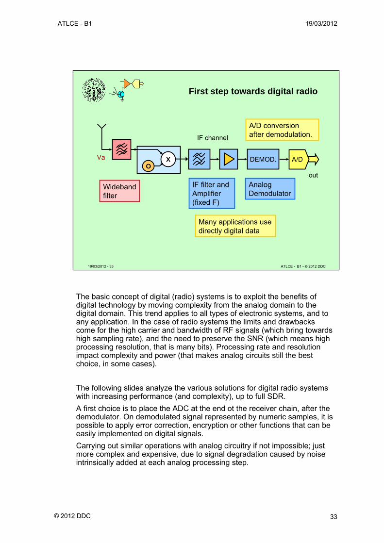
The basic concept of digital (radio) systems is to exploit the benefits of digital technology by moving complexity from the analog domain to the digital domain. This trend applies to all types of electronic systems, and to any application. In the case of radio systems the limits and drawbacks come for the high carrier and bandwidth of RF signals (which bring towards high sampling rate), and the need to preserve the SNR (which means high processing resolution, that is many bits). Processing rate and resolution impact complexity and power (that makes analog circuits still the best choice, in some cases).
The following slides analyze the various solutions for digital radio systems with increasing performance (and complexity), up to full SDR.
A first choice is to place the ADC at the end ot the receiver chain, after the demodulator. On demodulated signal represented by numeric samples, it is possible to apply error correction, encryption or other functions that can be easily implemented on digital signals.
Carrying out similar operations with analog circuitry if not impossible; just more complex and expensive, due to signal degradation caused by noise intrinsically added at each analog processing step.
ATLCE - B1 19/03/2012
© 2012 DDC 34
19/03/2012 - 34 ATLCE - B1 - © 2012 DDC
More digital - 2
The digital demodulator can use complex algorithmsThe same HW support different types of modulationThe A/D converter must operate at high frequency
XO
Va
VuA/D
Digital demodulator
DEMOD.
IF channel
IF filter and Amplifier (fixed F)
Wideband filter
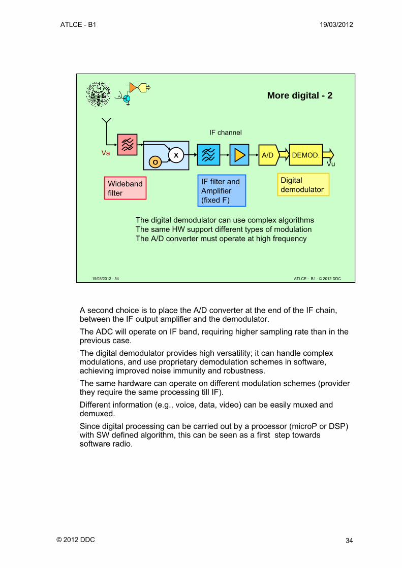
A second choice is to place the A/D converter at the end of the IF chain, between the IF output amplifier and the demodulator.
The ADC will operate on IF band, requiring higher sampling rate than in the previous case.
The digital demodulator provides high versatility; it can handle complex modulations, and use proprietary demodulation schemes in software, achieving improved noise immunity and robustness.
The same hardware can operate on different modulation schemes (provider they require the same processing till IF).
Different information (e.g., voice, data, video) can be easily muxed and demuxed.
Since digital processing can be carried out by a processor (microP or DSP) with SW defined algorithm, this can be seen as a first step towards software radio.
ATLCE - B1 19/03/2012
© 2012 DDC 35
19/03/2012 - 35 ATLCE - B1 - © 2012 DDC
More digital - 3
XO
IF (digital) channel
Vu
A/D
IF filter and demodulator (all digital)
DEMOD.Va
Wideban LNA and filter (variable F)
The digital IF filter increases the computational load, but allows to modify the IF parameters in the SW
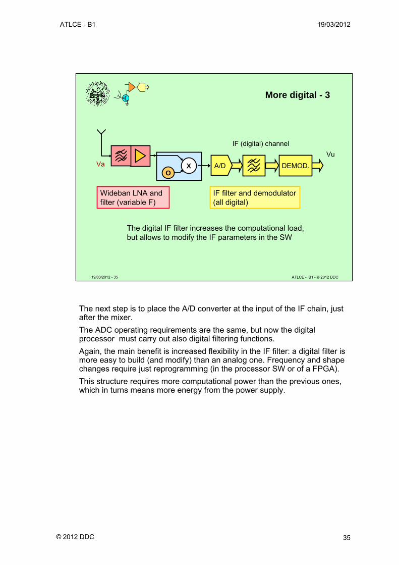
The next step is to place the A/D converter at the input of the IF chain, just after the mixer.
The ADC operating requirements are the same, but now the digitalprocessor must carry out also digital filtering functions.
Again, the main benefit is increased flexibility in the IF filter: a digital filter is more easy to build (and modify) than an analog one. Frequency and shape changes require just reprogramming (in the processor SW or of a FPGA).
This structure requires more computational power than the previous ones, which in turns means more energy from the power supply.
ATLCE - B1 19/03/2012
© 2012 DDC 36
19/03/2012 - 36 ATLCE - B1 - © 2012 DDC
Mixing and sampling
Sampling can be seen as product of the signal with a sequence of δ.
The spectrum of a δ is a sequence of δ
The product of input signal with the fundamental frequency of the δ stream corresponds to the mixing operation
A mixer shifts the input signal frequency
O
DEMOD.A/DVa
XO
Local oscillator
S/H
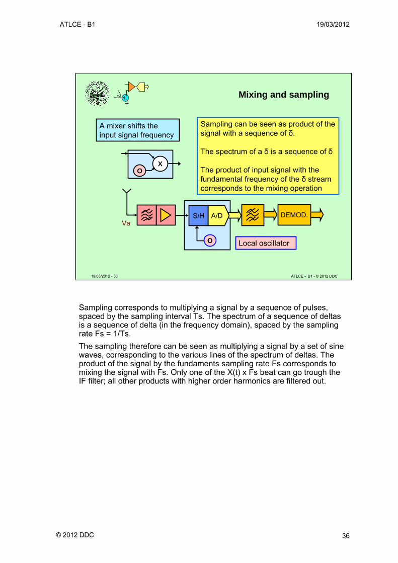
Sampling corresponds to multiplying a signal by a sequence of pulses, spaced by the sampling interval Ts. The spectrum of a sequence of deltas is a sequence of delta (in the frequency domain), spaced by the sampling rate Fs = 1/Ts.
The sampling therefore can be seen as multiplying a signal by a set of sine waves, corresponding to the various lines of the spectrum of deltas. The product of the signal by the fundaments sampling rate Fs corresponds to mixing the signal with Fs. Only one of the X(t) x Fs beat can go trough the IF filter; all other products with higher order harmonics are filtered out.
ATLCE - B1 19/03/2012
© 2012 DDC 37
19/03/2012 - 37 ATLCE - B1 - © 2012 DDC
Heterodyne frequency translation
f
f
f
LO1
IF bandpass filter
RF signal
B1
LocalOscillatorLO1
Difference beat:IF signal
B1
Sum beat
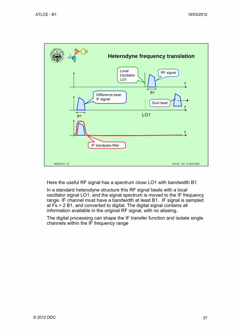
Here the useful RF signal has a spectrum close LO1 with bandwidth B1.
In a standard heterodyne structure this RF signal beats with a local oscillator signal LO1, and the signal spectrum is moved to the IF frequency range. IF channel must have a bandwidth at least B1. IF signal is sampled at Fs > 2 B1, and converted to digital. The digital signal contains all information available in the original RF signal, with no aliasing.
The digital processing can shape the IF transfer function and isolate single channels within the IF frequency range
ATLCE - B1 19/03/2012
© 2012 DDC 38
19/03/2012 - 38 ATLCE - B1 - © 2012 DDC
Nyquist sampling and reconstruction
f
f
FS 4FS
FS = 1/TS
f
FS 2FS 4FS3FS
Sampling rate
Anti-aliasing input filter
SignalSpectrum S
Anti-aliasing reconstruction (output) filterAliases caused by sampling
S
FS - S FS + S
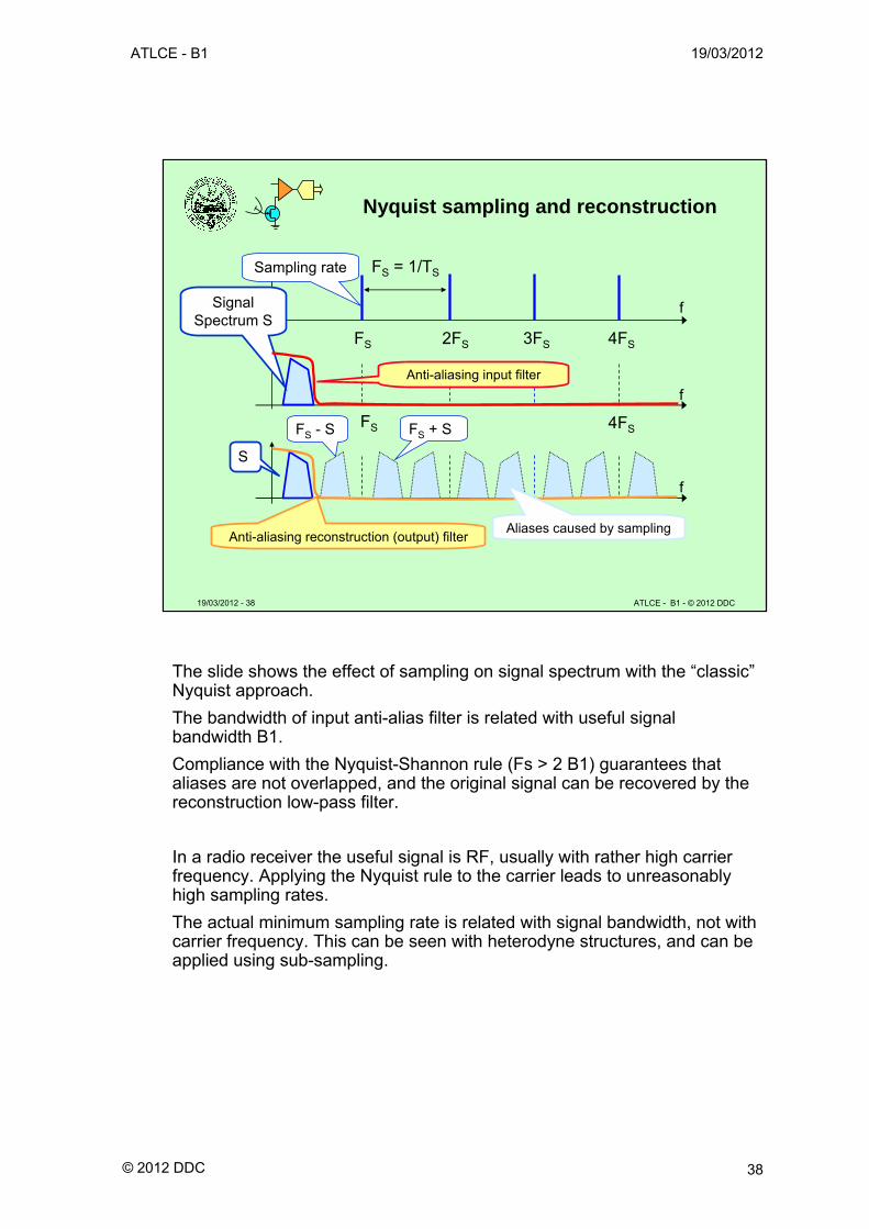
The slide shows the effect of sampling on signal spectrum with the “classic”Nyquist approach.
The bandwidth of input anti-alias filter is related with useful signal bandwidth B1.
Compliance with the Nyquist-Shannon rule (Fs > 2 B1) guarantees that aliases are not overlapped, and the original signal can be recovered by the reconstruction low-pass filter.
In a radio receiver the useful signal is RF, usually with rather high carrier frequency. Applying the Nyquist rule to the carrier leads to unreasonably high sampling rates.
The actual minimum sampling rate is related with signal bandwidth, not with carrier frequency. This can be seen with heterodyne structures, and can be applied using sub-sampling.
ATLCE - B1 19/03/2012
© 2012 DDC 39
19/03/2012 - 39 ATLCE - B1 - © 2012 DDC
Frequency translation by sampling
f
f
f
FS2FS 4FS3FS
Reconstruction filter
Sampling rate RF signal S
> 2 B1
Sampled signal
5FS - S S - FSS - 3FS S
B1
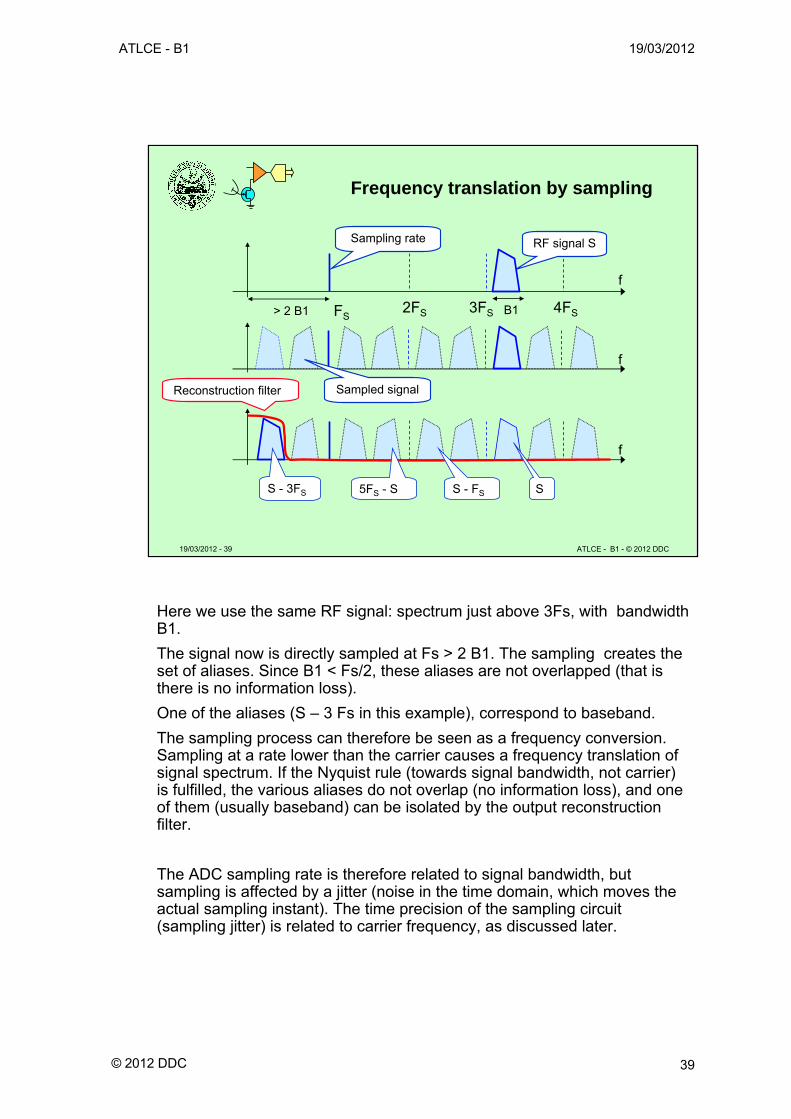
Here we use the same RF signal: spectrum just above 3Fs, with bandwidth B1.
The signal now is directly sampled at Fs > 2 B1. The sampling creates the set of aliases. Since B1 < Fs/2, these aliases are not overlapped (that is there is no information loss).
One of the aliases (S – 3 Fs in this example), correspond to baseband.
The sampling process can therefore be seen as a frequency conversion. Sampling at a rate lower than the carrier causes a frequency translation of signal spectrum. If the Nyquist rule (towards signal bandwidth, not carrier) is fulfilled, the various aliases do not overlap (no information loss), and one of them (usually baseband) can be isolated by the output reconstruction filter.
The ADC sampling rate is therefore related to signal bandwidth, but sampling is affected by a jitter (noise in the time domain, which moves the actual sampling instant). The time precision of the sampling circuit (sampling jitter) is related to carrier frequency, as discussed later.
ATLCE - B1 19/03/2012
© 2012 DDC 40
19/03/2012 - 40 ATLCE - B1 - © 2012 DDC
Subsampling and spectrum folding
FS = 1/TS
f
f
f
FS 2FS 4FS3FS
S
5FS - S S - FSS - 3FS
Sampling rate
RF signal
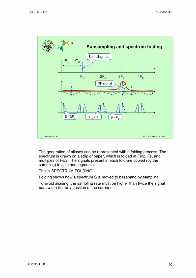
The generation of aliases can be represented with a folding process. The spectrum is drawn on a strip of paper, which is folded at Fs/2, Fs, and multiples of Fs/2. The signals present in each fold are copied (by the sampling) to all other segments.
This is SPECTRUM FOLDING.
Folding shows how a spectrum S is moved to baseband by sampling.
To avoid aliasing, the sampling rate must be higher than twice the signal bandwidth (for any position of the carrier).
ATLCE - B1 19/03/2012
© 2012 DDC 41
19/03/2012 - 41 ATLCE - B1 - © 2012 DDC
Single signal subsampling and folding
FS 2FS0
FS/2 3FS/2
FS
2FS
0FS/2
3FS/2
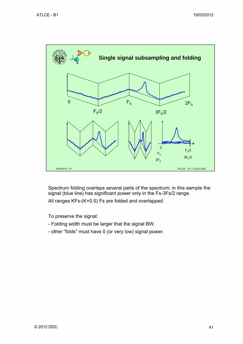
Spectrum folding overlaps several parts of the spectrum; in this eample the signal (blue line) has significant power only in the Fs-3Fs/2 range.
All ranges KFs-(K+0.5) Fs are folded and overlapped.
To preserve the signal:
- Folding width must be larger that the signal BW.
- other “folds” must have 0 (or very low) signal power.
ATLCE - B1 19/03/2012
© 2012 DDC 42
19/03/2012 - 42 ATLCE - B1 - © 2012 DDC
Subsampling and folding
From: Critical techniques for High Speed A/D converters - Pentek
RF filterUnwantedOut-of-Band
Signals
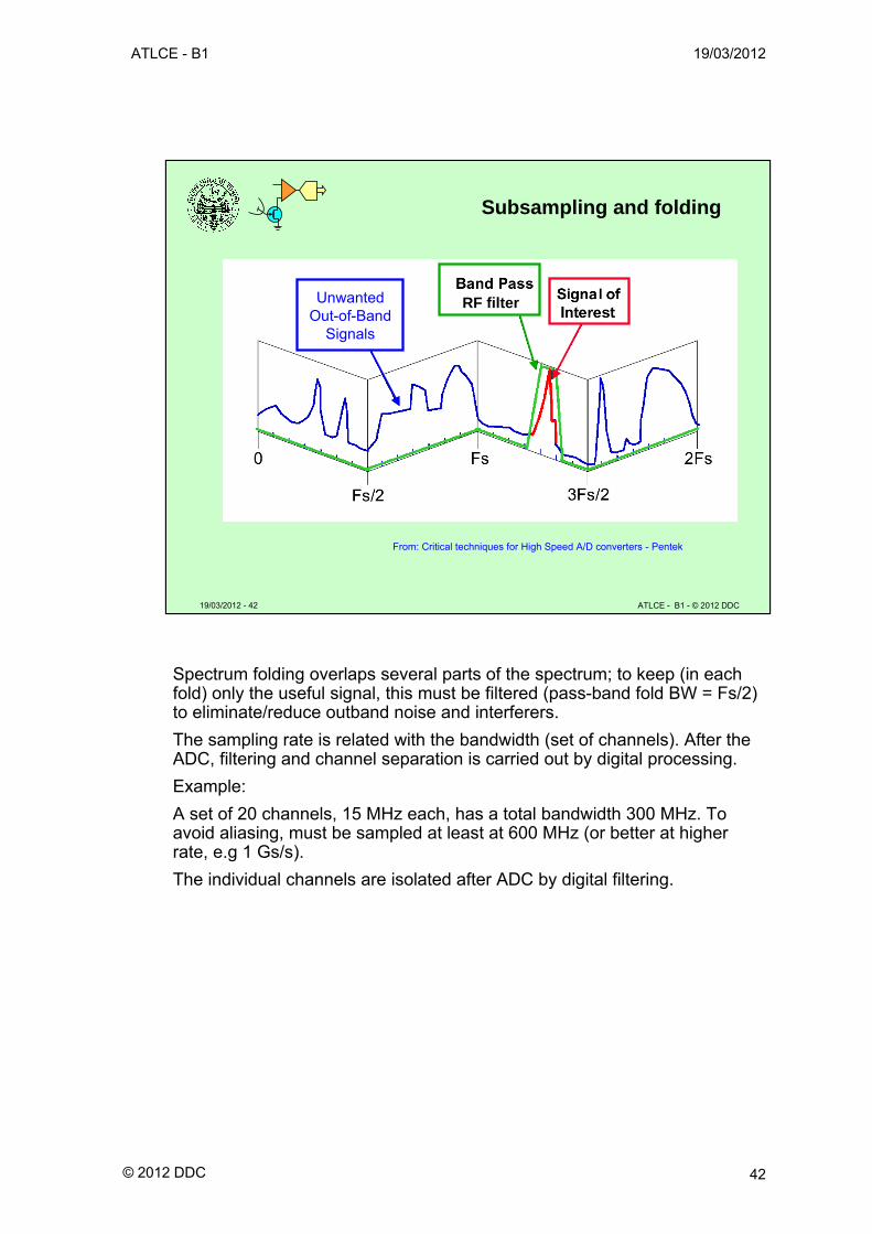
Spectrum folding overlaps several parts of the spectrum; to keep (in each fold) only the useful signal, this must be filtered (pass-band fold BW = Fs/2) to eliminate/reduce outband noise and interferers.
The sampling rate is related with the bandwidth (set of channels). After the ADC, filtering and channel separation is carried out by digital processing.
Example:
A set of 20 channels, 15 MHz each, has a total bandwidth 300 MHz. To avoid aliasing, must be sampled at least at 600 MHz (or better at higher rate, e.g 1 Gs/s).
The individual channels are isolated after ADC by digital filtering.
ATLCE - B1 19/03/2012
© 2012 DDC 43
19/03/2012 - 43 ATLCE - B1 - © 2012 DDC
Folding with spurious and noise
FS = 1/TS
f
f
FS 2FS 4FS3FS
Sampling rate
Outband spuriousand noise
Useful signal
f
Folding overlaps spurious and noise in baseband UNUSABLE !
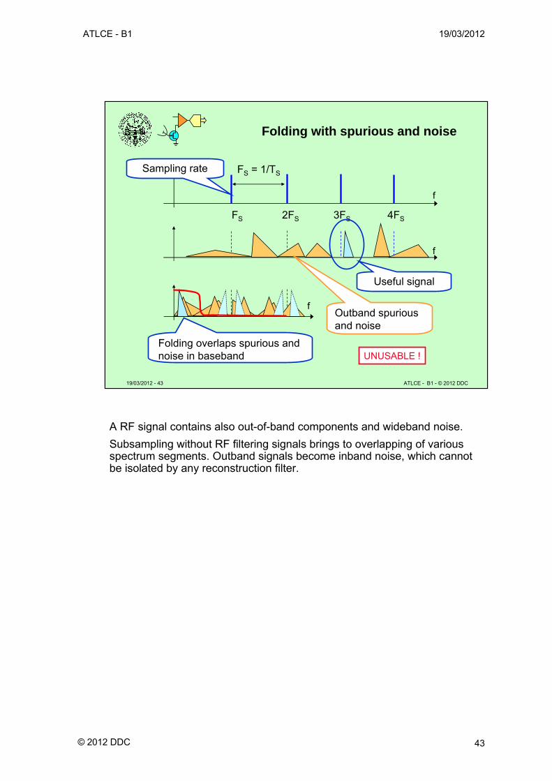
A RF signal contains also out-of-band components and wideband noise.
Subsampling without RF filtering signals brings to overlapping of various spectrum segments. Outband signals become inband noise, which cannot be isolated by any reconstruction filter.
ATLCE - B1 19/03/2012
© 2012 DDC 44
19/03/2012 - 44 ATLCE - B1 - © 2012 DDC
Subsampling and filtering
FS = 1/TS
f
f
f
FS 2FS 4FS3FS
Translated signal Lowpass filter
Bandpass filter
Useful signal
OK
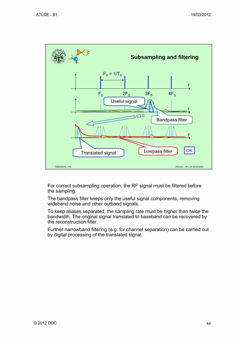
For correct subsampling operation, the RF signal must be filtered before the sampling.
The bandpass filter keeps only the useful signal components, removing wideband noise and other outband signals.
To keep aliases separated, the sampling rate must be higher than twice the bandwidth. The original signal translated to baseband can be recovered by the reconstruction filter.
Further narrowband filtering (e.g. for channel separation) can be carried out by digital processing of the translated signal.
ATLCE - B1 19/03/2012
© 2012 DDC 45
19/03/2012 - 45 ATLCE - B1 - © 2012 DDC
Which sampling rate?
f
Sampling rateMultichannel RF signal
FS 2FS 3FS> 2 B1
Baseband signal (still multichannel)
Feasible RF filter
Too narrow filter
f
f
Channel filter (Digital)
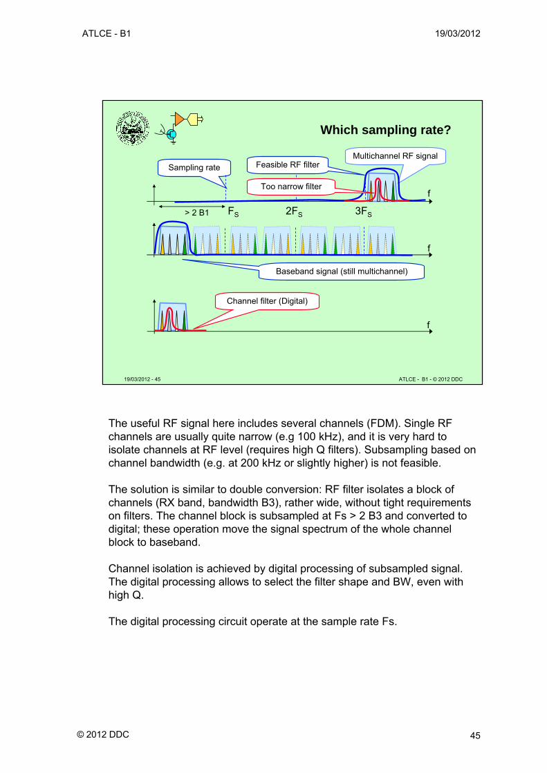
The useful RF signal here includes several channels (FDM). Single RF channels are usually quite narrow (e.g 100 kHz), and it is very hard to isolate channels at RF level (requires high Q filters). Subsampling based on channel bandwidth (e.g. at 200 kHz or slightly higher) is not feasible.
The solution is similar to double conversion: RF filter isolates a block of channels (RX band, bandwidth B3), rather wide, without tight requirements on filters. The channel block is subsampled at Fs > 2 B3 and converted to digital; these operation move the signal spectrum of the whole channel block to baseband.
Channel isolation is achieved by digital processing of subsampled signal. The digital processing allows to select the filter shape and BW, even with high Q.
The digital processing circuit operate at the sample rate Fs.
ATLCE - B1 19/03/2012
© 2012 DDC 46
19/03/2012 - 46 ATLCE - B1 - © 2012 DDC
Subsampling and sampling jitter
• Sampling rate depends on signal bandwidth– Subsampling receivers use less power
• Sampling jitter depends on carrier– Amplitude error = (time jitter) x (slew rate)
Slew rate = V x ω(carrier)
– Phase error in I/Q chains
• Sampling jitter is a critical parameter
• Need for – low jitter sampling clock
– high-speed Sample/Hold circuits (low aperture jitter)
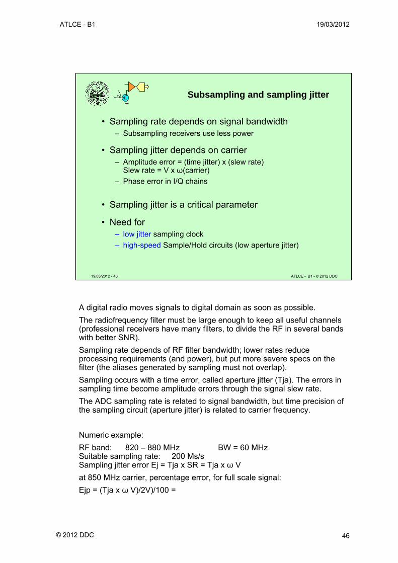
A digital radio moves signals to digital domain as soon as possible.
The radiofrequency filter must be large enough to keep all useful channels (professional receivers have many filters, to divide the RF in several bands with better SNR).
Sampling rate depends of RF filter bandwidth; lower rates reduceprocessing requirements (and power), but put more severe specs on the filter (the aliases generated by sampling must not overlap).
Sampling occurs with a time error, called aperture jitter (Tja). The errors in sampling time become amplitude errors through the signal slew rate.
The ADC sampling rate is related to signal bandwidth, but time precision of the sampling circuit (aperture jitter) is related to carrier frequency.
Numeric example:
RF band: 820 – 880 MHz BW = 60 MHzSuitable sampling rate: 200 Ms/sSampling jitter error Ej = Tja x SR = Tja x ω V
at 850 MHz carrier, percentage error, for full scale signal:
Ejp = (Tja x ω V)/2V)/100 =
ATLCE - B1 19/03/2012
© 2012 DDC 47
19/03/2012 - 47 ATLCE - B1 - © 2012 DDC
Oversampling, filtering and decimation
A:Complete input signal
Filtering, resampling at lower rate …
ffs
ffs
other spectral components (useless)
signal of interest
f ’
Nyquist rate
2f ’
f
… and decimate (get rid of redundant samples)
fs f ’
B:Usefulinput signal
C:Signal after decimation
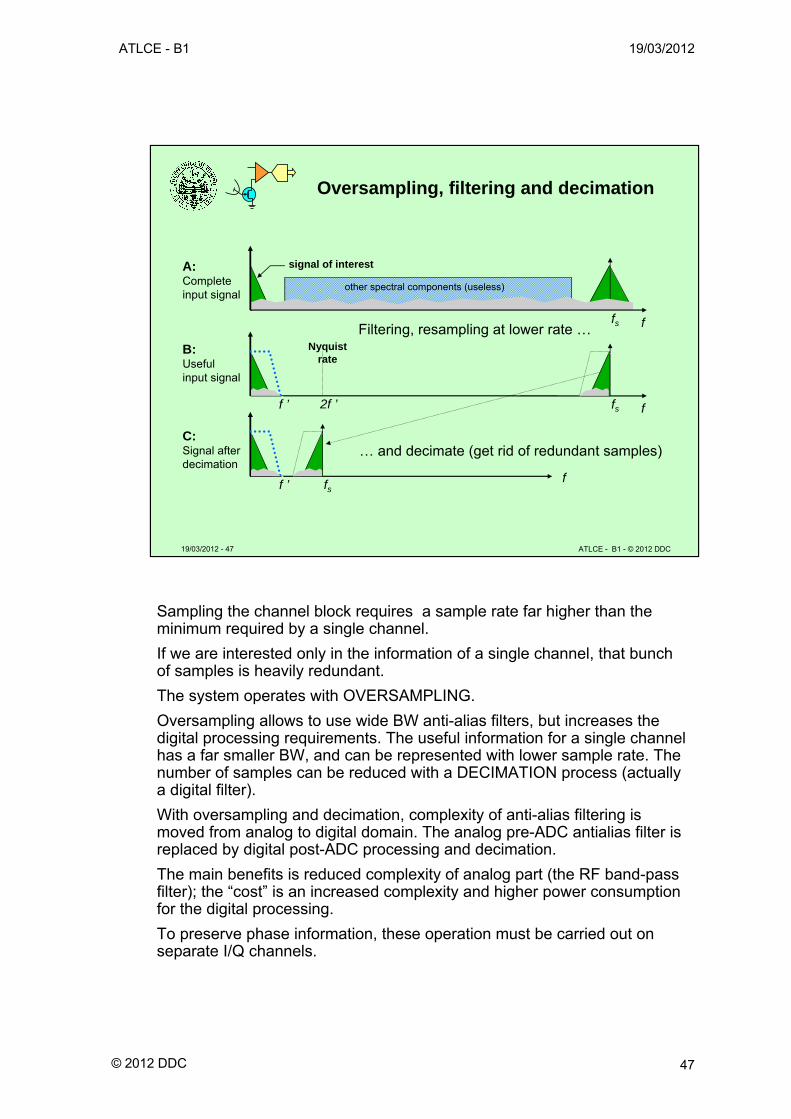
Sampling the channel block requires a sample rate far higher than the minimum required by a single channel.
If we are interested only in the information of a single channel, that bunch of samples is heavily redundant.
The system operates with OVERSAMPLING.
Oversampling allows to use wide BW anti-alias filters, but increases the digital processing requirements. The useful information for a single channel has a far smaller BW, and can be represented with lower sample rate. The number of samples can be reduced with a DECIMATION process (actually a digital filter).
With oversampling and decimation, complexity of anti-alias filtering is moved from analog to digital domain. The analog pre-ADC antialias filter is replaced by digital post-ADC processing and decimation.
The main benefits is reduced complexity of analog part (the RF band-pass filter); the “cost” is an increased complexity and higher power consumption for the digital processing.
To preserve phase information, these operation must be carried out on separate I/Q channels.
ATLCE - B1 19/03/2012
© 2012 DDC 48
19/03/2012 - 48 ATLCE - B1 - © 2012 DDC
Digital downconversion (GSM receiver)
A BC
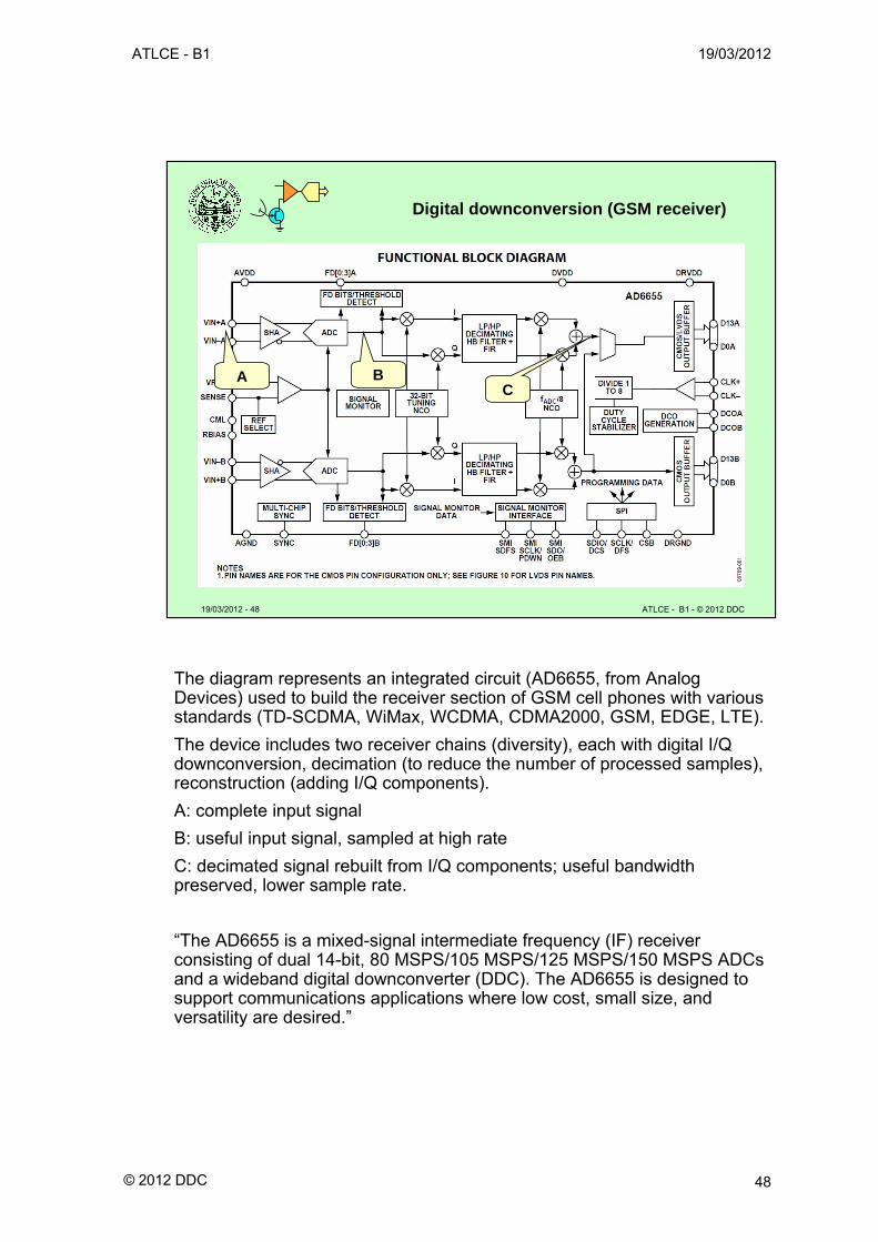
The diagram represents an integrated circuit (AD6655, from Analog Devices) used to build the receiver section of GSM cell phones with various standards (TD-SCDMA, WiMax, WCDMA, CDMA2000, GSM, EDGE, LTE).
The device includes two receiver chains (diversity), each with digital I/Q downconversion, decimation (to reduce the number of processed samples), reconstruction (adding I/Q components).
A: complete input signal
B: useful input signal, sampled at high rate
C: decimated signal rebuilt from I/Q components; useful bandwidth preserved, lower sample rate.
“The AD6655 is a mixed-signal intermediate frequency (IF) receiver consisting of dual 14-bit, 80 MSPS/105 MSPS/125 MSPS/150 MSPS ADCs and a wideband digital downconverter (DDC). The AD6655 is designed to support communications applications where low cost, small size, and versatility are desired.”
ATLCE - B1 19/03/2012
© 2012 DDC 49
19/03/2012 - 49 ATLCE - B1 - © 2012 DDC
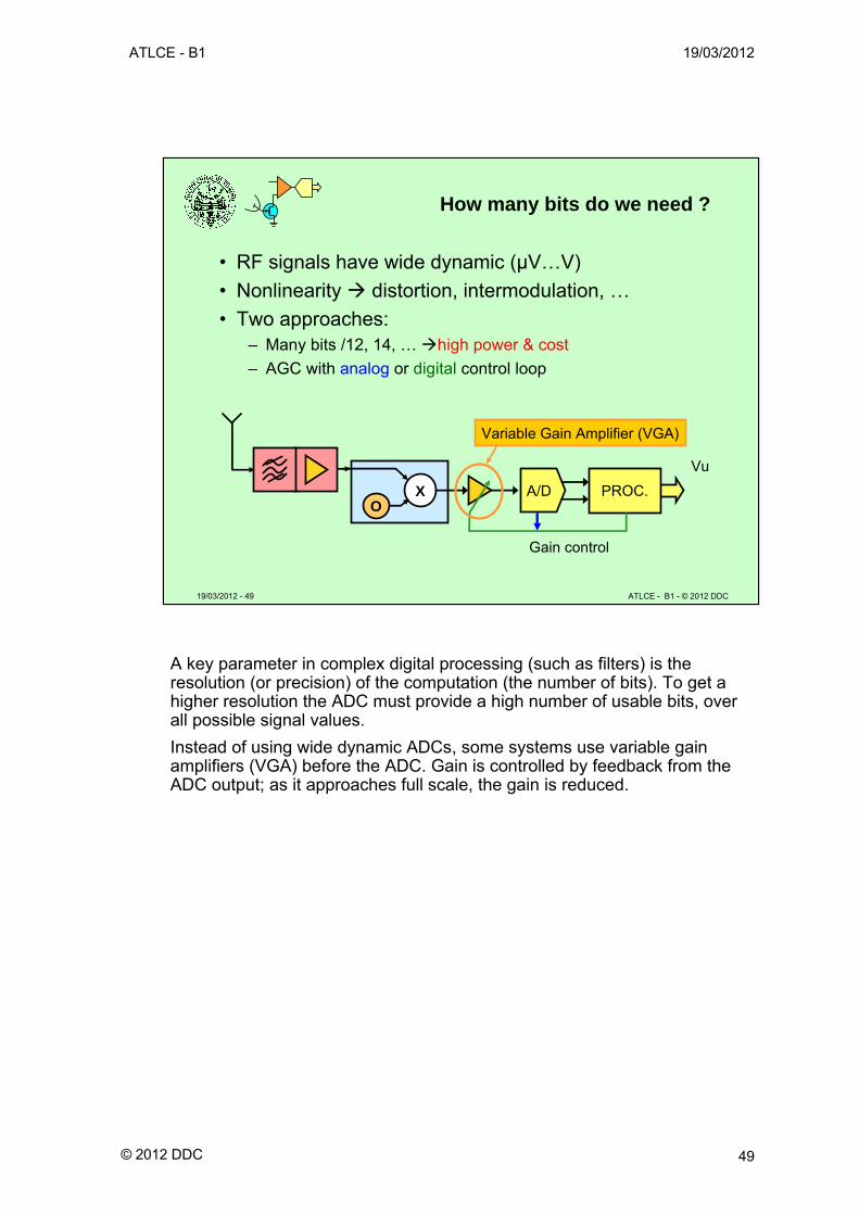
How many bits do we need ?
• RF signals have wide dynamic (µV…V)
• Nonlinearity distortion, intermodulation, …
• Two approaches:– Many bits /12, 14, …high power & cost
– AGC with analog or digital control loop
XO
Gain control
Vu
A/D PROC.
Variable Gain Amplifier (VGA)
A key parameter in complex digital processing (such as filters) is the resolution (or precision) of the computation (the number of bits). To get a higher resolution the ADC must provide a high number of usable bits, over all possible signal values.
Instead of using wide dynamic ADCs, some systems use variable gain amplifiers (VGA) before the ADC. Gain is controlled by feedback from the ADC output; as it approaches full scale, the gain is reduced.
ATLCE - B1 19/03/2012
© 2012 DDC 50
19/03/2012 - 50 ATLCE - B1 - © 2012 DDC
μP, DSP
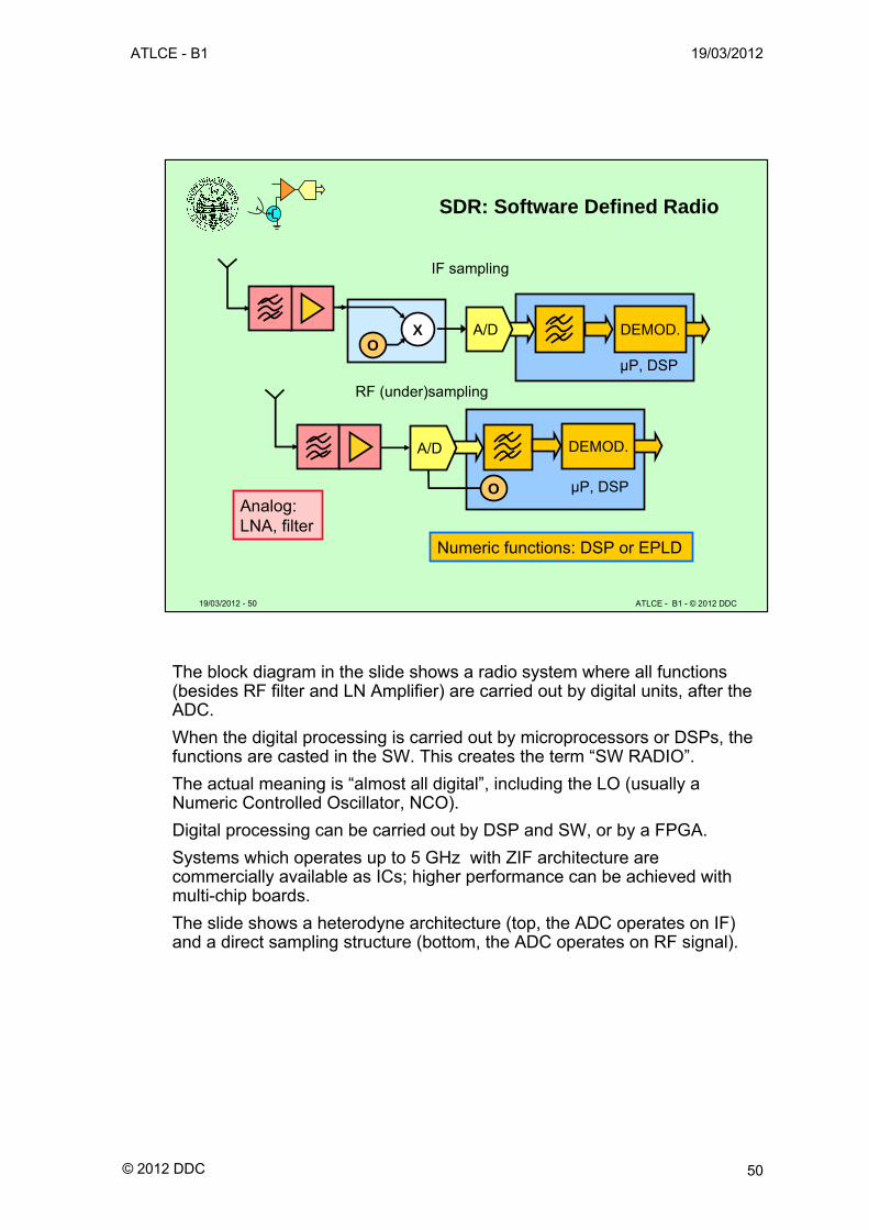
SDR: Software Defined Radio
Numeric functions: DSP or EPLD
μP, DSP O
DEMOD.A/D
Analog:LNA, filter
XO
IF sampling
A/D DEMOD.
RF (under)sampling
The block diagram in the slide shows a radio system where all functions (besides RF filter and LN Amplifier) are carried out by digital units, after the ADC.
When the digital processing is carried out by microprocessors or DSPs, the functions are casted in the SW. This creates the term “SW RADIO”.
The actual meaning is “almost all digital”, including the LO (usually a Numeric Controlled Oscillator, NCO).
Digital processing can be carried out by DSP and SW, or by a FPGA.
Systems which operates up to 5 GHz with ZIF architecture are commercially available as ICs; higher performance can be achieved with multi-chip boards.
The slide shows a heterodyne architecture (top, the ADC operates on IF) and a direct sampling structure (bottom, the ADC operates on RF signal).
ATLCE - B1 19/03/2012
© 2012 DDC 51
19/03/2012 - 51 ATLCE - B1 - © 2012 DDC
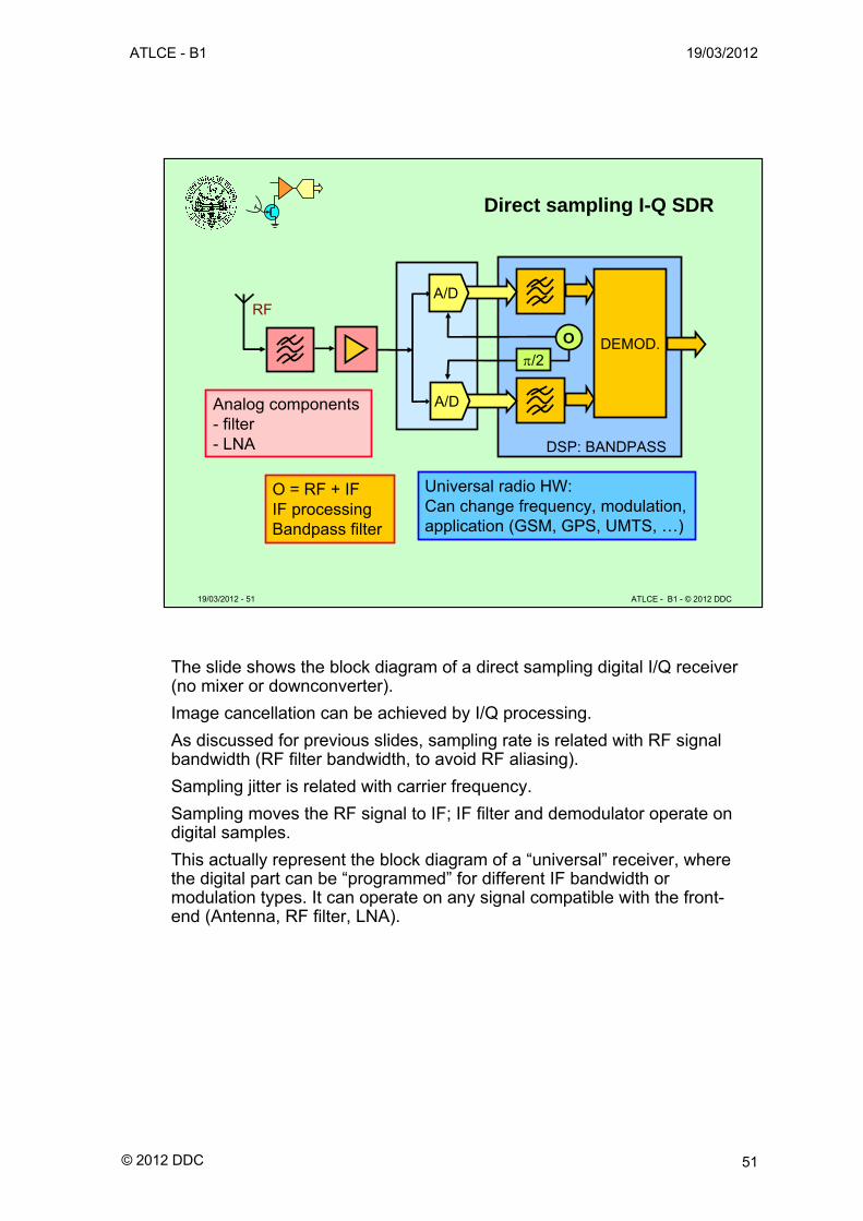
Direct sampling I-Q SDR
DSP: BANDPASS
Analog components- filter- LNA
RF
DEMOD.
A/D
A/D
O
/2
Universal radio HW:Can change frequency, modulation, application (GSM, GPS, UMTS, …)
O = RF + IFIF processingBandpass filter
The slide shows the block diagram of a direct sampling digital I/Q receiver (no mixer or downconverter).
Image cancellation can be achieved by I/Q processing.
As discussed for previous slides, sampling rate is related with RF signal bandwidth (RF filter bandwidth, to avoid RF aliasing).
Sampling jitter is related with carrier frequency.
Sampling moves the RF signal to IF; IF filter and demodulator operate on digital samples.
This actually represent the block diagram of a “universal” receiver, where the digital part can be “programmed” for different IF bandwidth or modulation types. It can operate on any signal compatible with the front-end (Antenna, RF filter, LNA).
ATLCE - B1 19/03/2012
© 2012 DDC 52
19/03/2012 - 52 ATLCE - B1 - © 2012 DDC
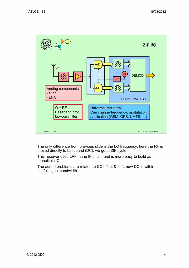
ZIF I/Q
DSP: LOWPASS
Va
DEMOD.
A/D
A/D
O
/2
Analog components- filter- LNA
Universal radio HW:Can change frequency, modulation, application (GSM, GPS, UMTS, …)
O = RFBaseband proc.Lowpass filter
The only difference from previous slide is the LO frequency: here the RF is moved directly to baseband (DC); we get a ZIF system
This receiver used LPF in the IF chain, and is more easy to build as monolithic IC.
The added problems are related to DC offset & drift; now DC in within useful signal bandwidth.

ATLCE - B1 19/03/2012
© 2012 DDC 53
19/03/2012 - 53 ATLCE - B1 - © 2012 DDC
Lesson B1: radio system architectures
• Heterodyne receivers
• The image problem
• Dual conversion receivers
• Complex mixer & I/Q processing
• Digital receivers
• Software Defined Radio
• Examples
ATLCE - B1 19/03/2012
© 2012 DDC 54
19/03/2012 - 54 ATLCE - B1 - © 2012 DDC
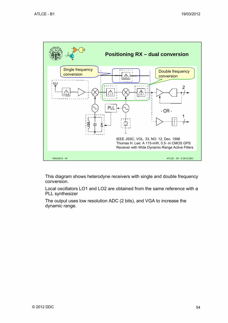
Positioning RX – dual conversion
IEEE JSSC, VOL. 33, NO. 12, Dec. 1998Thomas H. Lee: A 115-mW, 0.5- m CMOS GPS Receiver with Wide Dynamic-Range Active Filters
Single frequencyconversion
Double frequencyconversion
This diagram shows heterodyne receivers with single and double frequency conversion.
Local oscillators LO1 and LO2 are obtained from the same reference with a PLL synthesizer
The output uses low resolution ADC (2 bits), and VGA to increase the dynamic range.
ATLCE - B1 19/03/2012
© 2012 DDC 55
19/03/2012 - 55 ATLCE - B1 - © 2012 DDC
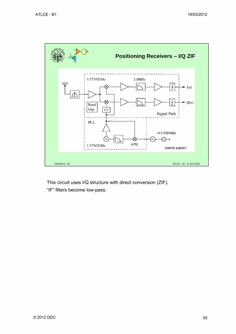
Positioning Receivers – I/Q ZIF
(same paper)
This circuit uses I/Q structure with direct conversion (ZIF).
“IF” filters become low-pass.
ATLCE - B1 19/03/2012
© 2012 DDC 56
19/03/2012 - 56 ATLCE - B1 - © 2012 DDC
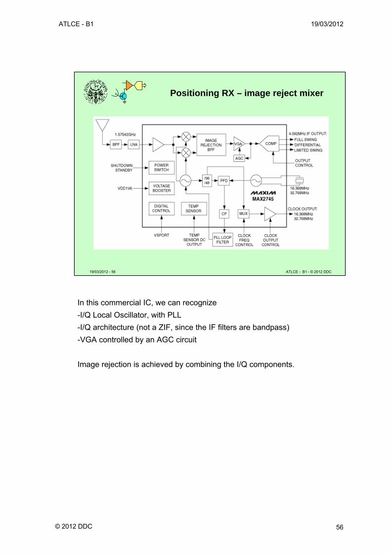
Positioning RX – image reject mixer
In this commercial IC, we can recognize
-I/Q Local Oscillator, with PLL
-I/Q architecture (not a ZIF, since the IF filters are bandpass)
-VGA controlled by an AGC circuit
Image rejection is achieved by combining the I/Q components.
ATLCE - B1 19/03/2012
© 2012 DDC 57
19/03/2012 - 57 ATLCE - B1 - © 2012 DDC
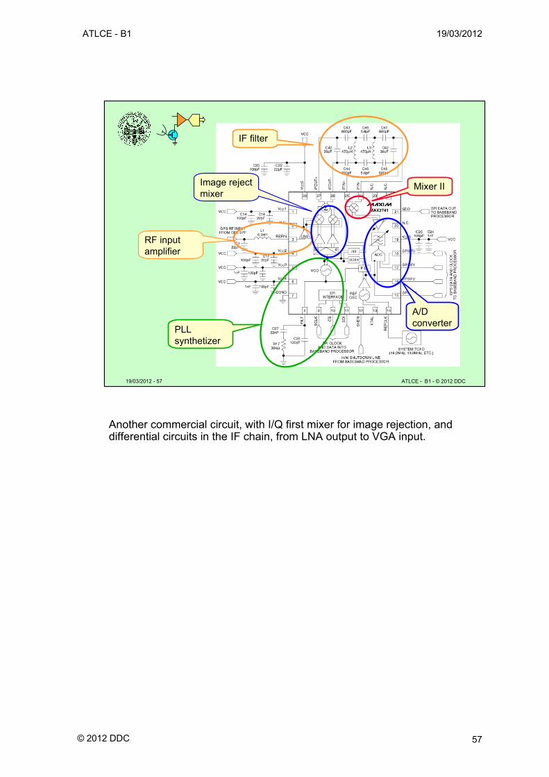
Complete RX
Image rejectmixer
RF input amplifier
PLL synthetizer
Mixer II
IF filter
A/D converter
Another commercial circuit, with I/Q first mixer for image rejection, and differential circuits in the IF chain, from LNA output to VGA input.
ATLCE - B1 19/03/2012
© 2012 DDC 58
19/03/2012 - 58 ATLCE - B1 - © 2012 DDC
The transmitter chain
• Conventional– Generate carrier
– Modulate
– Filter and Amplify (PA)
• Reverse heterodyne receiver chain– Generate baseband modulated signal
– Filter and translate to RF
– Filter and amplify (PA)
• Next – Direct generation of RF (high speed DAC)
– Digital correction of PA nonlinearity
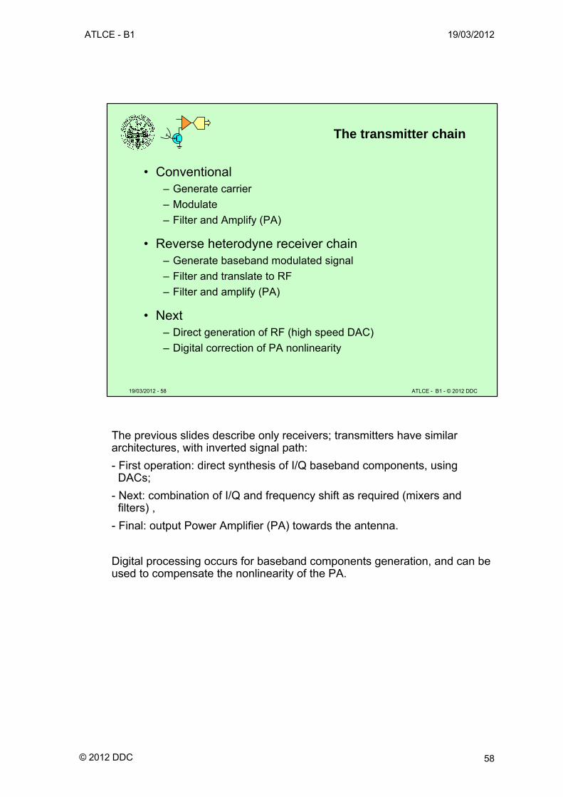
The previous slides describe only receivers; transmitters have similar architectures, with inverted signal path:
- First operation: direct synthesis of I/Q baseband components, usingDACs;
- Next: combination of I/Q and frequency shift as required (mixers andfilters) ,
- Final: output Power Amplifier (PA) towards the antenna.
Digital processing occurs for baseband components generation, and can be used to compensate the nonlinearity of the PA.
ATLCE - B1 19/03/2012
© 2012 DDC 59
19/03/2012 - 59 ATLCE - B1 - © 2012 DDC
Complete RTX structure
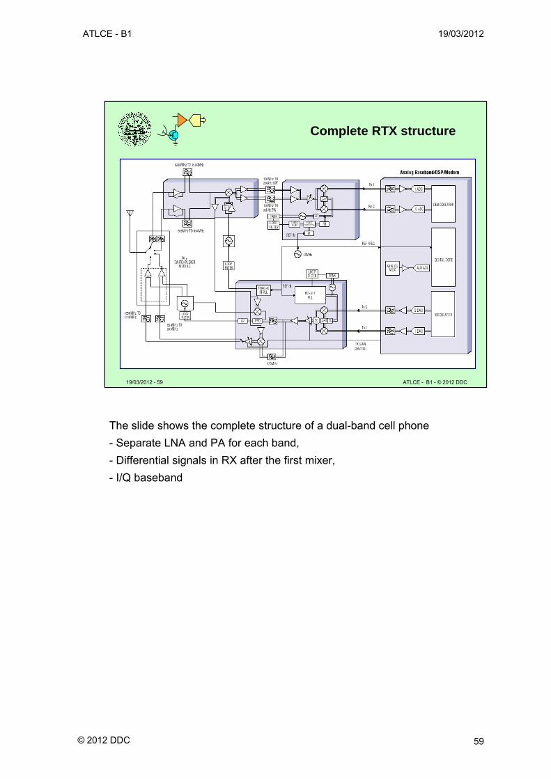
The slide shows the complete structure of a dual-band cell phone
- Separate LNA and PA for each band,
- Differential signals in RX after the first mixer,
- I/Q baseband
ATLCE - B1 19/03/2012
© 2012 DDC 60
19/03/2012 - 60 ATLCE - B1 - © 2012 DDC
Details of receiver I/Q chain
Section of the receiver chain:- filters, amplifiers, PLL, mixer- A/D converters- Numeric demodulator
Signal flow
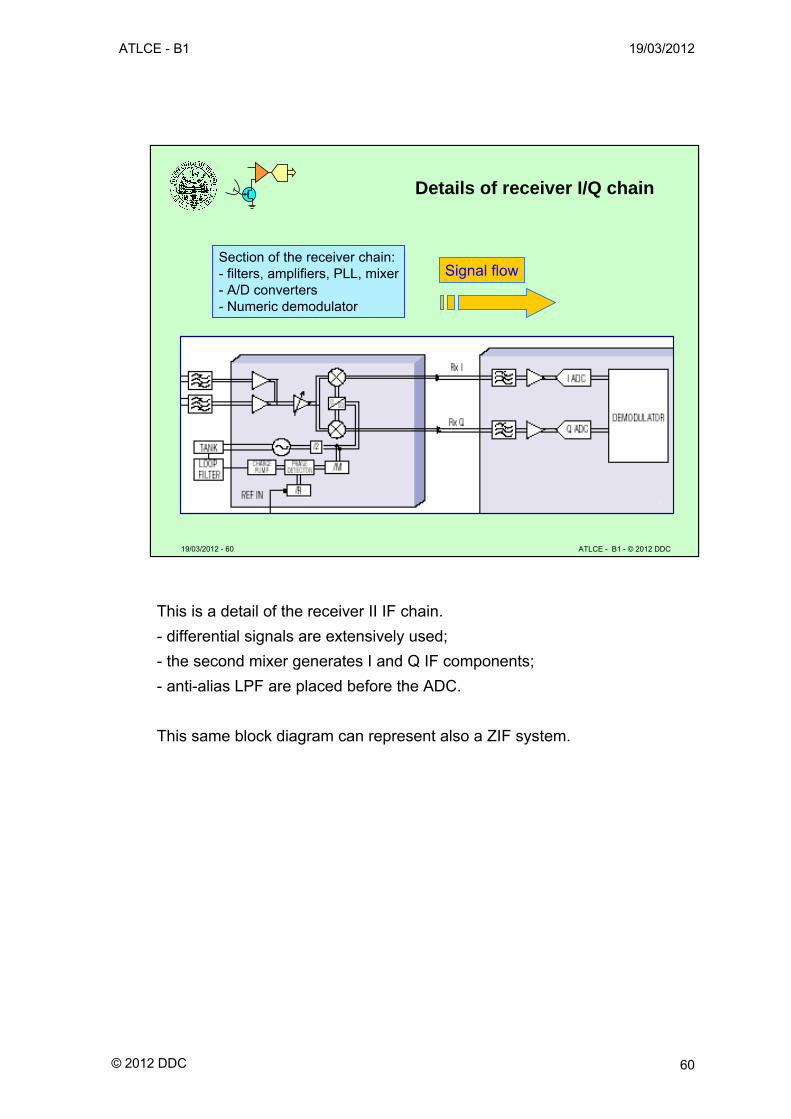
This is a detail of the receiver II IF chain.
- differential signals are extensively used;
- the second mixer generates I and Q IF components;
- anti-alias LPF are placed before the ADC.
This same block diagram can represent also a ZIF system.
ATLCE - B1 19/03/2012
© 2012 DDC 61
19/03/2012 - 61 ATLCE - B1 - © 2012 DDC
I/Q transmitter structure
Section of the transmission chain:- D/A converters, - amplifiers, filters- PLL, mixer,
Signal flow
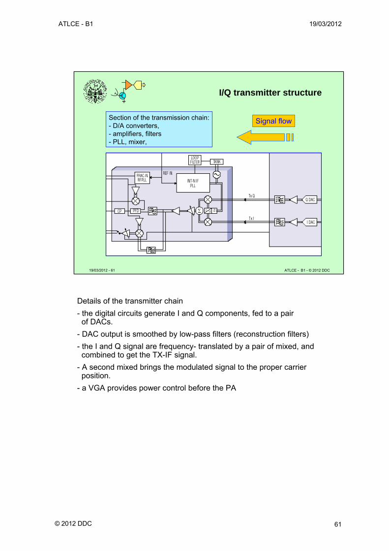
Details of the transmitter chain
- the digital circuits generate I and Q components, fed to a pairof DACs.
- DAC output is smoothed by low-pass filters (reconstruction filters)
- the I and Q signal are frequency- translated by a pair of mixed, andcombined to get the TX-IF signal.
- A second mixed brings the modulated signal to the proper carrierposition.
- a VGA provides power control before the PA
ATLCE - B1 19/03/2012
© 2012 DDC 62
19/03/2012 - 62 ATLCE - B1 - © 2012 DDC
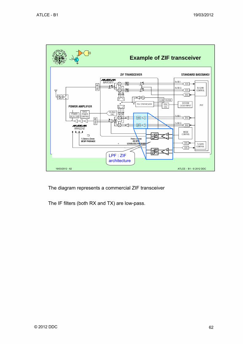
Example of ZIF transceiver
LPF : ZIF architecture
The diagram represents a commercial ZIF transceiver
The IF filters (both RX and TX) are low-pass.
ATLCE - B1 19/03/2012
© 2012 DDC 63
19/03/2012 - 63 ATLCE - B1 - © 2012 DDC
PLLDDS
X
ANTENNA
DEM.
XX
X
D/A
CONTROL
A/D
D/A
Mike, Earph., Display, Keys
D/A
O O I/Q I/Q
X
A/D
A/D
XMOD.
RF: 0,9/2GHz
MIXED A/DIF: 100 MHz
BASEBAND DIGITAL
TRANSDUCERS
Low Noise Amplifier900MHz/2GHz
Power Amplifier900MHz/2GHz
IF RX channel
IF TX channel
I/Q RX channel
Oscillators and synthesizers
I/Q TX channel
µP, DSP, memory, ..
User Interface
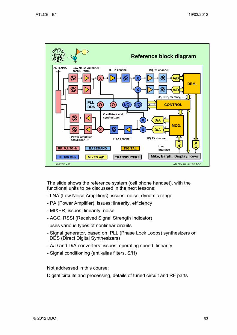
Reference block diagram
The slide shows the reference system (cell phone handset), with the functional units to be discussed in the next lessons:
- LNA (Low Noise Amplifiers); issues: noise, dynamic range
- PA (Power Amplifier); issues: linearity, efficiency
- MIXER; issues: linearity, noise
- AGC, RSSI (Received Signal Strength Indicator)
uses various types of nonlinear circuits
- Signal generator, based on PLL (Phase Lock Loops) synthesizers orDDS (Direct Digital Synthesizers)
- A/D and D/A converters; issues: operating speed, linearity
- Signal conditioning (anti-alias filters, S/H)
Not addressed in this course:
Digital circuits and processing, details of tuned circuit and RF parts
ATLCE - B1 19/03/2012
© 2012 DDC 64
19/03/2012 - 64 ATLCE - B1 - © 2012 DDC
:
Lesson B1 – final test
• Which are the benefits of heterodyne receivers?
• Explain the image frequency problem.
• Which filter is used for channel separation?
• Why do some receivers use dual conversion?
• Which techniques are used for image rejection?
• What do AGC and VGA mean?
• Describe the architecture of a SW radio.
• Draw the block diagram of a receiver with digital I/Q processingfor image cancelation.
• Which is the minimum sampling rate (Fs) for a signal with 2.5 GHz carrier, and a bandwidth of 2 MHz?
-:
-