Embed Size (px)
Citation preview
IDEC 혼성 모드 시스템 설계 및 실습
CMOS analog filter design
Changsik YooDepartment of Electronics and Computer Engineering
Hanyang University, Seoul, [email protected]

Winter Course of IT SoC Center (Dec. 13-17, 2004)
Introduction
3
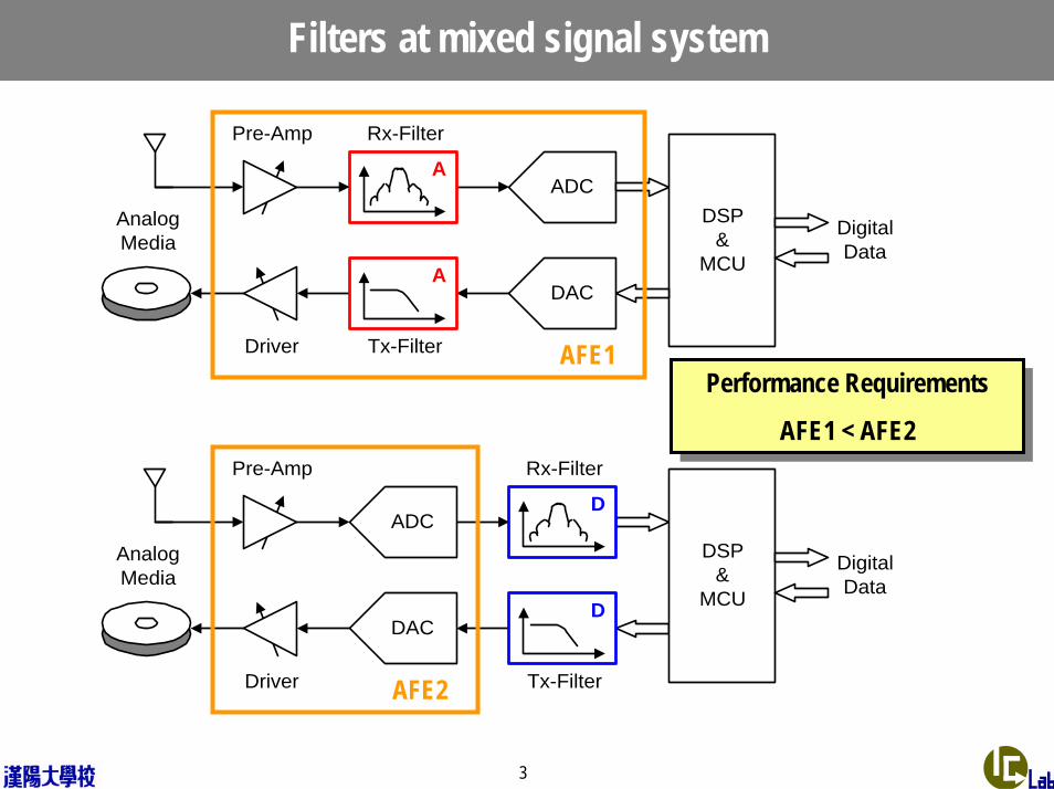
Filters at mixed signal system
AnalogMedia
Pre-Amp Rx-Filter
ADC
DAC
Tx-FilterDriver
DSP&
MCU
DigitalData
A
A
AnalogMedia
Pre-Amp Rx-Filter
ADC
DAC
Tx-FilterDriver
DSP&
MCU
DigitalData
D
D
AFE1
AFE2
Performance Requirements
AFE1 < AFE2
Performance Requirements
AFE1 < AFE2
4
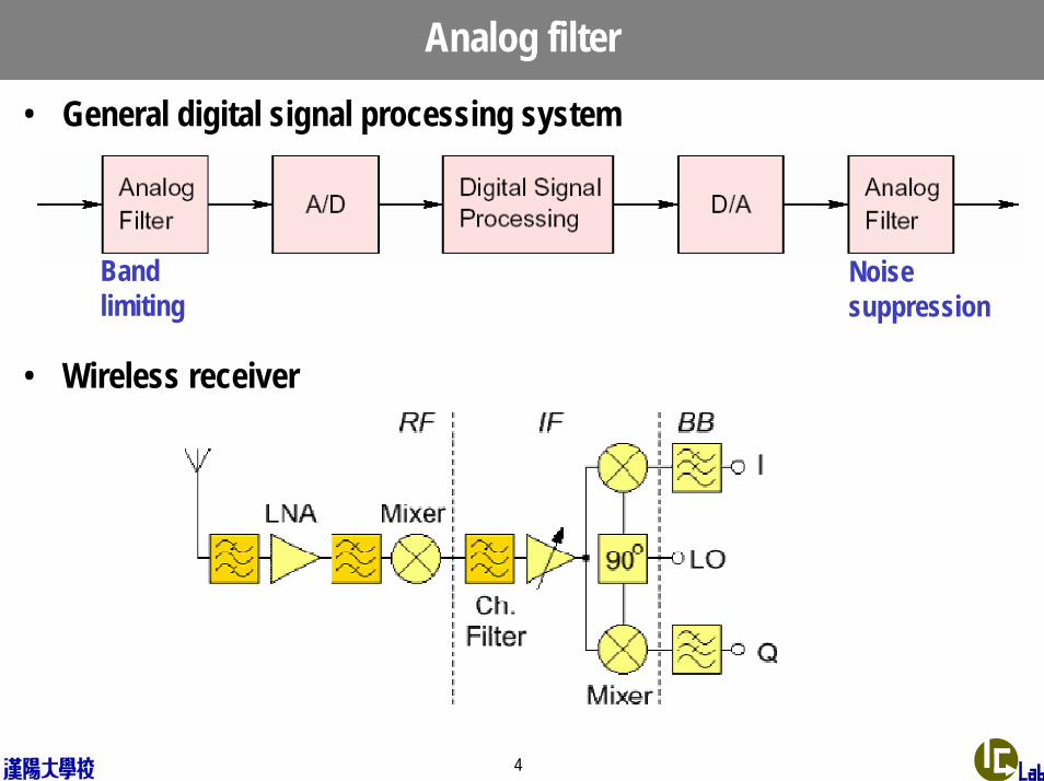
Analog filter
• General digital signal processing system
Band limiting
Noise suppression
• Wireless receiver
5
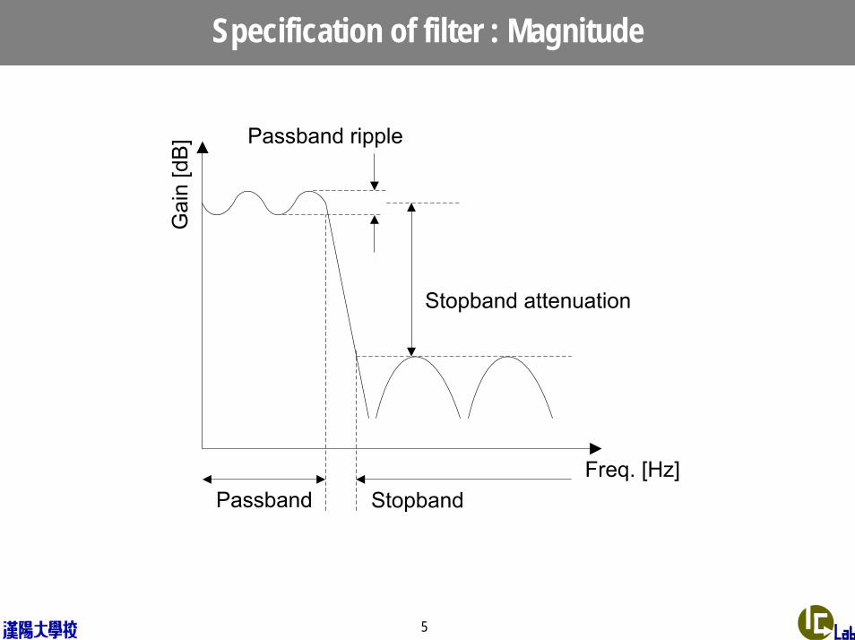
Specification of filter : Magnitude
6
Specification of filter : Phase
• Phase response is also important.– Equal phase for all frequencies is not desired.– Equal delay (group delay) for all frequencies is desired.
• For equal group delay, phase response should be linear function of frequency.
• For certain type of filters, the variation of group delay may be too large to be tolerated for target application.– Group delay equalization is required for some applications such as data
communication system.– All pass filter with group delay equalization

7
Types of filter
Butterworth : Maximally flat gain
Chebyshev :Equiripple in passband
Inverse Chebyshev :Equiripple in stopband
Elliptic (Cauer) :Equiripple in pass/stopband
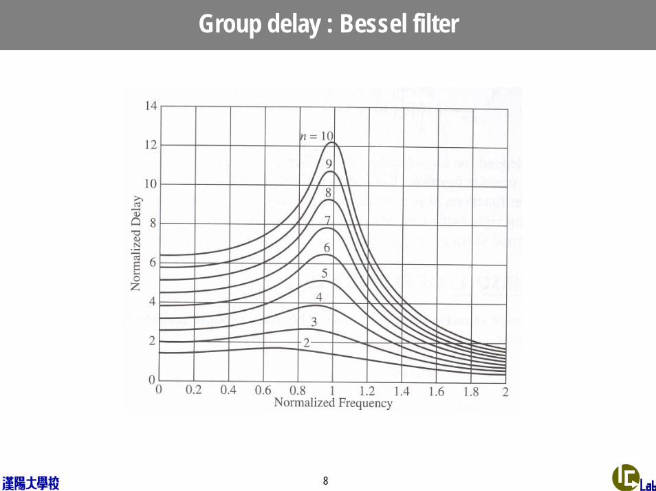
Bessel :Maximally flat group delay
8
Group delay : Bessel filter
9
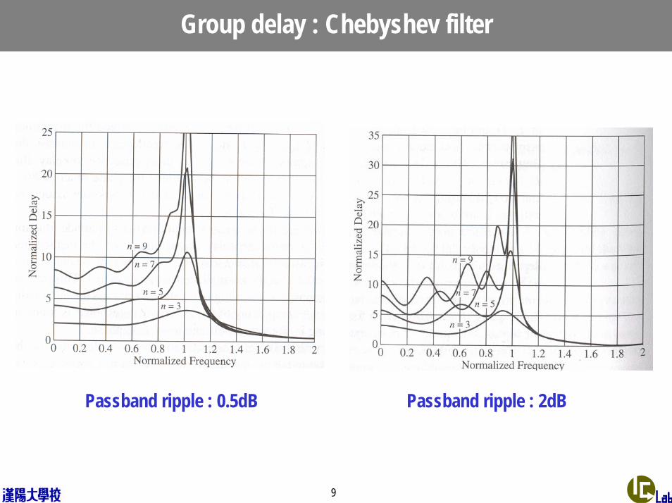
Group delay : Chebyshev filter
Passband ripple : 0.5dB Passband ripple : 2dB
10
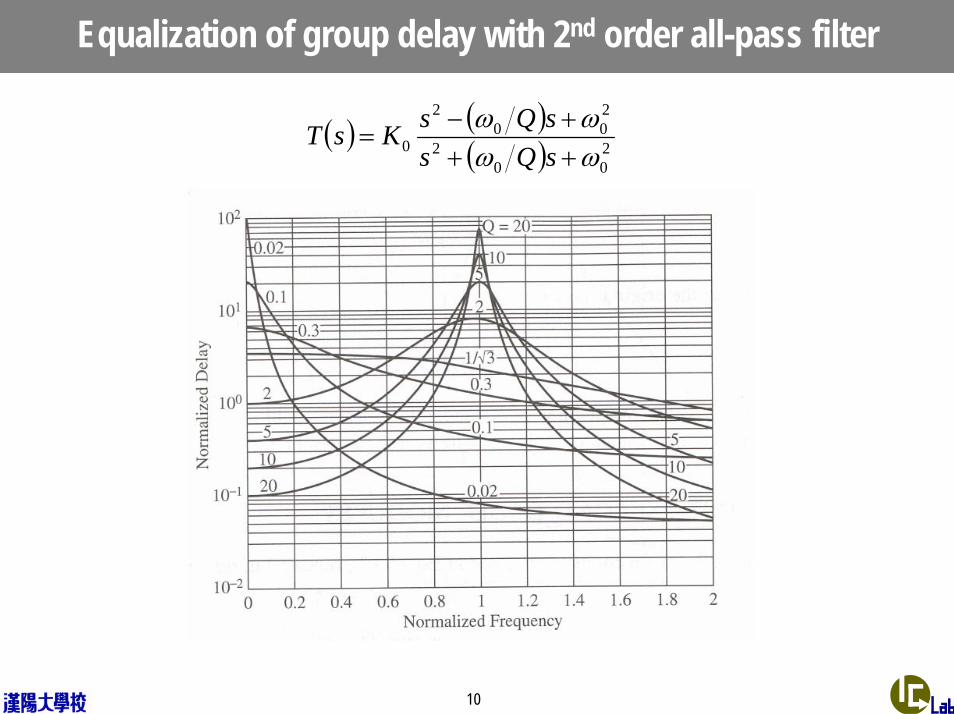
Equalization of group delay with 2nd order all-pass filter
( ) ( )( ) 2
002
200
2
0 ωωωω
+++−
=sQssQsKsT
11
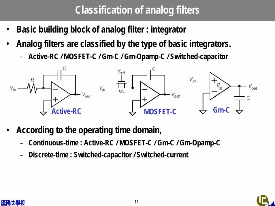
Classification of analog filters• Basic building block of analog filter : integrator• Analog filters are classified by the type of basic integrators.
– Active-RC / MOSFET-C / Gm-C / Gm-Opamp-C / Switched-capacitor
• According to the operating time domain, – Continuous-time : Active-RC / MOSFET-C / Gm-C / Gm-Opamp-C – Discrete-time : Switched-capacitor / Switched-current
Active-RC MOSFET-C Gm-C

12
Continuous-time filter• Gm-C, active-RC, MOSFET-C filter…• No pre- and post- processing required• Tuning circuits required to have desired frequency characteristics
1NN1N
2N
1
1MM1M
2M
1
asasasabsbsbsb
)s(Y)s(X)s(H
+−
+−
++++++++
=≡
-0.5 0 0.5-5
-4
-3
-2
-1
0
1
2
3
4
5
real f [MHz]
imag
inar
y f [
MH
z]
100 102 104 106 108-120
-100
-80
-60
-40
-20
0
f [Hz]
|H(f)
| [dB
]
13
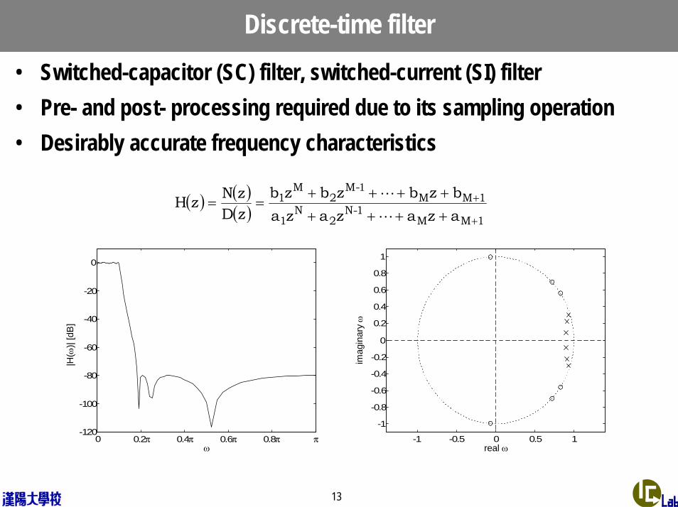
Discrete-time filter• Switched-capacitor (SC) filter, switched-current (SI) filter• Pre- and post- processing required due to its sampling operation• Desirably accurate frequency characteristics
0 0.2π 0.4π 0.6π 0.8π π-120
-100
-80
-60
-40
-20
0
ω
|H(ω
)| [d
B]
-1 -0.5 0 0.5 1
-1
-0.8
-0.6
-0.4
-0.2
0
0.2
0.4
0.6
0.8
1
real ω
imag
inar
y ω
( ) ( )( ) 1MM
1N-2
N1
1MMM-
2M
1
azazazabzbzbzb
zDzNzH
+
+
++++
++++==
1
14
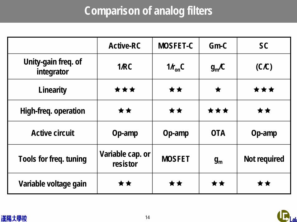
Comparison of analog filters
Active-RC MOSFET-C Gm-C SC
Unity-gain freq. of integrator 1/RC 1/ronC gm/C (C/C)
Linearity
High-freq. operation
Active circuit Op-amp Op-amp OTA Op-amp
Tools for freq. tuning Variable cap. or resistor MOSFET gm Not required
Variable voltage gain
15
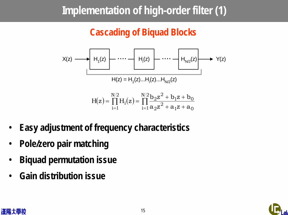
Implementation of high-order filter (1)
Cascading of Biquad Blocks
Hi(z) HN/2(z)H1(z) .... ....X(z) Y(z)
H(z) = H1(z)...Hi(z)...HN/2(z)
( ) ( ) ∏∏== ++
++==
2N
1i 012
2
012
22N
1ii azaza
bzbzbzHzH
• Easy adjustment of frequency characteristics• Pole/zero pair matching• Biquad permutation issue• Gain distribution issue
16
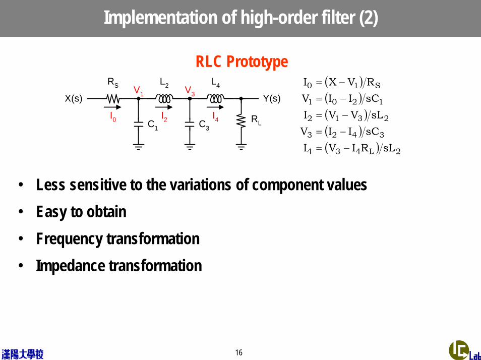
Implementation of high-order filter (2)
RLC Prototype
C1
RS
X(s) Y(s)
RLC3
L2 L4
I2 I4
V1 V3
I0
( )( )( )( )( ) 2L434
3423
2312
1201
S10
sLRIVIsCIIVsLVVI
sCIIVRVXI
−=
−=
−=
−=−=
• Less sensitive to the variations of component values• Easy to obtain• Frequency transformation• Impedance transformation
17
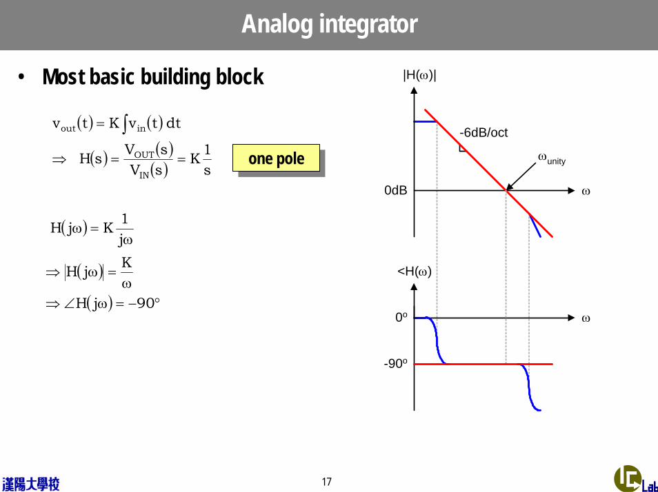
Analog integrator
• Most basic building block |H(ω)|
ω0dB
ωunity
-6dB/oct
<H(ω)
ω0o
-90o
( ) ( )
( ) ( )( ) s
1KsVsVsH
dttvKtv
IN
OUT
inout
==⇒
= ∫
one poleone pole
( )
( )
( ) 90jH
KjH
j1KjH
°−=ω∠⇒ω
=ω⇒
ω=ω
18
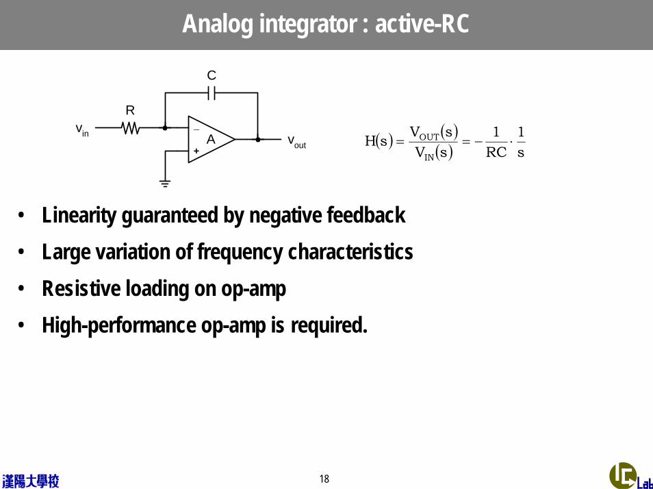
Analog integrator : active-RC
Rvin vout
C
+
_A ( ) ( )
( ) s1
RC1
sVsVsH
IN
OUT ⋅−==
• Linearity guaranteed by negative feedback• Large variation of frequency characteristics • Resistive loading on op-amp• High-performance op-amp is required.

19
Analog integrator : MOSFET-C
RON
vin vout
C
+
_A ( ) ( )
( ) s1
CR1
sVsVsH
ONIN
OUT ⋅−==
• Linearity guaranteed by negative feedback but somewhat degraded due to the non-linear resistance of MOSFET
• Large variation of frequency characteristics• Resistive loading on op-amp• High-performance op-amp is required.
20
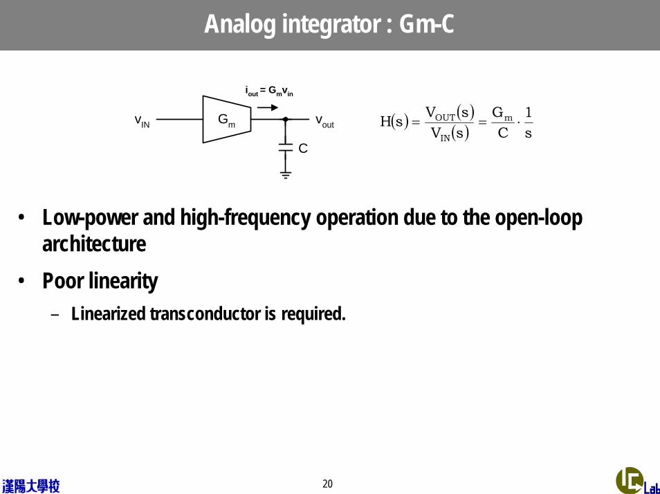
Analog integrator : Gm-C
vIN voutGm
iout = Gmvin
C
( ) ( )( ) s
1C
GsVsVsH m
IN
OUT ⋅==
• Low-power and high-frequency operation due to the open-loop architecture
• Poor linearity– Linearized transconductor is required.

21
Analog integrator : SC
+-
C2C1 φ2φ1vin vout
φ1φ2
( ) ( )( ) 1
1
2
1
IN
OUT
z1z
CC
zVzVzH −
−
−⋅==
• Accurate frequency characteristics• Linearity guaranteed by negative feedback• Large power dissipation for high frequency operation (fclk >> fsignal)• Anti-aliasing and smoothing filter required
IDEC 혼성 모드 시스템 설계 및 실습
Active-RC / MOSFET-C filter
23
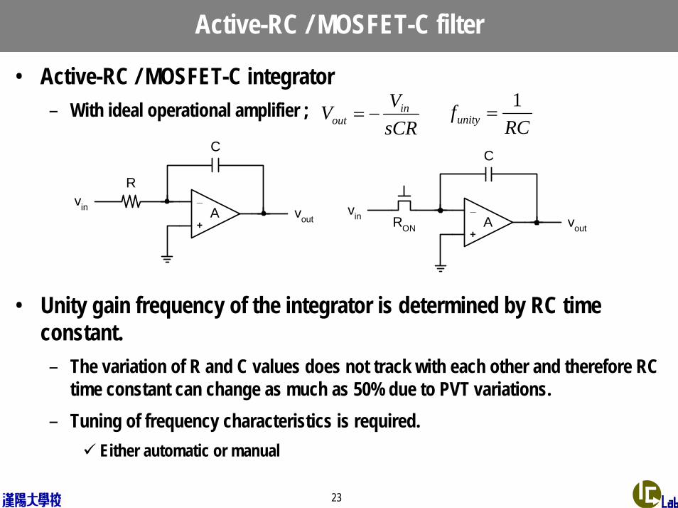
Active-RC / MOSFET-C filter
• Active-RC / MOSFET-C integrator– With ideal operational amplifier ;
• Unity gain frequency of the integrator is determined by RC time constant.– The variation of R and C values does not track with each other and therefore RC
time constant can change as much as 50% due to PVT variations.– Tuning of frequency characteristics is required.
Either automatic or manual
sCRVV in
out −=RC
funity1
=
Rvin vout
C
+
_A
RON
vin vout
C
+
_A
24
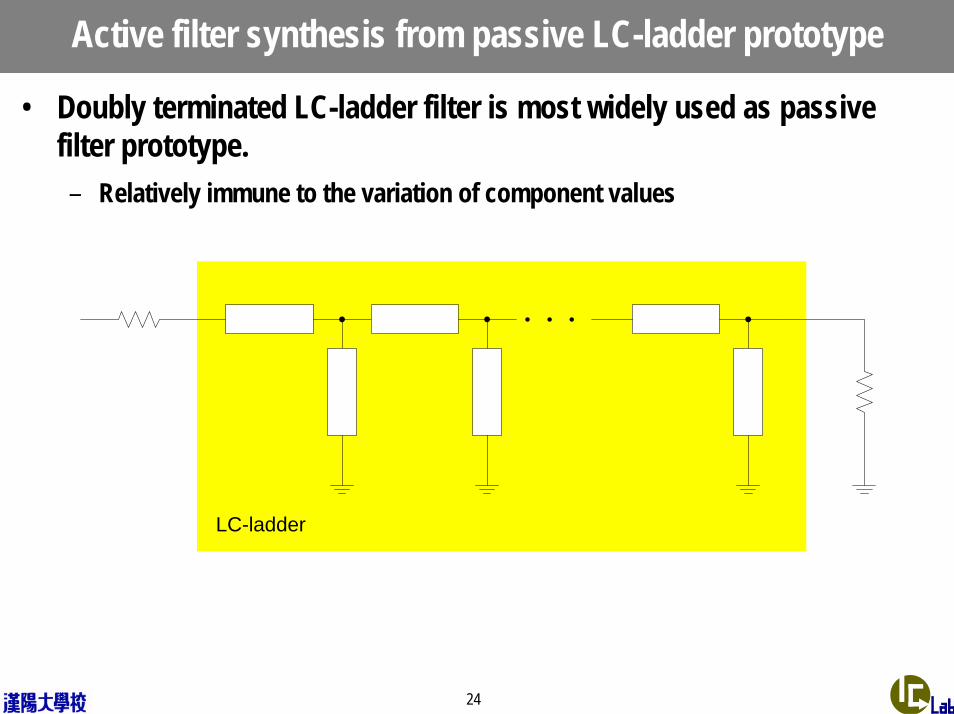
Active filter synthesis from passive LC-ladder prototype
• Doubly terminated LC-ladder filter is most widely used as passive filter prototype.– Relatively immune to the variation of component values
LC-ladder
25
Synthesis of active filter from passive prototype
• Element substitution– R : R in active-RC filter– C : C– L : Gyrator
• Signal flow graph (SFG)– Same result as with element substitution– Useful for optimization (e.g. dynamic range optimization)– Will be explained in next slides.
26
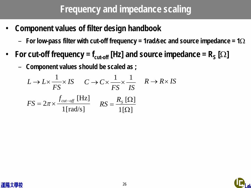
Frequency and impedance scaling
• Component values of filter design handbook – For low-pass filter with cut-off frequency = 1rad/sec and source impedance = 1Ω
• For cut-off frequency = fcut-off [Hz] and source impedance = RS [Ω]– Component values should be scaled as ;
ISFS
LL ××→1
ISFSCC 11
××→ ISRR ×→
]rad/s[ 1[Hz]
2 offcutfFS −×= π
][ 1][
ΩΩ
= SRRS
27
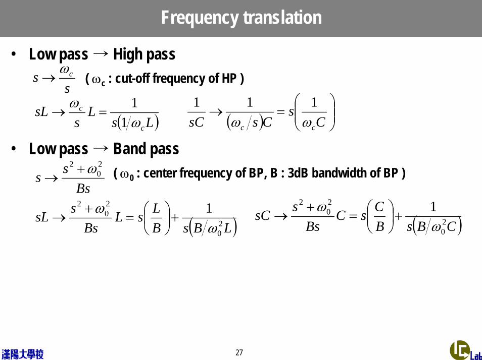
Frequency translation
• Low pass → High pass( ωc : cut-off frequency of HP )
• Low pass → Band pass( ω0 : center frequency of BP, B : 3dB bandwidth of BP )
ss cω→
( )LsL
ssL
c
c
ωω
11
=→ ( ) ⎟⎟⎠
⎞⎜⎜⎝
⎛=→
Cs
CssC cc ωω111
Bsss
20
2 ω+→
( )LBsBLsL
BsssL 2
0
20
2 1ω
ω+⎟
⎠⎞
⎜⎝⎛=
+→ ( )CBsB
CsCBs
ssC 20
20
2 1ω
ω+⎟
⎠⎞
⎜⎝⎛=
+→
28
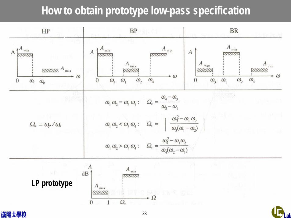
How to obtain prototype low-pass specification
LP prototype
29
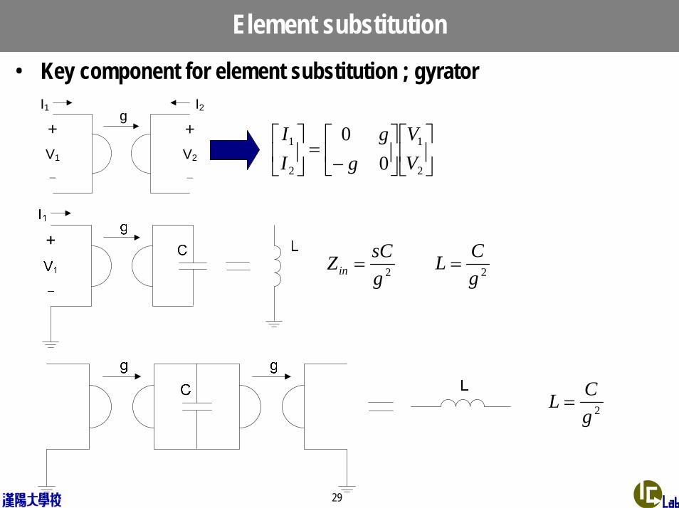
Element substitution• Key component for element substitution ; gyrator
gI1 I2
V1 V2
+
_
+
_⎥⎦
⎤⎢⎣
⎡⎥⎦
⎤⎢⎣
⎡−
=⎥⎦
⎤⎢⎣
⎡
2
1
2
1
00
VV
gg
II
2gsCZin = 2g
CL =
2gCL =
30
Signal flow graph (SFG)
• Graphical representation of KCL and KVL• Good design tool for analog filter synthesis• Some tips for analog filter synthesis
– Transfer function does not change as long as the loop gain is conserved.This property will be utilized for dynamic range optimization.
– Vertex variables (see the example on the next slide)Source voltageVoltage across shunt branchesCurrent through series branches
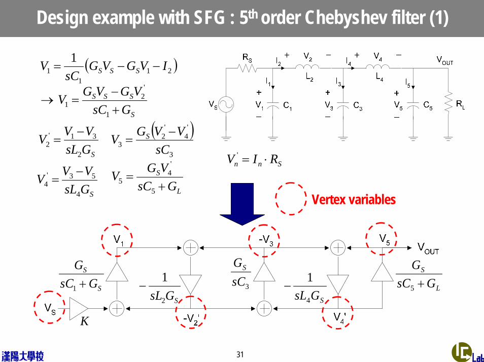
31
Design example with SFG : 5th order Chebyshev filter (1)
( )
S
SSS
SSS
GsCVGVGV
IVGVGsC
V
+−
=→
−−=
1
'2
1
211
1
1
SGsLVVV
2
31'2
−=
( )3
'4
'2
3 sCVVGV S −
=
SGsLVVV
4
53'4
−=
L
S
GsCVGV+
=5
'4
5
Snn RIV ⋅='
S
S
GsCG+1
K
SGsL2
1− 3sC
GS
SGsL4
1− L
S
GsCG+5
Vertex variables
32
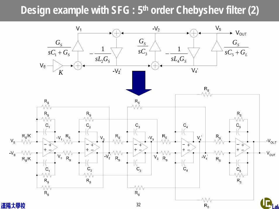
Design example with SFG : 5th order Chebyshev filter (2)
S
S
GsCG+1
K
SGsL2
1− 3sC
GS
SGsL4
1− L
S
GsCG+5
33
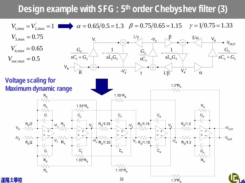
Design example with SFG : 5th order Chebyshev filter (3)1'
max,2max,1 ==VV75.0max,3 =V
65.0'max,4 =V
5.0max, =outV S
S
GsCG+1
K
SGsL2
1−
3sCGS
SGsL4
1−
L
S
GsCG+5
3.15.065.0 ==α 15.165.075.0 ==β 33.175.01 ==γ
Voltage scaling forMaximum dynamic range
34
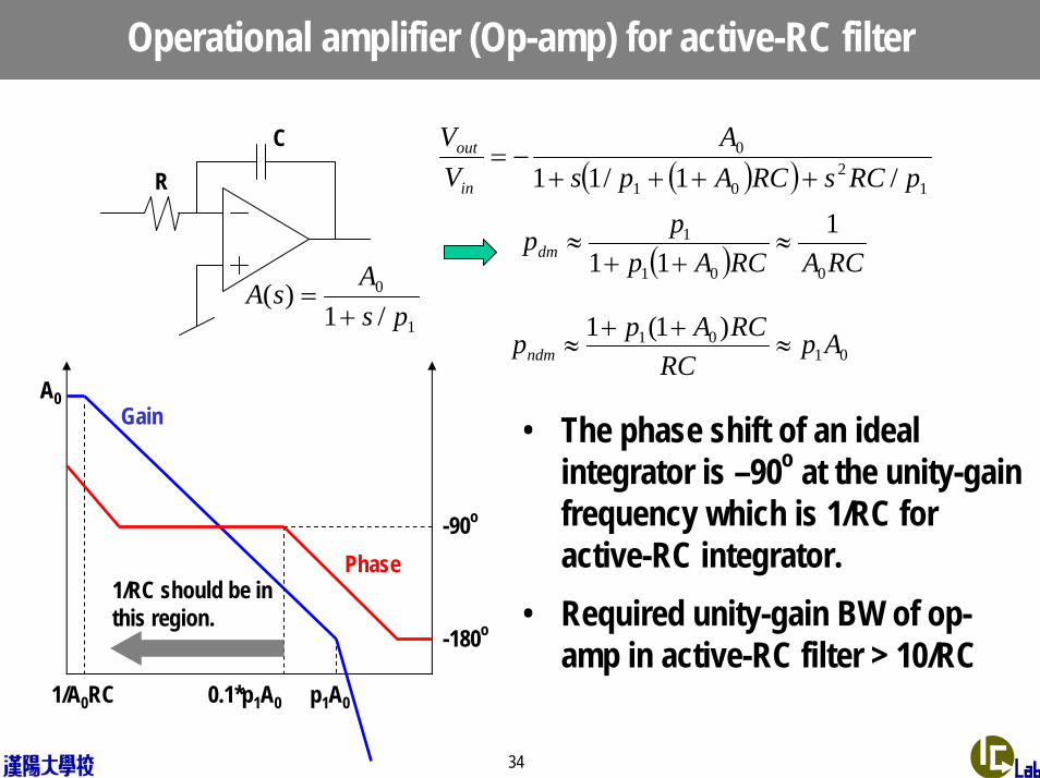
Operational amplifier (Op-amp) for active-RC filter
R
C
1
0
/1)(
psA
sA+
=
( )( ) 12
01
0
/1/11 pRCsRCApsA
VV
in
out
++++−=
( ) RCARCApppdm
001
1 111
≈++
≈
0101 )1(1 Ap
RCRCAppndm ≈
++≈
1/A0RC p1A0
A0
-90o
-180o
Gain
Phase
0.1*p1A0
1/RC should be in this region.
• The phase shift of an ideal integrator is –90o at the unity-gain frequency which is 1/RC for active-RC integrator.
• Required unity-gain BW of op-amp in active-RC filter > 10/RC
IDEC 혼성 모드 시스템 설계 및 실습
Gm-C filter
36
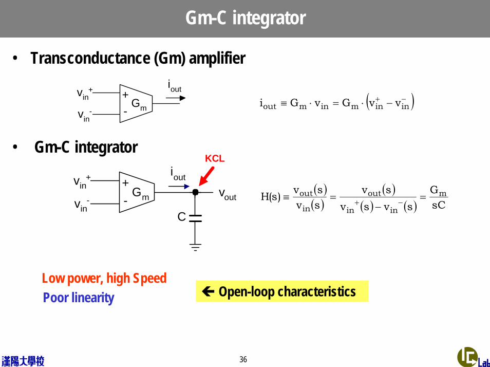
Gm-C integrator
• Transconductance (Gm) amplifier
• Gm-C integrator
Low power, high SpeedPoor linearity
Gm+-
ioutvin+
vin-
( ) vvGvGi ininminmout−+ −⋅=⋅≡
Gm+-
ioutvin+
vin-
vout
C
KCL
( )( )
( )( ) ( ) sC
Gsvsv
svsvsv)s(H m
inin
out
in
out =−
=≡ −+
Open-loop characteristics

37
Gm amplifier basics
• Transconductance (Gm) amplifier
Single-ended Fully-differential
• Transconductance amplifier characteristics– Linearity– I/O impedances– Operating (dynamic) range– Frequency characteristics– Electrically programmable Gm value
Gm+-
ioutvin+
vin-
Gm
+-
ioutvin+
vin-
iout
+-
( ) vvGvGi ininminmout−+ −⋅=⋅≡
R , R outin ∞=∞=
38
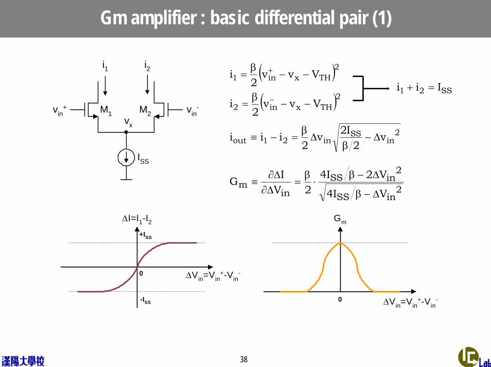
Gm amplifier : basic differential pair (1)
( )( )2THxin2
2THxin1
Vvv2
i
Vvv2
i
−−β
=
−−β
=
−
+
M1 M2vin+ vin
-
i2i1
ISS
vx
SS21 Iii =+
2in
SSin21out v
2I2v
2iii ∆−
β∆
β=−≡
2inSS
2inSS
inm
VI4
V2I42V
IG∆−β
∆−β⋅
β=
∆∂∆∂
≡
0 ∆Vin=Vin+-Vin
-
+ISS
∆I=I1-I2
-ISS 0
Gm
∆Vin=Vin+-Vin
-
39
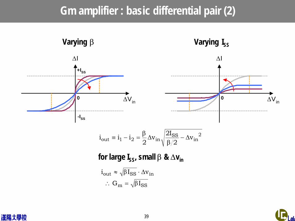
Gm amplifier : basic differential pair (2)
Varying β Varying ISS
0 ∆Vin
+ISS
∆I
-ISS
0 ∆Vin
∆I
2in
SSin21out v
2I2v
2iii ∆−
β∆
β=−≡
for large ISS, small β & ∆vin
SSm
inSSout
IG
vIi
β=∴
∆⋅β≈
40
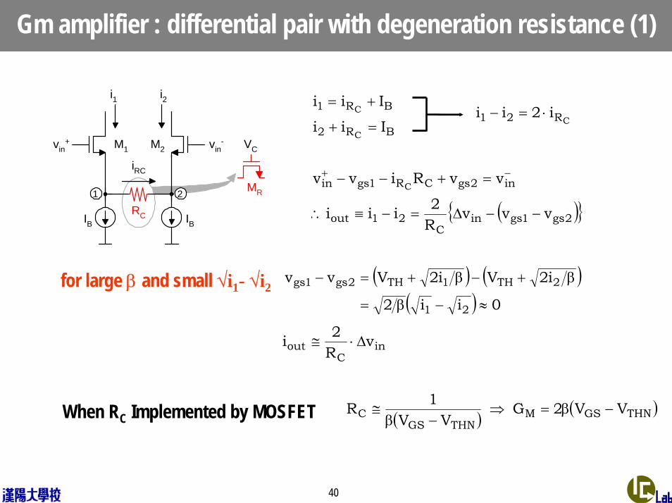
Gm amplifier : differential pair with degeneration resistance (1)
M1 M2vin+ vin
-
i2i1
IBRC IB
MR
VC
iRC
1 2
BR2
BR1
Iii
Iii
C
C
=+
+=CR21 i2ii ⋅=−
( ) 2gs1gsinC
21out
in2gsCR1gsin
vvvR2iii
vvRivvC
−−∆=−≡∴
=+−− −+
( ) ( )( ) 0ii2
i2Vi2Vvv
21
2TH1TH2gs1gs
≈−β=
β+−β+=−for large β and small √i1- √i2
inC
out vR2i ∆⋅≅
( ) ( )THNGSMTHNGS
C VV2G VV
1R −β=⇒−β
≅When RC Implemented by MOSFET
41
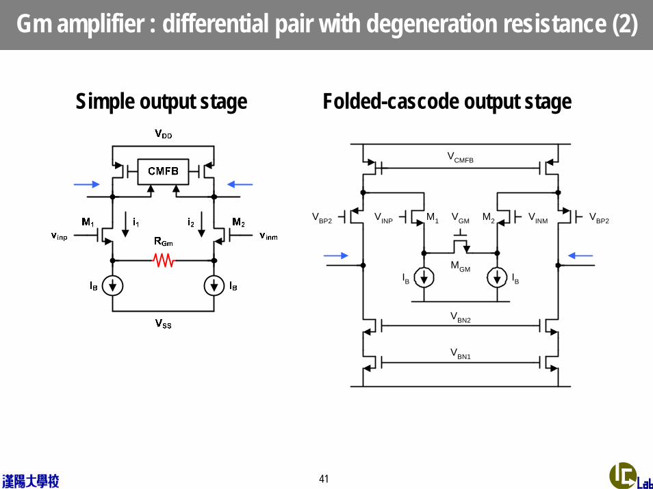
Gm amplifier : differential pair with degeneration resistance (2)
Simple output stage Folded-cascode output stage
M1 M2
MGM
VINMVINP
IB IB
VCMFB
VBP2VBP2
VBN1
VBN2
VGM
42
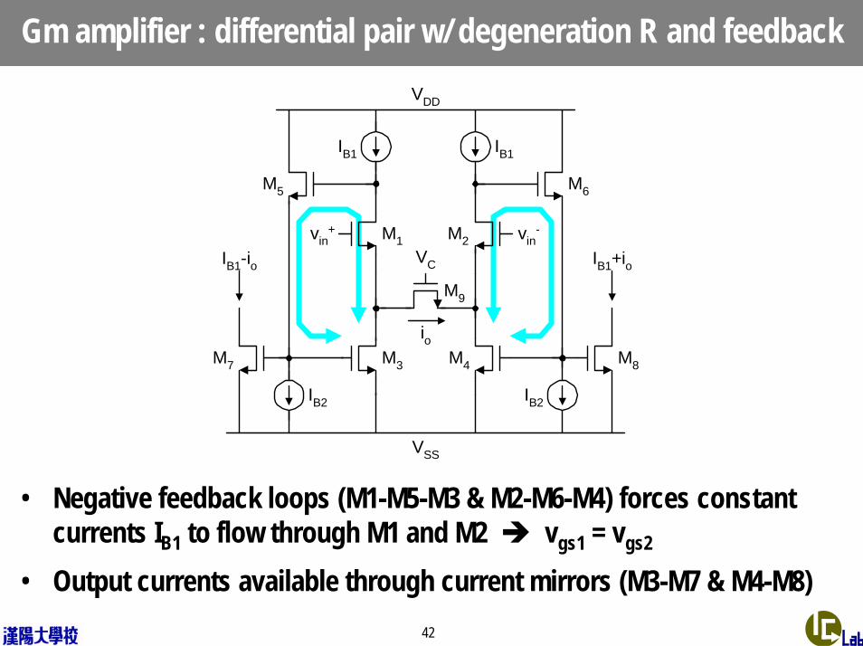
Gm amplifier : differential pair w/ degeneration R and feedback
M1 M2vin+ vin
-
VC
M9
M3 M4
M5 M6
M7 M8
IB1 IB1
IB2 IB2
IB1-io IB1+io
io
VDD
VSS
• Negative feedback loops (M1-M5-M3 & M2-M6-M4) forces constant currents IB1 to flow through M1 and M2 vgs1 = vgs2
• Output currents available through current mirrors (M3-M7 & M4-M8)

43
Gm amplifier using MOS in linear
• Current in linear MOSFET
• Basic principle
• Example
( ) ⎥⎦⎤
⎢⎣⎡ −−β= 2
dsdsTHgsds v21vVvi
( ) ( ) −+ −∝−=−−− inin22 vvBACBCA
VC +_
vinp
+_
vinm
VC
i1 i2
( )
( ) ⎥⎦⎤
⎢⎣⎡ −−β=
⎥⎦⎤
⎢⎣⎡ −−β=
2CCTHinm2
2CCTHinp1
V21VVvi
V21VVvi
( )[ ]Cinminp
21outVvv
iii
−β=
−=
44
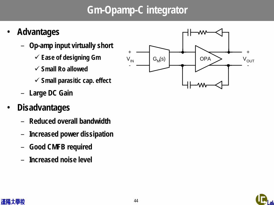
Gm-Opamp-C integrator
• Advantages– Op-amp input virtually short
Ease of designing GmSmall Ro allowedSmall parasitic cap. effect
– Large DC Gain
• Disadvantages– Reduced overall bandwidth– Increased power dissipation– Good CMFB required– Increased noise level
GM(s)+
VOUT-
+VIN-
OPA

45
1st order Gm-C filter
Vin(s)Gm1
+-
Gm2+-
Vout(s)
CA
CX
i1
i2
KCL
( ) ( )( ) 0
01
XA
2m
XA
1m
XA
X
in
outs
ksk
CCGs
CCGs
CCC
sVsVsH
ω++
⇐
⎟⎟⎠
⎞⎜⎜⎝
⎛+
+
⎟⎟⎠
⎞⎜⎜⎝
⎛+
+⎟⎟⎠
⎞⎜⎜⎝
⎛+
=≡
( )( )
A1
1X
XA02m
XA01m
Ck1
kC
CCGCCkG
−=
+⋅ω=+⋅=
46
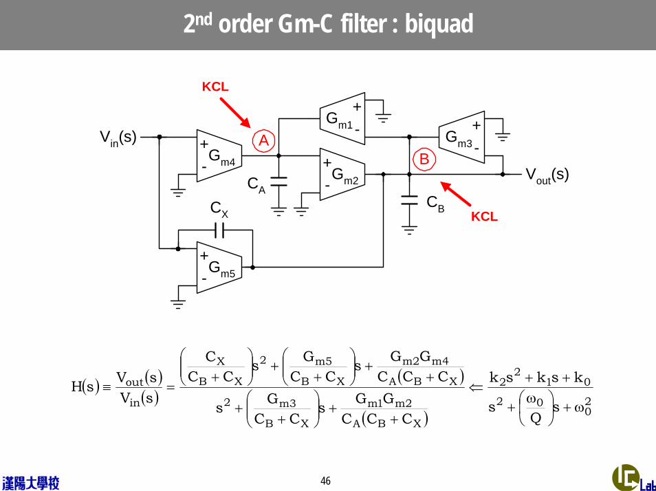
2nd order Gm-C filter : biquad
KCL
Vout(s)Gm2+-
Gm4+-
Gm1+- Gm3
+-
Gm5+-
Vin(s)
CACBCX
AB
KCL
( ) ( )( )
( )
( )20
02
012
2
XBA
2m1m
XB
3m2
XBA
4m2m
XB
5m2
XB
X
in
out
sQ
s
ksksk
CCCGGs
CCGs
CCCGGs
CCGs
CCC
sVsVsH
ω+⎟⎠⎞
⎜⎝⎛ ω+
++⇐
++⎟⎟
⎠
⎞⎜⎜⎝
⎛+
+
++⎟⎟
⎠
⎞⎜⎜⎝
⎛+
+⎟⎟⎠
⎞⎜⎜⎝
⎛+
=≡

47
High-order Gm-C filter with biquads
• 16th order BPF for Japanese PDC– 2 x 8th-order BPF – Average of fo : 450.5kHz– σ of fo : ±1.5kHz– Tuning range of fo : 240~770kHz– 0.35-µm CMOS– Power : 4.8mA @ 2.5V – Active area : 2.5mm2
– Fujitsu ( IEEE ISSCC, 1999)
48
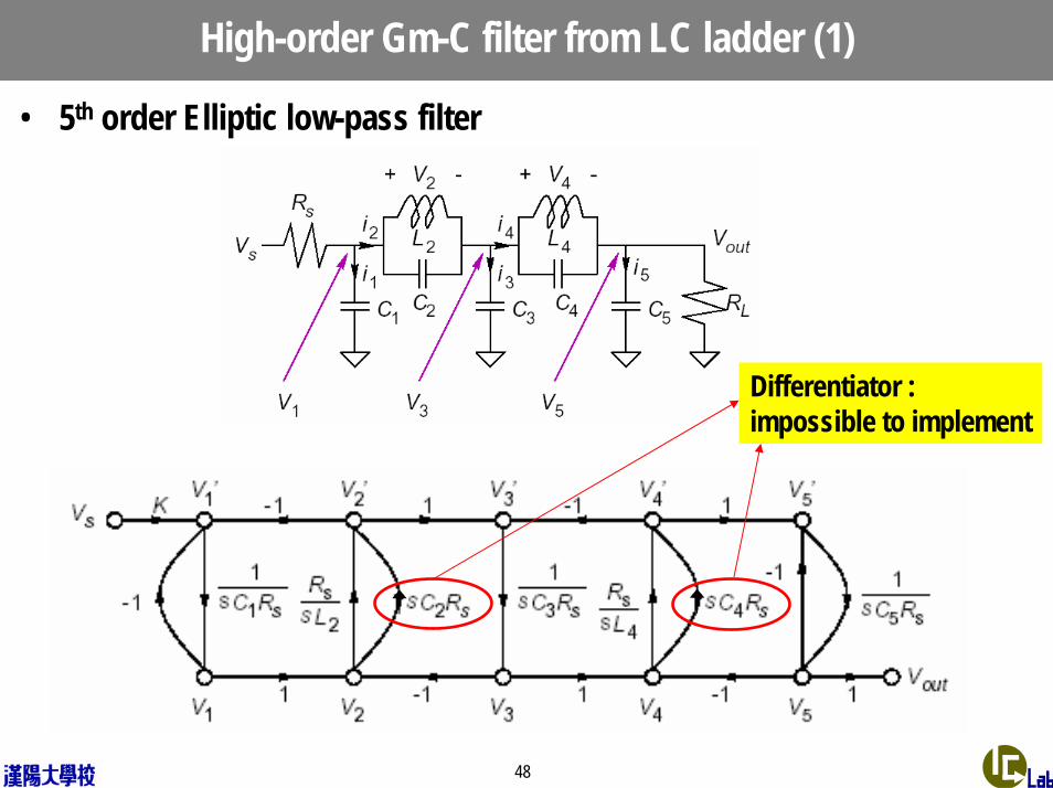
High-order Gm-C filter from LC ladder (1)
• 5th order Elliptic low-pass filter
Differentiator :impossible to implement
49
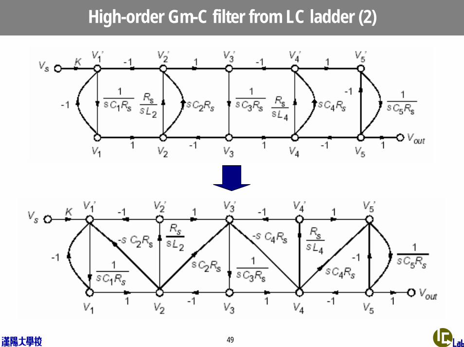
High-order Gm-C filter from LC ladder (2)
50
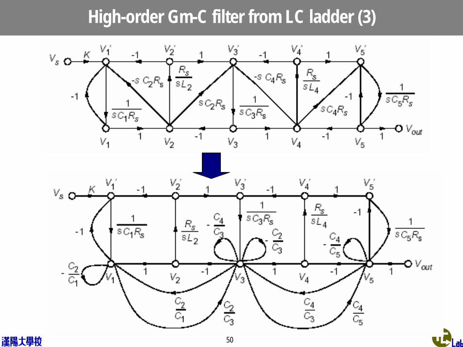
High-order Gm-C filter from LC ladder (3)
51
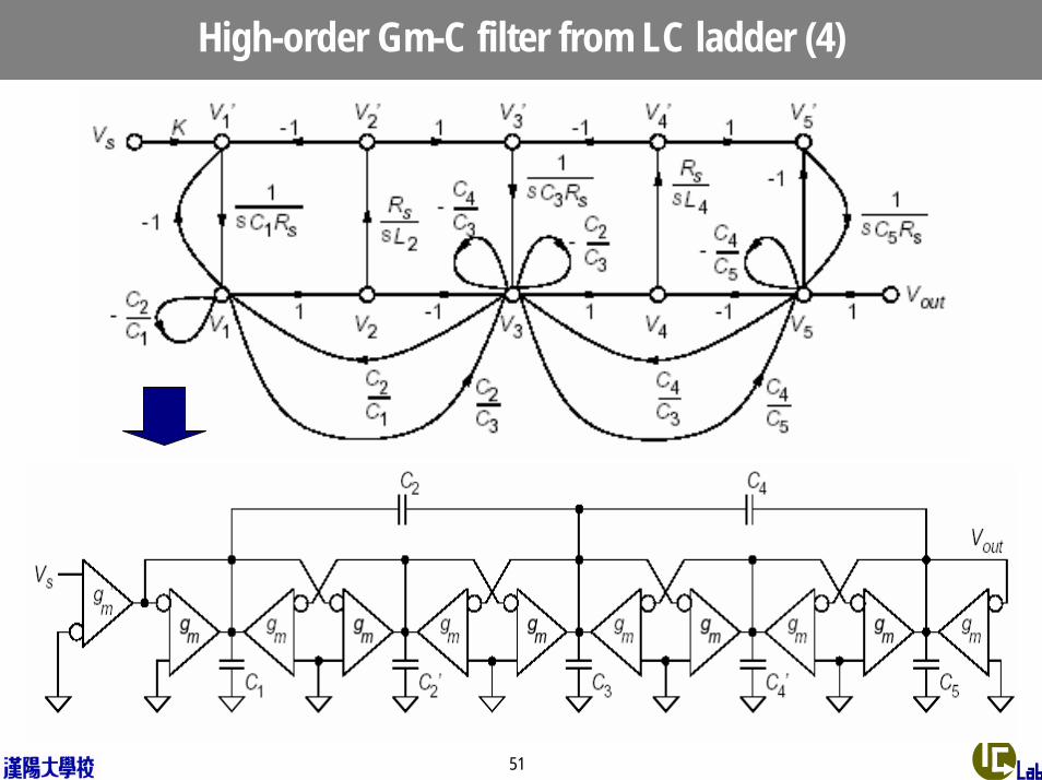
High-order Gm-C filter from LC ladder (4)
52
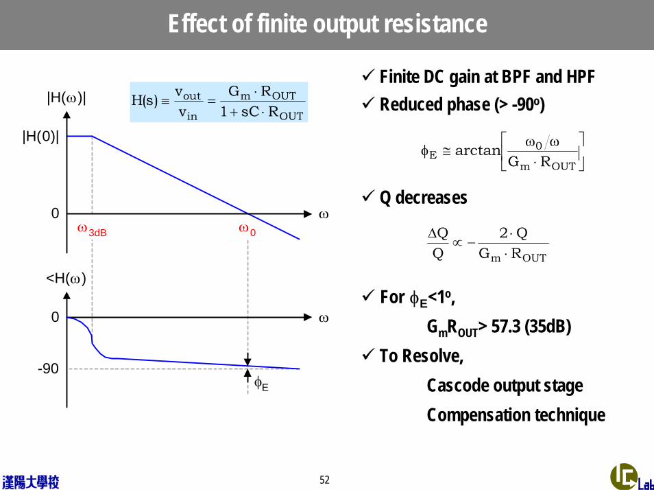
Effect of finite output resistance
Finite DC gain at BPF and HPFReduced phase (> -90o)
Q decreases
For φE<1o, GmROUT> 57.3 (35dB)
To Resolve,Cascode output stageCompensation technique
|H(ω)|
ω
<H(ω)
ω
ω0ω3dB
-90
0
|H(0)|
φE
0
OUT
OUTm
in
outRsC1
RGvv)s(H
⋅+⋅
=≡
⎥⎦
⎤⎢⎣
⎡⋅ωω
≅φOUTm
0E RG
arctan
OUTm RGQ2
⋅⋅
−∝∆

53
Effect of parasitic pole of Gm
Increased Phase (< -90o)
Q increases
For φE<1o, ωp> 57.3 ωo
To resolve,Careful designAdvanced processIntentional zero added
|H(ω)|
ω
<H(ω)
ω
ω0
-90
0
|H(0)|
φE
0
ωP
ω3dB
p
m
in
outs11
CG
vv)s(H
ω+⋅=≡
[ ]pE arctan ωω−≅φ
p
0EQ2
ωω
φ⋅⋅∝∆
54
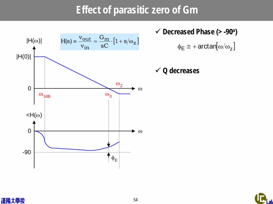
Effect of parasitic zero of Gm
Decreased Phase (> -90o)
Q decreases
|H(ω)|
ω
<H(ω)
ω
ω0ω3dB
-90
0
|H(0)|
φE
0
ωZ
[ ]zm
inout s1
sCG
vv)s(H ω+⋅=≡ [ ]zE arctan ωω+≅φ
IDEC 혼성 모드 시스템 설계 및 실습
Automatic tuning of continuous-time filters
56
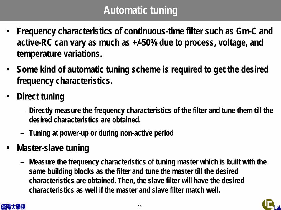
Automatic tuning
• Frequency characteristics of continuous-time filter such as Gm-C and active-RC can vary as much as +/-50% due to process, voltage, and temperature variations.
• Some kind of automatic tuning scheme is required to get the desired frequency characteristics.
• Direct tuning– Directly measure the frequency characteristics of the filter and tune them till the
desired characteristics are obtained.– Tuning at power-up or during non-active period
• Master-slave tuning– Measure the frequency characteristics of tuning master which is built with the
same building blocks as the filter and tune the master till the desired characteristics are obtained. Then, the slave filter will have the desired characteristics as well if the master and slave filter match well.
57
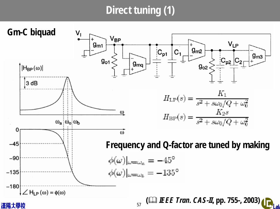
Direct tuning (1)
( IEEE Tran. CAS-II, pp. 755-, 2003)
Gm-C biquad
Frequency and Q-factor are tuned by making
58
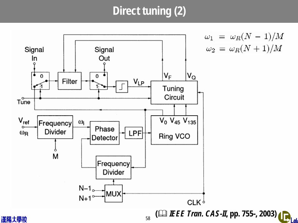
Direct tuning (2)
( IEEE Tran. CAS-II, pp. 755-, 2003)
59
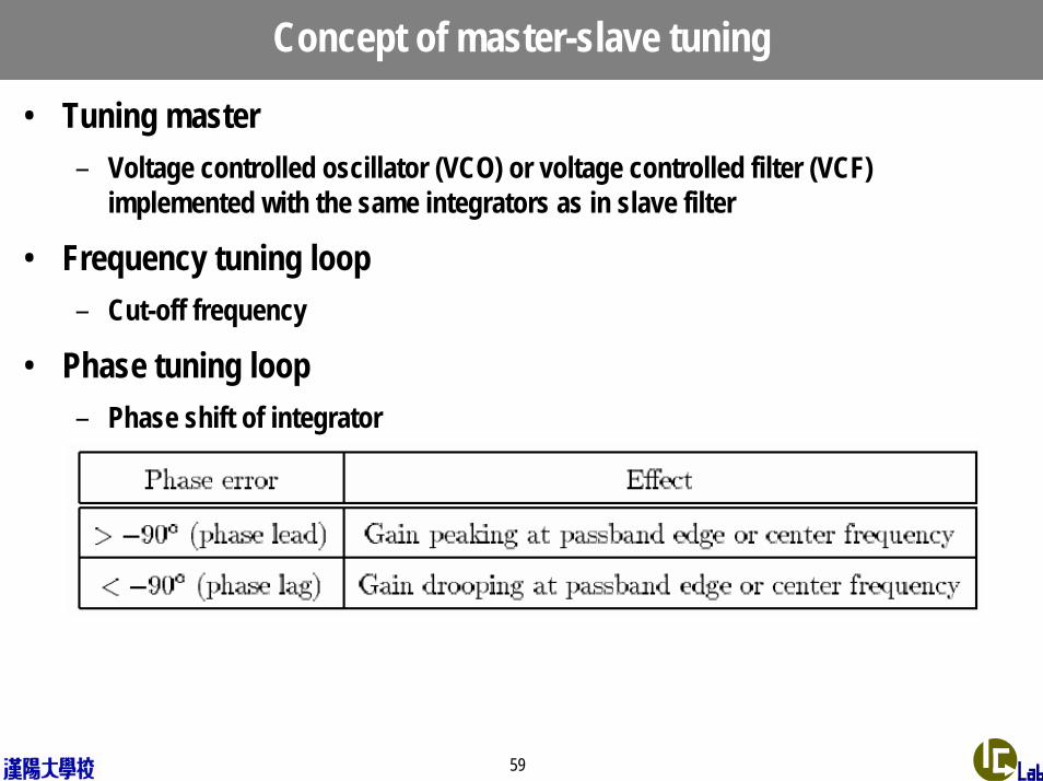
Concept of master-slave tuning
• Tuning master – Voltage controlled oscillator (VCO) or voltage controlled filter (VCF)
implemented with the same integrators as in slave filter
• Frequency tuning loop– Cut-off frequency
• Phase tuning loop– Phase shift of integrator
60
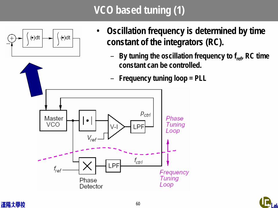
VCO based tuning (1)
• Oscillation frequency is determined by time constant of the integrators (RC).– By tuning the oscillation frequency to fref, RC time
constant can be controlled.– Frequency tuning loop = PLL
61
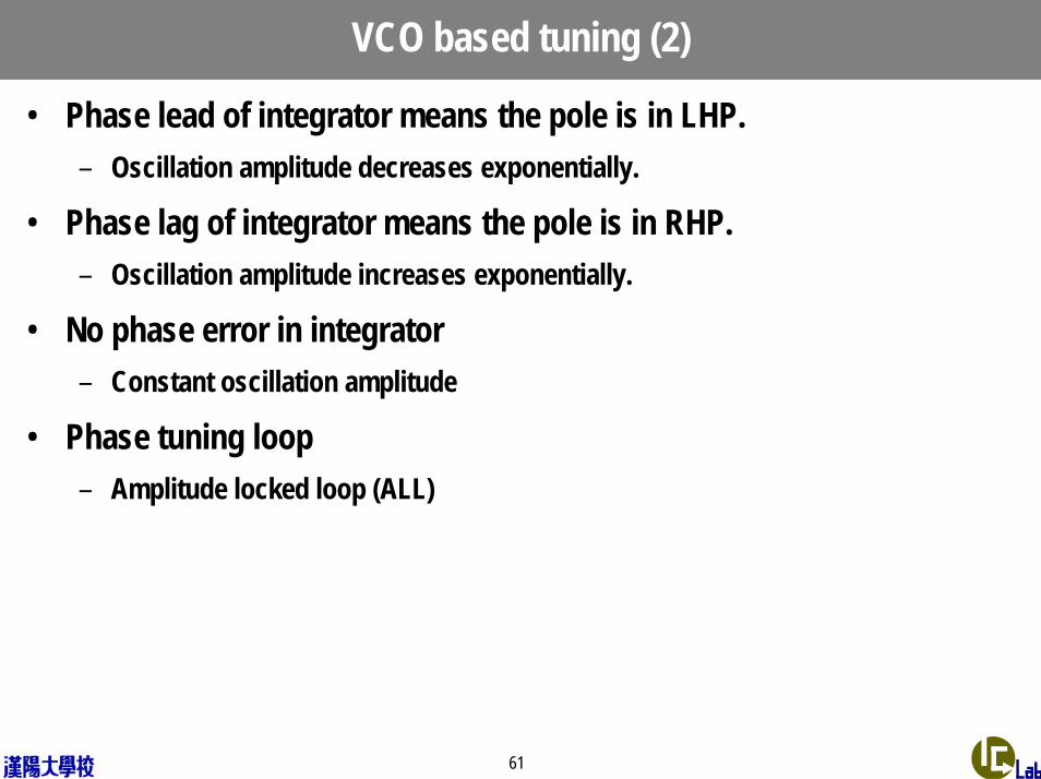
VCO based tuning (2)
• Phase lead of integrator means the pole is in LHP.– Oscillation amplitude decreases exponentially.
• Phase lag of integrator means the pole is in RHP.– Oscillation amplitude increases exponentially.
• No phase error in integrator– Constant oscillation amplitude
• Phase tuning loop– Amplitude locked loop (ALL)
62
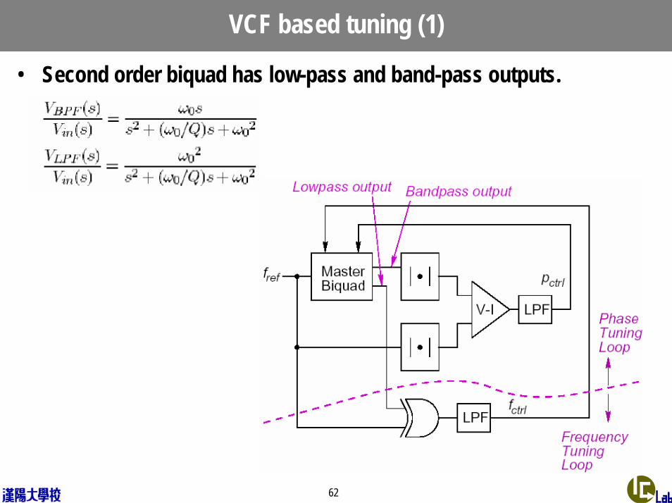
VCF based tuning (1)
• Second order biquad has low-pass and band-pass outputs.
63
VCF based tuning (2)
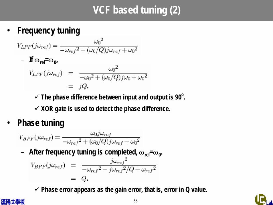
• Frequency tuning
– If ωref=ω0,
The phase difference between input and output is 90o.XOR gate is used to detect the phase difference.
• Phase tuning
– After frequency tuning is completed, ωref=ω0.
Phase error appears as the gain error, that is, error in Q value.
64
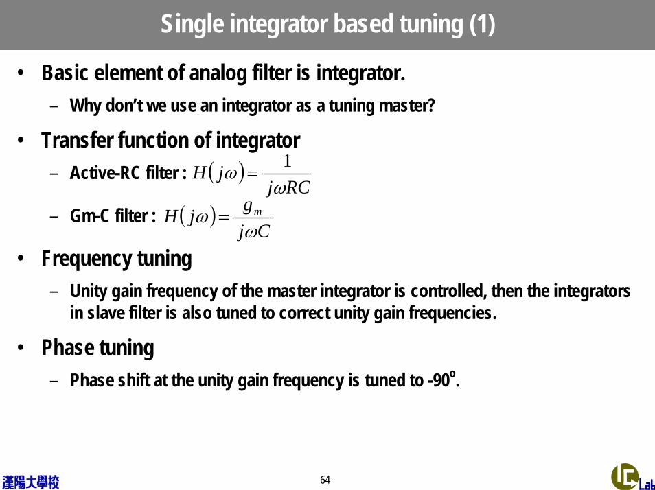
Single integrator based tuning (1)
• Basic element of analog filter is integrator.– Why don’t we use an integrator as a tuning master?
• Transfer function of integrator– Active-RC filter :
– Gm-C filter :
• Frequency tuning– Unity gain frequency of the master integrator is controlled, then the integrators
in slave filter is also tuned to correct unity gain frequencies.
• Phase tuning– Phase shift at the unity gain frequency is tuned to -90o.
( )RCj
jHω
ω 1=
( )Cj
gjH m
ωω =
65
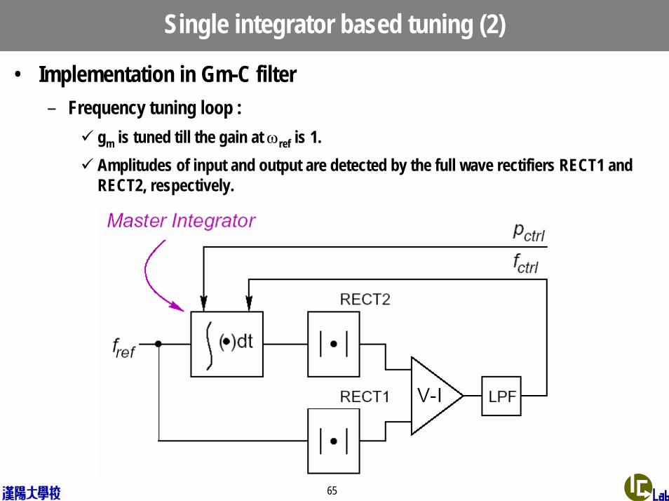
Single integrator based tuning (2)
• Implementation in Gm-C filter– Frequency tuning loop :
gm is tuned till the gain at ωref is 1.Amplitudes of input and output are detected by the full wave rectifiers RECT1 and RECT2, respectively.
66
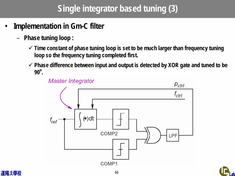
Single integrator based tuning (3)
• Implementation in Gm-C filter– Phase tuning loop :
Time constant of phase tuning loop is set to be much larger than frequency tuning loop so the frequency tuning completed first.Phase difference between input and output is detected by XOR gate and tuned to be 90o.
67
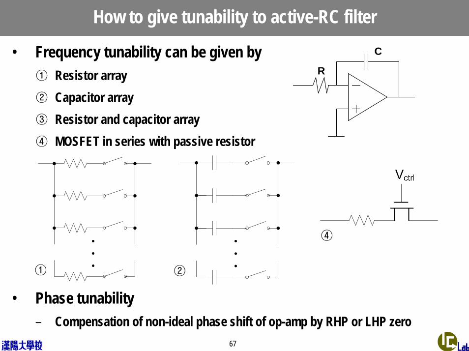
How to give tunability to active-RC filter
R
C• Frequency tunability can be given by ① Resistor array② Capacitor array③ Resistor and capacitor array④ MOSFET in series with passive resistor
• Phase tunability– Compensation of non-ideal phase shift of op-amp by RHP or LHP zero
① ②
④

IDEC 혼성 모드 시스템 설계 및 실습
Design exercise : Active-RC filter

69
Lab. 1 : Synthesis of active-RC filter from passive proto
RS C1 L2 C3 RL
1 1 2 1 1
• Design target– Cut-off frequency = 1.25MHz– Draw a block diagram of fully differential active-RC filter
• Optimize the dynamic range using signal flow graph• For SFG, choose VS, V1, V2’=RS*I2, and V3 as vertex variables.• Set RS=20kΩ.

70
Lab. 2 : Design of fully differential op-amp
• Design target– DC gain > 70dB– Phase margin > 45degree with 5pF load capacitance– VDD=2.5V– Unity gain frequency > 100MHz– CMFB for 1st and 2nd stages
71
Lab. 3 : Design of active-RC filter
• Design a fully differential active-RC filter using the results of lab. 1 and 2.
• See if the frequency characteristic is the same as the passive prototype (of course, except for the cut-off frequency).
• Apply a two-tone sinusoid of 1MHz and 1.25MHz and see the output spectrum.– By varying the input amplitude, you can find the in-band iIP3.
• Apply a two-tone sinusoid of 1.5MHz and 2.5MHz and see the output spectrum.– By varying the input amplitude, you can find the out-of-band iIP3.