Embed Size (px)
Citation preview
UNIVERSITÉ DU QUÉBEC À MONTRÉAL
MODELING AND IMPLEMENTATION OF HIGH PERFORMANCE
MEMS-BASED OSCILLATOR
DISSERTATION PRESENTED
AS PARTIAL REQUIREMENT
TO THE MASTERS IN ELECTRICAL ENGINEERING
BY
ANOIR BOUCHAMI
AUGUST 2017
UNIVERSITÉ DU QUÉBEC À MONTRÉAL Service des bibliothèques
Avertissement
La diffusion de ce mémoire se fait dans le respect des droits de son auteur, qui a signé le formulaire Autorisation de reproduire et de diffuser un travail de recherche de cycles supérieurs (SDU-522 - Rév.1 0-2015) . Cette autorisation stipule que «conformément à l'article 11 du Règlement no 8 des études de cycles supérieurs, [l'auteur] concède à l'Université du Québec à Montréal une licence non exclusive d'utilisation et de publication de la totalité ou d'une partie importante de [son] travail de recherche pour des fins pédagogiques et non commerciales. Plus précisément, [l'auteur] autorise l'Université du Québec à Montréal à reproduire, diffuser, prêter, distribuer ou vendre des copies de [son] travail de recherche à des fins non commerciales sur quelque support que ce soit, y compris l'Internet. Cette licence et cette autorisation n'entraînent pas une renonciation de [la] part [de l'auteur] à [ses] droits moraux ni à [ses] droits de propriété intellectuelle. Sauf entente contraire, [l'auteur] conserve la liberté de diffuser et de commercialiser ou non ce travail dont [il] possède un exemplaire. »
UNIVERSITÉ DU QUÉBEC À MONTRÉAL
MODÉLISATION ET IMPLÉMENTATION D ' OSCILLATEUR MEMS À HAUTES
PERFORMANCES
MÉMOIRE PRÉSENTÉ
COMME EXIGENCE PARTIELLE
DE LA MAÎTRISE EN GÉNIE ÉLECTRIQUE
PAR
ANOIR BOUCHAMI
AOÛT2017

LIST OF FIGURES
LIST OF TABLES
ABSTRACT.
RÉSUMÉ ..
INTRODUCTION
0. 1 Thesis contributions .
CONTENTS
v
IX
xv
. XVII
3
0 .1.1 Non-linear modeling of clamped-clamped MEMS resonator 3
0.1.2 Design of a transimpedance ampli fiers for MEMS-based oscill ators 4
0.2 Thesis outline
CHAPTER I MEMS RESONATOR MODELING
1.1 Introduction . . . . . . .
1.2 Theoretical background .
1.2. 1 MEMS resonator analytical models
1.3 System description .
1.3.1 AHDL mode!
1.3 .2 MEMS oscillator system overview .
1.4 Simulation results . . . . . . . . . . . . . .
1.4.1 MEMS resonator open-loop behavior
1.4.2 Oscillator phase noi se
1.5 Conclusion
CHAPTER II OSCILLATOR BASED ON PIEZOELECTRIC RESONATOR
2.1 Piezoe1ectric di sk resonator overview . . . . . . . . . .
4
7
7
8
9
Il
11
12
13
13
17
19
21
21
IV
2.2 Transimpedance amplifier circuit design
2.2. 1 Input stage . . . . . .
2.2.2 Vari able gain amplifier
2 .2.3 Super source follower
2.2.4 Automatic gain control circuit
2.3 Experimental results . . . . . . .
2.3.1 Resonator characterization
2.4
2.3.2 Transimpedance amplifier characterization
2.3.3 Osc ill ator characterization
Conclusion
CHAPTER III OSCILLATOR BASED ON CAPACITIVE RESONATOR
3.1 Lamé- mode MEMS resonator . .... .
3.2 Transimpedance Amplifier Circuit Des ign
3.3 Experimental Results . . . . . . . .
3.3. 1 Resonator Characterization .
3.3.2 Tran impedance Amplifier Characterization
3.3.3 MEMS Oscillator Characterization .
3.4 Conclusion
22
25
29
30
31
31
32
35
37
44
47
47
49
53
53
56
58
64
CONCLUSION 67
APPENDIX A CMOS CHIP AND CHARACTERIZATION EVALUATION TEST BOARD 69
A. l Printed circuit evaluation board . . ..
A.2 CMOS Transimpedance amplifi er chip
BillLIOGRAPHY . . . . . . . . . . . . . . .
69
69
75
LIST OF FIGURES
Figure Page
1.1 Clamped-clamped bearn resonator diagram (Nabki et al., 2009). 8
1.2 Verilog-A functional diagram. . . . . . . . . . . . . . . . 12
1.3 MEMS-based oscillator with expanded TIA block diagram. 12
1.4 Resonator phase shift at resonance frequency (solid line) and simula-tion elapsed time (dashed line). . . . . . . . . . . . . . . . . . . . . . 15
1.5 (a) Transmiss ion characteristic and (b) di splacement amplitude-frequency curve for various output amplitude levels. . . . . . . . . . . . . . . . 16
1.6 Transmission characteristic for various DC bias voltage levels starting from 6 V to 12 V. . . . . . . . . . . . . . . . . . . . . . . . . . . . . 17
1.7 Start-up response of MEMS-based oscillator in closed-loop for (a) Vp=6V and (b) Vp=IOV. . . . . . . . . . . . . . . . . . . . . . . . . . . . . . . 18
1.8 Phase noise plot for two different DC polarisation voltages with a har-momc noise source. . . . . . . . . . . . . . . . . . . . . . . . . . . . 19
2.1 Simplified diagram of the disk resonator outlining the pads used for differenti ai piezoelectric driving by the TIA and the pads used for elec-trostatic tuning (Eisayed et al., 20 16). . . . . 22
2.2 MEMS-Based Oscillator functional diagram. 23
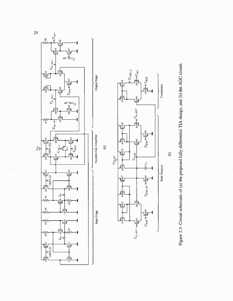
2.3 Circuit schematic of (a) the proposed full y differentiai TIA design , and (b) the AGC circuit. . . . . . . . . . . . . . . . . . . . . . . . . . . . . 24
2.4 Test Setup of the MEMS-based oscillator in open-loop (solid line) and closed-loop (dashed line) with micrographs of the TIA and resonator dies. . . . . . . . . . . . . . . . . . . . . . . . . . . . . . . . . . . . 32
2.5 Normalized transmission characteristic curve for various input ampli-tude levels (a) in air, and (b) under vacuum. . . . . . . . . . . . . . . . 33
VI
2.6 Relative resonant frequency shift of the resonator as a function of the square of the output current in air and under vacuum. . . . . . . . . . 34
2.7 Measured resonator power-handling performance in air and under vac-uum ..................................... 35
2.8 Measured TIA (a) transimpedance gain and (b) 3-dB bandwidth vs.
Vc rRL_A and Vc rRL_BW· . . . . . . . . . . . . . . . . . . . . . . . . 36
2.9 Measured !-dB compression point of the TIA at the maximum transimpedance gain (solid line) and at the oscillation frequency in closed-loop configuration (dashed line). . . . . . . . . . 38
2.10 Measured input-referred current noise of the TIA. 39
2.1 1 Measured open-loop gain and phase shift of the oscillator under vacuum. 40
2. 12 MEMS Osci Il a tor output spectrum. . . . . . . . . . . . . . . . . . . . . 41
2. 13 Measured phase noise of the MEMS-based osci ll ator in air and under vacuum. . . . . . . . . . . . . . . . . . . . . . . . . . . . . . . . . . 42
2.14 Osc illator signal short-time stability for the 14.42 MHz resonator (av-eraged over a five-minute time span) with and without the AGC loop. 43
3.1 Simplified diagram of the (a) exploded and (b) assembled view of the Lamé-mode MEMS resonator with corner supports (Elsayed & Nabki, 2017). . . . . . . . . . . . . . . . . . . . . . . . . . . . . . . . . . . . 48
3.2 SEM micrograph of the Lamé-mode MEMS resonator with corner sup-ports (Eisayed & Nabki, 20 17). . . . . . . . 48
3.3 MEMS-Based oscillator functional diagram. 49
3.4 Circuit schematic of (a) the proposed fully differentiai TIA design , and (b) the AGC circuit. . . . . . . . . . . . . . . . . . . . . . . . . . . . 50
3.5 Simplified equivalent circuit of the RGC input stage used for noise anal-ysis . . . . . . . . . . . . . . . . . . . . . . . . . . . . . . . . . . . . . 52
3.6 Test setup of the MEMS-based oscillator in open-loop (sol id !ines) and closed-loop (dashed !ines) with micrographs of the TIA and resonator. 54
3.7 Normalized resonator transmiss ion characteristic curves for various out-put input amplitude levels for (a) V71 = 100 V and (b) V 71 = 200 Y. . . . . 55
V li
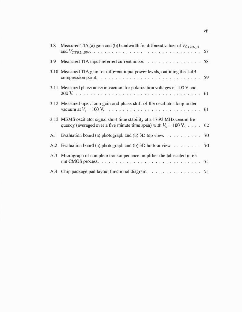
3.8 Measured TIA (a) gain and (b) bandwidth for different values of VcrRL_A and VcrRL_BW · . . . . . . . . . . . . . . . 57
3.9 Measured TIA input-referred current noise. 58
3.10 Measured TIA gain for different input power levels, outlining the 1-dB compression point. . . . . . . . . . . . . . . . . . . . . . . . . . . . 59
3. 11 Measured phase noise in vacuum for polarization voltages of 100 V and 200 V. . . . . . . . . . . . . . . . . . . . . . . . . . . . . . . . . . . 61
3 .1 2 Measured open-loop gain and phase shift of the oscillator loop under vacuum at Vp = 100 V. . . . . . . . . . . . . . . . . . . . . . . . . . 61
3.13 MEMS oscillator signal short time stability at a 17 .93 MHz central fre-quency (averaged over a five minute ti me span) with v;} = 100 V. 62
A.l Evaluation board (a) photograph and (b) 30 top view. . . 70
A.2 Evaluation board (a) photograph and (b) 30 bottom view. 70
A.3 Micrograph of complete transimpedance amplifier die fabricated in 65 nm CMOS process. . . . . . . . . . . . . . . 71
A.4 Chip package pad layout functional diagram. 71

LIST OF TABLES
Table Page
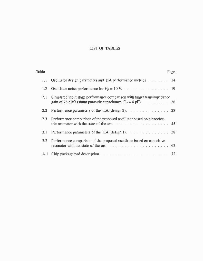
1. 1 Oscillator design parameters and TIA performance metrics 14
1.2 Oscillator noise performance for Vp = 10 V. . . . . . . . . 19
2. 1 Simulated input stage performance comparison with target trans impedance gain of 78 dBD (shunt parasitic capacitance Cp = 4 pF). 26
2.2 Performance parameters of the TIA (design 2). 38
2 .3 Performance comparison of the proposed osci ll ator based on piezoelec-tric resonator with the state-of-the-art. . . . . . 45
3.1 Performance parameters of the TIA (design 1 ). 58
3.2 Performance comparison of the proposed oscillator based on capacitive resonator with the state-of-the-art. 63
A. t Chip package pad description . . . 72

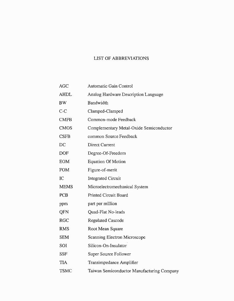
AGC
AHDL
BW
C-C
CMFB
CMOS
CSFB
DC
DOF
EOM
FOM
IC
MEMS
PCB
ppm
QFN
RGC
RMS
SEM
SOI
SSF
TIA
TSMC
LIST OF ABBREVIATIONS
Automatic Gain Control
Analog Hardware Description Language
Bandwidth
Clamped-Ciamped
Common-mode Feedback
Complementary Metai-Oxide Semiconductor
common Source Feedback
Direct Current
Degree-Of-Freedom
Equation Of Motion
Figure-of-merit
Integrated Circuit
Microelectromechanical System
Printed Circuit Board
part per million
Quad-Flat No-leads
Regulated Cascode
Root Mean Square
Scanning Electron Microscope
Sil icon-On-Insulator
Super Source Follower
Transimpedance Amplifier
Taiwan Semiconductor Manufacturing Company

Xli
VGA Variable Gain Amplifier
VNA Vector Network Analyzer
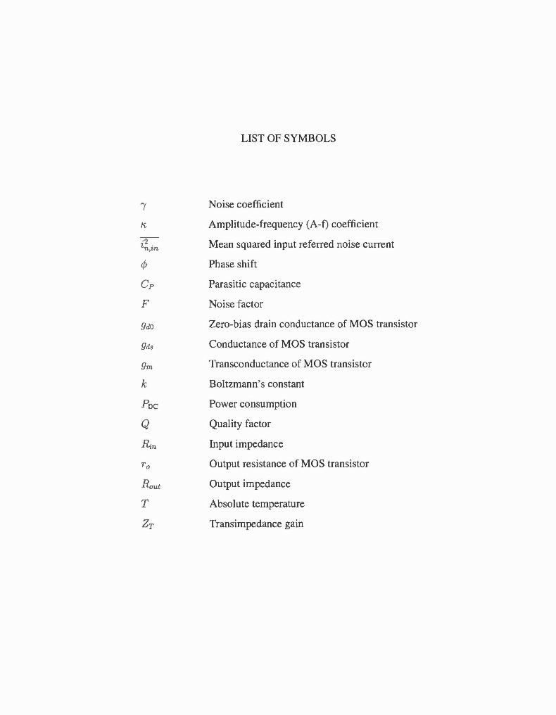
Î
K,
-.2-'/,n ,i n
9dO
9ds
9m
k
Poe
Q
T
LIST OF SYMBOLS
Noise coefficient
Amplitude-frequency (A-f) coefficient
Mean squared input refened noi se current
Phase shift
Parasitic capacitance
Noise factor
Zero-bias drai n conductance of MOS transistor
Conductance of MOS transistor
Transconductance of MOS transistor
Boltzmann's constant
Power consumption
Quality factor
Input impedance
Output resistance of MOS transistor
Output impedance
Absolute temperature
Transimpedance gain

ABSTRACT
The interest in tiny timing applications has been increased over the past decade with regard to an integrated reference oscillator which can offer same performance as oscillators based on quartz crystal. Microelectromechanical systems (MEMS) are considered as a good candidate that can have advantages regarding size scaling and integration with other fabrication processes at lower cast.
The objective of thi s di ssertation is to real ize a high performance full y differentiai transimpedance amplifier (TIA) for a highly integrated reference oscillator. The purpose of thi s circuit will be of sustaining oscillation from a MEMS resonator in closed-loop. This thesis covers non-linearity effects of MEMS resonator in which a Verilog-A mode! of clamped-clamped (C-C) bearn resonator is presented so that electrical and mechanical non-linearities are exposed with this madel. A MEMS-based oscillator is implemented by incorporating a transimpedance amplifier designed in O. 13 /-Lm with the Verilog-A madel. The phase noi se performance dependance on the resonator non-linear effects and its polarisation voltage are illustrated through simulations. Simulation results confirm that careful design must be applied when MEMS resonators are utilised in arder to ensure that non-linearities and biasing do not significantly deteriorate oscillator performance.
In addition, two designs of fully differentiai transimpedance amplifier are designed in arder to meet the specifications of MEMS oscillators based on piezoelectric and capacitive resonators, respectively, in terms of quality factor and insertion Joss. The TIAs are designed in 65 nm CMOS process to take advantages of larger gain-bandwidth product wither lower power consumption which it can be offered by thi s technology, and thus to offset the resonator lasses and to ensure a small phase shift so that high oscillation frequencies (larger than 20 MHz) can be attained. Furthermore, gain and bandwidth can be adjustable separately and input and output impedances reduction methods are applied to avoid loading the resonator 's quali ty factor at a low powerconsumption cast.
The first design uses a regulated cascade (RGC) topology as an input stage to benefit of higher gain and lower input impedance. Thus, the TIA can provide enough gain and bandwidth to sustain oscillation and compensate the !osses of the capacitive resonators. The proposed TIA consumes 1.4 mA from 1-V supp1y. The measured mid-band transimpedance gain is 80 dBD and the TIA features an adjustable bandwidth with a maximum bandwidth of 214 MHz. The measure input-referred current noise of the TIA
XVI
at mid-band is below 4 pNJHz. The TIA is integrated with the MEMS piezoelectric disk resonator and the oscillator performance in terms of phase noise and frequency stability is reported. The measure phase noise in air and un der vacuum is about - 104 dBc/Hz and - 116 dBc/Hz, respectively, at 1-kHz offset, while the phase noise floor reaches -130 dBc/Hz. The measured short-term stability of the MEMS-based oscillator is ±0.38 ppm.
Finally, the second design presents a novel fully differentiai transimpedance amplifier, using the advantages of the regulated cascode (RGC) and common source active feedback topologies, suitable for oscillators based on piezoelectric resonators. The TIA consumes O. 9 mA from 1-V supply. The measured mid-band transimpedance gain is 98 dBD and the TIA features an adjustable bandwidth with a maximum bandwidth of 142 MHz. The measure input-referred current noi se of the TIA at mid-band is below 15 pNJHz. The measure phase noi se of the oscillator based on Lamé-mode MEMS resonator is about - 120 dBc/Hz at 1-kHz offset under vacuum, white the phase noi se floor reaches - 127 dBc/Hz. The measured short-term stability of the MEMS-based oscillator is ± 0.25 ppm.
Keywords: Transimpedance amplifier, Microelectromechanical system, Oscillator, Capacitive resonator, Piezoelectric resonator.
RÉSUMÉ
Au cours de la dernière décennie, les recherches portant sur les applications à base de référence temporelle ont montré un intérêt ce qui concerne 1 'oscillateur de référence intégré qui peut offrir les mêmes performances que les oscillateurs à base de cristal de quartz. Les microsystèmes électromécaniques (MEMS) sont considérés comme un candidat idéal qui peut avoir des avantages concernant la réduction de taille et l'intégration avec d'autres processus de fabrication à moindre coût.
L'objectif est de réali ser un amplificateur à transimpédance (TIA) entièrement différentiel à haute performance pour un oscillateur de référence intégré. Le but de ce circuit sera de maintenir l'oscillation d ' un résonateur MEMS en boucle fermée. Ce mémoire couvre les effets non linéaires du résonateur MEMS à partir d ' un modèle en langage Verilog-A d' une poutre biencastrée. Ceci permet de modéli ser les effets de non-linéarité électriques et mécaniques. Un oscillateur basé sur le modèle Verilog-A du résonateur est ainsi implémenté avec un amplificateur à transimpédance conçu en 0.13 p,m. La dépendance de la performance du bruit de phase sur les effets non linéaires du résonateur et sa tension de polarisation est illustrée par des simulations. Les résultats de la simulation confirment qu ' une conception soigneuse doit être appliquée lorsque les résonateurs MEMS sont utilisés afin de s'assurer que les non-linéarités et les tensions de polarisation ne détériorent pas considérablement les performances des oscillateurs.
En outre, deux modèles d'amplificateur à transimpédance totalement différentiel sont conçus pour répondre aux spécifications des oscillateurs MEMS à base de résonateurs piézoélectriques et capacitifs, respectivement, en matière de facteur de qualité et de perte d ' insertion. Les amplificateurs sont conçus dans un processus CMOS 65 nm pour profiter des avantages en matière de larges gain et bande passante avec la moindre consommation de puissance offerts par cette technologie, par conséquent, compenser les pertes du résonateur et pour assurer un petit déphasage afin que des fréquences d'oscillation élevées (supérieures à 20 MHz) puissent être atteintes. De plus, le gain et la bande passante peuvent être réglables séparément et des méthodes de réduction des impédances d'entrée et de sortie sont appliquées pour éviter de charger le facteur de qualité du résonateur à faible coût de consommation.
Le premier design utilise une topologie de cascade régulé (RGC) comme étage d 'entrée pour bénéficier d'un gain plus élevé et d ' une impédance d'entrée inférieure. Ainsi, l'amplificateur peut fournir suffisamment de gain et de bande passante pour maintenir
XVIII
1' oscillation et compenser les pertes des résonateurs capacitifs. Le TIA proposé consomme 1.4 mA à partir d ' une alimentation de 1 V. Le gain en transimpédance maximal mesuré est de 80 dBD et leTIA dispose d ' une bande passante réglable avec une bande passante maximale de 214 MHz. La mesure du bruit en courant à 1 'entrée est inférieure à 4 pA/VHz. Le TIA est intégré au résonateur piézoélectrique à di sque et la performance de l'oscillateur en fonction de bruit de phase et la stabilité de la fréquence a été présentée. La mesure de bruit de phase dans l' air et sous vide est d 'environ - 104 dBc/Hz et -116 dBc/Hz, respectivement, à un décalage de 1 kHz, tandis que le bruit de phase de fond atteint -130 dBc/Hz. La stabilité mesurée à court terme de l'oscillateur est ± 0.38 ppm.
Finalement, le deuxième design présente un nouvel amplificateur à tran impédance entièrement différentiel, conçu aux oscill ateurs à base de résonateurs piézoélectriques, et ceci en utili sant les avantages des topologies de cascode régulé (RGC) et de source commune en rétroaction active L'amplificateur consomme 0.9 mA à partir d' une alimentation de 1 V. Le gain maximal en transimpédance mesuré est de 98 dB D et le TIA dispose d ' une bande passante réglable avec une bande passante max imale de 142 MHz. La mesure du bruit en courant à l'entrée est inféri eure à 15 pA/VHz. Le bruit de phase de l' osci ll ateur mesuré est d 'environ - 120 dBc/Hz à décalage de 1 kHz sous vide, tandi s que le bruit de phase de fond atteint - 127 dBc/Hz. La stabi lité mesurée à
court terme de l' osci ll ateur basé sur MEMS est de ± 0.25 ppm.
Mots-clés: Ampli ficateur à transimpédance, Microsystème électromécanique, Osc illateur, Résonateur électrostatique, Résonateur piezoélectrique.
INTRODUCTION
Many electronic deviees found in today's markets, such as transceivers for data trans
fer, storage deviees and portable electronics rel y on timing references to deliver the
performance expected from them. One of the essential components in these deviees is
the quartz crystal, which acts as the master time reference. Severa! advantages have
allowed the quartz crystal to be an excellent choice by the industry for frequency syn
thesis applications. Quality factor, frequency stability and its performance in terms
of phase noi se are the main advantages of crystal oscillators. However, crystal oscil
lators are characterized by having a relatively large size, and are difficult to tightly
integrate with other manufacturing technologies, making their cost and footprint rel a
tively large. Severa) studies over the past decade have shown that oscillators based on
micro-electromechanical (MEM) resonators make them excellent candidates to replace
crystal-based resonators in timing applications. In comparison to quartz oscillators,
MEMS oscillators that are 20% smaller have been commercialized (SiTime Corpora
tion, 20 17). Also, severa) works have developed integration processes of MEM res
onators with CMOS technology (Baltes et al., 2002), enabling a potential for further
size and cost reductions.
Micromachined resonators can be operated through two main widespread actuation
mechanisms: piezoelectric or capacitive. Piezoelectric actuation generally provides
high electromechanical transduction efficiencies and low signal transmission !osses,
resulting in low motional resistances, which is very advantageous as it simplifies the
design constraints of the associated electronic circuitry and results in lower power con
sumption. Also, piezoelectric deviees do not require any DC voltage for operation.
2
However, piezoelectric deviees generally suffer from lower quality factors (Hung &
Nguyen, 2011; Schneider & Nguyen, 2014; Zuo et al., 2010; Gong & Piazza, 2013) ,
which can deteriorate the phase noise of the oscillator. Resonators can a1so be classified
based on their vibration modes as either flexural or bulk mode deviees . Bulk mode de
vices typically exhibit high stiffness, and are consequently Jess prone to thermoelastic
damping and consequently achieve large quality factors, even at atmospheric pressure
(Xie et al., 2008; Clark et al., 2005; Elsayed et al., 20 13b; Lin et al., 2004a; Elsayed
et al. , 201 1; Elsayed et al., 20 13a).
In order to implement an oscillator with a MEM resonator, a transimpedance amplifier
(TIA) needs to be interfaced with the resonator in a positive feedback loop to sustain
a steady-state oscillation by converting the resonator driving current to an output volt
age signal (Nabki et al. , 2009; Lin et al., 2004a) . The sharpness and quality of the
output oscillation is usually determined by the quality factor of the resonator and the
contributed noise of the TIA . To sustain oscillation, it is necessary for the TIA to have
high transimpedance gain due to the resonator insertion Joss caused by it motional re
si tance. Large bandwidth is also required to ensure that the oscillator phase shift at
re onance frequency is around 0°, when the MEMS-based oscillator operates in series
resonance mode (He et a l. , 2009). Furthermore, low input and output impedances are
required to minimize the resonator Q-factor loading. Severa) transimpedance topolo
gies have been reported in the literature for MEMS-based oscillator purposes (Salvia
et al., 2009; Zuo et al., 20 1 0; Nabki & El-Gamal, 2008; Baghelani et al., 20 13 ; Li
et al. , 2015 ; Lavasani et al. , 2015 ; Li et al., 2012; Lavasani et al. , 2011 ; Seth et al. ,
20 12; Lin et al. , 2004b; Sundaresan et al. , 2006; Chen et al. , 20 13 ; Li et al., 20 15 ; Huang
et al., 2008) . While most designs used in (Nabki & El-Gamal , 2008; Baghelani et al.,
20 13; Lavasani et al. , 20 15 ; Li et al. , 20 12) are based on RGC topologies, an invert
ing amplifier topology was proposed in (Zuo et al. , 201 0; Lavasani et al., 20 15). On
the other hand, designs proposed in (Seth et al. , 20 12; Sundaresan et al., 2006; Huang
3
et al., 2008) use an automatic gain control circuit to regulate the oscillation ampli
tude and reduce the resonator mechanical non-linearity effect. A current preamplifier
was also introduced in (Lavasani et al., 20 Il). Furthermore, most TIAs use a single
ended architecture (Li et al., 2015; Lavas ani et al., 2015; Li et al., 20 12) and gain
bandwidth (GBW) product enhancement techniques (Lavasani et al., 2011) so th at TIA
performance in terms of input-referred noise and power consumption will be improved.
However, singled-ended TIAs demonstrate inferior noi se performance to that of fully
differentiai TIAs. Differentiai topologies can benefit of common-mode noi se rejection
and even harmonies rejection, and therefore, are more desired in applications requiring
low noise operation (Carusone et al., 2011 ). However, power consumption of full y dif
ferentiai transimpedance amplifier designs in (Seth et al., 20 12; Chen et al., 20 13) are
higher than single-ended TIAs in (Sundaresan et al., 2006; Li et al. , 20 15 ; Huang et al.,
2008).
0.1 Thesis contributions
This di ssertation focused on the realization of CMOS transimpedance amplifier capable
to interface with series-resonant MEMS oscillator applications. As the result of this
research effort, two micromechanical reference oscillators based on both piezoelectric
and capacitive MEMS resonators are demonstrated. The MEMS resonators presented
here are developed by Dr. Mohannad Y. Elsayed in previous works (Elsayed et al.,
20 16; Elsayed & Nabki , 2017). The major contributions of the work presented in thi s
thesis outlined as follows:
0.1.1 Non-linear modeling of clamped-clamped MEMS resonator
A non-linear analog hardware description language (AHDL) mode) for a clamped
clamped bearn resonator is presented. The model captures the electrical and mechanical
non-linear effects, and accounts for the spring softening and Duffing behavior present
4
in resonators at high drive levels . A trans impedance amplifier is designed in 0.13 /Lm
CMOS to implement and simulate a MEMS-based oscillator incorporating the Verilog
A model.
O. 1.2 Design of a transimpedance amplifiers for MEMS-based oscillators
Detailed study of two transimpedance ampli fiers is presented. This study covered both
frequency and noise analyses in detail. The first transimpedance amplifier is suitable for
oscillators based on capacitive resonators since their motional resistance is high, thus
a sustaining oscillation can be achieved with higher gain. The second transimpedance
amplifier is suitable for oscillators based on piezoelectric resonators. Since the mo
tional resistance of piezoelectric resonators is higher than the capacitive resonators,
despite lower quality factor efficiency, a sustaining oscillation can be achieved with
lower gain. Both TIAs are fully differentiai and fabricated in a Taiwan Semiconductor
Manufacturing Company (TSMC) 65 nm process with high gain-bandwidth product
where tunable gain and bandwidth separately feature is introduced. Finally, the mea
sured performances of MEMS-based oscillators are demonstrated and compared with
state-of-the-art os ci Il a tors.
0 .2 Thesis outline
This thesis is organized in the following manner. Chapter 1 provides an overview of
MEMS-based oscillators. In this chapter a Verilog-A model of clamped-clamped bearn
resonator is presented. The phase noi se performance dependence on the resonator non
linear effects and its DC polarization voltage are illustrated through simulations .
Chapter 2 and Chapter 3 describe the design and optimization of the fully differentiai
high-performance oscillators based on piezoelectric and capacitive resonators, respec
tively. The tapies covered in these chapters include the performances of TIAs in terms
of frequency and noi se responses. The open-loop and closed-loop performances of bath

5
capacitive and piezoelectric micromechanical oscillators are also covered. Finally, de
sign trade-offs and their measured performance are provided including a comparison to
the state-of-the-art.

CHAPTERI
MEMS RESONATOR MODELING
1. 1 Introduction
Reference oscillators are of great interest because of their ubiquitous use in timing
applications and in modern wireless communication deviees. MEMS based oscillators
offer advantages over that of traditional quartz crystal-based oscillators which perform
as the resonant filter in such oscillators. However, MEMS resonators exhibit non-linear
behavior and lower power handling capability in comparison to quartz crystals and are
not as easy to mode! in circuit simulators in order to account for these particularities
(van Beek & Puers, 20 12).
MEMS resonator can be modeled in different ways. Lumped electrically equivalent lin
ear models (i .e., RLC resonators) can be used, but are solely linear and do not directly
account for the variation of the MEMS resonator with bias voltage. On the other hand,
to include the non-linear effects present in MEMS resonators, severa! methods can be
employed. Due of its electromechanical nature, the MEMS resonator exhibits differ
ent electrical and mechanical non-linearities (Agrawal et al., 20 13), and these must be
included in models that allow for the resonator to be faithfully represented in circuit
simulations. Traditionally, finite element methods are used to mode! MEMS deviees.
Unfortunately, such analyses lead to models that cannot be readily used in circuit simu
lators, that do not mode! the resonator non-linearity faithfully, or that are cumbersome
8
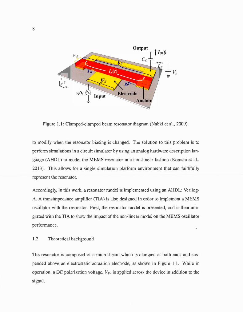
Figure 1. 1: Clamped-clamped bearn resonator diagram (Nabki et al., 2009).
to modify when the resonator biasing is changed. The so lution to this problem is to
perform simulations in a circuit simulator by u ing an analog hardware description lan
guage (AHDL) to mode! the MEMS resonator in a non-linear fashion (Koni shi et al.,
20 13). This allow for a single simul ation platform environment that can faithfully
represent the resonator.
Accordingly, in this work, a resonator madel is implemented us ing an AHDL: Verilog
A. A transimpedance amplifier (TIA) is also designed in arder to implement a MEMS
oscillator with the resonator. First, the resonator madel is presented, and is then inte
grated with the TIA to show the impact of the non-linear madel on the MEMS oscillator
performance.
1.2 Theoretical background
The resonator is composed of a micro-bearn which is clamped at bath ends and sus
pended above an electro tatic actuation electrode, a shawn in Figure 1.1. While in
operation, a OC polarisation voltage, Vp , is applied aeras the deviee in addition to the
signal.
9
1.2.1 MEMS resonator analytical model s
A lumped electrical mode! can be used as a small-signal mode! for the resonator. While
this mode! is a good starting approximation of severa! parameters such as motional
resistance behavior, resonance frequency and quality factor, it ignores electrostatic and
mechanical non-linear effects inherent to the C-C resonator (Van Caekenberghe, 20 12).
The expression of the electrostatic force for a C-C bearn resonator is g iven by
1 [) Fe (X ( t)) = - ~ C (X ( t )) V ( t) 2 ,
2vx ( 1. 1)
where V(t) is the voltage applied across the C-C bearn , composed of a bias and sig
nal voltage, and C(x(t)) is given by ( 1.2), where the fringing capacitance has been
neglected: Eo A
C(x(t))= ()" go+ x t
( 1.2)
In ( 1.2), Eo is the free space permittivity, A is the electrode area, g0 is the actuation
electrode gap and x(t) is the resonator di splacement, later labeled as x for simplicity.
The spring force is traditionally proportional to the di splacement through the linear
spring constant k based on Hooke's law (Senturia, 2000) . However, with a C-C bearn,
the spring force becomes non-linear with sufficiently large bearn displacement and its
expression is given by (Rebeiz, 2004):
( 1.3)
where k1 is the linear spring constant in the spring force given by ( 1.4) and k3 is the
cu bic spring constant given by ( 1.5):
k1 = mw6 , and
k _ 7!.4 E W r tr 3 - 8L3 '
r
( 1.4)
( 1.5)
where E is Young's modulus of structural materi al and Lr, W r and t r are the C-C bearn
resonator dimensions, specifically its length, width and thickness.
,.
10
Constant K is the amplitude-frequency (A-f) coefficient and is an important parameter
to determine if the resonator will exhibit spring softening or spring hardening behavior
(Lee et al., 2011). It is defined as
3 k e3 K = --wo,
8 k el ( 1.6)
where ke1 and ke3 are the effective fundamental and cubic spring constants, respectively,
and are defined as (Mestrom et al., 2009):
v2 k e l = k1 - 2Co-f , and
9o
v2 ke3 = k3- 4Co-f ,
9o
( 1.7)
( 1.8)
where C0 is the overlap capacitance. These take into account the effects of the electro-
static actuation of the resonator on the mechanical spring constants.
The equation of motion (EOM) of the resonator can be mapped to a single degree-of
freedom ( 1-DOF) mass-spring-damper system given by (Mestrom et al. , 2008):
( 1.9)
where a is the acceleration, d is the damping factor and v is the velocity of the mass.
A 1-DOF mode) simplifies the modeling of the resonator, but it must take the reso
nant mode-shape into account to accurately mode) the resonator. For this purpose, the
effective mass and gap capacitance can be rewritten to include the electrostatic force
non-linear effects . These are given by (Lin et a l. , 2004a; Nabki , 201 0)
( 1.10)
C(t) = EoWr , j dl
Le 9o + T(t)Xmode(l) (1.1 1)
where p is the density of the structural material, Le is the electrode length, Xmode is the
bearn mode shape that depends on position lon the bearn and T( t ) is the time function
Il
that describes the position of the bearn during vibration and can substitute x in ( 1.9).
Note that the mode! supports different mode shapes, but only the first C-C mode is
considered here, as it can be readily isolated in single resonator systems.
In response to the resonant motion, an output current is generated and is given by
. d 'lout(t) = dt C(t)V(t) ( 1.12)
1.3 System description
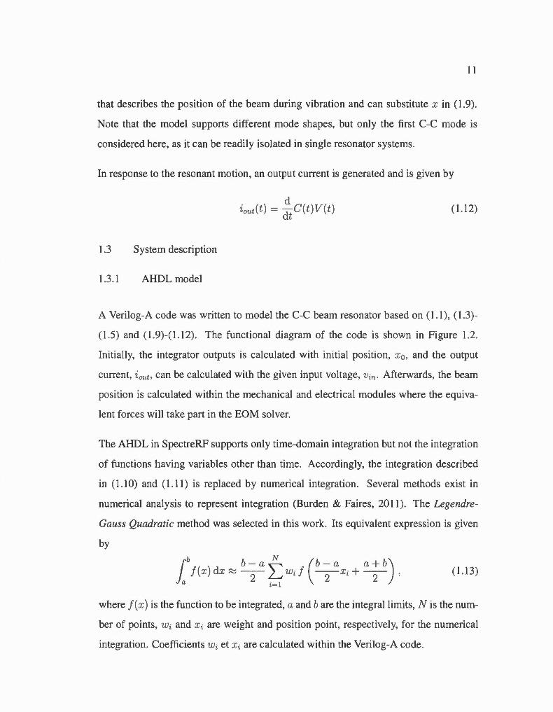
1.3 . 1 AHDL mode!
A Yerilog-A code was written to mode! the C-C bearn resonator based on ( 1.1 ), ( 1.3)
( 1.5) and ( 1.9)-( 1. 12). The functional diagram of the code is shown in Figure 1.2.
Initially, the integrator outputs is calculated with initial position , x 0 , and the output
current, iout. can be calculated with the given input voltage, Vin · Afterwards, the bearn
position is calculated within the mechanical and electrical modules where the equiva
lent forces will take part in the EOM solver.
The AHDL in SpectreRF supports only time-domain integration but not the integration
of functions having variables other than time. Accordingly, the integration described
in ( 1.10) and ( 1.11 ) is replaced by numerical integration. Severa) methods exist in
numerical analysis to represent integration (Burden & Paires, 20 Il). The Legendre
Gauss Quadratic method was selected in thi s work. Its equivalent expression is given
by
b- a b-a a+b b N ( ) 1 f (x ) dx ~ -2
- ~ wi f -2
- xi + -2
- , (1.13)
where J(x) is the function to be integrated, a and b are the integrallimits, N is the num
ber of points, wi and xi are weight and position point, respectively, for the numerical
integration. Coefficients wi et xi are calculated within the Yerilog-A code.
12
V(t)
x(t)
L
Figure 1.2: Verilog-A functional diagram.
1 ---------------------1
1 1
1 iom(l}
1 Out-1
1
1
1
I TIA ~---------------------~
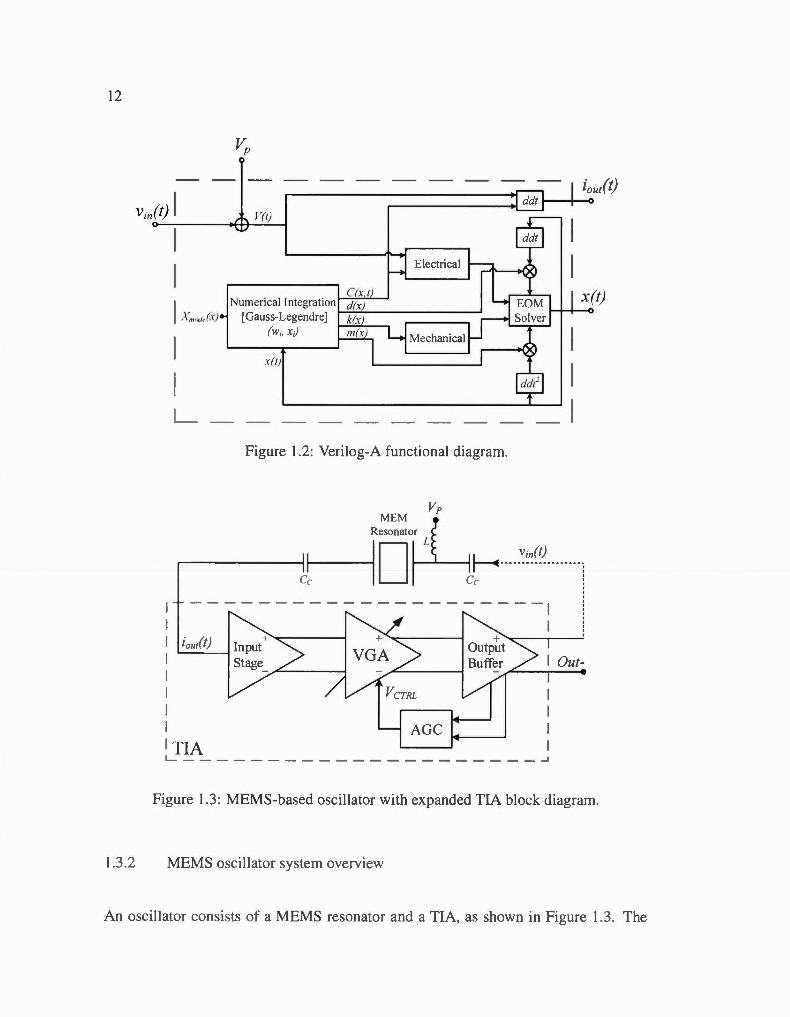
Figure 1.3: MEMS-based oscil lator with expanded TIA black diagram.
1.3 .2 MEMS osci ll ator system overview
An osci ll ator consists of a MEMS resonator and a TIA, as shawn in Figure 1.3. The
- ------------------------
13
TIA was designed in O.l3J.Lm CMOS. To minimize the quality factor loading (Lin et al.,
2004a) , a regulated cascode was used as input stage in order to obtain smaller input
resistance, Rn· An output buffer was also designed in order to obtain smaller output
resistance, R aut · A variable gain amplifier (VGA) alows for the gain of the TIA to
be tuned with voltage V ctrl· The gain of the TIA is controlled by an automatic gain
control (AGC) loop (Nabki & EI-Gamal , 2008) . Note that the polarisation voltage of
the MEMS resonator, Vp, is applied with a bias tee. To sustain oscillation in closed-
1oop, the fo1lowing Barkhausen criteria are required (van Beek & Puers, 20 12; Lin
et al., 2004a):
~riA+ ~AIEA1S = Û0, and
Zr~ R m + R in +Roui ,
( 1.14)
( 1.15)
where ~riA and ~MEMS correspond to the phase shifts of the TIA and resonator, re
spectively, and Zr is the transimpedance gain of TIA. In thi s case, both resonator and
TIA must have 0° phase shift.
1.4 Simulation results
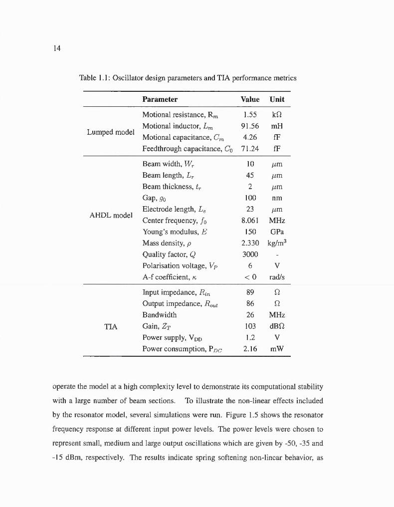
Table 1. 1 summarizes the overall osci11ator circuit design parameters and simulated
TIA performance metrics.
1.4.1 MEMS resonator open-1oop behavior
Before undertaking circuit simulation, the optimal number of points, N, to be included
into the numerical integration block of the Verilog-A model was determined. The num
ber of points used in the integration block is equivalent to dividing the resonator bearn
into equal sections with relative motions characterized by the resonator mode-shape and
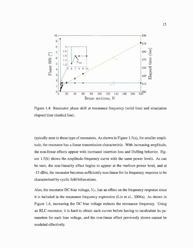
time function. As shown in Figure 1.4, the simulation time is a linear function of N .
The optimal number of sections is attained at Napt = 7 when the phase shift converges
to 1.58°. In this work, simulations were performed with 60 bearn sections in order to
14
Table 1.1: Osci ll ator design parameters and TIA performance metrics
Parame ter Value Unit
Motional resistance, Rm 1.55 kD
Motional inductor, Lm 9 1.56 mH Lumped mode!
Motional capacitance, Cm 4.26 fF
Feedthrough capacitance, C0 71.24 fF
Beam width , Wr 10 J.-Lm
Beam length, Lr 45 J.-Lm
Beam thickness, tr 2 J.-Lm
Gap, go 100 nm
E lectrode length, Le 23 J.-Lm AHDL mode!
Center frequency, Jo 8.06 1 MHz
Young 's modulus, E 150 GPa
Mass density, p 2.330 kg/m3
Quality factor, Q 3000
Po larisation voltage, Vp 6 v A-f coefficient, "' < 0 radis
Input impedance, R n 89 D
Output impedance, R aut 86 D
Bandwidth 26 MHz
TIA Gain, Zr 103 dBD
Power supply, V 00 1.2 v Power consumption, P D C 2.16 mW
operate the mode! at a high complexity leve! to demonstrate its computational stability
with a large number of beam sections. To illustrate the non-linear effects included
by the resonator mode!, severa! simulations were run . Figure 1.5 shows the resonator
frequency response at different input power levels. The power levels were chosen to
represent small, medium and large output oscillations which are given by -50, -35 and
-15 dBm, respectively. The results indicate spring softening non-linear behavio r, as
15
10 530
9 ' ' 510
8 2 ' ' '
' ' ,.---._
,.---._ 7 0 ,____. 0 6 ......... @ 5
::..> :n
4 ('j ...... ........
P-. 3
2
1.8 ' ' ' '
' '
1.6 ' '
~~~OpL ' ' -1.4 ' ' .
' ' ' '
' 1.2 ' ' ' ' v 6 1 8 g ,_o _____
'' -·' '' .-'
'' {
490 :n 6 ,____. ::..>
470 6 . ...... ~
450 '""T;j ::..> :n o.
430 ro --<
lÏI
~- - . -1
410
• 0o 20 40 6o 8o wo 120 140 160 180 2oa
90
Bearn sections N '
Figure 1.4: Resonator phase shift at resonance frequency (solid line) and simulation
elapsed time (dashed line) .
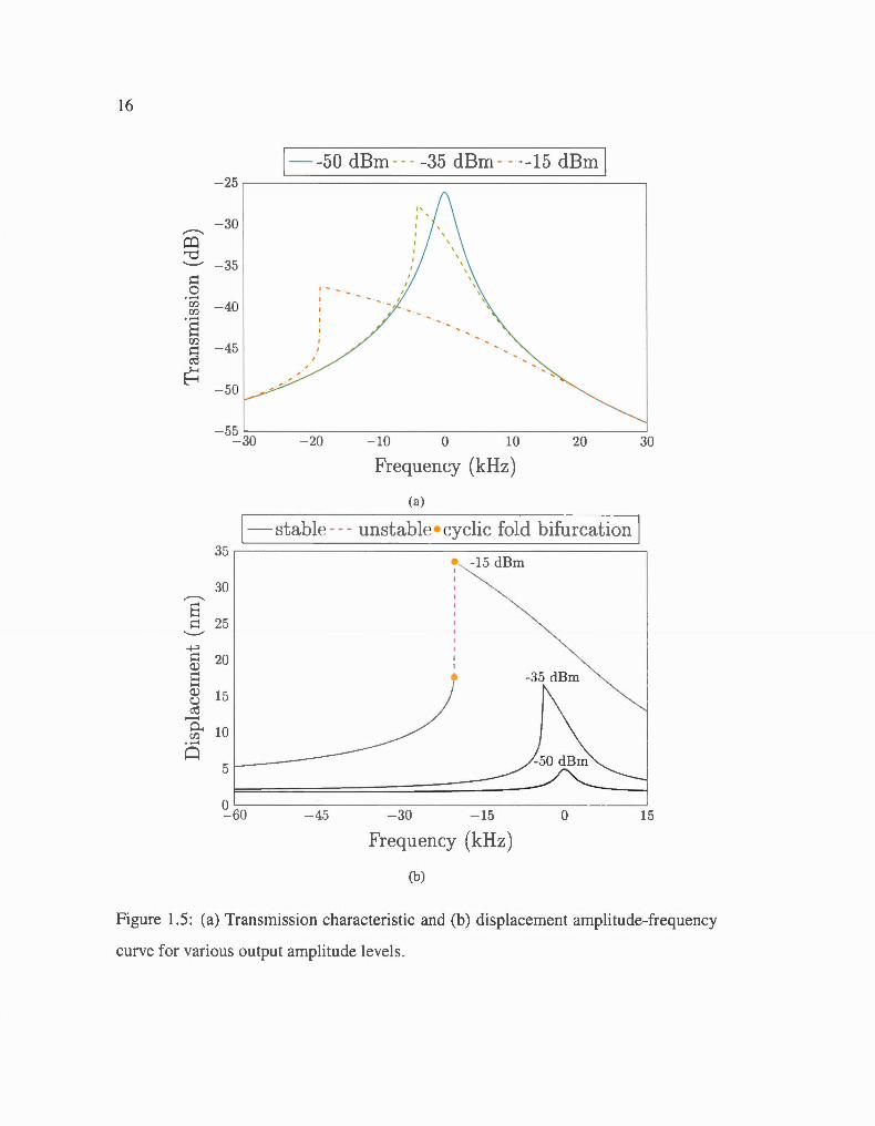
typically seen in these type of resonators. As shown in Figure 1.5(a), for smaller ampli
tude, the resonator has a linear transmission characteristic. With increasing amplitude,
the non-linear effects appear with increased insertion Joss and Duffing behavior. Fig
ure 1.5(b) shows the amplitude-frequency curve with the same power levels. As can
be seen, the non-linearity effect begins to appear at the medium power leve!, and at
-15 dBm, the resonator becomes sufficiently non-linear for its frequency response to be
characterized by cyclic fold bifurcations.
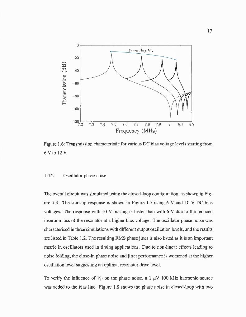
Also, the resonator DC bias voltage, Vp , has an effect on the frequency response since
it is included in the resonance frequency express ion (Lin et al., 2004a) . As shown in
Figure 1.6, increasing the OC bias voltage reduces the resonance frequency. Using
an RLC resonator, it is hard to obtain such curves before having to recalculate its pa
rameters for each bias voltage, and the non-linear effect previously shown cannot be
modeled effectively.
16
1- -50 dBm --- -35 dBm -- --15 dBm 1 - 25
-30 ,_.--...._
~ "'d --.......- -35 p 0 1 - -....... ct:J -40 ct:J
- 1
....... 8 ct:J - 45 p cO
~ - 50
- 55 - 30 -20 - 10 0 10 20 30
Frequency (kHz)
(a)
1-stable --- unstable• cyclic fold bifurcation 1 35
-15 dBm
30 ,_.--...._
8 p 25 --.......-~ p 20 Q)
8 Q) 15 u cO .......... 0.. 10 ct:J . ......
Q 5
~60 - 45 - 30 - 15 0 15
Frequency (kHz)
(b)
Figure 1.5: (a) Transmission characteristic and (b) di sp1acement amplitude-frequency
curve fo r vari ous output amplitude levels.
,---..._
CQ "0 ..____.,
>=1 0 . ...... Cf) Cf) ·a Cf)
>=1 ro ~
0
- 20
-40
- 60
-80
- 100
- 120 L-----------------------------------------~ 7. 2 7.3 7.4 7.5 7.6 7.7 7.8 7.9 8 8.1 8.2
Frequency (MHz)
17
Figure 1.6: Transmission characteristic for various DC bias voltage levels starting from
6 V to 12 V.
1.4.2 Oscillator phase noi se
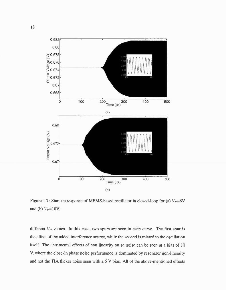
The overall circuit was simulated using the closed-loop configuration, as shown in Fig
ure 1.3 . The start-up response is shown in Figure 1.7 using 6 V and 10 V DC bias
voltages . The response with 10 V biasing is faster than with 6 V due to the reduced
insertion Joss of the resonator at a higher bias voltage. The oscillator phase noi se was
characterised in three simulations with different output oscillation levels, and the results
are li sted in Table 1.2. The resulting RMS phase jitter is also listed as it is an important
metric in oscillators used in timing applications. Due to non-linear effects leading to
noise folding, the close-in phase noise and jitter performance is worsened at the higher
oscillation Jevel suggesting an optimal resonator drive levet.
To verify the influence of Vp on the phase noise, a 1 p, V 100 kHz harmonie source
was added to the bias line. Figure 1.8 shows the phase noise in closed-loop with two
18
0 100
(a)
0 100 200 300 400 500 Time (!J.s)
(b)
Figure 1.7: Start-up response of MEMS-based oscillator in closed-loop for (a) Vp=6V
and (b) Vp= 1 OV.
different Vp values. In this case, two spurs are seen in each curve. The first spur is
the effect of the added interference source, while the second is rel ated to the oscillation
itself. The detrimental effects of non linearity on se noise can be seen at a bias of 10
V, where the close-in phase noise performance is dominated by resonator non-linearity
and not the TIA flicker noise seen with a 6 V bias. Ali of the above-mentioned effects
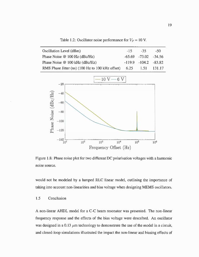
19
Table 1.2: Oscillator noise performance for Vp = 10 V.
Oscillation Leve) (dBm) - 15 -35 -50
Phase Noise@ 100Hz (dBc/Hz) -65.69 -73.02 -34.56
Phase Noise @ 100kHz (dBc/Hz) -119.9 -104.2 -83.82
RMS Phase Jitter (ns) ( 100Hz to 100kHz offset) 6.25 1.51 131.17
I- 10V - 6V I -20~--------~============~--------~
_,.--...,_ N
::r:: -40
-----u c:::l - 60 "'d ....___.,
Q) -80 C/J ....... 0 z
- 100 Q) C/J ro
...c: - 120 o...
- 140 lül
Frequency Offset (Hz)
Figure 1.8: Phase noise plot for two different OC polarisation voltages with a harmonie
noise source.
would not be modeled by a lumped RLC linear model , outlining the importance of
taking into account non-linearities and bias voltage when designing MEMS oscil lators.
1.5 Conclusion
A non-linear AHDL model for a C-C bearn resonator was presented. The non-linear
frequency response and the effects of the bias voltage were described. An oscillator
was designed in a 0. 13 !-lm technology to demonstrate the use of the mode] in a circuit,
and closed-loop simulations illustrated the impact the non-linear and biasing effects of

20
the MEMS resonator on the performance of the MEMS-based oscillator. Ultimately,
the model captures severa) effects such as Duffing behavior or phase noise degradation
when overdriving the resonator that cannot be modeled by a linear model.
CHAPTER II
OSCILLATOR BASED ON PIEZOELECTRIC RESONATOR
2. 1 Piezoelectric di sk resonator overview
The resonator used in this work is presented in (Eisayed et al., 20 16). A brief overview
is given in this section . The resonator is based on a disk structure that is exciting through
piezoelectric actuation . A diagram of the resonator is shown in Figure 2.1. The deviee
is composed of a single-crystalline silicon central di sk structure acting as the main res
onator structure. This di sk is 10 J..Lm thick and has a 200 J..Lm diameter. It is covered by
a 0 .5 J..Lm layer of aluminum nitride (AIN), the piezoelectric material used for transduc
tion. The di sk structure is supported by four suspension beams having a 10 J..Lm width
(the minimum allowed by the design rules of the MEMS fabrication technology) with
90° angular spacing, so as to correspond with the nodal points of the bulk wine-glass
resonance mode. The support beams are anchored to the substrate at their ends and me
chanically connected to the electrical pads. Each of these supports is associated with a
pair of pads, one for the signal routed above the piezoelectric layer, and the other for the
ground, routed through the underlying silicon structural layer. For thi s purpose, an alu
minum layer above the disk structure is patterned into four distinct quadrants, in order
to match the strain distribution and yield differentiai input/output ports. Each electrode
is electrically connected to a distinct signal pad by an aluminum track routed above its
respective suspension bearn. The conductive structural silicon layer itself acts as the
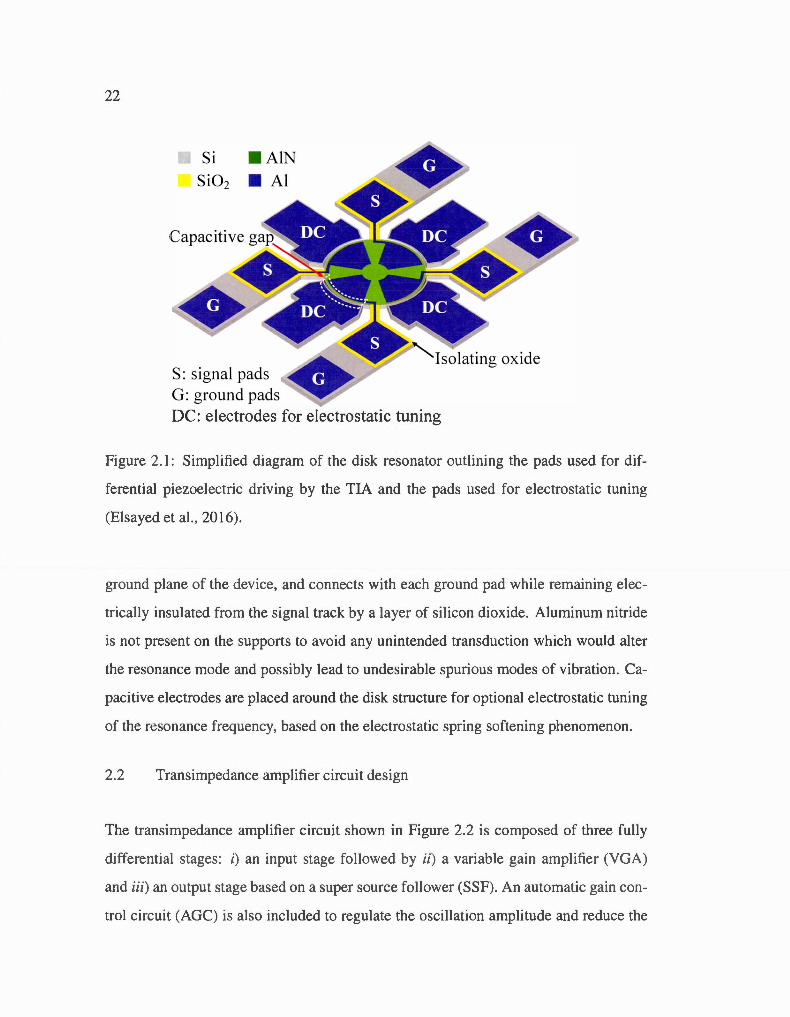
22
Si • AlN Si02 • Al
Capacitive
S: signal pads G: ground pads DC: electrodes for electrostatic tuning
-- -------------
Figure 2.1 : Simplified diagram of the di sk resonator outlining the pads used for dif
ferent iai piezoelectric driving by the TIA and the pads used for electrostatic tuning
(Elsayed et al. , 20 16).
ground plane of the dev iee, and connects with each ground pad while remaining elec
trica lly insulated from the signal track by a layer of silicon dioxide. Alurninum nitride
is not present on the supports to avoid any unintended transduction which would alter
the resonance mode and possibly lead to undesirable spurious modes of vibration. Ca
pacitive electrodes are placed around the disk structure for optional electrostatic tuning
of the re onance frequency, based on the electrostatic spring softening phenomenon.
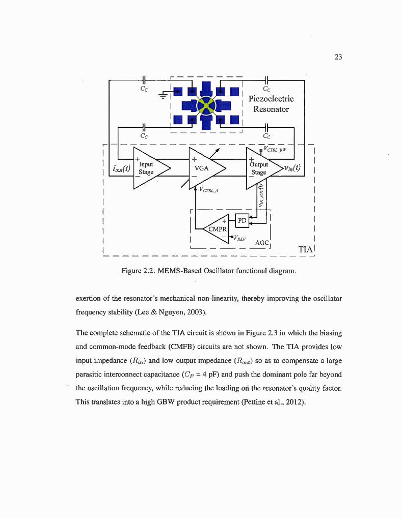
2.2 Transimpedance amplifier circuit design
The transimpedance amplifier circuit shawn in Figure 2.2 is composed of three fully
differentiai stages: i) an input stage fo llowed by ii) a variable gai n ampli fier (VGA)
and iii) an output stage based on a super source follower (SSF). An automatic gain con
trol c ircuit (AGC) is also included to regul ate the oscillation amplitude and reduce the
Cc
Cc
Piezoelectric Resonator
Cc
1
1 in(t) 1
1
1 V REF 1 AGC .___ ______ j
1
1
1
1
1
1
1
TIA I _____________________ __,
Figure 2.2: MEMS-Based Oscillator functional diagram.
23
exertion of the resonator's mechanical non-linearity, thereby improving the oscillator
frequency stability (Lee & Nguyen, 2003).
The complete schematic of the TIA circuit is shawn in Figure 2.3 in which the biasing
and common-mode feedback (CMFB) circuits are not shawn. The TIA provides low
input impedance (~n) and low output impedance (Rout ) so as to compensate a large
parasitic interconnect capacitance (Cp= 4 pF) and push the dominant pole far beyond
the oscillation frequency, while reducing the loading ori the resonator's quality factor.
This translates into a high GBW product requirement (Pettine et al., 20 12).
Inpu
t Sta
ge
Var
iabl
e G
ain
Am
plif
ier
Out
put
Sta
ge
(a)
VoiJ
AG
C
Vcrt
iL_A
Peak
Det
ecto
r C
om
par
a tor
(b)
Fig
ure
2.3:
Cir
cuit
sch
emat
ic o
f (a
) th
e pr
opo
sed
full
y di
ffer
enti
a] T
IA d
esig
n, a
nd (
b) t
he A
GC
cir
cuit
.
25
2.2. 1 Input stage
The input stage should be carefully designed in such a way to satisfy severa! criteria.
Besides the high GBW product criterion, tradeoffs between lower input impedance,
power consumption and current noi se are also other key performance parameters to be
considered when designing the intput stage. Three input stage topologies (Sackinger &
Guggenbuhl , 1990; Salvia et al., 2009; Kopa & Apsel , 2008) were selected to be corn-
pared with the proposed input stage by means of circuit performance simulations using
the SpectreRF simulator in a CMOS 65 nm technology. The first design (Sackinger
& Guggenbuhl, 1990) is based on gm-boosted common-gate (CG) topology, known as
regulated cascode (RGC) input stage and described in (Nabki & El-Gama!, 2008). The
second topology is the common source feedback (CSFB) amplifier presented in (Kopa
& Apsel, 2008). The CSFB technique is used to amplify current, which enhances the
bandwidth by reducing the size of the Joad resistance. The third design considered is
based on (Sa! via et al., 2009), where capacitive feedback is used as a current amplifier.
The input-referred noise of this configuration is expected to be very low because of the
absence of noise sources directly at the input (Razavi , 2000).
Each topology has been simulated with an additional shunt parasitic capacitance of
Cp = 4 pF, and to make a representative comparison of performance, the trans impedance
gain was adjusted to be equal ( '"'-' 78 dBD). A normalized figure-of-merit (FOM1),
which is given by
FONh Gain[D] x BW[A1 H z]
(2. 1) PDc[p,W] x Noise@fo[pA / v'Hz] x R n[D].
FO !Vh is used to evaluate the overall performance of the TIA input stage.
According to Table 2.1, the capacitive feedback topology exhibits the lowest input
referred current noi se, while the CSFB topology exhibits excessive noise. The gain
of the RGC input stage is limited by the large load resistor due to the large DC volt-
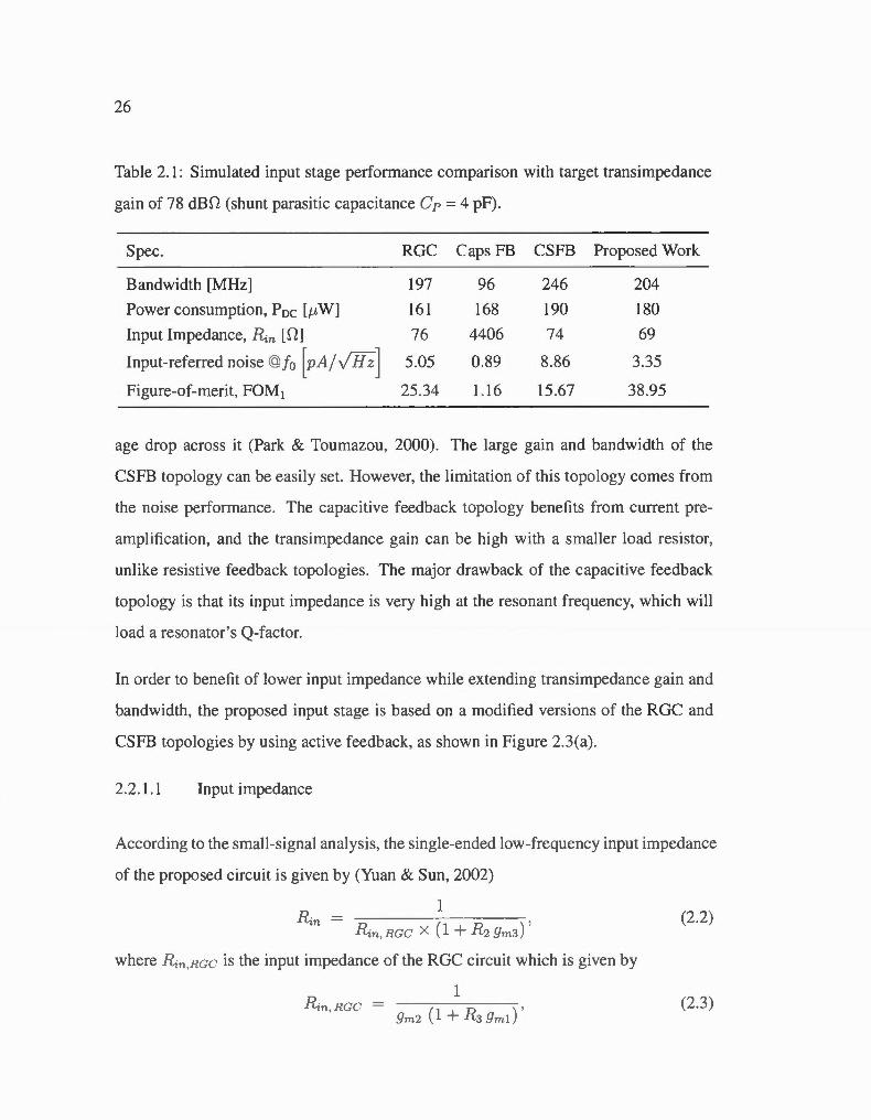
26
Table 2. 1: Simulated input stage performance comparison with target transimpedance
gain of 78 dBD (shunt parasitic capacitance Cp = 4 pF).
Spec. RGC Caps FB CSFB Proposed Work
Bandwidth [MHz] 197 96 246 204
Power consumption, Poe [p,W] 16 1 168 190 180
Input Impedance, ~n [D] 76 4406 74 69
Input-referred noi se @j 0 [pAJ.JHz] 5.05 0.89 8.86 3.35
Figure-of-merit, FOM1 25.34 1.16 15.67 38.95
age drop across it (Park & Toumazou, 2000). The large gain and bandwidth of the
CSFB topology can be easi ly set. However, the li mitation of thi s topology cornes from
the no ise performance. The capacitive feedback topology benefits from current pre
amplification, and the transimpedance gain can be high with a smaller Joad resistor,
un like resistive feedback topologies. The major drawback of the capacitive feedback
topology is that its input impedance is very high at the resonant frequency, which will
Joad a resonator's Q-factor.
In order to benefit of lower input impedance while extending transimpedance gain and
bandwidth , the proposed input stage is based on a modified versions of the RGC and
CSFB topologies by using active feedback, as shown in Figure 2.3(a).
2.2.1.1 Input impedance
According to the small-signal analysis, the single-ended low-frequency input impedance
of the proposed circuit is given by (Yuan & Sun, 2002)
1 ~'Tl= '
~n. RGC X (1 + R2 9m3) (2.2)
where ~n. RGC is the input impedance of the RGC circuit wh ich is given by
1 ~n, R.GC = ( 1 + R ) ,
9m2 3 9m l (2 .3)
27
where 9m1, 9m2 and 9m3 are the transconductance of transistors Ml, M2 and NI3, re
spectively. As indicated by (2.2), the input impedance of the input stage is (1 + R 2 9m3 )
times smaller than an RGC input stage.
2.2.1.2 Transimpedance gain
The expression for the input stage transimpedance gain is given by
where Cn and Cout are the total input and the output capacitances of the input stage,
respectively, C 1 is the equivalent capacitance between the drain of Nil and gate of M2,
C2 is the equivalent capacitance between the drain of NI2 and gate of Jv13/ M 4, and
R o,in is the output impedance of the input stage which is given by R o,in = T 0 4 Il T 0 5,
where T 04 and T 05 are the output resistances of transistors ./III 4 and M 6, respectively.
The OC trans impedance gain is given by
Z (O) ~ R auL 9m4 T , 9m3
(2.5)
where 9 m 4 is the transconductance of transistor NI 4.
2.2.1.3 Bandwidth
It can be seen from (2.4) that the 3-dB bandwidth of the input stage is limited by the
dominant pole appearing at the drain of transi stor M2 and is given by
1 f -3dB ~ ---------------------
[ Cgd2 ( 1 + ~:) + C,,, + Cgd3 + C,d4 9m3 r"' ] , (2.6)
where C9d,i={ 2,3,4} are the gate-drain capacitances of transistors M 2, M 3 and M 4, re
spectively, and C983 is the gate-source capacitance of transistor NI3.
28
The local feedback of the input stage creates a zero at a frequency given by
1 + R 3 9ml ~ 9ml 2n-R3 C1 2nCl.
(2.7)
To keep the zero far away from the dominant pole (Park & Yoo, 2004 ), the transcon
ductance 9ml of transistor Nil should be increased, i.e. increasing its width. However,
increasing the width of M l will significantly increase capacitance C1, specifically the
equivalent capacitance of the drain of Ml, and will reduce the zero frequency. Instead ,
capacitance C 1 can be reduced by reducing the width of transistor N/2 to decrease the
equivalent capacitance at its gate. This will affect the input impedance of the the RGC
stage in (2.3) since the transconductance 9m2 of transistor N/2 will be decreased. How
ever, thi s will not critically affect the input impedance of the RGC stage or the input
stage since 9111 2 is proportional to j(W/ L)2, while its gate capacitance is linearly pro
portional to (W L )2.
On the other hand, decreas ing the input impedance amounts to increas ing (1 + R 2 9m3 )
or (1 + R3 9md · The former will affect the DC TIA gain and the input stage bandwidth.
Therefore, increasing R3 is selected as the method for input impedance reduction .
2.2.1.4 Noise analysis
The input-referred current noise is an important performance parameter to be consid
ered when designing the proposed TIA. lt can be u ed to prov ide a representative com
parison between different circuit topologies (see Table 2.1 ). Since the noi se is most! y
contributed by the input stage, then the noi se of the other stages can be neglected to
simplify the analy i . Therefore, a noi e analy is was carried-out based on the analysis
method proposed in (Park & Yoo, 2004) where shot noi se and flicker noise are ignored.
Assuming that ali noise sources are uncorrel ated, the input-referred cunent noise fo r
29
the input stage is calculated and its expression is given by
(2.8)
where ry is the noise coefficient (Shaeffer & Lee, 1997; Ogawa, 1981 ), k is Boltz
mann 's constant, T the absolute temperature and 9 dO ,i= {l - 6} are the zero-bias drain
conductances of transistors Ml-!11!6 , respectively.
From (2.8), the noi se can be analysed as follow s: the thermal noise and the channel
thermal noi se contributions from R 1 and NI3, respectively, are directly applied to the
equivalent input noise. As the frequency increases, the noise is dominated by terms
containing w2. Therefore, to achieve a low noi se, resistor R 1 need to be increased and
it is preferable to keep the size of transistor M3 as small as possible to maintain lower
input-referred noise as weil as higher transimpedance gain and bandwidth performance.
However, reducing the size of M3 can increase the input impedance of the TIA, as
mentioned earlier, and increasing R3 can compensate the effect of reducing the size of
NI3, thereby achieving an overall compromise of performance.
2.2.2 Variable gain amplifier
The variable gain amplifier shawn in Figure 2.3(a) is based on a differentiai pair am
plifier in which transistors NI1 5 and M 16 form the input pair and M 17 and M18 act
as active loads to provide high gain. The source degeneration transistor M ctrl is used
in the triode region in arder to linearly tune the gain of the VGA over a large range
through control voltage VcrRL_A · Assuming that the output resistance of transistors
30
M14 and M16 are sufficiently large, the gain of VGA can be expressed as
G rv 9ml5 VGA = -gds,ctrl r o l 8 + ,
9ml5 9ds ,ct1'l (2.9)
where r 01s, 9 m 15 , and 9ds,ctrl are the output resistance of transistor M18, transcon
ductance of transistor J\1!15, and the conductance of the source degeneration transistor
M ctrl ' respective) y. Evidently, if r o l 4 and r ol6 are too large and 9ml5 » 9ds,ctrl, the gain
VGA can rewritten as:
GvGA ~ -gds,ctrl r o l 8 ~ -kn ,ctrl ( V as.ctr l - Vth ,ctrl) Tol8 , (2.10)
where k n ,ctr-l, V as.ct1·L, and Vth .ctr-l are the transconductance parameter, gate-source volt
age, and threshold voltage of transistor M ctTL' respectively. Consequently, source de
generation transistor J\!fctrl can linearly control the VGA gain through control voltage
VcrRL_A ·
2.2.3 Super source follower
The output stage shawn in 2.3(a) is based on the SSF topology (Gray et al. , 2009) .
It is based on a differenti ai pair amplifi er in which transistors M20 and M21 form
the input pair and are loaded by the diode connected transistors M22 and M23. The
outputs of the differentiai pair are connected to the AGC circuit for the gain control
loop. The SSF is formed by transistors M24-M29 and resistors R7 and R8 to drive
the fully differentiai resonator and it is characterized by a small output impedance in
arder to avoid loading the resonator 's Q-factor. The gates of transistors M24 and J\1/27
are controlled by control voltage VcrRL_Bw so that TIA bandwidth can be adjusted to
yield the optimal phase loop characteristic.
The gain of the SSF is given by
9 m26 ro26 GssF ~ -------------------------- (2. 11 )
1 1 + 9m26 r o26 + (R Il )
7 ro25 9 m25
31
where 9 m 25 and 9m26 , r 025 and r 026 the transconductances and output resistances of
transistors M25 and M26, respectively. As can be seen in (2.11), if 9m26 r 026 » 1 and
(R7 Il r 025 ) is sufficiently large, the gain of SSF will be close to 1 VN.
The output impedance of the supper source follower is given by
Raut = { (R7 Il To25) Il ( r)(4 ) } ~ 1
, 1 + 9m26 To26 1 + 9m25 r o24 9m26 r o26 9 m25
(2.12)
where r 024 is the output resistance of transistor N/24.
The output resistance of SSF is reduced by a factor of (r026 x 9 m 25 ) in comparison to
the conventional source follower, whose output resistance is ,...._, 1/ 9m· This enhance
ment of the output resistance is due to the negative feedback through transi stor M25.
2.2.4 Automatic gain control circuit
The schematic of the automatic gain control circuit is shown in Figure 2.3(b). The first
stage consists of a differentiai positive peak detector (Wenbo et al. , 20 13) that monitors
the output nodes of the differentiai pair composed of NI20-M21. The peak detector
is based on a differentiai amplifier (11131-M34) and a current mirror (M36 and M37).
Transistor M35 is used a small current sink to discharge capacitor CPD· The peak of the
signal is then compared to an amplitude reference (VREF ), and the resulting difference
is integrated to control the TIA's gain through (VcrRL_A) connected to Mctrl ·
2.3 Experimental results
Two test configuration setups, shown in Figure 2.4, were used to characterize the
MEMS oscillator: i) the open-loop configuration (solid lines) and ii) the closed-loop
(dashed !ines). A Keysight E5061 B vector network analyzer (VNA) was used to mea
sure the two-port S-parameters of the resonator and TIA and as weil as the oscillator in
open-loop in order to obtain the frequency response. The output spectrum and phase
noise of the oscillator were measured with a Keysight N9030A spectrum analyzer.
32
Spectrum Analyzer
0 DOOOOO o ,@-, •co • oo ~ggg ·:
('ô") DOC
.. w~· Bi~~~~~ . 0 v ooo
:G OOOOOO CI O C 0 ODO~ • --- 1
Input Stage
Il
AGC
Output Stage - VGA
iiiiiiiiiiiiiii
1
1
1
Vector Network Analyzer
0 00
Figure 2.4: Test Setup of the MEMS-based oscillator in open- loop (so lid line) and
closed-loop (dashed tine) with micrographs of the TIA and resonator dies.
2.3. 1 Resonator characterization
The frequency response of the resonator was measured in differentiai configuration with
the VNA in air as weil as under a vacuum leve] of 100 mTorr. Different input power
levels starting from - 20 dBm up to 10 dBm were applied to the resonator. Figure
2.5 shows the transmission characteristic curves normalized to the center frequency of
14.42 MHz with a Q-factor of 4900 under vacuum and 1950 in air. The maximum
insertion Joss in air and under vacuum is of - 29 dB and - 22 dB , which corresponds
to a motional resistance of 1.2 kS1 and 0.9 kS1, respectively. Thus, the results indicate
1- -20 dBm --- -10 dBm -- --5 dBm ······ 0 dBm - 10 dBm 1
- 28
- 30
>=:: 0 - 34
"é/3 Cl) ·a - 36 Cl)
@ - 38
~ - 40
- 42 '----...,..-------...,..--------__j -10 -8 - 6 - 4 - 2 0 2 4 6 8 10
Normalized frequency (kHz)
(a)
1--20 dl3m -- - -10 dDm -- --5 dl3m ···· ·· 0 dl3m - 10 dl3m 1
- 20
- 22 ' '
_..---._ - 24 0::)
- 26 '"0
>=:: - 28
0 - 30 "é/3 Cl)
- 32 ·a Cl) -34 >=:: cO - 36 ~ -38
- 40
- 42 - 10 - 8 - 6 - 4 - 2 0 2 4 6
Normalized frequency (kHz)
(b)
33
Figure 2.5: Normalized transmission characteristic curve for various input amplitude
levels (a) in air, and (b) under vacuum .
spring-softening non-linear behavior stemming from the negative amplitude- frequency
(A-f) coefficient (K:) associated with this resonator (Bouchami & Nabki, 2014). The
34
g ill ll.lli:.! 11 .1111 ll .lll li 11 .111" 11.11~
-20
- 40 4 l IH l ('l 1<1<"1 111111
- 60 -- - 1_
-80
41~ - 100 ln a ir
- 120
- 140
- 160 ( 1.11.-, .-, Ill Hi 11 .1 J( .. -, 11 .11( ( 1 11(.-, IJ .Ib
Output current (mA2)
Figure 2.6: Relative resonant frequency shi ft of the resonator as a function of the square
of the output CUITent in air and under vacuum.
amplitude-frequency coefficient can be defined as (Agarwal et al., 2006)
!:lf 1 r ] 2 ' J 0 d
(2.13)
where !:lf / fo is the relative resonant frequency shift and Id is the RMS drive current
through the resonator. From Figure 2.6 the A-f coefficient was calculated in air and
under vacuum to be -45 ppm/mA2 and - 12 ppm/mA2 , respectively ( iller, 198 ).
As can be seen in Figure 2.7, the power-handling capability which conesponds to the
critical vibration amplitude of the resonator was also characterized by measuring its
1-dB compression point (Shao et al., 2008; Kaajakari et al., 2004). The 1-dB compres-
sion points in air and under vacuum were measured to occur at avai lab le input powers
of 5.29 dBm and -5 .1 6 dBm. These are eq uivalent to a 0.32 mA and 0.14 mA RMS
drive current in the resonator, respectively.
--------. o:::l ""d '----"
(/) (/)
0 ..........
>:::: 0 . ...... +" ..... il) (/)
>:::: . ...... ""d il) N . ......
ca s ..... 0 z
1
0
- 1
- 2
- 3
- 4
- 5
- 6
- 7
-8
l- In air --- Under vacuum 1
Pl -dB , a ir = 5.29 dBm
~-~-~-~--~--~--~--~- ~--~--~- ---------;~-'-,,-, -~
Pl-dB, vacuum = -5.16 dBm ',,, '
' ' '
' ' ' '
' \
' '
- 30 - 25 - 20 - 15 - 10 - 5 0 5 10
Input available power ( dBm)
35
Figure 2.7 : Measured resonator power-handling performance in air and under vacuum.
2.3 .2 Transimpedance amplifier characterization
The fully differentiai TIA is fabricated in a TSMC 65 nm low-power process and con
sumes 1.4 mA from a 1-V supply. The circuit active area measures 150 x 220 p,m2 , as
shown in Figure 2.4. To obtain the frequency response of the TIA, S-parameters were
measured usi ng the Keysight E506l B VNA. The network analyzer input power lev el
was set to -45 dBm and the S-parameters were taken from 100 kHz to 1 GHz. The
transimpedance gain (Zr ) is calculated from the S-parameter characteristics as (Weiner
et al., 2003)
521 Zr= Z0 x---
1- Su ' (2.14)
where Z0 represents the 50 D transmission line impedance.
Figure 2.8 shows the transimpedance gain and the 3-dB bandwidth of the TIA, versus
two control signai s, VcrRL_A and VcrRL_Bw. The measured gain reaches ""81 dB D
with bandwidth around 102 MHz extending to 214 MHz when the gain is reduced to
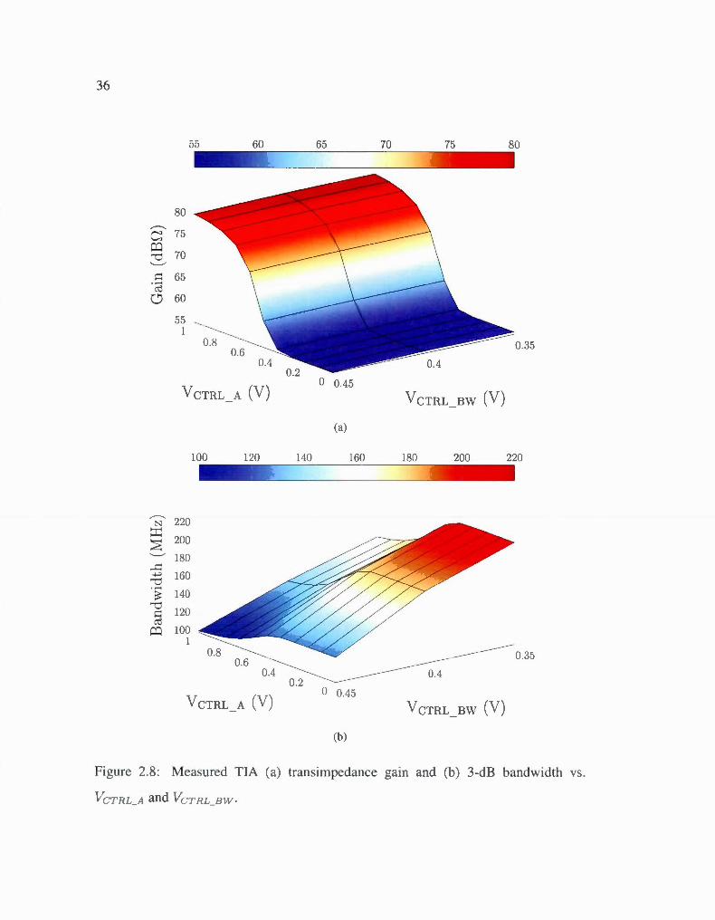
36
80 ...--.... c 75 co
70 '"U ...____...-
>=: 65 '@ 0 60
55 1
0.35
V CTilL A (V) 0 0.45
VcTRL BW (V)
(a)
lOO 120 140 160 180 200 220
...--.... 220 N
::r:: 200 ~ ...____...-
180 ...s:::: ...., 160 '"U ·~
~ 140 '"U
120 >=: cO
co 100 1
0.35
VcTRL A (V) 0 0.45
VcTRL Bw (V)
(b)
Figure 2.8: Measured TIA (a) transimpedance gain and (b) 3-dB bandwidth vs .
Vc rRL_A and VcrRL_BW ·
37
55 dBD. Control voltages can be varied independently. Over the Vc rRL_Bw range, the
maximum gain variation for the same VcrRL_A value is of rv0.2 dB as seen in Figure
2.8(a). The worst case insertion Joss extracted from Figure 2.5 (i.e., Pin=lO dBm in air)
corresponds to a motional resistance equal to 1.7 kD which is corresponding to around
65 dBD. For an input power of -5 dBm the extracted motional resistance is equal to
1.35 kD which corresponds to 62.7 dBD. To overcome the resonator !osses, the maxi
mal transimpedance gain of the sustaining amplifier is fixed to 78 dBD and 170 MHz
bandwidth which is amply sufficient to meet the oscillation conditions (discussed in
section 2.3.3). The AGC loop can then reduce the gain once the oscillation has reached
the appropriate amplitude. The magnitude of the input and output impedances of the
TIA at the resonant frequency of the resonator are 81 D and 100 D, respective! y.
Figure 2.9 shows the measured transimpedance gain at its maximum for different input
power levels varying from -48 dBm to - 20 dBm. A value of available power of
-38.6 dBm was recorded for the 1-dB compress ion point of the TIA.
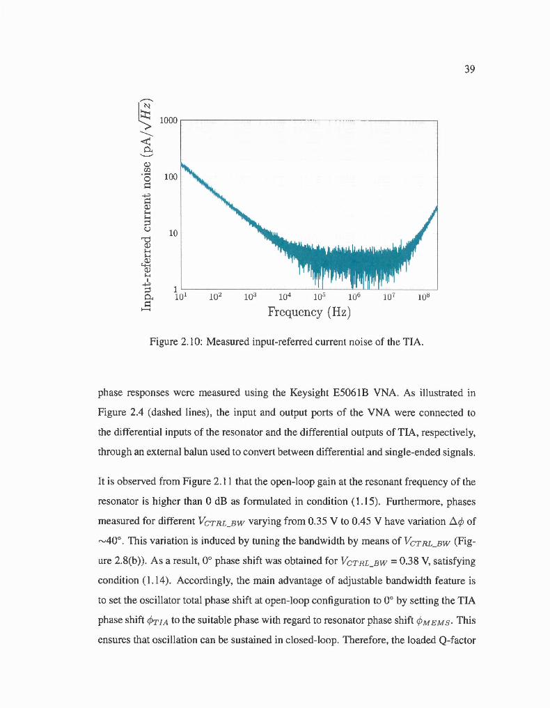
Figure 2.10 shows the input-referred current noi se of the TIA measured with the Keysight
N9030A spectrum analyzer across a 214 MHz bandwidth . At low frequencies , the noise
is dominated by the fticker noise. The flat thermal noise ftoor is seen in the rv20 kHz -
40 MHz frequency range, where the input-referred noise is below 4 pNJHz, then goes
up with a j2 slope because of the gain reduction beyond the bandwidth.
The performance parameters of the TIA configured at the 78 dBD gain-level are sum
marized in Table 2.2.
2.3.3 Oscillator characterization
2.3.3.1 Open-loop measurements
To confirm that sufficient loop gain was present for the oscillation, the resonator was
connected to the TIA in open-loop configuration under vacuum, and the frequency and
38
1- ZT, max --- ZT, closed-loop 1 8 1 ~------~==========~======~------~
79
77 Pl-dB = -38.58 dBm ,.---...
c 75 çq '"0 ~ 73
>=1 "@ 71 CJ P1 -c1 B = -25.65 dBm
69 ------------------------- - -- - -------- \
67
65 8 - 4
-.. - 44 - 40 - 36 - 32 - 28 - 24
Input available power (dBm) - 20
Figure 2.9: Measured 1-dB compression point of the TIA at the max tmum tran
simpedance ga in (so lid tine) and at the oscillation frequency in closed-loop configu
ration (dashed tine).
Table 2.2: Performance parameters of the TIA (design 2) .
Parame ter
Tranimpeande gain [dBO]
Bandwidth [MHz]
Input impedance, R in @Jo [0]
Output impedance, R oui @Jo [0 ]
Power supply, V00 [V]
Power Consumption, Poe [mW]
Input-referred noi se ©fo [pA/.JHz] 1-dB compression point, Pt -dB [dBm]
Active area [mm2]
Pro cess
Measured value
TIA only Closed-loop
78 69
170 158
81 81
!00 !00
1.4 1.4
3.65 10.4
-38 .6 -26.4
0.033
65 nm CMOS
39
1000 ,-----------------------------------------.
100
10
104 105
Frequency (Hz)
Figure 2.10: Measured input-referred current noi se of the TIA.
phase responses were measured using the Keysight E5061 B VNA. As illustrated in
Figure 2.4 (dashed lines), the input and output ports of the VNA were connected to
the differentiai inputs of the resonator and the differentiai outputs of TIA, respective) y,
through an external bal un used to convert between differentiai and single-ended signais.
It is observed from Figure 2.11 that the open-loop gain at the resonant frequency of the
resonator is higher than 0 dB as formulated in condition ( 1.15). Furthermore, phases
measured for different VcTRL_Bw varying from 0.35 V to 0.45 V have variation !::. cp of
'"'..40°. This variation is induced by tuning the bandwidth by means of Vc rRL_Bw (Fig
ure 2.8(b)). As a result, oo phase shift was obtained for VcTRL_Bw ::: 0.38 V, sati sfying
condition ( 1. 14). Accordingly, the main advantage of adjustable bandwidth feature is
to set the oscillator total phase shift at open-loop configuration to oo by setting the TIA
phase shift c/YTI A to the suitable phase with regard to resonator phase shift c/YMEMS· This
ensures that oscillation can be sustained in closed-loop. Therefore, the loaded Q-factor
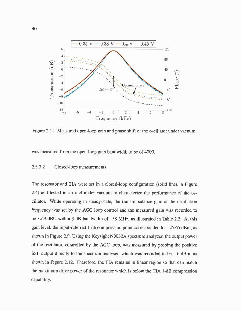
40
6 l- 0.35 V - 0.38 V - 0.4 V - 0.45 V 1
.------===============:::==============---, 120
4 ;------..
2 co 80
-o ..___. 0 40
0::::: 0 - 2 . i) rn
s - 4 rn
-6 0::::: :\l
~ - 8
- 10
- 12 -8 - 6
L__ ______ ------::-------,----,---------,------___j - 120 - 4 - 2 0 2 4 6 8
Frcqucncy (kHz)
Figure 2. 11: Measured open-loop gain and phase shift of the oscillator under vacuum.
was measured from the open-loop gain bandwidth to be of 4000.
2.3.3.2 Closed-loop measurements
The resonator and TIA were set in a closed-loop configuration (solid lines in Figure
2.4) and tested in air and un der vacuum to characterize the performance of the os
cillator. While operating in steady-state, the transimpedance gain at the oscillation
frequency was set by the AGC loop control and the measured gain was recorded to
be rv69 dBD with a 3-dB bandwidth of 158 MHz, as illustrated in Table 2.2. At this
gain level, the input-referred 1-db compression point corresponded to - 25.65 dBm, as
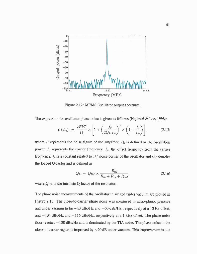
shawn in Figure 2.9. Usi ng the Keys ight N9030A spectrum analyzer, the output power
of the oscillator, controlled by the AGC loop, was measured by probing the positive
SSF output directly to the spectrum analyser, which was recorded to be -6 dBm, as
shawn in Figure 2. 12. Therefore, the TIA remains in linear reg ion so that can match
the max imum drive power of the resonator which is below the TIA 1-dB compression
capabi lity.
,--.....
s o:l -o '----'
H Ill ~ 0 p., ~
;::1 p., ~
;::1
0
0
- 10
- 20
- 30
- 40
- 50
- 60
- 70
-80
14.42
Frequency (M Hz)
Figure 2. 12: MEMS Osc illator output spectrum.
41
The expression for oscillator phase noi se is given as follows (Hajimiri & Lee, 1998) :
2FkT L (jm) = -- X
Po [1 + ( Jo ) 2
x (1 + 1:_)] 2QLJm f m
(2. 15)
where F represents the noi se figure of the amplifier, P0 is defined as the osci ll ation
power, Jo represents the carrier frequency, f m the offset frequency from the carrier
frequency, f e is a constant related to 1/f noise corner of the oscil lator and QL denotes
the loaded Q-factor and is defined as
(2 .16)
where Qu L is the intrinsic Q-factor of the resonator.
The phase noise measurements of the oscillator in air and under vacuum are plotted in
Figure 2.13 . The close-to-carrier phase noise was measured in atmospheric pressure
and under vacuum to be -40 dBc/Hz and -60 dBc/Hz, respective) y at a 10Hz offset,
and - 104 dBc!Hz and - 116 dBc!Hz, respective) y at a 1 kHz offset. The phase noi se
ftoor reaches - 130 dBc/Hz and is dominated by the TIA noise. The phase noi se in the
close-to-carrier region is improved by rv20 dB under vacuum. This improvement is due
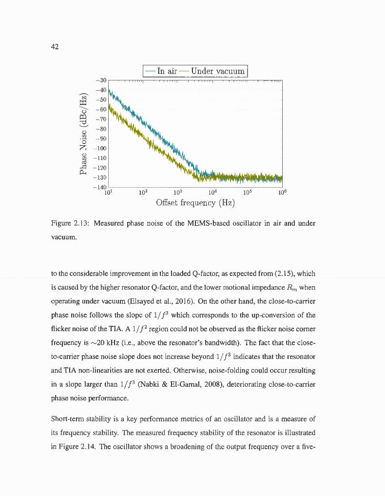
42
l- In air - Under vacuum 1
- 30
- 40 --------N -50 ::r:: -------
- 60 u co - 70 ""Cl '-----" - 80
Q.) en - 90 ·c; z - 100
Q.) - llO en
(1j
...c: P-.
- 120
- 130
- 140 101
Offset frequency (Hz)
Figure 2.13 : Measured phase noi se of the MEMS-based oscillator in air and under
vacuum.
to the considerable improvement in the loaded Q-factor, as expected from (2.15), which
is caused by the higher resonator Q-factor, and the lower motional impedance Rm when
operating under vacuum (El sayed et al. , 20 16). On the other hand, the close-ta-carrier
phase noise follows the slope of 1/ P which corresponds to the op-conversion of the
fi icker noise of the TIA. A 1/ f 2 region could not be observed as the fi icker noi se corner
frequency is r-v20 kHz (i.e., above the resonator 's bandwidth). The fact that the close
ta-carrier phase noise slope does not increase beyond 1 /.J3 indicates th at the resonator
and TIA non-linearities are not exerted. Otherwise, noise-folding could occur resulting
in a slope larger than 1/ P (Nabki & El-Gama!, 2008) , deteriorating close-ta-carrier
phase noise performance.
Short-term stability is a key perfo rmance metrics of an osc ill ator and is a measure of
its frequency stability. The measured frequency stability of the resonator is illustrated
in Figure 2.14. The oscillator shows a broadening of the output frequency over a fi ve-
0
- 5 ,.----... - 10 s 1
1 co - 15 1
'\j -20 ..___.
>--< -25 C,)
~ -30 0 o.. - 35
+=> :::l - 40 o..
- 45 1
+=> :::l
0 - 50
- 55
- 60 -2.5
1--- Overdriven - Controlled with AGC 1
- 2 - 1.5 - 1 -0.5 0 0. 5 1 1.5 2
Normalized frequency (ppm)
1
1 1
1
1
1 1
1 1
1
43
2.5
Figure 2.14: Oscillator signal short-time stability for the 14.42 MHz resonator (aver
aged over a five-minute time span) with and without the AGC loop.
minute time span. The frequency stability is improved from ± 2.1 ppm to ± 0.38 ppm,
when the AGC is used, outlining the importance of not overdriving the resonator.
In order to obtain a representative comparison, a figure-of-merit (FOM) is used to com
pare the performance of the different osci ll ators in terms of phase noise and power
consumption . It is given by (Zuo et al., 201 0)
FOM2 = L(Jm) - 20log (f:.) +lü log ( 1~~) , (2. 17)
where PDc is the OC power consumption of the oscillator circuit in mW. The cal
culated FOM values and summarized specifications for other published MEMS oscil
lators based on piezoelectric resonators are listed in Table 2.3 . As can be seen, the
MEMS oscillator demonstrated in this work has the best figure-of-merit IFüMI when
compared in air and under vacuum to other oscillators based on piezoelectric MEMS
resonators (Pettine et al., 20 12; Ruffieux et al., 201 0; Zuo et al., 201 0; Wu & Rais
Zadeh, 2015; Lavasani et al. , 2012; Lavasani et al., 2015) . Notably, the close-to-carrier
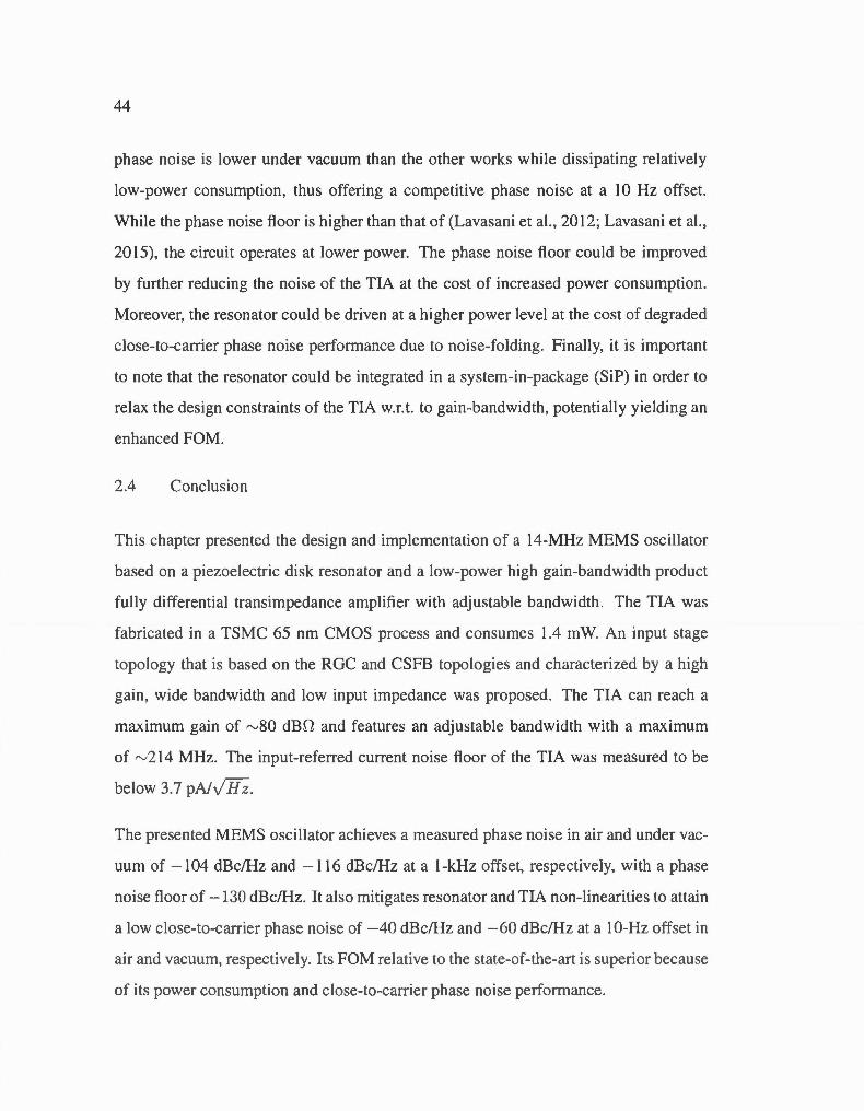
44
phase noise is lower under vacuum than the other works while dissipating relatively
low-power consumption, th us offering a competitive phase noise at a 10 Hz offset.
Wh ile the phase noise floor is higher than that of (Lavasani et al., 20 12; Lavasani et al.,
20 15), the circuit operates at lower power. The phase noise floor could be improved
by further reducing the noise of the TIA at the cost of increased power consumption.
Moreover, the resonator could be driven at a higher power leve) at the cost of degraded
close-to-canier phase noise performance due to noise-folding. Finally, it is important
to note that the resonator could be integrated in a system-in-package (SiP) in order to
relax the design constraints of the TIA w.r.t. to gain-bandwidth , potentially yielding an
enhanced FOM.
2.4 Conclusion
This chapter presented the design and implementation of a 14-MHz MEMS oscillator
based on a piezoelectric di sk resonator and a low-power high gain-bandwidth product
fully differentiai transimpedance amplifier with adjustable bandwidth. The TIA was
fabricated in a TSMC 65 nm CMOS process and consumes 1.4 mW. An input tage
topology that is based on the RGC and CSFB topologies and characterized by a high
gain , wide bandwidth and low input impedance was proposed. The TIA can reach a
maximum gain of "'80 dBD and features an adjustable bandwidth with a maximum
of "'214 MHz. The input-refened current noise floor of the TIA was measured to be
below 3.7 pN.,fJT;.
The presented MEMS oscillator achieves a measured phase noi se in air and under vac
uum of - 104 dBc/Hz and - 1 16 dBc/Hz at a 1-kHz offset, respective! y, with a phase
noise floor of - 130 dBc/Hz. It al so mitigates resonator and TIA non-linearities to attain
a low cl ose-to-carrier phase noi se of - 40 dBc/Hz and -60 dBc/Hz at a 10-Hz offset in
air and vacuum, re pecti vely. It FOM relative to the tate-of-the-art issu peri or because
of its power consumption and close-to-canier phase noi se performance.
Tab
le 2
.3:
Per
form
ance
com
pari
son
of
the
prop
osed
osc
illa
tor
base
d on
pie
zoel
ectr
ic r
eson
ator
with
the
sta
te-o
f-th
e-ar
t.
(Pet
tine
et a
l., 2
012)
(Z
uo e
t al
., 2
010
) (W
u &
Rai
s-Z
adeh
, 20
15)
(Lav
asan
i et
al.,
201
2)
(Lav
asan
i et
al.,
20 15
) T
his
wor
k
CM
OS
tec
hno
logy
0.
35 J
.lm
O.S
J.tm
0.
18J.
tm
O.l8
J.lm
0
.5Jt
m
65 n
m
Cen
ter
freq
uenc
y, J
o [M
Hz]
2
.17
222
78.6
42
7 35
17
5 14
.42
Tes
ting
con
diti
on
air
air
air
air
vacu
um
air
vacu
um
Qu
ality
fac
tor,
Q
450
2100
11
601
1400
18
00
3600
19
52
4894
Mo
tio
nal
resi
stan
ce,
Rr,,
[kS1
] 80
0
03
5
0.05
8 0.
18
1.36
0.
26
1.2
0.9
AG
C c
ircu
it
Y es
N
o N
o N
o N
o Y
es
Pow
er s
upp
ly, V
vo [
V]
3.3
5
1.8
1.8
3
Pow
er c
onsu
mpt
ion,
Po
e [m
W]
1.28
10
4
.8
13
3.8
13.5
1.
4
Pha
se n
ois
e @
1OH
z [d
Bc/
Hz]
-2
5 -2
2 -4
0 -1
0 -5
7 -4
8 -4
0 -6
0
Pha
se n
oise
@1k
Hz
[dB
c/H
z]
-85
-88
-70
-82
-11
2 -1
03
-104
-1
16
Phas
e no
ise
floor
[dB
c/H
z]
-105
-1
60
-122
-1
47
-142
-1
40
-130
-1
30
FO
M2
@lO
Hz
[dB
] -1
21
-159
-1
71
-151
-1
82
-182
-1
62
-182
FO
M2
@!k
Hz
[dB
] -1
51
-185
-1
61
-18
3 -1
97
-197
-1
86
-198

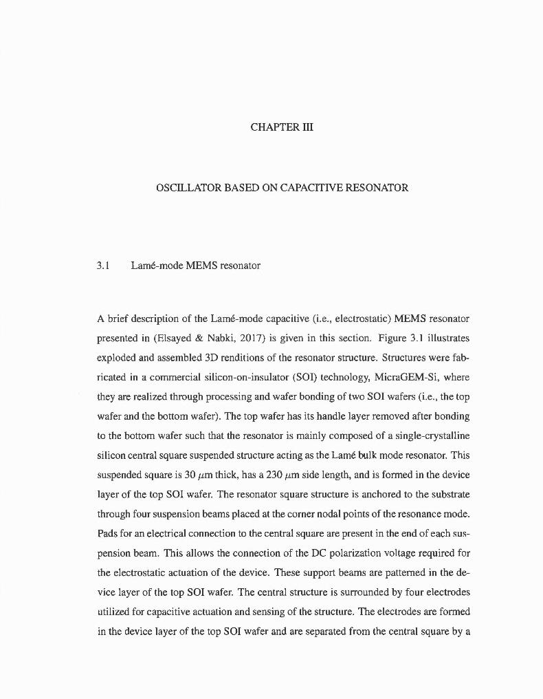
CHAPTER III
OSCILLATOR BASED ON CAPACITIVE RESONATOR
3.1 Lamé-mode MEMS resonator
A brief description of the Lamé-mode capacitive (i.e., electrostatic) MEMS resonator
presented in (Elsayed & Nabki , 20 17) is given in this section. Figure 3.1 illustrates
exploded and assembled 3D renditions of the resonator structure. Structures were fab
ricated in a commercial silicon-on-insulator (SOI) technology, MicraGEM-Si, where
they are realized through processing and wafer bonding of two SOI wafers (i.e., the top
wafer and the bottom wafer) . The top wafer has its handle layer removed after bonding
to the bottom wafer such that the resonator is mainly composed of a single-crystalline
silicon central square suspended structure acting as the Lamé bulk mode resonator. This
suspended square is 30 p,m thick, has a 230 p,m side length, and is formed in the deviee
layer of the top SOI wafer. The resonator square structure is anchored to the substrate
through four suspension beams placed at the corner nodal points of the resonance mode.
Pads for an electrical connection to the central square are present in the end of each sus
pension bearn. This allows the connection of the DC polarization voltage required for
the electrostatic actuation of the deviee. These support beams are patterned in the de
vice layer of the top SOI wafer. The central structure is surrounded by four electrodes
utilized for capacitive actuation and sensing of the structure. The electrodes are formed
in the deviee layer of the top SOI wafer and are separated from the central square by a
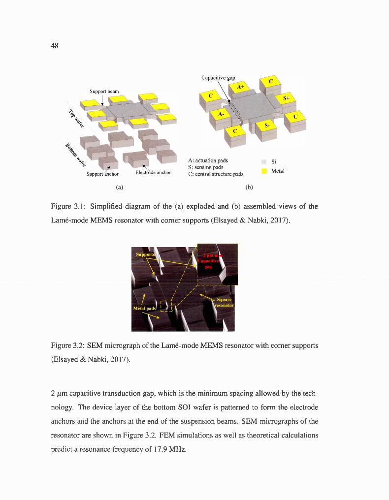
48
(a)
A : actuation pads S: sensing pads C : central structure pads
(b)
Si
Metal
Figure 3. 1: Simplified diagram of the (a) exploded and (b) assembled views of the
Lamé-mode MEMS resonator with corner supports (Elsayed & Nabki , 2017).
Figure 3.2: SEM micrograph of the Lamé-mode MEMS resonator with corner supports
(Elsayed & Nabki, 2017).
2 ~-tm capacitive transduction gap, which is the minimum spacing allowed by the tech
nology. The deviee layer of the bottom SOI wafer is patterned to form the electrode
anchors and the anchors at the end of the suspension beams. SEM micrographs of the
resonator are shawn in F igure 3.2. FEM simulations as weil as theoretical calculations
predict a resonance frequency of 17.9 MHz.
E le ctros tati c Resonator
L__
Cc
--,
1
Vin(l) 1
1
1
1
1
1
1
TIAI
Figure 3.3: MEMS-Based oscillator functional diagram.
3.2 Transimpedance Amplifier Circuit Design
49
The TIA circuit shown in Figure 3.3 is composed of a three fully differentiai stages:
i) an input stage followed by ii) a variable gain amplifier (VGA) controlled by an
automatic gain control circuit (AGC) , and iii) an output stage (super source follower
(SSF)) . The complete schematic circuit is shown in Figure 3.4 in which the biasing and
common-mode feedback (CMFB) circuits are not shown. The sustaining amplifier pro
vides low input impedance (~n) and low output impedance (Raut ) so as to compensate
for large parasitic capacitance (Cp = 4 pF) and push the dominant pole far beyond the
oscillation frequency. This translates into a high gain-bandwidth (GBW) product.
'----y--------->
Inpu
t S
tage
V
a ria
ble
Ga
in A
mp
lifie
r
Peak
Det
ecto
r
Out
put
Stag
e
(a)
Voo
AG
C
Com
para
tor
(b)
Figu
re 3
.4:
Cir
cuit
sch
emat
ic o
f (a
) th
e pr
opos
ed f
ully
dif
fere
ntia
i TIA
des
ign,
and
(b)
the
AG
C c
ircu
it.
Vl
0
51
The gain of the TIA needs to be high enough in order to compensate for the motional
resistance of the MEMS resonator and sustain the oscillation. The regulated cascode
(RGC) topology (Sackinger & Guggenbuhl, 1990) was chosen as input stage to achieve
a reasonable trade-off between gain, bandwidth and power consumption.
The input impedance of the RGC input stage is given by
1
gm2 (1 + R 3 gml) ' (3 . 1)
where gm1 and gm2 are the transconductances of transi stors !VIl and M2, respectively.
Thus, smaller input impedance can be attained by increasing voltage gain of the local
feedback stage given by (1 + R 3 gmd·
The express ion of input stage gain is given by
(3.2)
where Gin• C1, and C9d2 are the total input capacitances of the input stage, the equiv
alent capacitance between the drain of Ml and gate of M 2, and the gate-drain capaci
tance of transistors M2, respective) y. To achieve a higher gain, R2 should be increased,
although it cannot be arbitrarily enlarged because of design constraints.
It can be seen from (3 .2) that the 3-dB bandwidth of the input stage is limited by the
dominant pole appearing at the drain of transistor Nil and is given by
1 1 J -3
dB = 2n-Rl Gin '::::! 2n-Rl X ( Cgsl + Cgdl R 3gmi) ' (3.3)
where C 9d1, C 951 , and C 952 are the gate-drain capacitance of transistor M l, and the
gate-source capacitances of transistors Ml , and N/2, respectively.
52
În.RJ Îll,DI+R3 Ïn.R2
Figure 3.5: Simplified equivalent circuit of the RGC input stage used for noise analysis.
The local feedback of the input stage generates a zero at a frequency of
.fz ~ 2~~~ ~ _ [ ------=-------9ml ( _ ) l 27T C9d1 + C9d2 1 + ~~
(3.4)
To maintain the zero far away from the dominant pole (Park & Yoo, 2004), the gate
drain capac itance of transistor NI2 should be reduced by decreasing its width. In this
fashion, the RGC input impedance in (3.1) will not be dramatically affected since 9m2
will not decrease considerably as it is prop01tional to J (W / L )2, while its gate capaci
tance is linearly proportional to (lill L )2. This can be compensated by increasing R3 as
the input impedance is inverse! y proportional to (1 + R3 9md, as shown in (3.1 ).
The input-referred current noise is a key performance parameter to be considered when
designing the proposed TIA. It can be used to provide a representative comparison
between different circuit topologies. Since the noi se is mostly contributed by the input
stage, the noi se of the other stages can be neglected. Therefore, a noise analysis carried
out using the equi valent c ircuit shown in Figure 3.5, and is based on the analysis method
proposed in (Park & Yoo, 2004), where shot noise and flicker noise are neglected.
Assuming that ali noise sources are uncorrelated, the input-referred cutTent noi se of the
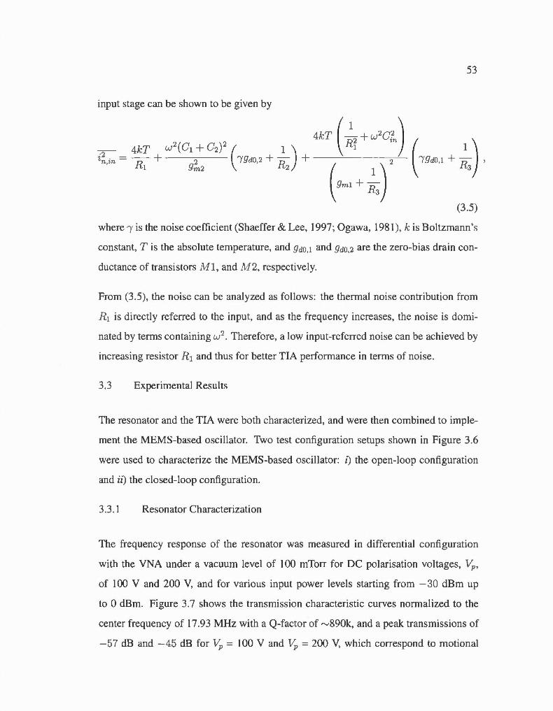
53
input stage can be shown to be given by
(3.5)
where 'Y is the noise coefficient (Shaeffer & Lee, 1997; Ogawa, 1981 ), k is Boltzmann 's
constant, T is the absolu te temperature, and 9do , 1 and 9do,2 are the zero-bias drain con
ductance of transistors Nil, and N/2, respective) y.
From (3.5) , the noi se can be analyzed as follows: the thermal noise contribution from
R1 is directly referred to the input, and as the frequency increases, the noi se is domi
nated by terms containing w 2. Therefore, a low input-referred noi se can be achieved by
increasing resistor R 1 and thus for better TIA performance in terms of noi se.
3.3 Experimental Results
The resonator and the TIA were both characterized, and were then combined to impie
ment the MEMS-based oscillator. Two test configuration setups shown in Figure 3.6
were used to characterize the MEMS-based oscillator: i) the open-loop configuration
and ii) the closed-loop configuration.
3.3.1 Resonator Characterization
The frequency response of the resonator was measured in differentiai configuration
with the VNA under a vacuum leve) of 100 mTorr for OC polarisation voltages, VP,
of 100 V and 200 V, and for various input power levels starting from -30 dBm up
to 0 dBm. Figure 3.7 shows the transmission characteristic curves normalized to the
center frequency of 17.93 MHz with a Q-factor of rv890k, and a peak transmissions of
-57 dB and -45 dB for VP:::: 100 V and VP :::: 200 V, which correspond to motional
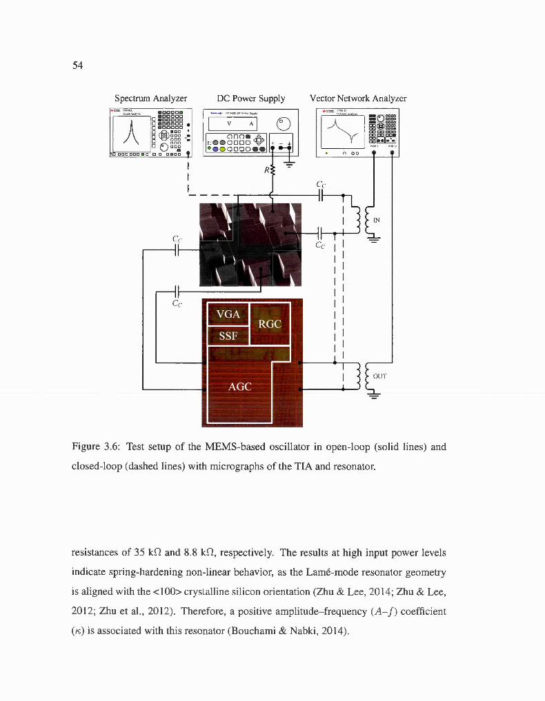
54
Spectrum Analyzer '/»._ :.:'IIOJOA
0 ....... ,.,. 0 588888
0 000000 • 0 000000 o ogo• oo • 0 0 000 • 0 000 .... _
0 ô ggg : a ooo a a a cao~ '
DC Power Supply Vector Network Analyzer
0 00
c::u Cc 1 1
1 1
1 1 1 1 1 1 1 1
1 1
1 1
1 1
1 1 1
Figure 3.6: Test setup of the MEMS-based oscillator in open-loop (so lid Iines) and
closed-loop (dashed lines) with micrographs of the TIA and resonator.
resistances of 35 kO and 8.8 kO, respectively. The results at high input power levels
indicate spring-hardening non-linear behavior, as the Lamé-mode resonator geometry
is aligned with the <100> crystalline silicon orientation (Zhu & Lee, 20 14; Zhu & Lee,
20 12; Zhu et al. , 2012) . Therefore, a posi tive amplitude- frequency (A- f) coefficient
(K;) is associated with thi s resonator (Bouchami & Nabki, 20 14 ).
55
1- -20 dBm --- -10 dBm - - --5 dBm ··· ··· O dBm 1 -56
- 58 ' '.. .\···
------- - 60 \ 1
0::) ""d - 62 ...__.,
>=! - 64 0 ....... (/) (/) - 66 ·s
- 68 (/)
>=! cO - 70 ~
-72
- 74
- 60 - 50 -40 -30 - 20 - 10 0 10 20 30 40 50 60
Normalized Frequency (Hz)
(a)
1- -30 dBm --- -20 dBm -- --10 dBm 1 -44 ~~~============================~~
- 46
-------0::) - 48 ""d ...__.,
- 50 >=! 0 . ...... - 52 (/) (/) ·s - 54 (/)
>=! - 56 cO
~ - 58
- 60
- 50 - 40 - 30 - 20 - 10 0 10 20 30 40 50
Normalized Frequency (Hz)
(b)
Figure 3.7: Normalized resonator transmission characteristic curves for various output
input amplitude levels for (a) vp = 100 v and (b) vp = 200 v.
-----------
56
3.3.2 Transimpedance Amplifier Characterization
The fully differentiai TIA is fabricated in a 65 nm CMOS process from TSMC, and con
sumes only 0.9 mA from a 1-V supply. The total circuit area measures 130 x 225 J-Lm2,
as shown in Figure 3.6. To obtain the frequency response of the TIA, S-parameters
were measured using a Keysight E5061 B VNA in a frequency range from 100 kHz to
1 GHz with an input power leve! of -45 dB m.
Figure 3.8 shows the transimpedance gain and the 3-dB bandwidth of the TIA, versus
two control signai s, v; 'TRL_A and VcrRL_BW· The maximum achievable gain is 98
dB D with a bandwidth of 90 MHz. The bandwidth can be extended to 142 MHz when
the gain is reduced to 83 dBD. Control voltages can be varied independently in such
a way that the gain and bandwidth are also independent from each other. As such, as
V c rRL 8 w varies from 0.35 V to 0.45 V, the maximum gain variation (for the same
V c rRL A value) is rv0.32 dB (as seen in Figure 3.8(a)). The motional resistances of
35 kD and 8.8 kD , extracted from Figure 3.7 for Vp of 100 V and 200 V, respective! y,
correspond to 91 dBD and 79 dBD, respective1y, which can be covered by the maximum
gain available of the proposed TIA to ensure sufficient gain for oscillation.
Figure 3.9 shows the input-referred current noi se of the TIA measured with a Keysight
N9030A spectrum analyzer across a 142 MHz bandwidth. At low frequencies, the
noi se is dominated by the fticker noi se, whi1e the input current noi se spectrum is flat
in the frequency range from rv SOO kHz to 142 MHz where the input-referred noise is
dominated by the white noise and reaches 15 pAJJi[;;.
Figure 3.10 shows the measured transimpedance gain for different input power level s
vary ing from -50 dBm to -35 dBm. The TIA 1-dB compression point was extracted
to be of -39 dBm. The performance parameters of the TIA are summarized in Table
3.1.
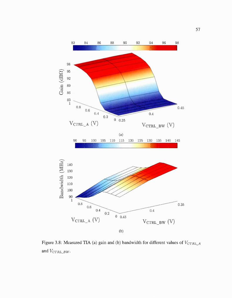
57
82 84 86 88 90 92 94 96 98
98
~
95 c p:)
92 '""()
~ 89 "@ Cj 86
83 1
0.45
VcTRL A (V) 0 0. 35
VcTRL Bw (V)
(a)
90 95 100 105 110 115 120 125 130 135 140 145
~
N ::c: 140
~ 130 ..._____.
...s:::::: 120 ._;..j
'""()
·~ 110 '""()
100 ~ cl5
p:) 90 1
0.35
0.4 0.2
VcTRL A (V) 0 0.45
VcTRL Bw (V)
(b)
Figure 3.8: Measured TIA (a) gain and (b) bandwidth for different values of VcrRL_A
and VcrRL_BW·
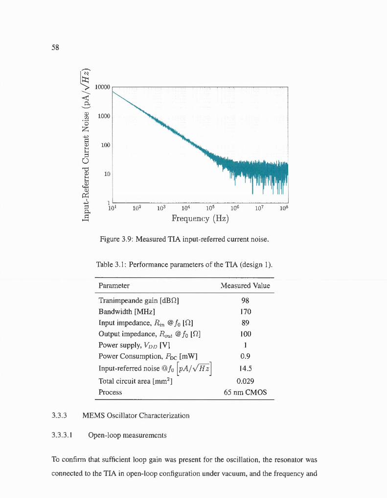
58
,.--__
~ -......__
-< o. .....___, ::J.) (/J -~
0 z -+-" ~ ::1.) '-< '-< ::::l
0 'Ü
::1.) '-< '-<
<2 ::1.)
0:: 1
-+-" ::::l P. ~
..........
10000
1000
100
10
Frequency (Hz)
Figure 3.9 : Measured TIA input-refeiTed current noise.
Table 3.1: Performance parameters of the TIA (design 1 ).
Parameter
Tranimpeande gain [dBD]
Bandwidth [MHz]
Input impedance, ~n @Jo [D]
Output impedance, R aut @Jo [D]
Power supply, V D D [V]
Power Consumption, Poe [mW]
Input-referred noi se @J0 [pA/ JHZ J Total circuit area [mm2 ]
Pro cess
Measured Value
98
170
89
100
(\(\ V . 7
14.5
0.029
65 nm CMOS
3.3.3 MEMS Oscillato r Characteri zati on
3.3.3. 1 Open-loop measurements
To confirm that sufficient loop gain was present for the oscillation, the resonator was
connected to the TIA in open-loop configuration under vacuum, and the frequency and
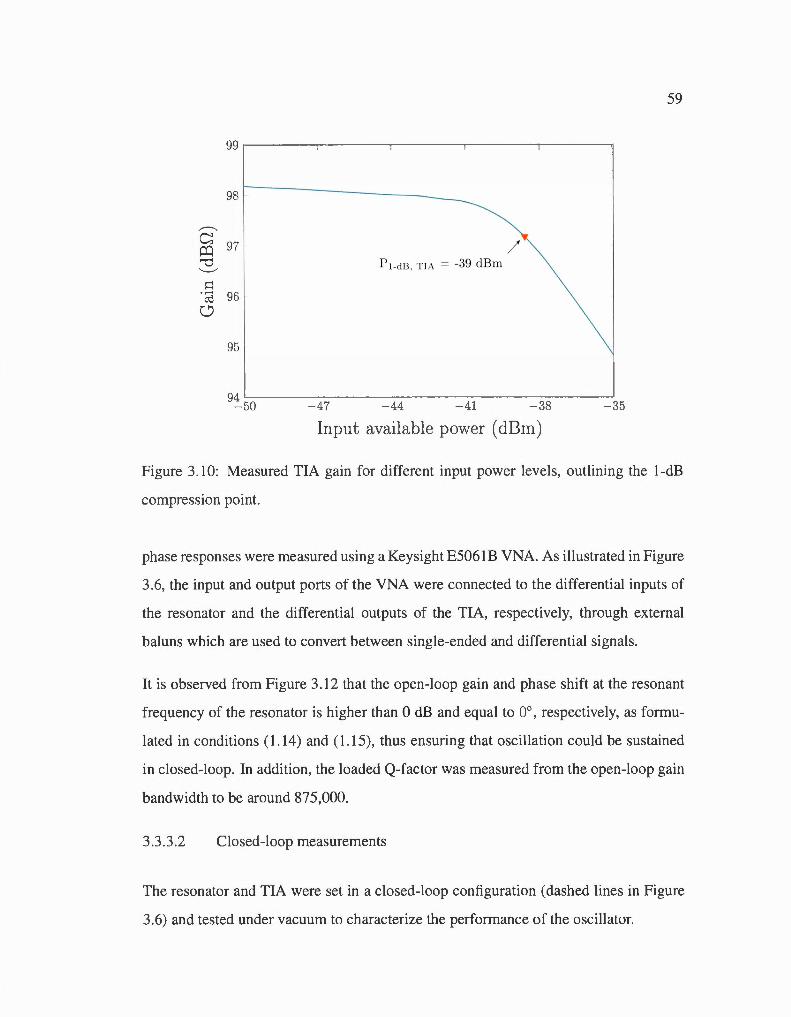
59
99~------------------------------------------.
98
_....---.._
c 97 / o:l '""0 p 1-dB, T I A = -39 dB rn '-.__./
>=1 "@ 96 0
95
94 L-----------------------------------------~ - 50 - 47 - 44 - 41 - 38 - 35
Input available power ( dBm)
Figure 3. 10: Measured TIA gain for different input power levels, outlining the 1-dB
compression point.
phase responses were measured using a Keysight E5061 B VNA. As illustrated in Figure
3.6, the input and output ports of the VNA were connected to the differentiai inputs of
the resonator and the differentiai outputs of the TIA, respectively, through externat
baluns which are used to convert between single-ended and differentiai signais .
It is observed from Figure 3 .1 2 that the open-loop gain and phase shift at the resonant
frequency of the resonator is higher than 0 dB and equal to 0°, respective! y, as formu
lated in conditions ( 1.14) and ( 1.1 5), th us ensuring th at oscillation could be sustained
in closed-loop. ln addition, the loaded Q-factor was measured from the open-loop gain
bandwidth to be around 875,000.
3.3.3.2 Closed-loop measurements
The resonator and TIA were set in a closed-loop configuration (dashed lines in Figure
3.6) and tested under vacuum to characterize the performance of the oscillator.
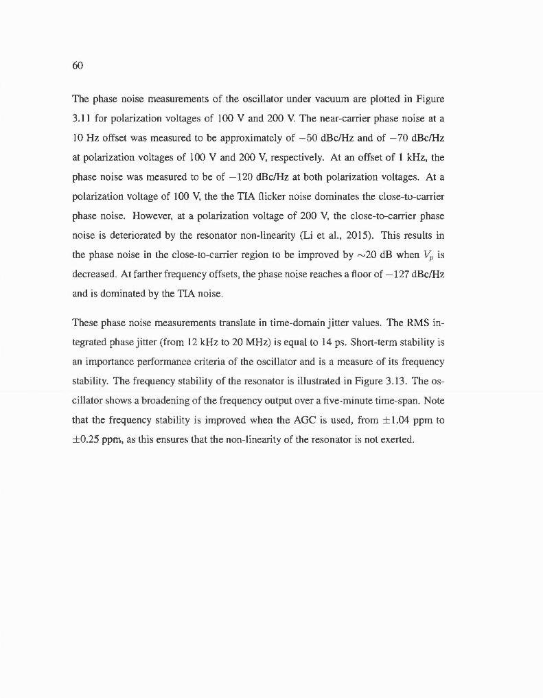
60
The phase noise measurements of the oscillator under vacuum are plotted in Figure
3.11 for polarization voltages of 100 V and 200 V. The near-carrier phase noise at a
10 Hz offset was measured to be approximately of -50 dBc/Hz and of -70 dBc/Hz
at polarization voltages of 100 V and 200 V, respective! y. At an offset of 1 kHz, the
phase noise was measured to be of - 120 dBc/Hz at both polarization voltages. At a
polarization voltage of 100 V, the the TIA flicker noi se dominates the close-ta-carrier
phase noise. However, at a polarization voltage of 200 V, the close-ta-carrier phase
noise is deteriorated by the resonator non-linearity (Li et al., 20 15). This results in
the phase noise in the close-ta-carrier region to be improved by rv20 dB when VP is
decreased. At farther frequency offsets, the phase noise reaches a floor of -127 dBc/Hz
and is dominated by the TIA noise.
These phase noise measurements translate in time-domain jitter values. The RMS in
tegrated phase jitter (from 12kHz to 20 MHz) is equal to 14 ps. Short-term stability is
an importance performance criteria of the oscillator and is a measure of its frequency
stability. The frequency stability of the resonator is illustrated in Figure 3.13. The os
cillator shows a broadening of the frequency output over a five-minute time-span. Note
that the frequency stability is improved when the AGC is used, from ± 1.04 ppm to
± 0.25 ppm, as this ensures that the non-linearity of the resonator is not exerted.
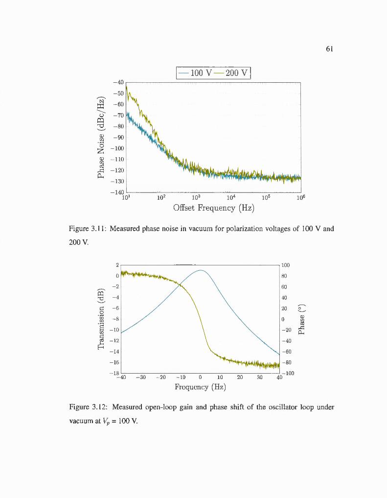
61
I- 100V - 200V I -40
- 50 _.---..
N -60 ::r::
-----u - 70 co '"'0 - 80 ..____..-
Q.) -90 en <3 - 100 z
Q.) - llO en cO
....c: - 120 P-.
- 130
- 140 101 10
Offset Frequency (Hz)
Figure 3.11: Measured phase noi se in vacuum for po1ari zation voltages of 100 V and
200 v.
2 100
0 80
- 2 60 ..-----. j::Q
-4 40 -o ..__.. -6
..-----. ~ 20 0
0 ..__..
[ j) -8 0 Q.)
[/) [/)
·a cO - 10 -20 ....c:
rn o... >::: cO 1-<
- 12 - 40 b
-14 -60
-16 -80
- 18 - 100 - 40 - 30 - 20 - 10 0 10 20 30 40
Frcqucncy (Hz)
Figure 3. 12: Measured open-1oop gain and phase shift of the oscillator 1oop under
vacuum at Vp = 100 V.
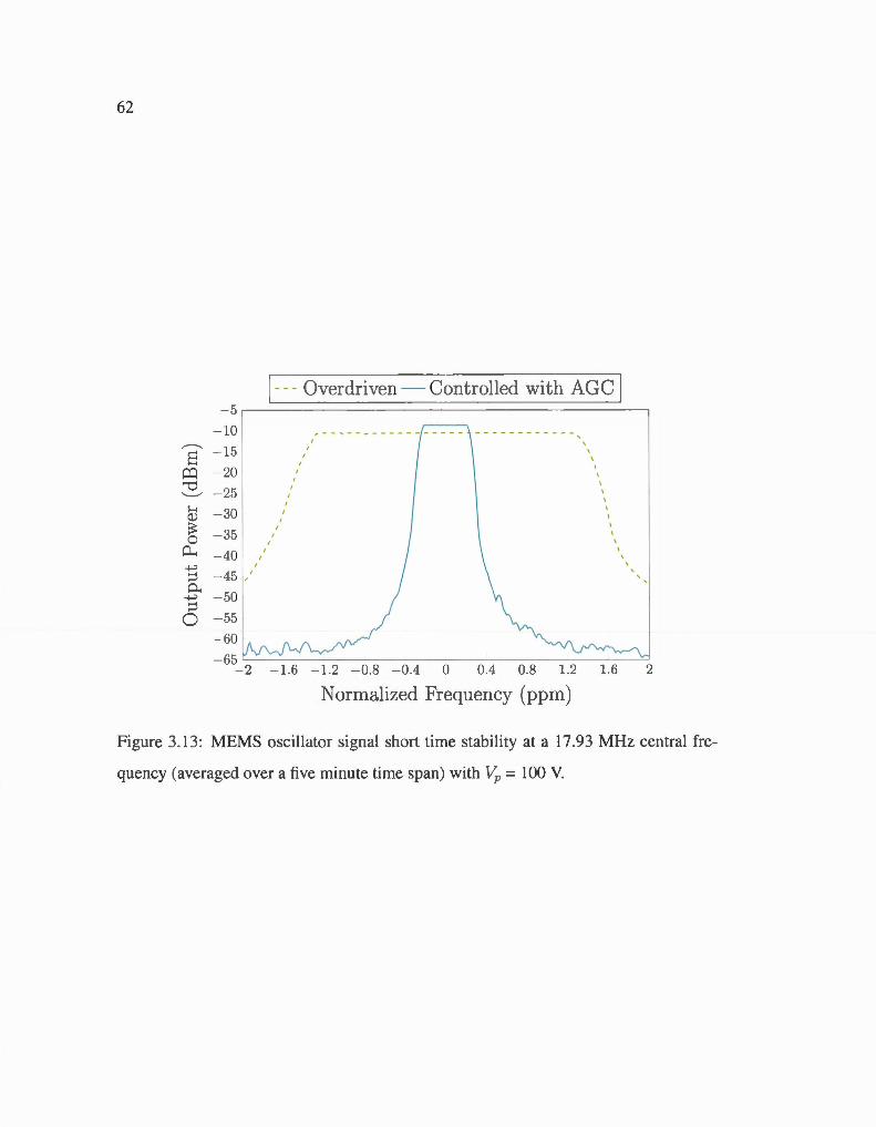
62
1--- Overdriven - Controlled with AGC 1 - 5
- 10 - -----------'
~ ' \
8 - 15 '
\ \
p::) - 20 ' 1 1
'"0 1
1
..._____..- - 25 1
...... Q) - 30 1
;s: - 35 ' 0 '
P-. - 40 ' ' ~ ' ;:::) - 45 /
0.. - 50 ~
;:::)
0 -55
- 60
- 1.2 - 0. - 0.4 0 0.4 0.8 1.2 1.6 2
Normalized Frequency (ppm)
Figure 3.13: MEMS oscillator signal short time stability at a 17.93 MHz central fre
quency (averaged over a five minute ti me span) with Vp = 100 Y.
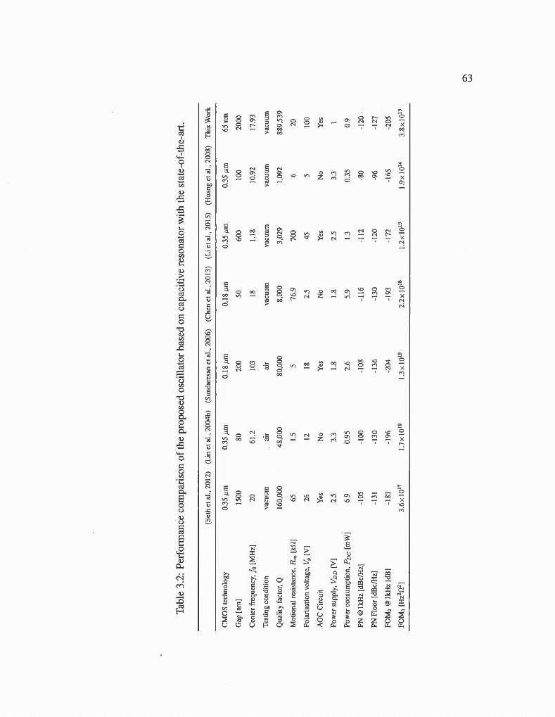
Tab
le 3
.2:
Per
form
ance
com
pari
son
of t
he p
ropo
sed
osci
llat
or b
ased
on
capa
citi
ve r
eson
ator
with
the
sta
te-o
f-th
e-ar
t.
(Set
h et
al.
, 20
12)
(Lin
et a
l., 2
004b
) (S
unda
resa
n et
al.
, 200
6)
(Che
n et
al.
, 201
3)
(Li
et a
l., 2
0 15
) (H
uan
g et
al.,
200
8)
Thi
s W
ork
CM
OS
tec
hnol
ogy
0.35
pm
0.
35 J.
Lffi
0.18
p.m
0
.18/
Lffi
0.
3s1~m
0.3
5 1~m
65 n
m
Gap
[nm
] 15
00
80
200
50
600
100
2000
Cen
ter
freq
uenc
y, J
o [M
HZ!
20
61
.2
103
18
1.18
10
.92
17.9
3
Tes
tin
g co
ndit
ion
vacu
um
air
air
vac
uum
va
cuum
va
cuum
va
cuu
m
Qua
lity
fact
or,
Q
160
,000
48
,000
80
,000
8,
000
3,02
9 1,
092
889
,539
Mot
ion
al r
esis
tanc
e, R
m 1
k!!]
65
1.
5 5
76.9
70
0 6
20
Pola
risa
tio
n vo
ltage
, V,,
1 V J
26
12
18
2.5
45
5
100
AG
C C
ircu
it Y
es
No
Y es
N
o Y
es
No
Y es
Pow
er s
uppl
y, V
vv [
V]
2.5
3.
3 1.
8 1.
8 2.
5 3.
3
Pow
er c
ons
umpt
ion
, Pvc [
mW
] 6.
9 0.
95
2.6
5.9
1.
3 0.
35
0.9
PN @
1 kH
z [d
Bc/
HzJ
-1
05
-lOO
-1
08
-11
6 -1
12
-80
-120
.
PN F
loor
[dB
c/H
zl
-131
-1
30
-136
-1
30
-120
-9
6 -1
27
FO
M2
@1k
Hz
[dB
] -1
83
-196
-2
04
- 193
-1
72
-165
-2
05
FO
M3
[Hz2
rl2
J 3
.6x
l017
1.
7x
l019
1.
3x
1019
2.
2x
1018
1.
2x
l019
1.
9x
1014
3
.8 x
10
19
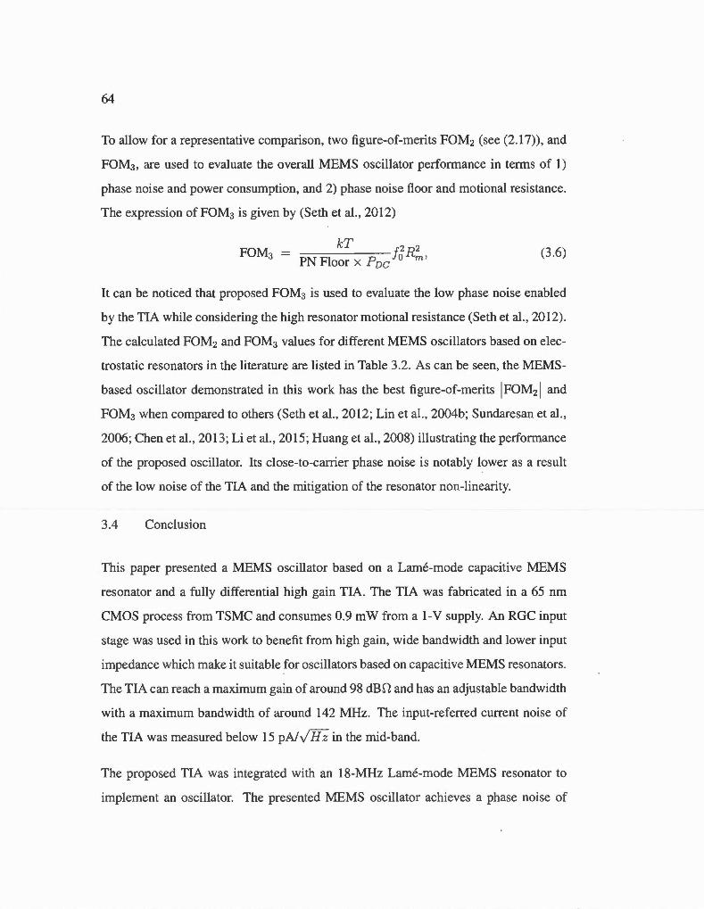
64
To allow for a representative comparison, two figure-of-merits FOM2 (see (2.17)), and
FOM3, are used to evaluate the overall MEMS oscillator performance in terms of 1)
phase noise and power consumption, and 2) phase noise floor and motional resistance.
The expression of FOM3 is given by (Seth et al., 2012)
FOM3 = kT j"z Rz PN Floor x Pvc 0
m > (3.6)
lt can be noticed that proposed FOM3 is used to evaluate the low phase noise enabled
by the TIA while considering the high resonator motional resistance (Seth et al., 2012).
The calculated FOM2 and FOM3 values for different MEMS oscillators based on elec
trostatic resonators in the literature are listed in Table 3.2. As can be seen, the MEMS
based oscillator demonstrated in this work has the best figure-of-merits IFOM2 1 and
FOM3 when compared to others (Seth et al., 2012; Lin et al. , 2004b; Sundaresan et al.,
2006; Chen et al., 2013; Li et al., 2015; Huang et al. , 2008) illustrating the performance
of the proposed oscillator. lts close-to-carrier phase noise is notably lower as a result
of the low noise of the TIA and the mitigation of the resonator non-linearity.
3.4 Conclusion
This paper presented a MEMS oscillator based on a Lamé-mode capacitive MEMS
resonator and a fully differentiai high gain TIA. The TIA was fabricated in a 65 nm
CMOS process from TSMC and consumes 0.9 mW from a 1-V supply. An RGC input
stage was used in this work to benefit from high gain, wide bandwidth and lower input
impedance which make it suitable for oscillators based on capacitive MEMS resonators .
The TIA can reach a maximum gain of around 98 dBD and hasan adjustable bandwidth
with a maximum bandwidth of around 142 MHz. The input-referred current noise of
the TIA was measured below 15 pAJVJiZ in the mid-band.
The proposed TIA was integrated with an 18-MHz Lamé-mode MEMS resonator to
implement an oscillator. The presented MEMS oscillator achieves a phase noise of
65
-120 dBc/Hz, at a 1-kHz offset and the phase noi se floor is of -127 dBc/Hz. The
oscillator exhibits a superior figure-of-merit relative to the state-of-the-art in terms of
power consumption and phase noise.

CONCLUSION
In this thesis, the realization of CMOS transimpedance amplifier capable to interface
with series-resonant MEMS oscillator applications was studied. First, a Verilog-A
madel for a clamped-clamped bearn resonator was presented where electrical and me
chanical non-linear effects were exposed. Moreover a transimpedance amplifier de
signed in 0.13 J.Lm CMOS was implemented with the madel and MEMS-based oscillator
simulation performances were done. The main goal of this work was to design two mi
cromechanical reference oscillators based on bath piezoelectric and capacitive MEMS
resonators. The MEMS resonators presented here were developed in previous works
(Eisayed & Nabki , 2017; Elsayed et al., 20 16). Moreover, two transimpedance ampli
fier designs were studied in details in which frequency and noi se analyses were devel
oped for tradeoff condiseration. The first design was interfaced with the Lamé-mode
capacitive resonator (Elsayed & N abki, 20 17). This design was characterized with
higher gain in arder to compensate resonator's lasses, thereby sustaining oscillation. A
regulated cascade (RGC) topology was used as an input stage to benefit from high gain
with lower input stage and power consumption. The second transimpedance amplifier
was interfaced with bulk-mode di sk piezoelectric resonator (Elsayed et al., 20 16). This
design had a lower gain since the motional resistance of piezoelectric resonators is low.
The input stage of the second design was based on RGC topology mixing with common
source active feedback advantage topology in which lower input-referred current noi se
and larger bandwidth were achieved. The architecture of transimpedance amplifiers
was fully differentiai and was characterized with an adjustable gain and bandwidth sep
arately feature. Finally, the measured performances of MEMS-based oscillators were
demonstrated and compared with state-of-the-art oscillators. Proposed MEMS-based
68
oscillators offered superior figure-of-merit in terms of power consumption and phase
noise.
Future research will be focused on modeling Lamé-mode and disk resonators for further
non-linearity effect consideration. Also MEMS switch will be used in MEMS-based
oscillator to select from multiple resonators interfaced with the TIA in one single chip.
APPENDIX A
CMOS CHIP AND CHARACTERIZATION EVALUATION TEST BOARD
A.l Printed circuit evaluation board
A Printed circuit board (PCB) was des igned in arder to characterize the transi mpedance
amplifiers. The double sided PCB shawn in Figure A.l and Figure A.2 was made
with a standard 0.062 in ("' 1.5 mm) glass-reinforced FR-4 epoxy laminate and the
final dimension was 10 x 15 cm2. The different power supplies are provided from off
chip low dropout (LDO) voltage linear regulators where their input power supplies are
generated through one source path with available option of concocting to an external
DC power supply or 3 x AAA batteries.
A.2 CMOS Transimpedance amplifier chip
A 48-pin QFN socket was used to place available CMOS chip packages for easier use.
The micrograph of CMOS chip die is provided in Figure A.3 where TIAs were fabri
cated using TSMC 65 nm process. The die has 48 pins with dimension of 1.5 x 0.7 mm2
and contains two main different des igns for transimpedance amplifier. Each design was
cloned in such a way for bath designs, every TIA's stage hasan external pin connection.
It is noted that every design has a separate power supply pact . Thus, the design is se
lected through PCB using two slide switchers. Finally, the 48-QFN functional diagram
package is shawn in Figure A.4 and the pact description is illustrated in Table A.l.
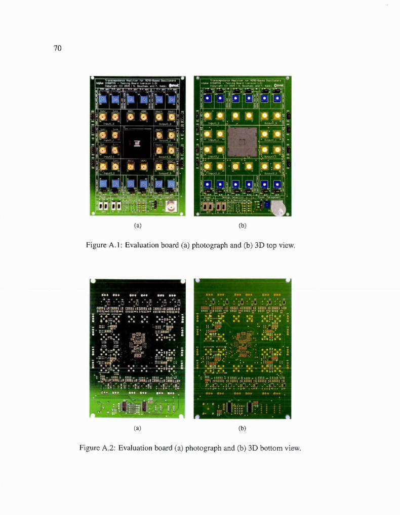
70
Trr.tl~~·""o!LIL••lo•l'll("'l-lntd0tclll•10'1
\Q\111 ~=::.,-(;~·~;-:,•o:-~~;.',0",.,1.,0: lja!Mo .....
(a) (b)
Figure A. l: Evaluation board (a) photograph and (b) 3D top view.
(a) (b)
Figure A.2: Evaluation board (a) photograph and (b) 3D bottom view.
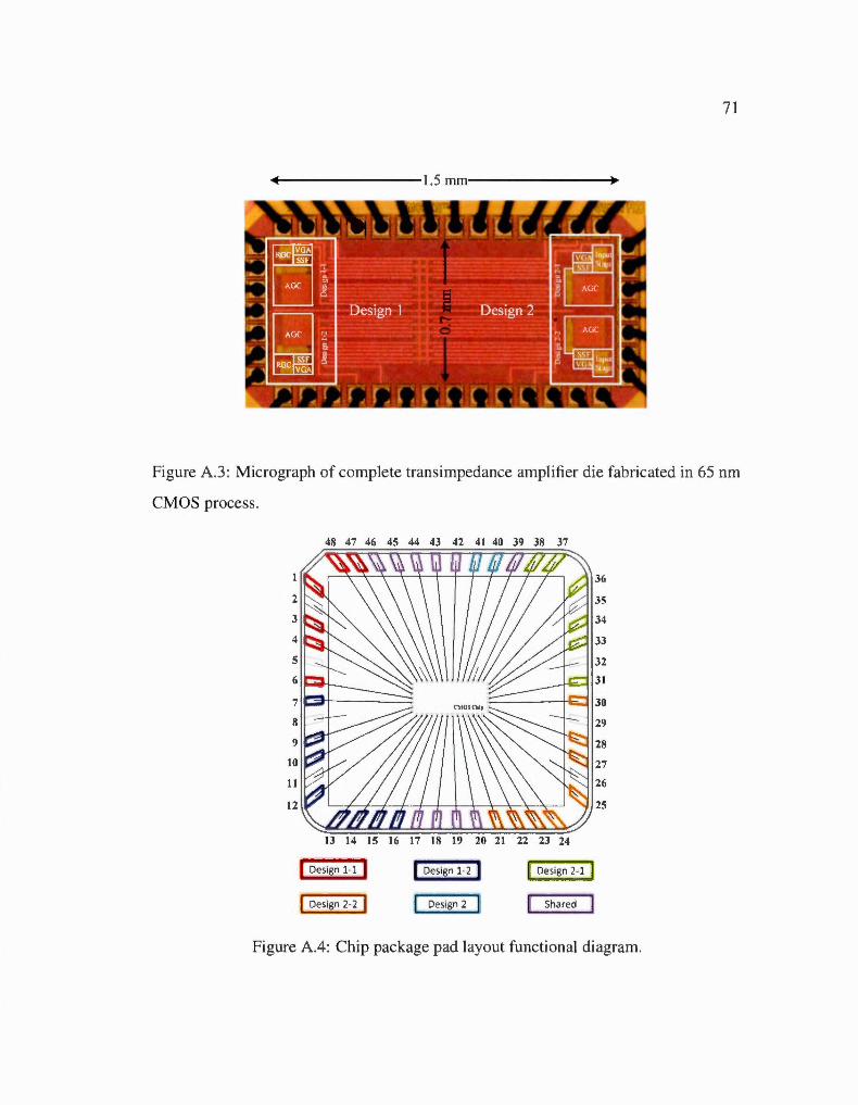
71
..,_--------1.5 mm--------+
Figure A.3: Micrograph of complete transimpedance ampli fier die fabricated in 65 nm
CMOS process.
2
J
4
5
6 ,__...,.__
7 t::;ilH------=
8
9
10
I l
12
IJ 14
1 Design 1-1 1
1 Design 2-2 1
15 16 17 18 19 20
1 Design 1-2 1
1 Design 2
1
J6
JS
J4
JJ
32
JI
-----1--k:;-l JO
21 22 2J 24
1 Design 2-1 1
1 Shared
1
29
28
27
26
25
Figure A.4: Chip package pad layout functional diagram.
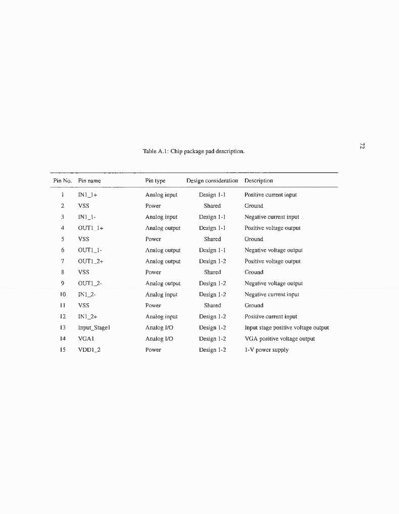
Table A.l: Chip package pad descripti on.
Pin No. Pinname Pin type Design consideration Description
INI - 1+ Analog input Design 1-1 Positi ve CUITent input
2 vss Power Shared Grou nd
3 INI - 1- Analog input Design 1-1 Negati ve current input
4 OUT ! - 1+ Analog output Design 1- 1 Positive voltage output
5 vss Power Shared Grou nd
6 OUT ! 1- Analog output Design 1- 1 Negative voltage output
7 OUT ! - 2+ Analog output Design 1-2 Positive voltage output
8 vss Power Shared Grou nd
9 OUT ! 2- Analog output Design 1-2 Negati ve voltage output
JO IN I - 2- Analog input Design 1-2 Negati ve current input
Il vss Power Shared Ground
12 INJ - 2+ Analog input Design 1-2 Positive current input
13 lnput_Stage l Analog 110 Design 1-2 Input stage posi ti ve voltage output
14 VGAI Analog l/0 Design 1-2 VGA positive voltage output
15 VDDI 2 Power Design 1-2 1-V power supply
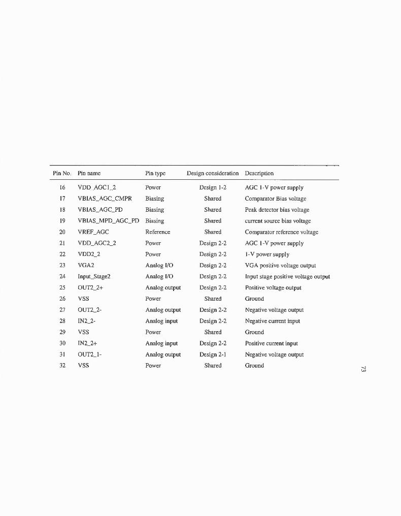
Pin No. Pin name Pin type Design considerati on Description
16 VDD_AGCl 2 Power Design 1-2 AGC 1-V power supply
17 VBlAS_AGC_CMPR Biasing Shared Comparator Bias vo ltage
18 VBlAS_AGC_PD Biasing Shared Peak detector bias voltage
19 VBlAS_MPD_AGC_PD Biasing Shared current source bias voltage
20 VREF_AGC Reference Shared Compara tor reference voltage
2 1 VDD_AGC2_2 Power Design 2-2 AGC 1-V power supply
22 VDD2_2 Power Design 2-2 1-V power supply
23 VGA2 Analog 1/0 Design 2-2 VGA positi ve voltage output
24 Input_Stage2 Analog 1/0 Design 2-2 Input stage positive voltage output
25 OUT2_2+ Analog output Design 2-2 Positive voltage output
26 vss Power Shared Ground
27 OUT2_2- Analog output Design 2-2 Negative voltage output
28 IN2_2- Analog input Design 2-2 Negative current input
29 vss Power Shared Ground
30 IN2_2+ Analog input Design 2-2 Positive current input
31 OUT2 - 1- Analog output Design 2- 1 Negative voltage output
32 vss Power Shared Ground -.) w
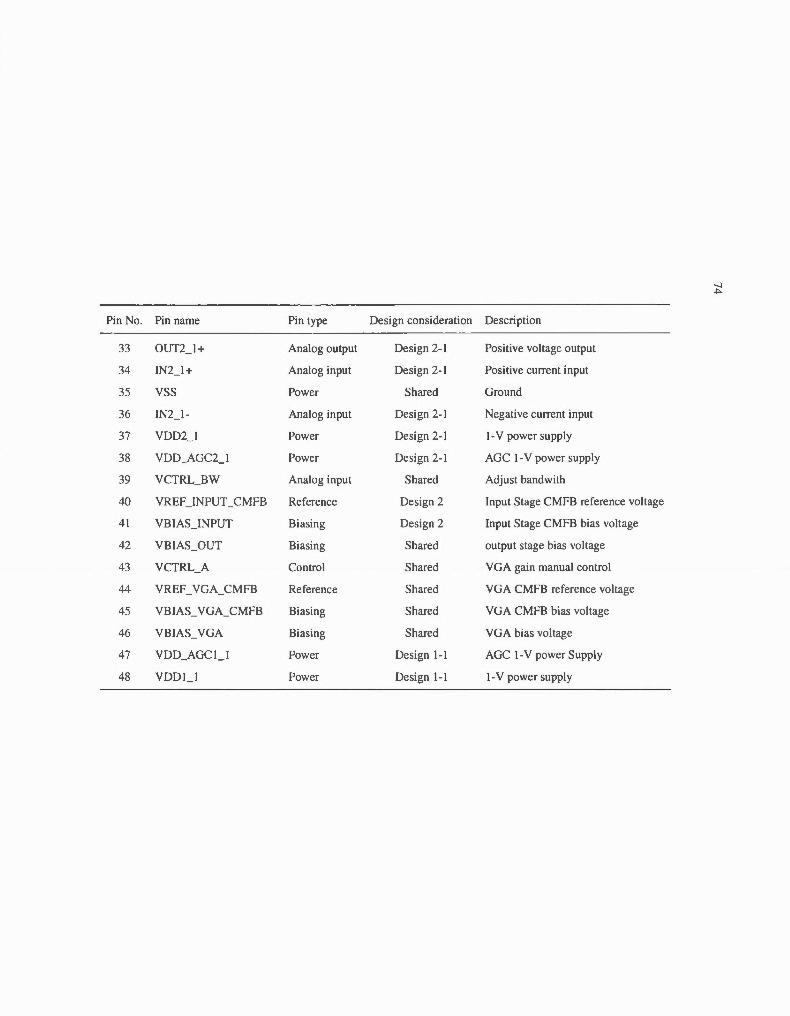
-.]
""" Pin No. Pin name Pin type Design consideration Description
33 OUT2_ 1+ Analog output Design 2- 1 Posit ive voltage output
34 IN2_ 1+ Analog input Design 2- 1 Positive current input
35 vss Power Shared Grou nd
36 IN2_1- Analog input Design 2- 1 Negative current input
37 VDD2_ 1 Power Design 2- 1 1-V power supply
38 VDD_AGC2 - Power Design 2- 1 AGC 1-Y power supply
39 YCTRL_BW Anal og input Shared Adjust bandwith
40 VREF _INPUT _C MFB Reference Design 2 Input Stage CMFB reference voltage
4 1 VBIAS_INPUT Biasing Design 2 Input Stage CMFB bias voltage
42 VBIAS_OUT Bias ing Shared output stage bias voltage
43 VCTRL_A Control Shared YGA gain manua l control
44 VR EF _ VGA_CMFB Reference Shared YGA CMFB reference vo ltage
45 V BIAS_ VGA_CMFB Biasing Shared YGA CMFB bias voltage
46 VBIAS_YGA Biasing Shared VGA bias voltage
47 VDD_AGCI - 1 Power Design 1-1 AGC 1-Y power Supply
48 YOD! - 1 Power Design 1-1 1-V power suppl y
BIDLIOGRAPHY
Agarwal, M., Park, K. K., Kim, B., Hopcroft, M. A. , Chandorkar, S. A. , Candler, R. N., Jha, C. M., Melamud, R. , Kenny, T. W. & Murmann, B. (2006). Amplitude noise induced phase noi se in electrostatic MEMS resonators. In Solid State Sensor, Actuator, and Microsystems Workshop.
Agrawal, 0 ., Woodhouse, J. & Seshia, A. (2013). Modeling nonlinearities in MEMS oscillators. IEEE Trans. Ultrasonics, Ferroelectrics and Frequency Control, 60(8) , 1646- 1659.
Baghelani , M. , Ghavifekr, H. B. & Ebrahimi , A. (20 13). MEMS based oscillator for UHF applications with automatic amplitude control. Microelectronics Journal, 44(4) , 292 - 300.
Baltes, H., Brand, 0 ., Hierlemann, A., Lange, O. & Hagleitner, C . (2002). Cmos mems - present and future . In Technical Digest. MEMS 2002 IEEE International Conference. F(fteenth IEEE International Conference on Micro Electro Mechanical Systems, pp. 459-466.
Bouchami, A. & Nabki, F. (2014) . Non-linear modeling of MEMS-based oscillators using an analog hardware description language. In 20I4 IEEE 12th International New Circuits and Systems Conference (NEWCAS).
Burden, R. & Faires, J. (20 11). Numerical Analysis. Brooks/Cole, Cengage Learning.
Carusone, T. C., Johns, O. & Martin, K. (20 Il). Analog Integrated Circuit Design. John Wiley & Sons, Inc.
Chen, T.-T., Huang, J.-C. , Peng, Y.-C., Chu, C.-H., Lin, C.-H., Cheng, C.-W., Li , C.S. & Li , S.-S . (20 13). A 17.6-MHz 2.5V ultra-low polarization voltage MEMS oscillator using an innovative high gain-bandwidth fully differentiai trans-impedance voltage amplifier. In 20!3 IEEE 26th International Conference on Micro Electro Mechanical Systems (MEMS).
Clark, J. , Hsu, W.-T., Abdelmoneum, M. & Nguyen, C.-C. (2005). High-Q UHF micromechanical radial-contour mode di sk resonators. Journal of Microelectromechanical Systems, I4(6) , 1298- 1310.
76
Elsayed, M. , Nabki, F. & El-Gama!, M. (20 Il). A 2000° /s dynamic range bulk mode dodecagon gyro for a commercial SOI technology. In 2011 18th IEEE International Conference on Electronics, Circuits, and Systems.
Elsayed, M. Y., Cicek, P. V., Nabki , F. & El-Gama!, M . N. (2016). Bulk Mode Disk Resonator With Transverse Piezoelectric Actuation and Electrostatic Tuning. Journal of Microelectromechanical Systems, 25(2), 252-261.
Elsayed, M . Y. & Nabki, F. (20 17). 18-MHz Silicon Lamé Mode Resonators With Corner and Central Anchor Architectures in a Duai-Wafer SOI Technology. Journal ofMicroelectromechanical Systems, 26(1), 67- 74.
Elsayed, M. Y., Nabki, F. & El-Gama!, M . N. (2013a). A combined comb 1 bulk mode gyroscope structure for enhanced sensitivity. In 2013 IEEE 26th International Conference on Micro Electro Mechanical Systems (MEMS).
Elsayed, M. Y., Nabki, F. & El-Gama!, M. N. (20 13b). A novel comb architecture for enhancing the sensitivity of bulk mode gyroscopes. Sensors , 13( 12), 16641-16656.
Filler, R. ( 1985). The amplitude-frequency effect in SC-eut resonator . In 39th Annual Symposium on Frequency Control, pp. 311 - 316.
Gong, S. & Piazza, G. (2013). Design and Analysis of Lithium-Niobate-Based High Electromechanical Coupling RF-MEMS Resonators for Wideband Filtering. IEEE Transactions on Microwave The ory and Techniques, 61 ( 1 ), 403--414.
Gray, P. R. , Hurst, P.J . & Lewis, S. H. (2009). Analysis and Design of Analog lntegrated Circuits . John Wiley & Sons, Inc.
Hajimiri , A. & Lee, T. ( 1998). A General Theory of Phase Noise in Electrical Oscillators . IEEE Journal of Solid-State Circuits, 33(2), 179- 194.
He, F., Ribas, R., Lahuec, C. & Jézéquel , M. (2009). Discuss ion on the general oscillation startup condition and the Barkhausen criterion. Analog Integrated Circuits and Signal Processing, 59(2), 215- 221.
Huang, W.-L., Ren , Z., Lin, Y.-W., Chen, H.-Y., Lahann, J. & Nguyen, C. T. C. (2008). Fully monolithic CMOS nickel micromechanical resonator osci ll ator. In 2008 IEEE 21st International Conference on Micro Electro Mechanical Systems, pp. 10- 13 .
Hung, L.-W. & Nguyen, C. T.-C. (2011). Capacitive-piezoelectric AIN resonators with Q> 12,000. In 2011 IEEE 24th International Conference on Micro Elecrro Mechanical Systems.
Kaajakari , V., Mattila, T., Oja, A. & Seppa, H. (2004). Nonlinear Limits for SingleCrystal Silicon Microresonators. Journal of Microelectromechanical Systems, 13(5) ,
77
715- 724.
Konishi, T., Machida, K., Maruyama, S., Mita, M. , Masu, K. & Toshiyoshi, H. (2013). A Single-Platform Simulation and Design Technique for CMOS-MEMS Based on a Circuit Simulator With Hardware Description Language. JMEMS, 22(3), 755-767.
Kopa, A. & Apse1, A. B. (2008). 124dB·Hz213 Dynamic range transimpedance amplifier for electronic-photonic channelizer. In 2008 IEEE International Symposium on Circuits and Systems.
Lavasani, H. M. , Abdolvand, R. & Ayazi, F. (20 15). Single-resonator dual-frequency AIN-on-Si MEMS oscillators. IEEE Transactions on Ultrasonics, Ferroelectrics, and Frequency Control, 62(5), 802-813.
Lavasani, H. M. , Pan, W., Hanington, B. , Abdolvand, R. & Ayazi, F. (20 11 ). A 76 dBD 1.7 GHz 0.18 p,m CMOS Tunable TIA Using Broadband Cunent Pre-Amplifier for High Frequency Lateral MEMS Oscillators. IEEE Journal of Solid-State Circuits, 46( 1 ), 224- 235 0
Lavasani, H. M., Pan, W. , Harrington, B. P., Abdolvand, R. & Ayazi , F. (20 12). Electronic Temperature Compensation of Lateral Bulk Acoustic Resonator Reference Osci llators Using Enhanced Series Tuning Technique. IEEE Journal of Solid-State Circuits, 47(6), 1381-1393.
Lee, H., Ward, P. , Duwel , A., Salvia, J., Qu, Y., Melamud, R., Chandorkar, S., Hopcroft, M. , Kim, B. & Kenny, T. (2011 ). Verification of the phase-noise model for MEMS oscillators operating in the nonlinear regime. In Solid-State Sensors, Actuators and Microsystems Conference (TRANSDUCERS), 2011 16th International, pp. 510-513.
Lee, S. & Nguyen, C.-C. (2003). Influence of automatic leve! control on micromechanical resonator oscillator phase noise. In IEEE International Frequency Control Sympposium and PDA Exhibition Joint/y with the 17th European Frequency and Time Forum, 2003. Proceedings of the 2003, pp. 341-349.
Li , M.-H., Chen, C.-Y., Li, C.-S., Chin, C.-H. & Li, S.-S. (20 15). A Monolithic CMOSMEMS Oscillator Based on an Ultra-Low-Power Ovenized Micromechanical Resonator. Journal of Microelectromechanical Systems, 24(2), 360-372.
Li , M.-H., Li , C.-S., Hou, L.-J., Liu, Y.-C. & Li, S.-S. (2012) . A 1.57mW 99dBD CMOS transimpedance amplifier for VHF micromechanical reference oscillators . In 2012 IEEE International Symposium on Circuits and Systems.
Lin, Y. -W., Lee, S. , Li, S .-S ., Xie, Y., Ren, Z. & Nguyen, C.-C. (2004a). Series-resonant VHF micromechanical resonator reference oscillators. IEEE Journal of Solid-State
78
Circuits, 39(12), 2477- 2491.
Lin, Y.-W., Lee, S., Li, S.-S., Xie, Y., Ren, Z. & Nguyen, C. T. C. (2004b). 60-MHz wine-glass micromechanical-disk reference oscillator. In 2004 IEEE International Solid-State Circuits Conference (IEEE Cat. No.04CH375I9), pp. 322- 530 Vol.l.
Mestrom, R. , Fey, R. , van Beek, J. , Phan, K. & Nijmeijer, H. (2008). Modelling the dynamics of a MEMS resonator: Simulations and experiments. Sensors and Actuators A: Physical, I42( 1 ), 306 - 315 . Special Issue: Eurosensors XX The 20th European conference on Solid-State Transducers Eurosensors 2006 Eurosensors 20th Edition.
Mestrom, R. M. C. , Fey, R. H. B. & Nijmeijer, H. (2009). Phase Feedback for Nonlinear MEM Resonators in Oscillator Circuits . IEEE/ASME Trans. Mechatronics, Transactions, I4(4 ), 423-433.
Nabki , F. (20 1 0). Silicon Carbide Micro-Electromechanical Resonators f or Highly Integrated Frequency Synthesizers . (PhD thesi ). McGill University.
Nabki , F. , Allidina, K., Ahmad, F. , Cicek, P.-V. & El-Gama], M. N. (2009). A Highly Integrated 1.8 GHz Frequency Synthesizer Based on a MEMS Resonator. IEEE Journal of Solid-State Circuits, 44(8) , 2154- 2168.
Nabki , F. & El-Gama!, M . N. (2008). A high gain-bandwidth product transimpedance amplifier for MEMS-based oscillators. In ESSCIRC 2008 - 34th European SolidState Circuits Conference .
Ogawa, K. ( 1981 ). Noise Caused by GaAs MESFETs in Optical Receivers. Bell System Technical Journal, 60(6), 923- 928.
Park , S. & Yoo, H.-J. (2004). 1.25-Gb/s Regulated Cascode CMOS Tran impedance Amplifier for Gigabit Ethernet Applications. IEEE Journal of Solid-State Circuits , 39( 1), 112- 121.
Park, S. M. & Toumazou, C. (2000). A packaged low-noise high-speed regulated cascode transimpedance amplifier using a 0.6mum N-well CMOS technology. In Proceedings of the 26th European Solid-State Circuits Conference, pp. 431-434.
Pettine, J ., Petrescu, V. , Karabacak, D. M., Vandecasteele, M ., Crego-Calama, M. & Hoof, C. V. (20 12). Power-Efficient Oscillator-Based Readout Circuit for Multichannel Resonant Volatile Sensors. IEEE Transactions on Biomedical Circuits and Systems, 6(6), 542-55 1.
Razav i, B . (2000). A 622 Mb/s 4 . 5pA/~ CMOS transimpedance amplifier [for optical receiver front-end] . In 2000 IEEE International Solid-State Circuits Conference., pp. 162- 163.
79
Rebeiz, G. (2004). RF MEMS: Theory, Design, and Technology. Wiley.
Ruffieux, D., Krummenacher, F., Pezous, A. & Spinola-Durante, G. (2010). Silicon Resonator Based 3.2 J-LW Real Time Clock With ±10 ppm Frequency Accuracy. IEEE Journal of Solid-State Circuits, 45( 1 ), 224-234.
Sackinger, E . & Guggenbuhl, W. ( 1990). A High-Swing, High-Impedance MOS Cascode Circuit. IEEE Journal of Solid-State Circuits, 25( 1 ), 289-298.
Salvia, J., Lajevardi, P., Hekmat, M. & Murmann, B. (2009). A 56MD CMOS TIA for MEMS applications. In 2009 IEEE Custom Integrated Circuits Conference.
Schneider, R. A. & Nguyen, C. T.-C. (2014). On/off switchable high-Q capacitivepiezoelectric AIN resonators. In 20I4 IEEE 27th International Conference on Micro Electro Mechanical Systems (MEMS).
Senturia, S. (2000). Microsystem Design. Springer.
Seth, S., Wang, S., Kenny, T. & Murmann, B. (20 12). A -131-dBc/Hz, 20-MHz MEMS oscillator with a 6.9-mW, 69-kD., gain-tunable CMOS TIA. In 20I2 Proceedings of the ESSCIRC ( ESSCIRC).
Shaeffer, D. & Lee, T. ( 1997). A 1.5-V, 1.5-GHz CMOS low noi se amplifier. IEEE Journal ofSolid-State Circuits, 32(5), 745- 759.
Shao, L. C. , Palaniapan, M. & Tan, W. W. (2008). The nonlinearity cancellation phenomenon in micromechanical resonators. Journal of Micromechanics and Microengineering, 18(6), 065014.
SiTime Corporation (20 17) . SiTime Enables Industrial loT Applications with Smallest, Lowest-Power, Precision MEMS Reference Clocks. [Online; accessed July 22, 2017]. Retrieved from https : 1 /www . sitime . corn/news/ press-releases/
Sundaresan, K., Ho, G., Pourkamali, S. & Ayazi, F. (2006). A Low Phase Noise 1 OOMHz Silicon BAW Reference Oscillator. In IEEE Custom Integrated Circuits Conference 2006.
van Beek, J. T. M. & Puers, R. (20 12). A review of MEMS oscillators for frequency reference and timing applications. J. of Micromech. and Microeng., 22( 1 ), 013001.
Van Caekenberghe, K. (2012). Modeling RF MEMS Deviees. IEEE Microwave Magazine, 13( 1 ), 83- 11 O.
Weiner, J. , Leven, A. , Houtsma, V., Baeyens, Y., Chen, Y.-K., Paschke, P. , Yang, Y., Frackoviak, J. , Sung, W.-J. , Tate, A. , Reyes, R ., Kopf, R. & Weimann, N. (2003). SiGe differentiai transimpedance amplifier with 50-GHz bandwidth. IEEE Journal
80
of Solid-State Circuits, 38(9), 1512-1517.
Wenbo, W., Luhong, M., Xindong, X., Shilin , Z. & Sheng, X. (2013). A differentia! automatic gain control circuit with two-stage -10 to 50 dB tuning range V GAs. Journal of Semiconductors, 34(2), 025008.
Wu, Z. & Rais-Zadeh, M . (20 15). A Temperature-Stable Piezoelectric MEMS Oscillator Using a CMOS PLL Circuit for Temperature Sensing and Oven Control. Journal of Microelectromechanical Systems, 24(6), 1747- 1758.
Xie, Y., Li , S.-S., Lin , Y.-W., Ren, Z . & Nguyen , C.-C. (2008). 1.52-GHz micromechanical extensional wine-glass mode ring resonators. IEEE Transactions on Ultrasanies, Ferroelectrics and Frequency Control, 55(4) , 890-907.
Yuan, F. & Sun, B. (2002). A comparative study of low-voltage CMOS CUITent-mode circuits for optical communications. In The 2002 45th Midwest Symposium on Circuits and Systems, 2002. MWSCAS-2002, pp. I- 3 15- 19 vol.!.
Zhu, H. & Lee, J. E.-Y. (20 12) . Reversed Nonlinear Osci ll at ions in Lamé-Mode SingleCrystal-Silicon Microresonators. IEEE Electron Deviee Letters, 33( 1 0), 1492- 1494.
Zhu, H. & Lee, J . E.-Y. (20 14). Orientati on dependence of nonlinearity and TCf in highQ shear-modes of silicon MEMS resonators. In 2014 IEEE International Frequency Control Symposium (FCS) .
Zhu, H ., Tu , C. & Lee, J. E.-Y. (20 12). Material nonlinearity limits on a Lamémode single crystal bulk resonator. In 2012 7th IEEE International Conference on Nana/Micro Engineered and Molecular Systems (NEMS).
Zuo, C. , Spiegel, J. V. D. & Piazza, G. (20 10). 1.05-G Hz CMOS osc ill ator based on lateral- field-excited piezoelectric AIN contour- mode MEMS resonators. IEEE Transactions on Ultrasonics, Ferroelectrics and Frequency Control, 57( 1 ), 82-87.