Embed Size (px)
Citation preview

8/20/2019 nanoLOC NA5TR1 UserGuide
http://slidepdf.com/reader/full/nanoloc-na5tr1-userguide 1/325
nanoLOC TRX
Transceiver (NA5TR1)
User Guide
Version 2.00NA-06-0230-0385-2.00
This document contains information on a pre-engineering chip.
Specifications and information herein are subject to change with-
out notice.

8/20/2019 nanoLOC NA5TR1 UserGuide
http://slidepdf.com/reader/full/nanoloc-na5tr1-userguide 2/325
Document Information
nanoLOC TRX Transceiver (NA5TR1) User Guide
Page ii NA-06-0230-0385-2.00 © 2007 Nanotron Technologies GmbH.
Document Information
Document Title: nanoLOC TRX Transceiver (NA5TR1) User Guide
Document Version: 2.00
Published (yyyy-mm-dd): 2008-06-06
Current Printing: 2008-6-6, 12:46 pm
Document ID: NA-06-0230-0385-2.00
Document Status: Released
Disclaimer
Nanotron Technologies GmbH believes the information contained herein is correct and accurate at the time of release. NanotronTechnologies GmbH reserves the right to make changes without further notice to the product to improve reliability, function or design. Nanotron Technologies GmbH does not assume any liability or responsibility arising out of this product, as well as anyapplication or circuits described herein, neither does it convey any license under its patent rights.
As far as possible, significant changes to product specifications and functionality will be provided in product specific Erratasheets, or in new versions of this document. Customers are encouraged to check the Nanotron website for the most recentupdates on products.
Trademarks
nanoNET© is a registered trademark of Nanotron Technologies GmbH. All other trademarks, registered trademarks, and productnames are the sole property of their respective owners.
This document and the information contained herein is the subject of copyright and intellectual property rights under internationalconvention. All rights reserved. No part of this document may be reproduced, stored in a retrieval system, or transmitted in anyform by any means, electronic, mechanical or optical, in whole or in part, without the prior written permission of NanotronTechnologies GmbH.
Copyright © 2008 Nanotron Technologies GmbH .
Life Support Policy
These products are not designed for use in life support appli-ances, devices, or systems where malfunction of these prod-ucts can reasonably be expected to result in personal injury.Nanotron Technologies GmbH customers using or sellingthese products for use in such applications do so at their ownrisk and agree to fully indemnify Nanotron TechnologiesGmbH for any damages resulting from such improper use or sale.
Electromagnetic Interference / Compatibility
Nearly every electronic device is susceptible to electromag-netic interference (EMI) if inadequately shielded, designed, or otherwise configured for electromagnetic compatibility.
To avoid electromagnetic interference and/or compatibilityconflicts, do not use this device in any facility where posted
notices instruct you to do so. In aircraft, use of any radio fre-quency devices must be in accordance with applicable regula-tions. Hospitals or health care facilities may be usingequipment that is sensitive to external RF energy.
With medical devices, maintain a minimum separation of 15cm (6 inches) between pacemakers and wireless devices andsome wireless radios may interfere with some hearing aids. If other personal medical devices are being used in the vicinityof wireless devices, ensure that the device has been ade-quately shielded from RF energy. In a domestic environmentthis product may cause radio interference in which case theuser may be required to take adequate measures.
CAUTION! Electrostatic Sensitive Device. Pre-caution should be used when handling thedevice in order to prevent permanent damage.
FCC User Information
Statement according to FCC part 15.19:
This device complies with Part 15 of the FCC Rules. Opera-tion is subject to the following two conditions: (1) this devicemay not cause harmful interference, and (2) this device mustaccept any interference received, including interference thatmay cause undesired operation.
Statement according to FCC part 15.21:
Modifications not expressly approved by this company couldvoid the user's authority to operate the equipment.
RF exposure mobil:
The internal / external antennas used for this mobile transmit-ter must provide a separation distance of at least 20 cm fromall persons and must not be co-located or operating in con-
junction with any other antenna or transmitter.”
Statement according to FCC part 15.105:
This equipment has been tested and found to comply with the
limits for a Class A and Class B digital device, pursuant to Part15 of the FCC Rules. These limits are designed to provide
reasonable protection against harmful interference in a resi-dential installation and against harmful interference when theequipment is operated in a commercial environment.
This equipment generates, uses, and can radiate radio fre-quency energy and, if not installed and used in accordancewith the instructions as provided in the user manual, maycause harmful interference to radio communications. How-ever, there is no guarantee that interference will not occur in aparticular installation. Operation of this equipment in a resi-dential area is likely to cause harmful interference in whichcase the user will be required to correct the interference at hisor her own expense.
If this equipment does cause harmful interference to radio or television reception, which can be determined by turning theequipment off and on, the user is encouraged to try to correctthe interference by one or more of the following measures:• Reorient or relocate the receiving antenna.• Increase the separation between the equipment and
receiver.• Connect the equipment into an outlet on a circuit different
from that to connected.
• Consult the dealer or an experienced technician for help.

8/20/2019 nanoLOC NA5TR1 UserGuide
http://slidepdf.com/reader/full/nanoloc-na5tr1-userguide 3/325
Contents Overview
nanoLOC TRX Transceiver (NA5TR1) User Guide
© 2008 Nanotron Technologies GmbH. NA-06-0230-0385-2.00 Page iii
Contents Overview
Contents Overview . . . . . . . . . . . . . . . . . . . . . . . . . . . . . . . . . . . . . . . . . . . . . . . . . . . . . . . . . . . . . . . . . . .iii
Table of Contents . . . . . . . . . . . . . . . . . . . . . . . . . . . . . . . . . . . . . . . . . . . . . . . . . . . . . . . . . . . . . . . . . . . . v
List of Tables . . . . . . . . . . . . . . . . . . . . . . . . . . . . . . . . . . . . . . . . . . . . . . . . . . . . . . . . . . . . . . . . . . . . . . .xiii
List of Figures . . . . . . . . . . . . . . . . . . . . . . . . . . . . . . . . . . . . . . . . . . . . . . . . . . . . . . . . . . . . . . . . . . . . . . xv
1 How To Use This User Guide. . . . . . . . . . . . . . . . . . . . . . . . . . . . . . . . . . . . . . . . . . . . . . . . . . . . . . . 1
Section One: nanoLOC Chip Programming Guide
2 Key Features . . . . . . . . . . . . . . . . . . . . . . . . . . . . . . . . . . . . . . . . . . . . . . . . . . . . . . . . . . . . . . . . . . . . 7
3 nanoLOC Architecture . . . . . . . . . . . . . . . . . . . . . . . . . . . . . . . . . . . . . . . . . . . . . . . . . . . . . . . . . . . . 9
4 Digital and Analog IO Pins. . . . . . . . . . . . . . . . . . . . . . . . . . . . . . . . . . . . . . . . . . . . . . . . . . . . . . . . 11
5 nanoLOC Clocking Structure. . . . . . . . . . . . . . . . . . . . . . . . . . . . . . . . . . . . . . . . . . . . . . . . . . . . . . 15
6 Power Management . . . . . . . . . . . . . . . . . . . . . . . . . . . . . . . . . . . . . . . . . . . . . . . . . . . . . . . . . . . . . 23
7 nanoLOC Programming Interface (SPI) . . . . . . . . . . . . . . . . . . . . . . . . . . . . . . . . . . . . . . . . . . . . . 298 nanoLOC Memory Map. . . . . . . . . . . . . . . . . . . . . . . . . . . . . . . . . . . . . . . . . . . . . . . . . . . . . . . . . . . 39
9 Chirp Sequencer (CSQ) . . . . . . . . . . . . . . . . . . . . . . . . . . . . . . . . . . . . . . . . . . . . . . . . . . . . . . . . . . 45
10 nanoLOC Packet and MACFrames . . . . . . . . . . . . . . . . . . . . . . . . . . . . . . . . . . . . . . . . . . . . . . . . 49
11 Frame Control Scheme. . . . . . . . . . . . . . . . . . . . . . . . . . . . . . . . . . . . . . . . . . . . . . . . . . . . . . . . . . 57
12 MACFrame Configuration (Auto/Transparent) . . . . . . . . . . . . . . . . . . . . . . . . . . . . . . . . . . . . . . . 59
13 Baseband RAM Configuration. . . . . . . . . . . . . . . . . . . . . . . . . . . . . . . . . . . . . . . . . . . . . . . . . . . . 61
14 Buffer Configuration (Simplex/Duplex). . . . . . . . . . . . . . . . . . . . . . . . . . . . . . . . . . . . . . . . . . . . . 67
15 Buffer Swapping Between TX and RX Buffers. . . . . . . . . . . . . . . . . . . . . . . . . . . . . . . . . . . . . . . 69
16 Buffer Control Timing. . . . . . . . . . . . . . . . . . . . . . . . . . . . . . . . . . . . . . . . . . . . . . . . . . . . . . . . . . . 71
17 Buffer Access Synchronization. . . . . . . . . . . . . . . . . . . . . . . . . . . . . . . . . . . . . . . . . . . . . . . . . . . 7318 Bit Processing. . . . . . . . . . . . . . . . . . . . . . . . . . . . . . . . . . . . . . . . . . . . . . . . . . . . . . . . . . . . . . . . . 75
19 Chirp Modulation . . . . . . . . . . . . . . . . . . . . . . . . . . . . . . . . . . . . . . . . . . . . . . . . . . . . . . . . . . . . . . 79
20 Local Oscillator. . . . . . . . . . . . . . . . . . . . . . . . . . . . . . . . . . . . . . . . . . . . . . . . . . . . . . . . . . . . . . . . 81
21 RF Transmitter . . . . . . . . . . . . . . . . . . . . . . . . . . . . . . . . . . . . . . . . . . . . . . . . . . . . . . . . . . . . . . . . 83
22 Media Access Control Methods. . . . . . . . . . . . . . . . . . . . . . . . . . . . . . . . . . . . . . . . . . . . . . . . . . . 87
23 Data Transmission Control Methods . . . . . . . . . . . . . . . . . . . . . . . . . . . . . . . . . . . . . . . . . . . . . . 99
24 Address Formats . . . . . . . . . . . . . . . . . . . . . . . . . . . . . . . . . . . . . . . . . . . . . . . . . . . . . . . . . . . . . 103
Section Two: Registers and Baseband RAM Descriptions
25 Memory Map of Chip Register . . . . . . . . . . . . . . . . . . . . . . . . . . . . . . . . . . . . . . . . . . . . . . . . . . . 107
26 Chip Registers 0x00 to 0x7F . . . . . . . . . . . . . . . . . . . . . . . . . . . . . . . . . . . . . . . . . . . . . . . . . . . . 117
27 Memory Map of Baseband RAM Locations . . . . . . . . . . . . . . . . . . . . . . . . . . . . . . . . . . . . . . . . 245
28 Baseband RAM Locations: 0x80 to 0x3FF . . . . . . . . . . . . . . . . . . . . . . . . . . . . . . . . . . . . . . . . . 251
Section Three: Appendices
A1 Attributes and Constants . . . . . . . . . . . . . . . . . . . . . . . . . . . . . . . . . . . . . . . . . . . . . . . . . . . . . . 289
A2 Chip Registers Default Settings . . . . . . . . . . . . . . . . . . . . . . . . . . . . . . . . . . . . . . . . . . . . . . . . . 291
Index . . . . . . . . . . . . . . . . . . . . . . . . . . . . . . . . . . . . . . . . . . . . . . . . . . . . . . . . . . . . . . . . . . . . . . . . . . . . . 301
Revision History . . . . . . . . . . . . . . . . . . . . . . . . . . . . . . . . . . . . . . . . . . . . . . . . . . . . . . . . . . . . . . . . . . . 309
About Nanotron Technologies GmbH . . . . . . . . . . . . . . . . . . . . . . . . . . . . . . . . . . . . . . . . . . . . . . . . . . 310

8/20/2019 nanoLOC NA5TR1 UserGuide
http://slidepdf.com/reader/full/nanoloc-na5tr1-userguide 4/325
Contents Overview
nanoLOC TRX Transceiver (NA5TR1) User Guide
Page iv NA-06-0230-0385-2.00 © 2008 Nanotron Technologies GmbH.
Intentionally left blank

8/20/2019 nanoLOC NA5TR1 UserGuide
http://slidepdf.com/reader/full/nanoloc-na5tr1-userguide 5/325
Table of Contents
nanoLOC TRX Transceiver (NA5TR1) User Guide
© 2008 Nanotron Technologies GmbH. NA-06-0230-0385-2.00 Page v
Table of Contents
List of Tables . . . . . . . . . . . . . . . . . . . . . . . . . . . . . . . . . . . . . . . . . . . . . . . . . . . . . . . . . . . . . . . . . . . . . . .xiii
List of Figures . . . . . . . . . . . . . . . . . . . . . . . . . . . . . . . . . . . . . . . . . . . . . . . . . . . . . . . . . . . . . . . . . . . . . . xv
1 How To Use This User Guide . . . . . . . . . . . . . . . . . . . . . . . . . . . . . . . . . . . . . . . . . . . . . . . . . . . . . . . . 1
1.1 Chapter Descriptions. . . . . . . . . . . . . . . . . . . . . . . . . . . . . . . . . . . . . . . . . . . . . . . . . . . . . . . . . . . . 1
1.2 Typographic Conventions . . . . . . . . . . . . . . . . . . . . . . . . . . . . . . . . . . . . . . . . . . . . . . . . . . . . . . . . 2
1.3 Chip Register and Baseband RAM Conventions . . . . . . . . . . . . . . . . . . . . . . . . . . . . . . . . . . . . . . 3
1.3.1 Register and Baseband RAM Diagrams. . . . . . . . . . . . . . . . . . . . . . . . . . . . . . . . . . . . . . . . . 3
1.3.2 Registers and Register Fields . . . . . . . . . . . . . . . . . . . . . . . . . . . . . . . . . . . . . . . . . . . . . . . . 3
1.3.3 Field Description Tables. . . . . . . . . . . . . . . . . . . . . . . . . . . . . . . . . . . . . . . . . . . . . . . . . . . . . 4
1.3.4 Field Properties Column. . . . . . . . . . . . . . . . . . . . . . . . . . . . . . . . . . . . . . . . . . . . . . . . . . . . . 4
1.3.5 True / False Field Settings . . . . . . . . . . . . . . . . . . . . . . . . . . . . . . . . . . . . . . . . . . . . . . . . . . . 4
1.3.6 Setting the Value of Reserved Fields . . . . . . . . . . . . . . . . . . . . . . . . . . . . . . . . . . . . . . . . . . . 4
Section One: nanoLOC Chip Programming Guide
2 Key Features . . . . . . . . . . . . . . . . . . . . . . . . . . . . . . . . . . . . . . . . . . . . . . . . . . . . . . . . . . . . . . . . . . . . . 7
2.1 Built-in Ranging Capability . . . . . . . . . . . . . . . . . . . . . . . . . . . . . . . . . . . . . . . . . . . . . . . . . . . . . . . 7
2.2 Channelization using FDMA for Improved Coexistence . . . . . . . . . . . . . . . . . . . . . . . . . . . . . . . . . 7
2.3 Incorporated Digital Dispersive Delay-Line (DDDL) . . . . . . . . . . . . . . . . . . . . . . . . . . . . . . . . . . . . 7
2.4 Selectable Symbol Durations and Symbol Rates . . . . . . . . . . . . . . . . . . . . . . . . . . . . . . . . . . . . . . 7
2.5 Commonly Used Set of Register Default Values . . . . . . . . . . . . . . . . . . . . . . . . . . . . . . . . . . . . . . 8
2.6 Programmable Pull-Resistors . . . . . . . . . . . . . . . . . . . . . . . . . . . . . . . . . . . . . . . . . . . . . . . . . . . . . 8
3 nanoLOC Architecture . . . . . . . . . . . . . . . . . . . . . . . . . . . . . . . . . . . . . . . . . . . . . . . . . . . . . . . . . . . . . 9
3.1 Analog Part - TX and RX. . . . . . . . . . . . . . . . . . . . . . . . . . . . . . . . . . . . . . . . . . . . . . . . . . . . . . . . . 9
3.2 Digital Part - Programming Interface. . . . . . . . . . . . . . . . . . . . . . . . . . . . . . . . . . . . . . . . . . . . . . . . 9
3.2.1 Digital Part – ON Section . . . . . . . . . . . . . . . . . . . . . . . . . . . . . . . . . . . . . . . . . . . . . . . . . . . 10
3.2.2 Digital Part – PWD Section. . . . . . . . . . . . . . . . . . . . . . . . . . . . . . . . . . . . . . . . . . . . . . . . . . 103.3 Signal Flow . . . . . . . . . . . . . . . . . . . . . . . . . . . . . . . . . . . . . . . . . . . . . . . . . . . . . . . . . . . . . . . . . . 10
4 Digital and Analog IO Pins . . . . . . . . . . . . . . . . . . . . . . . . . . . . . . . . . . . . . . . . . . . . . . . . . . . . . . . . . 11
4.1 Pinning Diagram . . . . . . . . . . . . . . . . . . . . . . . . . . . . . . . . . . . . . . . . . . . . . . . . . . . . . . . . . . . . . . 11
4.2 Input and/or Output Pins . . . . . . . . . . . . . . . . . . . . . . . . . . . . . . . . . . . . . . . . . . . . . . . . . . . . . . . . 11
4.3 Configuring the Digital IO Pins – D0 to D3 (Pins 19 to 22) . . . . . . . . . . . . . . . . . . . . . . . . . . . . . . 12
4.4 Configuring the IRQ Pin – µCIRQ (pin 27) . . . . . . . . . . . . . . . . . . . . . . . . . . . . . . . . . . . . . . . . . . 13
4.5 Power On Reset – /POnReset (Pin 30). . . . . . . . . . . . . . . . . . . . . . . . . . . . . . . . . . . . . . . . . . . . . 14
5 nanoLOC Clocking Structure . . . . . . . . . . . . . . . . . . . . . . . . . . . . . . . . . . . . . . . . . . . . . . . . . . . . . . . 15
5.1 Overview . . . . . . . . . . . . . . . . . . . . . . . . . . . . . . . . . . . . . . . . . . . . . . . . . . . . . . . . . . . . . . . . . . . . 15
5.2 32.786 kHz Real Time Clock (RTC) . . . . . . . . . . . . . . . . . . . . . . . . . . . . . . . . . . . . . . . . . . . . . . . 15
5.2.1 Updating and Reading the RTC Through Software . . . . . . . . . . . . . . . . . . . . . . . . . . . . . . . 16
5.2.2 Manually or Automatically Updating the RTC Using TimeB Packets . . . . . . . . . . . . . . . . . . 16
5.2.3 Using the RTC as Wake-Up Event. . . . . . . . . . . . . . . . . . . . . . . . . . . . . . . . . . . . . . . . . . . . 17
5.3 SPI Clock . . . . . . . . . . . . . . . . . . . . . . . . . . . . . . . . . . . . . . . . . . . . . . . . . . . . . . . . . . . . . . . . . . . 18
5.4 32 MHz Baseband Clock. . . . . . . . . . . . . . . . . . . . . . . . . . . . . . . . . . . . . . . . . . . . . . . . . . . . . . . . 19
5.5 CSQ (Chirp Sequencer) Clock . . . . . . . . . . . . . . . . . . . . . . . . . . . . . . . . . . . . . . . . . . . . . . . . . . . 20
5.5.1 Stopping / Enabling the Chirp Sequencer Clock (CSQ) . . . . . . . . . . . . . . . . . . . . . . . . . . . . 21
5.5.2 Using the Default Matrix for Transmission . . . . . . . . . . . . . . . . . . . . . . . . . . . . . . . . . . . . . . 21
6 Power Management . . . . . . . . . . . . . . . . . . . . . . . . . . . . . . . . . . . . . . . . . . . . . . . . . . . . . . . . . . . . . . . 23
6.1 Power Management States. . . . . . . . . . . . . . . . . . . . . . . . . . . . . . . . . . . . . . . . . . . . . . . . . . . . . . 23
6.2 Power Management Module – ON and PWD Sections. . . . . . . . . . . . . . . . . . . . . . . . . . . . . . . . . 23
6.3 Power Management State Model . . . . . . . . . . . . . . . . . . . . . . . . . . . . . . . . . . . . . . . . . . . . . . . . . 24
6.4 Power Management Fields . . . . . . . . . . . . . . . . . . . . . . . . . . . . . . . . . . . . . . . . . . . . . . . . . . . . . . 24
6.5 PowerDownModeFull State. . . . . . . . . . . . . . . . . . . . . . . . . . . . . . . . . . . . . . . . . . . . . . . . . . . . . . 25
6.6 PowerDownModePad State . . . . . . . . . . . . . . . . . . . . . . . . . . . . . . . . . . . . . . . . . . . . . . . . . . . . . 26

8/20/2019 nanoLOC NA5TR1 UserGuide
http://slidepdf.com/reader/full/nanoloc-na5tr1-userguide 6/325
Table of Contents
nanoLOC TRX Transceiver (NA5TR1) User Guide
Page vi NA-06-0230-0385-2.00 © 2008 Nanotron Technologies GmbH.
6.7 PowerUp State . . . . . . . . . . . . . . . . . . . . . . . . . . . . . . . . . . . . . . . . . . . . . . . . . . . . . . . . . . . . . . . 27
6.8 Standby State . . . . . . . . . . . . . . . . . . . . . . . . . . . . . . . . . . . . . . . . . . . . . . . . . . . . . . . . . . . . . . . . 28
6.9 Ready State . . . . . . . . . . . . . . . . . . . . . . . . . . . . . . . . . . . . . . . . . . . . . . . . . . . . . . . . . . . . . . . . . 28
6.10 Powering Off the Chip. . . . . . . . . . . . . . . . . . . . . . . . . . . . . . . . . . . . . . . . . . . . . . . . . . . . . . . . . 28
7 nanoLOC Programming Interface (SPI) . . . . . . . . . . . . . . . . . . . . . . . . . . . . . . . . . . . . . . . . . . . . . . . 297.1 SPI Controller . . . . . . . . . . . . . . . . . . . . . . . . . . . . . . . . . . . . . . . . . . . . . . . . . . . . . . . . . . . . . . . . 29
7.1.1 SPI Controller and Power Management. . . . . . . . . . . . . . . . . . . . . . . . . . . . . . . . . . . . . . . . 29
7.1.2 SPI Controller and Registers . . . . . . . . . . . . . . . . . . . . . . . . . . . . . . . . . . . . . . . . . . . . . . . . 30
7.2 SPI Bit Ordering . . . . . . . . . . . . . . . . . . . . . . . . . . . . . . . . . . . . . . . . . . . . . . . . . . . . . . . . . . . . . . 30
7.3 SPI Signals: SpiClk, SpiSsn, SpiTxD, SpiRxD . . . . . . . . . . . . . . . . . . . . . . . . . . . . . . . . . . . . . . . 30
7.4 SPI TxD Output Driver . . . . . . . . . . . . . . . . . . . . . . . . . . . . . . . . . . . . . . . . . . . . . . . . . . . . . . . . . 31
7.5 SPI Bus Timing Values . . . . . . . . . . . . . . . . . . . . . . . . . . . . . . . . . . . . . . . . . . . . . . . . . . . . . . . . . 31
7.6 SPI Transfer Rate . . . . . . . . . . . . . . . . . . . . . . . . . . . . . . . . . . . . . . . . . . . . . . . . . . . . . . . . . . . . . 31
7.6.1 Maximum Transfer Rate. . . . . . . . . . . . . . . . . . . . . . . . . . . . . . . . . . . . . . . . . . . . . . . . . . . . 31
7.6.2 Bytes Per Transfer . . . . . . . . . . . . . . . . . . . . . . . . . . . . . . . . . . . . . . . . . . . . . . . . . . . . . . . . 31
7.7 SPI Interface Connections . . . . . . . . . . . . . . . . . . . . . . . . . . . . . . . . . . . . . . . . . . . . . . . . . . . . . . 32
7.7.1 Four-Wire Configuration . . . . . . . . . . . . . . . . . . . . . . . . . . . . . . . . . . . . . . . . . . . . . . . . . . . . 327.7.2 Three-Wire Configuration. . . . . . . . . . . . . . . . . . . . . . . . . . . . . . . . . . . . . . . . . . . . . . . . . . . 32
7.7.3 Multiple Slave Configuration . . . . . . . . . . . . . . . . . . . . . . . . . . . . . . . . . . . . . . . . . . . . . . . . 32
7.8 Read Timing of the SPI Bus . . . . . . . . . . . . . . . . . . . . . . . . . . . . . . . . . . . . . . . . . . . . . . . . . . . . . 33
7.9 Write Timing of the SPI Bus . . . . . . . . . . . . . . . . . . . . . . . . . . . . . . . . . . . . . . . . . . . . . . . . . . . . . 34
7.10 SPI Address Format . . . . . . . . . . . . . . . . . . . . . . . . . . . . . . . . . . . . . . . . . . . . . . . . . . . . . . . . . . 35
7.10.1 Byte 1: Instruction. . . . . . . . . . . . . . . . . . . . . . . . . . . . . . . . . . . . . . . . . . . . . . . . . . . . . . . . 35
7.10.2 Byte 2: Address . . . . . . . . . . . . . . . . . . . . . . . . . . . . . . . . . . . . . . . . . . . . . . . . . . . . . . . . . 35
7.10.3 N Bytes: Data Payload . . . . . . . . . . . . . . . . . . . . . . . . . . . . . . . . . . . . . . . . . . . . . . . . . . . . 35
7.11 SPI Read Operations . . . . . . . . . . . . . . . . . . . . . . . . . . . . . . . . . . . . . . . . . . . . . . . . . . . . . . . . . 36
7.12 SPI Write Operations . . . . . . . . . . . . . . . . . . . . . . . . . . . . . . . . . . . . . . . . . . . . . . . . . . . . . . . . . 36
7.12.1 Write Access Example . . . . . . . . . . . . . . . . . . . . . . . . . . . . . . . . . . . . . . . . . . . . . . . . . . . . 37
8 nanoLOC Memory Map . . . . . . . . . . . . . . . . . . . . . . . . . . . . . . . . . . . . . . . . . . . . . . . . . . . . . . . . . . . . 39
8.1 Selecting a Memory Address . . . . . . . . . . . . . . . . . . . . . . . . . . . . . . . . . . . . . . . . . . . . . . . . . . . . 40
8.1.1 First SPI Access. . . . . . . . . . . . . . . . . . . . . . . . . . . . . . . . . . . . . . . . . . . . . . . . . . . . . . . . . . 40
8.1.2 Second SPI Access . . . . . . . . . . . . . . . . . . . . . . . . . . . . . . . . . . . . . . . . . . . . . . . . . . . . . . . 41
8.1.3 Memory Address Access Example. . . . . . . . . . . . . . . . . . . . . . . . . . . . . . . . . . . . . . . . . . . . 41
8.2 128 Byte Programmable Register Block . . . . . . . . . . . . . . . . . . . . . . . . . . . . . . . . . . . . . . . . . . . . 42
8.2.1 Accessing a Register Address Location. . . . . . . . . . . . . . . . . . . . . . . . . . . . . . . . . . . . . . . . 43
8.2.2 Setting a Shadow Variable for the RAM Access Register . . . . . . . . . . . . . . . . . . . . . . . . . . 43
8.3 Correlator RAM Access. . . . . . . . . . . . . . . . . . . . . . . . . . . . . . . . . . . . . . . . . . . . . . . . . . . . . . . . . 43
8.4 Chirp Sequencer RAM Access . . . . . . . . . . . . . . . . . . . . . . . . . . . . . . . . . . . . . . . . . . . . . . . . . . . 43
9 Chirp Sequencer (CSQ). . . . . . . . . . . . . . . . . . . . . . . . . . . . . . . . . . . . . . . . . . . . . . . . . . . . . . . . . . . . 45
9.1 Purpose of the Chirp Sequencer. . . . . . . . . . . . . . . . . . . . . . . . . . . . . . . . . . . . . . . . . . . . . . . . . . 45
9.2 Formatting the I and Q Values . . . . . . . . . . . . . . . . . . . . . . . . . . . . . . . . . . . . . . . . . . . . . . . . . . . 469.3 CSQ Writing Example . . . . . . . . . . . . . . . . . . . . . . . . . . . . . . . . . . . . . . . . . . . . . . . . . . . . . . . . . . 47
10 nanoLOC Packet and MACFrames. . . . . . . . . . . . . . . . . . . . . . . . . . . . . . . . . . . . . . . . . . . . . . . . . . 49
10.1 General Packet Format . . . . . . . . . . . . . . . . . . . . . . . . . . . . . . . . . . . . . . . . . . . . . . . . . . . . . . . . 49
10.2 General Packet Types. . . . . . . . . . . . . . . . . . . . . . . . . . . . . . . . . . . . . . . . . . . . . . . . . . . . . . . . . 49
10.3 Preamble Field . . . . . . . . . . . . . . . . . . . . . . . . . . . . . . . . . . . . . . . . . . . . . . . . . . . . . . . . . . . . . . 49
10.4 SyncWord Field. . . . . . . . . . . . . . . . . . . . . . . . . . . . . . . . . . . . . . . . . . . . . . . . . . . . . . . . . . . . . . 50
10.5 MACFrame Field. . . . . . . . . . . . . . . . . . . . . . . . . . . . . . . . . . . . . . . . . . . . . . . . . . . . . . . . . . . . . 50
10.5.1 MACFrame of a Data Packet . . . . . . . . . . . . . . . . . . . . . . . . . . . . . . . . . . . . . . . . . . . . . . . 52
10.5.2 MACFrame of an Acknowledgement (Ack) Packet . . . . . . . . . . . . . . . . . . . . . . . . . . . . . . 53
10.5.3 MACFrame of a Broadcast (Brdcast) Packet . . . . . . . . . . . . . . . . . . . . . . . . . . . . . . . . . . . 53
10.5.4 Time Beacon Packet (TimeB) MACFrame . . . . . . . . . . . . . . . . . . . . . . . . . . . . . . . . . . . . . 54
10.5.5 Request to Send (Req2S) Packet MACFrame. . . . . . . . . . . . . . . . . . . . . . . . . . . . . . . . . . 5410.5.6 Clear to Send (Clr2S) Packet MACFrame . . . . . . . . . . . . . . . . . . . . . . . . . . . . . . . . . . . . . 55

8/20/2019 nanoLOC NA5TR1 UserGuide
http://slidepdf.com/reader/full/nanoloc-na5tr1-userguide 7/325
Table of Contents
nanoLOC TRX Transceiver (NA5TR1) User Guide
© 2008 Nanotron Technologies GmbH. NA-06-0230-0385-2.00 Page vii
10.6 Tail Field . . . . . . . . . . . . . . . . . . . . . . . . . . . . . . . . . . . . . . . . . . . . . . . . . . . . . . . . . . . . . . . . . . . 55
11 Frame Control Scheme . . . . . . . . . . . . . . . . . . . . . . . . . . . . . . . . . . . . . . . . . . . . . . . . . . . . . . . . . . . 57
11.1 Logical Channels. . . . . . . . . . . . . . . . . . . . . . . . . . . . . . . . . . . . . . . . . . . . . . . . . . . . . . . . . . . . . 57
11.1.1 Link Control Channel . . . . . . . . . . . . . . . . . . . . . . . . . . . . . . . . . . . . . . . . . . . . . . . . . . . . . 57
11.1.2 User Data Channel. . . . . . . . . . . . . . . . . . . . . . . . . . . . . . . . . . . . . . . . . . . . . . . . . . . . . . . 5711.2 Link Control Management . . . . . . . . . . . . . . . . . . . . . . . . . . . . . . . . . . . . . . . . . . . . . . . . . . . . . . 58
12 MACFrame Configuration (Auto/Transparent) . . . . . . . . . . . . . . . . . . . . . . . . . . . . . . . . . . . . . . . . 59
12.1 Overview. . . . . . . . . . . . . . . . . . . . . . . . . . . . . . . . . . . . . . . . . . . . . . . . . . . . . . . . . . . . . . . . . . . 59
12.2 Field for Setting MACFrame Auto and Transparent Mode . . . . . . . . . . . . . . . . . . . . . . . . . . . . . 59
12.3 MACFrame Auto Mode . . . . . . . . . . . . . . . . . . . . . . . . . . . . . . . . . . . . . . . . . . . . . . . . . . . . . . . . 59
12.3.1 Setting MACFrame Auto Mode (Default) . . . . . . . . . . . . . . . . . . . . . . . . . . . . . . . . . . . . . . 60
12.4 MACFrame Transparent Mode . . . . . . . . . . . . . . . . . . . . . . . . . . . . . . . . . . . . . . . . . . . . . . . . . . 60
12.4.1 Setting MACFrame Transparent Mode. . . . . . . . . . . . . . . . . . . . . . . . . . . . . . . . . . . . . . . . 60
13 Baseband RAM Configuration . . . . . . . . . . . . . . . . . . . . . . . . . . . . . . . . . . . . . . . . . . . . . . . . . . . . . 61
13.1 Overview. . . . . . . . . . . . . . . . . . . . . . . . . . . . . . . . . . . . . . . . . . . . . . . . . . . . . . . . . . . . . . . . . . . 61
13.1.1 Configurable Spaces . . . . . . . . . . . . . . . . . . . . . . . . . . . . . . . . . . . . . . . . . . . . . . . . . . . . . 6113.2 Memory Usage . . . . . . . . . . . . . . . . . . . . . . . . . . . . . . . . . . . . . . . . . . . . . . . . . . . . . . . . . . . . . . 62
13.3 Auto / Duplex Mode. . . . . . . . . . . . . . . . . . . . . . . . . . . . . . . . . . . . . . . . . . . . . . . . . . . . . . . . . . . 62
13.3.1 Setting Auto / Duplex Mode . . . . . . . . . . . . . . . . . . . . . . . . . . . . . . . . . . . . . . . . . . . . . . . . 62
13.3.2 Start Addresses of the RX/TX Data Buffers . . . . . . . . . . . . . . . . . . . . . . . . . . . . . . . . . . . . 63
13.4 Auto / Simplex Mode. . . . . . . . . . . . . . . . . . . . . . . . . . . . . . . . . . . . . . . . . . . . . . . . . . . . . . . . . . 63
13.4.1 Setting Auto / Simplex Mode . . . . . . . . . . . . . . . . . . . . . . . . . . . . . . . . . . . . . . . . . . . . . . . 63
13.4.2 Start Addresses of the RX/TX Data Buffer . . . . . . . . . . . . . . . . . . . . . . . . . . . . . . . . . . . . . 64
13.5 Transparent / Duplex Mode. . . . . . . . . . . . . . . . . . . . . . . . . . . . . . . . . . . . . . . . . . . . . . . . . . . . . 64
13.5.1 Setting Transparent / Duplex Mode . . . . . . . . . . . . . . . . . . . . . . . . . . . . . . . . . . . . . . . . . . 64
13.5.2 Start Addresses of the RX/TX Data Buffers . . . . . . . . . . . . . . . . . . . . . . . . . . . . . . . . . . . . 64
13.6 Transparent / Simplex Mode . . . . . . . . . . . . . . . . . . . . . . . . . . . . . . . . . . . . . . . . . . . . . . . . . . . . 65
13.6.1 Setting Transparent / Simplex Mode . . . . . . . . . . . . . . . . . . . . . . . . . . . . . . . . . . . . . . . . . 65
13.6.2 Start Addresses of the RX/TX Data Buffer . . . . . . . . . . . . . . . . . . . . . . . . . . . . . . . . . . . . . 65
14 Buffer Configuration (Simplex/Duplex) . . . . . . . . . . . . . . . . . . . . . . . . . . . . . . . . . . . . . . . . . . . . . . 67
14.1 Overview . . . . . . . . . . . . . . . . . . . . . . . . . . . . . . . . . . . . . . . . . . . . . . . . . . . . . . . . . . . . . . . . . . . 67
14.2 Field for Setting Duplex and Simplex Mode . . . . . . . . . . . . . . . . . . . . . . . . . . . . . . . . . . . . . . . . 67
14.3 Duplex Mode (Default) . . . . . . . . . . . . . . . . . . . . . . . . . . . . . . . . . . . . . . . . . . . . . . . . . . . . . . . . 67
14.3.1 Configuring the Baseband RAM for Duplex Mode . . . . . . . . . . . . . . . . . . . . . . . . . . . . . . . 67
14.4 Simplex Mode . . . . . . . . . . . . . . . . . . . . . . . . . . . . . . . . . . . . . . . . . . . . . . . . . . . . . . . . . . . . . . . 67
14.4.1 Configuring the Baseband RAM for Simplex Mode . . . . . . . . . . . . . . . . . . . . . . . . . . . . . . 68
15 Buffer Swapping Between TX and RX Buffers . . . . . . . . . . . . . . . . . . . . . . . . . . . . . . . . . . . . . . . . 69
15.1 Enabling Buffer Swapping (Duplex Mode Only) . . . . . . . . . . . . . . . . . . . . . . . . . . . . . . . . . . . . . 69
15.2 Buffer Swapping in Auto / Duplex Mode . . . . . . . . . . . . . . . . . . . . . . . . . . . . . . . . . . . . . . . . . . . 69
15.3 Buffer Swapping in Transparent / Duplex Mode . . . . . . . . . . . . . . . . . . . . . . . . . . . . . . . . . . . . . 7015.4 Buffer Swapping and Frame Forwarding . . . . . . . . . . . . . . . . . . . . . . . . . . . . . . . . . . . . . . . . . . 70
15.5 Buffer Swapping and Short MACFrames . . . . . . . . . . . . . . . . . . . . . . . . . . . . . . . . . . . . . . . . . . 70
16 Buffer Control Timing . . . . . . . . . . . . . . . . . . . . . . . . . . . . . . . . . . . . . . . . . . . . . . . . . . . . . . . . . . . . 71
16.1 Transmit Buffer Control Timing . . . . . . . . . . . . . . . . . . . . . . . . . . . . . . . . . . . . . . . . . . . . . . . . . . 71
16.2 Receive Buffer Control Timing . . . . . . . . . . . . . . . . . . . . . . . . . . . . . . . . . . . . . . . . . . . . . . . . . . 71
17 Buffer Access Synchronization . . . . . . . . . . . . . . . . . . . . . . . . . . . . . . . . . . . . . . . . . . . . . . . . . . . . 73
17.1 Flags and Commands. . . . . . . . . . . . . . . . . . . . . . . . . . . . . . . . . . . . . . . . . . . . . . . . . . . . . . . . . 73
17.2 Receive and Transmit Flags . . . . . . . . . . . . . . . . . . . . . . . . . . . . . . . . . . . . . . . . . . . . . . . . . . . . 73
17.3 Receive and Transmit Commands . . . . . . . . . . . . . . . . . . . . . . . . . . . . . . . . . . . . . . . . . . . . . . . 74
18 Bit Processing . . . . . . . . . . . . . . . . . . . . . . . . . . . . . . . . . . . . . . . . . . . . . . . . . . . . . . . . . . . . . . . . . . 75
18.1 Bit Stream Processes . . . . . . . . . . . . . . . . . . . . . . . . . . . . . . . . . . . . . . . . . . . . . . . . . . . . . . . . . 7518.2 Cyclic Redundancy Check (CRC). . . . . . . . . . . . . . . . . . . . . . . . . . . . . . . . . . . . . . . . . . . . . . . . 75

8/20/2019 nanoLOC NA5TR1 UserGuide
http://slidepdf.com/reader/full/nanoloc-na5tr1-userguide 8/325
Table of Contents
nanoLOC TRX Transceiver (NA5TR1) User Guide
Page viii NA-06-0230-0385-2.00 © 2008 Nanotron Technologies GmbH.
18.2.1 CRC1 Field. . . . . . . . . . . . . . . . . . . . . . . . . . . . . . . . . . . . . . . . . . . . . . . . . . . . . . . . . . . . . 75
18.2.2 CRC2 Field. . . . . . . . . . . . . . . . . . . . . . . . . . . . . . . . . . . . . . . . . . . . . . . . . . . . . . . . . . . . . 75
18.2.3 CRC Types 1, 2, and 3. . . . . . . . . . . . . . . . . . . . . . . . . . . . . . . . . . . . . . . . . . . . . . . . . . . . 76
18.3 Bit Scrambling . . . . . . . . . . . . . . . . . . . . . . . . . . . . . . . . . . . . . . . . . . . . . . . . . . . . . . . . . . . . . . . 76
18.4 Forward Error Correction (FEC) . . . . . . . . . . . . . . . . . . . . . . . . . . . . . . . . . . . . . . . . . . . . . . . . . 76
18.5 Encryption. . . . . . . . . . . . . . . . . . . . . . . . . . . . . . . . . . . . . . . . . . . . . . . . . . . . . . . . . . . . . . . . . . 77
19 Chirp Modulation . . . . . . . . . . . . . . . . . . . . . . . . . . . . . . . . . . . . . . . . . . . . . . . . . . . . . . . . . . . . . . . . 79
19.1 Chirp Spread Spectrum (CSS) . . . . . . . . . . . . . . . . . . . . . . . . . . . . . . . . . . . . . . . . . . . . . . . . . . 79
19.2 2-ary Modulation Systems. . . . . . . . . . . . . . . . . . . . . . . . . . . . . . . . . . . . . . . . . . . . . . . . . . . . . . 79
19.2.1 Upchirp/Downchirp Modulation System . . . . . . . . . . . . . . . . . . . . . . . . . . . . . . . . . . . . . . . 79
19.2.2 Upchirp/Off Modulation System . . . . . . . . . . . . . . . . . . . . . . . . . . . . . . . . . . . . . . . . . . . . . 80
19.2.3 Downchirp/Off Modulation System. . . . . . . . . . . . . . . . . . . . . . . . . . . . . . . . . . . . . . . . . . . 80
19.2.4 Physical Channels and the On-Off Keying Modulation Systems . . . . . . . . . . . . . . . . . . . . 80
20 Local Oscillator . . . . . . . . . . . . . . . . . . . . . . . . . . . . . . . . . . . . . . . . . . . . . . . . . . . . . . . . . . . . . . . . . 81
20.1 Purpose of the Local Oscillator . . . . . . . . . . . . . . . . . . . . . . . . . . . . . . . . . . . . . . . . . . . . . . . . . . 81
20.2 Calibrating the Local Oscillator Frequency . . . . . . . . . . . . . . . . . . . . . . . . . . . . . . . . . . . . . . . . . 81
20.2.1 Fields for Updating the Local Oscillator . . . . . . . . . . . . . . . . . . . . . . . . . . . . . . . . . . . . . . . 82
21 RF Transmitter . . . . . . . . . . . . . . . . . . . . . . . . . . . . . . . . . . . . . . . . . . . . . . . . . . . . . . . . . . . . . . . . . . 83
21.1 Adjusting the Baseband Filter Frequency. . . . . . . . . . . . . . . . . . . . . . . . . . . . . . . . . . . . . . . . . . 83
21.2 Setting the Power Amplifier Bias Current . . . . . . . . . . . . . . . . . . . . . . . . . . . . . . . . . . . . . . . . . . 84
21.3 Adjusting the Transmitter Output Power . . . . . . . . . . . . . . . . . . . . . . . . . . . . . . . . . . . . . . . . . . . 84
21.3.1 Output Power Control . . . . . . . . . . . . . . . . . . . . . . . . . . . . . . . . . . . . . . . . . . . . . . . . . . . . . 84
21.3.2 Fields for Adjusting the RF Transmitter . . . . . . . . . . . . . . . . . . . . . . . . . . . . . . . . . . . . . . . 85
22 Media Access Control Methods . . . . . . . . . . . . . . . . . . . . . . . . . . . . . . . . . . . . . . . . . . . . . . . . . . . . 87
22.1 Symbols Definitions. . . . . . . . . . . . . . . . . . . . . . . . . . . . . . . . . . . . . . . . . . . . . . . . . . . . . . . . . . . 87
22.2 Direct Access (DA) Mode . . . . . . . . . . . . . . . . . . . . . . . . . . . . . . . . . . . . . . . . . . . . . . . . . . . . . . 87
22.3 Random Access (CSMA/CA) Mode . . . . . . . . . . . . . . . . . . . . . . . . . . . . . . . . . . . . . . . . . . . . . . 87
22.3.1 General Description . . . . . . . . . . . . . . . . . . . . . . . . . . . . . . . . . . . . . . . . . . . . . . . . . . . . . . 8722.3.2 Carrier Sensing. . . . . . . . . . . . . . . . . . . . . . . . . . . . . . . . . . . . . . . . . . . . . . . . . . . . . . . . . . 88
22.3.3 Backoff Time. . . . . . . . . . . . . . . . . . . . . . . . . . . . . . . . . . . . . . . . . . . . . . . . . . . . . . . . . . . . 89
22.3.4 Retransmissions. . . . . . . . . . . . . . . . . . . . . . . . . . . . . . . . . . . . . . . . . . . . . . . . . . . . . . . . . 90
22.3.5 Three-Way Handshake. . . . . . . . . . . . . . . . . . . . . . . . . . . . . . . . . . . . . . . . . . . . . . . . . . . . 91
22.3.6 Three-Way Handshake and ARQ Mode. . . . . . . . . . . . . . . . . . . . . . . . . . . . . . . . . . . . . . . 92
22.3.7 Adjusting Transmit Power Levels for Three-Way Handshakes . . . . . . . . . . . . . . . . . . . . . 93
22.3.8 Prioritized Access. . . . . . . . . . . . . . . . . . . . . . . . . . . . . . . . . . . . . . . . . . . . . . . . . . . . . . . . 93
22.4 Time Slotted Access (TDMA) . . . . . . . . . . . . . . . . . . . . . . . . . . . . . . . . . . . . . . . . . . . . . . . . . . . 94
22.4.1 General Description . . . . . . . . . . . . . . . . . . . . . . . . . . . . . . . . . . . . . . . . . . . . . . . . . . . . . . 94
22.4.2 Time Slots. . . . . . . . . . . . . . . . . . . . . . . . . . . . . . . . . . . . . . . . . . . . . . . . . . . . . . . . . . . . . . 94
22.4.3 Logical Channels . . . . . . . . . . . . . . . . . . . . . . . . . . . . . . . . . . . . . . . . . . . . . . . . . . . . . . . . 95
22.4.4 Real Time Clock. . . . . . . . . . . . . . . . . . . . . . . . . . . . . . . . . . . . . . . . . . . . . . . . . . . . . . . . . 96
22.5 FDMA . . . . . . . . . . . . . . . . . . . . . . . . . . . . . . . . . . . . . . . . . . . . . . . . . . . . . . . . . . . . . . . . . . . . . 97
22.5.1 Field for Enabling FDMA . . . . . . . . . . . . . . . . . . . . . . . . . . . . . . . . . . . . . . . . . . . . . . . . . . 97
23 Data Transmission Control Methods . . . . . . . . . . . . . . . . . . . . . . . . . . . . . . . . . . . . . . . . . . . . . . . . 99
23.1 Symbols Definitions. . . . . . . . . . . . . . . . . . . . . . . . . . . . . . . . . . . . . . . . . . . . . . . . . . . . . . . . . . . 99
23.2 Error Correction (ARQ scheme) . . . . . . . . . . . . . . . . . . . . . . . . . . . . . . . . . . . . . . . . . . . . . . . . . 99
23.3 Retransmit Filtering . . . . . . . . . . . . . . . . . . . . . . . . . . . . . . . . . . . . . . . . . . . . . . . . . . . . . . . . . . 100
23.4 Fragmentation Control . . . . . . . . . . . . . . . . . . . . . . . . . . . . . . . . . . . . . . . . . . . . . . . . . . . . . . . 101
23.5 Unconfirmed Data Transmission. . . . . . . . . . . . . . . . . . . . . . . . . . . . . . . . . . . . . . . . . . . . . . . . 102
24 Address Formats . . . . . . . . . . . . . . . . . . . . . . . . . . . . . . . . . . . . . . . . . . . . . . . . . . . . . . . . . . . . . . . 103
24.1 General Address Format / Addressing . . . . . . . . . . . . . . . . . . . . . . . . . . . . . . . . . . . . . . . . . . . 103
24.2 Addressing . . . . . . . . . . . . . . . . . . . . . . . . . . . . . . . . . . . . . . . . . . . . . . . . . . . . . . . . . . . . . . . . 104

8/20/2019 nanoLOC NA5TR1 UserGuide
http://slidepdf.com/reader/full/nanoloc-na5tr1-userguide 9/325

8/20/2019 nanoLOC NA5TR1 UserGuide
http://slidepdf.com/reader/full/nanoloc-na5tr1-userguide 10/325
Table of Contents
nanoLOC TRX Transceiver (NA5TR1) User Guide
Page x NA-06-0230-0385-2.00 © 2008 Nanotron Technologies GmbH.
26.53 0x3C – ARQ . . . . . . . . . . . . . . . . . . . . . . . . . . . . . . . . . . . . . . . . . . . . . . . . . . . . . . . . . . . . . . 188
26.54 0x3D – RF Chirp Generator Controls . . . . . . . . . . . . . . . . . . . . . . . . . . . . . . . . . . . . . . . . . . . 189
26.55 0x3E – Internal Use Only (Write Only) . . . . . . . . . . . . . . . . . . . . . . . . . . . . . . . . . . . . . . . . . . 191
26.56 0x3F – Correlator Controls . . . . . . . . . . . . . . . . . . . . . . . . . . . . . . . . . . . . . . . . . . . . . . . . . . . 192
26.57 0x40 – Frame Synchronization and Bit Synchronization. . . . . . . . . . . . . . . . . . . . . . . . . . . . . 193
26.58 0x41 – Bit Synchronization . . . . . . . . . . . . . . . . . . . . . . . . . . . . . . . . . . . . . . . . . . . . . . . . . . . 194
26.59 0x42 – Local Oscillator, Chirp Sequencer, and External PA Controls . . . . . . . . . . . . . . . . . . 195
26.60 0x43 – RF Rx Low Noise Amplifier and TX Power Amplifier Bias. . . . . . . . . . . . . . . . . . . . . . 197
26.61 0x44 – Transmitter Output Power (Data, TimeB, and BrdCast) . . . . . . . . . . . . . . . . . . . . . . . 198
26.62 0x45 – Transmitter Output Power (Ack, Req2S, and Clr2S). . . . . . . . . . . . . . . . . . . . . . . . . . 199
26.63 0x46 – Quantization Threshold for I . . . . . . . . . . . . . . . . . . . . . . . . . . . . . . . . . . . . . . . . . . . . 200
26.64 0x47 – Quantization Threshold for Q . . . . . . . . . . . . . . . . . . . . . . . . . . . . . . . . . . . . . . . . . . . 201
26.65 0x48 – Symbol Duration, Symbol Rate, and Modulation System . . . . . . . . . . . . . . . . . . . . . . 202
26.66 0x49 – CRC2, CRC2 Encryption, FEC, and Encryption Clock Mode . . . . . . . . . . . . . . . . . . . 203
26.67 0x4A – Baseband Buffer and MACFrame Configuration . . . . . . . . . . . . . . . . . . . . . . . . . . . . 205
26.68 0x4B to 0x4C – Transceiver Chirp Matrix . . . . . . . . . . . . . . . . . . . . . . . . . . . . . . . . . . . . . . . . 208
26.69 0x4D – TX Underrun, CIFS Waiting, and Preamble/Tail Sequences . . . . . . . . . . . . . . . . . . . 210
26.70 0x4E – Media Access Control for Transmitter. . . . . . . . . . . . . . . . . . . . . . . . . . . . . . . . . . . . . 21226.71 0x4F – Back-Off Seed for Back-Off Time . . . . . . . . . . . . . . . . . . . . . . . . . . . . . . . . . . . . . . . . 215
26.72 0x50 – Transmission Encryption. . . . . . . . . . . . . . . . . . . . . . . . . . . . . . . . . . . . . . . . . . . . . . . 216
26.73 0x51 – Transmit Scrambler. . . . . . . . . . . . . . . . . . . . . . . . . . . . . . . . . . . . . . . . . . . . . . . . . . . 218
26.74 0x52 to 0x53 – TX Data Size in Transparent Mode . . . . . . . . . . . . . . . . . . . . . . . . . . . . . . . . 219
26.75 0x54 – Packet Type for Auto Mode and TX Source Address . . . . . . . . . . . . . . . . . . . . . . . . . 220
26.76 0x55 – Start/Stop Transmissions and TX Buffer Fill Command . . . . . . . . . . . . . . . . . . . . . . . 221
26.77 0x56 – Start/Stop Receptions and RX Buffer Fill Command. . . . . . . . . . . . . . . . . . . . . . . . . . 222
26.78 0x57 – Receiver Decryption Sequence Reset . . . . . . . . . . . . . . . . . . . . . . . . . . . . . . . . . . . . 223
26.79 0x58 to 0x59 – RX Data Size in Transparent Mode . . . . . . . . . . . . . . . . . . . . . . . . . . . . . . . . 224
26.80 0x5A – RX ES and IS Address Matching, CRC1, CRC2, and ARQ . . . . . . . . . . . . . . . . . . . . 225
26.81 0x5B – RX Data, Brdcast, TimeB, Address Mode, and Ranging Pulses . . . . . . . . . . . . . . . . 228
26.82 0x5C – Delay Detection Tuning . . . . . . . . . . . . . . . . . . . . . . . . . . . . . . . . . . . . . . . . . . . . . . . 23026.83 0x5D – Receive Bit Detector Controls (Bit Detectors). . . . . . . . . . . . . . . . . . . . . . . . . . . . . . . 231
26.84 0x5E – Bit Detection Gate Size and Adjustment. . . . . . . . . . . . . . . . . . . . . . . . . . . . . . . . . . . 232
26.85 0x5F – Bit Synchronization/Unsynchronization Thresholds . . . . . . . . . . . . . . . . . . . . . . . . . . 234
26.86 0x60 – Real Time Clock TimeB Transmission Delay Adjustment. . . . . . . . . . . . . . . . . . . . . . 235
26.87 0x61 – Real Time Clock TimeB Reception Delay Adjustment . . . . . . . . . . . . . . . . . . . . . . . . 236
26.88 0x62 – Real Time Clock . . . . . . . . . . . . . . . . . . . . . . . . . . . . . . . . . . . . . . . . . . . . . . . . . . . . . 237
26.89 0x63 – AGC Amplitude . . . . . . . . . . . . . . . . . . . . . . . . . . . . . . . . . . . . . . . . . . . . . . . . . . . . . . 239
26.90 0x64 – Alternative AGC and AGC Range Offset. . . . . . . . . . . . . . . . . . . . . . . . . . . . . . . . . . . 240
26.91 0x65 to 0x7C – Reserved Registers . . . . . . . . . . . . . . . . . . . . . . . . . . . . . . . . . . . . . . . . . . . . 241
26.92 0x7D – Internal Use Only . . . . . . . . . . . . . . . . . . . . . . . . . . . . . . . . . . . . . . . . . . . . . . . . . . . . 242
26.93 0x7E – Internal Use Only . . . . . . . . . . . . . . . . . . . . . . . . . . . . . . . . . . . . . . . . . . . . . . . . . . . . 243
26.94 0x7F – Internal Use Only . . . . . . . . . . . . . . . . . . . . . . . . . . . . . . . . . . . . . . . . . . . . . . . . . . . . 244
27 Memory Map of Baseband RAM Locations . . . . . . . . . . . . . . . . . . . . . . . . . . . . . . . . . . . . . . . . . . 245
27.1 Auto/Duplex Mode. . . . . . . . . . . . . . . . . . . . . . . . . . . . . . . . . . . . . . . . . . . . . . . . . . . . . . . . . . . 245
27.1.1 Auto/Duplex Page 0 . . . . . . . . . . . . . . . . . . . . . . . . . . . . . . . . . . . . . . . . . . . . . . . . . . . . . 245
27.1.2 Auto/Duplex Page 1 . . . . . . . . . . . . . . . . . . . . . . . . . . . . . . . . . . . . . . . . . . . . . . . . . . . . . 246
27.1.3 Auto/Duplex Page 2 . . . . . . . . . . . . . . . . . . . . . . . . . . . . . . . . . . . . . . . . . . . . . . . . . . . . . 247
27.1.4 Auto/Duplex Page 3 . . . . . . . . . . . . . . . . . . . . . . . . . . . . . . . . . . . . . . . . . . . . . . . . . . . . . 247
27.2 Auto/Simplex Mode. . . . . . . . . . . . . . . . . . . . . . . . . . . . . . . . . . . . . . . . . . . . . . . . . . . . . . . . . . 248
27.2.1 Auto/Simplex Page 0 . . . . . . . . . . . . . . . . . . . . . . . . . . . . . . . . . . . . . . . . . . . . . . . . . . . . 248
27.2.2 Auto/Simplex Page 1 . . . . . . . . . . . . . . . . . . . . . . . . . . . . . . . . . . . . . . . . . . . . . . . . . . . . 248
27.2.3 Auto/Simplex Pages 2 and 3 . . . . . . . . . . . . . . . . . . . . . . . . . . . . . . . . . . . . . . . . . . . . . . 248
27.3 Transparent/Duplex Mode. . . . . . . . . . . . . . . . . . . . . . . . . . . . . . . . . . . . . . . . . . . . . . . . . . . . . 249
27.3.1 Transparent/Duplex Pages 0 and 1 . . . . . . . . . . . . . . . . . . . . . . . . . . . . . . . . . . . . . . . . . 249
27.3.2 Transparent/Duplex Pages 2 and 3 . . . . . . . . . . . . . . . . . . . . . . . . . . . . . . . . . . . . . . . . . 249
27.4 Transparent/Simplex Mode. . . . . . . . . . . . . . . . . . . . . . . . . . . . . . . . . . . . . . . . . . . . . . . . . . . . 250

8/20/2019 nanoLOC NA5TR1 UserGuide
http://slidepdf.com/reader/full/nanoloc-na5tr1-userguide 11/325
Table of Contents
nanoLOC TRX Transceiver (NA5TR1) User Guide
© 2008 Nanotron Technologies GmbH. NA-06-0230-0385-2.00 Page xi
27.4 Transparent/Simplex Pages 0, 1, 2, and 3 . . . . . . . . . . . . . . . . . . . . 250
28 Baseband RAM Locations: 0x80 to 0x3FF. . . . . . . . . . . . . . . . . . . . . . . . . . . . . . . . . . . . . . . . . . . 251
28.1 Auto/Duplex [Pg 0] 0x80 to 0x85 – Source Station Address 0 . . . . . . . . . . . . . . . . . . . . . . . . . 251
28.2 Auto/Duplex [Pg 0] 0x86 to 0x87 – Reserved . . . . . . . . . . . . . . . . . . . . . . . . . . . . . . . . . . . . . . 252
28.3 Auto/Duplex [Pg 0] 0x88 to 0x8D – Source Station Address 1 . . . . . . . . . . . . . . . . . . . . . . . . 25328.4 Auto/Duplex [Pg 0] 0x8E to 0x8F – Reserved. . . . . . . . . . . . . . . . . . . . . . . . . . . . . . . . . . . . . . 254
28.5 Auto/Duplex [Pg 0] 0x90 to 0x95 – TX Destination Address. . . . . . . . . . . . . . . . . . . . . . . . . . . 255
28.6 Auto/Duplex [Pg 0] 0x96 to 0x97 – Reserved . . . . . . . . . . . . . . . . . . . . . . . . . . . . . . . . . . . . . . 256
28.7 Auto/Duplex [Pg 0] 0x98 to 0x99 – TX Data Length and Bits for SW Usage . . . . . . . . . . . . . . 257
28.8 Auto/Duplex [Pg 0] 0x9A to 0xA7 – Reserved . . . . . . . . . . . . . . . . . . . . . . . . . . . . . . . . . . . . . 258
28.9 Auto/Duplex [Pg 0] 0xA8 to 0xAD – RX Destination Address. . . . . . . . . . . . . . . . . . . . . . . . . . 259
28.10 Auto/Duplex [Pg 0] 0xAE to 0xAF – Reserved . . . . . . . . . . . . . . . . . . . . . . . . . . . . . . . . . . . . 260
28.11 Auto/Duplex [Pg 0] 0xB0 to 0xB5 – RX Source Address . . . . . . . . . . . . . . . . . . . . . . . . . . . . 261
28.12 Auto/Duplex [Pg 0] 0xB6 to 0xB7 – Reserved . . . . . . . . . . . . . . . . . . . . . . . . . . . . . . . . . . . . 262
28.13 Auto/Duplex [Pg 0] 0xB8 to 0xB9 – RX Data Length and Bits for SW Usage. . . . . . . . . . . . . 263
28.14 Auto/Duplex [Pg 0] 0xBA to 0xDF – Reserved . . . . . . . . . . . . . . . . . . . . . . . . . . . . . . . . . . . . 264
28.15 Auto/Duplex [Pg 0] 0xE0 to 0xE5 – TX Real Time Clock Buffer . . . . . . . . . . . . . . . . . . . . . . . 26528.16 Auto/Duplex [Pg 0] 0xE6 to 0xE7 – Reserved . . . . . . . . . . . . . . . . . . . . . . . . . . . . . . . . . . . . 266
28.17 Auto/Duplex [Pg 0] 0xE8 to 0xED – RX Real Time Clock Buffer . . . . . . . . . . . . . . . . . . . . . . 267
28.18 Auto/Duplex [Pg 0] 0xEE to 0xEF – Reserved . . . . . . . . . . . . . . . . . . . . . . . . . . . . . . . . . . . . 268
28.19 Auto/Duplex [Pg 0] 0xF0 to 0xFF – RX Real Time Clock Buffer . . . . . . . . . . . . . . . . . . . . . . . 269
28.20 Auto/Duplex [Pg 1] 0x100 to 0x17F – Register (Mirrored) . . . . . . . . . . . . . . . . . . . . . . . . . . . 270
28.21 Auto/Duplex [Pg 1] 0x180 to 0x1BF – Encryption Key . . . . . . . . . . . . . . . . . . . . . . . . . . . . . . 271
28.22 Auto/Duplex [Pg 1] 0x1C0 to 0x1CF – TX Encryption Clock Value . . . . . . . . . . . . . . . . . . . . 272
28.23 Auto/Duplex [Pg 1] 0x1D0 to 0x1DF – Reserved . . . . . . . . . . . . . . . . . . . . . . . . . . . . . . . . . . 273
28.24 Auto/Duplex [Pg 1] 0x1E0 to 0x1EF – RX Decryption Clock Value . . . . . . . . . . . . . . . . . . . . 274
28.25 Auto/Duplex [Pg 1] 0x1F0 to 0x1FF – Reserved. . . . . . . . . . . . . . . . . . . . . . . . . . . . . . . . . . . 275
28.26 Auto/Duplex [Pg 2] 0x200 to 0x27F – Register (Mirrored) . . . . . . . . . . . . . . . . . . . . . . . . . . . 276
28.27 Auto/Duplex [Pg 2] 0x280 to 0x2FF – RX Data Buffer . . . . . . . . . . . . . . . . . . . . . . . . . . . . . . 277
28.28 Auto/Duplex [Pg 3] 0x300 to 0x37F – Register (Mirrored) . . . . . . . . . . . . . . . . . . . . . . . . . . . 278
28.29 Auto/Duplex [Pg 3] 0x380 to 0x3FF – TX Data Buffer . . . . . . . . . . . . . . . . . . . . . . . . . . . . . . 279
28.30 Auto/Simplex [Pg 0] 0x80/0x0FF – Same as Auto/Duplex [Pg 0] . . . . . . . . . . . . . . . . . . . . . . 280
28.31 Auto/Simplex [Pg 1] 0x180/0xEFF – Same as Auto/Duplex [Pg 1] . . . . . . . . . . . . . . . . . . . . . 282
28.32 Auto/Simplex [Pg 2/3] 0x280 to 0x3FF – TX/RX Data Buffer . . . . . . . . . . . . . . . . . . . . . . . . . 283
28.33 Transparent/Duplex Page [Pg 0/1] 0x080 to 0x1FF – RX Data Buffer . . . . . . . . . . . . . . . . . . 284
28.34 Transparent/Duplex Page [Pg 2/3] 0x280 to 0x3FF – TX Data Buffer . . . . . . . . . . . . . . . . . . 285
28.35 Transparent/Simplex [Pg 0/1/2/3] 0x080/0x3FF – RX/TX Data Buffer . . . . . . . . . . . . . . . . . . 286
Section Three: Appendices
A1 Attributes and Constants . . . . . . . . . . . . . . . . . . . . . . . . . . . . . . . . . . . . . . . . . . . . . . . . . . . . . . . . 289
A2 Chip Registers Default Settings. . . . . . . . . . . . . . . . . . . . . . . . . . . . . . . . . . . . . . . . . . . . . . . . . . . 291
Index . . . . . . . . . . . . . . . . . . . . . . . . . . . . . . . . . . . . . . . . . . . . . . . . . . . . . . . . . . . . . . . . . . . . . . . . . . . . . 301
Revision History . . . . . . . . . . . . . . . . . . . . . . . . . . . . . . . . . . . . . . . . . . . . . . . . . . . . . . . . . . . 309
About Nanotron Technologies GmbH. . . . . . . . . . . . . . . . . . . . . . . . . . . . . . . . . . . . . . . . . . 310

8/20/2019 nanoLOC NA5TR1 UserGuide
http://slidepdf.com/reader/full/nanoloc-na5tr1-userguide 12/325
Table of Contents
nanoLOC TRX Transceiver (NA5TR1) User Guide
Page xii NA-06-0230-0385-2.00 © 2008 Nanotron Technologies GmbH.
Intentionally left blank

8/20/2019 nanoLOC NA5TR1 UserGuide
http://slidepdf.com/reader/full/nanoloc-na5tr1-userguide 13/325
List of Tables
nanoLOC TRX Transceiver (NA5TR1) User Guide
© 2008 Nanotron Technologies GmbH. NA-06-0230-0385-2.00 Page xiii
List of Tables
Table 1: Document conventions . . . . . . . . . . . . . . . . . . . . . . . . . . . . . . . . . . . . . . . . . . . . . . . . . . . . . . . . . . 2
Table 2: Chip registers and fields . . . . . . . . . . . . . . . . . . . . . . . . . . . . . . . . . . . . . . . . . . . . . . . . . . . . . . . . . 3
Table 3: Field description tables . . . . . . . . . . . . . . . . . . . . . . . . . . . . . . . . . . . . . . . . . . . . . . . . . . . . . . . . . . 4
Table 4: Field properties column . . . . . . . . . . . . . . . . . . . . . . . . . . . . . . . . . . . . . . . . . . . . . . . . . . . . . . . . . 4
Table 5: True/False settings examples . . . . . . . . . . . . . . . . . . . . . . . . . . . . . . . . . . . . . . . . . . . . . . . . . . . . 4
Table 6: Digital input pins . . . . . . . . . . . . . . . . . . . . . . . . . . . . . . . . . . . . . . . . . . . . . . . . . . . . . . . . . . . . . . 12
Table 7: Digital I/O pin configuration . . . . . . . . . . . . . . . . . . . . . . . . . . . . . . . . . . . . . . . . . . . . . . . . . . . . . 12
Table 8: Digital I/O pin write strobe . . . . . . . . . . . . . . . . . . . . . . . . . . . . . . . . . . . . . . . . . . . . . . . . . . . . . . 13
Table 9: Digital I/O pin status . . . . . . . . . . . . . . . . . . . . . . . . . . . . . . . . . . . . . . . . . . . . . . . . . . . . . . . . . . . 13
Table 10: IRQ pin configuration . . . . . . . . . . . . . . . . . . . . . . . . . . . . . . . . . . . . . . . . . . . . . . . . . . . . . . . . . 13
Table 11: Interrupts driving the IRQ pin . . . . . . . . . . . . . . . . . . . . . . . . . . . . . . . . . . . . . . . . . . . . . . . . . . . 14
Table 12: RTC and TimeB packets . . . . . . . . . . . . . . . . . . . . . . . . . . . . . . . . . . . . . . . . . . . . . . . . . . . . . . 16
Table 13: RTC and TimeB packets . . . . . . . . . . . . . . . . . . . . . . . . . . . . . . . . . . . . . . . . . . . . . . . . . . . . . . 17
Table 14: Wake-up time fields . . . . . . . . . . . . . . . . . . . . . . . . . . . . . . . . . . . . . . . . . . . . . . . . . . . . . . . . . . 18
Table 15: Baseband clock related fields . . . . . . . . . . . . . . . . . . . . . . . . . . . . . . . . . . . . . . . . . . . . . . . . . . . 19
Table 16: Chirp sequencer clock related fields . . . . . . . . . . . . . . . . . . . . . . . . . . . . . . . . . . . . . . . . . . . . . 21
Table 17: Power management states . . . . . . . . . . . . . . . . . . . . . . . . . . . . . . . . . . . . . . . . . . . . . . . . . . . . . 23
Table 18: Power management related fields . . . . . . . . . . . . . . . . . . . . . . . . . . . . . . . . . . . . . . . . . . . . . . . 24
Table 19: PowerDownModeFull state . . . . . . . . . . . . . . . . . . . . . . . . . . . . . . . . . . . . . . . . . . . . . . . . . . . . 25
Table 20: PowerDownModePad state . . . . . . . . . . . . . . . . . . . . . . . . . . . . . . . . . . . . . . . . . . . . . . . . . . . . 26
Table 21: PowerUp state . . . . . . . . . . . . . . . . . . . . . . . . . . . . . . . . . . . . . . . . . . . . . . . . . . . . . . . . . . . . . . 27
Table 22: Fields for setting a wake-up event . . . . . . . . . . . . . . . . . . . . . . . . . . . . . . . . . . . . . . . . . . . . . . . 27
Table 23: Bit order fields . . . . . . . . . . . . . . . . . . . . . . . . . . . . . . . . . . . . . . . . . . . . . . . . . . . . . . . . . . . . . . 30
Table 24: SPI TxD Output driver field . . . . . . . . . . . . . . . . . . . . . . . . . . . . . . . . . . . . . . . . . . . . . . . . . . . . . 31Table 25: SPI bus timing values . . . . . . . . . . . . . . . . . . . . . . . . . . . . . . . . . . . . . . . . . . . . . . . . . . . . . . . . . 31
Table 26: nanoLOC memory map section . . . . . . . . . . . . . . . . . . . . . . . . . . . . . . . . . . . . . . . . . . . . . . . . . 39
Table 27: Memory address access example . . . . . . . . . . . . . . . . . . . . . . . . . . . . . . . . . . . . . . . . . . . . . . . 41
Table 28: Selecting a Correlator RAM page . . . . . . . . . . . . . . . . . . . . . . . . . . . . . . . . . . . . . . . . . . . . . . . . 43
Table 29: Selecting a Correlator RAM page . . . . . . . . . . . . . . . . . . . . . . . . . . . . . . . . . . . . . . . . . . . . . . . . 44
Table 30: 2ary packet format . . . . . . . . . . . . . . . . . . . . . . . . . . . . . . . . . . . . . . . . . . . . . . . . . . . . . . . . . . . 49
Table 31: nanoLOC defined packet types . . . . . . . . . . . . . . . . . . . . . . . . . . . . . . . . . . . . . . . . . . . . . . . . . 49
Table 32: Wake-up time fields . . . . . . . . . . . . . . . . . . . . . . . . . . . . . . . . . . . . . . . . . . . . . . . . . . . . . . . . . . 59
Table 33: Baseband RAM configuration modes . . . . . . . . . . . . . . . . . . . . . . . . . . . . . . . . . . . . . . . . . . . . . 61
Table 34: Baseband memory usage . . . . . . . . . . . . . . . . . . . . . . . . . . . . . . . . . . . . . . . . . . . . . . . . . . . . . 62
Table 35: Auto / Duplex mode configuration . . . . . . . . . . . . . . . . . . . . . . . . . . . . . . . . . . . . . . . . . . . . . . . 62
Table 36: Auto / Simplex mode configuration . . . . . . . . . . . . . . . . . . . . . . . . . . . . . . . . . . . . . . . . . . . . . . . 63
Table 37: Transparent / Duplex mode configuration . . . . . . . . . . . . . . . . . . . . . . . . . . . . . . . . . . . . . . . . . 64
Table 38: Transparent / Simplex mode configuration . . . . . . . . . . . . . . . . . . . . . . . . . . . . . . . . . . . . . . . . . 65
Table 39: Wake-up time fields . . . . . . . . . . . . . . . . . . . . . . . . . . . . . . . . . . . . . . . . . . . . . . . . . . . . . . . . . . 67
Table 40: Wake-up time fields . . . . . . . . . . . . . . . . . . . . . . . . . . . . . . . . . . . . . . . . . . . . . . . . . . . . . . . . . . 69
Table 41: Receive flags . . . . . . . . . . . . . . . . . . . . . . . . . . . . . . . . . . . . . . . . . . . . . . . . . . . . . . . . . . . . . . . 73
Table 42: Transmit flags . . . . . . . . . . . . . . . . . . . . . . . . . . . . . . . . . . . . . . . . . . . . . . . . . . . . . . . . . . . . . . . 73
Table 43: Receive Commands . . . . . . . . . . . . . . . . . . . . . . . . . . . . . . . . . . . . . . . . . . . . . . . . . . . . . . . . . . 74
Table 44: Transmit Commands . . . . . . . . . . . . . . . . . . . . . . . . . . . . . . . . . . . . . . . . . . . . . . . . . . . . . . . . . 74
Table 45: Value for fTarget . . . . . . . . . . . . . . . . . . . . . . . . . . . . . . . . . . . . . . . . . . . . . . . . . . . . . . . . . . . . . 81
Table 46: RTC and TimeB packets . . . . . . . . . . . . . . . . . . . . . . . . . . . . . . . . . . . . . . . . . . . . . . . . . . . . . . 82
Table 47: Setting PA bias current . . . . . . . . . . . . . . . . . . . . . . . . . . . . . . . . . . . . . . . . . . . . . . . . . . . . . . . . 84

8/20/2019 nanoLOC NA5TR1 UserGuide
http://slidepdf.com/reader/full/nanoloc-na5tr1-userguide 14/325
List of Tables
nanoLOC TRX Transceiver (NA5TR1) User Guide
Page xiv NA-06-0230-0385-2.00 © 2008 Nanotron Technologies GmbH.
Table 48: Typical output power for RfTxOutputPower register values . . . . . . . . . . . . . . . . . . . . . . . . . . . . 84
Table 49: RTC and TimeB packets . . . . . . . . . . . . . . . . . . . . . . . . . . . . . . . . . . . . . . . . . . . . . . . . . . . . . . 85
Table 50: Three-way handshake timing . . . . . . . . . . . . . . . . . . . . . . . . . . . . . . . . . . . . . . . . . . . . . . . . . . . 92
Table 51: ARQ mode timing . . . . . . . . . . . . . . . . . . . . . . . . . . . . . . . . . . . . . . . . . . . . . . . . . . . . . . . . . . . . 93
Table 52: Wake-up time fields . . . . . . . . . . . . . . . . . . . . . . . . . . . . . . . . . . . . . . . . . . . . . . . . . . . . . . . . . . 97

8/20/2019 nanoLOC NA5TR1 UserGuide
http://slidepdf.com/reader/full/nanoloc-na5tr1-userguide 15/325
List of Figures
nanoLOC TRX Transceiver (NA5TR1) User Guide
© 2008 Nanotron Technologies GmbH. NA-06-0230-0385-2.00 Page xv
List of Figures
Figure 1: nanoLOC analog and digital parts . . . . . . . . . . . . . . . . . . . . . . . . . . . . . . . . . . . . . . . . . . . . . . . . . 9
Figure 2: ON and PWD sections of the digital part . . . . . . . . . . . . . . . . . . . . . . . . . . . . . . . . . . . . . . . . . . . . 9
Figure 3: Signal flow in the nanoLOC chip . . . . . . . . . . . . . . . . . . . . . . . . . . . . . . . . . . . . . . . . . . . . . . . . . 10
Figure 4: nanoLOC chip (NA5TR1) pin assignment (top view) . . . . . . . . . . . . . . . . . . . . . . . . . . . . . . . . . 11
Figure 5: /POnReset timing diagram . . . . . . . . . . . . . . . . . . . . . . . . . . . . . . . . . . . . . . . . . . . . . . . . . . . . . 14
Figure 6: nanoLOC clock structure . . . . . . . . . . . . . . . . . . . . . . . . . . . . . . . . . . . . . . . . . . . . . . . . . . . . . . . 15
Figure 7: 32.786 kHz Real Time Clock . . . . . . . . . . . . . . . . . . . . . . . . . . . . . . . . . . . . . . . . . . . . . . . . . . . . 16
Figure 8: Using Real Time Clock as wake-up event . . . . . . . . . . . . . . . . . . . . . . . . . . . . . . . . . . . . . . . . . . 18
Figure 9: SPI Clock . . . . . . . . . . . . . . . . . . . . . . . . . . . . . . . . . . . . . . . . . . . . . . . . . . . . . . . . . . . . . . . . . . 18
Figure 10: 32 MHz baseband clock . . . . . . . . . . . . . . . . . . . . . . . . . . . . . . . . . . . . . . . . . . . . . . . . . . . . . . 19
Figure 11: Switching on/off the Baseband clock . . . . . . . . . . . . . . . . . . . . . . . . . . . . . . . . . . . . . . . . . . . . 20
Figure 12: Chirp Sequencer clock . . . . . . . . . . . . . . . . . . . . . . . . . . . . . . . . . . . . . . . . . . . . . . . . . . . . . . . 20
Figure 13: Power Management Module . . . . . . . . . . . . . . . . . . . . . . . . . . . . . . . . . . . . . . . . . . . . . . . . . . . 23
Figure 14: Power management state model . . . . . . . . . . . . . . . . . . . . . . . . . . . . . . . . . . . . . . . . . . . . . . . 24
Figure 15: PowerDownModeFull showing powered sections . . . . . . . . . . . . . . . . . . . . . . . . . . . . . . . . . . . 25
Figure 16: PowerDownModePad showing powered sections . . . . . . . . . . . . . . . . . . . . . . . . . . . . . . . . . . 26
Figure 17: PowerUp state . . . . . . . . . . . . . . . . . . . . . . . . . . . . . . . . . . . . . . . . . . . . . . . . . . . . . . . . . . . . . . 27
Figure 18: Standby state . . . . . . . . . . . . . . . . . . . . . . . . . . . . . . . . . . . . . . . . . . . . . . . . . . . . . . . . . . . . . . 28
Figure 19: Ready state . . . . . . . . . . . . . . . . . . . . . . . . . . . . . . . . . . . . . . . . . . . . . . . . . . . . . . . . . . . . . . . . 28
Figure 20: nanoLOC SPI Controller . . . . . . . . . . . . . . . . . . . . . . . . . . . . . . . . . . . . . . . . . . . . . . . . . . . . . . 29
Figure 21: Four-wire option of the SPI . . . . . . . . . . . . . . . . . . . . . . . . . . . . . . . . . . . . . . . . . . . . . . . . . . . . 32
Figure 22: Three-wire option of the SPI . . . . . . . . . . . . . . . . . . . . . . . . . . . . . . . . . . . . . . . . . . . . . . . . . . . 32
Figure 23: Multiple slave connection . . . . . . . . . . . . . . . . . . . . . . . . . . . . . . . . . . . . . . . . . . . . . . . . . . . . . 32
Figure 24: Read timing of the SPI bus . . . . . . . . . . . . . . . . . . . . . . . . . . . . . . . . . . . . . . . . . . . . . . . . . . . . 33Figure 25: Write timing of the SPI bus . . . . . . . . . . . . . . . . . . . . . . . . . . . . . . . . . . . . . . . . . . . . . . . . . . . . 34
Figure 26: SPI transfer format . . . . . . . . . . . . . . . . . . . . . . . . . . . . . . . . . . . . . . . . . . . . . . . . . . . . . . . . . . 35
Figure 27: Read Access (LSB first) . . . . . . . . . . . . . . . . . . . . . . . . . . . . . . . . . . . . . . . . . . . . . . . . . . . . . . 36
Figure 28: Write access (LSB first) . . . . . . . . . . . . . . . . . . . . . . . . . . . . . . . . . . . . . . . . . . . . . . . . . . . . . . . 36
Figure 29: Write access example memory map . . . . . . . . . . . . . . . . . . . . . . . . . . . . . . . . . . . . . . . . . . . . . 38
Figure 30: nanoLOC memory map . . . . . . . . . . . . . . . . . . . . . . . . . . . . . . . . . . . . . . . . . . . . . . . . . . . . . . . 39
Figure 31: First SPI access . . . . . . . . . . . . . . . . . . . . . . . . . . . . . . . . . . . . . . . . . . . . . . . . . . . . . . . . . . . . 40
Figure 32: DeviceSelect and RamIndex on first SPI write transfer . . . . . . . . . . . . . . . . . . . . . . . . . . . . . . . 40
Figure 33: Second SPI access . . . . . . . . . . . . . . . . . . . . . . . . . . . . . . . . . . . . . . . . . . . . . . . . . . . . . . . . . . 41
Figure 34: SPI address on the second SPI access . . . . . . . . . . . . . . . . . . . . . . . . . . . . . . . . . . . . . . . . . . 41
Figure 35: Accessing a baseband RAM location . . . . . . . . . . . . . . . . . . . . . . . . . . . . . . . . . . . . . . . . . . . . 42
Figure 36: Register mapping in the 1024 byte nanoLOC chip memory space . . . . . . . . . . . . . . . . . . . . . . 42
Figure 37: Programming and Usage of the Chirp Sequencer RAM . . . . . . . . . . . . . . . . . . . . . . . . . . . . . . 45
Figure 38: Chirp Sequencer programming interface format . . . . . . . . . . . . . . . . . . . . . . . . . . . . . . . . . . . . 46
Figure 39: General packet format . . . . . . . . . . . . . . . . . . . . . . . . . . . . . . . . . . . . . . . . . . . . . . . . . . . . . . . . 49
Figure 40: Preamble field . . . . . . . . . . . . . . . . . . . . . . . . . . . . . . . . . . . . . . . . . . . . . . . . . . . . . . . . . . . . . . 49
Figure 41: SyncWord field . . . . . . . . . . . . . . . . . . . . . . . . . . . . . . . . . . . . . . . . . . . . . . . . . . . . . . . . . . . . . 50
Figure 42: MACFrame field . . . . . . . . . . . . . . . . . . . . . . . . . . . . . . . . . . . . . . . . . . . . . . . . . . . . . . . . . . . . 50
Figure 43: FrameControl field used for Network Protocol . . . . . . . . . . . . . . . . . . . . . . . . . . . . . . . . . . . . . 52
Figure 44: MACFrame format of Data packet . . . . . . . . . . . . . . . . . . . . . . . . . . . . . . . . . . . . . . . . . . . . . . 52
Figure 45: MACFrame format of an Ack packet . . . . . . . . . . . . . . . . . . . . . . . . . . . . . . . . . . . . . . . . . . . . . 53
Figure 46: MACFrame format of a Brdcast packet . . . . . . . . . . . . . . . . . . . . . . . . . . . . . . . . . . . . . . . . . . . 53
Figure 47: MACFrame format of TimeB packet . . . . . . . . . . . . . . . . . . . . . . . . . . . . . . . . . . . . . . . . . . . . . 54

8/20/2019 nanoLOC NA5TR1 UserGuide
http://slidepdf.com/reader/full/nanoloc-na5tr1-userguide 16/325
List of Figures
nanoLOC TRX Transceiver (NA5TR1) User Guide
Page xvi NA-06-0230-0385-2.00 © 2008 Nanotron Technologies GmbH.
Figure 48: MACFrame format of Req2S packet . . . . . . . . . . . . . . . . . . . . . . . . . . . . . . . . . . . . . . . . . . . . . 54
Figure 49: MACFrame format of Clr2S packet . . . . . . . . . . . . . . . . . . . . . . . . . . . . . . . . . . . . . . . . . . . . . . 55
Figure 50: Tail field . . . . . . . . . . . . . . . . . . . . . . . . . . . . . . . . . . . . . . . . . . . . . . . . . . . . . . . . . . . . . . . . . . . 55
Figure 51: LCh field set ti LCCh . . . . . . . . . . . . . . . . . . . . . . . . . . . . . . . . . . . . . . . . . . . . . . . . . . . . . . . . . 57
Figure 52: Link Control Channel . . . . . . . . . . . . . . . . . . . . . . . . . . . . . . . . . . . . . . . . . . . . . . . . . . . . . . . . . 57
Figure 53: LCh field set to UDCh . . . . . . . . . . . . . . . . . . . . . . . . . . . . . . . . . . . . . . . . . . . . . . . . . . . . . . . . 58
Figure 54: User Data Channel . . . . . . . . . . . . . . . . . . . . . . . . . . . . . . . . . . . . . . . . . . . . . . . . . . . . . . . . . . 58
Figure 55: MACFrame contents . . . . . . . . . . . . . . . . . . . . . . . . . . . . . . . . . . . . . . . . . . . . . . . . . . . . . . . . . 59
Figure 56: Auto mode . . . . . . . . . . . . . . . . . . . . . . . . . . . . . . . . . . . . . . . . . . . . . . . . . . . . . . . . . . . . . . . . . 59
Figure 57: Transparent mode . . . . . . . . . . . . . . . . . . . . . . . . . . . . . . . . . . . . . . . . . . . . . . . . . . . . . . . . . . . 60
Figure 58: Baseband RAM memory space . . . . . . . . . . . . . . . . . . . . . . . . . . . . . . . . . . . . . . . . . . . . . . . . 61
Figure 59: Baseband RAM memory map for Auto / Duplex . . . . . . . . . . . . . . . . . . . . . . . . . . . . . . . . . . . . 62
Figure 60: Baseband RAM memory map for Auto / Duplex . . . . . . . . . . . . . . . . . . . . . . . . . . . . . . . . . . . . 63
Figure 61: Baseband RAM memory map for Auto / Duplex . . . . . . . . . . . . . . . . . . . . . . . . . . . . . . . . . . . . 64
Figure 62: Baseband RAM memory map for Auto / Duplex . . . . . . . . . . . . . . . . . . . . . . . . . . . . . . . . . . . . 65
Figure 63: Baseband buffer in Duplex mode . . . . . . . . . . . . . . . . . . . . . . . . . . . . . . . . . . . . . . . . . . . . . . . 67
Figure 64: Baseband buffer in Simplex mode . . . . . . . . . . . . . . . . . . . . . . . . . . . . . . . . . . . . . . . . . . . . . . 67
Figure 65: Auto / Duplex mode default state and buffer swapping enabled . . . . . . . . . . . . . . . . . . . . . . . . 69
Figure 66: Auto / Transparent mode default state and buffer swapping enabled . . . . . . . . . . . . . . . . . . . . 70
Figure 69: Example buffer showing upper and lower parts with flags and commands . . . . . . . . . . . . . . . . 73
Figure 70: Flags and commands for buffer access synchronization . . . . . . . . . . . . . . . . . . . . . . . . . . . . . 74
Figure 71: Bit processing in transmitter and receiver . . . . . . . . . . . . . . . . . . . . . . . . . . . . . . . . . . . . . . . . . 75
Figure 72: CRC fields in MACFrame . . . . . . . . . . . . . . . . . . . . . . . . . . . . . . . . . . . . . . . . . . . . . . . . . . . . . 75
Figure 73: Upchirp and Downchirp pulses . . . . . . . . . . . . . . . . . . . . . . . . . . . . . . . . . . . . . . . . . . . . . . . . . 79
Figure 74: Upchirp/Downchirp pulse sequence . . . . . . . . . . . . . . . . . . . . . . . . . . . . . . . . . . . . . . . . . . . . . 79
Figure 75: Upchirp/Off chirp pulse sequence . . . . . . . . . . . . . . . . . . . . . . . . . . . . . . . . . . . . . . . . . . . . . . . 80Figure 76: Downchirp/Off pulse sequence . . . . . . . . . . . . . . . . . . . . . . . . . . . . . . . . . . . . . . . . . . . . . . . . . 80
Figure 4: nanoLOC (NA5TR1) output power control measured at SMA connector of RF Test Module . . . 84
Figure 5: CSMA/CA protocol (at transmitting station) . . . . . . . . . . . . . . . . . . . . . . . . . . . . . . . . . . . . . . . . . 88
Figure 6: CSMA/CA Carrier Sense Timing diagram of Data, Brdcast and TimeB packets . . . . . . . . . . . . 89
Figure 7: Backoff procedure example . . . . . . . . . . . . . . . . . . . . . . . . . . . . . . . . . . . . . . . . . . . . . . . . . . . . 90
Figure 8: Three-way handshake timing (at transmitter) . . . . . . . . . . . . . . . . . . . . . . . . . . . . . . . . . . . . . . . 91
Figure 9: Three-way handshake timing diagram . . . . . . . . . . . . . . . . . . . . . . . . . . . . . . . . . . . . . . . . . . . . 92
Figure 10: Three-way handshake and ARQ mode comparison . . . . . . . . . . . . . . . . . . . . . . . . . . . . . . . . . 93
Figure 11: Time slot definition parameters . . . . . . . . . . . . . . . . . . . . . . . . . . . . . . . . . . . . . . . . . . . . . . . . . 95
Figure 12: Example of logical channels defined by time slots . . . . . . . . . . . . . . . . . . . . . . . . . . . . . . . . . . 96
Figure 13: 48 bit Real Time Clock . . . . . . . . . . . . . . . . . . . . . . . . . . . . . . . . . . . . . . . . . . . . . . . . . . . . . . . 96
Figure 14: ARQ acknowledgement timing (at transmitting station) . . . . . . . . . . . . . . . . . . . . . . . . . . . . . . 99
Figure 15: ARQ acknowledgement protocol (at receiving station) . . . . . . . . . . . . . . . . . . . . . . . . . . . . . . 100
Figure 16: Sequence numbering example . . . . . . . . . . . . . . . . . . . . . . . . . . . . . . . . . . . . . . . . . . . . . . . . 101
Figure 17: Fragmented messages examples . . . . . . . . . . . . . . . . . . . . . . . . . . . . . . . . . . . . . . . . . . . . . . 102
Figure 18: General 48-bit address format . . . . . . . . . . . . . . . . . . . . . . . . . . . . . . . . . . . . . . . . . . . . . . . . 103
Figure 19: Universal (IEEE) unicast address example . . . . . . . . . . . . . . . . . . . . . . . . . . . . . . . . . . . . . . . 103
Figure 20: Locally administered multicast address (group address) example . . . . . . . . . . . . . . . . . . . . . 104
Figure 21: Switching interframe space time (SIFS) . . . . . . . . . . . . . . . . . . . . . . . . . . . . . . . . . . . . . . . . . 290
Figure 22: Carrier sense interframe space time (CIFS) . . . . . . . . . . . . . . . . . . . . . . . . . . . . . . . . . . . . . . 290
Figure 23: Air interface delay . . . . . . . . . . . . . . . . . . . . . . . . . . . . . . . . . . . . . . . . . . . . . . . . . . . . . . . . . . 290

8/20/2019 nanoLOC NA5TR1 UserGuide
http://slidepdf.com/reader/full/nanoloc-na5tr1-userguide 17/325
How To Use This User Guide
nanoLOC TRX Transceiver (NA5TR1) User Guide
© 2008 Nanotron Technologies GmbH. NA-06-0230-0385-2.00 Page 1
1
1 How To Use This User Guide
This User Guide is provided to assist developers in building wireless applications using the
nanoLOC (NA5TR1) chip. This document consists of a programming guide and a description of all
user-programmable registers and baseband memory.
Note: For a general description of the nanoLOC chip, including block diagram, absolute maximum
ratings, electrical specifications, timing diagrams, package, tape and reel information, as
well as an example application and a test module specification, see the nanoLOC TRX
Transceiver (NA5TR1) Datasheet .
1.1 Chapter Descriptions
Overview
1. How To Use This User Guide on page 1 - this chapter.
Programming Guide
2. Key Features on page 7 describes the additional features and improvements of this version of
the nanoLOC chip.
3. nanoLOC Architecture on page 9 provides a summary of the analog and digital parts of the
nanoLOC chip.
4. Digital and Analog IO Pins on page 11 describes the digital and analog IO pins of the nanoLOC
chip.
5. nanoLOC Clocking Structure on page 15 describes the four clocks provided by the nanoLOC
chip: 32.768 kHz clock, SPI clock, 32 MHz baseband clock, and the Chirp Sequencer (CSQ)
clock.
6. Power Management on page 23 describes the five power management states of the nanoLOC
chip.
7. nanoLOC Programming Interface (SPI) on page 29 describes the programming interface (SPI)to the nanoLOC chip.
8. nanoLOC Memory Map on page 39 describes the Register Block and RAM memory spaces,
including Baseband RAM, Chirp Sequencer RAM, and Correlator RAM.
9. Chirp Sequencer (CSQ) on page 45 describes in more detail the Chirp Sequencer RAM (CSQ),
including how to program it, if required. Normally the CSQ is pre-programmed.
10. nanoLOC Packet and MACFrames on page 49 describes the general packet formats and
packet types sent and received by nanoLOC chips.
11. Frame Control Scheme on page 57 describes a frame control scheme that can be implemented
in software. This scheme use the FrameControl field of the MACFrame, which is transparent to
the nanoLOC chip.
12. MACFrame Configuration (Auto/Transparent) on page 59 explains how to configure the MAC-
Frame in Auto and Transparent mode.
13. Baseband RAM Configuration on page 61 describes the four possible configurations of the
baseband RAM using the TX/RX buffer and MACFrame modes, which are Auto/Duplex, Auto/
Simplex, Transparent/Duplex, and Transparent/Simplex.
14. Buffer Configuration (Simplex/Duplex) on page 67 describes how to configure the TX and RX
buffers in Duplex and Simplex mode.
15. Buffer Swapping Between TX and RX Buffers on page 69 discusses the buffer swap feature of
the nanoLOC chip, which exchanges the buffers between the baseband transmitter and
receiver.
16. Buffer Control Timing on page 71 describes the control timing for transmit and receive buffers.
17. Buffer Access Synchronization on page 73 describes the flags and commands used for buffer
access synchronization.18. Bit Processing on page 75 describes the methods used in the nanoLOC chip for bit error detec-
tion, forward error correction, bit scrambling, retransmission, and encryption.

8/20/2019 nanoLOC NA5TR1 UserGuide
http://slidepdf.com/reader/full/nanoloc-na5tr1-userguide 18/325
How To Use This User Guide
nanoLOC TRX Transceiver (NA5TR1) User Guide
Page 2 NA-06-0230-0385-2.00 © 2008 Nanotron Technologies GmbH.
1
19. Chirp Modulation on page 79 describes nanoLOC’s modulation technique, Chirp Spread Spec-
trum (CSS), which was developed by Nanotron.
20. Local Oscillator on page 81 describes how to calibrate the Local Oscillator frequency.
21. RF Transmitter on page 83 describes the adjustment of the RCOSC/Leapfrog filter frequency,the power amplifier bias current, and the output power of the transmitter.
22. Media Access Control Methods on page 87 describes various media access methods, includ-
ing Direct Access (DA), Random Access (CSMA/CA), and TDMA.
23. Data Transmission Control Methods on page 99 describes methods used in the nanoLOC chip
to correct received data packets, filter out retransmissions, control message fragments, and
manage unconfirmed data transmissions.
24. Address Formats on page 103 describes MAC address formats used in the nanoLOC chip as
well addressing and message types.
Register Description
25. Memory Map of Chip Register on page 107 provides a map of all user-programmable chip reg-
isters in the nanoLOC chip.
26. Chip Registers 0x00 to 0x7F on page 117 provides a description of all user-programmable chip
registers in the nanoLOC chip.
27. Memory Map of Baseband RAM Locations on page 245 provides a map of all Baseband RAM
locations.
28. Baseband RAM Locations: 0x80 to 0x3FF on page 251 provides a description of all Baseband
RAM locations.
Appendices
Appendix 1: Attributes and Constants on page 289 lists the attributes and constants referred to in
this document.
Appendix 2: Chip Registers Default Settings on page 291 lists the default settings of all user-pro-
grammable chip registers.
1.2 Typographic Conventions
The following table describes the typographical conventions used in this document.
Table 1: Document conventions
Convention Description
ItalicsProduct names, trademarks, cross references, and document titles, and first
occurrences of a special term, as well as variables in equations.
Courier
Computer input, file names, signals, registers, and register field names in In
Programming Guide section only. In Register description tables, field names
use standard Arial font.
SMALL C APS Application windows and dialogues.
Note Denotes important supplementary information.
Warning
Alerts you that failure to take or avoid a specific action might result in physical
harm to you and/or damage or destroy the hardware. A warning icon is placed
in the margin.

8/20/2019 nanoLOC NA5TR1 UserGuide
http://slidepdf.com/reader/full/nanoloc-na5tr1-userguide 19/325
How To Use This User Guide
nanoLOC TRX Transceiver (NA5TR1) User Guide
© 2008 Nanotron Technologies GmbH. NA-06-0230-0385-2.00 Page 3
1
1.3 Chip Register and Baseband RAM Conventions
1.3.1 Register and Baseband RAM Diagrams
Each chip register and Baseband RAM location is graphically displayed as follows:
Register fields are identified by shading as either Programmable, Reserved , or Internal Use Only :
+ Programmable fields (white cells) are displayed with their initial values:
+ Reserved fields (dark grey cells) must be set to 0:
Note: See 1.3.6. Setting the Value of Reserved Fields on page 4.
+ Internal Use Only fields (light grey cells) must be set to 0:
1.3.2 Registers and Register Fields
Note: Two types of fields are discussed in this document: MACFrame fields and chip register
fields. Unless otherwise stated, fields refers to register fields.
The distinction between chip registers and register fields is described in the following table.
MSB Bit Number LSB
Offset RW 7 6 5 4 3 2 1 0
0x15
R
init 0 0 0 0 0 0 0 0
W LoIntsEnInternal
Use Only
init 0 0 0 0 0 0 0 0
Bit number
Initial valueof user pro-grammable
field
Indicates type of register:R (read), W (write), or (RW) read/write
Register address Reservedfield mustbe set to 0
Internal usefield must be
set to 0
Table 2: Chip registers and fields
Item Description
Register nanoLOC uses programmable eight bit offset digital Registers. Setting the chip may involve
only a single register or a group of registers.
Field A chip register Field is either a bit within a register or a group of bits within one or more con-secutive registers that have a unique purpose. Each field has a unique identifier and has
specific properties.
LoIntsEn
0
Field name
Initial field value
0
Reserved field
Must be set to 0
Internal
Use Only
0
Internal use only field
Must be set to 0

8/20/2019 nanoLOC NA5TR1 UserGuide
http://slidepdf.com/reader/full/nanoloc-na5tr1-userguide 20/325
How To Use This User Guide
nanoLOC TRX Transceiver (NA5TR1) User Guide
Page 4 NA-06-0230-0385-2.00 © 2008 Nanotron Technologies GmbH.
1
1.3.3 Field Description Tables
Below each register diagram is a table describing each register field. The first column lists the bit
numbers of the register in ascending order followed by the field’s mnemonic, its properties (con-
ventions are explained below), and a description that includes any usage rules and any special
conditions or restrictions. A sample field description table is shown below.
1.3.4 Field Properties Column
The following conventions apply to the Properties (Prop.) column of the field description tables:
1.3.5 True / False Field Settings
For each field setting, positive logic is used:
+ True = high level = 1
+ False = low level = 0
Examples of hexidecimal, decimal, and binary values are shown in the following table:
1.3.6 Setting the Value of Reserved Fields
A “0” must always be written to a field marked as Reserved.
Failure to write a “0” to a Reserved field may result in the nanoLOC TRX Transceiver having unex-
pected behavior.
Table 3: Field description tables
Bits Mnemonic Prop Description
1 LoIntsEn WO ENABLE LOCAL OSCILLATOR INTERRUPT
Purpose: Enables the different LO interrupt sources to
control the combined LoIrqStatus.
Table 4: Field properties column
Convention Description
R This field supports read only mode.
W This field supports write only mode.
RW This f ield supports both read and write mode.
brstThis field supports SPI burst access and can be a located within a block that is read from or
written to in a burst.
strbThis field supports a strobe function where only a single wri te access is required for generat-
ing a command or action. The value True must be written to the location only once.
BbClk To access this field, the baseband clock distribution must be enabled.
SPI Field runs with the SPI clock.
Table 5: True/False settings examples
Value Example
Hexidecimal value 0xABCD
Decimal value 1234
Binary value 0B1101

8/20/2019 nanoLOC NA5TR1 UserGuide
http://slidepdf.com/reader/full/nanoloc-na5tr1-userguide 21/325
n a n
o L O C C h i p P
r o g r a m m i n g
G u i d e

8/20/2019 nanoLOC NA5TR1 UserGuide
http://slidepdf.com/reader/full/nanoloc-na5tr1-userguide 22/325

8/20/2019 nanoLOC NA5TR1 UserGuide
http://slidepdf.com/reader/full/nanoloc-na5tr1-userguide 23/325
Key Features
nanoLOC TRX Transceiver (NA5TR1) User Guide
© 2008 Nanotron Technologies GmbH. NA-06-0230-0385-2.00 Page 7
2
2 Key Features
The nanoLOC (NA5TR1) chip incorporates the robust wireless communication capabilities of the
nanoNET (NA1TR8) chip but with significant new features and improvements, including:
+ Built-in precise ranging capabilities
+ Channelization using FDMA for improved coexistence
+ Different symbol durations and symbol rates
+ Standard set of default register values set into chip
+ Digital Dispersive Delay Line (DDDL) incorporated in the chip
+ Programmable pull resistors
2.1 Built-in Ranging Capability
The nanoLOC chip provides a built-in ranging capability. The chip can be enabled to provideRound Trip of Flight (RToF) information using a special Data / Ack packet transmission. Because
the processing time for generating a hardware acknowledgment is known and the time of transmis-
sion a data packet is known, these two values can be used to calculate a ranging distance between
the two nanoLOC stations.
Note: For more details, see the nanoLOC TRX Transceiver (NA5TR1) Datasheet .
2.2 Channelization using FDMA for Improved Coexistence
Channelization is the subdividing of the available frequency band (in this case, the 83 MHz ISM
band) into many narrow frequency bands, which for nanoLOC is 22 MHz channels. This increases
coexistence with devices sharing the same ISM band. nanoLOC channelizes the 2.4 GHz ISM
band into multiple 22 MHz frequency channels using Frequency Division Multiple Access (FDMA).With register settings, the chip can be set to 80 MHz or 22 MHz signal bandwidth. The chip is set
by default to use FDMA on startup and can be programmed to use one of multiple 22 MHz chan-
nels in the ISM band.
Note: For more details, see the nanoLOC TRX Transceiver (NA5TR1) Datasheet .
2.3 Incorporated Digital Dispersive Delay-Line (DDDL)
The nanoLOC chip incorporates a Digital Dispersive Delay Line (DDDL), which in previous chips
was an external component. Reference values for I and Q can be stored in Baseband RAM. These
values are used to detect incoming signals generated by another nanoLOC or nanoNET chip. The
detectable signals can be one of the following:
+ An Upchirp (linear frequency modulation, where frequency increases in time)
+ A Downchirp (linear frequency modulation, where frequency decreases in time)
+ An OffChirp, which is the absence of a chirp
Note: For more details, see 19. Chirp Modulation on page 79.
2.4 Selectable Symbol Durations and Symbol Rates
The nanoLOC chip provides selectable symbol durations and symbol rates.
+ Symbol durations include: 0.5 µs, 1 µs, 2 µs, and 4 µs
+ Symbol rates include: 2 Mbps, 1 Mbps, 0.5 Mbps and 0.25 Mbps
Note: See 26.65. 0x48 – Symbol Duration, Symbol Rate, and Modulation System on page 202.

8/20/2019 nanoLOC NA5TR1 UserGuide
http://slidepdf.com/reader/full/nanoloc-na5tr1-userguide 24/325
Key Features
nanoLOC TRX Transceiver (NA5TR1) User Guide
Page 8 NA-06-0230-0385-2.00 © 2008 Nanotron Technologies GmbH.
2
2.5 Commonly Used Set of Register Default Values
The chip has been set with a number of default values that would be required for most standard
applications to reduce the time required for chip initialization.
Note: A full listing of register default values is provided in Appendix 2: Chip Registers Default Set-tings on page 291.
2.6 Programmable Pull-Resistors
The nanoLOC chip uses programmable pull-resistors to lower the cost of the bill of materials. The
following pads can now be set as either pull-up or pull-down:
+ SpiClk (pin 15)
+ SpiSsn (pin 16)
+ SpiTxd (pin 17)
+ SpiRxd (pin 18)
+ POnReset (pin 30)
+ TxRx (pin 9)
+ µCIRQ (pin 27)
+ µCReset (pin 28)
+ Digital IO pads (pins 19 to 22)

8/20/2019 nanoLOC NA5TR1 UserGuide
http://slidepdf.com/reader/full/nanoloc-na5tr1-userguide 25/325
nanoLOC Architecture
nanoLOC TRX Transceiver (NA5TR1) User Guide
© 2008 Nanotron Technologies GmbH. NA-06-0230-0385-2.00 Page 9
3
3 nanoLOC Architecture
The nanoLOC chip is a extremely low power, highly integrated mixed signal chip incorporating both
an analog and a digital part in one silicon die. This section provides a brief overview of the digital
and analog parts of the chip. The flow of data within the chip is shown below.
Figure 1: nanoLOC analog and digital parts
3.1 Analog Part - TX and RX
For transmission, the analog part of the chip converts data obtained from the digital part into chirp
pulses and sends packets over the air using an RF link. For reception, it detects received chirp
pulses into a form that can be used by the digital part.
Note: As the analog part is accessible only through the digital part of the chip, no further descrip-
tion is required in this document. For a description of chirps and chirp pulses, however, see19. Chirp Modulation on page 79.
3.2 Digital Part - Programming Interface
The digital part of the chip provides an SPI interface for reading and writing to chip registers. Appli-
cation data is written to chip buffers in the digital part, which is then provided to the analog part of
the chip for transmission over the air. Data received from the analog part is provided to an applica-
tion via buffers in the digital part. To achieve maximum power savings, the digital part of the
nanoLOC chip is divided into two sections called an ON section (that is, always powered) and a
PWD section (that is, powered during operating mode), as shown in the following figure.
Figure 2: ON and PWD sections of the digital part
AnalogDigital
Packets sent andreceived over an
RF Link
Application datasent and receivedover SPI interface
AnalogDigital
ON PWD
A l w a y s p o w e r e
d
O
n l y p o w e r e
d w
h e n
c h i p i s i n
o p e r a
t i n g m o
d e

8/20/2019 nanoLOC NA5TR1 UserGuide
http://slidepdf.com/reader/full/nanoloc-na5tr1-userguide 26/325
nanoLOC Architecture
nanoLOC TRX Transceiver (NA5TR1) User Guide
Page 10 NA-06-0230-0385-2.00 © 2008 Nanotron Technologies GmbH.
3
3.2.1 Digital Part – ON Section
The ON section, which is always powered, contains the minimum number of required controls that
are used to maintain the chip settings. It also is connected to the digital I/O pins as these pins are
used for power management.
3.2.2 Digital Part – PWD Section
The PWD section, which is powered up only during operating mode, contains the remaining con-
trols that are used when the chip is required for data transmission and reception.
3.3 Signal Flow
The signal flow within the chip can be illustrated as follows:
Figure 3: Signal flow in the nanoLOC chip
Analog
Applicationdata sent
andreceivedover SPIinterface
ON PWD
A l w a y s p o w e r e
d
O n
l y p o w e r e
d w
h e n
c h i p i s i n
o p e r a
t i n g m o
d e
Packetssent andreceived
over an RFLink
PINS
PINS
PINS

8/20/2019 nanoLOC NA5TR1 UserGuide
http://slidepdf.com/reader/full/nanoloc-na5tr1-userguide 27/325
Digital and Analog IO Pins
nanoLOC TRX Transceiver (NA5TR1) User Guide
© 2008 Nanotron Technologies GmbH. NA-06-0230-0385-2.00 Page 11
4
4 Digital and Analog IO Pins
This section describes the digital and analog IO pins of the nanoLOC chip.
4.1 Pinning Diagram
The pinning of the nanoLOC chip is shown in figure 4 below.
Figure 4: nanoLOC chip (NA5TR1) pin assignment (top view)
4.2 Input and/or Output Pins
The following nanoLOC chip pins are provided for input and/or output:
Table 6 below describes the digital pins and analog pins of the nanoLOC chip:
1
2
3
4
5
6
7
8
9
10
11
12
15 18 19 21 22 23 242016 171413
31
30
29
28
27
26
25
35
34
33
32
36
48 43 42 40 39 38 3741454647 44
VDDA
RRfef
VSSA
VDDA_DCO
Xtal32kP
Xtal32kN
Xtal32MP
Xtal32MN
Tx/Rx
VSSD
VSSD
VDDD
V D
D D
V S S D
S p
i C l k
/ S p i S s n
S p i T x
D
S p i R x
D D 0
D 1
D 2
D 3
V S S D
V D
D D
VSSD
µCReset
µCIRQ
VDD1V2_Cap
µCVcc
/POnReset
VSSD
VDDA_ADC
nc
VSSA
VDDA
VDDA
n c
n c
V S S A
V S S A
R x
N
R x
P
V S S A
T x
N T x
P V S S A
V B a
l u n
V D D A
Pin 1 Identification
GNDExposed dieattach pad
nanoLOC TRX
NA5TR1
+ Xtal32kP (pin 5) – Input
+ Xtal32kN (pin 6) – Output
+ Xtal32MP (pin 7) – Input
+ Xtal32MN (pin 8) – Output
+ /POnReset (pin 30) – Input
+ SpiClk (pin 15) – Input
+ /SpiSSn (pin 16) – Input
+ SpiRxD (pin 18) – Input
+ SpiTxD (pin 17) – Output
+ Tx/Rx (pin 9) – Output
+ µCReset (pin 26) – Output
+ µCIRQ (pin 27) – Output
+ D0 (pin 19) – Input/Output
+ D1 (pin 20) – Input/Output
+ D2 (pin 21) – Input/Output
+ D3 (pin 22) – Input/Output
+ µCVcc (pin 29) – Output

8/20/2019 nanoLOC NA5TR1 UserGuide
http://slidepdf.com/reader/full/nanoloc-na5tr1-userguide 28/325
Digital and Analog IO Pins
nanoLOC TRX Transceiver (NA5TR1) User Guide
Page 12 NA-06-0230-0385-2.00 © 2008 Nanotron Technologies GmbH.
4
Note: For a complete pin description, see the nanoLOC (NA5TR1) TRX Transceiver Datasheet .
4.3 Configuring the Digital IO Pins – D0 to D3 (Pins 19 to 22)
Each digital IO pin can be configured as either an input or an output pin. Signal levels or an alarm
occurrence can be reported at a digital IO pin that has been set as input. Table 7 lists the fields are
used for configuring digital IO pins.
Table 6: Digital input pins
Pin Pin # Direction Description
Xtal32kP 5 Input
Analog pin. 32.768 kHz crystal oscillator pin 1 or
input for an external 32.768 kHz clock generator.
Used to connect crystal or active frequency refer-ence.
Xtal32kN 6 Output Analog pin. 32.768 kHz crystal oscillator pin 2.
Xtal32MP 7 Input
Analog pin. 32 MHz crystal oscillator pin 1 or input
for an external 32 MHz clock generator. Used to
connect crystal or active frequency reference.
Xtal32MN 8 Output Analog pin. 32 MHz kHz crystal oscillator pin 2.
/POnReset 30 Input Power on reset signal.
SpiClk 15 Input
The SPI Clock is generated by the microcontroller
(master) and synchronizes data movement in and
out of the device through the pins SpiRxD and
SpiTxD.
/SpiSSn 16 Input
SPI Slave Select (low active) is externally asserted
before the microcontroller (master) can exchange
data with the nanoLOC chip. Must be low before
data transactions and must stay low for the duration
of the transaction.
SpiRxD 18 Input SPI Receive Data (MOSI).
SpiTxD 17 Output SPI Transmit Data (MISO).
Tx/Rx 9 Output
Distinguishes between the TX and RX phase. Can
also be used to provide an external power amplifier
control. Active Low during TX, otherwise High.
µCReset 26 Output Reset for external microprocessor.
µCIRQ 27 Output Interrupt request to external microprocessor.
D0 19 Input/OutputDigital Input or Output (programmable, see configu-
ration bits below), line 0.
D1 20 Input/OutputDigital Input or Output (programmable, see configu-
ration bits below), line 1.
D2 21 Input/OutputDigital Input or Output (programmable, see configu-
ration bits below), line 2
D3 22 Input/Output
Digital Input or Output (programmable, see configu-
ration bits below), line 3. Note that a 32.768 kHz
clock operates on this pin after reset/power up.
µCVcc 29 Output Analog pin. Power supply for external microproces-
sor.
Table 7: Digital I/O pin configuration
Field OffsetRead/
WriteDescription
DioDirection 0x04 WOControls the direction of Digital IO port. Set it
as either an input or an output pin.

8/20/2019 nanoLOC NA5TR1 UserGuide
http://slidepdf.com/reader/full/nanoloc-na5tr1-userguide 29/325
Digital and Analog IO Pins
nanoLOC TRX Transceiver (NA5TR1) User Guide
© 2008 Nanotron Technologies GmbH. NA-06-0230-0385-2.00 Page 13
4
Each digital IO pin has one write strobe, as listed in table 8 below.
Each digital IO pin has one status bit, as listed in table 9 below.
4.4 Configuring the IRQ Pin – µCIRQ (pin 27)
The IRQ pin (µCIRQ) can be configured with either a high or low active polarity and can be driven
as either push-pull or open-drain. The source of the interrupt can also be set.
The following fields are used to configure the IRQ pins as either low or high active, as well as either
push-pull or open-drain:
DioOutValueAlarmEnable 0x04 WO
When a Digital IO port is configured as input,
this bit selects to be reported either the signallevel at the port or the occurrence of an alarm.
DioAlarmStart 0x04 WO
Starts the alarm, and is set after the digital IO
port is configured to report the occurrence of
an alarm.
DioAlarmPolarity 0x04 WO
When the digital IO port is configured as an
input that should report the occurrence of an
alarm, then this bit is used to select the edge
which should trigger the alarm.
When the digital IO port is configured as an
output, then this bit selects whether the value
programmed in DioOutValueAlarmEnable or
the feature clock should be driven out of the
digital IO port.
DioUsePullup 0x04 WOWhen set to true, a pull-up resistor is con-
nected to the corresponding digital IO pad.
DioUsePulldown 0x04 WO
When set to true, a pull-down resistor is con-
nected to the corresponding digital IO pad
only, but when DioUsePullup is false.
Table 8: Digital I/O pin write strobe
Field OffsetRead/
WriteDescription
DioPortWe 0x04 WO Writes the settings of the 6 configuration bits tothe digital IO controller.
Table 9: Digital I/O pin status
Field OffsetRead/
WriteDescription
DioInValueAlarmStatus 0x04 RO
Each bit reports the signal level or the occur-
rence of an alarm at one of the four digital IO
ports, where bit 0 belongs to D0, bit 1 belongs
to D1, bit 2 belongs to D2, and bit 3 belongs to
D3.
Table 7: Digital I/O pin configuration (Continued)
Field OffsetRead/
WriteDescription
Table 10: IRQ pin configuration
Field OffsetRead/
WriteDefault
IrqPolarity
(high/low active)0x00 RW
Defines the polarity of the IRQ signal as either
high or low active. The default is low active.
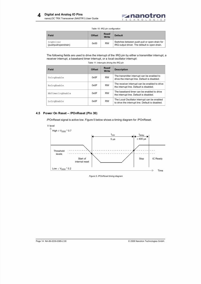
8/20/2019 nanoLOC NA5TR1 UserGuide
http://slidepdf.com/reader/full/nanoloc-na5tr1-userguide 30/325
Digital and Analog IO Pins
nanoLOC TRX Transceiver (NA5TR1) User Guide
Page 14 NA-06-0230-0385-2.00 © 2008 Nanotron Technologies GmbH.
4
The following fields are used to drive the interrupt of the IRQ pin by either a transmitter interrupt, a
receiver interrupt, a baseband timer interrupt, or a local oscillator interrupt:
4.5 Power On Reset – /POnReset (Pin 30)
/POnReset signal is active low. Figure 5 below shows a timing diagram for /POnReset.
Figure 5: /POnReset timing diagram
IrqDriver
(pushpull/opendrain)0x00 RW
Switches between push-pull or open-drain for
IRQ output driver. The default is open-drain.
Table 11: Interrupts driving the IRQ pin
Field OffsetRead/
WriteDescription
TxIrqEnable 0x0F RWThe transmitter interrupt can be enabled to
drive the interrupt line. Default is disabled.
RxIrqEnable 0x0F RWThe receiver interrupt can be enabled to drive
the interrupt line. Default is disabled.
BbTimerIrqEnable 0x0F RWThe baseband timer can be enabled to drive
the interrupt line. Default is disabled.
LoIrqEnable 0x0F RWThe Local Oscillator interrupt can be enabled
to drive the interrupt line. Default is disabled.
Table 10: IRQ pin configuration
Field OffsetRead/
WriteDefault
V level
Start of
internal reset
Time
tmin tdelay
Stop
Threshold
levels
High ≥ VDDD * 0.7
Low # VDDD * 0.2
5 µs ≥ 400 µs
IC Ready

8/20/2019 nanoLOC NA5TR1 UserGuide
http://slidepdf.com/reader/full/nanoloc-na5tr1-userguide 31/325
nanoLOC Clocking Structure
nanoLOC TRX Transceiver (NA5TR1) User Guide
© 2008 Nanotron Technologies GmbH. NA-06-0230-0385-2.00 Page 15
5
5 nanoLOC Clocking Structure
This section describes the four clocks provided by the nanoLOC chip: 32.768 kHz clock, SPI clock,
32 MHz baseband clock, and the Chirp Sequencer (CSQ) clock.
5.1 Overview
The nanoLOC chip provides the following four clocks:
32.786 kHz clock – Used to run the Real Time Clock and Power Management.
SPI clock – Used for the SPI Controller and for the Digital IO Control used for running the
four digital IO pins. The frequency of the SPI clock is dependent on the frequency required
by the microcontroller. The maximum frequency is 27 MHz.
32 MHz baseband clock – Used for baseband control, radio control, and other baseband
uses. The frequency of the baseband clock for the nanoLOC chip is 32 MHz and can be
enabled or disabled by software.
CSQ (Chirp Sequencer) Clock – Used by the Chirp Sequencer (CSQ) Memory. The fre-
quency of the CSQ clock is determined by dividing the Local Oscillator (LO) frequency by
10. The CSQ clock can be enabled or disabled by software.
Figure 6: nanoLOC clock structure
5.2 32.786 kHz Real Time Clock (RTC)
This Real Time Clock (RTC) runs at 32.768 kHz. It can be set or read through software using a 48
bit Real Time Clock value. As this clock is part of the ON section of the chip’s digital part, it is
always powered (unless the chip is completely powered off) and can, therefore, be used for creat-
ing a wake-up time event.
The Real Time Clock is also used to generate a 4 kHz clock (the Power Management clock) for use
by the Power Management module in the ON section. Like the Real Time Clock, this slow clock is
always available during power down mode to protect the connections between the SPI and the SPI
Controller.
Figure 7 below shows the Real Time Clock and Power Management modules that use the 32.768
kHz RTC.
Digital IO Control
ON PWD
DDDL Memory
SPI Controller
Real Time Clock
CSQ Memory
Others
Baseband Control
Radio Control
Power Management(4 kHz)
D[3:0]
Tx/Rx
SPI
µCirq
µCReset
µCVcc
Protection
32.786 kHz Clock:
SPI Clock:
32 MHz Baseband clock:
CSQ (Chirp Sequencer) Clock:

8/20/2019 nanoLOC NA5TR1 UserGuide
http://slidepdf.com/reader/full/nanoloc-na5tr1-userguide 32/325
nanoLOC Clocking Structure
nanoLOC TRX Transceiver (NA5TR1) User Guide
Page 16 NA-06-0230-0385-2.00 © 2008 Nanotron Technologies GmbH.
5
Figure 7: 32.786 kHz Real Time Clock
5.2.1 Updating and Reading the RTC Through Software
The 48 bit Real Time Clock is set and read through software. Since the Real Time Clock is updated
every 1/(32.768 kHz), it is not directly accessible by the user. A RAM buffer RamRtcReg is used to
hold the value of the internal Real time Clock after it has been read. This buffer is also used to hold
a value that will be written to the Real Time Clock.
Fields for Updating RTC by Software
The following fields are used for updating the Real Time Clock with software.
Updating the Value of the RTC
To update the value of the Real Time Clock, do the following
1 Write a 48 bit value for the Real Time Clock to the buffer RamRtcReg.
2 Write this buffer to the Real Time Clock using the write command RtcCmdWr.
Reading the Value of the RTC
To read the value of the Real Time Clock, do the following:
1 Read the Real Time Clock using the read command RtcCmdRd to place the 48 bit value of the
Real Time Clock in the buffer RamRtcReg.
2 Read out the buffer RamRtcReg.
5.2.2 Manually or Automatically Updating the RTC Using TimeB Packets
The Real Time Clock can also be updated from TimeB packets that have been sent from a base
station or other stations in a network. This updating can be performed automatically or manually.
If the updating is performed automatically, then when a TimeB packet is received, the RTC value in
the packet is automatically written to the Real Time Clock.
Table 12: RTC and TimeB packets
Field OffsetRead/
Write
Description
RtcCmdWr 0x62 WO Writes the 48 bit RTC value.
RtcCmdRd 0x62 WO Reads the 48 bit RTC value
RamRtcReg 0xF0 RW48 bit RTC value read from the RTC by software or writ-
ten to the RTC by software
ON PWD
Real Time Clock
Power Management(4 kHz)
D[3:0]
Tx/Rx
SPI
µCIRQ
µCReset
µCVcc
Protection
32.786 kHz Clock:

8/20/2019 nanoLOC NA5TR1 UserGuide
http://slidepdf.com/reader/full/nanoloc-na5tr1-userguide 33/325
nanoLOC Clocking Structure
nanoLOC TRX Transceiver (NA5TR1) User Guide
© 2008 Nanotron Technologies GmbH. NA-06-0230-0385-2.00 Page 17
5
If the updating is performed manually, then when a TimeB packet is received, the RTC value in the
packet must be manually updated as described in 5.2.1. Updating and Reading the RTC Through
Software on page 16.
Fields for Updating RTC by TimeB Packets
The following fields are used for updating the Real Time Clock by TimeB packets.
Manually Updating the RTC
To manually update the Real Time Clock through the RTC value in a TimeB packet, do the follow-
ing:
+ Enable manual mode for TimeB packets by setting:
RtcTimeBAutoMode = NA_RtcTimeBAutoModeOff_BC_C.
This causes the 48 bit RTC value in the received TimeB packets to be stored in the Real TimeClock buffer RamRtcReg, where it can then be written to the Real Time Clock using the write
command RtcCmdWr.
Automatically Updating the RTC
To automatically update the Real Time Clock through from the RTC value in a TimeB packet, do
the following:
+ Enable auto mode for TimeB packets by setting:
RtcTimeBAutoMode = NA_RtcTimeBAutoModeOn_BC_C.
This causes the RTC values in received TimeB packets to be automatically stored in the Real
Time Clock.
5.2.3 Using the RTC as Wake-Up Event
The Real Time Clock can be used to create a wake-up time event at a predefined time. The field
EnableWakeUpRtc enables the Real Time Clock to be used as a wake-up event.
The RTC wake-up time is set in RtcWakeUpTime but can only be accessed through the use of
WakeUpTimeByte and WakeUpTimeWe.
The wake-up time is a 24 bit value split into 3 bytes. The field WakeUpTimeByte is used to set
each of the three segments of the wake-up time (the segment to write is selected using the a byte-
selector field WakeUpTimeWe). This wake-up time value is then compared to bits 31 to 8 of theReal Time Clock. When these values match, a wake-up event is then triggered. This process is
shown in figure 8 below.
Table 13: RTC and TimeB packets
Field OffsetRead/
WriteDescription
RtcTimeBAutoMode 0x62 WOWhen set to 1, the RTC value is transferred in
TimeB packets
RtcTimeBRxAdj 0x61 WO Adjusts the RTC value for receiver delay.
RtcTimeBTxAdj 0x60 WO Adjusts the RTC value for transmitter delay
RamRtcTx 0xE0 RWThe 48 bit RTC value that is to be transmitted
(loaded/written) in a TimeB packet
RamRtcRx 0xE8 RWThe 48 bit RTC value that has been received in
a TimeB packet

8/20/2019 nanoLOC NA5TR1 UserGuide
http://slidepdf.com/reader/full/nanoloc-na5tr1-userguide 34/325
nanoLOC Clocking Structure
nanoLOC TRX Transceiver (NA5TR1) User Guide
Page 18 NA-06-0230-0385-2.00 © 2008 Nanotron Technologies GmbH.
5
Figure 8: Using Real Time Clock as wake-up event
Fields for Setting RTC as Wake-Up Event
The following fields are used for using the Real Time Clock as a wake-up time event.
5.3 SPI Clock
The SPI Clock is an externally delivered clock provided to the chip through an SPI signal from a
master device, such as a microcontroller. The frequency of the SPI clock is dependent on the fre-
quency of the master device. The maximum frequency of the SPI clock, however, is 27 MHz. It is
provided as one of the four signals of the SPI interface: SpiClk.
Figure 9 below shows the Digital IO Control and DDDL Memory modules as well as the SPI Con-
troller that use the SPI clock.
Figure 9: SPI Clock
Table 14: Wake-up time fields
Field OffsetRead/
WriteDescription
WakeUpTimeByte 0x01 WO
Stores a one byte value for the wake-up time,
which is programed to the wake-up time RtcWake-
UpTime using
WakeUpTimeWe.
WakeUpTimeWe 0x02 WO
Loads the value of RtcWakeUpTimeByte to the
appropriate byte of the wake-up time in the wake-
up time circuitry.
EnableWakeUpRtc 0x06 RW Enable Real Time Clock as Wake-Up Source
47 31 8
023
7 0
3 12
RtcWakeUpTime(RTC)
WakeUptime
WakeUptimeByteWe
WakeUptimeByte
0
Digital IO Control
ON PWD
DDDL Memory
SPI Controller
D[3:0]
Tx/Rx
SPI
µCIRQ
µCReset
µCVcc
SPI Clock:

8/20/2019 nanoLOC NA5TR1 UserGuide
http://slidepdf.com/reader/full/nanoloc-na5tr1-userguide 35/325
nanoLOC Clocking Structure
nanoLOC TRX Transceiver (NA5TR1) User Guide
© 2008 Nanotron Technologies GmbH. NA-06-0230-0385-2.00 Page 19
5
This clock is used to run the SPI Controller. As the Digital IO Control is run by the SPI Controller,
the SPI Clock is also used to run the four digital IO pins: D0, D1, D2, D3. It also runs all registers
that are written by the SPI Controller. In the Register Description tables, this is indicated in the
properties column of the register description (see 1.3.4. Field Properties Column on page 4).
5.4 32 MHz Baseband Clock
The baseband clock distribution obtains its frequency from the internal quartz oscillator. In the
nanoLOC chip, the internal quartz oscillator provides a 32 MHz frequency. This clock is used for
baseband control, radio control, and other baseband uses.
Figure 10: 32 MHz baseband clock
Note: The baseband clock can be enabled and disabled by software.
As the baseband clock is within the PWD section, this clock and all its modules run by this clock
are powered off when the chip goes into PowerDownModeFull. Consequently, the contents of all
chip registers are also lost.
Fields Related to the Baseband Clock
Stopping / Enabling the 32 MHz Baseband Clock
To reduce power consumption without losing the contents of chip registers, the baseband clock
distribution can be stopped and the quartz oscillator circuitry can be powered down.
The following block diagram shows the 32 MHz baseband clock and baseband quartz oscillator cir-
cuitry.
Table 15: Baseband clock related fields
Field OffsetRead/
WriteDescription
ResetBbClockGate 0x07 RW
Resets the baseband clock distribution cir-
cuitry.
ResetBbRadioCtrl 0x07 RWResets the digital baseband and radio control
circuitries.
EnableBbCrystal 0x08 RW Powers on the internal baseband oscillator.
EnableBbClock 0x08 RW Enable the baseband clock distribution.
ON PWD
Others
Baseband Control
Radio Control
32 MHz Baseband clock:
D[3:0]
Tx/Rx
SPI
µCIRQ
µCReset
µCVcc

8/20/2019 nanoLOC NA5TR1 UserGuide
http://slidepdf.com/reader/full/nanoloc-na5tr1-userguide 36/325
nanoLOC Clocking Structure
nanoLOC TRX Transceiver (NA5TR1) User Guide
Page 20 NA-06-0230-0385-2.00 © 2008 Nanotron Technologies GmbH.
5
Figure 11: Switching on/off the Baseband clock
Keeping Clock Switcher in Stable State
The clock switcher is kept in a stable state during warm-up and shut down of the quartz oscillator
by using ResetBbClockGate.
Stopping the 32 MHz Baseband Clock Distribution
To stop the baseband clock distribution, do the following:
1 Set EnableBbClock = False to switch off the baseband clock distribution.
2 Set ResetBbClockGate = True to enable active reset of the baseband clock circuitry.
3 Set EnableBbCrystal = False to power off the internal baseband quartz oscillator.
Enabling the 32 MHz Baseband Clock Distribution
To enable the baseband clock distribution, do the following:
1 Set EnableBbCrystal = True to power on the internal baseband quartz oscillator.
2 Set ResetBbClockGate = False to inactivate the reset of the baseband clock circuitry.
3 Set EnableBbClock = True to switch on the baseband clock distribution.
5.5 CSQ (Chirp Sequencer) Clock
The Chirp Sequencer clock (CSQ) is required for programming the Chirp Sequencer RAM mem-
ory. The frequency of the CSQ clock is determined by dividing the Local Oscillator (LO) frequency
by 10 (see 20.2. Calibrating the Local Oscillator Frequency on page 81). The CSQ clock can be
enabled or disabled by software using EnableCsqClock.
Figure 12 below shows the CSQ Memory module that uses the Chirp Sequencer clock.
Figure 12: Chirp Sequencer clock
IC boundary
CrystalOscillator
Clockgate
Internal powersupply bus
Step 3: EnableBbCrystal
Xtal32MP
Xtal32MN
32 MHz
Step 2: ResetBbClockGate
Step 1: EnableBbClock RSTRST
DEnable
Clock
Q
1
Baseband
clock
ON PWD
CSQ Memory
CSQ (Chirp Sequencer) Clock:
D[3:0]
Tx/Rx
SPI
µCIRQ
µCReset
µCVcc
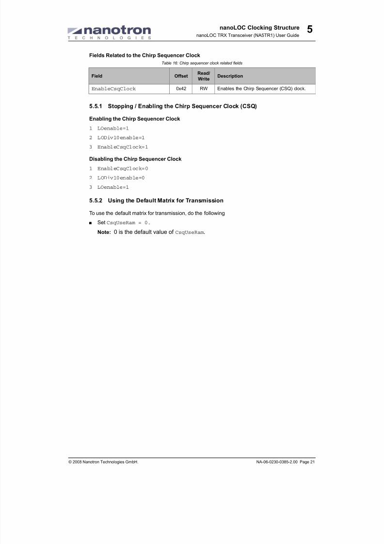
8/20/2019 nanoLOC NA5TR1 UserGuide
http://slidepdf.com/reader/full/nanoloc-na5tr1-userguide 37/325
nanoLOC Clocking Structure
nanoLOC TRX Transceiver (NA5TR1) User Guide
© 2008 Nanotron Technologies GmbH. NA-06-0230-0385-2.00 Page 21
5
Fields Related to the Chirp Sequencer Clock
5.5.1 Stopping / Enabling the Chirp Sequencer Clock (CSQ)
Enabling the Chirp Sequencer Clock
1 LOenable=1
2 LODiv10enable=1
3 EnableCsqClock=1
Disabling the Chirp Sequencer Clock
1 EnableCsqClock=0
2 LODiv10enable=0
3 LOenable=1
5.5.2 Using the Default Matrix for Transmission
To use the default matrix for transmission, do the following
+ Set CsqUseRam = 0.
Note: 0 is the default value of CsqUseRam .
Table 16: Chirp sequencer clock related fields
Field OffsetRead/
WriteDescription
EnableCsqClock 0x42 RW Enables the Chirp Sequencer (CSQ) clock.

8/20/2019 nanoLOC NA5TR1 UserGuide
http://slidepdf.com/reader/full/nanoloc-na5tr1-userguide 38/325

8/20/2019 nanoLOC NA5TR1 UserGuide
http://slidepdf.com/reader/full/nanoloc-na5tr1-userguide 39/325
Power Management
nanoLOC TRX Transceiver (NA5TR1) User Guide
© 2008 Nanotron Technologies GmbH. NA-06-0230-0385-2.00 Page 23
6
6 Power Management
This section describes the five power management states of the nanoLOC chip, which are
PwrDownModeFull, PwrDownModePad, PowerUp, Standby, and Ready.
The nanoLOC chip has been designed to efficiently use the power required to operate the chip.Modules required during transmission and reception, such as the baseband memory, CSQ mem-
ory, the SPI Controller, and other modules are located in a section of the chip that can be powered
down when not in use. To keep the chip operational, the minimum required modules are located in
a section of the chip that uses minimal power to maintain a connection with the microcontroller.
6.1 Power Management States
Table 17 shows the current consumption and activation time of the power management states.
6.2 Power Management Module – ON and PWD Sections
The Power Management module is located within a section called the “ON section.” It is provided
with a clock frequency of 4 kHz by the 32.768 kHz RTC. Figure 13 below shows the ON and PWD
sections of the nanoLOC chip, with the modules contained within each section. The connections
between the pins and the ON and PWD sections are shown as dashed lines, while connections
protected by the Power Management module protects are shown by the light lines.
Figure 13: Power Management Module
The Power Management module is responsible for maintaining the pull-up and pull-down states of
the SPI interface during all power down modes. This includes the pins: SpiClk, SpiSSn, SpiRxD,
and SpiTxD. This module is also responsible for maintaining the pull-up and pull-down states of several additional input/output pins, including:
+ /POnReset, an input pin which provides a signal to the power up reset line.
Table 17: Power management states
StateCurrent
Consumptiona
a. Current consumption values are typical values only.
Activation Time into State
PwrDownModeFull under 2.5 µAPowerUp: between 1 and 32 ms (programmable) + boot time
of the external microcontroller
PwrDownModePad # 600 µAPowerUp: between 1 and 32 ms (programmable) + boot time
of the external microcontroller
PowerUp # 700 µAStandBy: # 5 ms (depending on the speed of the baseband
quartz oscillator)
StandBy # 2.5 mA Ready (without reconfiguration) 6 µsb
b. @ 4 Mbit/s SPI.
Ready # 4 mA n./a.
Digital IO Control
ON PWD
DDDL Memory
SPI Controller
Real Time Clock
CSQ Memory
Others
Baseband Control
Radio Control
Power Management(4 kHz)
D[3:0]
Tx/Rx
SPI
µCIRQ
µCReset
µCVcc
Protection

8/20/2019 nanoLOC NA5TR1 UserGuide
http://slidepdf.com/reader/full/nanoloc-na5tr1-userguide 40/325
Power Management
nanoLOC TRX Transceiver (NA5TR1) User Guide
Page 24 NA-06-0230-0385-2.00 © 2008 Nanotron Technologies GmbH.
6
+ TxRx, an output pin which is used to control an external power amplifier.
+ µCReset, an output pin which resets an external microcontroller.
+ µCIRQ, an output pin which sends interrupt requests to an external microcontroller.
The Digital IO pins are always powered as they can be programmed to provide a wake-up event to
bring the PWD section back to powered up state.
6.3 Power Management State Model
The power management states model of the nanoLOC chip is shown below.
Figure 14: Power management state model
6.4 Power Management Fields
The following fields are used for Power Management:
Receive Mode
Internal basebandclock distribution off
Internal basebandclock distribution on
Configuration ofWake Up Timers or
of alarm Events
Configuration ofWake Up Timers or
of alarm Events
TX-INIT
TX RF-INIT
Calibrate-TX
Transmit Mode
RX-INIT
RX RF-INIT
Calibrate-RX
Station-INIT
Ready Mode
Standby Mode
Baseband quartzclock off
Baseband quartzclock on
Powerup Mode
Wake-up timeror alarm events
Wake-up timeror alarm events
PowerdownPAD Mode
PowerdownFULL Mode
Table 18: Power management related fields
Field Offset Description
EnableWakeUpRtc 0x06 RTC wake-up event brings the chip into the power up state.
EnableWakeUpDio 0x06 Alarm event (rising/falling edge) at a digital IO configured as a wake-up
source (see register 0x4) brings the chip into the power up state.
PowerUpTime 0x06 Configures duration of the power-up time (duration of active µCReset).
PowerDownMode 0x06Selects the power down mode to use when the chip enters the powered
down state
PowerDown 0x07Brings the chip to the configured power-down state. This bit will be
automatically cleared when the chip is powered-up.

8/20/2019 nanoLOC NA5TR1 UserGuide
http://slidepdf.com/reader/full/nanoloc-na5tr1-userguide 41/325
Power Management
nanoLOC TRX Transceiver (NA5TR1) User Guide
© 2008 Nanotron Technologies GmbH. NA-06-0230-0385-2.00 Page 25
6
6.5 PowerDownModeFull State
When the chip is in PowerDownModeFull, it consumes less power but after power up the chip will
need to be reconfigured. The pins and registers of the chip are powered off but reconfiguration of
the registers is required after wake-up. Also leakage current is the lowest possible in this mode.
Figure 15: PowerDownModeFull showing powered sections
Current Consumption: The current consumption1 during PowerDownModeFull is under 2.5 µA.
Chip State: The chip is in the following state during PowerDownModeFull:
Setting PowerDownModeFull: To set PowerDownModeFull, do the following:
1 Set PowerDownMode = NA_PowerDownModeFull_C (0x0)
2 Set PowerDown = 1
Bringing to PowerUp State: Either an internal wake-up timer or an external event on a Digital IO
pin brings the chip out of PowerDownModeFull into PowerUp state. This activation time is pro-
grammable using the field PowerUpTime in a range between 1 and 32 ms + boot time of the exter-
nal microcontroller. After the chip is in PowerUp mode, the external microcontroller can then
initialize and (optionally) calibrate the chip.
1. Current consumption values are typical values only and are values without an external microcontroller
and where digital IO pads are tri-state or inputs and no external pull-up resistors soldered on pads.
Table 19: PowerDownModeFull state
Module State
External Microcontroller (µcVcc) Powered down
PWD section Powered down (all register settings lost)
ON section Powered
Real Time Clock Running
Wake-up timer Running
Digital IO Control Running
Power Management module Running
Digital IO Control
ON PWD
DDDL Memory
SPI Controller
Real Time Clock
CSQ Memory
Others
Baseband Control
Radio Control
Power Management(4 kHz)
Protection
Powered =
D[3:0]
Tx/Rx
SPI
µCIRQ
µCReset
µCVcc

8/20/2019 nanoLOC NA5TR1 UserGuide
http://slidepdf.com/reader/full/nanoloc-na5tr1-userguide 42/325
Power Management
nanoLOC TRX Transceiver (NA5TR1) User Guide
Page 26 NA-06-0230-0385-2.00 © 2008 Nanotron Technologies GmbH.
6
6.6 PowerDownModePad State
When the chip is in PowerDownModePad, it consumes more power than PowerDownModeFull but
after it has been powered up, it does not need to be reconfigured. In this state, all output pads are
disabled and all bi-directional pads are switched to input, but all transceiver registers are still pow-
ered. Reconfiguration of the chip registers is not required, but leakage current is higher.
Figure 16: PowerDownModePad showing powered sections
Current Consumption: The current consumption during PowerDownModePad state is approxi-
mately 600 µA.
Chip State: The chip is in the following state during PowerDownModePad:
Setting PowerDownModePad: To set PowerDownModePad, do the following:
1 Set PowerDownModePAD = NA_PowerDownModePad_C (0x1)
2 Set PowerDown = 1
Bringing to PowerUp State: Either an internal wake-up timer or an external event on a Digital IO
pin brings the chip out of PowerDownModePad. The chip then goes into PowerUp state. The acti-
vation time is programmable using the field PowerUpTime in a range between 1 and 32 ms + boot
time of the external microcontroller. After the chip is set in Ready state, the external microcontroller
can then initialize and calibrate the chip.
Table 20: PowerDownModePad state
Module State
External Microcontroller (µcVcc) Powered down
PWD section Powered (all register settings maintained)
ON section Powered
Real Time Clock Running
Wake-up timer Running
Digital IO Control Running
Power Management module Running
Digital IO Control
ON PWD
DDDL Memory
SPI Controller
Real Time Clock
CSQ Memory
Others
Baseband Control
Radio Control
Power Management(4 kHz)
Protection
Powered =
D[3:0]
Tx/Rx
SPI
µCIRQ
µCReset
µCVcc

8/20/2019 nanoLOC NA5TR1 UserGuide
http://slidepdf.com/reader/full/nanoloc-na5tr1-userguide 43/325
Power Management
nanoLOC TRX Transceiver (NA5TR1) User Guide
© 2008 Nanotron Technologies GmbH. NA-06-0230-0385-2.00 Page 27
6
6.7 PowerUp State
The chip enters PowerUp state from either PowerDownModeFull or PowerDownModePad through
on of the following: internal wake-up timer, external event on a Digital IO pin, or an external reset
Figure 17: PowerUp state
Current Consumption: The current consumption during Powerup state is approximately 700 µA.
Chip State: When the chip is brought to PowerUp state, the following occurs:
Bringing to Standby State: When the chip is brought from PowerUp state into Standby state, all
blocks are powered up except the baseband distribution, which remains switched off. The activa-
tion time to bring the chip into Standby state from PowerUp state is approximately 5 ms, depending
on the speed of the baseband quartz oscillator.
Wake-Up Sources for PowerUp State: The chip is brought to PowerUp state by a wake-up
source. This is either a RTC wake-up event or an alarm event (a rising or falling edge) at one of the
digital IOs configured as a wake-up source. Table 22 lists the fields used to set a wake-up event.
Table 21: PowerUp state
Module State
External Microcontroller (µcVcc) Powered
From PowerDownModeFull to PowerUp PWD section powered and all pins are enabled
From PowerDownModePad to PowerUp All output pins are enabled and digital IO pins are switchedto bi-directional
Real Time Clock, Wake-up timer, and Power
Management moduleRunning
Internal baseband quartz oscillator Powered on and then baseband clock distribution is
switched off
Internal baseband modulesInitiailzed with default settings and can now be programmed
via the SPI interface
Table 22: Fields for setting a wake-up event
Field Offset Description
EnableWakeUpRtc 0x06 Enable the Real Time Clock as a wake-up source. Default is disabled.
EnableWakeUpDio 0x06 Enable a digital IO pin as a wake-up source. Default is disabled.
Digital IO Control
ON PWD
DDDL Memory
SPI Controller
Real Time Clock
CSQ Memory
Others
Baseband Control
Radio Control
Power Management(4 kHz)
Protection
Powered =
D[3:0]
Tx/Rx
SPI
µCIRQ
µCReset
µCVcc

8/20/2019 nanoLOC NA5TR1 UserGuide
http://slidepdf.com/reader/full/nanoloc-na5tr1-userguide 44/325
Power Management
nanoLOC TRX Transceiver (NA5TR1) User Guide
Page 28 NA-06-0230-0385-2.00 © 2008 Nanotron Technologies GmbH.
6
6.8 Standby State
When the chip is In Standby state, only the baseband clock distribution is switched off. All other
blocks of the chip are fully powered.
Figure 18: Standby state
Current Consumption: The current consumption during Standby state is approximately 2.5 mA.
Bringing to Ready State: To bring the chip into Ready state, the baseband clock distribution is
switched on. Activation time to bring the chip into Standby mode from PowerUp mode is 6 µs @
4 Mbit/s SPI (without reconfiguration).
6.9 Ready State
When the chip is In Ready State, the baseband clock distribution is switched on and the microcon-
troller can immediately initiate a packet transmission or reception.
Figure 19: Ready state
Current Consumption: The current consumption during Ready Mode is approximately 4 mA.
6.10 Powering Off the Chip
When the chip is completely powered off, which is when the power source is disconnected from the
chip, both the ON and PWD sections are powered off and all chip settings are lost. The connectionbetween the microcontroller (master device) and the chip (slave device) are lost and the Local
Oscillator will require recalibration.
Digital IO Control
ON PWD
DDDL Memory
SPI Controller
Real Time Clock
CSQ Memory
Others
Baseband Control
Radio Control
Power Management(4 kHz)
Protection
Powered =
D[3:0]
Tx/Rx
SPI
µCIRQ
µCReset
µCVcc
Digital IO Control
ON PWD
DDDL Memory
SPI Controller
Real Time Clock
CSQ Memory
Others
Baseband Control
Radio Control
Power Management(4 kHz)
D[3:0]
Pamp
SPI
µCirq
µCReset
µCVcc
Protection
Powered =

8/20/2019 nanoLOC NA5TR1 UserGuide
http://slidepdf.com/reader/full/nanoloc-na5tr1-userguide 45/325
nanoLOC Programming Interface (SPI)
nanoLOC TRX Transceiver (NA5TR1) User Guide
© 2008 Nanotron Technologies GmbH. NA-06-0230-0385-2.00 Page 29
7
7 nanoLOC Programming Interface (SPI)
This section describes the programming interface (SPI) to the nanoLOC chip, including descrip-
tions of the SPI Controller, signals, interface connections, timing, and address format.
The nanoLOC chip is programmed through the use of a synchronous Serial Peripheral Interface
(SPI) interface. This SPI interface is used to write control bits into memory locations in the chip reg-
ister and baseband RAM locations. The SPI communicates via the SPI bus between a master
device, such as a microcontroller, and one or more slave devices, including the nanoLOC chip and
any serial memory devices.
7.1 SPI Controller
All SPI requests are distributed through the SPI Controller, whether in the PWD section or the ON
section of the nanoLOC chip. In particular, the SPI Controller, which uses the SPI clock, directs SPI
requests to the appropriate registers. All registers written by the SPI Controller are run with SPI
clock, with the exception of Read Only registers.
Note: SPI requests are only possible when the PWD section of the chip is powered, as the SPI
Controller is located in this section. See 7.1.1. SPI Controller and Power Management on
page 29.
Figure 20 below shows the flow of SPI requests in the PWD and On sections of the nanoLOC chip.
Figure 20: nanoLOC SPI Controller
7.1.1 SPI Controller and Power Management
PowerdownModeFull: When the chip is in PowerdownModeFull state the PWD section is com-
pletely powered down to reduce chip power consumption, which means all register settings are
lost. However, the ON section retains a small amount of power to save specific chip settings
related to the Digital IO pins, the Real Time Clock, and Power Management. Also, the connections
between a microcontroller and the SPI Controller is protected to enable the chip to quickly wake-up
and to be fully operational in a very short time.
PowerDownModePad: When the chip is in PowerDownModePad state, the PWD section remains
powered, which means all register settings are maintained.
PowerUp: When the chip is in PowerUp state, the connection between the microcontroller and the
SPI Controller over the SPI bus is quickly reestablished. Then, depending on what power downstate was set, the microcontroller then initializes the registers in the PWD section and (optionally)
calibrates the Local Oscillator frequency.
ON PWD
D[3:0]
SPI
Others
Baseband Control
Radio Control
SPI Controller
Digital IO Control
Real Time Clock
SPI Requests
Power Management(4 kHz)
Protection

8/20/2019 nanoLOC NA5TR1 UserGuide
http://slidepdf.com/reader/full/nanoloc-na5tr1-userguide 46/325
nanoLOC Programming Interface (SPI)
nanoLOC TRX Transceiver (NA5TR1) User Guide
Page 30 NA-06-0230-0385-2.00 © 2008 Nanotron Technologies GmbH.
7
7.1.2 SPI Controller and Registers
The SPI Controller contains a mirror of the registers in the ON part. This is done to save power as
less connections are maintained between the ON and PWD parts, especially for those registers
relating to Digital IO control.
The SPI Controller also include those registers that must be accessible when the baseband clock
is off, including:
+ Pad controls – For example, registers for the SPI direction (MSB/LSB).
+ Clock controls – For example, registers for enabling for baseband clock.
+ Constants – For example, registers for the chip version and revision number.
7.2 SPI Bit Ordering
The SPI bit order of the nanoLOC chip is configurable, either LSB (Least Significant Bit First) or
MSB (Most Significant Bit First). To set the bit order for the SPI bus, use the field SpiBitOrder,where:
+ SpiBitOrder = 1: the first bit transmitted over the SPI is MSB.
+ SpiBitOrder = 0: the first bit transmitted over the SPI is LSB.
The default bit order after reset or power-up is LSB first. Table 23 below lists the field used to set
the SPI bit order.
Note: The byte order always remains the same.
7.3 SPI Signals: SpiClk, SpiSsn, SpiTxD, SpiRxD
The SPI interface works as a half-duplex channel and uses the following four signals:
+ SPI Clock – SpiClk
This is a clock signal applied by the microcontroller (master device).
+ SPI Slave Select – /SpiSsn
This signal is used by the microcontroller (master device) to select the nanoLOC chip (slave
device) for communication.
Note: This signal is specific to only one slave.
+ Data Transmit – SpiTxD
This signal is MISO (Master – Input; Slave – Output). With this signal, data is sent from a slave
device (such as the nanoLOC chip or other slave devices) to a master device (microcontroller).
SpiTxD is programmable as either push-pull or open-drain pin. When more than one slave
device is connected to the SPI bus, the SpiTxD pin should be set to open drain mode. See also
7.4. SPI TxD Output Driver on page 31.
Note: In open drain mode an external pull up resistor is required.
+ Data Receive – SpiRxD
This signal is MOSI (Master – Output; Slave – Input). With this signal, data is sent from a mas-ter device (microcontroller) to a slave device (such as the nanoLOC chip or other slave
devices).
Table 23: Bit order fields
Field Offset Description
SpiBitOrder (MSB/LSB first) 0x00 Sets the bit order for the SPI bus. Default is LSB.

8/20/2019 nanoLOC NA5TR1 UserGuide
http://slidepdf.com/reader/full/nanoloc-na5tr1-userguide 47/325
nanoLOC Programming Interface (SPI)
nanoLOC TRX Transceiver (NA5TR1) User Guide
© 2008 Nanotron Technologies GmbH. NA-06-0230-0385-2.00 Page 31
7
7.4 SPI TxD Output Driver
The SPI TxD Output Driver can be set as either push-pull or open-drain by using SpiTxDriver.
Open-Drain: In this setting, the pad is driven only when a logic 0 is sent from the nanoLOC chip tothe SPI master. Otherwise, the output is in high-impedance state. Do the following to set the SPI
TxD output driver to open-drain:
+ SpiTxDriver = 0
Push-Pull: The pad is driven in push-pull mode, but only when data is sent from the nanoLOC chip
to the SPI master. Otherwise, the output is in high-impedance state. Do the following to set the SPI
TxD output driver to push-pull:
+ SpiTxDriver = 1
Default value: The default value is SpiTxDriver = 0 (false).
Table 24 below lists the field used to switch the TxD output driver between push-pull and open-
drain.
7.5 SPI Bus Timing Values
The following table lists the timing values for the SPI bus:
7.6 SPI Transfer Rate
7.6.1 Maximum Transfer Rate
The maximum transfer rate for communication between the microcontroller (the master device)
and the nanoLOC chip (the slave device) is 27 MBit/s.
7.6.2 Bytes Per Transfer
For each SPI transfer, between 3 and 130 bytes (1-128 data bytes) can be sent per transfer.
Table 24: SPI TxD Output driver field
Field Offset Description
SpiTxDriver 0x00Switches between push-pull and open-drain for the TxD output driver
(SpiTxD - pin 17).
Table 25: SPI bus timing values
Parameter Minimum Maximum Description
f max – 27 MHz SpiClk
tLC 18.5 ns – Low time SpiClk
tHC 18.5 ns – High time SpiClk
tSS 4 ns – /SpiSsn Setup
tHS 2 ns - /SpiSsn Hold
tSRxD 4 ns – SpiRxD Setup
tHRxD 2 ns – SpiRxD Hold
tPDTxD – 18.5 ns SpiTxD Propagation Delay Drive
tHTxD 2.5 ns – SpiTxD Hold
tPTxDZ – 18.5 ns SpiTxD Propagation Delay High Impedance
8/20/2019 nanoLOC NA5TR1 UserGuide
http://slidepdf.com/reader/full/nanoloc-na5tr1-userguide 48/325
nanoLOC Programming Interface (SPI)
nanoLOC TRX Transceiver (NA5TR1) User Guide
Page 32 NA-06-0230-0385-2.00 © 2008 Nanotron Technologies GmbH.
7
7.7 SPI Interface Connections
The nanoLOC chip can be wired with an SPI master device with a four-wire, a three-wire, or multi-
ple-slave configuration.
7.7.1 Four-Wire Configuration
Four-wire configuration is the standard configuration between the nanoLOC chip (slave) and a
microcontroller (master). It requires all four lines of the SPI interface, as illustrated in figure 21.
Figure 21: Four-wire option of the SPI
7.7.2 Three-Wire Configuration
If only a single nanoLOC chip (slave) is connected to the microcontroller (master), then the SpiSSn
input pin can be connected to GND, as illustrated in figure 22.
Figure 22: Three-wire option of the SPI
This configuration saves one pin on the SPI master device or makes the pin available for other
functions. This saves space on a circuit board, which is significant since many applications using
the nanoLOC chip require a small form factor. Also, if the SpiSSn pin is driven with an active-low
voltage level permanently, the power consumption of the nanoLOC chip is not increased.
7.7.3 Multiple Slave Configuration
If multiple slave devices (for example, multiple nanoLOC chips) are controlled by a single master
device, the /SpiSSn pin of each slave device is connected to the SSN pin on the master device.
Figure 23: Multiple slave connection
nanoLOC(Slave)
Microcontroller (Master)
CLK
TxD
RxD
/CS1 (SSN)
SpiClk
SpiRxD
/SpiSSn
SpiTxD
MOSI
MISO
nanoLOC(Slave)
Microcontroller (Master)
CLK
TxD
RxD
SpiClk
SpiRxD
/SpiSSn
SpiTxD
MOSI
MISO
nanoLOC(Slave 1)
Slave n
Microcontroller (Master)
CLK
TxD
RxD
/CS1 SSN0
SpiClk
SpiRxD
/SpiSSn
SpiTxD
Clk
RxD
/CS
TxD
/CSn SSN1
MOSI
MISO
pull-up resistor
...
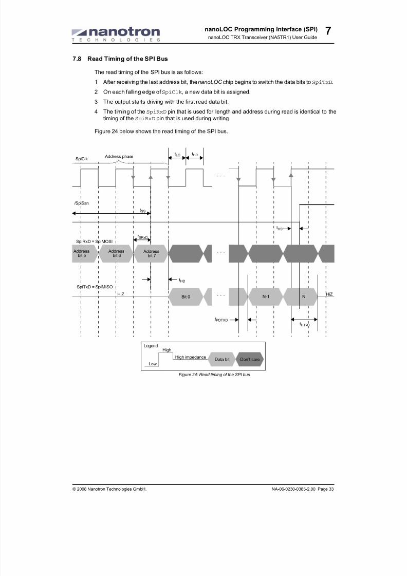
8/20/2019 nanoLOC NA5TR1 UserGuide
http://slidepdf.com/reader/full/nanoloc-na5tr1-userguide 49/325
nanoLOC Programming Interface (SPI)
nanoLOC TRX Transceiver (NA5TR1) User Guide
© 2008 Nanotron Technologies GmbH. NA-06-0230-0385-2.00 Page 33
7
7.8 Read Timing of the SPI Bus
The read timing of the SPI bus is as follows:
1 After receiving the last address bit, the nanoLOC chip begins to switch the data bits to SpiTxD.
2 On each falling edge of SpiClk, a new data bit is assigned.
3 The output starts driving with the first read data bit.
4 The timing of the SpiRxD pin that is used for length and address during read is identical to the
timing of the SpiRxD pin that is used during writing.
Figure 24 below shows the read timing of the SPI bus.
Figure 24: Read timing of the SPI bus
tHS
/SpiSsn
tLC tHC
tSS
tSRxD
tHTxD
tHD
. . .
SpiRxD = SpiMOSI
Address bit 7
SpiTxD = SpiMISO
Bit 0 N-1 N. . . HiZHiZ
Address phaseSpiClk
Address bit 6
Address bit 5
tPDTXD
. . .
Legend
Low
High
High impedanceData bit Don’t care

8/20/2019 nanoLOC NA5TR1 UserGuide
http://slidepdf.com/reader/full/nanoloc-na5tr1-userguide 50/325
nanoLOC Programming Interface (SPI)
nanoLOC TRX Transceiver (NA5TR1) User Guide
Page 34 NA-06-0230-0385-2.00 © 2008 Nanotron Technologies GmbH.
7
7.9 Write Timing of the SPI Bus
The write timing of the SPI bus is as follows:
1 On the first falling edge of the clock signal (SpiClk), with the master device SPI slave select (/
SpiSsn) being low, the first data bit is switched (sent) to
SpiRxD.
2 As long as /SpiSsn is activated, the nanoLOC chip latches one data bit onto each rising edge
of the clock signal (SpiClk).
3 If several slave devices share the SPI bus, then the master device must control the communi-
cation with slave-dedicated chip selects (/SpiSsn(n)).
4 To complete an operation to a specific SPI slave, the /SpiSsn signal must be set to high after
the last data bit has been transmitted.
Figure 25 below shows the write timing of the SPI bus.
Figure 25: Write timing of the SPI bus
SpiClk
. . .tHS
/SpiSsn
tLC tHC
tSS
tSRxD
tHRxD
tHD
. . .
SpiRxD
31 ns
Bit 0 Bit N
Legend
Low
High
High impedanceData bit Don’t care
. . .

8/20/2019 nanoLOC NA5TR1 UserGuide
http://slidepdf.com/reader/full/nanoloc-na5tr1-userguide 51/325
nanoLOC Programming Interface (SPI)
nanoLOC TRX Transceiver (NA5TR1) User Guide
© 2008 Nanotron Technologies GmbH. NA-06-0230-0385-2.00 Page 35
7
7.10 SPI Address Format
The SPI of the nanoLOC chip implements a burst capable address mode with automatic address
increment. The SPI protocol has a variable data payload. Figure 26 below shows the SPI transfer
format.
Figure 26: SPI transfer format
7.10.1 Byte 1: Instruction
The <Instruction> field has a fixed length of one byte and contains the command type
(read[0] / write[1]) as well as the number of data bytes:
+ Bit 7 is the “direction bit” and is used to differentiate between read or write access, where:
+ Write access = 1
+ Read access = 0
+ Bits 0 to 6 provides the data byte size. This is the size of data that will be sequentially written to
the nanoLOC chip or read from the nanoLOC chip in an access operation. The maximumlength is 128 bytes, which is indicated by a 0x00 value.
7.10.2 Byte 2: Address
The <Address> field has a fixed length of one byte and contains the first address to be accessed.
Additional data bytes are accessed at the addresses that follow the address provided here.
If the data payload is greater than one, the interface is used in burst mode with automatic address
increment.
7.10.3 N Bytes: Data Payload
The <Data Payload> field has a size (N) and can vary from one byte to 128 bytes. It contains the
data that is to be written to or read from the target register(s).
MSB LSB
7 6 5 4 3 2 1 0
Direction Bit Data Bytes Size
MSB LSB
7 6 5 4 3 2 1 0
Address Byte
MSB LSB
7 6 5 4 3 2 1 0
Data Payload
...
Data Payload
Length
Start Address
Data
Byte 1: <Instruction>
Byte 2: <Address>
Byte N: 3 ≤ <N byte data> ≤ 130
RW

8/20/2019 nanoLOC NA5TR1 UserGuide
http://slidepdf.com/reader/full/nanoloc-na5tr1-userguide 52/325
nanoLOC Programming Interface (SPI)
nanoLOC TRX Transceiver (NA5TR1) User Guide
Page 36 NA-06-0230-0385-2.00 © 2008 Nanotron Technologies GmbH.
7
7.11 SPI Read Operations
To read data from the nanoLOC chip, do the following:
1 In the <Instruction> field, set the direction bit to the value 0 (read data) and set the data
size, where the maximum size is 128.
2 In the <Address> field, set the source address.
3 Send the <Instruction> and <Address> data to the slave device(s).
4 Read in the resultant data from the slave device(s).
Figure 27 below shows the timing of a read operation.
Figure 27: Read Access (LSB first)
Note: The SpiTxD pin is activated into push-pull or open-drain mode only if the data payload
bytes are transmitted and if the slave device is selected through SpiSsn. Otherwise, the
SpiTxD pin is always in the high impedance state.
7.12 SPI Write Operations
To write data to the nanoLOC chip, do the following:
1 In the <Instruction> field, set the direction bit to the value 1 (write data) and set the data
size, where the maximum size is 128.
2 In the <Address> field, set destination address.
3 In the <Data Payload> field, set the data that will be written to the slave device(s).
4 Send the <Instruction>, <Address>, and <Data Payload> data to the slave device(s).
The timing of a write operation is shown in the following figure:
Figure 28: Write access (LSB first)
Note: During a write operation the SpiTxD pin is always in the high impedance state.
Length R
0 7 70
ADDR
SpiTxD
SpiRxD
70 70 70
Data 0 Data 1 . . .
/SpiSsn
Legend
Low
High
High impedanceData bit Don’t care
Length W
0 7 70 70 70 70
ADDR Data 0 Data 1
/SpiSsn
SpiRxD. . .
Legend
Low
High
High impedanceData bit Don’t care

8/20/2019 nanoLOC NA5TR1 UserGuide
http://slidepdf.com/reader/full/nanoloc-na5tr1-userguide 53/325
nanoLOC Programming Interface (SPI)
nanoLOC TRX Transceiver (NA5TR1) User Guide
© 2008 Nanotron Technologies GmbH. NA-06-0230-0385-2.00 Page 37
7
7.12.1 Write Access Example
The following shows a write access example where three bytes (0x11, 0x22 and 0x33) are written
to three registers that start at the address location 0x23:
Instruction field: First, the chip needs to know if this request is a read or write command, and how
many bytes of data will be written to the register(s). In this example, the <Instruction> field has
a value of <0x83>, which has a binary value of 10000011, as shown below:
The bit direction is set to write with three bytes of data to follow that are to be written.
Address field: Next, the chip needs to know to where in the register these three bytes of data are
to be written (that is, which offset address to point to). In this example, the <Address> field has a
value of <0x23>, which has a binary value of 00100011, as shown below:
The data bytes are be written beginning at the offset address 0x23.
N data fields (3 bytes): Finally, include the data to be written beginning at the offset address 0x23.
In this example, the <Data Payload> field has the values 0x11, 0x22, and 0x33, which have the
binary values 00010001, 00100010, and 00110011, respectively, as shown in the following dia-
gram:
The three values 00010001, 00100010, and 00110011 will be written to the chip registers begin-
ning at offset address 0x23, that is offset addresses 0x23, 0x24, and 0x25.
Figure 29 below shows the location of the three registers in the chip register where the data pro-
vided has been written.
MSB LSB
7 6 5 4 3 2 1 0
1 0 0 0 0 0 1 1
Write
AccessNumber of Bytes = 3
MSB LSB
7 6 5 4 3 2 1 0
0 0 1 0 0 0 1 0
Address location = 0x23
MSB LSB
7 6 5 4 3 2 1 0
0 0 0 1 0 0 0 1
0 0 1 0 0 0 1 0
0 0 1 1 0 0 1 1
<0x83><0x23><0x11><0x22><0x33>
Instructionfield
Addressfield
Data payloadfield
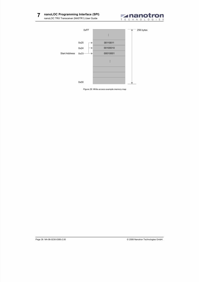
8/20/2019 nanoLOC NA5TR1 UserGuide
http://slidepdf.com/reader/full/nanoloc-na5tr1-userguide 54/325
nanoLOC Programming Interface (SPI)
nanoLOC TRX Transceiver (NA5TR1) User Guide
Page 38 NA-06-0230-0385-2.00 © 2008 Nanotron Technologies GmbH.
7
Figure 29: Write access example memory map
0xFF
0x23
0x00
Start Address
00110011
00100010
00010001
.
.
.
256 bytes
0x24
0x25
.
.
.

8/20/2019 nanoLOC NA5TR1 UserGuide
http://slidepdf.com/reader/full/nanoloc-na5tr1-userguide 55/325
nanoLOC Memory Map
nanoLOC TRX Transceiver (NA5TR1) User Guide
© 2008 Nanotron Technologies GmbH. NA-06-0230-0385-2.00 Page 39
8
8 nanoLOC Memory Map
This section describes the memory map of the nanoLOC chip. Procedures are provided for
accessing the chip’s programmable Register Block, as well the Baseband RAM, Chirp Sequencer
RAM, and Correlator RAM. Figure 30 below shows the memory map of the nanoLOC chip.
Figure 30: nanoLOC memory map
The nanoLOC memory map provides the following sections:
Table 26: nanoLOC memory map section
Hex Value Memory Type Description
0x000 to 0x3FF Baseband RAM
512 bytes of Baseband RAM stores both data payload and
MAC header values, depending on buffer configuration set-
tings.
0x800 to 0xBFF Chirp SequencerRAM
Delivers two sequences of 6-bit values that synthesize the Iand Q signals of a symbol.
Address
Memory
TypePage Select
Register
Select Bits 6-0
11-10 9-8 7
Hex FFF
11
11
1 Correlator RAM Page 3
0 Register Block
10
1 Correlator RAM Page 2
0 Register Block
01
1 Correlator RAM Page 1
0 Register Block
00
1 Correlator RAM Page 0
Hex C00 0 Register Block
Hex BFF
10
11
1 Chirp Sequencer Page 3
0 Register Block
10
1 Chirp Sequencer Page 2
0 Register Block
01
1 Chirp Sequencer Page 1
0 Register Block
00
1 Chirp Sequencer Page 0
Hex 800 0 Register Block
Hex 7FF01
Hex 400
Hex 3FF
00
11
1 Baseband Page 3
0 Register Block
10
1 Baseband Page 2
0 Register Block
01
1 Baseband Page 1
0 Register Block
00
1 Baseband Page 0
Hex 000 0 Register Block
C o r r e
l a t o r
R A M
C h i r p S e q u e n c e r
B a s e
b a n
d R A M
U n u s e
d

8/20/2019 nanoLOC NA5TR1 UserGuide
http://slidepdf.com/reader/full/nanoloc-na5tr1-userguide 56/325
nanoLOC Memory Map
nanoLOC TRX Transceiver (NA5TR1) User Guide
Page 40 NA-06-0230-0385-2.00 © 2008 Nanotron Technologies GmbH.
8
Note: For a description of the Chirp Sequencer, see 9. Chirp Sequencer (CSQ) on page 45. The
Correlator RAM is described in 8.3. Correlator RAM Access on page 43. The Register Block
is described in 8.2. 128 Byte Programmable Register Block on page 42.
8.1 Selecting a Memory Address
Two SPI accesses to the nanoLOC chip are required to select a memory address in the chip’s
memory map. This is because the SPI uses 8 bits for read or write access while 12 bits are
required to select a memory address.
8.1.1 First SPI Access
On the first SPI access, the four upper address bits are accessed, as shown in figure 31 below.
Figure 31: First SPI access
This first SPI write transfer is divided into the following two parts:
1 Select Memory type:
One of the three memory types is selected by setting the address bits 11 and 10, which is the
field DeviceSelect. This selects one of Baseband RAM, Chirp Sequencer RAM, or Correla-
tor RAM.
Note: One of the four memory spaces is unused.
2 Select page:
One of the four pages in the selected memory type is chosen by setting the address bits 9 and
8, which is the field RamIndex.
DeviceSelect and RamIndex are shown in a 12 bit SPI access in figure 32 below.
Figure 32: DeviceSelect and RamIndex on first SPI write transfer
Note: See Register 26.16. 0x0E – Baseband Memory Access on page 139
0xC00 to 0xFFF Correlator RAM
Stores the reference and threshold values for detection. It is
are initialized with the FDMA, 4 µs default detector matrix.
When other symbols are needed this register must be pro-grammed with the appropriate values. The threshold must be
programmed with the appropriate value in any case (even for
the default matrix).
0x000 to 0x07F Register Block
128 byte programmable chip register block provides chip
configuration settings and is mapped to the entire memory of
the nanoLOC chip.
Table 26: nanoLOC memory map section
Hex Value Memory Type Description
Address
Device
SelectRam Index
Register
Select Bits 6-0
11-10 9-8 7
Hex addressone of 00, 01,
10, or 11one of 00, 01,
10, or 11
1 RAM Location
Hex address 0 Register Block
First SPI access
11 10 9 8 7 6 5 4 3 2 1 0
0 0 0 0 1 0 1 1 1 1 1 0
RamIndex
Page selectMemory type
DeviceSelect
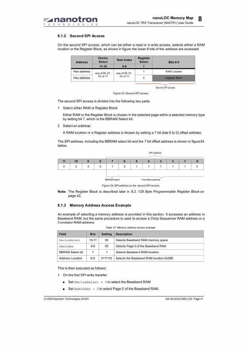
8/20/2019 nanoLOC NA5TR1 UserGuide
http://slidepdf.com/reader/full/nanoloc-na5tr1-userguide 57/325
nanoLOC Memory Map
nanoLOC TRX Transceiver (NA5TR1) User Guide
© 2008 Nanotron Technologies GmbH. NA-06-0230-0385-2.00 Page 41
8
8.1.2 Second SPI Access
On the second SPI access, which can be either a read or a write access, selects either a RAM
location or the Register Block, as shown in figure the lower 8 bits of the address are accessed.
Figure 33: Second SPI access
The second SPI access is divided into the following two parts:
1 Select either RAM or Register Block:
Either RAM or the Register Block is chosen in the selected page within a selected memory type
by setting bit 7, which is the BBRAM Select bit.
2 Select an address:
A RAM location or a Register address is chosen by setting a 7 bit (bits 6 to 0) offset address.
The SPI address, including the BBRAM select bit and the 7 bit offset address is shown in figure 34
below.
Figure 34: SPI address on the second SPI access
Note: The Register Block is described later in 8.2. 128 Byte Programmable Register Block on
page 42.
8.1.3 Memory Address Access Example
An example of selecting a memory address is provided in this section. It accesses an address in
Baseband RAM, but the same procedure is used to access a Chirp Sequencer RAM address or a
Correlator RAM address.
This is then executed as follows:
1 On the first SPI write transfer:
+ Set DeviceSelect = 0 to select the Baseband RAM
+ Set RamIndex = 0 to select Page 0 of the Baseband RAM.
Table 27: Memory address access example
Field Bits Setting Description
DeviceSelect 10-11 00 Selects Baseband RAM memory space
RamIndex 9-8 00 Selects Page 0 of the Baseband RAM
BBRAM Select bit 7 1 Selects Baseband RAM location
Address Location 6-0 0111110 Selects the Baseband RAM location 0x0BE
Address
Device
SelectRam Index
Register
Select Bits 6-0
11-10 9-8 7
Hex addressone of 00, 01,
10, or 11one of 00, 01,
10, or 11
1 RAM Location
Hex address 0 Register Block
Second SPI access
11 10 9 8 7 6 5 4 3 2 1 0
0 0 0 0 1 0 1 1 1 1 1 0
SPI address
7 bit offset addressBBRAM select

8/20/2019 nanoLOC NA5TR1 UserGuide
http://slidepdf.com/reader/full/nanoloc-na5tr1-userguide 58/325
nanoLOC Memory Map
nanoLOC TRX Transceiver (NA5TR1) User Guide
Page 42 NA-06-0230-0385-2.00 © 2008 Nanotron Technologies GmbH.
8
2 On the second SPI write transfer:
+ Set SPI Address[7] = 1 to indicate that the address is in a baseband RAM location.
+ Set SPI Address[6:0] to the offset of the address location.
Figure 35 shows an SPI write transfer to address the memory location at offset 0xBE,
Figure 35: Accessing a baseband RAM location
Note: For more on the SPI protocol format, see 7.10. SPI Address Format on page 35.
8.2 128 Byte Programmable Register Block
The nanoLOC chip provides a 128 byte programmable register block for chip configuration set-
tings. The address space for the register is from 0x00 to 0xFF. However, it is mapped to three addi-
tional mapped registers within the 1024 byte memory space of the baseband RAM, where:
+ Page 1 begins at offset 0x100
+ Page 2 begins at offset 0x200
+ Page 3 begins at offset 0x300.
These three mapped registers are logically equivalent to the register memory locations 0x00 to
0x7F. Figure 36 below illustrates this mapping.
Figure 36: Register mapping in the 1024 byte nanoLOC chip memory space
Note: All user accessible registers in this register block is fully described in 26. Chip Registers
0x00 to 0x7F on page 117.
11 10 9 8 7 6 5 4 3 2 1 0
0 0 0 0 1 0 1 1 1 1 1 0
SPI address
7 bit offset address
RamIndex
Page selectMemory type
DeviceSelect
BBRAM select
Baseband RAM 3
Register
128 bytes
0x300
0x37F0x380
0x3FF
128 bytes
Baseband RAM 2
Register
128 bytes
0x200
0x27F0280
0x2FF
128 bytes
Baseband RAM 1
Register
128 bytes
0x100
0x17F0x180
0x1FF
128 bytes
Baseband RAM 0
Register
128 bytes
0x00
0x7F0x080
0x0FF
128 bytes
≅
Page 0
Page 1
Page 2
Page 3
First mapping of registerblock
Second mapping of registerblock
Third mapping of registerblock
Register block

8/20/2019 nanoLOC NA5TR1 UserGuide
http://slidepdf.com/reader/full/nanoloc-na5tr1-userguide 59/325
nanoLOC Memory Map
nanoLOC TRX Transceiver (NA5TR1) User Guide
© 2008 Nanotron Technologies GmbH. NA-06-0230-0385-2.00 Page 43
8
8.2.1 Accessing a Register Address Location
To access a memory location in the register only one SPI transfer is required, where.
+
SPI Address[7] = 0
+ SPI Address[6:0] = <offset address in register>
Either an SPI single byte operation or an SPI burst transfer can be used to access chip memory.
The lower 7 bits of a given memory location are identical with the start address in the selected seg-
ment. SPI burst transfers are limited to 128 bytes (which is the segment size).
Note: A wraparound SPI burst transfer leads to unpredictable behavior. A wraparound SPI burst is
when the number of bytes to be accessed is greater than the number of bytes from the start
address to the end of the segment.
8.2.2 Setting a Shadow Variable for the RAM Access Register
When bit 7 of the 10 bit memory address is 1, the RamIndex field must be set with the two highest
bits of this address (shifting right by 8 positions). The lower 8 bits are directly used in the next SPI
access, which writes this data.
To reduce the overhead caused by writing the RamIndex field for each memory access, it is rec-
ommended that an RamIndex shadow variable be maintained in software. This variable can be
used to back up the last value of the RamIndex field. If address locations in the same segment are
accessed sequentially, write operations to the RamIndex field can be eliminated by comparing the
RamIndex value with the shadow variable.
8.3 Correlator RAM Access
The Correlator RAM contains the reference sequences of the detector and the detection thresh-
olds. Use Correlator Memory I for programming the In-Phase values of the detector and use Corr-
elator Memory Q for Quadrature-Phase values. Use Correlator Memory Thresholds to set the
thresholds for In-Phase and Quadrature-Phase detection.
A Correlator RAM page is selected by setting DeviceSelect and RamIndex as shown in 28
below:
8.4 Chirp Sequencer RAM Access
The Chirp Sequencer (CSQ) RAM space contains the values for I and Q, which are used to calcu-late Upchirps and Downchirps. The CSQ is set with a default matrix that has a symbol duration of 4
µs (4000 ns) and a 22 MHz bandwidth.
Table 28: Selecting a Correlator RAM page
DeviceSelect Setting RAMIndex Setting Selected Correlator MemoryPage
DeviceSelect = 0x3
RamIndex = 0x0
(default value)I (RamD3IPatI)
RamIndex = 0x1 Q (RamD3IPatQ)
RamIndex = 0x2 Thresholds (RamD3IThresholds)
RamIndex = 0x3 Unused
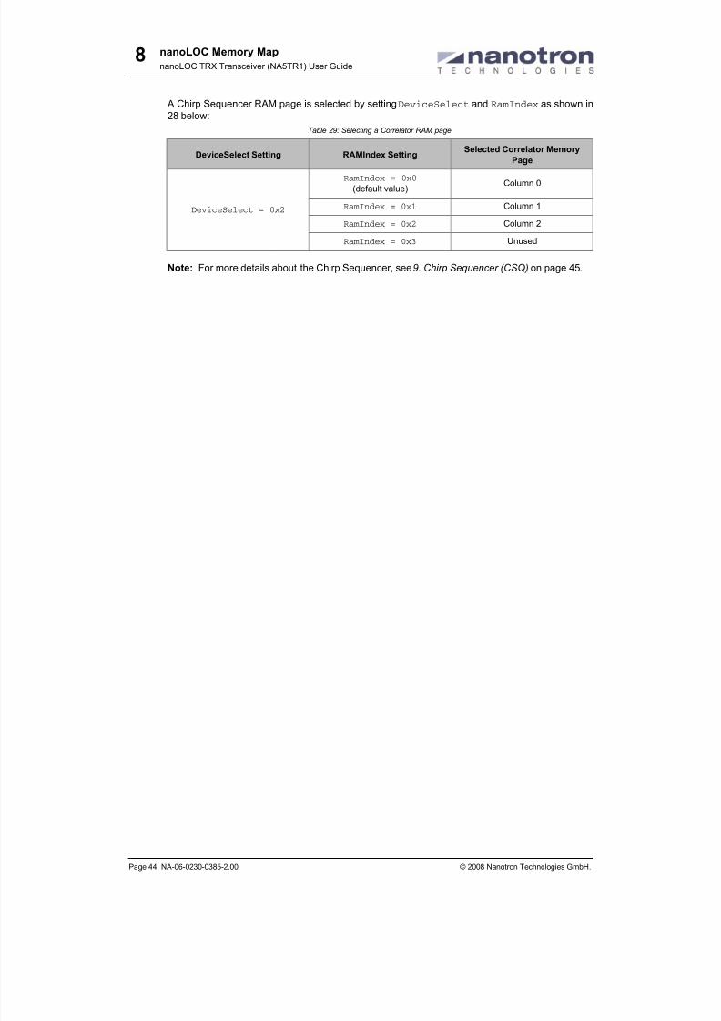
8/20/2019 nanoLOC NA5TR1 UserGuide
http://slidepdf.com/reader/full/nanoloc-na5tr1-userguide 60/325
nanoLOC Memory Map
nanoLOC TRX Transceiver (NA5TR1) User Guide
Page 44 NA-06-0230-0385-2.00 © 2008 Nanotron Technologies GmbH.
8
A Chirp Sequencer RAM page is selected by setting DeviceSelect and RamIndex as shown in
28 below:
Note: For more details about the Chirp Sequencer, see 9. Chirp Sequencer (CSQ) on page 45.
Table 29: Selecting a Correlator RAM page
DeviceSelect Setting RAMIndex SettingSelected Correlator Memory
Page
DeviceSelect = 0x2
RamIndex = 0x0
(default value)Column 0
RamIndex = 0x1 Column 1
RamIndex = 0x2 Column 2
RamIndex = 0x3 Unused
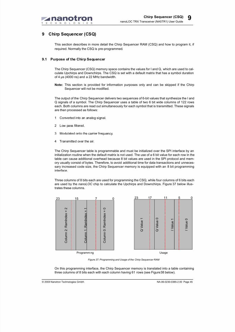
8/20/2019 nanoLOC NA5TR1 UserGuide
http://slidepdf.com/reader/full/nanoloc-na5tr1-userguide 61/325
Chirp Sequencer (CSQ)
nanoLOC TRX Transceiver (NA5TR1) User Guide
© 2008 Nanotron Technologies GmbH. NA-06-0230-0385-2.00 Page 45
9
9 Chirp Sequencer (CSQ)
This section describes in more detail the Chirp Sequencer RAM (CSQ) and how to program it, if
required. Normally the CSQ is pre-programmed.
9.1 Purpose of the Chirp Sequencer
The Chirp Sequencer (CSQ) memory space contains the values for I and Q, which are used to cal-
culate Upchirps and Downchirps. The CSQ is set with a default matrix that has a symbol duration
of 4 µs (4000 ns) and a 22 MHz bandwidth.
Note: This section is provided for information purposes only and can be skipped if the Chirp
Sequencer will not be modified.
The output of the Chirp Sequencer delivers two sequences of 6-bit values that synthesize the I and
Q signals of a symbol. The Chirp Sequencer uses a table of two 6 bit wide columns of 122 rows
each. Both columns are read out simultaneously for each symbol that is transmitted. These signalsare then processed as follows:
1 Converted into an analog signal.
2 Low pass filtered.
3 Modulated onto the carrier frequency.
4 Transmitted over the air.
The Chirp Sequencer table is programmable and must be initialized over the SPI interface by an
initialization routine when the default matrix is not used. The use of a 6 bit value for each row in the
table can cause additional overhead because 8 bit values are used in the SPI protocol and mem-ory usually consist of bytes. Therefore, to avoid additional time for data transactions and unneces-
sary increased code size, the Chirp Sequencer memory is equipped with an 8 bit programming
interface.
Three columns of 8 bits each are used for programming the CSQ, while four columns of 6 bits each
are used by the nanoLOC chip to calculate the Upchirps and Downchirps. Figure 37 below illus-
trates these columns.
Figure 37: Programming and Usage of the Chirp Sequencer RAM
On this programming interface, the Chirp Sequencer memory is translated into a table containing
three columns of 8 bits each with each column having 61 rows (see Figure 38 below).
C o l u m n 2 : R a m I n d e x =
2
C o
l u m n
1 :
R a m
I n d e x =
1
C o l u m n 0 : R a m I n d e x =
0
0723
Q V a l u e 1
Q V a l u e 0
I V a l u e 0
0523
I V a l u e 1
Programming Usage
111715

8/20/2019 nanoLOC NA5TR1 UserGuide
http://slidepdf.com/reader/full/nanoloc-na5tr1-userguide 62/325
Chirp Sequencer (CSQ)
nanoLOC TRX Transceiver (NA5TR1) User Guide
Page 46 NA-06-0230-0385-2.00 © 2008 Nanotron Technologies GmbH.
9
Figure 38: Chirp Sequencer programming interface format
Usually the I and Q sequences are given in two lists of 6 bit values. Before the data from both lists
can be written into the Chirp Sequencer memory, they must be formatted for the 8 bit programming
interface. This can be done prior to the compilation because the I and Q sequences are not com-
monly changed during the lifetime a software version.
9.2 Formatting the I and Q Values
The I and the Q values are formatted for the programming interface as follows:
1 Read in 122 elements of both lists (I and Q) into two separate arrays (I and Q array).
2 Allocate a two dimensional array of 3 columns by 61 rows.
3 Get the first and second I-value from the I-array.
4 Shift the second I-value 6 bits to the left, while discarding the upper 4 bits and merge it with the
first I-value to an 8 bit value.
5 Write this 8 bit value to the first row of the least significant column (byte 0) of the two dimen-
sional array.
6 Proceed this way (repeat steps 3 to 5) with the next I-values until the I-array is exhausted and
the byte-0-column is filled up.
7 Get the second I-value from the I-array and the first Q-value from the Q-array.
8 Shift the second I-value 2 bits to the right, while discarding the lower 2 bits, shift the first Q-
value 4 bits to the left, while discarding the higher 2 bits and merge both to an 8 bit value.
9 Write this 8 bit value to the first row of the middle column (byte 1) of the two dimensional array.
10 Proceed this way (repeat steps 7 to 9) with the next odd I-value and the next even Q-value until
both arrays are exhausted and the byte-1-column is filled up.
11 Get the first and second Q-value from the Q-array.
12 Shift the first Q-value 4 bits to the right while discarding the lower 4 bits, and then shift the sec-
ond Q-value 2 bits to the left and merge both to an 8 bit value.
13 Write this 8 bit value to the first row of the most significant column (byte 2) of the two dimen-
sional array.14 Proceed this way (repeat steps 11 to 13) with the next Q-values until the Q-array is exhausted
and the byte-2-column is filled up.
Q0
Q1
Q2
Q3
Q4
Q5
Q6
Q7
Q119
Q120
Q121
I0
I1
I2
I3
I4
I5
I6
I7
I120
I121
I0I1
I2I3
Q0Q1
Q2Q3
Q4Q5
Q6Q7
Q121 Q120
Q119
I4I5
I7
I121 I120
I6
8 bit8 bit8 bit 6 bit 6 bit
61
122
I/Q-Sequence-Format
Chirp Sequencer Programming Interface Format
Byte 2 Byte 1 Byte 0

8/20/2019 nanoLOC NA5TR1 UserGuide
http://slidepdf.com/reader/full/nanoloc-na5tr1-userguide 63/325
Chirp Sequencer (CSQ)
nanoLOC TRX Transceiver (NA5TR1) User Guide
© 2008 Nanotron Technologies GmbH. NA-06-0230-0385-2.00 Page 47
9
9.3 CSQ Writing Example
Note: Only first row of CSQ writing is depicted.
I1 = 11.1111b
I2 = 10.0111b
Q1 = 10.1000b
Q2 = 10.0001b
+ : Means operation or
4. I1 = 0011.1111b = 0011.1111b
I2 << 6 = 0010.0111b << 6 = 1100.0000b +
--------------------------------------------
row[0]column[0] = 1111.1111b
8. I2 >> 2 = 0010.0111b >> 2 = 0000.1001b
Q1 << 4 = 0010.1000b << 4 = 1000.0000b +
--------------------------------------------
row[0]column[1] = 1000.1000b
12. Q1 >> 4 = 0010.1000b >> 4 = 0000.0010b
Q2 << 2 = 0010.0001b << 2 = 1000.0100b +
--------------------------------------------
row[0]column[2] = 1000.0110b

8/20/2019 nanoLOC NA5TR1 UserGuide
http://slidepdf.com/reader/full/nanoloc-na5tr1-userguide 64/325
Chirp Sequencer (CSQ)
nanoLOC TRX Transceiver (NA5TR1) User Guide
Page 48 NA-06-0230-0385-2.00 © 2008 Nanotron Technologies GmbH.
9
Intentionally Left Blank

8/20/2019 nanoLOC NA5TR1 UserGuide
http://slidepdf.com/reader/full/nanoloc-na5tr1-userguide 65/325

8/20/2019 nanoLOC NA5TR1 UserGuide
http://slidepdf.com/reader/full/nanoloc-na5tr1-userguide 66/325
nanoLOC Packet and MACFrames
nanoLOC TRX Transceiver (NA5TR1) User Guide
Page 50 NA-06-0230-0385-2.00 © 2008 Nanotron Technologies GmbH.
10
The sequences of symbols in the Preamble should use following modulation system:
+ Upchirp/Downchirp – an alternating sequence of Upchirp/Downchirp pulses.
10.4 SyncWord Field
The SyncWord entity is a 64 bit code word derived from a 24-bit logical network ID (LNID) and is
used for frame synchronization.
Figure 41: SyncWord field
Different SyncWords can be used to facilitate frame synchronization on packets from different sta-
tions, networks, or logical channels. They are based on a (64,30) expurgated block code with the
PN-overlay 0x03848D96BBCC54FC to get good auto correlation properties. A Hamming distance
of 14 is guaranteed between SyncWords based on different LNIDs to allow frame synchronizationwith the presence of bit errors.
The following steps describe how the SyncWord is generated:
1 The information sequence is generated by appending 6 bits to the 24 bit LNID. If the MSB of
the LNID equals the value “0”, then the appended bits are 010101. If the MSB of the LNID is the
value “1”, then the appended bits are 101010.
2 The information sequence is pre-scrambled by XORing it with the bits 34 to 63 of the pseudo-
random noise (PN) sequence (0x03848D96BBCC54FC).
3 The parity bits are created through polynomial division of the information sequence by the gen-
erator polynomial 260534236651 (in octal notation). Parity bits are the rest of the division.
10.5 MACFrame Field
The contents of the MACFrame field defines the packet type. The size of the MACFrame can
range from 80 bits for an Ack packet to 114,996 bits for a Data packet using FEC. The MACFrame
field can consist of up to 10 fields depending on the packet type, as shown below.
Figure 42: MACFrame field
Note: FEC can be performed over all fields of the MACFrame.
The following provides a detailed description of all possible fields in a MACFrame entity.ScrInit (ScramblerInit) The ScramblerInit (ScrInit) field is used to initialize the bit scrambler at
the beginning of the receive cycle. The transmitter must set this field
Preamble SyncWord MACFrame Tail
64 bits
Preamble SyncWord MACFrame Tail
80 bit to 114,996 bits
Data
(1…MacDataLengthMax) *8 bits
CRC1
16 bits
FrameControl
3 bits
Length
13 bits
Address2
48 bits
Address1
48 bits
TypeCode
4 bits
Crypt
4 bits
ScInit
7 bits
CryptEn
1 bit
CryptId
2 bits
CryptSeqN
1 bit
CRC2
16 bitsor
32 bits
1bit
Packet body = 24 bits to 114,744 bitsPacket header = 144 bits= undefined

8/20/2019 nanoLOC NA5TR1 UserGuide
http://slidepdf.com/reader/full/nanoloc-na5tr1-userguide 67/325
nanoLOC Packet and MACFrames
nanoLOC TRX Transceiver (NA5TR1) User Guide
© 2008 Nanotron Technologies GmbH. NA-06-0230-0385-2.00 Page 51
10
with the initial value of the scrambler since this value is not known at
the receiver. This value can be changed for every packet.
The receiver uses the ScramblerInit value for descrambling the MAC-
Frame. Scrambling is performed over all fields of the MACFrame
(except the ScramblerInit field) to randomize the data using highlyredundant patterns so that the probability of large zero patterns is
minimized.
Crypt (EncryptionControl) The EncryptionControl (Crypt) field is 4 bits in length and consists of
the encryption enable switch (CryptEn), the encryption ID (CryptID),
and the sequential numbering scheme (CryptSeqN) for encryption.
The CryptEn bit is used to indicate that encryption is used.
The 2 bit CryptID field, which is used for encrypted Data, Brdcast and
TimeB packets, selects one of four secret keys (CryptKey, Crypt-
Clock) which are found in page one of RAM.
The CryptSeqN bit, which always starts with zero, increments Crypt-Clock if the current CryptSeqN bit is unequal to the previous bit.
TypeCode The TypeCode field is 4 bits in length. It identifies the packet type.
Possible values include Data, Ack, Brdcast, TimeB, Req2S, and
Clr2S.
A device that receives a frame with an invalid TypeCode will discard
the packet without indication to the sending station or to the LLC.
Address1 The Address1 field is 48 bits in length and contains the destination
address in all packet types, with the exception of the TimeB packet
where the Address1 field contains a Real Time Clock value.
Address2 The Address2 field is 48 bits in length and contains the source
address in Data, Brdcast, TimeB and Req2S packet types.
Length The Length field is 13 bits in length and specifies the number of bytes
of the Data field. It exists only in the Data, Brdcast, TimeB, Req2S and
Clr2S packet types.
All bits set to “0” indicate a Data field of 8192 bytes. The maximum
Length value allowed in a subset of this specification is defined by the
MacDataLengthMax attribute. A station receiving a MACFrame with a
value greater than the MacDataLengthMax (Data packet) or the
MacBrdCastLengthMax (Brdcast packet) discards the packet without
indication to the sender or to the LLC.
Note: MacDataLengthMax and MacBrdCastLengthMax are defined in
Appendix 1: Attributes and Constants on page 289.
FrameControl The FrameControl field is 3 bits in length and is transparent for the
nanoLOC chip. For TX, these bits are loaded from RAM together with
the TxLength field and sent in the MACFrame. For RX, these bits are
stored in RAM together with the RxLength field received in the MAC-
Frame where they can be read and used by an application.
In several applications the FrameControl field is used on the software
level to implement functionalities such as Link Control Channel
(where the third bit is defined as a logical channel bit LCh), a sequen-
tial numbering scheme (where the second bit is defined as a
sequence numbering bit SeqN), and/or a packet fragmentationscheme (where the first bit is defined as a fragmentation control bit
FragC). These bits are as shown below.

8/20/2019 nanoLOC NA5TR1 UserGuide
http://slidepdf.com/reader/full/nanoloc-na5tr1-userguide 68/325
nanoLOC Packet and MACFrames
nanoLOC TRX Transceiver (NA5TR1) User Guide
Page 52 NA-06-0230-0385-2.00 © 2008 Nanotron Technologies GmbH.
10
Figure 43: FrameControl field used for Network Protocol
CRC1 The CRC1 field is 16 bits in length and performs a Cyclic Redundancy
Check over the MACFrame header information. The CRC1 allows a
checking of the integrity of the protocol information (such as
addresses and length) in the MACFrame so that the MACFrame
header information is immediately verified and is independent of the
CRC mode of the data packet.
The CRC1 is calculated on the following MACFrame fields: Encryp-
tionControl, TypeCode, Address1, Address2, and Length.
Data The Data field is a variable length field that contains the data for the
logical channels. It exists only in the Data and Brdcast packets. The
Length field specifies the length in bytes of the Data field.
The minimum length is one byte. The maximum length is defined by
the MacDataLengthMax and MacBrdcastLengthMax attributes, which
is 8192 bytes.
Note: MacDataLengthMax and MacBrdCastLengthMax are defined in
Appendix 1: Attributes and Constants on page 289.
CRC2 The CRC2 field is 16 or 32 bits in length and performs a cyclic redun-
dancy check on the Data field of Data and Brdcast packets. Different
polynomials of 16 or 32 bit lengths are defined and can be selected.
10.5.1 MACFrame of a Data Packet
The MACFrame of a Data packet contains up to 8192 data bytes. A Data packet MACFrame is
shown below.
Figure 44: MACFrame format of Data packet
The following fields have information that is specific to the Data packet:
TypeCode Contains the type code of the Data packet.
Address1 Contains the destination address (DestinationAddress).
Address2 Contains the source address (SourceAddress).
Length Contains the length of the Data packet in bytes.
FrameControl These bits are transparent to the nanoLOC chip. They are used in
nanoLOC Ranging Application Software, as follows:
Table 1: Ranging Data Packets
Ranging Data Packet Type Value
Normal Data Packet 0x00
Ranging_Start Packet 0x01
FragC
1 bit
FrameControl
3 bits
SeqN
1 bit
LCh
1 bit
Data
(1…MacDataLengthMax) * 8bits
CRC1
16 bits
FrameControl
3 bits
Length
13 bits
Address2
48 bits
Address1
48 bits
TypeCode
4 bits
Crypt
4 bits
ScInit
7 bits
CRC2
16 or32 bits
1bit
= undefined

8/20/2019 nanoLOC NA5TR1 UserGuide
http://slidepdf.com/reader/full/nanoloc-na5tr1-userguide 69/325
nanoLOC Packet and MACFrames
nanoLOC TRX Transceiver (NA5TR1) User Guide
© 2008 Nanotron Technologies GmbH. NA-06-0230-0385-2.00 Page 53
10
Note: FragC bit (bit 1) = LSB. LCh bit (bit 3) = MSB.
Data The maximum length of the Data field used in an implementation sub-
set of this specification is defined by the MacDataLengthMax attribute.
If messages with more than MacDataLengthMax bytes have to be
transmitted, they can be fragmented into several Data packets of dif-
ferent lengths. If a Data packet is received with more than MACDataL-
enghtMax bytes, it is discarded without indication to the sender or to
the LLC.
Note: MacDataLengthMax is defined in Appendix 1: Attributes and
Constants on page 289.
10.5.2 MACFrame of an Acknowledgement (Ack) Packet
An Ack packet is sent by the receiver to acknowledge the successful reception of a Data packet.
The MACFrame of an Ack packet is shown below.
Figure 45: MACFrame format of an Ack packet
The following fields have information that is specific to the Ack packet:
TypeCode Contains the type code of the Ack packet.
Address1 Contains the destination address (DestinationAddress).
10.5.3 MACFrame of a Broadcast (Brdcast) Packet
A Brdcast packet is sent by a station to give specific information to either all stations in range (a
broadcast message) or only a group of stations in range (a multicast message). The MACFrame of
a Brdcast packet is shown below.
Figure 46: MACFrame format of a Brdcast packet
The following fields have information that is specific to the Brdcast packet:
FrameControl Since a Brdcast packet is sent as a broadcast to more than one sta-
tion, it must not be acknowledged by any station receiving the packet.
Because of the lack of retransmission possibilities for Brdcast packets
(unacknowledged transmission) fragmentation is impossible. There-
fore, the FragC and SeqN bits must be set to the value “0”.Data The maximum length of the Data field used in a implementation sub-
set of this specification is defined by MacBrdCastLengthMax attribute.
Ranging_Answer1 Packet 0x02
Ranging_Answer2 Packet 0x03Ranging_Fast_Start Packet 0x04
Ranging_Fast_Answer1 0x05
Table 1: Ranging Data Packets
Ranging Data Packet Type Value
CRC1
16 bits
Address1
48 bits
TypeCode
4 bits
0x0
4 bits
ScInit
7 bits1bit
= undefined
Data
(1…MacDataLengthMax) * 8bits
CRC1
16 bits
FrameControl
3 bits
Length
13 bits
Address2
48 bits
Address1
48 bits
TypeCode
4 bits
Crypt
4 bits
ScInit
7 bits
CRC2
16 bitsor
32 bits
1bit
= undefined

8/20/2019 nanoLOC NA5TR1 UserGuide
http://slidepdf.com/reader/full/nanoloc-na5tr1-userguide 70/325

8/20/2019 nanoLOC NA5TR1 UserGuide
http://slidepdf.com/reader/full/nanoloc-na5tr1-userguide 71/325
nanoLOC Packet and MACFrames
nanoLOC TRX Transceiver (NA5TR1) User Guide
© 2008 Nanotron Technologies GmbH. NA-06-0230-0385-2.00 Page 55
10
The following fields have information that is specific to the Req2S packet:
Length The Length field indicates the length of the Data packet (in bytes) of
the requested transmission.
TypeCode Type code of the Req2S packet.
Address1 Contains the destination address (DestinationAddress).
Address2 Contains the source address (SourceAddress).
FrameControl These fields are undefined.
10.5.6 Clear to Send (Clr2S) Packet MACFrame
The Clr2S packet confirms a requested frame transmission of a station through a Req2S packet,
indicating that a Data packet can be transmitted. The Addess2 and Length fields are copied from
the Req2S packet and sent back to the requesting station. A Clr2S packet MACFrame is shown
below.
Figure 49: MACFrame format of Clr2S packet
The following fields have information that is specific to the Clr2s packet:
TypeCode Contains the type code of the Clr2s packet.
Address1 Contains the destination address (DestinationAddress).
Length Contains the length of the packet in bytes.
FrameControl These fields are undefined.
10.6 Tail Field
The Tail field is used as a delimiter between the end of a packet. Tail symbols are required in on-
off-keying systems for the physical carrier sensing mechanism. For instance, consecutive off-sym-
bols at the end of a packet and the following interframe space interval could be misinterpreted by
stations trying to access the media as a physically idle medium.
Figure 50: Tail field
The Tail is a fixed-length sequence of MacTailSymbols (4) bits defined below for the modulation
systems:
+ Upchirp/Downchirp – an alternating sequence of Upchirp and Downchirp pulses.
+ Upchirp/Off – a continuous sequence of Upchirp pulses.
+ Downchirp/Off – a continuous sequence of Downchirp pulses.
CRC1
16 bits
0b000
3 bits
Length
13 bits
Address1
48 bits
TypeCode
4 bits
0x0
4 bits
ScInit
7 bits1bit
= undefined
Preamble SyncWord MACFrame Tail
MACTailSymbols

8/20/2019 nanoLOC NA5TR1 UserGuide
http://slidepdf.com/reader/full/nanoloc-na5tr1-userguide 72/325
nanoLOC Packet and MACFrames
nanoLOC TRX Transceiver (NA5TR1) User Guide
Page 56 NA-06-0230-0385-2.00 © 2008 Nanotron Technologies GmbH.
10
Intentionally Left Blank

8/20/2019 nanoLOC NA5TR1 UserGuide
http://slidepdf.com/reader/full/nanoloc-na5tr1-userguide 73/325
Frame Control Scheme
nanoLOC TRX Transceiver (NA5TR1) User Guide
© 2008 Nanotron Technologies GmbH. NA-06-0230-0385-2.00 Page 57
11
11 Frame Control Scheme
This section describes a frame control scheme that can be implemented in software. This schemes
use the FrameControl field of the MACFrame, which is transparent to the nanoLOC chip.
11.1 Logical Channels
The Link Control Manger should be implemented in the Data Link Layer. The following describes
the settings of the LCh bit in the FrameControl field which selects between the Link Control Chan-
nel and the User Data Channel.
11.1.1 Link Control Channel
The LCh bit is used to distinguish between the two logical channels (LCCh and UDCh). A value “0”
indicates the user data channel (UDCh) while a value “1” indicates the link control channel (LCCh).
The Link Control Channel (LCCh) carries control information that is exchanged between the Link
Control Managers (LCM) of two stations. The LCCh is indicated by the Logical Channel bit (LCh)
set to the value “1” in the FrameControl field of Data or Brdcast packets.
Figure 51: LCh field set ti LCCh
Information exchanged between two stations via the Link Control Channel is shown below.
Figure 52: Link Control Channel
Note: For more details, see 11.2. Link Control Management on page 58.
11.1.2 User Data Channel
The User Data Channel (UDCh) carries user data that is exchanged between the Data Link Con-trols (DLC) of two stations. The UDCh channel is indicated by the Logical Channel bit (LCh) set to
the value “0” in the FrameControl field of Data or Broadcast packets.
LCh = 1FragC
1 bit
Data
(1…MacDataLengthMax) * 8bits
CRC1
16 bits
FrameControl
3 bits
Length
13 bits
Address2
48 bits
Address1
48 bits
TypeCode
4 bits
Crypt
4 bits
ScInit
7 bits
SeqN
1 bit 1 bit
CRC2
16 bitsor
32 bits
1bit
= undefined
LCCh
-01 Transceiver Chip
DLL
Physical Layer (PHY)
Media Access Layer (MAC)
Link Control Manager(LCM)
Data Link Layer
-01 Transceiver ChipPhysical Layer (PHY)
Media Access Layer (MAC)
Link Control Manager
(LCM)
Data Link Layer
Station one Station two

8/20/2019 nanoLOC NA5TR1 UserGuide
http://slidepdf.com/reader/full/nanoloc-na5tr1-userguide 74/325
Frame Control Scheme
nanoLOC TRX Transceiver (NA5TR1) User Guide
Page 58 NA-06-0230-0385-2.00 © 2008 Nanotron Technologies GmbH.
11
Figure 53: LCh field set to UDCh
Information exchanged between two stations via the User Data Channel is shown below.
Figure 54: User Data Channel
11.2 Link Control Management
Link Control Management Protocol (LCMP) messages are used for link set-up, security, and con-
trol. They are transferred in the Data field instead of user data and are indicated by a bit with the
value “1” in the LCh of the FrameControl field. The messages are filtered out and interpreted by the
Link Control Management (LCM) on the receiving side and are not propagated to higher layers.
LCMP messages have higher priority than user data. This means that if the LCM needs to send a
message, it is not delayed by user data traffic, although it can be delayed by many retransmissions
of individual packets.
LCh = 0FragC
1 bit
Data
(1…MacDataLengthMax) * 8bits
CRC1
16 bits
FrameControl
3 bits
Length
13 bits
Address2
48 bits
Address1
48 bits
TypeCode
4 bits
Crypt
4 bits
ScInit
7 bits
SeqN
1 bit 1 bit
CRC2
16 bitsor
32 bits
1bit
= undefined
UDCh
-01 Transceiver Chip
DLL
Physical Layer (PHY)
Media Access Layer (MAC)
Link Control Manager(LCM)
Data Link Layer
-01 Transceiver ChipPhysical Layer (PHY)
Media Access Layer (MAC)
Link Control Manager(LCM)
Data Link Layer
Station one Station two
DLL Data DLL Data

8/20/2019 nanoLOC NA5TR1 UserGuide
http://slidepdf.com/reader/full/nanoloc-na5tr1-userguide 75/325
MACFrame Configuration (Auto/Transparent)
nanoLOC TRX Transceiver (NA5TR1) User Guide
© 2008 Nanotron Technologies GmbH. NA-06-0230-0385-2.00 Page 59
12
12 MACFrame Configuration (Auto/Transparent)
This section explains how to configure the MACFrame in Auto and Transparent mode.
12.1 Overview
A transmitted or received packet contains a Preamble, a SyncWord, the MACFrame, and a Tail,
which are used by the nanoLOC chip to help process the received packet. The MACFrame, how-
ever, contains the raw data which is used by upper layers.
Figure 55: MACFrame contents
The nanoLOC TRX Transceiver provides a wide range of features that can be automatically set in
the MACFrame as it is prepared for transmission, or read out when a MACFrame is received.
These include Forward Error Correction, Encryption, Address Matching, and so on. However, the
chip provides the option of allowing software to configure the MACFrame. These two modes are
Auto Mode and Transparent Mode:
+ In Auto mode, for TX, the MACFrame is configured by automatically by hardware (the
nanoLOC chip) using data provided in chip register settings and buffers, while for RX, the hard-
ware (the nanoLOC chip) parses the received MACFrame and stores the resultant values in
chip registers and buffers for further use by software.
+ In Transparent mode, for TX, software configures and prepares the MACFrame and stores in in
a buffer for transmission, while for RX, the MACFrame is “transparent” to the chip and stores
the entire MACFrame in a buffer for further use by software.
12.2 Field for Setting MACFrame Auto and Transparent Mode
The following field is used for setting MACFrame Auto and Transparent Mode.
12.3 MACFrame Auto Mode
When the nanoLOC chip is set to Auto Mode, the MAC header values and data payload used for
TX and RX are stored in a single buffer which has been divided into an upper and a lower part. The
upper half stores MAC header data while the lower half stores the packet payload.
Figure 56: Auto mode
For TX, the digital part of the chip builds the MAC header using values stored in chip buffers andregisters, including the payload data. Additional packet requirements (Preamble, SyncWord and
Tail) are added to this completed MACFrame and the packet is transmitted.
DataCRC1FrameControl
Length Address2 Address1TypeCode
CryptScInit CRC2
= undefined
Preamble SyncWord MACFrame Tail
Table 32: Wake-up time fields
Field Offset Read/Write Description
TxRxBbBufferMode0 0x4A
WO
brst
BbClk
Sets the TX and RX data as either two segments
(Auto) or all four segments (Transparent).
MAC Header
Payload
Baseband RAM buffer
Upper half
Lower half

8/20/2019 nanoLOC NA5TR1 UserGuide
http://slidepdf.com/reader/full/nanoloc-na5tr1-userguide 76/325
MACFrame Configuration (Auto/Transparent)
nanoLOC TRX Transceiver (NA5TR1) User Guide
Page 60 NA-06-0230-0385-2.00 © 2008 Nanotron Technologies GmbH.
12
For RX, the Preamble, SyncWord and Tail are removed and the MAC header and payload of
extracted MACFrame are stored in chip registers and buffers. Software can then read out the
resultant MAC header values and payload data.
12.3.1 Setting MACFrame Auto Mode (Default)
To set MACFrame Auto mode, do the following:
+ Set TxRxBbBufferMode0 = 0x0
where, 0x0 = NA_TxRxBufferMode0Auto_BC_C
Note: Auto mode is the default setting (0x0)
12.4 MACFrame Transparent Mode
When the nanoLOC chip is set to Transparent Mode, MAC header values and data payload are
prepared in software and a complete MACFrame must be provided to the chip. A single buffer is
used to store the MACFrame, where both the upper half and the lower half are available for storing
the complete MACFrame.
Figure 57: Transparent mode
For TX, software builds the MACFrame by assembling the MAC header and payload data. This
assembled MACFrame is placed in the a baseband RAM buffer(s). The nanoLOC chip builds the
packet by using this MACFrame and additional packet requirements (Preamble, SyncWord and
Tail) after which the packet is transmitted.
For RX, the Preamble, SyncWord and Tail are removed and the MACFrame is extracted from thepacket and stored in the baseband RAM buffer. This MACFrame is read out and provided to an
application for further processing.
12.4.1 Setting MACFrame Transparent Mode
To set Transparent mode for the MACFrame, do the following:
+ Set TxRxBbBufferMode0 = 0x1
where 0x1 = NA_TxRxBufferMode0Transparent_BC_C
Payload
Payload
Baseband RAM buffer
Upper half
Lower half

8/20/2019 nanoLOC NA5TR1 UserGuide
http://slidepdf.com/reader/full/nanoloc-na5tr1-userguide 77/325
Baseband RAM Configuration
nanoLOC TRX Transceiver (NA5TR1) User Guide
© 2008 Nanotron Technologies GmbH. NA-06-0230-0385-2.00 Page 61
13
13 Baseband RAM Configuration
This section describes the four possible configurations of the baseband RAM using the TX/RX
buffer and MACFrame modes, which are Auto/Duplex, Auto/Simplex, Transparent/Duplex, and
Transparent/Simplex.
13.1 Overview
The 1024 byte memory space of the nanoLOC chip consists of four baseband RAM segments
totaling 512 bytes.
Note: See also 8. nanoLOC Memory Map on page 39.
Each of the four segments has a 128 byte register space, three of which are mappings of the chip
register space (0x00 to 0x7F). The mappings of the register space and the four baseband RAM
segments are shown in the following figure.
Figure 58: Baseband RAM memory space
13.1.1 Configurable Spaces
The chip register memory space is non-configurable. Values written to the register address spaces
(0x00 - 0x7F, 0x100 - 0x17F, 0x200 - 0x27F and 0x300 - 0x37F) always access the same Register
Block (e.g. 0x00 is equivalent to 0x100, 0x200 and 0x300).
Baseband RAM, however, is configurable. Pages 0 to 3 of the Baseband RAM is configurable to
one of four mode combinations, as described in table 33 below.
Table 33: Baseband RAM configuration modes
Mode Description
Auto/Duplex ModeTwo separate data buffers of 128 bytes each of the baseband RAM are
used (Page 2 and Page 3).
Auto/Simplex ModeTwo baseband RAM pages of 128 bytes each are combined for a sin-
gle data buffer for both RX and TX (Page 2 and Page 3)
Transparent/DuplexTwo separate buffers of 256 bytes each are used for an RX data buffer
and a TX data buffer (Page 0, Page 1, Page 2 and Page 3).
Transparent/Simplexa single 512 byte RX/TX data buffer is used sequentially for either a RX
data buffer or TX data buffer (Page 0, Page 1, Page 2 and Page 3).
Baseband RAM Page 3
Register
128 bytes
0x300
0x37F0x380
0x3FF
128 bytes
Baseband RAM Page 2
Register
128 bytes
0x200
0x27F0280
0x2FF
128 bytes
Baseband RAM Page 1
Register
128 bytes
0x100
0x17F0x180
0x1FF
128 bytes
Baseband RAM Page 0
Register
128 bytes
0x00
0x7F0x080
0x0FF
128 bytes
≅
Page 0
Page 1
Page 2
Page 3
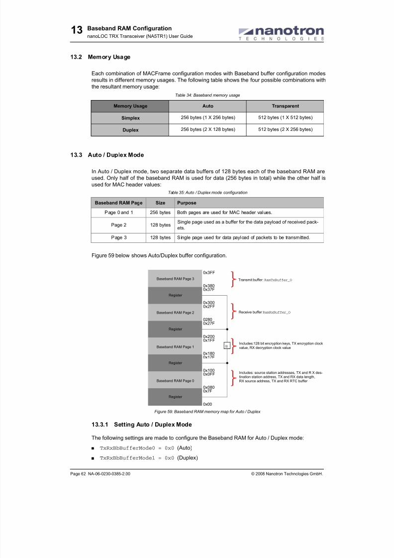
8/20/2019 nanoLOC NA5TR1 UserGuide
http://slidepdf.com/reader/full/nanoloc-na5tr1-userguide 78/325
Baseband RAM Configuration
nanoLOC TRX Transceiver (NA5TR1) User Guide
Page 62 NA-06-0230-0385-2.00 © 2008 Nanotron Technologies GmbH.
13
13.2 Memory Usage
Each combination of MACFrame configuration modes with Baseband buffer configuration modes
results in different memory usages. The following table shows the four possible combinations with
the resultant memory usage:
13.3 Auto / Duplex Mode
In Auto / Duplex mode, two separate data buffers of 128 bytes each of the baseband RAM are
used. Only half of the baseband RAM is used for data (256 bytes in total) while the other half isused for MAC header values:
Figure 59 below shows Auto/Duplex buffer configuration.
Figure 59: Baseband RAM memory map for Auto / Duplex
13.3.1 Setting Auto / Duplex Mode
The following settings are made to configure the Baseband RAM for Auto / Duplex mode:
+ TxRxBbBufferMode0 = 0x0 (Auto)
+ TxRxBbBufferMode1 = 0x0 (Duplex)
Table 34: Baseband memory usage
Memory Usage Auto Transparent
Simplex 256 bytes (1 X 256 bytes) 512 bytes (1 X 512 bytes)
Duplex 256 bytes (2 X 128 bytes) 512 bytes (2 X 256 bytes)
Table 35: Auto / Duplex mode configuration
Baseband RAM Page Size Purpose
Page 0 and 1 256 bytes Both pages are used for MAC header values.
Page 2 128 bytesSingle page used as a buffer for the data payload of received pack-
ets.
Page 3 128 bytes Single page used for data payload of packets to be transmitted.
0x300
0x37F0x380
0x3FF
0x200
0x27F0280
0x2FF
0x100
0x17F0x180
0x1FF
0x00
0x7F0x080
0x0FF
≅
Transmit buffer: RamTxBuffer_O
Receive buffer RamRxBuffer_O
Includes: source station addresses, TX and R X des-tination station address, TX and RX data length,RX source address, TX and RX RTC buffer
Includes:128 bit encryption keys, TX encryption clock
value, RX decryption clock value
Baseband RAM Page 3
Register
Baseband RAM Page 2
Register
Baseband RAM Page 1
Register
Baseband RAM Page 0
Register

8/20/2019 nanoLOC NA5TR1 UserGuide
http://slidepdf.com/reader/full/nanoloc-na5tr1-userguide 79/325
Baseband RAM Configuration
nanoLOC TRX Transceiver (NA5TR1) User Guide
© 2008 Nanotron Technologies GmbH. NA-06-0230-0385-2.00 Page 63
13
13.3.2 Start Addresses of the RX/TX Data Buffers
The RX data buffer (set by RamRxBuffer_O) consists of two blocks of 64 bytes each, where:
+ Start address of lower block for RX = RamRxBuffer_0
+ Start address of upper block for RX = RamRxBuffer_0 + 0x040
The TX data buffer (set by RamTxBuffer_O) consists of two blocks of 64 bytes each, where:
+ Start address of lower block for TX = RamTxBuffer_0
+ Start address for upper block for TX = RamTxBuffer_0 + 0x040
Note: See also Buffer Access Synchronization on page 73.
13.4 Auto / Simplex Mode
In Auto / Simplex mode, two baseband RAM pages of 128 bytes each are combined for a singledata buffer for both RX and TX. Only half of the baseband RAM is used for data (256 bytes in total)
while the other half is used for MAC header values:
Figure 60 shows a memory map of Auto/Simplex buffer configuration.
Figure 60: Baseband RAM memory map for Auto / Duplex
13.4.1 Setting Auto / Simplex Mode
The following settings are made to configure the Baseband RAM for Auto / Simplex mode:
+ TxRxBbBufferMode0 = 0x0 (Auto)
+ TxRxBbBufferMode1 = 0x1 (Simplex)
Table 36: Auto / Simplex mode configuration
Baseband RAM Page Size Purpose
Page 0 and 1 256 bytes Both pages are used for MAC header values.
Page 2 and 3 256 bytesBoth pages are used as a data buffer for the data payload of
received packets or packets to be transmitted.
0x300
0x37F0x380
0x3FF
0x200
0x27F0280
0x2FF
0x100
0x17F0x180
0x1FF
0x00
0x7F0x080
0x0FF
≅
TX/RX Data Buffer: RamTxRxBuffer_0
Includes: source station addresses, TX and R X des-tination station address, TX and RX data length,RX source address, TX and RX RTC buffer
Includes: 128 bit encryption keys, TX encryptionclock value, RX decryption clock value
Baseband RAM Page 3
Register
Baseband RAM Page 2
Register
Baseband RAM Page 1
Register
Baseband RAM Page 0
Register

8/20/2019 nanoLOC NA5TR1 UserGuide
http://slidepdf.com/reader/full/nanoloc-na5tr1-userguide 80/325
Baseband RAM Configuration
nanoLOC TRX Transceiver (NA5TR1) User Guide
Page 64 NA-06-0230-0385-2.00 © 2008 Nanotron Technologies GmbH.
13
13.4.2 Start Addresses of the RX/TX Data Buffer
The TX / RX data buffer (set by RamTxRxBuffer_0) consists of two blocks of 128 bytes each,
where:
+
Start address of lower block for RX and TX = RamTxRxBuffer_0
+ Start address of upper block for RX and TX = RamTxRxBuffer_0 + 0x100
Note: See also 17. Buffer Access Synchronization on page 73.
13.5 Transparent / Duplex Mode
In Transparent / Duplex mode, two separate buffers of 256 bytes each are used for an RX data
buffer and a TX data buffer. Software is responsible for configuring and reading the MACFrame,
including MAC header values and data payload.
Figure 61 below shows the memory map of Transparent/Duplex buffer configuration.
Figure 61: Baseband RAM memory map for Auto / Duplex
13.5.1 Setting Transparent / Duplex Mode
The following settings are made to configure the baseband RAM for Transparent / Duplex mode:
+ TxRxBbBufferMode0 = 0x1 (Transparent)
+ TxRxBbBufferMode1 = 0x0 (Duplex)
13.5.2 Start Addresses of the RX/TX Data Buffers
The RX data buffer (set by RamRxTransBuffer_0) consists of two blocks of 128 bytes each,
where:
+ Start address of lower block for RX = RamRxTransBuffer_0
+ Start address of upper block for RX = RamRxTransBuffer_0 + 0x100
Table 37: Transparent / Duplex mode configuration
Baseband RAM Page Size Purpose
Page 0 and 1 256 bytes Both pages are used as a data buffer for received packets.
Page 2 and 3 256 bytes Both pages are used as a data buffer for packets to be transmitted.
0x300
0x37F0x380
0x3FF
0x200
0x27F0280
0x2FF
0x100
0x17F0x180
0x1FF
0x00
0x7F0x080
0x0FF
≅
TX Data Buffer: RamTxTransBuffer_0
RX Data Buffer: RamRxTransBuffer_0
Baseband RAM Page 3
Register
Baseband RAM Page 2
Register
Baseband RAM Page 1
Register
Baseband RAM Page 0
Register

8/20/2019 nanoLOC NA5TR1 UserGuide
http://slidepdf.com/reader/full/nanoloc-na5tr1-userguide 81/325
Baseband RAM Configuration
nanoLOC TRX Transceiver (NA5TR1) User Guide
© 2008 Nanotron Technologies GmbH. NA-06-0230-0385-2.00 Page 65
13
The TX data buffer (set by RamTxTransBuffer_0) consists of two blocks of 128 bytes each,
where
+ Start address of lower block for TX = RamTxTransBuffer_0
+ Start address of upper block for TX = RamTxTransBuffer_0 + 0x100
Note: See also Buffer Access Synchronization on page 73.
13.6 Transparent / Simplex Mode
In this configuration, a single 512 byte RX/TX data buffer is used sequentially for either a RX data
buffer or TX data buffer. It consists of the complete baseband RAM memory space of four 128 byte
buffers. Software is responsible for configuring and reading the MACFrame, including MAC header
values and data payload.
Figure 62 below shows the memory map of Transparent/Simplex buffer configuration.
Figure 62: Baseband RAM memory map for Auto / Duplex
13.6.1 Setting Transparent / Simplex Mode
The following settings are made to configure the baseband RAM for Transparent/Simplex mode:
+ TxRxBbBufferMode0 = 0x1 (Transparent)
+ TxRxBbBufferMode1 = 0x1 (Simplex)
13.6.2 Start Addresses of the RX/TX Data Buffer
The RX/TX data buffer (set by RamRxTransBuffer_0) consists of two blocks of 256 bytes each,
where:
+ For the lower block:
+ Start address of lower half = RamTxRxTransBuffer_0
+ Start address of upper half = RamTxRxTransBuffer_0 + 0x100
Table 38: Transparent / Simplex mode configuration
Baseband RAM Page Size Purpose
Page 0, 1, 2, and 3 256 bytes All pages are used as a single data buffer for either received packetsor packets to be transmitted.
0x300
0x37F0x380
0x3FF
0x200
0x27F0280
0x2FF
0x100
0x17F0x180
0x1FF
0x00
0x7F0x080
0x0FF
≅
RX/TX Data Buffer: RamTxRxTransBuffer
Baseband RAM Page 3
Register
Baseband RAM Page 2
Register
Baseband RAM Page 1
Register
Baseband RAM Page 0
Register

8/20/2019 nanoLOC NA5TR1 UserGuide
http://slidepdf.com/reader/full/nanoloc-na5tr1-userguide 82/325
Baseband RAM Configuration
nanoLOC TRX Transceiver (NA5TR1) User Guide
Page 66 NA-06-0230-0385-2.00 © 2008 Nanotron Technologies GmbH.
13
+ For the upper block:
+ Start address of lower half = RamTxRxTransBuffer_0 + 0x200
+ Start address of upper half = RamTxRxTransBuffer_0 + 0x300
Note: See also 17. Buffer Access Synchronization on page 73.
Warnings: It is important to be aware that each of the two blocks are spread over two segments.

8/20/2019 nanoLOC NA5TR1 UserGuide
http://slidepdf.com/reader/full/nanoloc-na5tr1-userguide 83/325
Buffer Configuration (Simplex/Duplex)
nanoLOC TRX Transceiver (NA5TR1) User Guide
© 2008 Nanotron Technologies GmbH. NA-06-0230-0385-2.00 Page 67
14
14 Buffer Configuration (Simplex/Duplex)
This section describes how to configure the TX and RX buffers in Duplex and Simplex mode.
14.1 Overview
The nanoLOC chip can process packets for transmit and receive sequentially or simultaneously. In
sequential mode or Simplex Mode, at any given time the chip can process either received packets
or packets for transmission. In simultaneous mode or Duplex Mode, at any given time, the chip can
process both received packets and packets for transmission. Each mode requires a configuration
of the baseband RAM.
14.2 Field for Setting Duplex and Simplex Mode
The following field is used for setting Duplex or Simplex mode for the baseband TX/RX buffer
14.3 Duplex Mode (Default)
In Duplex Mode, the baseband RAM buffer is split into two blocks, one for TX and one for RX. The
TX and RX buffer operations are independent of each other. However, to allow simultaneous TX
and RX buffer operations, smaller buffers are available for MACFrame data (MAC headers and
data payload). The size of these blocks are dependent on the MACFrame mode (Auto or Transpar-
ent). Duplex Mode is the default setting.
Figure 63: Baseband buffer in Duplex mode
Note: See 12. MACFrame Configuration (Auto/Transparent) on page 59.
14.3.1 Configuring the Baseband RAM for Duplex Mode
To set the baseband RAM for Duplex Mode, do the following:
+ Set TxRxBbBufferMode1 = 0x0
where 0x0 = NA_TxRxBufferMode1Duplex_BC_C.
14.4 Simplex Mode
In Simplex Mode, a single baseband RAM buffer of at least two pages is used for both TX and RX.
This results in a larger buffer available for the MACFrames. The size of the buffer is dependent on
the selection of MACFrame mode (Auto or Transparent).
Figure 64: Baseband buffer in Simplex mode
Note: See 12. MACFrame Configuration (Auto/Transparent) on page 59.
Table 39: Wake-up time fields
Field Offset Read/Write Description
TxRxBbBufferMode1 0x4A
WO
brst
BbClk
Sets the data buffer for TX and RX as either two
blocks (Duplex) or a single block (Simplex).
TX Buffer
RX Buffer
Baseband RAM buffer
First block
Second block
Both blocks used as asingle buffer
Baseband RAM buffer
TX Buffer
RX Buffer

8/20/2019 nanoLOC NA5TR1 UserGuide
http://slidepdf.com/reader/full/nanoloc-na5tr1-userguide 84/325
Buffer Configuration (Simplex/Duplex)
nanoLOC TRX Transceiver (NA5TR1) User Guide
Page 68 NA-06-0230-0385-2.00 © 2008 Nanotron Technologies GmbH.
14
14.4.1 Configuring the Baseband RAM for Simplex Mode
To set the baseband RAM for Simplex Mode, do the following:
+ Set TxRxBbBufferMode1 = 0x1
where 0x1 = NA_TxRxBufferMode1Simpex_BC_C.
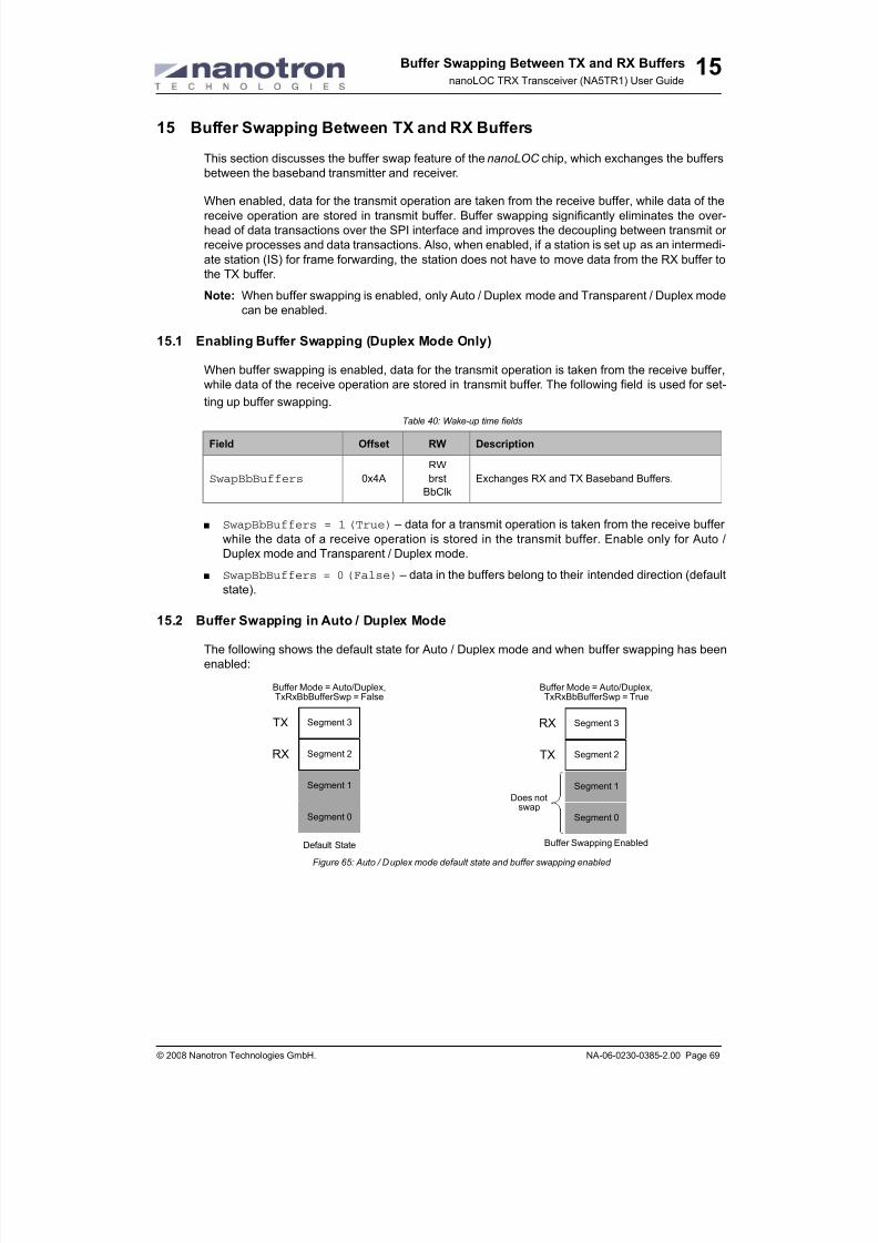
8/20/2019 nanoLOC NA5TR1 UserGuide
http://slidepdf.com/reader/full/nanoloc-na5tr1-userguide 85/325
Buffer Swapping Between TX and RX Buffers
nanoLOC TRX Transceiver (NA5TR1) User Guide
© 2008 Nanotron Technologies GmbH. NA-06-0230-0385-2.00 Page 69
15
15 Buffer Swapping Between TX and RX Buffers
This section discusses the buffer swap feature of the nanoLOC chip, which exchanges the buffers
between the baseband transmitter and receiver.
When enabled, data for the transmit operation are taken from the receive buffer, while data of thereceive operation are stored in transmit buffer. Buffer swapping significantly eliminates the over-
head of data transactions over the SPI interface and improves the decoupling between transmit or
receive processes and data transactions. Also, when enabled, if a station is set up as an intermedi-
ate station (IS) for frame forwarding, the station does not have to move data from the RX buffer to
the TX buffer.
Note: When buffer swapping is enabled, only Auto / Duplex mode and Transparent / Duplex mode
can be enabled.
15.1 Enabling Buffer Swapping (Duplex Mode Only)
When buffer swapping is enabled, data for the transmit operation is taken from the receive buffer,
while data of the receive operation are stored in transmit buffer. The following field is used for set-
ting up buffer swapping.
+ SwapBbBuffers = 1 (True) – data for a transmit operation is taken from the receive buffer
while the data of a receive operation is stored in the transmit buffer. Enable only for Auto /
Duplex mode and Transparent / Duplex mode.
+ SwapBbBuffers = 0 (False) – data in the buffers belong to their intended direction (default
state).
15.2 Buffer Swapping in Auto / Duplex Mode
The following shows the default state for Auto / Duplex mode and when buffer swapping has been
enabled:
Figure 65: Auto / Duplex mode default state and buffer swapping enabled
Table 40: Wake-up time fields
Field Offset RW Description
SwapBbBuffers 0x4A
RW
brst
BbClk
Exchanges RX and TX Baseband Buffers.
Segment 3
Segment 2
Segment 1
Segment 0
Buffer Mode = Auto/Duplex,TxRxBbBufferSwp = False
TX
RX
Segment 3
Segment 2
Segment 1
Segment 0
Buffer Mode = Auto/Duplex,TxRxBbBufferSwp = True
RX
TX
Does notswap
Default State Buffer Swapping Enabled

8/20/2019 nanoLOC NA5TR1 UserGuide
http://slidepdf.com/reader/full/nanoloc-na5tr1-userguide 86/325
Buffer Swapping Between TX and RX Buffers
nanoLOC TRX Transceiver (NA5TR1) User Guide
Page 70 NA-06-0230-0385-2.00 © 2008 Nanotron Technologies GmbH.
15
15.3 Buffer Swapping in Transparent / Duplex Mode
The following shows the default state for Transparent / Duplex mode and when buffer swapping
has been enabled:
Figure 66: Auto / Transparent mode default state and buffer swapping enabled
15.4 Buffer Swapping and Frame Forwarding
To eliminate the overhead of double data transactions over the SPI interface using store and for-
ward algorithm Buffer Swapping can be used. This results in less time wasted with SPI communi-
cation and saves electrical energy.
When MACFrames are to be forwarded, the value of SwapBbBuffers has to be inverted after a
reception but before the next (forwarding) transmission of the MACFrame's (payload) data. This
eliminates three operations – reading out the data from the receive buffer, storing it in the external
microcontroller, and writing it back in the transmit buffer.
15.5 Buffer Swapping and Short MACFrames
Buffer swapping can be used if two short MACFrames have to be transmitted or received in a close
sequence with a short time gap and the external microcontroller is not able to deliver or consume
data in the short time gap between two frames.
The buffer swapping feature eliminates SPI interface transactions for the data of short MAC-
Frames. Short MACFrames in Auto baseband mode are when the payload size is less than or
equal to 128 bytes. Short MACFrames in Transparent baseband mode are when the number of
transparent bytes is less than or equal to 256 bytes.
When frames have to be transmitted or received in close sequence, the value of SwapBbBuffers
has to be inverted between the two frames in sequence. Data for both packets can be written to
memory before the first one is transmitted or two packets can be received completely before the
data of both is read out.
Note: This feature can be used in the Duplex mode and only if the payload size is 128 bytes in
Auto baseband mode or if the frame size is 256 bytes in Transparent mode.
Segment 3
Segment 2
Segment 1
Segment 0
Buffer Mode = Transparent/Duplex,TxRxBbBufferSwp = False
TX
RX
Segment 3
Segment 2
Segment 1
Segment 0
Buffer Mode = Transparent/Duplex,TxRxBbBufferSwp = True
Default State Buffer Swapping Enabled
RX
TX

8/20/2019 nanoLOC NA5TR1 UserGuide
http://slidepdf.com/reader/full/nanoloc-na5tr1-userguide 87/325
Buffer Control Timing
nanoLOC TRX Transceiver (NA5TR1) User Guide
© 2008 Nanotron Technologies GmbH. NA-06-0230-0385-2.00 Page 71
16
16 Buffer Control Timing
This section describes the control timing for transmit and receive buffers.
16.1 Transmit Buffer Control Timing
Before transmitting a packet, the external microcontroller software fills up both upper and lower
transmit buffer segments with data. After each data transaction, the corresponding buffer com-
mand is issued. The software then initiates the transmission of a packet.
Data for transmission is taken from the transmit buffers, but always beginning with the lower buffer
segment (Buffer[0]). The buffer ready flag indicates that a buffer segment has been emptied
and is ready to be filled up again. When the number of MACFrame (payload) data bytes is not an
integer number of the buffer segment size, the buffer ready flag is also triggered when the last byte
of the frame has been taken from a buffer segment. In this case, it is not required to fill this buffer
part up completely, but it is mandatory to issue the buffer command.
A typical transmit buffer control timing is illustrated below.
Figure 67: Transmit timing
A transmit underrun exception occurs (TxUnderrun) when the transmitter tries to send out data
from a buffer segment that was not beforehand filled up properly. The transmit operation runs out
of data and cannot be completed. The flag informs the software, which usually treats the exception
in its protocol stack.
16.2 Receive Buffer Control Timing
Before a packet can be received, software starts the reception of a packet. If the receiver detects a
packet, the MACFrame (payload) data is stored in the receive buffer segment, but always begin-
ning with the lower buffer segment (Buffer[0]). When the receiver has filled up a buffer seg-ment, the corresponding buffer ready flag is triggered. The corresponding receive buffer can be
emptied by software, which was indicated by the flag.
External Microcontroller Software
MACFrame
MACFrame (Payload) Data
Data are taken from transmit buffers
Packet Begin Packet End
TxBuffer[0]
TxBuffer[1]
TxBuffer[0]
TxBuffer[1]
TxBuffer[0]
[0] [1][0]
[0][1] [0]
t
t
W r i t e
T x
B u
f f e r [ 0
]
W r i t e
T x
B u
f f e r [ 1
]
W r i t e
T x
B u
f f e r [ 0
]
[1][1]
W r i t e
T x
B u
f f e r [ 1
]
[0][0]
W r i t e
T x
B u
f f e r [ 0
]
P a c
k e
t t r a n s m
i s s
i o n
i s s
t a r t e
d

8/20/2019 nanoLOC NA5TR1 UserGuide
http://slidepdf.com/reader/full/nanoloc-na5tr1-userguide 88/325
Buffer Control Timing
nanoLOC TRX Transceiver (NA5TR1) User Guide
Page 72 NA-06-0230-0385-2.00 © 2008 Nanotron Technologies GmbH.
16
When the last byte has been read from a receive buffer segment, the software issues the receive
buffer ready command to indicate to the receiver that the buffer part has been read out completely.
If the number of MACFrame (payload) data bytes is not an integer number of the buffer part size,
the buffer ready flag is also triggered when the last byte of the frame has been stored in a buffer
part. In this case, it is not required to read out this buffer segment completely, but it is mandatory to
issue the buffer command.
A typical receive buffer control timing is illustrated below.
Figure 68: Receive timing
A receive overflow exception occurs (RxOverflow ) when the receiver tries to store a byte in a
buffer part that was not indicated as empty. The receive operation causes a data overflow and can-
not be completed properly. The flag informs the software, which usually treats the exception in its
protocol stack.
External Microcontroller Software
MACFrame
MACFrame (Payload) Data
Data are taken from receive buffers
Packet Begin Packet End
RxBuffer[0]
RxBuffer[1]
RxBuffer[0]
RxBuffer[1]
RxBuffer[0]
[0] [0]
t
t
R e a
d T x
B u
f f e r [ 0
]
[1] [1]
R e a
d T x
B u
f f e r [ 1
]
[0] [0]
R e a
d T x
B u
f f e r [ 0
]
[1] [0]
R e a
d T x
B u
f f e r [ 1
]
R e a
d T x
B u
f f e r [ 0
]
P a c k e
t t r a n s m
i s s
i o n
i s s
t a r t e
d
[1] [0]

8/20/2019 nanoLOC NA5TR1 UserGuide
http://slidepdf.com/reader/full/nanoloc-na5tr1-userguide 89/325
Buffer Access Synchronization
nanoLOC TRX Transceiver (NA5TR1) User Guide
© 2008 Nanotron Technologies GmbH. NA-06-0230-0385-2.00 Page 73
17
17 Buffer Access Synchronization
This section describes the flags and commands used for buffer access synchronization.
17.1 Flags and Commands
To avoid underrun or overflow exceptions of TX or RX data, the delivery or consumption of data by
an external microcontroller must be synchronized to the transmit or receive data rate. Conse-
quently, each TX and RX buffer is divided into two parts or blocks of equal length – an upper part
and a lower part. Additionally, each buffer has a flag and a command to control the data traffic to
and from the buffers. An example buffer is illustrated below:
Figure 69: Example buffer showing upper and lower parts with flags and commands
Note: The size of the buffer depends on the selected buffer configuration mode.
A flag-command pair is provided for each buffer segment (lower and upper) and for each direction
(transmit and receive).
17.2 Receive and Transmit Flags
Flags indicate to the software that buffers are ready for a data transfer and are not accessed by the
transceiver baseband. Usually flags are enabled as interrupts so that the software can react to a
triggered flag as quickly as possible. The following tables lists the receive and transmit flags.
BufferRdy[0]
Buffer[0]
BufferCmd[0]
BufferRdy[1]
Buffer[1]
BufferCmd[1]
Upper buffer segment
Lower buffer segment
= command
= interrupt
Table 41: Receive flags
Flag Description
RxBufferRdy[0]Indicates to the software that RxBuffer[0] (lower segment) has been filled
up with data by a receive operation.
RxBufferRdy[1] Indicates to the software thatRxBuffer[1]
(upper segment) has beenfilled up with data by a receive operation.
RxOverflow
Indicates to the software that a buffer part has been accessed by the
receiver, but was not ready to store data (a receive buffer command was not
issued in time).
Table 42: Transmit flags
Flag Description
TxBufferRdy[0]Indicates to the software that TxBuffer[0] (lower segment) has been
emptied by a transmit operation and is ready to store new data.
TxBufferRdy[1]Indicates to the software that TxBuffer[1] (upper segment) has been
emptied by a transmit operation and is ready to store new data.
TxUnderrunFlag which indicates to the software that a buffer part has been accessed bythe transmitter but was not ready for transmission (means that a transmit
buffer command was not issued in time).

8/20/2019 nanoLOC NA5TR1 UserGuide
http://slidepdf.com/reader/full/nanoloc-na5tr1-userguide 90/325
Buffer Access Synchronization
nanoLOC TRX Transceiver (NA5TR1) User Guide
Page 74 NA-06-0230-0385-2.00 © 2008 Nanotron Technologies GmbH.
17
17.3 Receive and Transmit Commands
Commands are issued after a data transaction and indicate to the transceiver baseband that data
is ready for transmission or buffers are ready to store received data. The following tables lists the
receive and transmit commands.
The following diagram shows the flags and commands for buffer access synchronization.
Figure 70: Flags and commands for buffer access synchronization
Note: Flags and commands are always related to their buffer segments, independent of buffer
size. Also, transmit buffer overflows are severe software errors and are not implemented.
Table 43: Receive Commands
Command Description
RxBufferCmd[0]
Indicates to the transceiver that RxBuffer[0] (lower segment) has been
read out and the buffer is now ready to store new data of a receive opera-
tion.
RxBufferCmd[1]
Indicates to the transceiver that RxBuffer[1] (upper segment) has been
read out and the buffer is now ready to store new data of a receive opera-
tion.
Table 44: Transmit Commands
Command Description
TxBufferCmd[0]Indicates to the transceiver that TxBuffer[0] (lower segment) has been
filled up and data is now ready for transmission.
TxBufferCmd[1]Indicates to the transceiver that TxBuffer[1] (upper segment) has been
filled up and data is now ready for transmission.
Software
External Microcontroller TRX
Transmitter/Receiver
Buffer Management Unit
Overflow / Underrun
BufferRdy[0]
Buffer[0]
(Lower segment)
BufferCmd[0]
BufferRdy[1]
Buffer[1]
(upper segment)
BufferCmd[1]

8/20/2019 nanoLOC NA5TR1 UserGuide
http://slidepdf.com/reader/full/nanoloc-na5tr1-userguide 91/325
Bit Processing
nanoLOC TRX Transceiver (NA5TR1) User Guide
© 2008 Nanotron Technologies GmbH. NA-06-0230-0385-2.00 Page 75
18
18 Bit Processing
This section describes the methods used in the nanoLOC chip for bit error detection, forward error
correction, bit scrambling, retransmission, and encryption.
18.1 Bit Stream Processes
Before application data is sent out over the air interface, several bit manipulations are performed in
the transmitter to increase reliability and security. These include:
1 Cyclic Redundancy Check (CRC), which is added to the MACFrame for error detection.
2 Encryption, which is optionally applied to the Data and CRC2 fields of the MACFrame.
3 Bit scrambling with a PRN-sequence.
4 Forward Error Correction (FEC) coding, which is optionally applied.
In the receiver, the reverse process is carried out. The following illustrates the processes:
Figure 71: Bit processing in transmitter and receiver
Note: CRC and bit scrambling processes are mandatory, while FEC and encryption can be
enabled by the application.
18.2 Cyclic Redundancy Check (CRC)
The purpose of the CRC scheme is to detect bit errors occurring during transmission. The CRC
field is a 16 or 32 bit field containing a Cyclic Redundancy Check. Two CRC fields are defined in
the MACFrame: CRC1 and CRC2.
Figure 72: CRC fields in MACFrame
18.2.1 CRC1 Field
The CRC1 value is calculated over the following MACFrame header fields: TypeCode, Address1,
Address2, Length, and FrameControl. It is not calculated over the ScrInit and Crypt fields. The
CRC1 is appended to MACFrame header fields and transmitted with the LSB first.
18.2.2 CRC2 Field
The CRC2 value, which is optional, is calculated over the Data field of Data and Brdcast packets.Different polynomials of 16 or 32 bit lengths are defined and can be selected for the CRC2. The
CRC2 is appended to the Data field of the MACFrame and transmitted with the LSB first.
CRC Generation Encryption Scrambling FEC Encoding
CRC Checking Decryption Descrambling FEC Decoding
RF Interface
MACFrame to transmit
Received MACFrame
Optional Mandatory
CRC1FrameControl
Length Address2 Address1TypeCode CRC2Data

8/20/2019 nanoLOC NA5TR1 UserGuide
http://slidepdf.com/reader/full/nanoloc-na5tr1-userguide 92/325
Bit Processing
nanoLOC TRX Transceiver (NA5TR1) User Guide
Page 76 NA-06-0230-0385-2.00 © 2008 Nanotron Technologies GmbH.
18
18.2.3 CRC Types 1, 2, and 3
Three CRC types are defined – CRC type 1, CRC type 2, and CRC type 3. The CRC1 field uses
only CRC type 1 whereas the CRC2 field can use any of the three CRC types or use none. A user
application can select an appropriate CRC type to satisfy error detection requirements or specific
customer demands.
+ CRC type 1 (ISO/IEC 3309, CCITT X.25,X.75, ETS 300 125)
Length . . . . . . . . . . . . . . . . . 16 bit
Polynomial . . . . . . . . . . . . . . 216+212+25+1
Initial value of LFSR . . . . . . 0xFFFF
CRC. . . . . . . . . . . . . . . . . . . Ones complement of the LFSR
Check value of LFSR. . . . . . 0xF0B8
+ CRC type 2 (IEC 60870-5-1)
Length . . . . . . . . . . . . . . . . . 16 bit
Polynomial . . . . . . . . . . . . . . 2
16
+2
13
+2
12
+2
11
+2
10
+2
8
+2
6
+2
5
+2
2
+1Initial value of LFSR . . . . . . 0x0000
CRC. . . . . . . . . . . . . . . . . . . Ones complement of the LFSR
Check value of LFSR. . . . . . 0xA366
+ CRC type 3 (CCITT-32, Ethernet)
Length . . . . . . . . . . . . . . . . . 32 bit
Polynomial . . . . . . . . . . . . . . 232+226+223+222+216+212+211+210+28+27+25+24+22+2+1
Initial value of LFSR . . . . . . 0xFFFFFFFF
CRC. . . . . . . . . . . . . . . . . . . Content of the LFSR
Check value of LFSR. . . . . . 0xCBF43926
18.3 Bit Scrambling
Before transmission, all fields of the MACFrame, except the ScrambIerInit field, are scrambled with
a PRN-sequence to randomize the data into highly redundant patterns and to minimize the proba-
bility of large zero patterns. At the receiver, the received data is descrambled using the same PRN-
sequence that was generated in the transmitter.
The PRN-sequence is generated with the polynomial g(D)= D7+D4+D0 (221 in octal representa-
tion) and is subsequently EXORed with the MACFrame. Before each transmission, the shift regis-
ter must be initialized with a 7 bit value by the transmitting station. The value should be changed
for every new packet, even for retransmissions.
Note: No scrambling is performed when an initialization value of zero is programmed.
The initial value of the shift register is loaded in the ScrambIerInit field of the packet (LSB first) and
sent over the air interface. During reception of a MACFrame, the shift register of the receiver
descrambler is initialized with the bits from the ScramblerInit field. Consequently, the remaining
fields are subsequently EXORed with the same PRN-sequence.
18.4 Forward Error Correction (FEC)
Using Forward Error Correction (FEC) scheme on the MACFrame reduces the number of retrans-
missions. However, in a reasonable error-free environment, FEC gives unnecessary overhead that
reduces the throughput. Therefore, the user application must decide whether or not it should be
applied. If FEC is applied, all MACFrame fields are elements of the FEC algorithm.
The FEC scheme is a (7,4) shortened Hamming code and consists of 4 data bits and 3 parity bits.The parity bits are generated with the polynomial g(D)=D3+D+1. The LFSR generating the parity
bits is illustrated below.

8/20/2019 nanoLOC NA5TR1 UserGuide
http://slidepdf.com/reader/full/nanoloc-na5tr1-userguide 93/325
Bit Processing
nanoLOC TRX Transceiver (NA5TR1) User Guide
© 2008 Nanotron Technologies GmbH. NA-06-0230-0385-2.00 Page 77
18
The code is able to correct single bit errors and detect double bit errors within a codeword. Conse-
quently, a 14 bit code word can contain 2 bit errors even if the bit errors are consecutive. This is
achieved through the interleaving scheme.
The receiver informs the LLC about the number of bit errors that have occurred during the recep-
tion and correction of a Data packet. This bit error number combined with the Length field is anindication of the BER at the physical interface.
18.5 Encryption
The encryption process is applied to the Data and CRC2 fields of a MACFrame. This process is
based on a stream cipher with a symmetric key scheme. The stream cipher sequence bits are
XORed with the data bits before transmission or after reception. The cipher stream is re-initialized
for every packet (re-)transmission. Since the process is reversible, the same cipher stream is used
for encryption and decryption. Consequently, the same input values are required for the generator
in both the transmitter and the receiver. The 32 bit clock value and the 48 bit address are publicly
known while the 128 bit secret key is generated during the encryption negotiation process and
never disclosed.
Note: For more details, see 19.1.1. Stream Cipher Function on page 79.
To keep the probability very low of a successful correlation attack, the same cipher stream is never
used twice. The 32 bit clock value is changed (at least incremented by one) for every new packet
transmission.

8/20/2019 nanoLOC NA5TR1 UserGuide
http://slidepdf.com/reader/full/nanoloc-na5tr1-userguide 94/325
Bit Processing
nanoLOC TRX Transceiver (NA5TR1) User Guide
Page 78 NA-06-0230-0385-2.00 © 2008 Nanotron Technologies GmbH.
18
Intentionally Left Blank
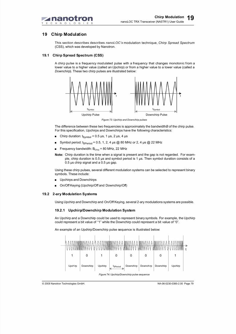
8/20/2019 nanoLOC NA5TR1 UserGuide
http://slidepdf.com/reader/full/nanoloc-na5tr1-userguide 95/325
Chirp Modulation
nanoLOC TRX Transceiver (NA5TR1) User Guide
© 2008 Nanotron Technologies GmbH. NA-06-0230-0385-2.00 Page 79
19
19 Chirp Modulation
This section describes describes nanoLOC’s modulation technique, Chirp Spread Spectrum
(CSS), which was developed by Nanotron.
19.1 Chirp Spread Spectrum (CSS)
A chirp pulse is a frequency modulated pulse with a frequency that changes monotonic from a
lower value to a higher value (called an Upchirp) or from a higher value to a lower value (called a
Downchirp). These two chirp pulses are illustrated below:
Figure 73: Upchirp and Downchirp pulses
The difference between these two frequencies is approximately the bandwidth B of the chirp pulse.
For this specification, Upchirps and Downchirps have the following characteristics:
+ Chirp duration: tSymbol = 0.5 µs, 1 µs, 2 µs, 4 µs
+ Symbol period: tSPeriod = 0.5, 1, 2, 4 µs @ 80 MHz or 2, 4 µs @ 22 MHz
+ Frequency bandwidth: BChirp = 80 MHz, 22 MHz
Note: Chirp duration is the time when a signal is present and the gap is not regarded. For exam-
ple, chirp duration is 0.5 µs and symbol period is 1 µs. Then symbol duration consists of a0.5 µs chirp signal and a 0.5 µs gap.
Using these chirp pulses, several different modulation systems can be selected to represent binary
symbols. These include:
+ Upchirps and Downchirps
+ On/Off Keying (Upchirp/Off and Downchirp/Off)
19.2 2-ary Modulation Systems
Using Upchirp and Downchirp and On/Off Keying, several 2-ary modulations systems are possible.
19.2.1 Upchirp/Downchirp Modulation System
An Upchirp and a Downchirp could be used to represent binary symbols. For example, the Upchirp
could represent a bit value of “1” while the Downchirp could represent a bit value of “0”.
An example of an Upchirp/Downchirp pulse sequence is illustrated below:
Figure 74: Upchirp/Downchirp pulse sequence
tSymboltSymbol
t
Downchirp PulseUpchirp Pulse
t
1 0 1 0 0 0 0 1
tSPeriod
t
Upchirp Downchirp Downchirp Downchirp DownchirpUpchirp Upchirp

8/20/2019 nanoLOC NA5TR1 UserGuide
http://slidepdf.com/reader/full/nanoloc-na5tr1-userguide 96/325
Chirp Modulation
nanoLOC TRX Transceiver (NA5TR1) User Guide
Page 80 NA-06-0230-0385-2.00 © 2008 Nanotron Technologies GmbH.
19
19.2.2 Upchirp/Off Modulation System
Using On/Off Keying, an Upchirp/Off modulation system can be produced, where an Upchirp pulse
could represent a bit value of “1” while the absence of an Upchirp pulse (an “off” chirp pulse) could
represents a bit value of “0”. An example of an Upchirp/Off pulse sequence is illustrated below:
Figure 75: Upchirp/Off chirp pulse sequence
19.2.3 Downchirp/Off Modulation System
Using On/Off Keying, a Downchirp/Off modulation system can be produced, where a Downchirp
pulse could represent a bit value of “1”, while the absence of a Downchirp pulse (an “off” chirp
pulse) could represents a bit value of “0”. An example of a Downchirp/Off pulse sequence is illus-
trated below:
Figure 76: Downchirp/Off pulse sequence
19.2.4 Physical Channels and the On-Off Keying Modulation Systems
The two binary On/Off keying modulation systems (Upchirp/Off and Downchirp/Off) require only
Upchirp or Downchirp pulses. Consequently, these two different on-off keying systems can access
the same medium with low interference (0 < cross correlation < 0.5 ) to each other.
Both systems can operate in the same frequency channel, in the same physical range, and at the
same time but remain independent of each other. They can, therefore, be regarded as separated
physical channels.
1 0 1 0 0 0 0 1
tSPeriod
t
Upchirp Off Upchirp Off Off Off Upchirp
1 1 0 1 1 1 1 0
tSPeriod
t
Downchirp Off Downchirp Downchirp Downchirp Downchirp Off

8/20/2019 nanoLOC NA5TR1 UserGuide
http://slidepdf.com/reader/full/nanoloc-na5tr1-userguide 97/325
Local Oscillator
nanoLOC TRX Transceiver (NA5TR1) User Guide
© 2008 Nanotron Technologies GmbH. NA-06-0230-0385-2.00 Page 81
20
20 Local Oscillator
This section describes how to calibrate Local Oscillator frequency.
20.1 Purpose of the Local Oscillator
Switched capacitors are used to calibrate the Local Oscillator (LO) frequency. The total capaci-
tance of 22 capacitors plus the capacitance of the oscillating circuit are used to determine the fre-
quency. Each of the twelve capacitors can be separately switched on and off.
The capacitor values are stored for both receive and transmit modes inside the Local Oscillator
controller. A single control signal permits the quick tuning of the Local Oscillator to the correspond-
ing target frequency.
During normal operation, the Local Oscillator controller powers the Local Oscillator and sets the
receive or transmit frequency automatically, depending on the operation of the MAC controller.
To compensate for die temperature and supply voltage drifts, as well as for fabrication process
variations, the Local Oscillator controller supports an automatic Local Oscillator frequency adjust-
ment with a minimum of required software interaction. The Local Oscillator frequency is compared
with the internal crystal quartz frequency while the implemented successive approximation algo-
rithm determines the capacitor switch values (on or off), depending on the comparison result and a
value for the target frequency. The capacitor switch values (on or off) can be read out and written to
again if the automatic readjustment is not required after a power down cycle.
20.2 Calibrating the Local Oscillator Frequency
The software interaction of the Local Oscillator frequency calibration is as follows:
1 Start up the baseband clock and reset the digital baseband controller, if required.Note: Steps 2 and 3 can be performed simultaneously.
2 Enable the LO circuitry, the LO divider, and the LO adjustment clock as follows:
a. Set EnableLO = True.
b. Set EnableLOdiv10 = True.
3 Switch the Local Oscillator into transmit mode by setting UseLoRxCaps = False.
4 Wait 24 µs.
5 Set the 16 bit value for the TX target frequency fTarget as follows:
The adjustment procedure starts automatically when writing to the upper bits of the value.
Frequency example: fTarget = 2.44175 GHz:
6 Wait 13 ms (baseband timer could be used).
Note: When fast tuning mode is used, then wait time is reduced to 6 ms. See 26.26.
0x1C – RF Local Oscillator Controls on page 157 for details on using fast tuning
mode.7 Optionally, the resulting value LoTxCapsValue can be put into a variable to be used after power
down mode. During powering up, this value can then be reused:
Table 45: Value for fTarget
fTarget RfLoAdjIncValue
2.44175 GHz 0x685A
Lo T et Va lu earg round LoDiv10
16---------------------- 12–⟨ ⟩ 8192⋅
⎝ ⎠
⎛ ⎞=
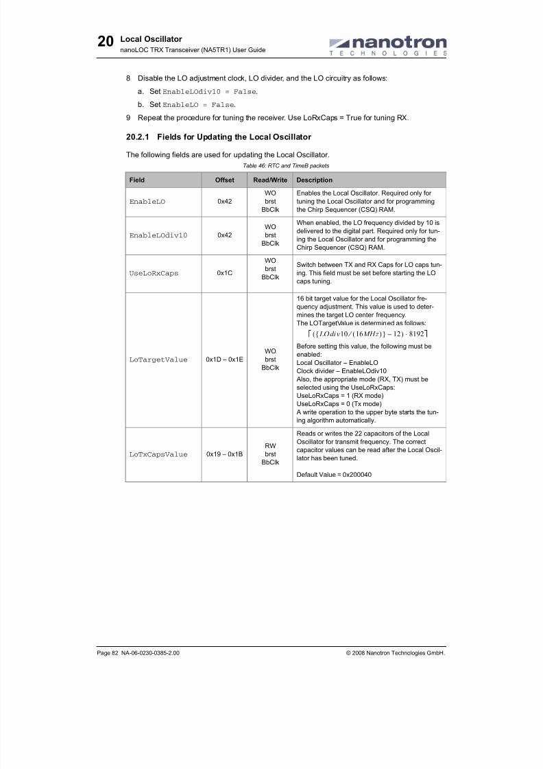
8/20/2019 nanoLOC NA5TR1 UserGuide
http://slidepdf.com/reader/full/nanoloc-na5tr1-userguide 98/325
Local Oscillator
nanoLOC TRX Transceiver (NA5TR1) User Guide
Page 82 NA-06-0230-0385-2.00 © 2008 Nanotron Technologies GmbH.
20
8 Disable the LO adjustment clock, LO divider, and the LO circuitry as follows:
a. Set EnableLOdiv10 = False.
b. Set EnableLO = False.
9 Repeat the procedure for tuning the receiver. Use LoRxCaps = True for tuning RX.
20.2.1 Fields for Updating the Local Oscillator
The following fields are used for updating the Local Oscillator.
Table 46: RTC and TimeB packets
Field Offset Read/Write Description
EnableLO 0x42
WO
brst
BbClk
Enables the Local Oscillator. Required only for
tuning the Local Oscillator and for programming
the Chirp Sequencer (CSQ) RAM.
EnableLOdiv10 0x42
WO
brst
BbClk
When enabled, the LO frequency divided by 10 is
delivered to the digital part. Required only for tun-
ing the Local Oscillator and for programming the
Chirp Sequencer (CSQ) RAM.
UseLoRxCaps 0x1C
WO
brst
BbClk
Switch between TX and RX Caps for LO caps tun-
ing. This field must be set before starting the LO
caps tuning.
LoTargetValue 0x1D – 0x1E
WO
brst
BbClk
16 bit target value for the Local Oscillator fre-
quency adjustment. This value is used to deter-
mines the target LO center frequency.
The LOTargetValue is determined as follows:
Before setting this value, the following must be
enabled:
Local Oscillator – EnableLO
Clock divider – EnableLOdiv10
Also, the appropriate mode (RX, TX) must be
selected using the UseLoRxCaps:
UseLoRxCaps = 1 (RX mode)
UseLoRxCaps = 0 (Tx mode)
A write operation to the upper byte starts the tun-
ing algorithm automatically.
LoTxCapsValue 0x19 – 0x1B
RW
brst
BbClk
Reads or writes the 22 capacitors of the Local
Oscillator for transmit frequency. The correct
capacitor values can be read after the Local Oscil-
lator has been tuned.
Default Value = 0x200040
LO di v10 16 MHz ( ) ⁄ { } 12–( ) 8192⋅

8/20/2019 nanoLOC NA5TR1 UserGuide
http://slidepdf.com/reader/full/nanoloc-na5tr1-userguide 99/325
RF Transmitter
nanoLOC TRX Transceiver (NA5TR1) User Guide
© 2008 Nanotron Technologies GmbH. NA-06-0230-0385-2.00 Page 83
21
21 RF Transmitter
This section describes the adjustment of the Baseband filter frequency, the power amplifier bias
current, and the output power of the transmitter.
21.1 Adjusting the Baseband Filter Frequency
Why Adjust this Frequency?
The frequency of the Baseband filter (chirp DAC filter) must be adjusted because of process devia-
tions of the resistor values and capacitor values.
Realization
+ A fixed relationship exists between the RC-Oscillator (RCOSC) frequency and the Baseband
filter frequency because both circuits use the same resistor and capacitor types.
+ The user can set the 4 bit value ChirpFilterCaps to adjust the RC-oscillator/Baseband filter
frequency.
+ ChirpFilterCaps is used for adjusting the RCOSC frequency in comparison with the system
clock.
+ The algorithm has to be implemented in software.
To Adjust the RC-Oscillator Baseband Filter Frequency1
1 Set the start value to ChirpFilterCaps = 0b0110.
2 Enable the RC-Oscillator (RCOSC) by setting TxFctEn = True.
3 Ignore at least 4 cycles of RCOSC output frequency by waiting 20 µs (baseband timer can be
used).
4 Count the cycles of the baseband system clock for next cref cycles of RCOSC as follows:
a. Start the counter by setting StartFctMeasure = True.
b. Wait at least .
c. Read out the counter value from the FctPeriod field.
d. Run this sequence cref times, accumulating the counter value after each run.
5 Decision (for cref RCOSC cycles):
a. If the number of system cycles are greater than the following:
(For cref = 4, n1 = 172)
then decrease value for RfTxChirpFilterCaps.
b. If the number of system cycles are less than the following:
(For cref = 4, n2 = 156)
then increase value for RfTxChirpFilterCaps (ChirpFilterCaps).
c. If the counter value from step 4d above is between n1 and n2, then stop the calibration.
or if n ≤ 172 after the previous counter value was > 172, or if n ≥ 156 after the previous
counter value was < 156, then:
Set FctClockEn = False.
1. Cycle reference frequency definitions:
VariableDefinitionValuecref Cycle reference: number of RCOSC reference cycles.≥ 4
f ref Frequency reference: reference frequency of RCOSC.400 kHz
1
f re f
---------
n1 cre f
43⋅=
n2 cre f
39⋅=

8/20/2019 nanoLOC NA5TR1 UserGuide
http://slidepdf.com/reader/full/nanoloc-na5tr1-userguide 100/325
RF Transmitter
nanoLOC TRX Transceiver (NA5TR1) User Guide
Page 84 NA-06-0230-0385-2.00 © 2008 Nanotron Technologies GmbH.
21
21.2 Setting the Power Amplifier Bias Current
To set the PA Bias Current
+ Set the following:
21.3 Adjusting the Transmitter Output Power
21.3.1 Output Power Control
The typical characteristics of the output power control (as set by RfTxOutputPower) measured at
the SMA connector of the nanoLOC RF Module is shown below. The typical output power values
are listed in table Table 48 on page 84.
Figure 4: nanoLOC (NA5TR1) output power control measured at SMA connector of RF Test Module
Table 47: Setting PA bias current
Switch Setting
RfTxPaBiasAdj (TxPaBias) 000
Table 48: Typical output power for RfTxOutputPower register values
RegisterValue
Pout /dBm
RegisterValue
Pout /dBm
RegisterValue
Pout /dBm
RegisterValue
Pout /dBm
0 -36.20 16 -23.28 32 -12.07 48 -3.33
1 -35.30 17 -22.48 33 -11.41 49 -2.87
2 -34.47 18 -21.75 34 -10.80 50 -2.45
3 -33.65 19 -21.03 35 -10.20 51 -2.05
4 -32.83 20 -20.31 36 -9.61 52 -1.66
5 -32.02 21 -19.60 37 -9.03 53 -1.28
6 -31.21 22 -18.89 38 -8.46 54 -0.92
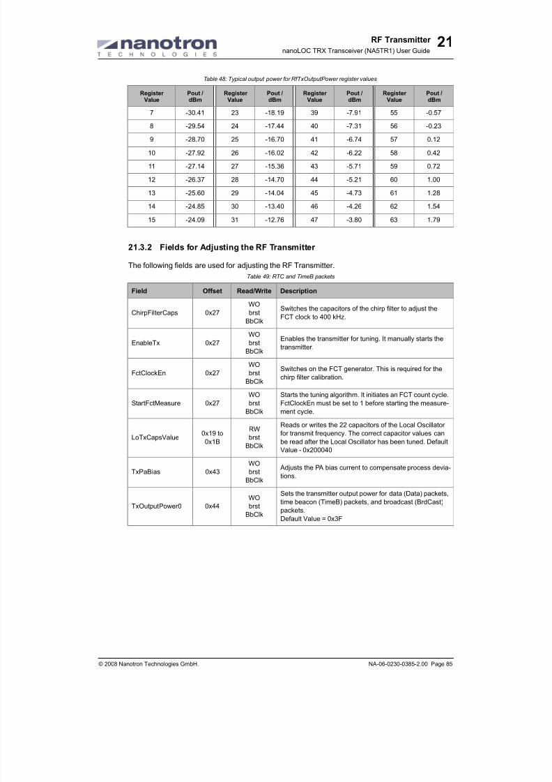
8/20/2019 nanoLOC NA5TR1 UserGuide
http://slidepdf.com/reader/full/nanoloc-na5tr1-userguide 101/325
RF Transmitter
nanoLOC TRX Transceiver (NA5TR1) User Guide
© 2008 Nanotron Technologies GmbH. NA-06-0230-0385-2.00 Page 85
21
21.3.2 Fields for Adjusting the RF Transmitter
The following fields are used for adjusting the RF Transmitter.
7 -30.41 23 -18.19 39 -7.91 55 -0.57
8 -29.54 24 -17.44 40 -7.31 56 -0.23
9 -28.70 25 -16.70 41 -6.74 57 0.12
10 -27.92 26 -16.02 42 -6.22 58 0.42
11 -27.14 27 -15.36 43 -5.71 59 0.72
12 -26.37 28 -14.70 44 -5.21 60 1.00
13 -25.60 29 -14.04 45 -4.73 61 1.28
14 -24.85 30 -13.40 46 -4.26 62 1.54
15 -24.09 31 -12.76 47 -3.80 63 1.79
Table 49: RTC and TimeB packets
Field Offset Read/Write Description
ChirpFilterCaps 0x27
WO
brst
BbClk
Switches the capacitors of the chirp filter to adjust the
FCT clock to 400 kHz.
EnableTx 0x27
WO
brst
BbClk
Enables the transmitter for tuning. It manually starts the
transmitter.
FctClockEn 0x27
WO
brstBbClk
Switches on the FCT generator. This is required for the
chirp filter calibration.
StartFctMeasure 0x27
WO
brst
BbClk
Starts the tuning algorithm. It initiates an FCT count cycle.
FctClockEn must be set to 1 before starting the measure-
ment cycle.
LoTxCapsValue0x19 to
0x1B
RW
brst
BbClk
Reads or writes the 22 capacitors of the Local Oscillator
for transmit frequency. The correct capacitor values can
be read after the Local Oscillator has been tuned. Default
Value - 0x200040
TxPaBias 0x43
WO
brst
BbClk
Adjusts the PA bias current to compensate process devia-
tions.
TxOutputPower0 0x44WObrst
BbClk
Sets the transmitter output power for data (Data) packets,
time beacon (TimeB) packets, and broadcast (BrdCast)
packets.
Default Value = 0x3F
Table 48: Typical output power for RfTxOutputPower register values
RegisterValue
Pout /dBm
RegisterValue
Pout /dBm
RegisterValue
Pout /dBm
RegisterValue
Pout /dBm

8/20/2019 nanoLOC NA5TR1 UserGuide
http://slidepdf.com/reader/full/nanoloc-na5tr1-userguide 102/325
RF Transmitter
nanoLOC TRX Transceiver (NA5TR1) User Guide
Page 86 NA-06-0230-0385-2.00 © 2008 Nanotron Technologies GmbH.
21
Intentionally Left Blank

8/20/2019 nanoLOC NA5TR1 UserGuide
http://slidepdf.com/reader/full/nanoloc-na5tr1-userguide 103/325
Media Access Control Methods
nanoLOC TRX Transceiver (NA5TR1) User Guide
© 2008 Nanotron Technologies GmbH. NA-06-0230-0385-2.00 Page 87
22
22 Media Access Control Methods
This section describes various media access methods, including Direct Access (DA), Random
Access (CSMA/CA) and TDMA.
22.1 Symbols Definitions
The following symbol is used in this section:
+ MacArqCntMax
Note: These symbols are defined in Appendix 1: Attributes and Constants on page 289.
22.2 Direct Access (DA) Mode
A very simple way to access the media is with the Direct Access (DA) mode. Using this method, a
station that wants to access the media does not sense the carrier nor wait a specific period of timebefore accessing the media. However, collisions may occur with transmissions from other stations
or with noise sources using the same frequency bandwidth and located in the same range. Direct
access is, therefore, intended for protocols where the probability of collisions is very low. Applica-
tions of Direct Access include master-slave protocols and TDMA:
+ Master-Slave Protocols - A single master station allocates bandwidth for a slave station and it
assumes that there are no competitors for the media other than this master. The master then
polls a slave to request a Data packet. Only that polled station can transmit a Data packet. The
master station then waits for the Data packet a time-out interval and then polls this slave again
or else polls other slave stations. The poll command is transmitted to the slave via an LCMP
command in a Data packet.
+ TDMA - Time Slotted Media Access achieves bandwidth reservation through the use of dedi-
cated time slots.
Note: For more details, see 22.4. Time Slotted Access (TDMA) on page 94.
22.3 Random Access (CSMA/CA) Mode
22.3.1 General Description
Carrier Sense Multiple Access/Collision Avoidance (CSMA/CA) is an access method that promotes
fairness as all stations have equal probability of gaining access to the media. Fairness is main-
tained because each station must recontend for the media after every transmission.
CSMA works as follows:
1 A station that has data to transmit first senses the channel (CSMA) for a certain duration to
determine if the media is busy before transmitting a message.
2 If the channel is busy, the station attempts a retransmission at a later time.
3 If the channel is idle, the station waits a random period of time (a “backoff” time) and then
attempts again to acquire the media. This random backoff scheme avoids collisions (CA) as
much as possible.
4 The acquisition of the media is followed by the transmission of the Data packet.
5 This transmission is then acknowledged by the destination station with an Ack packet to allow
the transmitting station to determine if the transmission was successful. If an Ack packet was
not received, the transmission was deemed not successful.
6 This procedure is repeated until the transmission has been successful, a retransmissioncounter is exceeded, or a time-out is reached.
Note: For more details, see 22.3.4. Retransmissions on page 90.

8/20/2019 nanoLOC NA5TR1 UserGuide
http://slidepdf.com/reader/full/nanoloc-na5tr1-userguide 104/325
Media Access Control Methods
nanoLOC TRX Transceiver (NA5TR1) User Guide
Page 88 NA-06-0230-0385-2.00 © 2008 Nanotron Technologies GmbH.
22
The scheme for CSMA/CA is shown below.
Figure 5: CSMA/CA protocol (at transmitting station)
22.3.2 Carrier Sensing
The state of the media is determined by using physical and virtual carrier-sense functions:
+ Physical carrier sensing detects activity in the media via a bit detector unit and a RSSI (Receive
Signal Strength Indicator). For instance, if the bit detector senses chirp signals, then there is
communication activity in the media. The physical carrier sensing unit selects the output of either the bit detector or the RSSI or both. A station will continue sensing the media until the
media has been idle for at least a CIFS (Carrier sense InterFrame Space) period.
Medium = busy
Initiate transmissionof a data packet
N
Y
N
Y
CSMA/CA
Y
N
Y
Y N
N
Set randomrange to min
Set backup counter with random value
Decrement backoff counter if !zero
Medium = busy
Counter = zero
Double randomrange
Retransmissions= max
Incrementretransmission
counter
Transmit packet
Wait onacknowledge
Acknowledge = true
Flushpacket

8/20/2019 nanoLOC NA5TR1 UserGuide
http://slidepdf.com/reader/full/nanoloc-na5tr1-userguide 105/325
Media Access Control Methods
nanoLOC TRX Transceiver (NA5TR1) User Guide
© 2008 Nanotron Technologies GmbH. NA-06-0230-0385-2.00 Page 89
22
+ Virtual carrier sensing predicts if the media is allocated by detecting the TypeCode and Length
fields in packets transmitted by any station. These fields are used to indicate the amount of
time required to complete a transmission and are used by stations to adjust their NAVs (Net-
work Allocation Vector). A NAV is an indicator of the amount of time that must elapse until the
current transmission is complete and when the media can be sampled again to determine if the
media is idle.
A station updates its NAV with the indication from the Length field. If the error detection over the
MACFrame fails (that is CRC1 fails), then the NAV is set to “0” and physical carrier sensing is
applied until the NAV can be updated again.
If either the physical or virtual carrier sensing mechanisms indicate that the channel is busy, then
the channel is marked busy. Carrier sensing for Data, Brdcast, and TimeB packets is illustrated
below.
Figure 6: CSMA/CA Carrier Sense Timing diagram of Data, Brdcast and TimeB packets
The NAV can also be used as a mechanism for power saving. A station can be powered down for a
NAV period of time. However, if a station is powered down, it is unable to receive packets and, con-
sequently, cannot update its NAV.
22.3.3 Backoff Time
If the media is detected idle, the transmitting station waits a specific period of time before it reat-
tempts a transmission. This period is the contention window (CW) and is determined by a backoff
counter which counts defined time slots, each of which is a Backoff Time Slot (BTS). This is illus-
trated below, where BTS = 24 µs.
TypeCodeField
Data
Ack t
LengthField
} }
CIFSSIFS
NAV (Data)
Defer access
TypeCodeField
Brdcast, TimeB
t
LengthField
} }
CIFS
NAV (Brdcast, TimeB)
Defer access

8/20/2019 nanoLOC NA5TR1 UserGuide
http://slidepdf.com/reader/full/nanoloc-na5tr1-userguide 106/325
Media Access Control Methods
nanoLOC TRX Transceiver (NA5TR1) User Guide
Page 90 NA-06-0230-0385-2.00 © 2008 Nanotron Technologies GmbH.
22
Figure 7: Backoff procedure example
While the media is idle, a station decrements its backoff counter using physical carrier sensing until
the media again becomes busy. While the media is busy, the backoff counter is frozen until virtual
and physical carrier sensing detects that the media has again become idle. The state of the media
can, therefore, be determined at any time during a BTS.
A station can access the media and transmits a packet only when the backoff counter reaches “0”
and if the media is idle.
When a station makes the fi rst transmission attempt, the backoff counter is initialized with a
pseudo-random integer in the range of 0 to 7. For every new transmission attempt this range is
doubled, which is an exponential backoff. For the second transmission attempt, the backoff counter
is initialized with a pseudorandom integer in the range of 0 to 15; for the third attempt, it is initial-
ized in range of 0 to 31; and so on until the range reaches 0 to 255. The pseudo-
random integer is then drawn from the range of 0 to 255 for every new attempted retransmission.
22.3.4 Retransmissions
A retransmission is the repeated transmission of the same Data packet. If a transmitting station
does not receive an acknowledgement from a destination station, the Data packet must be retrans-
mitted. This failed acknowledgement can be either the absence of an Ack packet in response to a
Data packet or, in the case of a three-way handshake, the absence of a Clr2S packet in response
to a Req2S packet. Both cases are regarded as unsuccessful transmission attempts.
Note: See also 23.2. Error Correction (ARQ scheme) on page 99 and 22.3.5. Three-Way Hand-shake on page 91.
A transmitting station cannot determine the reason for any unsuccessful transmission attempt. It is
unable to detect, for instance, if a collision occurred or if the transmission path was disrupted. In
every case, a retransmission is required.
To limit the number of unsuccessful retransmission attempts, a retransmit counter counts the unac-
knowledged transmissions. When the maximum number of attempts is reached, as defined by the
MacArqCntMax attribute, no more retransmissions are made and the LLC is informed that the
maximum number of unsuccessful transmission attempts have been reached.
Note: Retransmission is applied only to Data packets. Brdcast and TimeB packets cannot be
retransmitted because they do not require an acknowledgement. In the latter case, resentpackets are never regarded as retransmitted, even if consecutively sent packets are identi-
cal.
t
BTS
Contention window
1 0
BTS
2
BTS
3
BTS
4
BTS
5
CIFS
Defer access
NAV
RSSI
Physicalcarrier sensing
Mediaaccess
Initialize backoff counter withrandom value in range 0-7
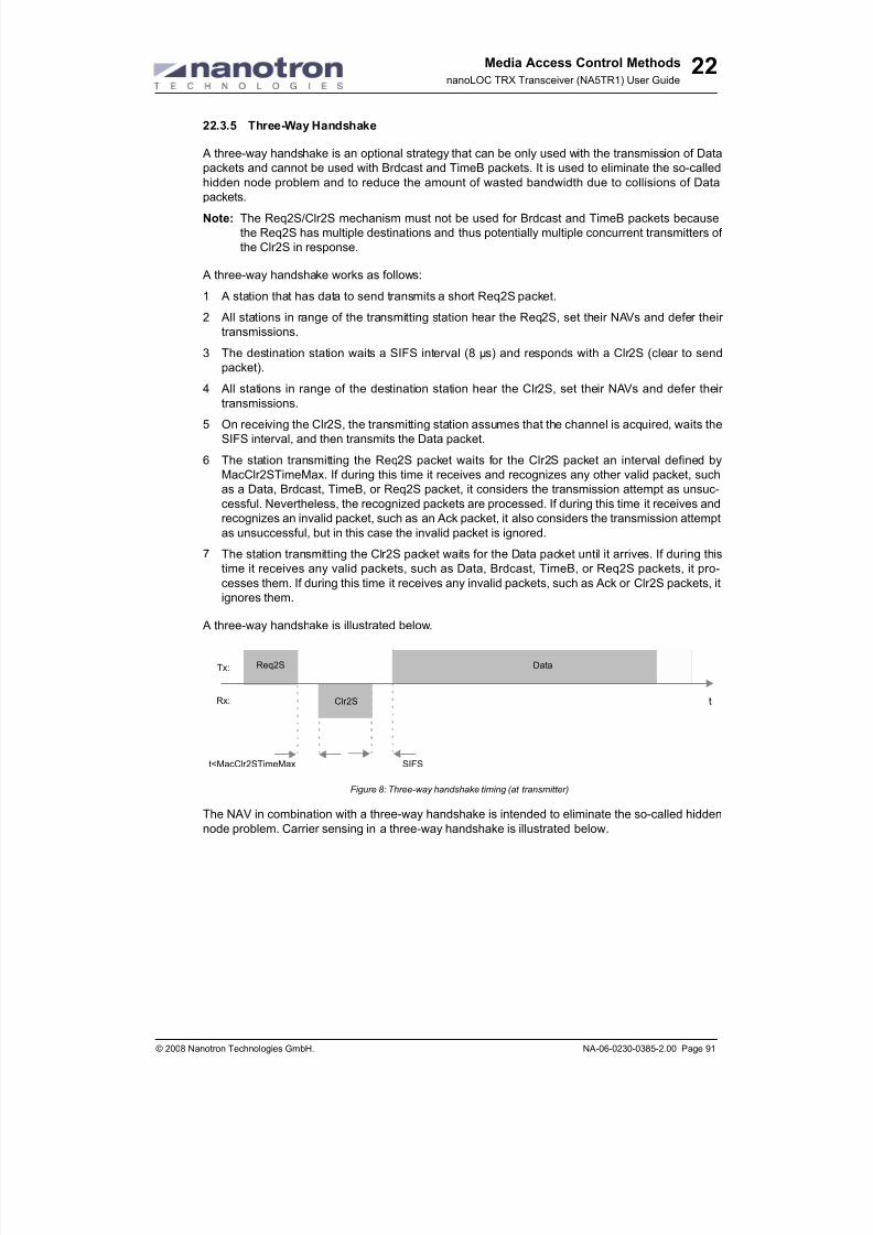
8/20/2019 nanoLOC NA5TR1 UserGuide
http://slidepdf.com/reader/full/nanoloc-na5tr1-userguide 107/325
Media Access Control Methods
nanoLOC TRX Transceiver (NA5TR1) User Guide
© 2008 Nanotron Technologies GmbH. NA-06-0230-0385-2.00 Page 91
22
22.3.5 Three-Way Handshake
A three-way handshake is an optional strategy that can be only used with the transmission of Data
packets and cannot be used with Brdcast and TimeB packets. It is used to eliminate the so-called
hidden node problem and to reduce the amount of wasted bandwidth due to collisions of Data
packets.
Note: The Req2S/Clr2S mechanism must not be used for Brdcast and TimeB packets because
the Req2S has multiple destinations and thus potentially multiple concurrent transmitters of
the Clr2S in response.
A three-way handshake works as follows:
1 A station that has data to send transmits a short Req2S packet.
2 All stations in range of the transmitting station hear the Req2S, set their NAVs and defer their
transmissions.
3 The destination station waits a SIFS interval (8 µs) and responds with a Clr2S (clear to send
packet).
4 All stations in range of the destination station hear the Clr2S, set their NAVs and defer their transmissions.
5 On receiving the Clr2S, the transmitting station assumes that the channel is acquired, waits the
SIFS interval, and then transmits the Data packet.
6 The station transmitting the Req2S packet waits for the Clr2S packet an interval defined by
MacClr2STimeMax. If during this time it receives and recognizes any other valid packet, such
as a Data, Brdcast, TimeB, or Req2S packet, it considers the transmission attempt as unsuc-
cessful. Nevertheless, the recognized packets are processed. If during this time it receives and
recognizes an invalid packet, such as an Ack packet, it also considers the transmission attempt
as unsuccessful, but in this case the invalid packet is ignored.
7 The station transmitting the Clr2S packet waits for the Data packet until it arrives. If during this
time it receives any valid packets, such as Data, Brdcast, TimeB, or Req2S packets, it pro-
cesses them. If during this time it receives any invalid packets, such as Ack or Clr2S packets, itignores them.
A three-way handshake is illustrated below.
Figure 8: Three-way handshake timing (at transmitter)
The NAV in combination with a three-way handshake is intended to eliminate the so-called hidden
node problem. Carrier sensing in a three-way handshake is illustrated below.
SIFS
DataTx:
Rx: t
Req2S
Clr2SClr2S
t<MacClr2STimeMax

8/20/2019 nanoLOC NA5TR1 UserGuide
http://slidepdf.com/reader/full/nanoloc-na5tr1-userguide 108/325
Media Access Control Methods
nanoLOC TRX Transceiver (NA5TR1) User Guide
Page 92 NA-06-0230-0385-2.00 © 2008 Nanotron Technologies GmbH.
22
Figure 9: Three-way handshake timing diagram
Note: The three-way handshake mechanism adds overhead inefficiency because of the additional
Req2S and Clr2S packets required for this strategy. Also, if this strategy is used, every
transmission of a Data packet will require the use of this mechanism, whether the packets
are large or even a fragment of a longer message.
22.3.6 Three-Way Handshake and ARQ Mode
The three-way handshake performs a type of fast collision inference and a transmission path
check. Depending on the length of the Data packet, it may be more efficient to use either three-wayhandshake or ARQ mode.
Three-way handshake requires at total of 272 µs to send the Req2S packet, wait the
MacClr2STimeMax, receive the Clr2S packet, and wait the SIFS interval before sending the Data
packet to the receiver, as shown in the following table.
For short Data packets with a length of less than 152 bits (2ary mode), it may be better to use ARQ
mode than the three-way handshake. In ARQ mode, collision interference can be detected in a
time period of less than 272 µs with a packet of this size. The originating station can therefore
repeat the process more quickly (after observing the other media-use rules) if a collision occurred.
Table 50: Three-way handshake timing
Packet/Interval Time
Req2s (144 bits) 144 µs
Clr2S (96 bits) 96 µs
MacClr2STimeMax 24 µs
SIFS 8 µs
Data packet X µs
Total 272 µs + X µs
TypeCodeField
Ack t
LengthField
} }
CIFSSIFS
NAV (Req2S)
Defer access
NAV (Data)
NAV (Clr2S)
Data
SIFSSIFS
Req2S
Clr2S

8/20/2019 nanoLOC NA5TR1 UserGuide
http://slidepdf.com/reader/full/nanoloc-na5tr1-userguide 109/325
Media Access Control Methods
nanoLOC TRX Transceiver (NA5TR1) User Guide
© 2008 Nanotron Technologies GmbH. NA-06-0230-0385-2.00 Page 93
22
For long Data packets with a length of greater than 152 bits, using a three-way handshake rather
than ARQ mode will result in collision interference being detected in a shorter time period than with
ARQ mode. The process can be repeated more quickly by the originating station (after observing
the other media-use rules) if a collision occurred.
Figure 10: Three-way handshake and ARQ mode comparison
22.3.7 Adjusting Transmit Power Levels for Three-Way Handshakes
The transmit power level at the air interface is separately adjustable for three-way handshake
packets and for other packet types. Reserving bandwidth with Req2S and Clr2S is done using a
power level higher than that used for transmitting Data and Ack packets. A higher power level for
the former allows remote stations to update their NAVs and reduce the hidden node problem. The
lower power level for the latter (optimized for the connection) allows stations to save energy and
battery lifetime.
A stat ion configured not to initiate the Req2S/Clr2S mechanism sti ll updates its virtual carrier-
sense mechanism with the Length information contained in a received Req2S or Clr2S packet, and
will always respond to a Req2S addressed to it with a Clr2S.
22.3.8 Prioritized Access
Brdcast and TimeB packets have a higher priority than Data or Req2S packets since their backoff
counters are initialized with a random value only in the range of 0 to 7, even for the retransmissionof identical packets. The excessive use of these packets can, therefore, decrease the overall per-
formance of a network.
Table 51: ARQ mode timing
Packet/Interval Time
MacAckTimeMax 24 µs
Ack packet 96 µs
Data packet X µs
Total 120 µs + X µs
DataTx:
Rx: t
Req2S
Clr2S
Data
Ack t
Data
t Ack
272 µs152 µs0 µs 972 µs820 µs

8/20/2019 nanoLOC NA5TR1 UserGuide
http://slidepdf.com/reader/full/nanoloc-na5tr1-userguide 110/325
Media Access Control Methods
nanoLOC TRX Transceiver (NA5TR1) User Guide
Page 94 NA-06-0230-0385-2.00 © 2008 Nanotron Technologies GmbH.
22
Stations can give their transmission attempts a higher priority by disabling the backoff counter,
even for retransmission attempts. However, in this case, the prioritized access does not promote
fairness among stations because they would not have an equal probability of gaining access to the
media. Consequently, the excessive use of prioritized packets can lead to unpredictable network
performance and possibly even a network deadlock.
Nevertheless, the remaining fragments of a message transmission should get a higher priority for
the first transmission attempt and for retransmissions. This is achieved by masking out the MSB of
the random value before initializing the backoff counter. In this case, this MSB is set to the value
“1” for transmitting non-fragmented messages and for the first fragment of a fragmented message,
while this MSB is set to the value “0” for transmitting the remaining fragments of a fragmented mes-
sage. A fragmented message therefore receives a higher priority than a non-fragmented message
without violating the fairness principle.
A station is configurable to switch on and off the fragmentation prioritization scheme.
22.4 Time Slotted Access (TDMA)
22.4.1 General Description
The time scale for transmissions can be divided into multiple time slots (TS). Each time slot pro-
vides time for accessing the media and for transmitting at least one packet, including the hand-
shake sequence. Multiple time slots of different durations, repetition periods, and repetition counts
can be defined in the time slotted media. The time slotted access scheme has been kept flexible so
that adjustments can be made according to performance, application, and specific customer
requirements.
To administrate, allocate, and dedicate time slots, a master station is defined which provides time
slot information to slave stations upon request. These stations can also request a time slot which
the master can grant or deny.
In a network, both the master and the slaves can be predefined. However, if the master is not pre-
defined in a network, stations can negotiate amongst themselves to define one as the master whileleaving the remaining stations to become slaves. Therefore, it is possible to predefine all stations
(a master and its slaves) or to predefine only the master station. In the latter case, the non pre-
defined stations must scan the network to search for a master.
Note: Time slot administration/negotiation/maintenance procedures are defined in 11.2. Link Con-
trol Management on page 58.
22.4.2 Time Slots
The basic unit of measurement for times slots is one Time Slot Unit (TSU), which is s (or
976.5625 µs). A time slot can consist of from 1 to 256 TSUs (up to 250 ms). One TSU is based on
32 RTC (Real Time Clock) oscillator periods of 32,768 kHz each.
Note: For more details, see 22.4.4. Real Time Clock on page 96.
A time slot which has a length of one TSU allows the transmission of a small Data packet and the
reception of the corresponding Ack packet (taking into account the RTC deviation between two sta-
tions over a certain time).
An individual time slot is identified by the following:
+ Time Slot Identifier (TSID)
+ Time Slot Alignment (TSA)
+ Time Slot Duration (TSD)
+ Time Slot Repetition Period (TSRP)
+ Time Slot Repetition Count (TSRC)
Figure 11 below illustrates these parameters.
1
1024-------------

8/20/2019 nanoLOC NA5TR1 UserGuide
http://slidepdf.com/reader/full/nanoloc-na5tr1-userguide 111/325
Media Access Control Methods
nanoLOC TRX Transceiver (NA5TR1) User Guide
© 2008 Nanotron Technologies GmbH. NA-06-0230-0385-2.00 Page 95
22
Figure 11: Time slot definition parameters
The base unit of TSA, TSD and TSRP is a TSU. A TSU starts if bits 0 to 4 of the RTC are the value
“0”.
Information about time slots are distributed by the master station to slave stations through the dis-
tribution of a Time Slot Table (TST). The master station transmits the TST in a Brdcast packet or
forwards the TST to stations requesting it by an LCMP command.
Note: Time slot administration/negotiation/maintenance procedures are defined in 11.2. Link Con-
trol Management on page 58.
Only during an allocated time slot can a slave station transmit or receive messages. If a transmis-
sion exceeds the time slot, the transmission is aborted on both sides (transmitting and receivingstations) and an error is reported to the LLC.
To take into account the time deviation between the transmitting and receiving stations, the trans-
mitting station must add a margin at the beginning of a time slot – a Time Slot Offset (TSO).
To avoid the reception of a packet in the wrong time slot or the rejection of a packet in the receiving
station, the transmitting station can be configurable to delay the transmission of a packet. The
delay can be configurable in 0 to 31 steps of 1/32,768 µs.
22.4.3 Logical Channels
A master station can dedicate a time slot to:
+ a slave station
+ a group of slave stations
+ all slave stations
+ to itself
+ to specific services
Specific services means that the time slot is used for specific functions, such as for the transmis-
sion of Brdcast, TimeB, or LCMP packets, as well as for specific application data.
In addition, time slots can be reserved for the direction of a transmission. An upstream slot is a
time slot in which slave stations have access to the master station to transmit packets to it. A down-stream slot is a time slot in which slave stations can access the master to transmit packets to (a)
slave station(s).
tTSD
TSRP TSRP
Repetitions = TSRC
TS number = RTC bit 5 to 47
TSA time slots

8/20/2019 nanoLOC NA5TR1 UserGuide
http://slidepdf.com/reader/full/nanoloc-na5tr1-userguide 112/325
Media Access Control Methods
nanoLOC TRX Transceiver (NA5TR1) User Guide
Page 96 NA-06-0230-0385-2.00 © 2008 Nanotron Technologies GmbH.
22
Figure 12: Example of logical channels defined by time slots
Logical channels can also be used in DA mode or in CSMA/CA mode:
+ In DA mode, a slot must either be dedicated to a single station or the master/slave protocol
must be used.
+ In CDMA/CA mode, multiple stations use a certain time slot for accessing the media in this
mode (hybrid access).
22.4.4 Real Time Clock
The Real Time Clock (RTC) is based on a modulo-2 48 bit counter and a 32,768 kHz oscillator fre-
quency. It must be supported by all stations. The accuracy of the oscillator frequency is defined by
± 40 ppm. Consequently, the time deviation between stations over 1 second can reach 80 µs.
The time of the RTC in bits 15 to 47 is the number of seconds since the epoch, Jan. 1, 1970
00:00:00 (UNIX–UTC).
In a time slotted media, the master station maintains the reference clock of the network. A slave
station then updates its RTC by obtaining a TimeB packet (a time beacon) from a master station.
The master can transmit a TimeB packet in periodic intervals or the slave station can request a
TimeB packet from the master through an LCMP command. The slave station is responsible for
maintaining its RTC and for avoiding deviations. The master station defines the maximum devia-
tion allowed in a network and transmits this definition via the TST. The master is also responsible
for the time slot design and must take into account the maximum time deviation.
Figure 13 below illustrates a 48 bit Real Time Clock.
Figure 13: 48 bit Real Time Clock
t
Station ABC up/downstream(DAS with master/slave protocol)
LCMP channel upstream(CSMA/CA)
Brdcast
Station XYZ upstream
TimeB
Station group 123 <> master random access
(CSMA/CA)
Station MNOupstream
Station DEFupstream
Station UVWupstream
LCMP downstream
Bit47 43 16 15 5 4 0
4294967296 s
268435456 s 976.5625 µs 30.517578125 µs2 s 1 s
UNIX-UTC
TS number
32,768 kHzoscillator

8/20/2019 nanoLOC NA5TR1 UserGuide
http://slidepdf.com/reader/full/nanoloc-na5tr1-userguide 113/325
Media Access Control Methods
nanoLOC TRX Transceiver (NA5TR1) User Guide
© 2008 Nanotron Technologies GmbH. NA-06-0230-0385-2.00 Page 97
22
Note: See also 5.2. 32.786 kHz Real Time Clock (RTC) on page 15 for updating the Real Time
Clock.
22.5 FDMA
To enable Networks to access the media at the same time the FDMA scheme can be used. All sta-tions switched into the FDMA mode are using symbols with 22 MHz bandwidth. By using different
carrier frequencies for each network these networks are separated by frequency band and thus are
not disturbing each other.
FDMA is enabled by default in the nanoLOC chip.
22.5.1 Field for Enabling FDMA
The following field is used to enable FDMA
Note: See 26.67. 0x4A – Baseband Buffer and MACFrame Configuration on page 205
Table 52: Wake-up time fields
Field Offset Read/Write Description
FdmaEnable 0x4A
WO
brst
BbClk
Enables FDMA (Frequency Division Multiple
Access), which uses 22 MHz bandwidth. When dis-
abled, 80 MHz bandwidth is used. Enabled by
default.

8/20/2019 nanoLOC NA5TR1 UserGuide
http://slidepdf.com/reader/full/nanoloc-na5tr1-userguide 114/325
Media Access Control Methods
nanoLOC TRX Transceiver (NA5TR1) User Guide
Page 98 NA-06-0230-0385-2.00 © 2008 Nanotron Technologies GmbH.
22
Intentionally Left Blank

8/20/2019 nanoLOC NA5TR1 UserGuide
http://slidepdf.com/reader/full/nanoloc-na5tr1-userguide 115/325
Data Transmission Control Methods
nanoLOC TRX Transceiver (NA5TR1) User Guide
© 2008 Nanotron Technologies GmbH. NA-06-0230-0385-2.00 Page 99
23
23 Data Transmission Control Methods
This section describes methods used in the nanoLOC chip to correct received data packets, filter
out retransmissions, control message fragments, and manage unconfirmed data transmissions.
23.1 Symbols Definitions
The following symbols are used in this section:
+ SIFS
+ MacSifsTime
+ MacAckTimeMax
+ MacArqCntMax
These symbols are defined in Appendix 1: Attributes and Constants on page 289.
23.2 Error Correction (ARQ scheme)
In addition to the FEC scheme, an Automatic Repeat Request (ARQ) scheme is used to achieve
correct data transmission.
Note: See 18.4. Forward Error Correction (FEC) on page 76.
Upon receipt of a correct Data packet, a receiving station waits the SIFS (switching interframe
space) interval, defined as MacSifsTime, and transmits an Ack packet (acknowledgment) back to
the source station to indicate that the transmission was successfully receipt. The station transmit-
ting the Data packet waits for the Ack packet for an interval, defined by constant MacAckTimeMax
(24 µs), while taking into account the propagation delays of the air interface, as illustrated below:
Figure 14: ARQ acknowledgement timing (at transmitting station)
Note: MacAckTimeMax < 24 µs restricts usage of ARQ scheme to the stations which are located
no more than . 2400 meters away from each other due to propagation delay of the air inter-
face segment.
If an Ack packet was not received at the end of a transmission, the source station retransmits the
Data packet to the receiving station. To limit the number of unsuccessful attempts, only a maximum
number of retransmissions are done as defined by the setting MacArqCntMax. A retransmitcounter in the source station counts the number of unacknowledged transmissions.
If the source station receives a valid packet (such as a Data, Brdcast, TimeB, or Req2S packet)
while it is waiting for the acknowledgement, it considers the transmission as unsuccessful. It then
retransmits the Data packet after it processed the received packet (and when the medium is idle
again). If the source station receives an invalid packet (such as a Clr2S packet) while it is waiting
for the acknowledgement, it is ignored and resumes retransmitting the Data packet (when the
medium is again idle).
Note: For more details, see 22. Media Access Control Methods on page 87.
To ensure that only a correct Data packet is accepted by a receiving station, the source station
adds CRC codes (CRC1 and CRC2) to the packet. The receiving station can then perform one of
two checks on that Data packet:+ The receiving station checks both CRC1 or CRC2. If either of these codes fail, an Ack packet is
not transmitted.
Data
t<MacAckTimeMax
Ack
Tx:
Rx: t

8/20/2019 nanoLOC NA5TR1 UserGuide
http://slidepdf.com/reader/full/nanoloc-na5tr1-userguide 116/325
Data Transmission Control Methods
nanoLOC TRX Transceiver (NA5TR1) User Guide
Page 100 NA-06-0230-0385-2.00 © 2008 Nanotron Technologies GmbH.
23
+ The receiving station checks only CRC1. If CRC1 succeeds, then an Ack packet is then trans-
mitted, irrespective of the CRC2. This mode can be used if it is unnecessary to ensure the
integrity of the data in the Data field of the MACFrame (for example, in voice applications).
A station is configurable to select both modes.
Note: For more details, see 18.2. Cyclic Redundancy Check (CRC) on page 75.
Data packets are acknowledged by the addressed station only. Brdcast and TimeB must not be
acknowledged since these packets are destined for more than one station.
The protocol for transmitting an acknowledgement to a received packet is illustrated below.
Figure 15: ARQ acknowledgement protocol (at receiving station)
23.3 Retransmit Filtering
The SeqN bit of the FrameControl field identifies retransmitted packets so that the receiver can dis-
card duplicates of successfully received Data packets.
The SeqN bit provides a sequential numbering scheme to order the Data packet stream. For each
new transmitted packet, the SeqN bit is inverted. This is required to filter out retransmissions at the
destination. For instance, if a retransmission occurs due to a failing acknowledge, the destinationwill receive the same packet twice. By comparing the SeqN of consecutive packets, correctly
received retransmissions can be discarded.
Packet type = Data
Transmit acknowledgement
Y
N
Y
N
N
Wait MacSifsTime
Discard frame
Discard frame
Discard frame
Process other packet types
Reception of aFrame
Destination address= Station address
CRC1 = OK
Y
CRC2 = OKor ICRC2
N
Y

8/20/2019 nanoLOC NA5TR1 UserGuide
http://slidepdf.com/reader/full/nanoloc-na5tr1-userguide 117/325
Data Transmission Control Methods
nanoLOC TRX Transceiver (NA5TR1) User Guide
© 2008 Nanotron Technologies GmbH. NA-06-0230-0385-2.00 Page 101
23
A Data packet is retransmitted until either a positive acknowledgment is received, the
MacArqCntMax attribute is reached, or a time-out is exceeded. A retransmission is carried out
because the packet transmission itself failed or because the acknowledgment failed. In the latter
case, the destination keeps receiving the same Data packet over and over again.
To filter out the retransmissions caused by failed acknowledgements at the destination, a SeqN bitis added to the FrameControl field of the MACFrame. Normally, this bit is alternated for every new
Data packet transmission, except during retransmissions, as shown below.
Figure 16: Sequence numbering example
Successfully transmitted Data packets alternate the value of the SeqN bit between “0” and “1”,
except for retransmissions. During retransmissions, the last value of the SeqN bit is retained until a
maximum retransmission value is reached, in which case, the transmitter performs a flush com-
mand and then waits for software to provide another Data packet for transmission.
Retransmission filtering is performed as follows:
1 On the sending station, the transmitter sends a Data packet and waits for an acknowledge-
ment.
2 when an Ack packet is received successfully the SeqN bit is inverted and a new Data packet is
sent.
3 If no Ack packet has been received, the Data packet is retransmitted with the same SeqN num-
ber.
4 If the MacArqCntMax attribute is reached or a time-out is exceeded, the transmitter must flush
the unacknowledged Data packet to be ready to transmit a new Data packet. The flush is done
by a LCMP (Link Control Management Protocol) command. This procedure prevents the loss of
a Data packet due to the retransmit filtering.
5 On the destination station, the receiver compares the SeqN bit with the previous SeqN value. If
they are different, a new Data packet has arrived; otherwise it is the same Data packet and can
be discarded.
For more details, see 11.2. Link Control Management on page 58.
Since the ARQ scheme is only applied to Data packets, the SeqN bit in a Brdcast packet is not
meaningful. This bit is, therefore, in this case set to the value “0”.
23.4 Fragmentation Control
The FragC bit of the FrameControl field identifies fragmented messages and is used to support the
fragmentation of messages. A value of “1” in this field indicates that at least one additional frag-
ment will follow the packet containing this fragment. A value of “0” indicates the last fragment or the
frame is not fragmented.
A message can be fragmented into several Data packets. The FragC bit of a Data packet set to the
value “1” indicates that the packet is carrying either the first fragment or the continuing fragments
of the message. The FragC bit set to the value “0” indicates that either the Data packet is the lastfragment of a fragmented message or that the message has not been fragmented. The FragC bits
in non-fragmented messages are always set to the value “0”.
Transmitted data packets
Flush commandRetransmissions Following newsuccessful t ransmissions
0
Data Packet
SeqNbit
1
Data Packet
SeqNbit
0
Data Packet
SeqNbit
1
Data Packet
SeqNbit
1
Data Packet
SeqNbit
1
Data Packet
SeqNbit
1
Data Packet
SeqNbit
0
Data Packet
SeqNbit
1
Data Packet
SeqNbit
0
Data Packet
SeqNbit
1
Data Packet
SeqNbit
Successful transmissions
t

8/20/2019 nanoLOC NA5TR1 UserGuide
http://slidepdf.com/reader/full/nanoloc-na5tr1-userguide 118/325
Data Transmission Control Methods
nanoLOC TRX Transceiver (NA5TR1) User Guide
Page 102 NA-06-0230-0385-2.00 © 2008 Nanotron Technologies GmbH.
23
Examples of fragmented messages are shown below.
Figure 17: Fragmented messages examples
23.5 Unconfirmed Data Transmission
A station is configurable to transport packets in an entirely non-confirmed way.
The station must not transmit an Ack packet (an acknowledgment) in response to a successfully
received Data packet. This mode is not applicable to a three-way handshake. For more details, see22.3.5. Three-Way Handshake on page 91.
Transmitted data packets
Last fragmentof a message
Non-fragmented messages Two fragmented messages
1
Data Packet
FragCbit
1
Data Packet
FragCbit
1
Data Packet
FragCbit
0
Data Packet
FragCbit
0
Data Packet
FragCbit
0
Data Packet
FragCbit
0
Data Packet
FragCbit
1
Data Packet
FragCbit
0
Data Packet
FragCbit
1
Data Packet
FragCbit
0
Data Packet
FragCbit
Fragmented message
t

8/20/2019 nanoLOC NA5TR1 UserGuide
http://slidepdf.com/reader/full/nanoloc-na5tr1-userguide 119/325
Address Formats
nanoLOC TRX Transceiver (NA5TR1) User Guide
© 2008 Nanotron Technologies GmbH. NA-06-0230-0385-2.00 Page 103
24
24 Address Formats
This section describes addressing and message types in the nanoLOC chip.
24.1 General Address Format / Addressing
The general address size is application specific. If 48 bit addresses are used, then the convention
can follow the IEEE Std 802-1990 standards for LAN and MAN networks.
Figure 18: General 48-bit address format
The 48 bit address1 is represented as a string of six octets. These octets are displayed from left to
right in the order in which the are transmitted, separated by hyphens. Each octet is displayed as
two hexadecimal digits. The bits within the octets are transmitted with LSB first.
A 48 bit address consists of two parts:
+ The first 24 bits correspond to the Organizationally Unique Identifier as assigned by the IEEE
with the exception that the first bit may be set by the assignee to either “1” for group addresses
or “0” for individual addresses.
+ The second and remaining 24 bits is administered locally by the assignee.
Bit 0 of octet 0 is the I/G Address Bit. It is used to identify the destination address as either an indi-
vidual or as a group. The I/G Address Bit can be set to either “0” or “1”:
+ “0” indicates that the address field contains an individual address. This is a unicast message,
where “0” = I.
+ ”1” indicates that the address field contains a group address that identifies one, many, or all sta-
tions. This is a multicast message, where “1” = G.
Note: A special, predefined group address of all 1’s is an all-stations broadcast address for broad-
cast messages.
Figure 19: Universal (IEEE) unicast address example
1. Since the first two bits are not available for the address space, only 46 bits are actually available. This
results in 246 = 70,368,744,177,664 different addresses.
octet 5
octet 4
octet 3
octet 2
octet 1
U/L I/G octet 0
bit 7 bit 5 bit 5 bit 4 bit 3 bit 2 bit 1 bit 0
Bit transmitted last
Bit transmitted first
1 0 0 0 0 0 0 0 octet 5
0 0 0 0 0 0 0 0 octet 4
0 0 0 0 0 0 0 0 octet 3
0 1 1 0 1 0 0 0 octet 2
1 1 1 0 1 1 0 1 octet 1
1 0 1 0 1 1 0 0 octet 0
bit 7 bit 5 bit 5 bit 4 bit 3 bit 2 bit 1 bit 0
Administered locally
Administered by IEEE
Hexadecimal representation: AC-ED-68-00-00-80
I/G address bit

8/20/2019 nanoLOC NA5TR1 UserGuide
http://slidepdf.com/reader/full/nanoloc-na5tr1-userguide 120/325
Address Formats
nanoLOC TRX Transceiver (NA5TR1) User Guide
Page 104 NA-06-0230-0385-2.00 © 2008 Nanotron Technologies GmbH.
24
Bit 1 of octet 0 is the U/L Address Bit. It is used to identify the address as either universally or
locally administrated. The U/L Address Bit can be set to either “0” or “1”:
+ “0” indicates that the addresses are universally administered, where “0” = U.
+ “1” indicates that the entire address (all 48 bits) has been locally administered, where “1” = L.
Figure 20: Locally administered multicast address (group address) example
24.2 Addressing
+ Broadcast Messages
In a broadcast message, all bits of the Address1 field in a Brdcast packet are set to
the value “1”. If a Brdcast packet is received with the I/G bit set to “0”, which would
indicate a unicast message, it is discarded without indication to the LLC.
+ Multicast Messages
In a multicast message, bit 0 of octet 0 is set to the value “1” while bit 1 of octet 0
identifies it as either a local or a universal (IEEE) address. The remaining bits repre-
sent a group address.
+ Unicast Messages
In a unicast message, bit 0 of octet 0 is set to the value “0”. Since a Data packet is
always a unicast message, its I/G bit must be set to “0”. If a Data packet is received
with the I/G bit set to “1”, which would indicate a multicast message, it is discarded
without indication to the LLC.
+ Promiscuous Mode
When a station is set to promiscuous mode, it is able to receive Data packets, which
are unicast messages, addressed to any station and report them to the LLC. How-
ever, if the destination address does not match the station address, it must not send
an acknowledgement.
+ User-Defined Address Conventions
Since the distinction between a unicast, multicast, or broadcast message is accom-
plished by the I/G bit, coding a Brdcast packet through the TypeCode field is redun-
dant. However, this redundancy allows the application of user-defined address
conventions that are independent of this convention.
1 0 0 0 0 0 0 0 octet 5
0 0 0 0 0 0 0 0 octet 4
0 0 0 0 0 0 0 0 octet 3
0 1 1 0 1 0 0 0 octet 2
1 1 1 0 1 1 0 1 octet 1
1 0 1 0 1 1 1 1 octet 0
bit 7 bit 5 bit 5 bit 4 bit 3 bit 2 bit 1 bit 0
Administered locally
Hexadecimal representation: AF-ED-68-00-00-80U/L address bit

8/20/2019 nanoLOC NA5TR1 UserGuide
http://slidepdf.com/reader/full/nanoloc-na5tr1-userguide 121/325
R e g i s t e r s a n d B a s e b a n d R A M D e
s c r i p t i o n s

8/20/2019 nanoLOC NA5TR1 UserGuide
http://slidepdf.com/reader/full/nanoloc-na5tr1-userguide 122/325

8/20/2019 nanoLOC NA5TR1 UserGuide
http://slidepdf.com/reader/full/nanoloc-na5tr1-userguide 123/325
Memory Map of Chip Register
nanoLOC TRX Transceiver (NA5TR1) User Guide
© 2008 Nanotron Technologies GmbH. NA-06-0230-0385-2.00 Page 107
25
25 Memory Map of Chip Register
Note: Dark grey fields, reserved fields, and light grey fields are Nanotron internal use only.
Table 2: Memory Map of Chip Register: 0x00 – 0x7F
MSB Bit Number LSB
Offset RW 7 6 5 4 3 2 1 0
0x00
RIrq
Driver
Irq
Polarity
SpiTx
Driver
SpiBit
Order
WIrq
Driver
Irq
Polarity
SpiTx
Driver
SpiBit
Order
0x01R Version
W WakeUpTimeByte
0x02R Revision
W WakeUpTimeWe
0x03
R
Batt
Mgmt
Enable
Batt
Mgmt
Threshold
Batt
Mgmt
Compare
W
Batt
Mgmt
Enable
Batt
Mgmt
Threshold
0x04
R DioInValueAlarmStatus
W
Dio
UsePulldown
Dio
UsePullup
Dio
AlarmPolarity
Dio
AlarmStart
DioOut
Value
Alarm
Enable
Dio
Direction
0x05R
W DioPortWe
0x06
R
Power
Down
Mode
PowerUpTime
Enable
Wake
UpDio
Enable
Wake
UpRtc
W
Power
Down
Mode
PowerUpTime
Enable
Wake
UpDio
Enable
Wake
UpRtc
0x07
R
Reset
BbRadio
Ctrl
Reset
BbClock
Gate
WInternal
Use Only
Internal
Use Only
Reset
BbRadio
Ctrl
Reset
BbClock
Gate
Power
Down
0x08
R
Enable
Feature
Clock
FeatureClockFreqBypass
BbCrystal
Enable
BbClock
Enable
BbCrystal
W
Enable
Feature
Clock
FeatureClockFreqBypass
BbCrystal
Enable
BbClock
Enable
BbCrystal

8/20/2019 nanoLOC NA5TR1 UserGuide
http://slidepdf.com/reader/full/nanoloc-na5tr1-userguide 124/325
Memory Map of Chip Register
nanoLOC TRX Transceiver (NA5TR1) User Guide
Page 108 NA-06-0230-0385-2.00 © 2008 Nanotron Technologies GmbH.
25
0x09
R
W
Use
Pulldown
4Spitxd
Use
Pullup
4Spitxd
Use
Pulldown
4Spirxd
Use
Pullup
4Spirxd
Use
Pulldown
4Spissn
Use
Pullup
4Spissn
Use
Pulldown
4Spiclk
Use
Pullup
4Spiclk
0x0A
R
W
Use
Pulldown
4Ucrst
Use
Pullup
4Ucrst
Use
Pulldown
4Ucirq
Use
Pullup
4Ucirq
Use
Pulldown
4Pamp
Use
Pullup
4Pamp
Use
Pulldown
4Por
Use
Pullup
4Por
0x0B
R
W
Write
Pulls4Pads
Write
Pulls4Spi
0x0CR Internal Use Only
W Internal Use Only
0x0DR Internal Use Only
W Internal Use Only
0x0ER DeviceSelect RamIndex
W DeviceSelect RamIndex
0x0F
RLoIrq
Status
BbTimer
IrqStatus
RxIrq
Status
TxIrq
Status
LoIrq
Enable
BbTimer
IrqEnable
RxIrq
Enable
TxIrq
Enable
WLoIrq
Enable
BbTimer
IrqEnable
RxIrq
Enable
TxIrq
Enable
0x10R TxIntsRawStat
W TxIntsReset
0x11R RxIntsRawStat
W RxIntsReset
0x12
RLoInts
RawStat
Internal
Use Only
W
Clear
Baseband
TimerInt
LoIntsReset
InternalUse Only
0x13R
W TxIntsEn
0x14R
W RxIntsEn
0x15
R
W LoIntsEnInternal
Use Only
Table 2: Memory Map of Chip Register: 0x00 – 0x7F (Continued)
MSB Bit Number LSB
Offset RW 7 6 5 4 3 2 1 0

8/20/2019 nanoLOC NA5TR1 UserGuide
http://slidepdf.com/reader/full/nanoloc-na5tr1-userguide 125/325
Memory Map of Chip Register
nanoLOC TRX Transceiver (NA5TR1) User Guide
© 2008 Nanotron Technologies GmbH. NA-06-0230-0385-2.00 Page 109
25
0x16R LoRxCapsValue
W LoRxCapsValue
0x17R LoRxCapsValue
W LoRxCapsValue
0x18R LoRxCapsValue
W LoRxCapsValue
0x19R LoTxCapsValue
W LoTxCapsValue
0x1AR LoTxCapsValue
W LoTxCapsValue
0x1BR LoTxCapsValue
W LoTxCapsValue
0x1C
R
W
Use
Lo
RxCaps
Internal
Use Only
Lo
Enable
Lsb
Neg
LoFastTuningLevel
Lo
Enable
Fast
Tuning
0x1D
R LoTargetValue
W LoTargetValue
0x1ER LoTargetValue
W LoTargetValue
0x1FR
W AgcThresHold1
0x20R
W AgcThresHold2
0x21
R
W
Hold
Agc
InFrame
Sync
HoldAgcInBitSync
0x22R
W AgcNregLength Internal Use Only
0x23R
W AgcIntTime
0x24R
W AgcIntTime
Table 2: Memory Map of Chip Register: 0x00 – 0x7F (Continued)
MSB Bit Number LSB
Offset RW 7 6 5 4 3 2 1 0

8/20/2019 nanoLOC NA5TR1 UserGuide
http://slidepdf.com/reader/full/nanoloc-na5tr1-userguide 126/325
Memory Map of Chip Register
nanoLOC TRX Transceiver (NA5TR1) User Guide
Page 110 NA-06-0230-0385-2.00 © 2008 Nanotron Technologies GmbH.
25
0x25R
W AgcValue
0x26
R AgcGain
WInternal
Use Only AgcRssiThres
0x27
R FctPeriod
W EnableTxStartFct-
Measure
Fct-
ClockEnChirpFilterCaps
0x28R
W BasebandTimerStartValue
0x29R
W BasebandTimerStartValue
0x2AR ToaOffsetMeanAck
W SyncWord
0x2BR
Toa
Offset
Mean
AckValid
ToaOffsetMeanAck
W SyncWord
0x2CR TxRespTime
W SyncWord
0x2DR TxRespTime
W SyncWord
0x2ER PhaseOffsetData PhaseOffsetAck
W SyncWord
0x2FR ToaOffsetMeanData
W SyncWord
0x30R
Toa
Offset
Mean
DataValid
ToaOffsetMeanData
W SyncWord
0x31R
RxCrc2
Stat
RxCrc1
StatRxAddrMatch RxPacketType
W SyncWord
0x32R RxCorrBitErr
W RxCorrErrThres
Table 2: Memory Map of Chip Register: 0x00 – 0x7F (Continued)
MSB Bit Number LSB
Offset RW 7 6 5 4 3 2 1 0

8/20/2019 nanoLOC NA5TR1 UserGuide
http://slidepdf.com/reader/full/nanoloc-na5tr1-userguide 127/325
Memory Map of Chip Register
nanoLOC TRX Transceiver (NA5TR1) User Guide
© 2008 Nanotron Technologies GmbH. NA-06-0230-0385-2.00 Page 111
25
0x33R
RxCrypt
SeqNRxCryptId
RxCrypt
En
RxAddr
Seg
IsMatch
RxAddr
Seg
EsMatch
W TxTimeSlotStart
0x34R RxFec1BitErr
W TxTimeSlotStart
0x35R RxFec1BitErr
W TxTimeSlotEnd
0x36R
W TxTimeSlotEnd
0x37
R
W
RxTime
Slot
Control
TxTime
Slot
Control
0x38R RxPacketSlot
W RxTimeSlotStart
0x39R RxPacketSlot
W RxTimeSlotStart
0x3AR
W RxTimeSlotEnd
0x3BR
W RxTimeSlotEnd
0x3CR TxArqCnt
W TxArqMax
0x3D
R
WInternal
Use Only
Csq
UseRam
Csq
Mem
AddrInit
Csq
AsyMode
Csq
Use
4Phases
CsqUse
Phase
Shift
CsqDitherValue
0x3E
R
WInternal
Use Only
Internal
Use OnlyInternal Use Only
0x3F
R
WInternal
Use OnlyD3lPomLen
D3lPom
En
D3lFixn
Map
0x40
R
W
UseMap
Thresh1
InFramesync
LeaveMapThresh1InBitsync
Table 2: Memory Map of Chip Register: 0x00 – 0x7F (Continued)
MSB Bit Number LSB
Offset RW 7 6 5 4 3 2 1 0

8/20/2019 nanoLOC NA5TR1 UserGuide
http://slidepdf.com/reader/full/nanoloc-na5tr1-userguide 128/325
Memory Map of Chip Register
nanoLOC TRX Transceiver (NA5TR1) User Guide
Page 112 NA-06-0230-0385-2.00 © 2008 Nanotron Technologies GmbH.
25
0x41
R
WInternal
Use OnlyGo2MapThresh1InBitsync
0x42
R
WInternal
Use Only
Internal
Use Only
Internal
Use Only
Enable
ExtPA
Invert
RxClock
Enable
CsqClock
Enable
LOdiv10
Enable
LO
0x43R
W TxPaBias LnaFreqAdjust
0x44R
W TxOutputPower0
0x45R
W TxOutputPower1
0x46R
W RfRxCompValueI
0x47R
W RfRxCompValueQ
0x48
R
WMod
ulation
System
SymbolRate SymbolDur
0x49
R
W TxRxCryptClkMode
TxRx
CryptCrc2
Mode
Use
FecCrc2Type
0x4A
RSwapBb
Buffers
WTxRx
Mode
Fdma
Enable
TxRxBb
Buffer
Mode0
TxRxBb
Buffer
Mode1
SwapBb
Buffers
0x4BR
W ChirpMatrix1 ChirpMatrix0
0x4CR
W ChirpMatrix3 ChirpMatrix2
0x4D
R
WTxMac
CifsDis
TxUnder
runIgnoreTxPreTrai lMatr ix1 TxPreTrailMatrix0
0x4E
R
W TxFragPrio
TxBackOffAlg
Tx3Way TxArq TxVCarr SensAck
TxPhCarrSenseMode TxVCarr Sens
Table 2: Memory Map of Chip Register: 0x00 – 0x7F (Continued)
MSB Bit Number LSB
Offset RW 7 6 5 4 3 2 1 0

8/20/2019 nanoLOC NA5TR1 UserGuide
http://slidepdf.com/reader/full/nanoloc-na5tr1-userguide 129/325

8/20/2019 nanoLOC NA5TR1 UserGuide
http://slidepdf.com/reader/full/nanoloc-na5tr1-userguide 130/325
Memory Map of Chip Register
nanoLOC TRX Transceiver (NA5TR1) User Guide
Page 114 NA-06-0230-0385-2.00 © 2008 Nanotron Technologies GmbH.
25
0x5D
R
W
Up
Pulse
DetectDis
Down
Pulse
DetectDis
GateAdjThreshold
0x5E
R
W
GateAdj
Frame
syncEn
GateAdj
BitsyncEnGateSizeFramesync GateSizeBitsync GateSizeUnsync
0x5FR
W LeaveBitsyncThreshold Go2BitsyncThreshold
0x60R
W RtcTimeBTxAdj
0x61R
W RtcTimeBRxAdj
0x62
R
WInternal
Use Only
Rtc
TimeB
AutoMode
Rtc
CmdRdRtcCmdWr
0x63R
W AgcAmplitude
0x64
R
WUseAlter
nativeAgc AgcRangeOffset
0x65R
W
0x66R
W
0x67
R
W
0x68R
W
0x69R
W
0x6AR
W
0x6BR
W
Table 2: Memory Map of Chip Register: 0x00 – 0x7F (Continued)
MSB Bit Number LSB
Offset RW 7 6 5 4 3 2 1 0

8/20/2019 nanoLOC NA5TR1 UserGuide
http://slidepdf.com/reader/full/nanoloc-na5tr1-userguide 131/325
Memory Map of Chip Register
nanoLOC TRX Transceiver (NA5TR1) User Guide
© 2008 Nanotron Technologies GmbH. NA-06-0230-0385-2.00 Page 115
25
0x6CR
W
0x6DR
W
0x6ER
W
0x6FR
W
0x70R
W
0x71R
W
0x72R
W
0x73W
0x74 R
W
0x75R
W
0x76R
W
0x77R
W
0x78
R
W
0x79R
W
0x7AR
W
0x7BR
W
0x7C
R
W
Table 2: Memory Map of Chip Register: 0x00 – 0x7F (Continued)
MSB Bit Number LSB
Offset RW 7 6 5 4 3 2 1 0

8/20/2019 nanoLOC NA5TR1 UserGuide
http://slidepdf.com/reader/full/nanoloc-na5tr1-userguide 132/325
Memory Map of Chip Register
nanoLOC TRX Transceiver (NA5TR1) User Guide
Page 116 NA-06-0230-0385-2.00 © 2008 Nanotron Technologies GmbH.
25
0x7D
RInternal
Use Only
Internal
Use Only
Internal
Use Only
WInternal
Use Only
Internal
Use Only
Internal
Use Only
Internal
Use Only
Internal
Use Only
0x7ER Internal Use Only Internal Use Only
W
0x7FR Internal Use Only
Internal
Use Only
Internal
Use OnlyInternal Use Only
W
Table 2: Memory Map of Chip Register: 0x00 – 0x7F (Continued)
MSB Bit Number LSB
Offset RW 7 6 5 4 3 2 1 0

8/20/2019 nanoLOC NA5TR1 UserGuide
http://slidepdf.com/reader/full/nanoloc-na5tr1-userguide 133/325
Chip Registers 0x00 to 0x7F
0x00 – SPI Bit Order and IRQ Pad Configuration
© 2007 Nanotron Technologies GmbH. NA-06-0230-0385-1.03 Page 117
26
26 Chip Registers 0x00 to 0x7F
This section describes the 128 byte programmable register space for chip configuration settings.
26.1 0x00 – SPI Bit Order and IRQ Pad Configuration
Used for selecting the SPI bit order and for configuring the SPI TX and IRQ pads.
Read/Write
MSB Bit Number LSB
Offset RW 7 6 5 4 3 2 1 0
0x00RW
Irq
Driver
Irq
Polarity
SpiTx
Driver
SpiBit
Order
init 0 0 0 0 0 0 0 0
Bits Mnemonic Prop Description
0 SpiBitOrder RW
brst
SPI
SELECT MSB (MOST SIGNIFICANT BIT) OR LSB (LEAST SIGNIFICANT
BIT) BIT ORDER FOR SPI
Purpose: Defines the bit order of the SPI. However, the byte
order always remains the same.
Values/Settings:
• NA_SpiBitOrderLsbFirst_C (0x0)
The first bit transmitted over the SPI interface is the LSB, while
the last bit is the MSB. Each byte is transmitted with LSB first.
• NA_SpiBitOrderMsbFirst_C (0x1)
The first bit transmitted over the SPI interface is the MSB, whilethe last bit is the LSB. Each byte is transmitted with MSB first.
• Default Value = 0x0
Note: After PowerUpReset or after wakeup from PowerDown-
ModeFull, the SPI is configured as LSB first.
For more information, see 26.2 Configuring When the Bit Order
of nanoLOC is Unknown (see page 118).
1 SpiTxDriver RW
brst
SPI
SELECT PUSH-PULL OR OPEN-DRAIN FOR SPI TXD OUTPUT DRIVER
Purpose: Switches between push-pull and open-drain for the
TxD output driver (SpiTxD - pin 17).
Values/Settings:
• NA_SpiTxDriverOpenDrain_C (0x0)
The SpiTxD output driver is open-drain. The pad is driven only
when a logic 0 is sent from nanoLOC to the SPI master. Other-
wise, the output is in high-impedance state.
• NA_SpiTxDriverPushPull_C (0x1)
The SpiTxD output driver is push-pull. The pad is driven only
when data is sent from nanoLOC to the SPI master. Otherwise,
the output is in high-impedance state.
• Default Value = 0x0

8/20/2019 nanoLOC NA5TR1 UserGuide
http://slidepdf.com/reader/full/nanoloc-na5tr1-userguide 134/325
Chip Registers 0x00 to 0x7F
Configuring When the Bit Order of nanoLOC is Unknown
Page 118 NA-06-0230-0385-1.03 © 2007 Nanotron Technologies GmbH.
26
26.2 Configuring When the Bit Order of nanoLOC is Unknown
Because only the lower half of the register is used, the configuration of the SPI transfer is always possible
even when the bit order for the nanoLOC chip is unknown. This can be easily seen, for instance, by looking
at the first two bytes (the Instruction and Address bytes) and at the one-byte write transfer to the address
0x00.
Note: See also 7. nanoLOC Programming Interface (SPI) on page 29.
The Instruction and Address bytes are always 0x81 0x0. This means:
+ 1st byte (Instruction field): write one byte
+ 2nd byte (address field): select address 0
The same value is received when bit order is wrong – mirroring 0x81 leads to 0x81 as well. The same is true
for the third byte of the transfer. For bits 0 to 3, mirror these bits to bits 7 to 4 (for example, 0 to 7; 1 to 6; 2
to 5; and 3 to 4). The following table provides four examples where it is possible to set the bit order of the
registers and configure bits 1 to 3, even if the bit order already set in the chip is unknown.
2 IrqPolarity RW
brst
SPI
SELECT HIGH OR LOW ACTIVE FOR IRQ POLARITY
Purpose: Defines the polarity (high or low active) of the interrupt
request signal.
Values/Settings:
• NA_IrqPolarityActiveLow_C (0x0)
IRQ is low active.
• NA_IrqPolarityActiveHigh_C (0x1)
IRQ is high-active.
• Default Value = 0x0
3 IrqDriver RW
brst
SPI
SELECT PUSH-PULL OR OPEN-DRAIN FOR IRQ DRIVER
Purpose: Switches between the push-pull and the open-drain
driver for the IRQ output driver (µCIRQ - pin 27).
Values/Settings:
• NA_IrqDriverOpenDrain_C (0x0)
The IRQ output driver is open-drain
• NA_IrqDriverPushPull_C (0x1)
The IRQ output driver is push-pull.
• Default Value = 0x0
Configuring
MSB First
Configuring
LSB First
Configuration of Bits 1 to 3
0x81 0x0 0x81 0x81 0x0 0x0 SpiTxDriver = Open Drain IrqPolarity = Active Low IrqDriver = Open Drain
0x81 0x0 0xDB 0x81 0x0 0x5A SpiTxDriver = Push Pull IrqPolarity = Active Low IrqDriver = Push Pull
0x81 0x0 0xE7 0x81 0x0 0x66 SpiTxDriver = Push Pull IrqPolarity = Active High IrqDriver = Open Drain
0x81 0x0 0x99 0x81 0x0 0x18 SpiTxDriver = Open Drain IrqPolarity = Active Low IrqDriver = Push Pull
Bits Mnemonic Prop Description

8/20/2019 nanoLOC NA5TR1 UserGuide
http://slidepdf.com/reader/full/nanoloc-na5tr1-userguide 135/325
Chip Registers 0x00 to 0x7F
0x01 – Digital Controller Version Number and Wake-Up Time Byte
© 2007 Nanotron Technologies GmbH. NA-06-0230-0385-1.03 Page 119
26
26.3 0x01 – Digital Controller Version Number and Wake-Up Time Byte
Used for reading the version number of the digital controller as well as for writing a wake-up time value of
one byte. This value is used with WakeUpTimeWe to program the wake-up time.
Note: See 26.4. 0x02 – Digital Controller Revision Number and Wake-Up Time on page 120.
Read Only Fields
Write Only Fields
MSB Bit Number LSB
Offset RW 7 6 5 4 3 2 1 0
0x01
R Version
init 0 0 0 0 0 1 0 1
W WakeUpTimeByte
init 0 0 0 0 0 0 0 0
Bits Mnemonic Prop Description
0-7 Version RO VERSION NUMBER OF DIGITAL CONTROLLER
Values/Settings:
• Default Value = 0x5
Bits Mnemonic Prop Description
0-7 WakeUpTimeByte WO REAL TIME CLOCK W AKE-UP TIME BYTE
Purpose: This field stores a one byte value for the wake-up time,
which is programed to the wake-up time RtcWakeUpTime using
WakeUpTimeWe. The complete programmed wake-up time is
compared to the bits 31:8 of the Real Time Clock. The LSB of
the programmed wake-up time corresponds to a 7812.5 µs cycle
(bit 8 of the RTC).
Note: RtcWakeUpTime can only be accessed through
WakeUpTimeByte and WakeUpTimeWe. See 26.4 0x02 – Dig-
ital Controller Revision Number and Wake-Up Time (see page
120).
Values/Settings:
• Default Value = 0x0

8/20/2019 nanoLOC NA5TR1 UserGuide
http://slidepdf.com/reader/full/nanoloc-na5tr1-userguide 136/325
Chip Registers 0x00 to 0x7F
0x02 – Digital Controller Revision Number and Wake-Up Time
Page 120 NA-06-0230-0385-1.03 © 2007 Nanotron Technologies GmbH.
26
26.4 0x02 – Digital Controller Revision Number and Wake-Up Time
Used for reading the revision number of the digital controller as well as for writing the value of
WakeUpTimeByte to the wake-up time circuitry.
Note: See 26.3. 0x01 – Digital Controller Version Number and Wake-Up Time Byte on page 119.
Read Only Fields
Write Only Fields
MSB Bit Number LSB
Offset RW 7 6 5 4 3 2 1 0
0x02
R Revision
init 0 0 0 0 0 0 0 1
W WakeUpTimeWe
init 0 0 0 0 0 0 0 0
Bits Mnemonic Prop Description
0-7 Revision RO REVISION NUMBER OF DIGITAL CONTROLLER
Values/Settings:
• Default Value = 0x1
Bits Mnemonic Prop Description
1-3 WakeUpTimeWe WO
brst
SPI
W AKE-UP TIME BYTE SELECTOR
Purpose: Loads the value of RtcWakeUpTimeByte to the appro-
priate byte of the wake-up time in the wake-up time circuitry.
Values/Settings:
• Default Value = 0x0
Note: A 1-0 sequence must be written to this field before chang-
ing RtcWakeUpTimeByte. See also 26.3 0x01 – Digital Con-
troller Version Number and Wake-Up Time Byte (see page
119).

8/20/2019 nanoLOC NA5TR1 UserGuide
http://slidepdf.com/reader/full/nanoloc-na5tr1-userguide 137/325
Chip Registers 0x00 to 0x7F
0x03 – Battery Management
© 2007 Nanotron Technologies GmbH. NA-06-0230-0385-1.03 Page 121
26
26.5 0x03 – Battery Management
Used for enabling the voltage comparator function, for setting the voltage comparator value, and for report-
ing the voltage status of the battery.
Note: The battery management function is completely realized in the analog part of the chip.
Read/Write Fields
MSB Bit Number LSB
Offset RW 7 6 5 4 3 2 1 0
0x03
RBatt
Mgmt
Enable
BattMgmtThreshold
Batt
Mgmt
Compare
init 0 0 0
W
init 0 0 0 0 0 0 0 0
Bits Mnemonic Prop Description
1-4 BattMgmtThreshold RW
brst
SPI
B ATTERY M ANAGEMENT THRESHOLD
Purpose: Sets battery comparator level. These bits set the com-
parison voltage. The chip checks if the compare value is higher
or lower than the real battery voltage.
Values/Settings:
Value Voltage
• 0000 2.15V
• 0001 2.19V
• 0010 2.23V
• 0011 2.27V
• 0100 2.31V
• 0101 2.35V
• 0110 2.39V
• 0111 2.43V
• 1000 2.47V
• 1001 2.51V
• 1010 2.55V
• 1011 2.59V
• 1100 2.63V• 1101 2.67V
• 1110 2.71V
• 1111 2.75V
• Default Value = 0x0
Note: The BattMgmtCompare bit indicates the result of the com-
parison.
7 BattMgmtEnable RW
brst
SPI
ENABLE B ATTERY M ANAGEMENT
Purpose: Enables the battery voltage comparator function.
Values/Settings:
• 0 = Disable
• 1 = Enable
• Default Value = 0x0
Note: Must be enabled before BattMgmtCompare can be read.

8/20/2019 nanoLOC NA5TR1 UserGuide
http://slidepdf.com/reader/full/nanoloc-na5tr1-userguide 138/325
Chip Registers 0x00 to 0x7F
0x03 – Battery Management
Page 122 NA-06-0230-0385-1.03 © 2007 Nanotron Technologies GmbH.
26
Read Only Fields
Bits Mnemonic Prop Description
0 BattMgmtCompare RO B ATTERY COMPARATOR OUTPUT
Purpose: Reports if the battery voltage is above or below the
value of BattMgmtThreshold.
Values/Settings:
• 0 = Below
• 1 = Above
• Default Value = 0x0
Note: The read value is valid only if the Battery Comparator is
enabled, that is, when BattMgmtEnable = 1.

8/20/2019 nanoLOC NA5TR1 UserGuide
http://slidepdf.com/reader/full/nanoloc-na5tr1-userguide 139/325
Chip Registers 0x00 to 0x7F
0x04 – Digital IO Controllers and Digital IO Alarm Status
© 2007 Nanotron Technologies GmbH. NA-06-0230-0385-1.03 Page 123
26
26.6 0x04 – Digital IO Controllers and Digital IO Alarm Status
The digital IO ports (D0 to D3, pins 19 to 23) can be used as a normal input or to report the occurance of an
alarm. When used as a normal input, the signal level at these ports can be read. When used as a normal
output, a programmable value can be driven out of the chip. When used to report the occurance of an
alarm, They could be used to wake-up the chip. A clock (feature clock) could then be driven out of the chip.
When reading this register, if set as a normal input each bit reports the signal level of the corresponding dig-
ital IO port. Otherwise, each bit reports the occurrence of an alarm at the corresponding digital IO port.
When writing to this register, the values are set inside the register. The values first influence one or more
digital IO ports when a write strobe is generated for the desired digital IO port(s) via register 0x05 (see 26.7.
0x05 – Write Enable Digital IO Port on page 126). This causes the values in this register to be copied to the
corresponding configuration registers of these digital IO ports.
Read Only Fields
MSB Bit Number LSB
Offset RW 7 6 5 4 3 2 1 0
0x04
R DioInValueAlarmStatus
init 0 0 0 0 0 0 0 0
W
Dio
Use
Pulldown
Dio
Use
Pullup
Dio
Alarm
Polarity
Dio
Alarm
Start
DioOut
Value
Alarm
Enable
Dio
Direction
init 0 0 0 0 0 0 0 0
Bits Mnemonic Prop Description
0-3 DioInValueAlarmStatus RO SIGNAL LEVEL / ALARM STATUS
Purpose: Each bit reports the signal level or the occurrence of
an alarm at one of the four digital IO ports.
Values/Settings:
• Bit 0 belongs to D0
• Bit 1 belongs to D1
• Bit 2 belongs to D2
• Bit 3 belongs to D3
• Default Value = 0x0
Note: Interpreting the bits make sense only when the corre-
sponding digital IO port is set as an input (DioDirection = 0).
When the digital IO port is used as a normal input (DioOutVal-
ueAlarmEnable = 0), then the read value is the signal level at
that port.
When the digital IO port is used to report the occurrence of an
alarm (DioOutValueAlarmEnable = 1), then reading a 1 means
that an alarm has occurred.

8/20/2019 nanoLOC NA5TR1 UserGuide
http://slidepdf.com/reader/full/nanoloc-na5tr1-userguide 140/325
Chip Registers 0x00 to 0x7F
0x04 – Digital IO Controllers and Digital IO Alarm Status
Page 124 NA-06-0230-0385-1.03 © 2007 Nanotron Technologies GmbH.
26
Write Only Fields
Bits Mnemonic Prop Description
0 DioDirection WObrst
SPI
CONTROL DIRECTION (INPUT OR OUTPUT) OF A DIGITAL IO PORT
Values/Settings:
• 0 = digital IO port is configured as an input
• 1 = digital IO port is configured as an output
• Default Value = 0x0
1 DioOutValueAlarmEnable WO
brst
SPI
SET DIGITAL IO AS EITHER AN ALARM INPUT OR AS A V ALUE
Purpose: When a digital IO port is set as an input [DioDirection
= 0], this bit reports either the signal level at that port or the
occurrence of an alarm at that port.
When the digital IO port is set as an output (DioDirection = 1),
the value programmed is driven out of the port.
Values/Settings:
• 0 = Normal input / value to drive out of port
• 1 = Enable alarm / value to drive out of port
• Default Value = 0x0
2 DioAlarmStart WO
brst
SPI
START DIGITAL IO ALARM
Purpose: This bit starts the alarm functionality. It must be set
after the digital IO port is set as an input (DioDirection = 0) and
is set to report the occurrence of an alarm (
DioOutValueAlarmEnable = 1),
• 0 = False
• 1 = True (start alarm)
• Default Value = 0x0
3 DioAlarmPolarity WObrst
SPI
SET DIGITAL IO ALARM POLARITY /SOURCE TO DRIVE DIGITAL IO PORT
Purpose: When the digital IO port is set as an input (DioDirec-
tion = 0) and should report the occurrence of an alarm
(DioOutValueAlarmEnable = 1), then this bit is used to select
the edge which should trigger the alarm.
When the digital IO port is set as an output (DioDirection = 0)
then this bit selects whether the value programmed in
DioOutValueAlarmEnable or the feature clock should be
driven out of the digital IO port.
Values/Settings:
• 1 = Triggers alarm on rising edge / drive feature clock
• 0 = Triggers alarm on falling edge / drive value programmed
in DioOutValueAlarmEnable
• Default Value = 0x0

8/20/2019 nanoLOC NA5TR1 UserGuide
http://slidepdf.com/reader/full/nanoloc-na5tr1-userguide 141/325
Chip Registers 0x00 to 0x7F
0x04 – Digital IO Controllers and Digital IO Alarm Status
© 2007 Nanotron Technologies GmbH. NA-06-0230-0385-1.03 Page 125
26
4 DioUsePullup WO
brst
SPI
CONNECT A PULL-UP RESISTOR TO THE DIGITAL IO P AD
Purpose: When this bit is set to 1, a pull-up resistor is con-
nected to the corresponding digital IO pad.
Values/Settings:
• 0 = No pull-up resistor
• 1 = Use pull-up resistor
• Default Value = 0x0
5 DioUsePulldown WO
brst
SPI
CONNECT A PULL-DOWN RESISTOR TO THE DIGITAL IO P AD
Purpose: When this bit is set to 1, a pull-down resistor is con-
nected to the corresponding digital IO pad only, but when
DioUsePullup = 0.
Values/Settings:
• 0 = No pull-down resistor
• 1 = Use pull-down resistor
• Default Value = 0x0
Bits Mnemonic Prop Description

8/20/2019 nanoLOC NA5TR1 UserGuide
http://slidepdf.com/reader/full/nanoloc-na5tr1-userguide 142/325
Chip Registers 0x00 to 0x7F
0x05 – Write Enable Digital IO Port
Page 126 NA-06-0230-0385-1.03 © 2007 Nanotron Technologies GmbH.
26
26.7 0x05 – Write Enable Digital IO Port
Used for generating a write strobe for the configuration registers of the digital IO ports (D0 to D3, pins 19 to
23) by software. When the write strobe occurs for one digital IO port, the values programmed in register
0x04 are copied into the corresponding registers of that digital IO. See 26.6. 0x04 – Digital IO Controllersand Digital IO Alarm Status on page 123. When more than one digital IO port should be configured with the
same values, the write strobe for these digital IO ports can be programmed in parallel. The bit position in
this register determines to which digital IO port configuration is written:
+ 0x1 → Apply configuration to D0
+ 0x2 → Apply configuration to D1
+ 0x4 → Apply configuration to D2
+ 0x8 → Apply configuration to D3
+ 0x3 → Apply configuration to D0 and D1
+ and so on
Note: A write strobe must always be generated by programming a 1-0-sequence to this register. Do NOT
change the content of register 0x04 when one of the bits of this register is active.
Write Only Fields
MSB Bit Number LSB
Offset RW 7 6 5 4 3 2 1 0
0x05
R
init 0 0 0 0 0 0 0 0
W DioPortWe
init 0 0 0 0 0 0 0 0
Bits Mnemonic Prop Description
0-3 DioPortWe WO
brst
SPI
WRITE ENABLE A DIGITAL IO PORT
Purpose: Writes the settings of the following fields to the fields in
the digital IO controller:
• DioDirection
• DioOutValueAlarmEnable
• DioAlarmPolarity
• DioAlarmStart
• DioUsePullup
• DioUsePulldown
Note: A 1-0 sequence must be written to this field before chang-
ing register 0x04. Writing a 1-0 sequence to one (or more) bits
of DioPortWe writes the value of 0x4 into the registers of the
associated digital IO pin(s).

8/20/2019 nanoLOC NA5TR1 UserGuide
http://slidepdf.com/reader/full/nanoloc-na5tr1-userguide 143/325
Chip Registers 0x00 to 0x7F
0x06 – Power Management
© 2007 Nanotron Technologies GmbH. NA-06-0230-0385-1.03 Page 127
26
26.8 0x06 – Power Management
Used for selecting the type of power down mode, for configuring the power-up time, and for defining the
event that brings the chip into the power-up state.
Read/Write Fields
MSB Bit Number LSB
Offset RW 7 6 5 4 3 2 1 0
0x06RW
Power
Down
Mode
PowerUpTime
Enable
Wake
UpDio
Enable
Wake
UpRtc
init 0 0 0 0 0 0 0 0
Bits Mnemonic Prop Description
0 EnableWakeUpRtc RW
brst
SPI
ENABLE REAL TIME CLOCK AS W AKE-UP SOURCE
Purpose: Enables the Real Time Clock as a wake-up source. It
bring the chip into the power up state.
Values/Settings:
• 0 = Disable
• 1 = Enable
• Default Value = 0x0
1 EnableWakeUpDio RW
brst
SPI
ENABLE DIGITAL IOS AS W AKE-UP SOURCE
Purpose: Enables an alarm event (rising/falling edge) at one of
the digital IOs configured as a wake-up source. It brings the chip
into the power up state. See also 26.6 0x04 – Digital IO Control-
lers and Digital IO Alarm Status (see page 123).
Values/Settings:
• 0 = Disable
• 1 = Enable
• Default Value = 0x0
4-6 PowerUpTime RW
brst
SPI
CONFIGURE POWER UP TIME
Purpose: Configures the duration of the power-up time (duration
of active µCReset).
Values/Settings:
• PowerUpTime128Ticks_C (0x0)
• PowerUpTime1Ticks_C (0x1)• PowerUpTime2Ticks_C (0x2)
• PowerUpTime4Ticks_C (0x3)
• PowerUpTime8Ticks_C (0x4)
• PowerUpTime16Ticks_C (0x5)
• PowerUpTime32Ticks_C (0x6)
• PowerUpTime64Ticks_C (0x7)
• Default Value = 0x0
Note: 1 tick = 1/4096 s.

8/20/2019 nanoLOC NA5TR1 UserGuide
http://slidepdf.com/reader/full/nanoloc-na5tr1-userguide 144/325
Chip Registers 0x00 to 0x7F
0x06 – Power Management
Page 128 NA-06-0230-0385-1.03 © 2007 Nanotron Technologies GmbH.
26
7 PowerDownMode RW
brst
SPI
SELECT POWER DOWN MODE
Purpose: Selects the power down mode into which the trans-
ceiver chip is brought when the chip enters the powered downstate.
Values/Settings:
• NA_PowerDownModeFull_C (0x0)
Pads and transceiver registers are powered off. Reconfigura-
tion of the transceiver registers is required after wake-up, but
the leakage current is the lowest possible in this mode.
• NA_PowerDownModePad_C (0x1)
All output pads are disabled and all bi-directional pads are
switched to input, but all transceiver registers are still powered.
Reconfiguration of the transceiver registers is not required, but
leakage current is higher.
Bits Mnemonic Prop Description
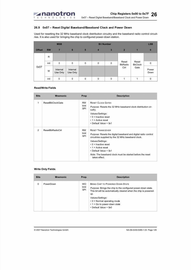
8/20/2019 nanoLOC NA5TR1 UserGuide
http://slidepdf.com/reader/full/nanoloc-na5tr1-userguide 145/325
Chip Registers 0x00 to 0x7F
0x07 – Reset Digital Baseband/Baseband Clock and Power Down
© 2007 Nanotron Technologies GmbH. NA-06-0230-0385-1.03 Page 129
26
26.9 0x07 – Reset Digital Baseband/Baseband Clock and Power Down
Used for resetting the 32 MHz baseband clock distribution circuitry and the baseband radio control circuit-
ries. It is also used for bringing the chip to configured power-down station.
Read/Write Fields
Write Only Fields
MSB Bit Number LSB
Offset RW 7 6 5 4 3 2 1 0
0x07
R
Reset
BbRadio
Ctrl
Reset
BbClock
Gate
init 0 0 0 0 0 0
WInternal
Use Only
Internal
Use Only
Power
Down
init 0 0 0 0 0 1 1 0
Bits Mnemonic Prop Description
1 ResetBbClockGate RW
brst
SPI
RESET CLOCK G ATES
Purpose: Resets the 32 MHz baseband clock distribution cir-
cuitry.
Values/Settings:
• 0 = Inactive reset
• 1 = Active reset
• Default Value = 0x1
2 ResetBbRadioCtrl RW
brst
SPI
RESET TRANSCEIVER
Purpose: Resets the digital baseband and digital radio control
circuitries supplied by the 32 MHz baseband clock.
Values/Settings:
• 0 = Inactive reset
• 1 = Active reset
• Default Value = 0x1
Note: The baseband clock must be started before the reset
takes effect.
Bits Mnemonic Prop. Description
0 PowerDown WO
brst
SPI
BRING CHIP TO POWERED DOWN STATE
Purpose: Brings the chip to the configured power-down state.
This bit will be automatically cleared when the chip is powered-
up.
Values/Settings:
• 0 = Normal operating mode
• 1 = Go to power-down state
• Default Value = 0x0

8/20/2019 nanoLOC NA5TR1 UserGuide
http://slidepdf.com/reader/full/nanoloc-na5tr1-userguide 146/325
Chip Registers 0x00 to 0x7F
0x08 – Power On/Off Baseband Crystal and Clock
Page 130 NA-06-0230-0385-1.03 © 2007 Nanotron Technologies GmbH.
26
26.10 0x08 – Power On/Off Baseband Crystal and Clock
Used for selection an optional external oscillator on pad Xtal32MP, the baseband clock distribution, and the
internal baseband quartz oscillator. It is also used for enabling and setting the feature clock frequency.
Read/Write Fields
MSB Bit Number LSB
Offset RW 7 6 5 4 3 2 1 0
0x08RW
Enable
Feature
Clock
FeatureClockFreq
Bypass
Bb
Crystal
Enable
BbClock
Enable
BbCrystal
init 0 0 0 0 0 0 0 0
Bits Mnemonic Prop Description
0 EnableBbCrystal RW
SPI
ENABLE B ASEBAND CRYSTAL
Purpose: Powers on the internal baseband quartz oscillator.
Values/Settings:
• 0 = Power off
• 1 = Power on
• Default Value = 0x0
Note: Never switch on the internal oscillator when the external
oscillator is connected to pad Xtal32MP.
1 EnableBbClock RW
SPI
ENABLE B ASEBAND CLOCK
Purpose: Enables the baseband clock distribution.Values/Settings:
• 0 = Distribution off
• 1 = Distribution on
• Default Value = 0x0
3 BypassBbCrystal RW
SPI
BYPASS B ASEBAND CRYSTAL
Purpose: Switches off the internal Oscillator when an external
oscillator is connected to pad Xtal32MP.
Values/Settings:
• 0 = Disable
• 1 = Enable
• Default Value = 0x0

8/20/2019 nanoLOC NA5TR1 UserGuide
http://slidepdf.com/reader/full/nanoloc-na5tr1-userguide 147/325
Chip Registers 0x00 to 0x7F
0x08 – Power On/Off Baseband Crystal and Clock
© 2007 Nanotron Technologies GmbH. NA-06-0230-0385-1.03 Page 131
26
4- 6 FeatureClockFreq RW
brst
SPI
FEATURE CLOCK FREQUENCY
Purpose: Sets the feature clock frequency. The feature clock
can be routed to one or more digital IO pads. The frequency ofthe Feature Clock is calculated by using the 32/2 MHz baseband
clock divided by the setting made here.
Values/Settings:
• NA_FeatureClockDiv1_C (16 MHz) (0x7)
• NA_FeatureClockDiv2_C (8 MHz) (0x6)
• NA_FeatureClockDiv4_C (4 MHz) (0x5)
• NA_FeatureClockDiv8_C (2 MHz) (0x4)
• NA_FeatureClockDiv16_C (1 MHz) (0x3)
• NA_FeatureClockDiv32_C (500 kHz) (0x2)
• NA_FeatureClockDiv64_C (250 kHz) (0x1)
• NA_FeatureClockDiv128_C (125 kHz) (0x0)
• Default Value = 0x0
Note: Change the frequency only when the feature clock is dis-abled (EnableFeatureClock = 0).
7 EnableFeatureClock RW
brst
SPI
ENABLE FEATURE CLOCK
Purpose: Enables the Feature Clock which guarantees clip and
glitch free clock waveforms on a digital IO output.
Values/Settings:
• 0 = Disable
If the Feature Clock is disabled but a digital IO pin is enabled
as clock output, the frequency is equal to the Real Time Clock
crystal frequency of 32.768 kHz.
• 1 = Enable
If enabled, the frequency depends on the value set in
FeatureClockFreq (see above).
Bits Mnemonic Prop Description

8/20/2019 nanoLOC NA5TR1 UserGuide
http://slidepdf.com/reader/full/nanoloc-na5tr1-userguide 148/325
Chip Registers 0x00 to 0x7F
0x09 – Setting SPI Pads as Pullup or Pulldown
Page 132 NA-06-0230-0385-1.03 © 2007 Nanotron Technologies GmbH.
26
26.11 0x09 – Setting SPI Pads as Pullup or Pulldown
Used for connecting pull-up and pull-down resistors to the four SPI pads: Spiclk, Spissn, Spirxd, and Spitxd.
The values programmed here are applied to the pad when they are written to the corresponding registers
through register 0x0B (see 26.13. 0x0B – Writing Pullup/Pulldown Settings to Pads on page 136). The resis-
tors are kept during power-down state.
Write Only Fields
MSB Bit Number LSB
Offset RW 7 6 5 4 3 2 1 0
0x09
R
init 0 0 0 0 0 0 0 0
W
Use
Pulldown
4Spitxd
Use
Pullup
4Spitxd
Use
Pulldown
4Spirxd
Use
Pullup
4Spirxd
Use
Pulldown
4Spissn
Use
Pullup
4Spissn
Use
Pulldown
4Spiclk
Use
Pullup
4Spiclk
init 0 0 0 0 0 0 0 0
Bits Mnemonic Prop Description
0 UsePullup4Spiclk WO
brst
SPI
CONNECT A PULL-UP RESISTOR TO SPI CLOCK P AD
Purpose: When this bit is set to 1, a pull-up resistor is connected
to the SPI clock pad.
Values/Settings:
• 0 = No pull-up resistor
• 1 = Use pull-up resistor
• Default Value = 0x0
1 UsePulldown4Spiclk WO
brst
SPI
CONNECT A PULL-DOWN RESISTOR TO SPI CLOCK P AD
Purpose: When this bit is set to 1, a pull-down resistor is con-
nected to the SPI clock pad, but only when UsePullup4Spiclk is
0.
Values/Settings:
• 0 = No pull-down resistor
• 1 = Use pull-down resistor
• Default Value = 0x0
2 UsePullup4Spissn WO
brst
SPI
CONNECT A PULL-UP RESISTOR TO SPI SSN P AD
Purpose: When this bit is set to 1, a pull-up resistor is connected
to the SPI Ssn pad.
Values/Settings:
• 0 = No pull-up resistor
• 1 = Use pull-up resistor
• Default Value = 0x0

8/20/2019 nanoLOC NA5TR1 UserGuide
http://slidepdf.com/reader/full/nanoloc-na5tr1-userguide 149/325
Chip Registers 0x00 to 0x7F
0x09 – Setting SPI Pads as Pullup or Pulldown
© 2007 Nanotron Technologies GmbH. NA-06-0230-0385-1.03 Page 133
26
3 UsePulldown4Spissn WO
brst
SPI
CONNECT A PULL-DOWN RESISTOR TO SPI SSN P AD
Purpose: When this bit is set to 1, a pull-down resistor is con-
nected to the SPI Ssn pad, but only when UsePullup4Spissn is0.
Values/Settings:
• 0 = No pull-down resistor
• 1 = Use pull-down resistor
• Default Value = 0x0
4 UsePullup4Spirxd WO
brst
SPI
CONNECT A PULL-UP RESISTOR TO SPI RXD P AD
Purpose: When this bit is set to 1, a resistor is connected to the
SPI RxD Pad.
Values/Settings:
• 0 = No pull-up resistor
• 1 = Use pull-up resistor
• Default Value = 0x0
5 UsePulldown4Spirxd WO
brst
SPI
CONNECT A PULL-DOWN RESISTOR TO SPI RXD P AD
Purpose: When this bit is set to 1, a pull-down resistor is con-
nected to the SPI RxD pad, but only when UsePullup4Spirxd is
0.
Values/Settings:
• 0 = No pull-down resistor
• 1 = Use pull-down resistor
• Default Value = 0x0
6 UsePullup4Spitxd WO
brstSPI
CONNECT A PULL-UP RESISTOR TO SPI TXD P AD
Purpose: When this bit is set to 1, a resistor is connected to theSPI TxD Pad.
Values/Settings:
• 0 = No pull-up resistor
• 1 = Use pull-up resistor
• Default Value = 0x0
7 UsePulldown4Spitxd WO
brst
SPI
CONNECT A PULL-DOWN RESISTOR TO SPI TXD P AD
Purpose: When this bit is set to 1, a pull-down resistor is con-
nected to the SPI TxD pad, but only when UsePullup4Spitxd is
0.
Values/Settings:
• 0 = No pull-down resistor
• 1 = Use pull-down resistor
• Default Value = 0x0
Bits Mnemonic Prop Description

8/20/2019 nanoLOC NA5TR1 UserGuide
http://slidepdf.com/reader/full/nanoloc-na5tr1-userguide 150/325
Chip Registers 0x00 to 0x7F
0x0A – Setting Additional Pads as Pullup or Pulldown
Page 134 NA-06-0230-0385-1.03 © 2007 Nanotron Technologies GmbH.
26
26.12 0x0A – Setting Additional Pads as Pullup or Pulldown
Used for connecting the pull-up or the pull-down resistors to the four pads: /POnReset, Pamp, µCIrq, and
µCReset. The values programmed here are applied to the pad when they are written to the corresponding
registers through register 0x0B (see 26.13. 0x0B – Writing Pullup/Pulldown Settings to Pads on page 136).
The resistors are kept during power-down state.
Write Only Fields
MSB Bit Number LSB
Offset RW 7 6 5 4 3 2 1 0
0x0A
R
init 0 0 0 0 0 0 0 0
W
Use
Pulldown
4Ucrst
Use
Pullup
4Ucrst
Use
Pulldown
4Ucirq
Use
Pullup
4Ucirq
Use
Pulldown
4Pamp
Use
Pullup
4Pamp
Use
Pulldown
4Por
Use
Pullup
4Por
init 0 0 0 0 0 0 0 0
Bits Mnemonic Prop Description
0 UsePullup4Por WO
brst
SPI
CONNECT A PULL-UP RESISTOR TO POR P AD
Purpose: When this bit is set to 1, a pull-up resistor is connected
to the POR pad.
Values/Settings:
• 0 = No pull-up resistor
• 1 = Use pull-up resistor
• Default Value = 0x0
1 UsePulldown4Por WO
brst
SPI
CONNECT A PULL-DOWN RESISTOR TO POR P AD
Purpose: When this bit is set to 1, a pull-down resistor is con-
nected to the POR pad, but only when UsePullup4Por is 0.
Values/Settings:
• 0 = No pull-down resistor
• 1 = Use pull-down resistor
• Default Value = 0x0
2 UsePullup4Pamp WO
brst
SPI
CONNECT A PULL-UP RESISTOR TO PAMP P AD
Purpose: When this bit is set to 1, a pull-up resistor is connectedto the PAMP pad.
Values/Settings:
• 0 = No pull-up resistor
• 1 = Use pull-up resistor
• Default Value = 0x0
3 UsePulldown4Pamp WO
brst
SPI
CONNECT A PULL-DOWN RESISTOR TO PAMP P AD
Purpose: When this bit is set to 1, a pull-down resistor is con-
nected to the PAMP pad, but only when UsePullup4Pamp is 0.
Values/Settings:
• 0 = No pull-down resistor
• 1 = Use pull-down resistor
• Default Value = 0x0

8/20/2019 nanoLOC NA5TR1 UserGuide
http://slidepdf.com/reader/full/nanoloc-na5tr1-userguide 151/325
Chip Registers 0x00 to 0x7F
0x0A – Setting Additional Pads as Pullup or Pulldown
© 2007 Nanotron Technologies GmbH. NA-06-0230-0385-1.03 Page 135
26
4 UsePullup4Ucirq WO
brst
SPI
CONNECT A PULL-UP RESISTOR TO UCIRQ P AD
Purpose: When this bit is set to 1, a pull-up resistor is connected
to the ucIRQ pad.
Values/Settings:
• 0 = No pull-up resistor
• 1 = Use pull-up resistor
• Default Value = 0x0
5 UsePulldown4Ucirq WO
brst
SPI
CONNECT A PULL-DOWN RESISTOR TO UCIRQ P AD
Purpose: When this bit is set to 1, a pull-down resistor is con-
nected to the ucIRQ pad, but only when UsePullup4Ucirq is 0.
Values/Settings:
• 0 = No pull-down resistor
• 1 = Use pull-down resistor
• Default Value = 0x0
6 UsePullup4Ucrst WO
brst
SPI
CONNECT A PULL-UP RESISTOR TO UCRST P AD
Purpose: When this bit is set to 1, a pull-up resistor is connected
to the ucRST pad.
Values/Settings:
• 0 = No pull-up resistor
• 1 = Use pull-up resistor
• Default Value = 0x0
7 UsePulldown4Ucrst WO
brst
SPI
CONNECT A PULL-DOWN RESISTOR TO UCRST P AD
Purpose: When this bit is set to 1, a pull-up resistor is connected
to the ucRST pad, but only when UsePullup4Ucrst is 0.
Values/Settings:
• 0 = No pull-down resistor
• 1 = Use pull-down resistor
• Default Value = 0x0
Bits Mnemonic Prop Description

8/20/2019 nanoLOC NA5TR1 UserGuide
http://slidepdf.com/reader/full/nanoloc-na5tr1-userguide 152/325
Chip Registers 0x00 to 0x7F
0x0B – Writing Pullup/Pulldown Settings to Pads
Page 136 NA-06-0230-0385-1.03 © 2007 Nanotron Technologies GmbH.
26
26.13 0x0B – Writing Pullup/Pulldown Settings to Pads
Used for writing the settings made in registers 0x09 and/or 0x0A to the appropriate pads on the chip.
Because the destination registers are running with the 32.768 kHz clock, the write strobe has to be active
for at least 30.6 ms.
Note: A write strobe must always be generated by programming a 1-0-sequence to this register. Do NOT
change the content of registers 0x09 (see 26.11. 0x09 – Setting SPI Pads as Pullup or Pulldown on
page 132) and 0x0A (see 26.12. 0x0A – Setting Additional Pads as Pullup or Pulldown on page 134)
when one of the bits of this register is active.
Write Only Fields
MSB Bit Number LSB
Offset RW 7 6 5 4 3 2 1 0
0x0B
R
init 0 0 0 0 0 0 0 0
W
Write
Pulls
4Pads
Write
Pulls
4Spi
init 0 0 0 0 0 0 0 0
Bits Mnemonic Prop Description
0 WritePulls4Spi WO
brst
SPI
WRITE PULL-UP AND PULL-DOWN SETTINGS TO FOUR SPI P ADS
Purpose: Writes the SPI pad settings (see register 0x9) to the
appropriate chip pads.
Purpose:
• 0 = True
• 1 = False
• Default Value = 0x0
1 WritePulls4Pads WO
brst
SPI
WRITE PULL-UP AND PULL-DOWN SETTINGS TO FOUR
ADDITIONAL P ADS
Purpose: Writes the additional pad settings (see register 0xA) to
the appropriate chip pads.
Purpose:
• 0 = True
• 1 = False
• Default Value = 0x0

8/20/2019 nanoLOC NA5TR1 UserGuide
http://slidepdf.com/reader/full/nanoloc-na5tr1-userguide 153/325
Chip Registers 0x00 to 0x7F
0x0C – Internal Use Only
© 2007 Nanotron Technologies GmbH. NA-06-0230-0385-1.03 Page 137
26
26.14 0x0C – Internal Use Only
Nanotron internal use only. During normal operations, this register must be set to “0”.
MSB Bit Number LSB
Offset RW 7 6 5 4 3 2 1 0
0x0CRW Internal Use Only
init 0 0 0 0 0 0 0 0

8/20/2019 nanoLOC NA5TR1 UserGuide
http://slidepdf.com/reader/full/nanoloc-na5tr1-userguide 154/325
Chip Registers 0x00 to 0x7F
0x0D – Internal Use Only
Page 138 NA-06-0230-0385-1.03 © 2007 Nanotron Technologies GmbH.
26
26.15 0x0D – Internal Use Only
Nanotron internal use only. During normal operations, this register must be set to “0”.
MSB Bit Number LSB
Offset RW 7 6 5 4 3 2 1 0
0x0DRW Internal Use Only
init 0 0 0 0 0 0 0 0

8/20/2019 nanoLOC NA5TR1 UserGuide
http://slidepdf.com/reader/full/nanoloc-na5tr1-userguide 155/325
Chip Registers 0x00 to 0x7F
0x0E – Baseband Memory Access
© 2007 Nanotron Technologies GmbH. NA-06-0230-0385-1.03 Page 139
26
26.16 0x0E – Baseband Memory Access
Used together to selecting pages of the baseband RAM, the correlator memory, or the chirp sequencer
RAM, which are then mapped into the Device Window.
Note: See also 8.1. Selecting a Memory Address on page 40.
Read/Write Fields
MSB Bit Number LSB
Offset RW 7 6 5 4 3 2 1 0
0x0ERW DeviceSelect RamIndex
init 0 0 0 0 0 0 0 0
Bits Mnemonic Prop. Description
0-1 RamIndex RW
brst
SPI
SELECT P AGE IN B ASEBAND MEMORY
Purpose: Selects one page of selected memory type (see
DeviceSelect below) to be mapped into accessible SPI address
space. When addresses are greater than 0xFF, the higher bits
have to be written to this field.
Values/Settings:
• To select a baseband RAM page, select one of:
• Baseband RAM block 0 (0x0)
• Baseband RAM block 1 (0x1)
• Baseband RAM block 2 (0x2)
• Baseband RAM block 3 (0x3)
• To select a chirp sequencer (CSQ) RAM column, select one of:• Column 0 (0x0)
• Column 1 (0x1)
• Column 2 (0x2)
• Unused (0x3)
• For correlator memory, select one of:
• I (RamD3IPatI) (0x0)
• Q (RamD3IPatQ) (0x1)
• Thresholds (RamD3IThresholds) (0x2)
• Unused (0x3)
• Default Value = 0x0
Note: Register access to locations < 0x80 are not influenced by
index settings.
4-5 DeviceSelect RW
brst
SPI
SELECT MEMORY TYPE
Purpose: Selects either the baseband RAM, the chirp sequencer
RAM or the correlator memory to be mapped into the accessible
SPI address space
Values/Settings:
• For baseband RAM, select:
• NA_DeviceSelectBbRam0_C(0x0)
• Unused(0x1)
• For chirp sequencer RAM, select:
• NA_DeviceSelectCsq_C(0x2)
• For correlator memory, select:
• NA_DeviceSelectD3l_C(0x3)
• Default Value = 0x0
Note: Register access to memory locations less than 0x80 are
not influenced by index settings.

8/20/2019 nanoLOC NA5TR1 UserGuide
http://slidepdf.com/reader/full/nanoloc-na5tr1-userguide 156/325
Chip Registers 0x00 to 0x7F
0x0F – LO, BBTimer, RX/TX IRQ Event Status and Enabling
Page 140 NA-06-0230-0385-1.03 © 2007 Nanotron Technologies GmbH.
26
26.17 0x0F – LO, BBTimer, RX/TX IRQ Event Status and Enabling
Used for selecting sources (LO, baseband timer, receiver, transmitter) that drive an external interrupt when
an event occurs. It is also used for reporting the occurance of an interrupt event for one of the enabled
receive/transmit interrupts.
Note: The status bits in 4 to 7 are independent of the enable bits 0 to 3.
Read/Write Fields
MSB Bit Number LSB
Offset RW 7 6 5 4 3 2 1 0
0x0F
RLoIrq
Status
BbTimer
IrqStatus
RxIrq
Status
TxIrq
StatusLoIrq
Enable
BbTimer
Irq
Enable
RxIrq
Enable
TxIrq
Enableinit 0 0 0 0
W
init 0 0 0 0 0 0 0 0
Bits Mnemonic Prop Description
0 TxIrqEnable RW
brst
SPI
ENABLE TRANSMITTER INTERRUPT
Values/Settings:
• 0 = Disable
TX interrupt does not drive the interrupt line.
• 1 = Enable
TX interrupt drives the interrupt line.
• Default Value = 0x0
1 RxIrqEnable RW
brst
SPI
ENABLE RECEIVER INTERRUPT
Values/Settings:
• 0 = Disable
RX interrupt does not drive the interrupt line.
• 1 = Enable
RX interrupt drives the interrupt line.
• Default Value = 0x0
2 BbTimerIrqEnable RW
brst
SPI
ENABLE B ASEBAND TIMER INTERRUPT
Values/Settings:
• 0 = Disable
BbTimer interrupt does not drive the interrupt line.
• 1 = Enable
BbTimer interrupt drives the interrupt line.
• Default Value = 0x0
3 LoIrqEnable RW
brst
SPI
ENABLE LO INTERRUPT
Values/Settings:
• 0 = Disable
LO interrupt does not drive the interrupt line.
• 1 = Enable
LO interrupt drives the interrupt line.
• Default Value = 0x0

8/20/2019 nanoLOC NA5TR1 UserGuide
http://slidepdf.com/reader/full/nanoloc-na5tr1-userguide 157/325
Chip Registers 0x00 to 0x7F
0x0F – LO, BBTimer, RX/TX IRQ Event Status and Enabling
© 2007 Nanotron Technologies GmbH. NA-06-0230-0385-1.03 Page 141
26
Read Only Fields
Bits Mnemonic Prop Description
4 TxIrqStatus RO TRANSMITTER INTERRUPT EVENT STATUS
Purpose: Reports the occurance of one or more of the enabled
transmitter interrupts.
Values/Settings:
• 0 = Event did not trigger
This bit is cleared when an enabled (via register 0x13) trans-
mitter interrupt is either cleared via register 0x10 or disabled
via register 0x13.
• 1 = Event is triggered
This bit is 1 when one or more of the enabled (via register
0x13) transmitter interrupts have occurred. Their raw status is
reported in register 0x10.
• Default Value = 0x0
5 RxIrqStatus RO RECEIVER INTERRUPT EVENT STATUS
Purpose: Reports the occurance of one or more of the enabled
receiver interrupts.
Values/Settings:
• 0 = Event did not trigger
This bit is cleared when an enabled (via register 0x14) receiver
interrupt is either cleared via register 0x11 or disabled via reg-
ister 0x14.
• 1 = Event is triggered
This bit is 1 when one or more of the enabled (via register
0x14) receiver interrupts have occurred. Their raw status is
reported in register 0x11.
• Default Value = 0x0
6 BbTimerIrqStatus RO B ASEBAND TIMER EVENT STATUS
Purpose: Reports the occurance of a baseband timer event.
Values/Settings:
• 0 = Event did not trigger
This bit is cleared when the BBTimer interrupt is reset via the
register 0x12.
• 1 = Event is triggered
This bit is 1 when the baseband timer has reached its end.
• Default Value = 0x0
7 LoIrqStatus RO LO IRQ EVENT STATUS
Purpose: Reports the occurance of a LO IRQ event.
Values/Settings:
• 0 = Event did not trigger
This bit is cleared when an enabled (via register 0x15) LO
interrupt is either cleared via register 0x12 (WARNING: one of
the sources is state triggered) or disabled via register 0x15.
• 1 = Event is triggered
This bit is 1 when one or more of the enabled (via register
0x15) LO interrupts haVE occurred. Their raw status is
reported in register 0x12.
• Default Value = 0x0

8/20/2019 nanoLOC NA5TR1 UserGuide
http://slidepdf.com/reader/full/nanoloc-na5tr1-userguide 158/325
Chip Registers 0x00 to 0x7F
0x10 – TX Raw Interrupt Status and Reset [Index]
Page 142 NA-06-0230-0385-1.03 © 2007 Nanotron Technologies GmbH.
26
26.18 0x10 – TX Raw Interrupt Status and Reset [Index]
Used for reporting the TX raw interrupt status of the transmitter and for clearing the interrupt status of the
corresponding source.
Read Only Fields
Write Only Fields
MSB Bit Number LSB
Offset RW 7 6 5 4 3 2 1 0
0x10
R TxIntsRawStat
init 0 0 0 0 0 0 0 0
W TxIntsReset
init 0 0 0 0 0 0 0 0
Bits Mnemonic Prop Description
0-5 TxIntsRawStat RO
brst
BbClk
TRANSMITTER INTERRUPT R AW STATUS
Purpose: Reports the TX raw interrupt of each source.
Values/Settings:
• See Bit Offsets (Indexes) section below.
Bits Mnemonic Prop Description
0-5 TxIntsReset WO
brst
strb
BbClk
TRANSMITTER INTERRUPT RESET
Purpose: Clears the interrupt status of the
corresponding source.
Values/Settings:
• See Bit Offsets (Indexes) section below.
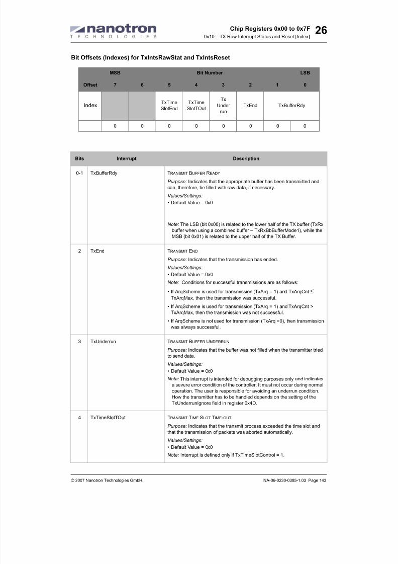
8/20/2019 nanoLOC NA5TR1 UserGuide
http://slidepdf.com/reader/full/nanoloc-na5tr1-userguide 159/325
Chip Registers 0x00 to 0x7F
0x10 – TX Raw Interrupt Status and Reset [Index]
© 2007 Nanotron Technologies GmbH. NA-06-0230-0385-1.03 Page 143
26
Bit Offsets (Indexes) for TxIntsRawStat and TxIntsReset
MSB Bit Number LSB
Offset 7 6 5 4 3 2 1 0
IndexTxTime
SlotEnd
TxTime
SlotTOut
Tx
Under
run
TxEnd TxBufferRdy
0 0 0 0 0 0 0 0
Bits Interrupt Description
0-1 TxBufferRdy TRANSMIT BUFFER READY
Purpose: Indicates that the appropriate buffer has been transmitted and
can, therefore, be filled with raw data, if necessary.
Values/Settings:
• Default Value = 0x0
Note: The LSB (bit 0x00) is related to the lower half of the TX buffer (TxRx
buffer when using a combined buffer – TxRxBbBufferMode1), while the
MSB (bit 0x01) is related to the upper half of the TX Buffer.
2 TxEnd TRANSMIT END
Purpose: Indicates that the transmission has ended.
Values/Settings:• Default Value = 0x0
Note: Conditions for successful transmissions are as follows:
• If ArqScheme is used for transmission (TxArq = 1) and TxArqCnt ≤
TxArqMax, then the transmission was successful.
• If ArqScheme is used for transmission (TxArq = 1) and TxArqCnt >
TxArqMax, then the transmission was not successful.
• If ArqScheme is not used for transmission (TxArq =0), then transmission
was always successful.
3 TxUnderrun TRANSMIT BUFFER UNDERRUN
Purpose: Indicates that the buffer was not filled when the transmitter tried
to send data.
Values/Settings:
• Default Value = 0x0
Note: This interrupt is intended for debugging purposes only and indicates
a severe error condition of the controller. It must not occur during normal
operation. The user is responsible for avoiding an underrun condition.
How the transmitter has to be handled depends on the setting of the
TxUnderrunIgnore field in register 0x4D.
4 TxTimeSlotTOut TRANSMIT TIME SLOT TIME-OUT
Purpose: Indicates that the transmit process exceeded the time slot and
that the transmission of packets was aborted automatically.
Values/Settings:
• Default Value = 0x0Note: Interrupt is defined only if TxTimeSlotControl = 1.

8/20/2019 nanoLOC NA5TR1 UserGuide
http://slidepdf.com/reader/full/nanoloc-na5tr1-userguide 160/325
Chip Registers 0x00 to 0x7F
0x10 – TX Raw Interrupt Status and Reset [Index]
Page 144 NA-06-0230-0385-1.03 © 2007 Nanotron Technologies GmbH.
26
5 TxTimeSlotEnd TRANSMIT TIME SLOT END
Purpose: Indicates that the transmit time slot has ended.
Values/Settings:
• Default Value = 0x0
Note: Interrupt is defined only if TxTimeSlotControl = 1.
Bits Interrupt Description

8/20/2019 nanoLOC NA5TR1 UserGuide
http://slidepdf.com/reader/full/nanoloc-na5tr1-userguide 161/325
Chip Registers 0x00 to 0x7F
0x11 – RX Raw Interrupt Status and Reset [Index]
© 2007 Nanotron Technologies GmbH. NA-06-0230-0385-1.03 Page 145
26
26.19 0x11 – RX Raw Interrupt Status and Reset [Index]
Used for reporting the RX raw interrupt status of the receiver and for clearing the interrupt status of the cor-
responding source.
Read Only Fields
Write Only Fields
MSB Bit Number LSB
Offset RW 7 6 5 4 3 2 1 0
0x11
R RxIntsRawStat
init 0 0 0 0 0 0 0 0
W RxIntsReset
init 0 0 0 0 0 0 0 0
Bits Mnemonic Prop Description
0-6 RxIntsRawStat RO
brst
BbClk
RECEIVER INTERRUPT R AW STATUS
Purpose: Reports the RX raw interrupt of each source.
Values/Settings:
• See Bit Offsets (Indexes) section below.
Bits Mnemonic Prop Description
0-6 RxIntsReset WO
brst
strb
BbClk
Reset Receiver Interrupt
Purpose: Clears the interrupt status of the corresponding
source.
Values/Settings:
• See Bit Offsets (Indexes) section below.

8/20/2019 nanoLOC NA5TR1 UserGuide
http://slidepdf.com/reader/full/nanoloc-na5tr1-userguide 162/325
Chip Registers 0x00 to 0x7F
0x11 – RX Raw Interrupt Status and Reset [Index]
Page 146 NA-06-0230-0385-1.03 © 2007 Nanotron Technologies GmbH.
26
Bit Offsets (Indexes) for RxIntsRawStat and RxIntsReset
MSB Bit Number LSB
Offset 7 6 5 4 3 2 1 0
IndexRxTime
SlotEnd
RxTime
SlotTOut
RxOver-
flow
Rx
Header
End
RxEnd RxBufferRdy
0 0 0 0 0 0 0 0
Bits Interrupt Description
1-0 RxBufferRdy RECEIVE BUFFER READY
Purpose: Indicates that the appropriate receive buffer is filled with data
and can be read out.
Values/Settings:
• Default Value = 0x0
Note: The LSB (0x00) is related to the lower half of the RX buffer (TxRx
buffer when using a combined buffer – TxRxBbBufferMode1), while the
MSB (0x01) is related to the upper half of the RX buffer.
2 RxEnd END OF P ACKET RECEPTION
Purpose: Indicates that end of a correct packet was detected.
Values/Settings:
• Default Value = 0x0
Note: This interrupt depends on the settings of RxCrc2Mode field andRxArqMode field in register 0x5A.
3 RxHeaderEnd END OF CORRECT HEADER RECEPTION
Purpose: Indicates the reception of a correct header.
Values/Settings:
• Default Value = 0x0
Note: Only usable in auto mode.
4 RxOverflow RECEIVE BUFFER OVERFLOW
Purpose: Indicates that the receiver was not able to place data in the RX
buffer because the RX buffer was full. No RxEnd interrupt is generated
and no Ack packet will be transmitted
Values/Settings:
• Default Value = 0x0
• This interrupt is intended for debugging purposes only and indicates
an error condition of the controller. It should not occur during normal
operation. The user is responsible to avoid the overflow condition.
• This interrupt must be ignored when RxCrc2Mode field in register
0x5A is set to 1.
• Before a reception can be restarted through the
RxCmdStart command, the pending RxBufferRdy interrupts and the
receive buffers (through RxBufferCmd) must be cleared.
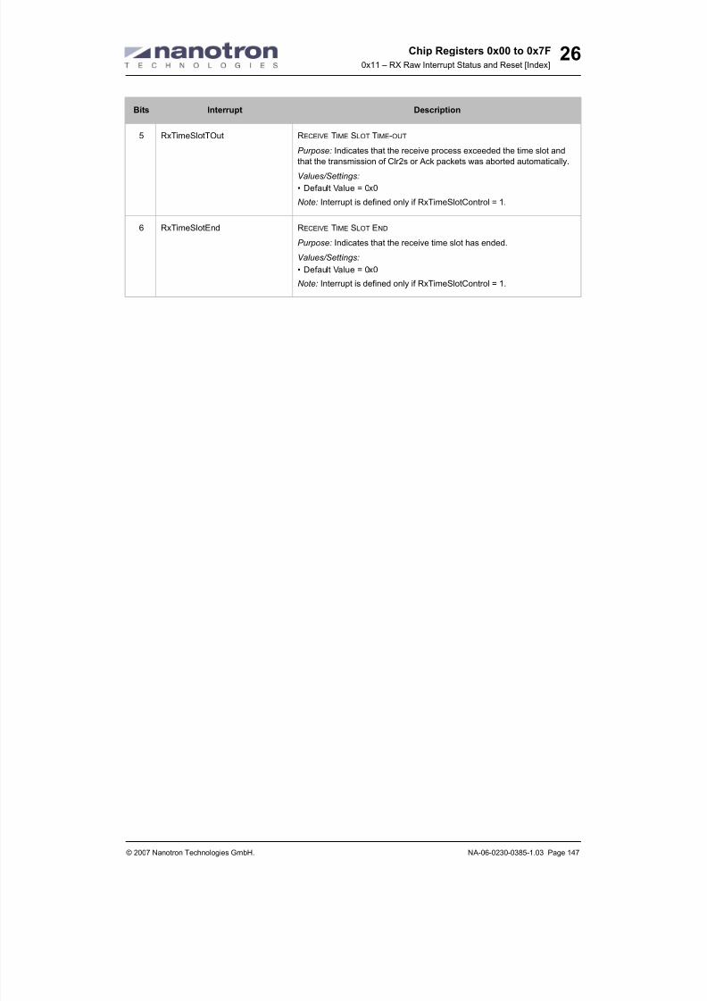
8/20/2019 nanoLOC NA5TR1 UserGuide
http://slidepdf.com/reader/full/nanoloc-na5tr1-userguide 163/325
Chip Registers 0x00 to 0x7F
0x11 – RX Raw Interrupt Status and Reset [Index]
© 2007 Nanotron Technologies GmbH. NA-06-0230-0385-1.03 Page 147
26
5 RxTimeSlotTOut RECEIVE TIME SLOT TIME-OUT
Purpose: Indicates that the receive process exceeded the time slot and
that the transmission of Clr2s or Ack packets was aborted automatically.
Values/Settings:
• Default Value = 0x0
Note: Interrupt is defined only if RxTimeSlotControl = 1.
6 RxTimeSlotEnd RECEIVE TIME SLOT END
Purpose: Indicates that the receive time slot has ended.
Values/Settings:
• Default Value = 0x0
Note: Interrupt is defined only if RxTimeSlotControl = 1.
Bits Interrupt Description

8/20/2019 nanoLOC NA5TR1 UserGuide
http://slidepdf.com/reader/full/nanoloc-na5tr1-userguide 164/325
Chip Registers 0x00 to 0x7F
0x12 – LO and BBTimer Raw Interrupt Status and Reset [Index]
Page 148 NA-06-0230-0385-1.03 © 2007 Nanotron Technologies GmbH.
26
26.20 0x12 – LO and BBTimer Raw Interrupt Status and Reset [Index]
Used for storing the LO interrupt of a triggered event and for clearing the interrupt status of the correspond-
ing source. It is also used for resetting the baseband timer interrupt or for stopping the baseband timer.
Read Only Fields
Write Only Fields
MSB Bit Number LSB
Offset RW 7 6 5 4 3 2 1 0
0x12
RLoInts
RawStat
Internal
Use Only
init 0 0 0 0 0 0 0 0
W
Clear
Base
band
Timer
Int
LoInts
Reset
Internal
Use Only
init 0 0 0 0 0 0 0 0
Bits Mnemonic Prop Description
1 LoIntsRawStat RO
brst
BbClk
LOCAL OSCILLATOR INTERRUPT R AW STATUS
Purpose: Stores the LO interrupt of a triggered event.
Values/Settings:
• See Bit Offsets (Indexes) section below.
Bits Mnemonic Prop Description
1 LoIntsReset WO
brst
strb
BbClk
Reset Local Oscillator interrupt
Purpose: Clears the interrupt status of the
corresponding source.
Values/Settings:
• See Bit Offsets (Indexes) section below.
7 ClearBasebandTimerInt WO
brst
strb
BbClk
B ASEBAND TIMER INTERRUPT RESET
Purpose: Clears the BbTimer interrupt or stops the timer, if it
has not reached zero.
Values/Settings:
• Default Value = 0x0
Note: After ClearBasebandTimerInt, the timer can be restarted
again.

8/20/2019 nanoLOC NA5TR1 UserGuide
http://slidepdf.com/reader/full/nanoloc-na5tr1-userguide 165/325

8/20/2019 nanoLOC NA5TR1 UserGuide
http://slidepdf.com/reader/full/nanoloc-na5tr1-userguide 166/325
Chip Registers 0x00 to 0x7F
0x13 – Enable Transmitter Interrupts [Index]
Page 150 NA-06-0230-0385-1.03 © 2007 Nanotron Technologies GmbH.
26
26.21 0x13 – Enable Transmitter Interrupts [Index]
Used for enabling the different transmitter interrupt sources to control TxIrqStatus in register 0x0F (see
26.17. 0x0F – LO, BBTimer, RX/TX IRQ Event Status and Enabling on page 140).
Write Only Fields
Bit Offsets (Indexes) for TxIntsEn
MSB Bit Number LSB
Offset RW 7 6 5 4 3 2 1 0
0x13
R
init 0 0 0 0 0 0 0 0
W TxIntsEn
init 0 0 0 0 0 0 0 0
Bits Mnemonic Prop Description
0-5 TxIntsEn WO
brst
BbClk
ENABLE TRANSMITTER INTERRUPT
Purpose: Enables the different TX interrupt sources to control
TxIrqStatus.
Values/Settings:
• See Bit Offsets (Indexes) section below.
MSB Bit Number LSB
Offset 7 6 5 4 3 2 1 0
IndexTxTime
SlotEnd
TxTime
SlotTOut
Tx
Under
run
TxEnd TxBufferRdy
0 0 0 0 0 0 0 0
Bits Interrupt Description
0-1 TxBufferRdy TRANSMIT BUFFER READY
Purpose: Indicates that the appropriate buffer has been transmitted and
can be filled with data.
Values/Settings:
• Default Value = 0x0
Note: The LSB (bit 0x00) is related to the lower half of the TX buffer (TxRx
buffer when using a combined buffer – TxRxBbBufferMode1), while the
MSB (bit 0x01) is related to the upper half of the TX buffer.

8/20/2019 nanoLOC NA5TR1 UserGuide
http://slidepdf.com/reader/full/nanoloc-na5tr1-userguide 167/325
Chip Registers 0x00 to 0x7F
0x13 – Enable Transmitter Interrupts [Index]
© 2007 Nanotron Technologies GmbH. NA-06-0230-0385-1.03 Page 151
26
2 TxEnd TRANSMIT END
Purpose: Indicates that the transmission has ended.
Values/Settings:
• Default Value = 0x0
Note: Conditions for a successful transmission are as follows:
• If ArqScheme is used for transmission (TxArq = 1) and TxArqCnt ≤ TxAr-
qMax, then the transmission was successful.
• If ArqScheme is used for transmission (TxArq = 1) and TxArqCnt > TxAr-
qMax, then the transmission was not successful.
• If ArqScheme is not used for transmission (TxArq =0) then transmission
was always successful.
3 TxUnderrun TRANSMIT BUFFER UNDERRUN
Purpose: Indicates that buffer was not filled when the transmitter tried to
send data.
Values/Settings:
• Default Value = 0x0
Note: This interrupt is intended for debugging purposes only and indicates
a severe error condition of the controller. It must not occur during normal
operation. The user is responsible for avoiding the underrun condition.
How the transmitter has to be handled depends on the setting of the
TxUnderrunIgnore field in register 0x4D.
4 TxTimeSlotTOut TRANSMIT TIME SLOT TIME-OUT
Purpose: Indicates that the transmit process exceeded the time slot and
that the transmission of packets was aborted automatically.
Values/Settings:
• Default Value = 0x0
Note: Interrupt is defined only if TxTimeSlotControl = 1.
5 TxTimeSlotEnd TRANSMIT TIME SLOT END
Purpose: Indicates that the transmit time slot has ended.
Values/Settings:
• Default Value = 0x0
Note: Interrupt is defined only if TxTimeSlotControl = 1.
Bits Interrupt Description

8/20/2019 nanoLOC NA5TR1 UserGuide
http://slidepdf.com/reader/full/nanoloc-na5tr1-userguide 168/325
Chip Registers 0x00 to 0x7F
0x14 – Receiver Interrupt Enable [Index]
Page 152 NA-06-0230-0385-1.03 © 2007 Nanotron Technologies GmbH.
26
26.22 0x14 – Receiver Interrupt Enable [Index]
Used for enabling the different receiver interrupt sources to control RxIrqStatus in register 0x0F (see 26.17.
0x0F – LO, BBTimer, RX/TX IRQ Event Status and Enabling on page 140).
Write Only Fields
Bit Offsets (Indexes) for RX Interrupts
MSB Bit Number LSB
Offset RW 7 6 5 4 3 2 1 0
0x14
R
init 0 0 0 0 0 0 0 0
W RxIntsEn
init 0 0 0 0 0 0 0 0
Bits Mnemonic Prop Description
0-6 RxIntsEn WO
brst
BbClk
ENABLE RECEIVER INTERRUPT
Purpose: Enables the different RX interrupt sources to control
the combined RxIrqStatus.
Values/Settings:
• See Bit Offsets (Indexes) section below.
MSB Bit Number LSB
Offset 7 6 5 4 3 2 1 0
IndexRxTime
SlotEnd
RxTime
SlotTOut
RxOver
flow
Rx
Header
End
RxEnd RxBufferRdy
0 0 0 0 0 0 0 0
Bits Interrupt Description
1-0 RxBufferRdy RECEIVE BUFFER READY
Purpose: Indicates that the appropriate receive buffer is filled with data
and can be read out.
Values/Settings:
• Default Value = 0x0
Note: The LSB (0x00) is related to the lower half of the RX buffer (TxRx
buffer when using a combined buffer – TxRxBbBufferMode1), while the
MSB (0x01) is related to the upper half of the RX buffer.

8/20/2019 nanoLOC NA5TR1 UserGuide
http://slidepdf.com/reader/full/nanoloc-na5tr1-userguide 169/325
Chip Registers 0x00 to 0x7F
0x14 – Receiver Interrupt Enable [Index]
© 2007 Nanotron Technologies GmbH. NA-06-0230-0385-1.03 Page 153
26
2 RxEnd END OF P ACKET RECEPTION
Purpose: Indicates that end of a correct packet was detected.
Values/Settings:
• Default Value = 0x0
Note: This interrupt depends on the settings of RxCrc2Mode field and
RxArqMode field in register 0x5A.
3 RxHeaderEnd END OF CORRECT HEADER RECEPTION
Purpose: Indicates the reception of a correct header.
Values/Settings:
• Default Value = 0x0
Note: Only usable in auto mode.
4 RxOverflow RECEIVE BUFFER OVERFLOW
Purpose: Indicates that the receiver was not able to place data in the
receive buffer because the receive buffer was full. No RxEnd interrupt is
generated and no Ack packet will be transmitted.
Values/Settings:
• Default Value = 0x0
Note: This interrupt is intended for debugging purposes only and indicates
an error condition of the controller. It should not occur during normal
operation. The user is responsible to avoid the overflow condition.
• This interrupt must be ignored when RxCrc2Mode field in register
0x5A is set to 1.
• Before a reception can be restarted through the RxCmdStart com-
mand, the pending RxBufferRdy interrupts and the receive buffers
(through RxBufferCmd) must be cleared.
5 RxTimeSlotTOut RECEIVE TIME SLOT TIME-OUT
Purpose: Indicates that the receive process exceeded the time slot and
that the transmission of Clr2s or Ack packets was aborted automatically.
Values/Settings:
• Default Value = 0x0
Note: Interrupt is defined only if RxTimeSlotControl = 1.
6 RxTimeSlotEnd RECEIVE TIME SLOT END
Purpose: Indicates that the receive time slot has ended.
Values/Settings:
• Default Value = 0x0
Note: Interrupt is defined only if RxTimeSlotControl = 1.
Bits Interrupt Description

8/20/2019 nanoLOC NA5TR1 UserGuide
http://slidepdf.com/reader/full/nanoloc-na5tr1-userguide 170/325

8/20/2019 nanoLOC NA5TR1 UserGuide
http://slidepdf.com/reader/full/nanoloc-na5tr1-userguide 171/325
Chip Registers 0x00 to 0x7F
0x16 to 0x18 – RF Local Oscillator RX Capacitors
© 2007 Nanotron Technologies GmbH. NA-06-0230-0385-1.03 Page 155
26
26.24 0x16 to 0x18 – RF Local Oscillator RX Capacitors
Used for reading the 22 switchable capacitors of the Local Oscillator after tuning as well as for setting the 22
switchable capacitors of the Local Oscillator for the RX frequencies.
Note: To save time, the capacitor values for receive can be read after the adjustment has been performed. After following a power-down and wake-up, these values can be written to the register instead of
adjusting the Local Oscillator again.
Read/Write Fields
MSB Bit Number LSB
Offset RW 7 6 5 4 3 2 1 0
0x16RW LoRxCapsValue
init 0 1 0 0 0 0 0 0
0x17RW LoRxCapsValue
init 0 0 0 0 0 0 0 0
0x18RW LoRxCapsValue
init 0 0 1 0 0 0 0 0
Bits Mnemonic Prop Description
0-21 LoRxCapsValue RW
brst
BbClk
READ OR WRITE THE C APS V ALUE FOR RX
Purpose: Reads or writes the 22 capacitors of the Local Oscil-lator for receive frequency. The correct capacitor values can be
read after the Local Oscillator has been tuned.
Values/Settings:
• Default Value = 0x200040

8/20/2019 nanoLOC NA5TR1 UserGuide
http://slidepdf.com/reader/full/nanoloc-na5tr1-userguide 172/325
Chip Registers 0x00 to 0x7F
0x19 to 0x1B – RF Local Oscillator TX Capacitors
Page 156 NA-06-0230-0385-1.03 © 2007 Nanotron Technologies GmbH.
26
26.25 0x19 to 0x1B – RF Local Oscillator TX Capacitors
Used for reading the 22 switchable capacitors of the Local Oscillator after tuning as well as for setting the 22
switchable capacitors of the Local Oscillator for the TX frequencies.
Note: To save time, the capacitor values for transmit can be read after the adjustment has been performed. After following a power-down and wake-up, these values can be written to the register instead of
adjusting the Local Oscillator again.
Read/Write Fields
MSB Bit Number LSB
Offset RW 7 6 5 4 3 2 1 0
0x19RW LoTxCapsValue
init 0 1 0 0 0 0 0 0
0x1ARW LoTxCapsValue
init 0 0 0 0 0 0 0 0
0x1BRW LoTxCapsValue
init 0 0 1 0 0 0 0 0
Bits Mnemonic Prop Description
0-21 LoTxCapsValue RW
brst
BbClk
READ OR WRITE THE C APS V ALUE FOR TX
Purpose: Reads or writes the 22 capacitors of the Local Oscil-lator for transmit frequency. The correct capacitor values can
be read after the Local Oscillator has been tuned.
Values/Settings:
• Default Value = 0x200040

8/20/2019 nanoLOC NA5TR1 UserGuide
http://slidepdf.com/reader/full/nanoloc-na5tr1-userguide 173/325
Chip Registers 0x00 to 0x7F
0x1C – RF Local Oscillator Controls
© 2007 Nanotron Technologies GmbH. NA-06-0230-0385-1.03 Page 157
26
26.26 0x1C – RF Local Oscillator Controls
Used for tuning the LO capacitors to the target frequency and for setting the level of accuracy of the tuning.
It is also used for accelerating the LO caps tuning, for enabling auto-recalibration of the LO caps, and for
switching between TX and RX caps for LO caps tuning.
Write Only Fields
MSB Bit Number LSB
Offset RW 7 6 5 4 3 2 1 0
0x1C
R
init 0 0 0 0 0 0 0 0
W
Use
Lo
RxCaps
Internal
Use Only
Lo
Enable
Lsb
Neg
LoFastTuningLevel
Lo
Enable
Fast
Tuning
init 0 0 0 0 0 0 0 0
Bits Mnemonic Prop Description
0 LoEnableFastTuning WO
brst
BbClk
ENABLE ACCELERATED LO C APS TUNING
Purpose: Enables an algorithm that speeds up the tuning of the
LO capacitors to the target frequency.
Values/Settings:
• 0 = Normal tuning
• 1 = Accelerated tuning
• Default Value = 0x0
1-3 LoFastTuningLevel WO
brst
BbClk
SET LO C APS TUNING LEVEL
Purpose: Sets the level of accuracy of the tuning. Generally,
the higher the tuning level, the faster the tuning to the target
frequency.
Values/Settings:
• Allowed Values:
• If LoEnableLsbNeg = = 0,
then 0x0 to 0x1 (maximum 2)
• If LoEnableLsbNeg = = 1,
then 0x0 to 0x4
• Default Value = 0x0
4 LoEnableLsbNeg WO
brst
BbClk
ENABLE HIGHER PRECISION ACCELERATED LO C APS
TUNING
Purpose: Accelerates the LO Caps tuning by factor of 2.
Values/Settings:
• 0 = Normal tuning
• 1 = Accelerated tuning by factor of 2
• Default Value = 0x0

8/20/2019 nanoLOC NA5TR1 UserGuide
http://slidepdf.com/reader/full/nanoloc-na5tr1-userguide 174/325
Chip Registers 0x00 to 0x7F
0x1C – RF Local Oscillator Controls
Page 158 NA-06-0230-0385-1.03 © 2007 Nanotron Technologies GmbH.
26
7 UseLoRxCaps WO
brst
BbClk
SELECT RX OR TX C APS
Purpose: Switch between TX and RX Caps for LO caps tuning.
Values/Settings:
• 0 = Use TX caps
• 1 = Use RX caps
• Default Value = 0x0
Note: This field must be set before starting the LO caps tuning.
Bits Mnemonic Prop Description

8/20/2019 nanoLOC NA5TR1 UserGuide
http://slidepdf.com/reader/full/nanoloc-na5tr1-userguide 175/325
Chip Registers 0x00 to 0x7F
0x1D to 0x1E – RF Local Oscillator Target Value
© 2007 Nanotron Technologies GmbH. NA-06-0230-0385-1.03 Page 159
26
26.27 0x1D to 0x1E – RF Local Oscillator Target Value
Used for setting the target value for the LO center frequency, which is used for adjusting either the RX or TX
Local Oscillator frequency.
Read/Write Fields
MSB Bit Number LSB
Offset RW 7 6 5 4 3 2 1 0
0x1DRW LoTargetValue
init 0 0 0 0 0 0 0 0
0x1ERW LoTargetValue
init 0 0 0 0 0 0 0 0
Bits Mnemonic Prop Description
0-16 LoTargetValue WO
brst
BbClk
T ARGET V ALUE FOR CENTER FREQUENCY
Purpose: 16 bit target value for the Local Oscillator frequency
adjustment. This value is used to determines the target LO
center frequency.
The LOTargetValue is determined as follows:
Values/Settings:
Before setting this value, the following must be enabled:
• Local Oscillator – EnableLO• Clock divider – EnableLOdiv10
Also, the appropriate mode (RX, TX) must be selected using
the UseLoRxCaps:
• UseLoRxCaps = 1 (RX mode)
• UseLoRxCaps = 0 (Tx mode)
Note: A write operation to the upper byte starts the tuning algo-
rithm automatically.
LO di v10 16 MH z ( ) ⁄ { } 12–( ) 8192⋅

8/20/2019 nanoLOC NA5TR1 UserGuide
http://slidepdf.com/reader/full/nanoloc-na5tr1-userguide 176/325

8/20/2019 nanoLOC NA5TR1 UserGuide
http://slidepdf.com/reader/full/nanoloc-na5tr1-userguide 177/325

8/20/2019 nanoLOC NA5TR1 UserGuide
http://slidepdf.com/reader/full/nanoloc-na5tr1-userguide 178/325
Chip Registers 0x00 to 0x7F
0x21 – AGC Hold Frame/Bit Synchronization Controls
Page 162 NA-06-0230-0385-1.03 © 2007 Nanotron Technologies GmbH.
26
26.30 0x21 – AGC Hold Frame/Bit Synchronization Controls
Used for enabling or disabling the AGC stop and for defining a delay from the bit synchronization state until
the AGC stop is enabled in bit synchronized state.
Write Only Fields
MSB Bit Number LSB
Offset RW 7 6 5 4 3 2 1 0
0x21
R
init 0 0 0 0 0 0 0 0
W
Hold
Agc
InFrame
Sync
HoldAgcInBitSync
init 1 0 0 1 1 0 0 0
Bits Mnemonic Prop Description
0-6 HoldAgcInBitSync WO
brst
BbClk
RF AGC HOLD BIT SYNCHRONIZATION CONTROL
Purpose: When in bit synchronization state, gain is not
changed (AGC is stopped) after a programmable number of
pulses are received.
Values/Settings:
• Default Value = 0x18
7 HoldAgcInFrameSync WO
brst
BbClk
RF AGC HOLD FRAME SYNCHRONIZATION CONTROL
Purpose: When the receiver reaches frame
synchronization state, gain is not changed (AGC is stopped).
Values/Settings:
• 0 = Do not hold AGC
• 1 = Hold AGC
• Default Value = 0x1

8/20/2019 nanoLOC NA5TR1 UserGuide
http://slidepdf.com/reader/full/nanoloc-na5tr1-userguide 179/325
Chip Registers 0x00 to 0x7F
0x22 – AGC Change Gain Length
© 2007 Nanotron Technologies GmbH. NA-06-0230-0385-1.03 Page 163
26
26.31 0x22 – AGC Change Gain Length
Used for setting the AGC gain change mode.
Note: When using this register, bits 0 to 5 MUST be set to 0xC.
Write Only Fields
MSB Bit Number LSB
Offset RW 7 6 5 4 3 2 1 0
0x22
R
init 0 0 0 0 0 0 0 0
W AgcNregLength Internal Use Only
init 0 0 0 0 1 1 0 0
Bits Mnemonic Prop Description
6-7 AgcNregLength WO
brst
BbClk
AGC CHANGE G AIN LENGTH
Purpose: Sets the gain change mode. When the AGC has
changed (N-1) times during the last N rounds in the same
direction, then fast AGC tuning is restarted.
Values/Settings:
• 00: N=5
• 01: N=7
• 1X: N=10• Default Value = 0x0

8/20/2019 nanoLOC NA5TR1 UserGuide
http://slidepdf.com/reader/full/nanoloc-na5tr1-userguide 180/325
Chip Registers 0x00 to 0x7F
0x23 to 0x24 – AGC Integration Time
Page 164 NA-06-0230-0385-1.03 © 2007 Nanotron Technologies GmbH.
26
26.32 0x23 to 0x24 – AGC Integration Time
Used for setting the number of cycles for AGC integration.
Note: One cycle is equal to LO frequency divided by 20.
Write Only Fields
MSB Bit Number LSB
Offset RW 7 6 5 4 3 2 1 0
0x23
R
init 0 0 0 0 0 0 0 0
W AgcIntTime
init 0 0 0 0 0 0 0 0
0x24
R
init 0 0 0 0 0 0 0 0
W AgcIntTime
init 0 0 0 0 0 0 1 0
Bits Mnemonic Prop Description
0-12 AgcIntTime WO
brst
BbClk
AGC INTEGRATION TIME
Purpose: Sets the number of cycles for AGC integration.
Values/Settings:
• Default Value = 0x200
Note: One cycle is equal to LO frequency divided by 20.

8/20/2019 nanoLOC NA5TR1 UserGuide
http://slidepdf.com/reader/full/nanoloc-na5tr1-userguide 181/325
Chip Registers 0x00 to 0x7F
0x25 – AGC Value
© 2007 Nanotron Technologies GmbH. NA-06-0230-0385-1.03 Page 165
26
26.33 0x25 – AGC Value
Used for setting the AGC value.
Write Only Fields
MSB Bit Number LSB
Offset RW 7 6 5 4 3 2 1 0
0x25
R
init 0 0 0 0 0 0 0 0
W AgcValue
init 0 0 1 1 1 1 1 1
Bits Mnemonic Prop Description
0-7 AgcValue WO
brst
BbClk
SET AGC V ALUE
Purpose: When AgcHold and AgcDefaultEn are set to 1 this
value is used for the RX amplifiers.
Values/Settings:
• This field must be set to 0x23

8/20/2019 nanoLOC NA5TR1 UserGuide
http://slidepdf.com/reader/full/nanoloc-na5tr1-userguide 182/325
Chip Registers 0x00 to 0x7F
0x26 – RF RSSI Controls
Page 166 NA-06-0230-0385-1.03 © 2007 Nanotron Technologies GmbH.
26
26.34 0x26 – RF RSSI Controls
Used for setting the RSSI threshold value and for reading the RSSI voltage value.
Read Only Fields
Write Only Fields
MSB Bit Number LSB
Offset RW 7 6 5 4 3 2 1 0
0x26
R RSSI
init 0 0 0 0 0 0 0 0
WInternal
Use Only AgcRssiThres
init 0 0 0 1 1 1 1 0
Bits Mnemonic Prop Description
0-5 RSSI RO
brst
BbClk
READS THE RSSI FOR CURRENT P ACKET
Purpose: The RX gain used for the current packet can be read
after the packet header end interrupt.
Note: Auto Mode only
Bits Mnemonic Prop Description
0-5 AgcRssiThres WO
brst
BbClk
RF RSSI THRESHOLD
Purpose: When gain is below this threshold, media is inter-
preted as busy when the upper bit
TxPhCarrSenseMode field is set to 1.
Values/Settings:
• Default Value = 0x1A

8/20/2019 nanoLOC NA5TR1 UserGuide
http://slidepdf.com/reader/full/nanoloc-na5tr1-userguide 183/325
Chip Registers 0x00 to 0x7F
0x27 – RC Oscillator Tuning
© 2007 Nanotron Technologies GmbH. NA-06-0230-0385-1.03 Page 167
26
26.35 0x27 – RC Oscillator Tuning
Used for initiating an FCT (Filter Caps Tuning) count cycle and for switching on the FCT generator. It is also
used for switching the capacitors of the baseband low-pass filter, for enabling the amplitude of the transmit-
ter and for reading the FCT counter. See also 21.1. Adjusting the Baseband Filter Frequency on page 83.
Read Only Fields
Write Only Fields
MSB Bit Number LSB
Offset RW 7 6 5 4 3 2 1 0
0x27
R FctPeriod
init 0 0 0 0 0 0 0 0
WEnable
Tx
Start
Fct
Measure
Fct
ClockEnChirpFilterCaps
init 0 0 0 0 0 1 1 0
Bits Mnemonic Prop Description
0-5 FctPeriod RO
brst
BbClk
RF TX FCT COUNTER
Purpose: Reports the return value from tuning. It counts the
amount of 16 MHz clock periods during a FCT clock cycle.
Values/Settings:
• Default Value = 0x0
Bits Mnemonic Prop Description
0-3 ChirpFilterCaps WO
brst
BbClk
RF TX CHIRP FILTER C APACITORS
Purpose: Switches the capacitors of the chirp filter to adjust the
FCT clock to 400 kHz.
Values/Settings:
• Default Value = 0x06
4 FctClockEn WObrst
BbClk
ENABLE RF TX FCTPurpose: Switches on the FCT generator. This is required for
the chirp filter calibration.
Values/Settings:
• 0 = Disable
• 1 = Enable
• Default Value = 0x0

8/20/2019 nanoLOC NA5TR1 UserGuide
http://slidepdf.com/reader/full/nanoloc-na5tr1-userguide 184/325
Chip Registers 0x00 to 0x7F
0x27 – RC Oscillator Tuning
Page 168 NA-06-0230-0385-1.03 © 2007 Nanotron Technologies GmbH.
26
5 StartFctMeasure WO
brst
BbClk
SET RF TX FCT MEASUREMENT
Purpose: Starts the tuning algorithm. It initiates an FCT count
cycle.
Values/Settings:
• 0 = Ignore
• 1 = Start algorithm
• Default Value = 0x0
Note: FctClockEn must be set to 1 before starting the mea-
surement cycle.
7 EnableTx WO
brst
BbClk
ENABLE RF TX
Purpose: Enables the transmitter for tuning. It manually starts
the transmitter.
Values/Settings:
• 0 = Disable manual starting of TX• 1 = Manual starting of TX
• Default Value = 0x0
Bits Mnemonic Prop Description
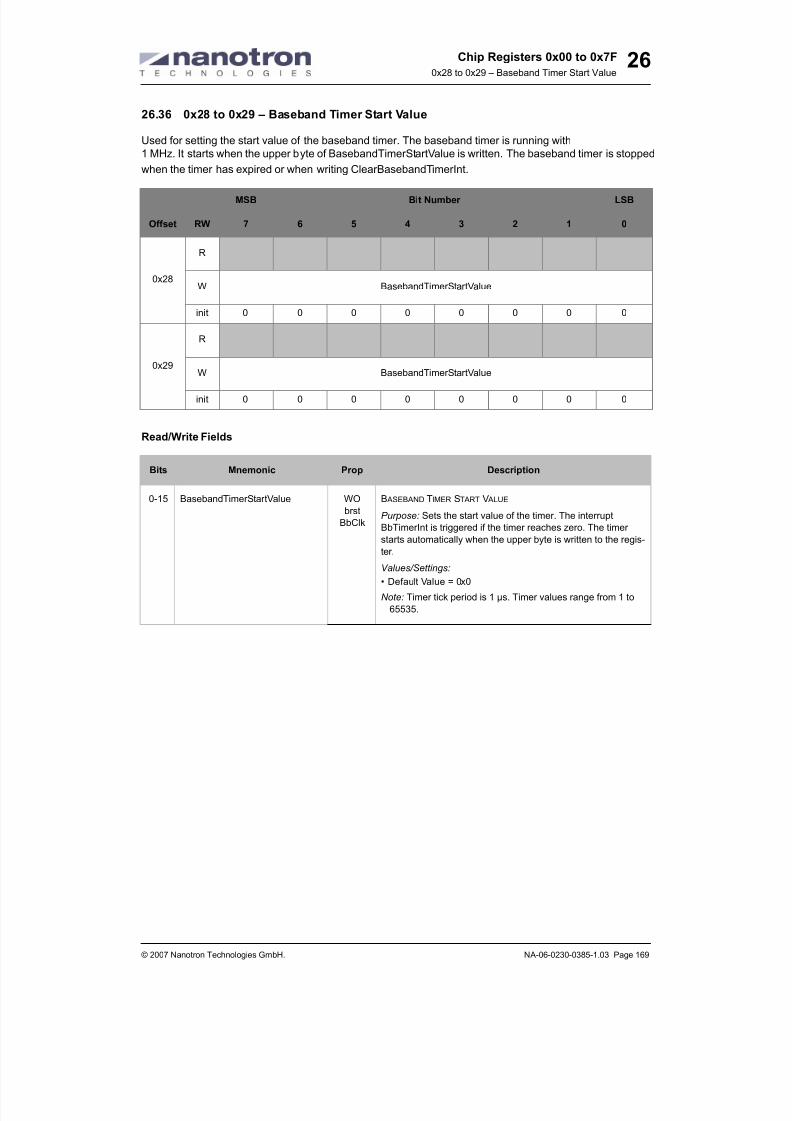
8/20/2019 nanoLOC NA5TR1 UserGuide
http://slidepdf.com/reader/full/nanoloc-na5tr1-userguide 185/325
Chip Registers 0x00 to 0x7F
0x28 to 0x29 – Baseband Timer Start Value
© 2007 Nanotron Technologies GmbH. NA-06-0230-0385-1.03 Page 169
26
26.36 0x28 to 0x29 – Baseband Timer Start Value
Used for setting the start value of the baseband timer. The baseband timer is running with
1 MHz. It starts when the upper byte of BasebandTimerStartValue is written. The baseband timer is stopped
when the timer has expired or when writing ClearBasebandTimerInt.
Read/Write Fields
MSB Bit Number LSB
Offset RW 7 6 5 4 3 2 1 0
0x28
R
W BasebandTimerStartValue
init 0 0 0 0 0 0 0 0
0x29
R
W BasebandTimerStartValue
init 0 0 0 0 0 0 0 0
Bits Mnemonic Prop Description
0-15 BasebandTimerStartValue WO
brst
BbClk
B ASEBAND TIMER START V ALUE
Purpose: Sets the start value of the timer. The interrupt
BbTimerInt is triggered if the timer reaches zero. The timer
starts automatically when the upper byte is written to the regis-
ter.
Values/Settings:
• Default Value = 0x0
Note: Timer tick period is 1 µs. Timer values range from 1 to
65535.

8/20/2019 nanoLOC NA5TR1 UserGuide
http://slidepdf.com/reader/full/nanoloc-na5tr1-userguide 186/325
Chip Registers 0x00 to 0x7F
0x2A to 0x2B – ToaOffset for Received Ack Packet
Page 170 NA-06-0230-0385-1.03 © 2007 Nanotron Technologies GmbH.
26
26.37 0x2A to 0x2B – ToaOffset for Received Ack Packet
Used for reporting the Time of Arrival Offset of a received Ack packet, and for reporting if the time measure-
ment is valid for the Ack packet.
Read Only Fields
MSB Bit Number LSB
Offset RW 7 6 5 4 3 2 1 0
0x2AR ToaOffsetMeanAck
init 0 0 0 0 0 0 0 0
0x2BR
Toa
Offset
Mean
AckValid
ToaOffsetMeanAck
init 0 0 0 0 0 0 0 0
Bits Mnemonic Prop Description
0-12 ToaOffsetMeanAck RO
BbClk
TO A OFFSET FOR RECEIVED ACK P ACKET
Purpose: Reports the Time of Arrival Offset of a received Ack
packet.
Values/Settings:
• Default Value = 0x0
15
(7)
ToaOffsetMeanAckValid RO
BbClk
V ALID ACK P ACKET
Purpose: Reports that enough pulses were received at end of
Ack packet.
Values/Settings:
Values/Settings:0

8/20/2019 nanoLOC NA5TR1 UserGuide
http://slidepdf.com/reader/full/nanoloc-na5tr1-userguide 187/325
Chip Registers 0x00 to 0x7F
0x2C to 0x2D – Round Trip Time
© 2007 Nanotron Technologies GmbH. NA-06-0230-0385-1.03 Page 171
26
26.38 0x2C to 0x2D – Round Trip Time
Used for reporting the round trip time of a transmitted Data packet and of a received Ack packet.
Read Only Fields
MSB Bit Number LSB
Offset RW 7 6 5 4 3 2 1 0
0x2CR TxRespTime
init 0 0 0 0 0 0 0 0
0x2DR TxRespTime
init 0 0 0 0 0 0 0 0
Bits Mnemonic Prop Description
0-15 TxRespTime RO
BbClk
TX RESPONSE ROUND TRIP TIME
Purpose: Reports the response time of the transmission of a
Data packet and the reception of the corresponding Acknowl-
edgement (one round trip).
Values/Settings:
• Default Value = 0x0
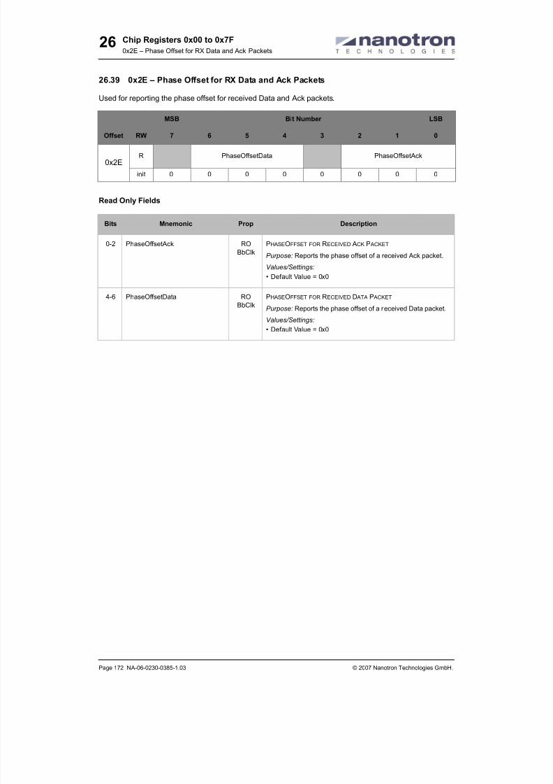
8/20/2019 nanoLOC NA5TR1 UserGuide
http://slidepdf.com/reader/full/nanoloc-na5tr1-userguide 188/325
Chip Registers 0x00 to 0x7F
0x2E – Phase Offset for RX Data and Ack Packets
Page 172 NA-06-0230-0385-1.03 © 2007 Nanotron Technologies GmbH.
26
26.39 0x2E – Phase Offset for RX Data and Ack Packets
Used for reporting the phase offset for received Data and Ack packets.
Read Only Fields
MSB Bit Number LSB
Offset RW 7 6 5 4 3 2 1 0
0x2ER PhaseOffsetData PhaseOffsetAck
init 0 0 0 0 0 0 0 0
Bits Mnemonic Prop Description
0-2 PhaseOffsetAck RO
BbClk
PHASEOFFSET FOR RECEIVED ACK P ACKET
Purpose: Reports the phase offset of a received Ack packet.
Values/Settings:
• Default Value = 0x0
4-6 PhaseOffsetData RO
BbClk
PHASEOFFSET FOR RECEIVED D ATA P ACKET
Purpose: Reports the phase offset of a received Data packet.
Values/Settings:
• Default Value = 0x0

8/20/2019 nanoLOC NA5TR1 UserGuide
http://slidepdf.com/reader/full/nanoloc-na5tr1-userguide 189/325
Chip Registers 0x00 to 0x7F
0x2F to 0x30 – ToaOffset for Received Data Packet
© 2007 Nanotron Technologies GmbH. NA-06-0230-0385-1.03 Page 173
26
26.40 0x2F to 0x30 – ToaOffset for Received Data Packet
Used for reporting the Time of Arrival of a received Data packet, and for reporting if enough pulses were
received to provide a valid time measurement.
Read Only Fields
MSB Bit Number LSB
Offset RW 7 6 5 4 3 2 1 0
0x2FR ToaOffsetMeanData
init 0 0 0 0 0 0 0 0
0x30R
Toa
Offset
Mean
Data
Valid
ToaOffsetMeanData
init 0 0 0 0 0 0 0 0
Bits Mnemonic Prop Description
0-12 ToaOffsetMeanData RO
BbClk
TO A OFFSET FOR RECEIVED D ATA P ACKET
Purpose: Reports the time of arrival of a received Data packet.
Values/Settings:
• Default Value = 0x0
15
(7)
ToaOffsetMeanDataValid RO
BbClk
V ALID D ATA P ACKET
Purpose: Reports if enough pulses were received to provide a
valid time measurement.
Values/Settings:
• Default Value = 0x0

8/20/2019 nanoLOC NA5TR1 UserGuide
http://slidepdf.com/reader/full/nanoloc-na5tr1-userguide 190/325
Chip Registers 0x00 to 0x7F
0x2A to 0x31 – Transceiver SyncWord (Write Only)
Page 174 NA-06-0230-0385-1.03 © 2007 Nanotron Technologies GmbH.
26
26.41 0x2A to 0x31 – Transceiver SyncWord (Write Only)
Used for defining the SyncWord, which is used for frame synchronization during reception (correlation).
Write Only Fields
MSB Bit Number LSB
Offset RW 7 6 5 4 3 2 1 0
0x2AW SyncWord
init 1 0 1 0 1 0 1 1
0x2BW SyncWord
init 0 0 1 0 1 1 0 0
0x2CW SyncWord
init 1 1 0 1 0 1 0 1
0x2DW SyncWord
init 1 0 0 1 0 0 1 0
0x2EW SyncWord
init 1 0 0 1 0 1 0 0
0x2FW SyncWord
init 1 1 0 0 1 0 1 0
0x30W SyncWord
init 0 1 1 0 1 0 0 1
0x31W SyncWord
init 1 0 1 0 1 0 1 1
Bits Mnemonic Prop Description
0-63 SyncWord WO
brst
BbClk
SET TRANSCEIVER SYNCWORD
Purpose: Defines the synchronization word which is used for
frame synchronization.
Values/Settings:
• Default Value = 0x0xAB69CA9492D52CAB
Usage: Auto and transparent mode.
This register must be defined before:
TxCmdStart = True or RxCmdStart = True
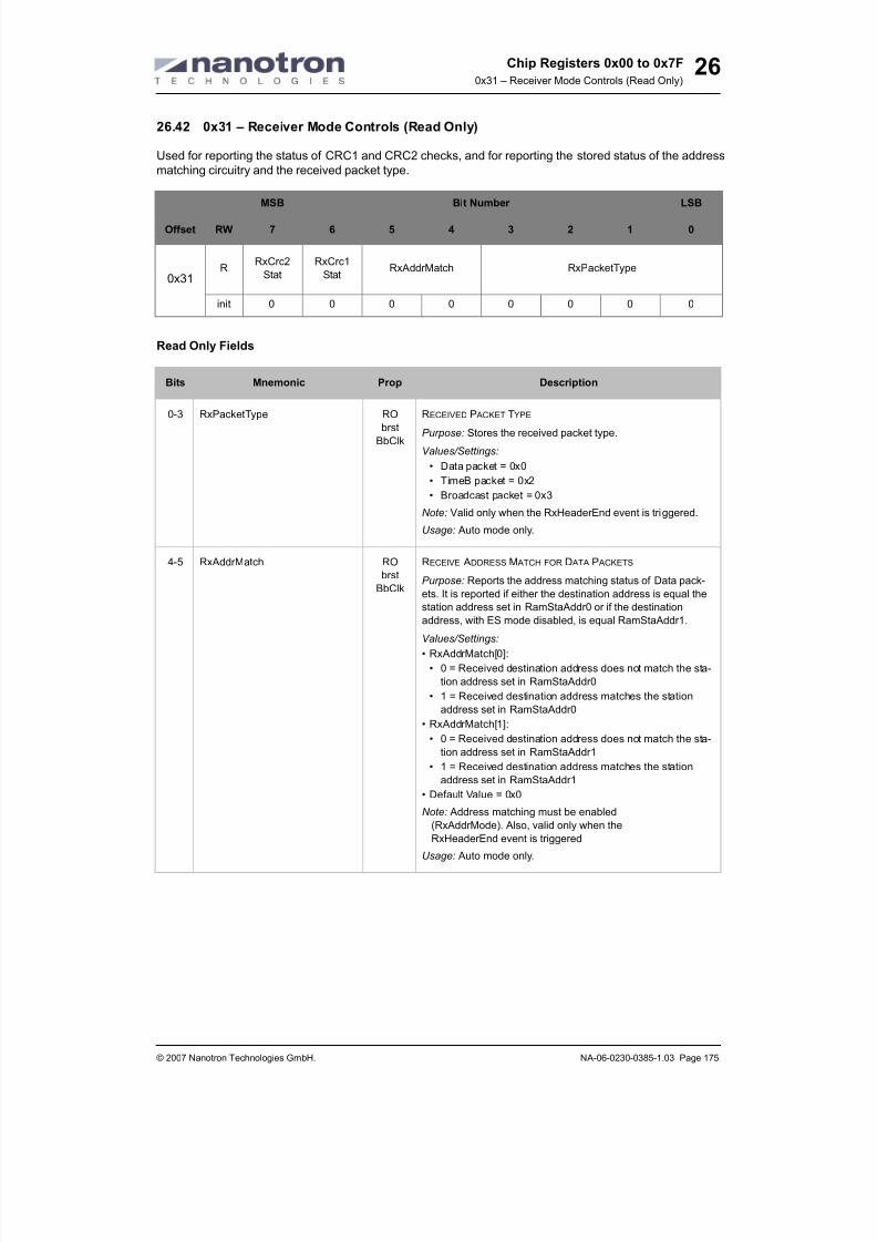
8/20/2019 nanoLOC NA5TR1 UserGuide
http://slidepdf.com/reader/full/nanoloc-na5tr1-userguide 191/325
Chip Registers 0x00 to 0x7F
0x31 – Receiver Mode Controls (Read Only)
© 2007 Nanotron Technologies GmbH. NA-06-0230-0385-1.03 Page 175
26
26.42 0x31 – Receiver Mode Controls (Read Only)
Used for reporting the status of CRC1 and CRC2 checks, and for reporting the stored status of the address
matching circuitry and the received packet type.
Read Only Fields
MSB Bit Number LSB
Offset RW 7 6 5 4 3 2 1 0
0x31R
RxCrc2
Stat
RxCrc1
StatRxAddrMatch RxPacketType
init 0 0 0 0 0 0 0 0
Bits Mnemonic Prop Description
0-3 RxPacketType RO
brst
BbClk
RECEIVED P ACKET TYPE
Purpose: Stores the received packet type.
Values/Settings:
• Data packet = 0x0
• TimeB packet = 0x2
• Broadcast packet = 0x3
Note: Valid only when the RxHeaderEnd event is triggered.
Usage: Auto mode only.
4-5 RxAddrMatch RO
brst
BbClk
RECEIVE ADDRESS M ATCH FOR D ATA P ACKETS
Purpose: Reports the address matching status of Data pack-
ets. It is reported if either the destination address is equal thestation address set in RamStaAddr0 or if the destination
address, with ES mode disabled, is equal RamStaAddr1.
Values/Settings:
• RxAddrMatch[0]:
• 0 = Received destination address does not match the sta-
tion address set in RamStaAddr0
• 1 = Received destination address matches the station
address set in RamStaAddr0
• RxAddrMatch[1]:
• 0 = Received destination address does not match the sta-
tion address set in RamStaAddr1
• 1 = Received destination address matches the station
address set in RamStaAddr1
• Default Value = 0x0
Note: Address matching must be enabled
(RxAddrMode). Also, valid only when the
RxHeaderEnd event is triggered
Usage: Auto mode only.

8/20/2019 nanoLOC NA5TR1 UserGuide
http://slidepdf.com/reader/full/nanoloc-na5tr1-userguide 192/325
Chip Registers 0x00 to 0x7F
0x31 – Receiver Mode Controls (Read Only)
Page 176 NA-06-0230-0385-1.03 © 2007 Nanotron Technologies GmbH.
26
6 RxCrc1Stat RO
brst
BbClk
STATUS OF CRC1 CHECK (FOR MAC HEADER)
Purpose: Reports the status of the CRC1 check.
Values/Settings:
• 0 = CRC1 check has failed
• 1 = CRC1 check was successful
• Default Value = 0x0
Note: Valid only when the RxHeaderEnd event is triggered.
This register just makes sense for TimeB packets when
RxTimeBCrc1Mode == NA_RxTimeBCrc1ModeOn_BC_C.
Usage: Auto mode only.
7 RxCrc2Stat RO
brst
BbClk
STATUS OF CRC2 CHECK (FOR P AYLOAD)
Purpose: Reports the status of the CRC2 check.
Values/Settings:
• 0 = CRC2 check has failed• 1 = CRC2 check was successful
• Default Value = 0x0
Note: Valid only when the RxEnd event is triggered.
Usage: Auto mode only.
Bits Mnemonic Prop Description

8/20/2019 nanoLOC NA5TR1 UserGuide
http://slidepdf.com/reader/full/nanoloc-na5tr1-userguide 193/325
Chip Registers 0x00 to 0x7F
0x32 – Receive Correlator Error Controls
© 2007 Nanotron Technologies GmbH. NA-06-0230-0385-1.03 Page 177
26
26.43 0x32 – Receive Correlator Error Controls
Used for defining the maximum allowed bit errors when a received pattern is correlated to the
SyncWord. It is also used for reading the number of bit errors occurred during SyncWord correlation.
Read Only Fields
Write Only Fields
MSB Bit Number LSB
Offset RW 7 6 5 4 3 2 1 0
0x32
R RxCorrBitErr
init 0 0 0 0 0 0 0 0
W RxCorrErrThres
init 0 0 1 1 0 0 0 0
Bits Mnemonic Prop Description
0-3 RxCorrBitErr RO
brst
BbClk
NUMBER OF SYNCWORD ERRORS
Purpose: Reports the number of bit errors that have occurred
during Syncword correlation.
Values/Settings:
• Default Value = 0x0
Note: Register is valid when the RxHeaderEnd event is trig-
gered.
Usage: Auto mode only.
Bits Mnemonic Prop Description
4-7 RxCorrErrThres WO
brst
BbClk
M AXIMUM ALLOWABLE SYNCWORD ERRORS
Purpose: It defines the threshold for bit errors allowed during
the correlation of a received pattern against the Syncword
stored in register 0x2A (SyncWord). If the occurred bit errors
are equal to or less than RxCorrErrThres, then the receiver
synchronizes.
Values/Settings:• Allowed values are between 0 and 15.
• Default Value = 0x3
This register must be defined before:
RxCmdStart = True
Usage: Auto and transparent mode.

8/20/2019 nanoLOC NA5TR1 UserGuide
http://slidepdf.com/reader/full/nanoloc-na5tr1-userguide 194/325
Chip Registers 0x00 to 0x7F
0x33 to 0x34 – Transmit Time Slot Start (Write Only)
Page 178 NA-06-0230-0385-1.03 © 2007 Nanotron Technologies GmbH.
26
26.44 0x33 to 0x34 – Transmit Time Slot Start (Write Only)
Used for defining the beginning of the time slot for a transmission.
Write Only Fields
MSB Bit Number LSB
Offset RW 7 6 5 4 3 2 1 0
0x33W TxTimeSlotStart
init 0 0 0 0 0 0 0 0
0x34W TxTimeSlotStart
init 0 0 0 0 0 0 0 0
Bits Mnemonic Prop Description
0-15 TxTimeSlotStart WO
brst
BbClk
SET TRANSMIT TIME SLOT START
Purpose: Defines the beginning of the time slot for a transmis-
sion. Used with TxTimeSlotControl.
Values/Settings:
• Only the 16 LSBs of the RTC value are compared to
TxTimeSlotStart. If both values are equal, then the time slot
begins.
• Default Value = 0x0
This register must be defined before:
TxCmdStart = True.Usage: Auto mode only.

8/20/2019 nanoLOC NA5TR1 UserGuide
http://slidepdf.com/reader/full/nanoloc-na5tr1-userguide 195/325
Chip Registers 0x00 to 0x7F
0x35 to 0x36 – Transmit Time Slot End (Write Only)
© 2007 Nanotron Technologies GmbH. NA-06-0230-0385-1.03 Page 179
26
26.45 0x35 to 0x36 – Transmit Time Slot End (Write Only)
Used for defining the end of the time slot for a transmission.
Write Only Fields
MSB Bit Number LSB
Offset RW 7 6 5 4 3 2 1 0
0x35W TxTimeSlotEnd
init 0 0 0 0 0 0 0 0
0x36W TxTimeSlotEnd
init 0 0 0 0 0 0 0 0
Bits Mnemonic Prop Description
0-15 TxTimeSlotEnd WO
brst
BbClk
SET TRANSMIT TIME SLOT END
Purpose: Defines the end of the time slot for a transmission.
Used with TxTimeSlotControl.
Values/Settings:
• Only the 16 LSBs of the RTC value are compared to
TxTimeSlotEnd. If both values are equal, then the time slot
ends.
This register must be defined before:
TxCmdStart = True
Usage: Auto mode only.

8/20/2019 nanoLOC NA5TR1 UserGuide
http://slidepdf.com/reader/full/nanoloc-na5tr1-userguide 196/325
Chip Registers 0x00 to 0x7F
0x33 – Receiver Encryption (Read Only)
Page 180 NA-06-0230-0385-1.03 © 2007 Nanotron Technologies GmbH.
26
26.46 0x33 – Receiver Encryption (Read Only)
Used for reporting the status of End Station and Intermediate Station address matching, as well as for
reporting the value of the three encryption control fields: CryptEn, CryptID, and CryptSeqN.
Read Only Fields
MSB Bit Number LSB
Offset RW 7 6 5 4 3 2 1 0
0x33R
RxCrypt
SeqNRxCryptId
RxCrypt
En
RxAddr
Seg
IsMatch
RxAddr
Seg
EsMatch
init 0 0 0 0 0 0 0 0
Bits Mnemonic Prop Description
0 RxAddrSegEsMatch RO
brst
BbClk
RX ADDRESS SEGMENT END STATION (ES) M ATCH
Purpose: Shows the status of the segmented address match of
end station address part.
Values/Settings:
• 0 = End Station address does not match
• 1 = End Station address matches
• Default Value = 0x0
1 RxAddrSegIsMatch RO
brst
BbClk
RX ADDRESS SEGMENT INTERMEDIATE STATION (IS) M ATCH
Purpose: Shows the status of the segmented address match of
Intermediate Station address part.Values/Settings:
• 0 = Intermediate Station address does not match
• 1 = Intermediate Station address matches
• Default Value = 0x0
4 RxCryptEn RO
brst
BbClk
V ALUE OF CRYPTEN BIT
Purpose: Reads the value of the one bit Encryption Enable
field, which is in the four bit EncryptionControl field inside the
MAC header.
Values/Settings:
• 0 = Disabled
• 1 = Enabled
• Default Value = 0x0
Note: Valid when the RxHeaderEnd event is triggered.
5-6 RxCryptId RO
brst
BbClk
V ALUE OF CRYPTID BITS
Purpose: Reads the value of the two bit Encryption ID field for
encrypted Data, Brdcast, and TimeB packets, which is in the
four bit EncryptionControl field inside the MAC header.
Values/Settings:
• Default Value = 0x0
Note: Valid when the RxHeaderEnd event is triggered.

8/20/2019 nanoLOC NA5TR1 UserGuide
http://slidepdf.com/reader/full/nanoloc-na5tr1-userguide 197/325
Chip Registers 0x00 to 0x7F
0x33 – Receiver Encryption (Read Only)
© 2007 Nanotron Technologies GmbH. NA-06-0230-0385-1.03 Page 181
26
7 RxCryptSeqN RO
brst
BbClk
V ALUE OF CRYPTSEQN BIT
Purpose: Reads the value of the one bit sequential numbering
scheme for encryption.
The receiver compares the last received against the present
CryptSeqN bit and increments its crypt clock value by one, if
they are not identical.
Values/Settings:
• Default Value = 0x0
Note: Valid when the RxHeaderEnd event is triggered.
Bits Mnemonic Prop Description

8/20/2019 nanoLOC NA5TR1 UserGuide
http://slidepdf.com/reader/full/nanoloc-na5tr1-userguide 198/325
Chip Registers 0x00 to 0x7F
0x34 to 0x35 – Receive FEC Single Bit Error Count (Read Only)
Page 182 NA-06-0230-0385-1.03 © 2007 Nanotron Technologies GmbH.
26
26.47 0x34 to 0x35 – Receive FEC Single Bit Error Count (Read Only)
Used for reporting the number of single bit errors that have occurred in a received packet.
Read Only Fields
MSB Bit Number LSB
Offset RW 7 6 5 4 3 2 1 0
0x34R RxFec1BitErr
init 0 0 0 0 0 0 0 0
0x35R RxFec1BitErr
init 0 0 0 0 0 0 0 0
Bits Mnemonic Prop Description
0-14 RxFec1BitErr RO
brst
BbClk
NUMBER OF CORRECTED FEC ERRORS
Purpose: Reports the number of correctable single bit errors
that have occurred in a receive packet.
Values/Settings:
• Default Value = 0x0
Note: Register is valid when the event RxEnd is triggered and
when UseFec == UseFecOn.
Usage: Auto mode only.

8/20/2019 nanoLOC NA5TR1 UserGuide
http://slidepdf.com/reader/full/nanoloc-na5tr1-userguide 199/325
Chip Registers 0x00 to 0x7F
0x36 – Reserved (Read Only)
© 2007 Nanotron Technologies GmbH. NA-06-0230-0385-1.03 Page 183
26
26.48 0x36 – Reserved (Read Only)
The Read Only fields in register 0x36 are reserved.
MSB Bit Number LSB
Offset RW 7 6 5 4 3 2 1 0
0x36R
init 0 0 0 0 0 0 0 0

8/20/2019 nanoLOC NA5TR1 UserGuide
http://slidepdf.com/reader/full/nanoloc-na5tr1-userguide 200/325
Chip Registers 0x00 to 0x7F
0x37 – Transmitter and Receiver Time Slot Control (TDMA)
Page 184 NA-06-0230-0385-1.03 © 2007 Nanotron Technologies GmbH.
26
26.49 0x37 – Transmitter and Receiver Time Slot Control (TDMA)
Used for enabling TX time slot control (TDMA) and RX time slot control (TDMA).
Write Only Fields
MSB Bit Number LSB
Offset RW 7 6 5 4 3 2 1 0
0x37
R
init 0 0 0 0 0 0 0 0
W
RxTime
Slot
Control
TxTime
Slot
Control
init 0 0 0 0 0 0 0 0
Bits Mnemonic Prop Description
0 TxTimeSlotControl WO
brst
BbClk
ENABLE TX TIME SLOT CONTROL (TDMA)
Purpose: Enables the TX time slot control so that packets are
transmitted only during the defined TX time slot.
Values/Settings:
• 0 = Disabled
Packets are transmitted independent of the time slot.
• 1 = Enabled
Packets are transmitted only during the defined TX time slot.
• Default Value = 0x0
This register must be defined before:
TxCmdStart = True
Usage: Auto mode only.
1 RxTimeSlotControl WO
brst
BbClk
RECEIVE TIME SLOT CONTROL
Purpose: Enables the RX time slot control so that at the begin-
ning of the defined RX time slot, the receiver is automatically
activated.
Values/Settings:
• 0 = Disabled
Activates the receiver independent of the defined time slot
through the RxCmd command.
• 1 = Enabled
Automatically activates the receiver at the beginning of the
defined RX time slot.
• Default Value = 0x0
Note: When enabled, the receive can still be manually acti-
vated through the RxCmd command.
Usage: Auto mode only.

8/20/2019 nanoLOC NA5TR1 UserGuide
http://slidepdf.com/reader/full/nanoloc-na5tr1-userguide 201/325
Chip Registers 0x00 to 0x7F
0x38 to 0x39 – RX Packet Slot (Read Only)
© 2007 Nanotron Technologies GmbH. NA-06-0230-0385-1.03 Page 185
26
26.50 0x38 to 0x39 – RX Packet Slot (Read Only)
Used for reporting the start time slot for receiving a packet by reading the 16 LSBs of the RTC value on a
header end event.
Read Only Fields
MSB Bit Number LSB
Offset RW 7 6 5 4 3 2 1 0
0x38R RxPacketSlot
init 0 0 0 0 0 0 0 0
0x39R RxPacketSlot
init 0 0 0 0 0 0 0 0
Bits Mnemonic Prop Description
0-15 RxPacketSlot RO
brst
BbClk
TIME (RTC) AT END OF HEADER
Purpose: Reports time (16 LSBs of RTC) at the packet header
end event.
Values/Settings:
• Default Value = 0x0
Note: Register is valid when the RxHeaderEnd event is trig-
gered.
Usage: Auto mode only.
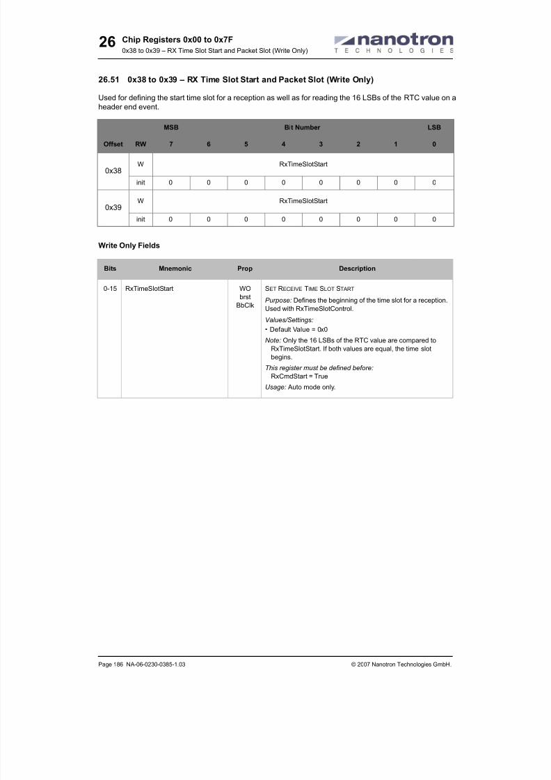
8/20/2019 nanoLOC NA5TR1 UserGuide
http://slidepdf.com/reader/full/nanoloc-na5tr1-userguide 202/325
Chip Registers 0x00 to 0x7F
0x38 to 0x39 – RX Time Slot Start and Packet Slot (Write Only)
Page 186 NA-06-0230-0385-1.03 © 2007 Nanotron Technologies GmbH.
26
26.51 0x38 to 0x39 – RX Time Slot Start and Packet Slot (Write Only)
Used for defining the start time slot for a reception as well as for reading the 16 LSBs of the RTC value on a
header end event.
Write Only Fields
MSB Bit Number LSB
Offset RW 7 6 5 4 3 2 1 0
0x38W RxTimeSlotStart
init 0 0 0 0 0 0 0 0
0x39W RxTimeSlotStart
init 0 0 0 0 0 0 0 0
Bits Mnemonic Prop Description
0-15 RxTimeSlotStart WO
brst
BbClk
SET RECEIVE TIME SLOT START
Purpose: Defines the beginning of the time slot for a reception.
Used with RxTimeSlotControl.
Values/Settings:
• Default Value = 0x0
Note: Only the 16 LSBs of the RTC value are compared to
RxTimeSlotStart. If both values are equal, the time slot
begins.
This register must be defined before:
RxCmdStart = True
Usage: Auto mode only.

8/20/2019 nanoLOC NA5TR1 UserGuide
http://slidepdf.com/reader/full/nanoloc-na5tr1-userguide 203/325
Chip Registers 0x00 to 0x7F
0x3A to 0x3B – RX Time Slot End
© 2007 Nanotron Technologies GmbH. NA-06-0230-0385-1.03 Page 187
26
26.52 0x3A to 0x3B – RX Time Slot End
Used for defining the end of the time slot for reception.
Write Only Fields
MSB Bit Number LSB
Offset RW 7 6 5 4 3 2 1 0
0x3A
R
init 0 0 0 0 0 0 0 0
W RxTimeSlotEnd
init 0 0 0 0 0 0 0 0
0x3B
R
init 0 0 0 0 0 0 0 0
W RxTimeSlotEnd
init 0 0 0 0 0 0 0 0
Bits Mnemonic Prop Description
0-15 RxTimeSlotEnd WO
brst
BbClk
SET RECEIVE TIME SLOT END
Purpose: Defines the end of the time slot for a reception. Used
with RxTimeSlotControl.
Values/Settings:
• Default Value = 0x0
Values/Settings:
Note: Only the 16 LSBs of the RTC value are compared to
RxTimeSlotEnd. If both values are equal, the time slot ends.
This register must be defined before:
RxCmdStart = True
Usage: Auto mode only.

8/20/2019 nanoLOC NA5TR1 UserGuide
http://slidepdf.com/reader/full/nanoloc-na5tr1-userguide 204/325
Chip Registers 0x00 to 0x7F
0x3C – ARQ
Page 188 NA-06-0230-0385-1.03 © 2007 Nanotron Technologies GmbH.
26
26.53 0x3C – ARQ
Used for setting the maximum value for packet retransmissions and for reporting the ARQ retransmission
counter value.
Read Only Fields
Write Only Fields
MSB Bit Number LSB
Offset RW 7 6 5 4 3 2 1 0
0x3C
R TxArqCnt
init 0 0 0 0 0 0 0 0
W TxArqMax
init 1 1 1 0 0 0 0 0
Bits Mnemonic Prop Description
0-3 TxArqCnt RO
brst
BbClk
TRANSMITTER ARQ COUNT (REQUIRED RETRANSMISSIONS)
Purpose: Reports the required number of retransmissions.
Values/Settings:
• Default Value = 0x0
Note: The following conditions are used to determine if the
transmission was successful or unsuccessful:
• If TxArqCnt <= TxArqMax, then the transmission was suc-
cessful.
• If TxArqCnt > TxArqMax, then the transmission was not
successful.
Bits Mnemonic Prop Description
4-7 TxArqMax WO
brst
BbClk
TRANSMIT ARQ M AXIMUM
Purpose: Sets the maximal value for packet retransmissions.
Values/Settings:
• The maximal allowed value is 14.
This register must be defined before:
TxCmdStart = True
Usage: Auto mode only.

8/20/2019 nanoLOC NA5TR1 UserGuide
http://slidepdf.com/reader/full/nanoloc-na5tr1-userguide 205/325
Chip Registers 0x00 to 0x7F
0x3D – RF Chirp Generator Controls
© 2007 Nanotron Technologies GmbH. NA-06-0230-0385-1.03 Page 189
26
26.54 0x3D – RF Chirp Generator Controls
Used for providing settings for the chirp generator and for accessing the Chirp Sequencer RAM.
Write Only Fields
MSB Bit Number LSB
Offset RW 7 6 5 4 3 2 1 0
0x3D
R
init 0 0 0 0 0 0 0 0
WInternal
Use Only
Csq
UseRam
Csq
Mem
AddrInit
Csq
Asy
Mode
Csq
Use
4Phases
CsqUse
Phase
Shift
CsqDitherValue
init 0 0 0 0 0 1 0 0
Bits Mnemonic Prop Description
0-1 CsqDitherValue WO
brst
BbClk
CHIRP SEQUENCER DITHER V ALUE
Purpose: Provides a dither function, which is used to delay
transmission based on settings made to this field. Each cycle is
equal to the frequency of LO div 20.
Values/Settings:
• 0 = No delay
• 1 = delay is 0 or 1 cycle (distribution 1:1)
• 2 = delay is 0, 1, or 2 cycles (distribution 1:1:1)
• 3 = delay is 0, 1, or 2 cycles (distribution 2:1:1)
• Default Value = 0x0
2 CsqUsePhaseShift WO
brst
BbClk
CHIRP SEQUENCER USE PHASE SHIFT
Purpose: Enables the pseudo-random feature of the chirp gen-
erator to improve the RF-spectrum of the transmitted chirps.
Causes transmission with 0° and 180° phase shift.
Values/Settings:
• 0 = Disable (phase shift is always 0°)
• 1 = Enable
• Default Value = 0x0
3 CsqUse4Phases WObrst
BbClk
USE FOUR PHASES
Purpose: Provides an additional 90° and 270° phase shift,
along with the 0° and 180° phases enabled by
CsqUsePhaseShift.
Values/Settings:
• 0 = Disable
• 1 = Enable
• Default Value = 0x0

8/20/2019 nanoLOC NA5TR1 UserGuide
http://slidepdf.com/reader/full/nanoloc-na5tr1-userguide 206/325
Chip Registers 0x00 to 0x7F
0x3D – RF Chirp Generator Controls
Page 190 NA-06-0230-0385-1.03 © 2007 Nanotron Technologies GmbH.
26
4 CsqAsyMode WO
brst
BbClk
SET ASYMMETRIC MODE
Purpose: When enabled, the Chirp Sequencer RAM is
addressed asymmetrically.
Values/Settings:
• 0 = Disable (access symmetrically: address increment AND
decrement)
• 1 = Enable (access increment only)
• Default Value = 0x0
5 CsqMemAddrInit WO
brst
strb
BbClk
INITIALIZE CHIRP SEQUENCER MEMORY ADDRESS
Purpose: Sets the address counter of the chirp generator
memory back to 0. Required before writing to a Chirp
Sequencer RAM column.
Values/Settings:
• 0 = Disable
• 1 = Enable
• Default Value = 0x0
6 CsqUseRam WO
brst
BbClk
USE CHIRP SEQUENCER RAM
Purpose: Enables the Chirp Sequencer RAM.
Values/Settings:
• 0 = Disable (default matrix is used)
• 1 = Enable
• Default Value = 0x0
Bits Mnemonic Prop Description

8/20/2019 nanoLOC NA5TR1 UserGuide
http://slidepdf.com/reader/full/nanoloc-na5tr1-userguide 207/325
Chip Registers 0x00 to 0x7F
0x3E – Internal Use Only (Write Only)
© 2007 Nanotron Technologies GmbH. NA-06-0230-0385-1.03 Page 191
26
26.55 0x3E – Internal Use Only (Write Only)
For Nanotron Internal use only. These bits must be set to 0.
MSB Bit Number LSB
Offset RW 7 6 5 4 3 2 1 0
0x3E
R
init 0 0 0 0 0 0 0 0
WInternal
Use Only
Internal
Use OnlyInternal Use Only
init 0 0 0 0 0 0 0 0
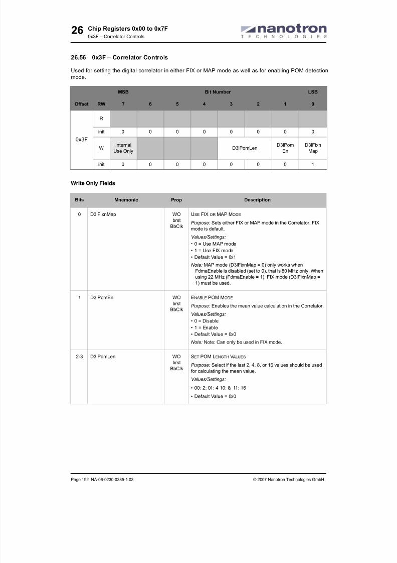
8/20/2019 nanoLOC NA5TR1 UserGuide
http://slidepdf.com/reader/full/nanoloc-na5tr1-userguide 208/325
Chip Registers 0x00 to 0x7F
0x3F – Correlator Controls
Page 192 NA-06-0230-0385-1.03 © 2007 Nanotron Technologies GmbH.
26
26.56 0x3F – Correlator Controls
Used for setting the digital correlator in either FIX or MAP mode as well as for enabling POM detection
mode.
Write Only Fields
MSB Bit Number LSB
Offset RW 7 6 5 4 3 2 1 0
0x3F
R
init 0 0 0 0 0 0 0 0
WInternal
Use OnlyD3lPomLen
D3lPom
En
D3lFixn
Map
init 0 0 0 0 0 0 0 1
Bits Mnemonic Prop Description
0 D3lFixnMap WO
brst
BbClk
USE FIX OR MAP MODE
Purpose: Sets either FIX or MAP mode in the Correlator. FIX
mode is default.
Values/Settings:
• 0 = Use MAP mode
• 1 = Use FIX mode
• Default Value = 0x1
Note: MAP mode (D3lFixnMap = 0) only works when
FdmaEnable is disabled (set to 0), that is 80 MHz only. When
using 22 MHz (FdmaEnable = 1), FIX mode (D3lFixnMap =
1) must be used.
1 D3lPomEn WO
brst
BbClk
ENABLE POM MODE
Purpose: Enables the mean value calculation in the Correlator.
Values/Settings:
• 0 = Disable
• 1 = Enable
• Default Value = 0x0
Note: Note: Can only be used in FIX mode.
2-3 D3lPomLen WObrst
BbClk
SET POM LENGTH V ALUES
Purpose: Select if the last 2, 4, 8, or 16 values should be used
for calculating the mean value.
Values/Settings:
• 00: 2; 01: 4 10: 8; 11: 16
• Default Value = 0x0

8/20/2019 nanoLOC NA5TR1 UserGuide
http://slidepdf.com/reader/full/nanoloc-na5tr1-userguide 209/325
Chip Registers 0x00 to 0x7F
0x40 – Frame Synchronization and Bit Synchronization
© 2007 Nanotron Technologies GmbH. NA-06-0230-0385-1.03 Page 193
26
26.57 0x40 – Frame Synchronization and Bit Synchronization
Switch back from MAP or FIX threshold1 to FIX threshold 0 detection in bitsync state when the in
LeaveMapThresh1InBitsync programmed number of bits has passed without the transceiver has reached
FrameSync state. The selection between MAP and FIX Threshold detection is programmed via Register
D3lFixnMap.
UseMapThresh1InFramesync is used to select the detection mode after the FrameSync state is reached.
Write Only Fields
MSB Bit Number LSB
Offset RW 7 6 5 4 3 2 1 0
0x40
R
init 0 0 0 0 0 0 0 0
W
UseMap
Thresh1InFrame
sync
LeaveMapThresh1InBitsync
init 0 0 0 0 0 0 1 1
Bits Mnemonic Prop Description
0-6 LeaveMapThresh1InBitsync WO
brst
BbClk
SWITCH B ACK TO FIX MODE WITH THRESHOLD 0
Purpose: Switch back to FIX mode using correlator
threshold 0 in bit synchronization state after programmednumber of detected pulses.
Values/Settings:
• Default Value = 0x3
7 UseMapThresh1InFramesync WO
brst
BbClk
USE MAP MODE OR FIX MODE WITH THRESHOLD 1 IN
FRAME SYNC STATE
Purpose: Switch to MAP mode or FIX mode using corre-
lator threshold 1 in frame synchronization state.
Values/Settings:
• 0 = FIX with Threshold0
• 1 = FIX with Threshold1 or MAP (D3LFixnMap)
• Default Value = 0x0

8/20/2019 nanoLOC NA5TR1 UserGuide
http://slidepdf.com/reader/full/nanoloc-na5tr1-userguide 210/325

8/20/2019 nanoLOC NA5TR1 UserGuide
http://slidepdf.com/reader/full/nanoloc-na5tr1-userguide 211/325
Chip Registers 0x00 to 0x7F
0x42 – Local Oscillator, Chirp Sequencer, and External PA Controls
© 2007 Nanotron Technologies GmbH. NA-06-0230-0385-1.03 Page 195
26
26.59 0x42 – Local Oscillator, Chirp Sequencer, and External PA Controls
Used for enabling the Local Oscillator, the LO divider, the chirp sequencer clock, and the external power
amplifier control pin.
Write Only Fields
MSB Bit Number LSB
Offset RW 7 6 5 4 3 2 1 0
0x42
R
init 0 0 0 0 0 0 0 0
WInternal
Use Only
Internal
Use Only
Internal
Use Only
Enable
ExtPA
Invert
RxClock
Enable
Csq
Clock
Enable
LOdiv10
Enable
LO
init 0 0 0 0 0 0 0 0
Bits Mnemonic Prop Description
0 EnableLO WO
brst
BbClk
ENABLE RF LOCAL OSCILLATOR
Purpose: Enables the Local Oscillator.
Values/Settings:
• 0 = Disable
• 1 = Enable
• Default Value = 0x0
Note: Required only for tuning the Local Oscillator and for pro-
gramming the Chirp Sequencer (CSQ) RAM.
1 EnableLOdiv10 WO
brst
BbClk
ENABLE LO FREQUENCY DIVIDE BY 10 FUNCTION
Purpose: When enabled, the LO frequency is divided by 10
and delivered to digital part.
Values/Settings:
• 0 = Disable
• 1 = Enable
• Default Value = 0x0
Note: Required only for tuning the Local Oscillator and for pro-
gramming the Chirp Sequencer (CSQ) RAM.
2 EnableCsqClock WObrst
BbClk
ENABLE CHIRP SEQUENCER CLOCK
Purpose: Enables the Chirp Sequencer (CSQ) clock.
Values/Settings:
• 0 = Disable
• 1 = Enable
• Default Value = 0x0
Note: Required only for programming the Chirp Sequencer
(CSQ) RAM.

8/20/2019 nanoLOC NA5TR1 UserGuide
http://slidepdf.com/reader/full/nanoloc-na5tr1-userguide 212/325
Chip Registers 0x00 to 0x7F
0x42 – Local Oscillator, Chirp Sequencer, and External PA Controls
Page 196 NA-06-0230-0385-1.03 © 2007 Nanotron Technologies GmbH.
26
3 InvertRxClock WO
brst
BbClk
CHANGING S AMPLING EDGE FOR RECEIVER
Note: It is recommended that this not be change. Use the
default value.
Values/Settings:
• 0 = Disable
• 1 = Enable
• Default Value = 0x0
4 EnableExtPA WO
brst
BbClk
ENABLE EXTERNAL POWER AMPLIFIER OUTPUT
Purpose: Enables the external power amplifier control pin to
allow the use of an external power amplifier. It must be set
when using an external power amplifier
Values/Settings:
• 0 = Deactivate pin
• 1 = Activate pin
Note: The pin is low-active during transmit cycles and has
high-impedance during non-transmit cycles.
Bits Mnemonic Prop Description

8/20/2019 nanoLOC NA5TR1 UserGuide
http://slidepdf.com/reader/full/nanoloc-na5tr1-userguide 213/325
Chip Registers 0x00 to 0x7F
0x43 – RF Rx Low Noise Amplifier and TX Power Amplifier Bias
© 2007 Nanotron Technologies GmbH. NA-06-0230-0385-1.03 Page 197
26
26.60 0x43 – RF Rx Low Noise Amplifier and TX Power Amplifier Bias
Used for adjusting the frequency of the LNA response, and for adjusting the power amplifier bias current.
Write Only Fields
MSB Bit Number LSB
Offset RW 7 6 5 4 3 2 1 0
0x43
R
init 0 0 0 0 0 0 0 0
W TxPaBias LnaFreqAdjust
init 0 0 0 0 0 0 1 1
Bits Mnemonic Prop Description
0-2 LnaFreqAdjust WO
brst
BbClk
ADJUST RF RECEIVER LNA FREQUENCY
Purpose: Frequency adjustment of the LNA (Low Noise Ampli-
fier) frequency response (S21).
Values/Settings:
• 111b – Shift the middle frequency of the LNA frequency
response to lower frequencies
• 000b – Shift the middle frequency of the LNA frequency
response to higher frequencies
• Default Value = 0x3 (recommended)
4-6 TxPaBias WO
brst
BbClk
ADJUST RF TRANSMITTER POWER AMPLIFIER BIAS
Purpose: Adjusts the PA bias current to compensate process
deviations.
Values/Settings:
• Default Value = 0x0 (recommended)

8/20/2019 nanoLOC NA5TR1 UserGuide
http://slidepdf.com/reader/full/nanoloc-na5tr1-userguide 214/325
Chip Registers 0x00 to 0x7F
0x44 – Transmitter Output Power (Data, TimeB, and BrdCast)
Page 198 NA-06-0230-0385-1.03 © 2007 Nanotron Technologies GmbH.
26
26.61 0x44 – Transmitter Output Power (Data, TimeB, and BrdCast)
Used for setting the RF transmitter output power for Data, TimeB (time beacon), and Brdcast (broadcast)
packets.
Write Only Fields
MSB Bit Number LSB
Offset RW 7 6 5 4 3 2 1 0
0x44
R
init 0 0 0 0 0 0 0 0
W TxOutputPower0
init 0 0 1 1 1 1 1 1
Bits Mnemonic Prop Description
0-5 TxOutputPower0 WO
brst
BbClk
ADJUST RF TX OUTPUT POWER 0
Purpose: Sets the transmitter output power for data (Data)
packets, time beacon (TimeB) packets, and broadcast (Brd-
Cast) packets.
Values/Settings:
• Default Value = 0x3F

8/20/2019 nanoLOC NA5TR1 UserGuide
http://slidepdf.com/reader/full/nanoloc-na5tr1-userguide 215/325
Chip Registers 0x00 to 0x7F
0x45 – Transmitter Output Power (Ack, Req2S, and Clr2S)
© 2007 Nanotron Technologies GmbH. NA-06-0230-0385-1.03 Page 199
26
26.62 0x45 – Transmitter Output Power (Ack, Req2S, and Clr2S)
Used for setting the RF Transmitter output power for Ack (acknowledgments), Req2S (request to send), and
Clr2S (clear to send) packets.
Write Only Fields
MSB Bit Number LSB
Offset RW 7 6 5 4 3 2 1 0
0x45
R
init 0 0 0 0 0 0 0 0
W TxOutputPower1
init 0 0 1 1 1 1 1 1
Bits Mnemonic Prop Description
0-5 TxOutputPower1 WO
brst
BbClk
ADJUST RF TX OUTPUT POWER 1
Purpose: Sets the transmitter output power for acknowledge-
ment packets (Ack), request to send (Req2S) packets, and
clear to send (Clr2S) packets.
Values/Settings:
• Default Value = 0x3F

8/20/2019 nanoLOC NA5TR1 UserGuide
http://slidepdf.com/reader/full/nanoloc-na5tr1-userguide 216/325
Chip Registers 0x00 to 0x7F
0x46 – Quantization Threshold for I
Page 200 NA-06-0230-0385-1.03 © 2007 Nanotron Technologies GmbH.
26
26.63 0x46 – Quantization Threshold for I
Used for programming the quantization threshold for the 5bit ADC for In-Phase value.
Write Only Fields
MSB Bit Number LSB
Offset RW 7 6 5 4 3 2 1 0
0x46
R
init 0 0 0 0 0 0 0 0
W RfRxCompValueI
init 0 0 0 0 1 1 1 1
Bits Mnemonic Prop Description
0-4 RfRxCompValueI WO
brst
BbClk
QUANTIZATION THRESHOLD FOR I
Values/Settings:
• Default Value = 0xF

8/20/2019 nanoLOC NA5TR1 UserGuide
http://slidepdf.com/reader/full/nanoloc-na5tr1-userguide 217/325
Chip Registers 0x00 to 0x7F
0x47 – Quantization Threshold for Q
© 2007 Nanotron Technologies GmbH. NA-06-0230-0385-1.03 Page 201
26
26.64 0x47 – Quantization Threshold for Q
Used for programming the quantization threshold for the 5bit ADC for Quadrature-Phase value.
Write Only Fields
MSB Bit Number LSB
Offset RW 7 6 5 4 3 2 1 0
0x47
R
init 0 0 0 0 0 0 0 0
W RfRxCompValueQ
init 0 0 0 0 1 1 1 1
Bits Mnemonic Prop Description
0 RfRxCompValueQ WO
brst
BbClk
QUANTIZATION THRESHOLD FOR Q
Values/Settings:
• Default Value = 0xF

8/20/2019 nanoLOC NA5TR1 UserGuide
http://slidepdf.com/reader/full/nanoloc-na5tr1-userguide 218/325
Chip Registers 0x00 to 0x7F
0x48 – Symbol Duration, Symbol Rate, and Modulation System
Page 202 NA-06-0230-0385-1.03 © 2007 Nanotron Technologies GmbH.
26
26.65 0x48 – Symbol Duration, Symbol Rate, and Modulation System
Used for determining the transmission behavior, including setting the symbol duration and the symbol rate,
as well as for setting a 2ary modulation system.
Write Only Fields
MSB Bit Number LSB
Offset RW 7 6 5 4 3 2 1 0
0x48
R
init 0 0 0 0 0 0 0 0
WInternal
Use OnlySymbolRate SymbolDur
init 0 1 1 0 0 0 1 1
Bits Mnemonic Prop Description
0-2 SymbolDur WO
BbClk
SET SYMBOL DURATION
Purpose: Set symbol duration between 500 ns and 4000 ns.
Values/Settings:
• NA_SymbolDur500ns_C (0x0)
• NA_SymbolDur1000ns_C (0x1)
• NA_SymbolDur2000ns_C (0x2)
• NA_SymbolDur4000ns_C (0x3)
• Default Value = 0x3
4-6 SymbolRate WO
BbClk
SET SYMBOL R ATE
Purpose: Sets the symbol rate between 12 k Symbols and 2M
Symbols
Values/Settings:
• NA_SymbolRate500kSymbols_VC_C (0x0)
• NA_SymbolRate1MSymbols_VC_C (0x1)
• NA_SymbolRate2MSymbols_VC_C (0x2)
• NA_SymbolRate125kSymbols_VC_C (0x6)
• NA_SymbolRate250kSymbols_VC_C (0x7)
• Default Value = 0x7

8/20/2019 nanoLOC NA5TR1 UserGuide
http://slidepdf.com/reader/full/nanoloc-na5tr1-userguide 219/325

8/20/2019 nanoLOC NA5TR1 UserGuide
http://slidepdf.com/reader/full/nanoloc-na5tr1-userguide 220/325
Chip Registers 0x00 to 0x7F
0x49 – CRC2, CRC2 Encryption, FEC, and Encryption Clock Mode
Page 204 NA-06-0230-0385-1.03 © 2007 Nanotron Technologies GmbH.
26
2 UseFec WO
brst
BbClk
ENABLE FORWARD ERROR CORRECTION (FEC)
Purpose: Purpose: Enables the forward error correction. Error
correction is applied to the complete MAC frame using a (7,4)block code.
Values/Settings:
• NA_UseFecOff_BC_C(0x0)
Disables FEC.
• NA_UseFecOn_BC_C(0x1)
Enables FEC.
• Default Value = 0x0
This register must be defined before: TxCmdStart = True or
RxCmdStart = True
Usage: Auto mode only.
3 TxRxCryptCrc2Mode WO
brst
BbClk
ENABLE ENCRYPTION/DECRYPTION CRC2 MODE
Purpose: Enables or disables the Encryption/Decryption of
CRC2.
Values/Settings:
• NA_TxRxCryptCrc2ModeUncrypted_BC_C(0x0)
In this mode, the CRC2 is calculated on the unencrypted
data, then appended and both the CRC2 and Data field are
encrypted.
The advantage of this method is that integrity checking is
possible. The disadvantage is that reception of the packet is
not possible without the key. No key means no reception (no
forwarding).
• NA_TxRxCryptCrc2ModeEncrypted_BC_C(0x1)
In this mode, the CRC2 is calculated on the encrypted data,
then the CRC2 is appended unencrypted to the encryptedData field.
The advantages of this method is that no key for data error
checking is needed and Forwarding is possible. The disad-
vantage is that no integrity checking is possible.
• Default Value = 0x0
This register must be defined before:
TxCmdStart = True or RxCmdStart = True
Usage: Auto mode only.
4-7 TxRxCryptClkMode WO
brst
BbClk
SET ENCRYPTION/DECRYPTION CLOCK MODE
Purpose: Selects the mode of the clock input value of the
stream cipher for each CryptId. Bit4 belongs to CryptId0, .. Bit
7 belongs to CryptId3.
Values/Settings:
• NA_TxRxCryptClkModeCryptClock_BC_C(0x0)
Uses the RamTxCryptClock / RamRxCryptClock values for
the clock input value calculating the en-/decryption key.
• NA_TxRxCryptClkModeScrambInit_BC_C(0x1)
The lowest 7 bits of the crypt clock (TxCryptClock /RxCrypt-
Clock are replaced by the value of the ScrambInit field. The
MSBs are taken from RamTxCryptClock / RamRxCryptClock
registers.
Note: For TX, the CryptID is taken from the
TxCryptID field while for RX, the CryptID is taken from the
received packet.
This register must be defined before:
TxCmdStart = True or RxCmdStart = TrueUsage: Auto mode only.
Bits Mnemonic Prop Description

8/20/2019 nanoLOC NA5TR1 UserGuide
http://slidepdf.com/reader/full/nanoloc-na5tr1-userguide 221/325
Chip Registers 0x00 to 0x7F
0x4A – Baseband Buffer and MACFrame Configuration
© 2007 Nanotron Technologies GmbH. NA-06-0230-0385-1.03 Page 205
26
26.67 0x4A – Baseband Buffer and MACFrame Configuration
Used for setting the Baseband buffer mode (Duplex or Simplex) and the MACFrame mode (Auto or Trans-
parent). It is also used for enabling FDMA which uses 22 MHz bandwidth and for swapping RX and TX
baseband buffers.
Read/Write Fields
MSB Bit Number LSB
Offset RW 7 6 5 4 3 2 1 0
0x4A
R
SwapBb
Buffers
init 0 0 0 0 0 0 0
WTxRx
Mode
Fdma
Enable
TxRxBb
Buffer
Mode0
TxRxBb
Buffer
Mode1
init 0 0 0 1 0 0 0 0
Bits Mnemonic Prop Description
0 SwapBbBuffers RW
brst
BbClk
EXCHANGE RX AND TX B ASEBAND BUFFERS
Purpose: Exchanges the buffers between the baseband trans-
mitter and receiver. When enabled, if a station is set up as an
intermediate station (IS), the station does not have to move
data from the RX buffer to the TX buffer.
Values/Settings:
• 0 = DefaultData in buffers belong to their intended direction.
• 1 = Enable data swapping
Data for the transmit operation are taken from the receive
buffer, while data of the receive operation are stored in trans-
mit buffer.
• Default Value = 0x0
Note: This is useful only in duplex mode.
See also: TxRxBbBufferMode1

8/20/2019 nanoLOC NA5TR1 UserGuide
http://slidepdf.com/reader/full/nanoloc-na5tr1-userguide 222/325
Chip Registers 0x00 to 0x7F
0x4A – Baseband Buffer and MACFrame Configuration
Page 206 NA-06-0230-0385-1.03 © 2007 Nanotron Technologies GmbH.
26
Write Only Fields
Bits Mnemonic Prop Description
1 TxRxBbBufferMode1 WObrst
BbClk
B ASEBAND BUFFER MODE 1: DUPLEX OR SIMPLEX
Purpose: Sets the data buffer for TX and RX as either two blocks
(Duplex) or a single block (Simplex).
Values/Settings:
• NA_TxRxBufferMode1Duplex_BC_C (0x0)
Sets Duplex mode
In this mode, the data buffer is split into two blocks, one for TX
and one for RX. TX and RX buffer operations are independent
of each other.
• NA_TxRxBufferMode1Simplex_BC_C (0x1)
Sets Simplex mode.
In this mode, the complete buffer is used for TX and RX.
• Default Value = 0x0
Note: Buffer size and configuration depend on the combinationof TxRxBbBufferMode0 and TxRxBbBufferMode1.
2 TxRxBbBufferMode0 WO
brst
BbClk
B ASEBAND BUFFER MODE 0: AUTO OR TRANSPARENT
Purpose: Sets the TX and RX data as either two segments
(Auto) or all four segments (Transparent).
Values/Settings:
• NA_TxRxBufferMode0Auto_BC_C (0x0)
Sets Auto mode: TX/RX buffer size = 256 bytes.
In this mode, the upper half of the Baseband RAM (two seg-
ments totalling 256 bytes) is used for data, as either a TX or a
RX buffer. The other two segments totalling 256 bytes are
reserved for the following:
• MAC frame header data
• Station addresses
• Encryption keys and related control values
• RTC snapshots
• NA_TxRxBufferMode0Transparent_BC_C (0x1)
In this mode, the complete Baseband RAM (all four segments
totalling 512 bytes) is used for data, as either a TX or a RX
buffer.
• Default Value = 0x0
Note: Buffer size and configuration depend on the combination
of TxRxBbBufferMode0 and TxRxBbBufferMode1.
4 FdmaEnable WO
brst
BbClk
ENABLES FDMA
Purpose: Enables FDMA (Frequency Division Multiple Access),
which uses 22 MHz bandwidth. When disabled, 80 MHz band-
width is used.
Values/Settings:
• 0 = Disable
• 1 = Enable
• Default Value = 0x1

8/20/2019 nanoLOC NA5TR1 UserGuide
http://slidepdf.com/reader/full/nanoloc-na5tr1-userguide 223/325
Chip Registers 0x00 to 0x7F
0x4A – Baseband Buffer and MACFrame Configuration
© 2007 Nanotron Technologies GmbH. NA-06-0230-0385-1.03 Page 207
26
7 TxRxMode WO
brst
BbClk
MACFRAME MODE: AUTO AND TRANSPARENT
Purpose: When using auto mode, the MACFrame is built as a
nanoLOC MACFrame that includes MAC header information aswell as payload data. When using transparent mode, the com-
plete MACFrame is considered data.
Values/Settings:
• NA_TxRxModeAuto_BC_C (0x0)
Sets Auto mode.
In this mode, each MACFrame is built with a MAC header and
payload data. For TX, software need only deliver the bytes for
the data part, while for RX only the data part is returned to soft-
ware.
• NA_TxRxModeTransparent_BC_C (0x1)
Sets Transparent mode.
In this mode, the complete MACFrame is interpreted as data.
For TX, software delivers all bytes of the MACFrame, while for
RX all bytes are returned to software.
• Default Value = 0x0
Bits Mnemonic Prop Description

8/20/2019 nanoLOC NA5TR1 UserGuide
http://slidepdf.com/reader/full/nanoloc-na5tr1-userguide 224/325
Chip Registers 0x00 to 0x7F
0x4B to 0x4C – Transceiver Chirp Matrix
Page 208 NA-06-0230-0385-1.03 © 2007 Nanotron Technologies GmbH.
26
26.68 0x4B to 0x4C – Transceiver Chirp Matrix
In a 2ary system, each bit (whose possible values are either 0 or 1) is represented as a chirp pulse.
ChirpMatrix0 selects the type of chirp pulse which represents the value 0. ChirpMatrix1 selects the type of
chirp pulse that represents the value 1.
The pulse types include Upchirp, Downchirp, Folded Minus Pulse, Plus Folded Pulse, and Off Chirp. See
also Pulse Types on page 208.
Pulse Types
For each of ChirpMatrix0, ChirpMatrix1, ChirpMatrix2, and ChirpMatrix3, select one of the pulse types aslisted in the following table.
MSB Bit Number LSB
Offset RW 7 6 5 4 3 2 1 0
0x4B
R
init 0 0 0 0 0 0 0 0
W ChirpMatrix1 ChirpMatrix0
init 0 0 0 1 0 0 0 0
0x4C
R
init 0 0 0 0 0 0 0 0
W ChirpMatrix3 ChirpMatrix2
init 0 1 0 0 0 0 1 1
To Set Pulse Type Use This Constant Hex Value
Downchirp NA_ChirpDown_VC_C 0x0
Upchirp NA_ChirpUp_VC_C 0x1
Minus Folded Chirp NA_ChirpFoldMinus_VC_C 0x2
Plus Folded Chirp NA_ChirpFoldPlus_VC_C 0x3
Off Chirp NA_ChirpOff_VC_C 0x4

8/20/2019 nanoLOC NA5TR1 UserGuide
http://slidepdf.com/reader/full/nanoloc-na5tr1-userguide 225/325
Chip Registers 0x00 to 0x7F
0x4B to 0x4C – Transceiver Chirp Matrix
© 2007 Nanotron Technologies GmbH. NA-06-0230-0385-1.03 Page 209
26
Setting Pulse Types for a 2Ary System
Bits Mnemonic Prop Description
0-2 ChirpMatrix0 WObrst
BbClk
SET PULSE TYPE FOR V ALUES 0Values/Settings:
• Select pulse type (see table above)
• Default Value = 0x0
This register must be defined before:
TxCmdStart = True or RxCmdStart = True
4-6 ChirpMatrix1 WO
brst
BbClk
SET PULSE TYPE FOR V ALUE 1
Values/Settings:
• Select pulse type (see table above)
• Default Value = 0x1
This register must be defined before:
TxCmdStart = True or RxCmdStart = True

8/20/2019 nanoLOC NA5TR1 UserGuide
http://slidepdf.com/reader/full/nanoloc-na5tr1-userguide 226/325
Chip Registers 0x00 to 0x7F
0x4D – TX Underrun, CIFS Waiting, and Preamble/Tail Sequences
Page 210 NA-06-0230-0385-1.03 © 2007 Nanotron Technologies GmbH.
26
26.69 0x4D – TX Underrun, CIFS Waiting, and Preamble/Tail Sequences
Used for setting the value of symbol 0 or 1 in the MACFrame Preamble and Tail. It is also used for enabling
the aborting of a transmission through the use of the TxCmdStop command, as well as for Disabling waiting
for CIFS (Common InterFrame Switching time). I
Note: Chirp pulses are transmitted in the following sequence:
+ TxPreTrailMatrix0
+ TxPreTrailMatrix1
+ TxPreTrailMatrix0
+ TxPreTrailMatrix1
+ and so on.
Note: An Off symbol cannot be used in the Preamble or the Tail. Therefore, in an Up/Off or Down/Off mod-
ulation system, both values must be the same value.
Write Fields
MSB Bit Number LSB
Offset RW 7 6 5 4 3 2 1 0
0x4D
R
init 0 0 0 0 0 0 0 0
WTxMac
CifsDis
TxUnder
run
Ignore
TxPreTrai lMatr ix1 TxPreTrailMatrix0
init 0 0 0 1 0 1 0 0
Bits Mnemonic Prop Description
0-1 TxPreTrailMatrix0 WO
brst
BbClk
V ALUE FOR SYMBOL 0 IN PREAMBLE AND T AIL (TRAIL)
Purpose: Sets the value of symbol 0 in the
MACFrame Preamble and Tail.
Values/Settings:
• Symbol used in TxRxChirpMatrix0 (0x0)
• Symbol used in TxRxChirpMatrix1 (0x1)
• Symbol used in TxRxChirpMatrix3 (0x2)
• Symbol used in TxRxChirpMatrix3 (0x3)
• Default Value = 0x0
This register must be defined before:
TxCmdStart = True or RxCmdStart = True
Usage: Auto and transparent mode.

8/20/2019 nanoLOC NA5TR1 UserGuide
http://slidepdf.com/reader/full/nanoloc-na5tr1-userguide 227/325

8/20/2019 nanoLOC NA5TR1 UserGuide
http://slidepdf.com/reader/full/nanoloc-na5tr1-userguide 228/325
Chip Registers 0x00 to 0x7F
0x4E – Media Access Control for Transmitter
Page 212 NA-06-0230-0385-1.03 © 2007 Nanotron Technologies GmbH.
26
26.70 0x4E – Media Access Control for Transmitter
Used for enabling virtual carrier sensing (with or without Ack packets), as well for enabling physical carrier
sensing using either RSSI or chirp detection. It is also used for enabling ARQ, which uses acknowledge-
ments, a three-way handshake mechanism (to avoid collisions and eliminate “hidden node” problems), and
a back-off mechanism for fair medium access.
Write Only Fields
MSB Bit Number LSB
Offset RW 7 6 5 4 3 2 1 0
0x4E
R
init 0 0 0 0 0 0 0 0
WTxFrag
Prio
TxBack
OffAlgTx3Way TxArq
TxVCarr
SensAck
TxPhCarr
SenseMode
TxVCarr
Sens
init 0 0 0 1 0 0 0 0
Bits Mnemonic Prop Description
0 TxVCarrSens WO
brst
BbClk
VIRTUAL C ARRIER SENSING
Purpose: Virtual Carrier Sensing calculates the end of the cur-
rent transmission based on information taken from the received
header.
When this carrier sense method is enabled, the NAV (Network
Allocation Vector) is calculated using the packet type and
Length field of received packets. Also, the transmitter suspends
medium access until the NAV expires.Values/Settings:
• NA_TxVCarrSensOff_BC_C (0x0)
• NA_TxVCarrSensOn_BC_C (0x1)
• Default Value = 0x0
This register must be defined before:
TxCmdStart = True
Usage: Auto mode only.

8/20/2019 nanoLOC NA5TR1 UserGuide
http://slidepdf.com/reader/full/nanoloc-na5tr1-userguide 229/325
Chip Registers 0x00 to 0x7F
0x4E – Media Access Control for Transmitter
© 2007 Nanotron Technologies GmbH. NA-06-0230-0385-1.03 Page 213
26
1-2 TxPhCarrSenseMode WO
brst
BbClk
PHYSICAL C ARRIER SENSING MODE: RSSI OR
CHIRP DETECTION
Purpose: Physical carrier sensing uses either RSSI or chirpsymbol detection. Using RSSI, if AgcGain is lower than
AgcRssiThreshold, then the carrier is busy. Using the other
method, if a chirp is detected, then the carrier is busy.
Physical carrier sensing mode can be based either on chirp
detection, RSSI threshold, or both chirp detection and RSSI
threshold.
Values/Settings:
• NA_TxPhCarrSensModeOff_VC_C (0x0)
Physical carrier sensing is not applied.
• NA_TxPhCarrSensModeSymbols_VC_C (0x1)
Physical carrier sensing is based on chirp symbol detection.
• NA_TxPhCarrSensModeRssi_VC_C (0x2)
Physical carrier sensing is based on an RSSI threshold.
• NA_TxPhCarrSensModeSymbolsRssi_VC_C (0x3)
Physical carrier sensing is based on both symbol detection
and RSSI threshold.
This register must be defined before:
TxCmdStart = True.
Usage: Auto and transparent mode.
3 TxVCarrSensAck WO
brst
BbClk
INCLUDE ACK P ACKETS FOR VIRTUAL C ARRIER SENSE
Purpose: Purpose: When virtual carrier Sense is enabled and
this bit is set the time of an Ack packet is taken into calculation
when calculating the NAV (Network Allocation Vector).
Values/Settings:
• NA_TxVCarrSensAckOff_BC_C (0x0)NAV calculation does not regard Ack packets.
• NA_TxVCarrSensAckOn_BC_C (0x1)
NAV calculation regards Ack packets.
This register must be defined before:
TxCmdStart = True.
Usage: Auto mode only.
4 TxArq WO
brst
BbClk
TX ARQ (AUTOMATIC REPEAT REQUEST) ERROR CORRECTION
SCHEME FOR D ATA P ACKETS
Purpose: When this bit is set, the station waits for an Ack packet
as a response to a transmitted Data packet.
Values/Settings:
• NA_TxArqOff_BC_C (0x0) ARQ is disabled.
When ARQ is disabled, the transmitter does not wait for an
Ack packet as a response to a Data packet.
• NA_TxArqOn_BC_C (0x1)
ARQ is enabled.
With ARQ, the transmitting station waits for an acknowledge-
ment (ACK packet). The packet is retransmitted automatically
if TxArqMax > 0.
Note: ARQ must be disabled for Brdcast and TimeB packets.
This register must be defined before:
TxCmdStart = True.
Usage: Auto mode only.
Bits Mnemonic Prop Description

8/20/2019 nanoLOC NA5TR1 UserGuide
http://slidepdf.com/reader/full/nanoloc-na5tr1-userguide 230/325
Chip Registers 0x00 to 0x7F
0x4E – Media Access Control for Transmitter
Page 214 NA-06-0230-0385-1.03 © 2007 Nanotron Technologies GmbH.
26
5 Tx3Way WO
brst
BbClk
THREE-W AY H ANDSHAKE
Purpose: The three-way handshake uses a Req2S and Clr2S
mechanism. It is only used with Data packets. It is not used withBrdcast and TimeB packets.
Values/Settings:
• NA_Tx3WayOff_BC_C (0x0)
Three-way handshake is disabled.
• NA_Tx3WayOn_BC_C (0x1)
Three-way handshake is enabled.
This register must be defined before:
TxCmdStart = True.
Usage: Auto mode only.
6 TxBackOffAlg WO
brst
BbClk
B ACK-OFF ALGORITHM
Purpose: The exponential back-off algorithm waits a specific
period of time before reattempting a transmission.
Values/Settings:
• NA_TxBackOffAlgOff_BC_C (0x0)
Back-off algorithm is disabled. The complete seed is taken
(see TxBackoffSeed) and the seed is not modified.
• NA_TxBackOffAlgOn_BC_C (0x1)
Back-off algorithm is enabled. The number of bits taken from
seeds are increased by one when a transmission is not
acknowledged.A random value of 3 bit size is taken for the first
transmission.
This register must be defined before:
TxCmdStart = True.
Usage: Auto mode only.
7 TxFragPrio WO
brst
BbClk
FRAGMENTATION PRIORITIZATION
Purpose: Enables fragmentation prioritization scheme used in
the back-off time algorithm.
Values/Settings:
• 0 = Disable
The MSB of the back-off counter is set with the MSB from the
random value.
• 1 = Enable
Sets the MSB of the Back-Off counter to value zero (higher
priority).
• Default Value = 0x0
This register must be defined before:
TxCmdStart = True.
Usage: Auto mode only.
Bits Mnemonic Prop Description

8/20/2019 nanoLOC NA5TR1 UserGuide
http://slidepdf.com/reader/full/nanoloc-na5tr1-userguide 231/325
Chip Registers 0x00 to 0x7F
0x4F – Back-Off Seed for Back-Off Time
© 2007 Nanotron Technologies GmbH. NA-06-0230-0385-1.03 Page 215
26
26.71 0x4F – Back-Off Seed for Back-Off Time
Used for setting the back-off seed, which is either the start value of the random number generator for expo-
nential back-off or the number of back-off slots which has to pass by before next media access will be
attempted.
Write Only Fields
MSB Bit Number LSB
Offset RW 7 6 5 4 3 2 1 0
0x4F
R
init 0 0 0 0 0 0 0 0
W TxBackOffSeed
init 0 0 0 0 0 0 0 0
Bits Mnemonic Prop Description
0-7 TxBackOffSeed WO
brst
BbClk
B ACK-OFF SEED
Purpose: Sets either the start value of the random number gen-
erator for exponential back-off or the number of the back-off
slots.
Values/Settings:
• If TxBackOffAlg = TxBackOffAlgOn, then this sets the seed
value for the pseudo-number generator. It can be set for every
packet and improves the random properties of exponential
Back-Off. .
• If TxBackOffAlg = TxBackOffAlgOff, then this sets the number
of Back-Off slots before the next media access will start.
Note: It is not mandatory to set this register.
Usage: Auto mode only.
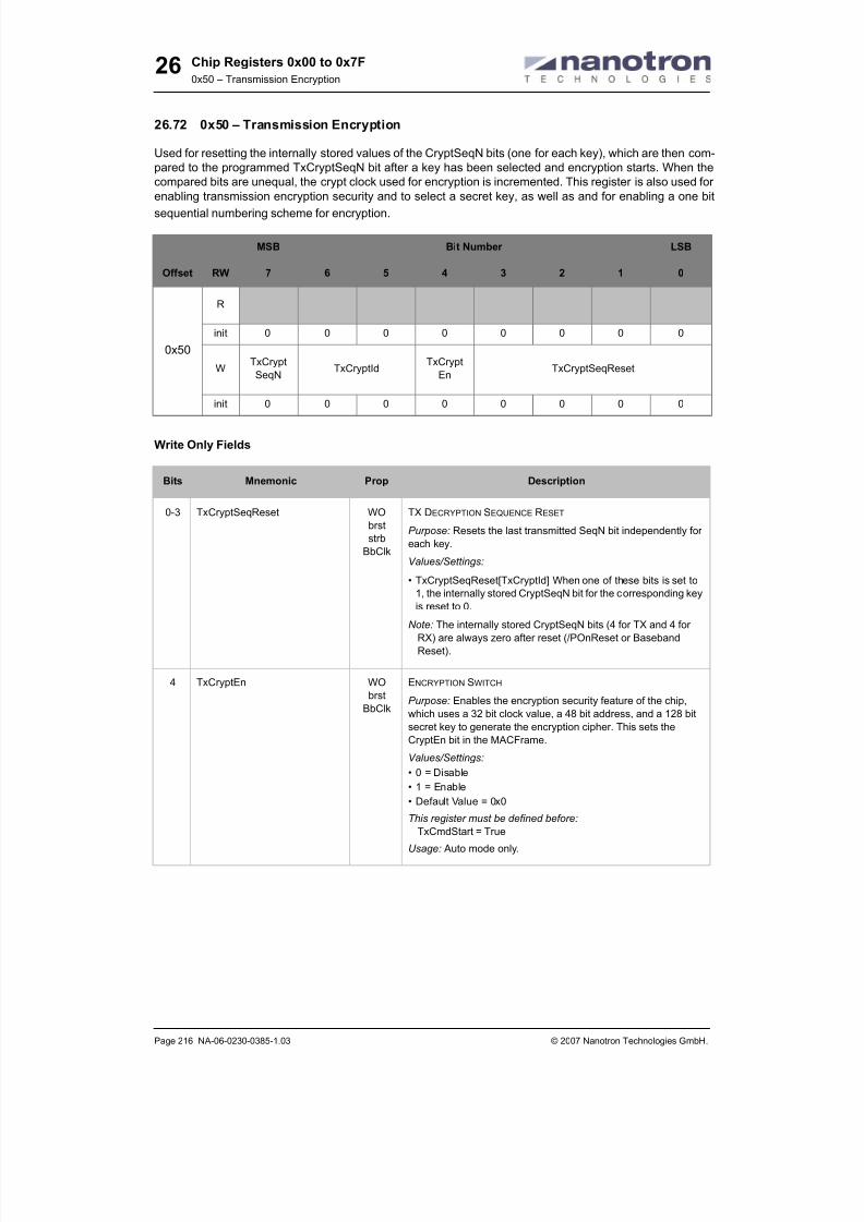
8/20/2019 nanoLOC NA5TR1 UserGuide
http://slidepdf.com/reader/full/nanoloc-na5tr1-userguide 232/325
Chip Registers 0x00 to 0x7F
0x50 – Transmission Encryption
Page 216 NA-06-0230-0385-1.03 © 2007 Nanotron Technologies GmbH.
26
26.72 0x50 – Transmission Encryption
Used for resetting the internally stored values of the CryptSeqN bits (one for each key), which are then com-
pared to the programmed TxCryptSeqN bit after a key has been selected and encryption starts. When the
compared bits are unequal, the crypt clock used for encryption is incremented. This register is also used for
enabling transmission encryption security and to select a secret key, as well as and for enabling a one bit
sequential numbering scheme for encryption.
Write Only Fields
MSB Bit Number LSB
Offset RW 7 6 5 4 3 2 1 0
0x50
R
init 0 0 0 0 0 0 0 0
WTxCrypt
SeqNTxCryptId
TxCrypt
EnTxCryptSeqReset
init 0 0 0 0 0 0 0 0
Bits Mnemonic Prop Description
0-3 TxCryptSeqReset WO
brst
strb
BbClk
TX DECRYPTION SEQUENCE RESET
Purpose: Resets the last transmitted SeqN bit independently for
each key.
Values/Settings:
• TxCryptSeqReset[TxCryptId] When one of these bits is set to1, the internally stored CryptSeqN bit for the corresponding key
is reset to 0.
Note: The internally stored CryptSeqN bits (4 for TX and 4 for
RX) are always zero after reset (/POnReset or Baseband
Reset).
4 TxCryptEn WO
brst
BbClk
ENCRYPTION SWITCH
Purpose: Enables the encryption security feature of the chip,
which uses a 32 bit clock value, a 48 bit address, and a 128 bit
secret key to generate the encryption cipher. This sets the
CryptEn bit in the MACFrame.
Values/Settings:
• 0 = Disable• 1 = Enable
• Default Value = 0x0
This register must be defined before:
TxCmdStart = True
Usage: Auto mode only.

8/20/2019 nanoLOC NA5TR1 UserGuide
http://slidepdf.com/reader/full/nanoloc-na5tr1-userguide 233/325
Chip Registers 0x00 to 0x7F
0x50 – Transmission Encryption
© 2007 Nanotron Technologies GmbH. NA-06-0230-0385-1.03 Page 217
26
5-6 TxCryptId WO
brst
BbClk
SECRET KEY SELECTION FOR ENCRYPTION
Purpose: Selects one of four secret keys as well as one of the
four TX crypt clocks, which are found in page 1 of the basebandRAM. It is only used for Data packets, Brdcast packets and
TimeB packets as only data is encrypted and other packet types
have no data fields.
Values/Settings:
• Select first secret key (0x0)
• Select second secret key (0x1)
• Select third secret key (0x2)
• Select fourth secret key (0x3)
See also: 0.
This register must be defined before:
TxCmdStart = True
Usage: Auto mode only.
7 TxCryptSeqN WO
brst
BbClk
ENCRYPTION SEQUENCE NUMBER
Purpose: This bit is compared to the internally stored CryptSeqN
bit (the TxCryptseqN bit of last transmission) of the correspond-
ing key. If they are unequal then the used crypt clock is incre-
mented before generating the cipher.
Values/Settings:
• Default Value = 0x0
This register must be defined before:
TxCmdStart = True
Usage: Auto mode only.
Bits Mnemonic Prop Description

8/20/2019 nanoLOC NA5TR1 UserGuide
http://slidepdf.com/reader/full/nanoloc-na5tr1-userguide 234/325
Chip Registers 0x00 to 0x7F
0x51 – Transmit Scrambler
Page 218 NA-06-0230-0385-1.03 © 2007 Nanotron Technologies GmbH.
26
26.73 0x51 – Transmit Scrambler
Used for enabling scrambling of TX packets and for initializing the bit scrambler.
Write Only Fields
MSB Bit Number LSB
Offset RW 7 6 5 4 3 2 1 0
0x51
R
init 0 0 0 0 0 0 0 0
W
Tx
Scramb
En
TxScrambInit
init 1 1 1 1 1 1 1 1
Bits Mnemonic Prop Description
0-6 TxScrambInit WO
brst
BbClk
TX SCRAMBLING INITIALIZATION
Purpose: Initializes the value for the scrambling unit.
Values/Settings:
• Default Value = 0x7F
Note: Do NOT program TxScrambInit with 0x00.
Note: There is no need to initialize the scrambler for each
packet.
This register must be defined before:TxCmdStart = True
Usage: Auto mode only.
7 TxScrambEn WO
brst
BbClk
TRANSMISSION SCRAMBLING
Purpose: Enables scrambling in a transmitted
MACFrame.
Values/Settings:
• 0 = Disable
Value 0 is intended for debugging purposes only.
• 1 = Enable
• Default Value = 0x1
Note: To randomize the data from highly redundant patterns,
scrambling must be enabled during normal operations.
This register must be defined before:
TxCmdStart = True
Usage: Auto mode only.

8/20/2019 nanoLOC NA5TR1 UserGuide
http://slidepdf.com/reader/full/nanoloc-na5tr1-userguide 235/325
Chip Registers 0x00 to 0x7F
0x52 to 0x53 – TX Data Size in Transparent Mode
© 2007 Nanotron Technologies GmbH. NA-06-0230-0385-1.03 Page 219
26
26.74 0x52 to 0x53 – TX Data Size in Transparent Mode
Used for setting the number of data bytes for transmission in Transparent mode.
Write Fields
MSB Bit Number LSB
Offset RW 7 6 5 4 3 2 1 0
0x52
R
init 0 0 0 0 0 0 0 0
W TxTransBytes
init 0 0 0 0 0 0 0 0
0x53
R
init 0 0 0 0 0 0 0 0
W TxTransBytes
init 0 0 0 0 0 0 0 0
Bits Mnemonic Prop Description
0-12 TxTransBytes WO
brst
BbClk
NUMBER OF D ATA BYTES IN TX MACFRAME IN TRANSPARENT
MODE
Purpose: When the transceiver is set in Transparent mode, thissets the number of bytes of data in the completed MACFrame
that is ready for transmission. These are all bytes between the
Syncword and the Tail.
Values/Settings:
• Default Value = 0x0
This register must be defined before:
TxCmdStart = True
Usage: Transparent mode only.
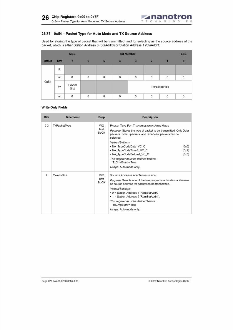
8/20/2019 nanoLOC NA5TR1 UserGuide
http://slidepdf.com/reader/full/nanoloc-na5tr1-userguide 236/325
Chip Registers 0x00 to 0x7F
0x54 – Packet Type for Auto Mode and TX Source Address
Page 220 NA-06-0230-0385-1.03 © 2007 Nanotron Technologies GmbH.
26
26.75 0x54 – Packet Type for Auto Mode and TX Source Address
Used for storing the type of packet that will be transmitted, and for selecting as the source address of the
packet, which is either Station Address 0 (StaAddr0) or Station Address 1 (StaAddr1).
Write Only Fields
MSB Bit Number LSB
Offset RW 7 6 5 4 3 2 1 0
0x54
R
init 0 0 0 0 0 0 0 0
WTxAddr
SlctTxPacketType
init 0 0 0 0 0 0 0 0
Bits Mnemonic Prop Description
0-3 TxPacketType WO
brst
BbClk
P ACKET TYPE FOR TRANSMISSION IN AUTO MODE
Purpose: Stores the type of packet to be transmitted. Only Data
packets, TimeB packets, and Broadcast packets can be
selected.
Values/Settings:
• NA_TypeCodeData_VC_C (0x0)
• NA_TypeCodeTimeB_VC_C (0x2)
• NA_TypeCodeBrdcast_VC_C (0x3)
This register must be defined before:
TxCmdStart = True
Usage: Auto mode only.
7 TxAddrSlct WO
brst
BbClk
SOURCE ADDRESS FOR TRANSMISSION
Purpose: Selects one of the two programmed station addresses
as source address for packets to be transmitted.
Values/Settings:
• 0 = Station Address 1 (RamStaAddr0)
• 1 = Station Address 2 (RamStaAddr1).
This register must be defined before:
TxCmdStart = True
Usage: Auto mode only.

8/20/2019 nanoLOC NA5TR1 UserGuide
http://slidepdf.com/reader/full/nanoloc-na5tr1-userguide 237/325
Chip Registers 0x00 to 0x7F
0x55 – Start/Stop Transmissions and TX Buffer Fill Command
© 2007 Nanotron Technologies GmbH. NA-06-0230-0385-1.03 Page 221
26
26.76 0x55 – Start/Stop Transmissions and TX Buffer Fill Command
Used for starting and stopping the transmitter and for setting a command that indicates that the lower sub-
block and/or upper subblock of the TX buffer is ready for transmission.
Write Only Fields
MSB Bit Number LSB
Offset RW 7 6 5 4 3 2 1 0
0x55
R
init 0 0 0 0 0 0 0 0
W TxBufferCmdTxCmd
Start
TxCmd
Stop
init 0 0 0 0 0 0 0 0
Bits Mnemonic Prop Description
0 TxCmdStop WO
brst
strb
BbClk
STOP TRANSMISSION
Purpose: This interrupts the current transmission by aborting the
transmission of a packet (in Auto mode) or stops/disables the
transmission (in Transparent mode). It also resets the transmit
buffer state.
Values/Settings:
• 0 = Default
• 1 = Stop transmission
• Default Value = 0x0
1 TxCmdStart WO
brst
strb
BbClk
START TRANSMISSION
Purpose: Starts the configured transmission. It initiates the
transmission of a packet (in Auto mode) or starts the transmis-
sion of data (in Transparent mode).
Values/Settings:
• 0 = Default
• 1 = Start transmission
• Default Value = 0x0
2-3 TxBufferCmd WO
brst
strbBbClk
Transmit Buffer Ready for Transmission
Purpose: Indicates that either the lower subblock and/or the
upper subblock of the TX Buffer is ready (filled) for transmission.
Values/Settings:
• Lower subblock filled for transmission LSB
• Upper subblock filled for transmission MSB
• Default Value = 0x0
Note: This command must be written after the TX buffer has
been written to with the data to be transmitted.
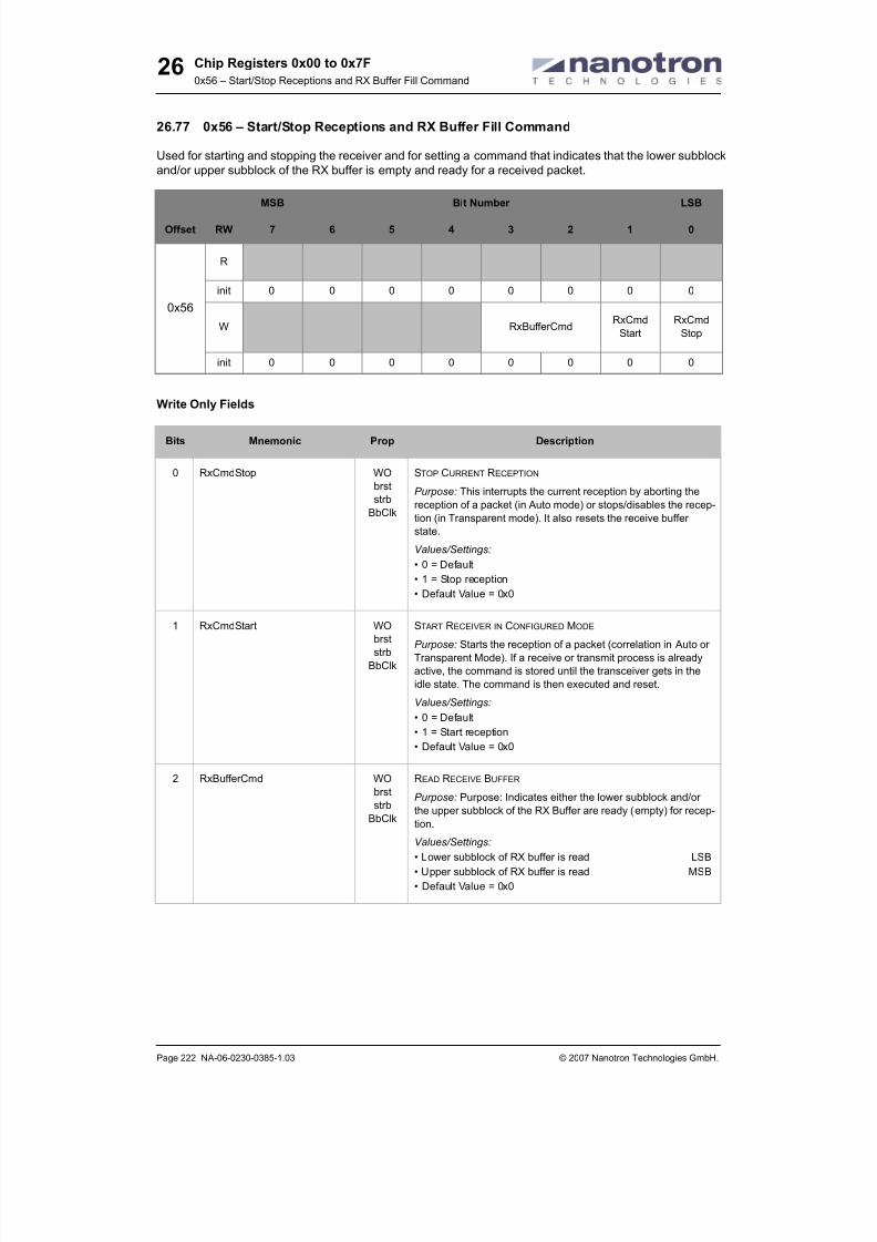
8/20/2019 nanoLOC NA5TR1 UserGuide
http://slidepdf.com/reader/full/nanoloc-na5tr1-userguide 238/325
Chip Registers 0x00 to 0x7F
0x56 – Start/Stop Receptions and RX Buffer Fill Command
Page 222 NA-06-0230-0385-1.03 © 2007 Nanotron Technologies GmbH.
26
26.77 0x56 – Start/Stop Receptions and RX Buffer Fill Command
Used for starting and stopping the receiver and for setting a command that indicates that the lower subblock
and/or upper subblock of the RX buffer is empty and ready for a received packet.
Write Only Fields
MSB Bit Number LSB
Offset RW 7 6 5 4 3 2 1 0
0x56
R
init 0 0 0 0 0 0 0 0
W RxBufferCmdRxCmd
Start
RxCmd
Stop
init 0 0 0 0 0 0 0 0
Bits Mnemonic Prop Description
0 RxCmdStop WO
brst
strb
BbClk
STOP CURRENT RECEPTION
Purpose: This interrupts the current reception by aborting the
reception of a packet (in Auto mode) or stops/disables the recep-
tion (in Transparent mode). It also resets the receive buffer
state.
Values/Settings:
• 0 = Default
• 1 = Stop reception
• Default Value = 0x0
1 RxCmdStart WO
brst
strb
BbClk
START RECEIVER IN CONFIGURED MODE
Purpose: Starts the reception of a packet (correlation in Auto or
Transparent Mode). If a receive or transmit process is already
active, the command is stored until the transceiver gets in the
idle state. The command is then executed and reset.
Values/Settings:
• 0 = Default
• 1 = Start reception
• Default Value = 0x0
2 RxBufferCmd WO
brststrb
BbClk
READ RECEIVE BUFFER
Purpose: Purpose: Indicates either the lower subblock and/or
the upper subblock of the RX Buffer are ready (empty) for recep-
tion.
Values/Settings:
• Lower subblock of RX buffer is read LSB
• Upper subblock of RX buffer is read MSB
• Default Value = 0x0

8/20/2019 nanoLOC NA5TR1 UserGuide
http://slidepdf.com/reader/full/nanoloc-na5tr1-userguide 239/325
Chip Registers 0x00 to 0x7F
0x57 – Receiver Decryption Sequence Reset
© 2007 Nanotron Technologies GmbH. NA-06-0230-0385-1.03 Page 223
26
26.78 0x57 – Receiver Decryption Sequence Reset
Used for resetting the internally stored values of the CryptSeqN bits (one for each key; received in the last
packet using the same key) which are compared to the currently received RxCryptSeqN (part of the MAC
header) bit. When the compared bits are unequal, then the crypt clock used for decryption is incremented
before generating the cipher.
Write Only Fields
MSB Bit Number LSB
Offset RW 7 6 5 4 3 2 1 0
0x57
R
init 0 0 0 0 0 0 0 0
W RxCryptSeqReset
init 0 0 0 0 0 0 0 0
Bits Mnemonic Prop Description
0-3 RxCryptSeqReset WO
brst
strb
BbClk
RX DECRYPTION SEQUENCE RESET
Purpose: Resets the last received SeqN bit independently for
each key.
Values/Settings:
• RxCryptSeqReset[RxCryptId] When one of these bits is set
to 1, the internally stored CryptSeqN bit for the corresponding
key is reset to 0.
Note: The internally stored CryptSeqN bits (4 for TX and 4 for
RX) are always zero after reset (/POnReset or Baseband
Reset).

8/20/2019 nanoLOC NA5TR1 UserGuide
http://slidepdf.com/reader/full/nanoloc-na5tr1-userguide 240/325

8/20/2019 nanoLOC NA5TR1 UserGuide
http://slidepdf.com/reader/full/nanoloc-na5tr1-userguide 241/325
Chip Registers 0x00 to 0x7F
0x5A – RX ES and IS Address Matching, CRC1, CRC2, and ARQ
© 2007 Nanotron Technologies GmbH. NA-06-0230-0385-1.03 Page 225
26
26.80 0x5A – RX ES and IS Address Matching, CRC1, CRC2, and ARQ
Used for enabling address matching for End Stations and Intermediate Stations, for enabling CRC1 check-
ing on TimeB packets, and for enabling CRC2 checking on received Data, TimeB and Broadcast packets. It
is also used for configuring the format of a segmented address by setting the length of the DeviceID.
Note: For more information on CRC types, see 18.2. Cyclic Redundancy Check (CRC) on page 75.
Write Only Fields
MSB Bit Number LSB
Offset RW 7 6 5 4 3 2 1 0
0x5A
R
init 0 0 0 0 0 0 0 0
W RxAddrSegDevIdL
RxAddr
Seg
IsMode
RxAddr
Seg
EsMode
RxArqModeRxCrc2
Mode
RxTimeB
Crc1
Mode
init 0 0 0 0 1 0 1 1
Bits Mnemonic Prop Description
0 RxTimeBCrc1Mode WO
brst
BbClk
CRC1 MODE FOR TIMEB P ACKETS
Purpose: TimeB packets that have failed CRC1 checks can
either be received by ignoring the failed CRC1 check, or a failed
CRC1 check will cause the reception to terminate. The status of
the CRC1 check is reported in the register RxCrc1Stat.
Values/Settings:
• NA_RxTimeBCrc1ModeOff_BC_C (0x0)
Failed CRC1 check terminates reception.
• NA_RxTimeBCrc1ModeOn_BC_C (0x1)
Receive TimeB packets and ignore failed CRC1 check.
• Default Value = 0x1
1 RxCrc2Mode WO
brst
BbClk
CRC2 MODE FOR D ATA, TIMEB, AND BROADCAST
P ACKETS
Purpose: Data, TimeB, and Broadcast packets that have failed
CRC2 checks can be received by ignoring the failed CRC2
check.
Values/Settings:
• NA_RxCrc2ModeTrigOff_BC_C (0x0)
Ignore failed CRC2 check and trigger RxEnd interrupt.
Receiver is stopped.
• NA_RxCrc2ModeTrigOn_BC_C (0x1)
RxEnd is only triggered when CRC2 check succeeds. When
the check fails the receiver remains active to receive the next
packet. When overflow occurs this will be ignored.
• Default Value = 0x1

8/20/2019 nanoLOC NA5TR1 UserGuide
http://slidepdf.com/reader/full/nanoloc-na5tr1-userguide 242/325
Chip Registers 0x00 to 0x7F
0x5A – RX ES and IS Address Matching, CRC1, CRC2, and ARQ
Page 226 NA-06-0230-0385-1.03 © 2007 Nanotron Technologies GmbH.
26
2-3 RxArqMode WO
brst
BbClk
RX ARQ (AUTOMATIC REPEAT REQUEST) MODE FOR D ATA P ACK-
ETS
Purpose: Selects the ARQ mode, including:
• Ack should be sent as a reply to a received Data packet
• Ack should not be sent when a Data packet is received
• Ack should be sent when a CRC1 check succeeds
• Ack should be sent when both a CRC1 and a CRC2 check suc-
ceeds.
Values/Settings:
• NA_RxArqModeNone_VC_C (0x0)
ARQ is disabled and an Ack packet is not sent in response to a
Data packet.
• NA_RxArqModeCrc1_VC_C (0x1)
The ARQ scheme is based on the CRC1 only. An Ack packet
is sent in response to a Data packet only if CRC1 and addressmatching succeeded.
• NA_RxArqModeCrc2_VC_C (0x2)
The ARQ scheme is based on the CRC1 and CRC2. An Ack
packet is sent in response to a Data packet only if CRC1,
CRC2 , and address matching succeeded.
• Default Value = 0x2
This register must be defined before:
RxCmdStart = True
Usage: Auto mode only.
4 RxAddrSegEsMode WO
brst
BbClk
END STATION (ES) ADDRESS M ATCHING
Purpose: Enables the address matching scheme for End Sta-
tions. Address matching for the destination station address asset in RamStaAddr1 is automatically disabled. ES matching suc-
ceeds when ES is enabled and the following is true:
• IG/UL bits = RamStaAddr1
• ISubnetId = 0
• SubnetID = RamStaAddr1
• DeviceID = RamStaAddr1
Values/Settings:
• 0 = Disable
• 1 = Enable
• Default Value = 0x0
5 RxAddrSegIsMode WObrst
BbClk
INTERMEDIATE STATION (IS) ADDRESS M ATCHING
Purpose: Enables the address matching scheme for Intermedi-
ate Stations. IS matching succeeds when IS is enabled and the
following is true:
• IG/UL bits = RamStaAddr1
• ISubnetId = RamStaAddr1
Values/Settings:
• 0 = Disable
• 1 = Enable
• Default Value = 0x0
Bits Mnemonic Prop Description

8/20/2019 nanoLOC NA5TR1 UserGuide
http://slidepdf.com/reader/full/nanoloc-na5tr1-userguide 243/325
Chip Registers 0x00 to 0x7F
0x5A – RX ES and IS Address Matching, CRC1, CRC2, and ARQ
© 2007 Nanotron Technologies GmbH. NA-06-0230-0385-1.03 Page 227
26
6-7 RxAddrSegDevIdL WO
brst
BbClk
SEGMENTED ADDRESS FORMAT
Purpose: Configures the format of a segmented address by
defining the length of the Device ID. Possible lengths include 2,6, 10, and 14 bits. A segmented address is always 48 bits and
can be configured as follows:
Values/Settings:
• Device ID = 2 bits (0X0)
• Device ID = 6 bits (0X1)
• Device ID = 10 bits (0X2)
• Device ID = 14 bits (0X3)
Bits Mnemonic Prop Description
Device ID Subnet ID ISubnet ID IG/UL
2 22 22 2
6 20 20 2
10 18 18 2
14 16 16 2

8/20/2019 nanoLOC NA5TR1 UserGuide
http://slidepdf.com/reader/full/nanoloc-na5tr1-userguide 244/325
Chip Registers 0x00 to 0x7F
0x5B – RX Data, Brdcast, TimeB, Address Mode, and Ranging Pulses
Page 228 NA-06-0230-0385-1.03 © 2007 Nanotron Technologies GmbH.
26
26.81 0x5B – RX Data, Brdcast, TimeB, Address Mode, and Ranging Pulses
Used for enabling the reception of Data packets, Broadcast packets, and TimeB packets. It is also used for
setting the address mode for Data packets, as either Address Matching Mode or Promiscuous Mode. It is
also used for setting the number of up and down pulses, which are used for determining the ToA average
when performing ranging measurements.
Write Only Fields
MSB Bit Number LSB
Offset RW 7 6 5 4 3 2 1 0
0x5B
R
init 0 0 0 0 0 0 0 0
W RangingPulses
Rx
Addr
Mode
Rx
TimeB
En
Rx
Brdcast
En
Rx
DataEn
init 0 1 0 1 1 1 1 1
Bits Mnemonic Prop Description
0 RxDataEn WO
brst
BbClk
D ATA P ACKET RECEPTION
Purpose: Enables the reception of Data packets.
Values/Settings:
• NA_RxDataOff_BC_C (0x0)
Data packets are discarded.
• NA_RxDataOn_BC_C (0x1)
Data packets are received.
• Default Value = 0x1
This register must be defined before:
RxCmdStart = True
Usage: Auto mode only.
1 RxBrdcastEn WO
brst
BbClk
BROADCAST P ACKET RECEPTION
Purpose: Enable the reception of Broadcast packets.
Values/Settings:
• NA_RxBrdcastOff_BC_C (0x0)
Broadcast packets are discarded.
• NA_RxBrdcastOn_BC_C (0x1)Broadcast packets are received.
This register must be defined before:
RxCmdStart = True
Usage: Auto mode only.
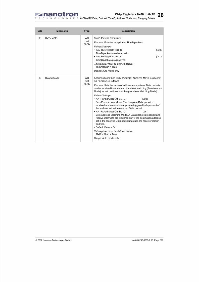
8/20/2019 nanoLOC NA5TR1 UserGuide
http://slidepdf.com/reader/full/nanoloc-na5tr1-userguide 245/325
Chip Registers 0x00 to 0x7F
0x5B – RX Data, Brdcast, TimeB, Address Mode, and Ranging Pulses
© 2007 Nanotron Technologies GmbH. NA-06-0230-0385-1.03 Page 229
26
2 RxTimeBEn WO
brst
BbClk
TIMEB P ACKET RECEPTION
Purpose: Enables reception of TimeB packets.
Values/Settings:
• NA_RxTimeBOff_BC_C (0x0)
TimeB packets are discarded.
• NA_RxTimeBOn_BC_C (0x1)
TimeB packets are received.
This register must be defined before:
RxCmdStart = True
Usage: Auto mode only.
3 RxAddrMode WO
brst
BbClk
ADDRESS MODE FOR D ATA P ACKETS: ADDRESS M ATCHING MODE
OR PROMISCUOUS MODE
Purpose: Sets the mode of address comparison. Data packets
can be received independent of address matching (Promiscuous
Mode), or with address matching (Address Matching Mode).
Values/Settings:
• NA_RxAddrModeOff_BC_C (0x0)
Sets Promiscuous Mode. The complete Data packet is
received and receive interrupts are triggered independent of
the address set in the received Data packet.
• NA_RxAddrModeOn_BC_C (0x1)
Sets Address Matching Mode. A Data packet is received and
receive interrupts are triggered only if the destination address
set in the received Data packet matches the receiver station
address.
• Default Value = 0x1
This register must be defined before:
RxCmdStart = TrueUsage: Auto mode only.
Bits Mnemonic Prop Description

8/20/2019 nanoLOC NA5TR1 UserGuide
http://slidepdf.com/reader/full/nanoloc-na5tr1-userguide 246/325
Chip Registers 0x00 to 0x7F
0x5C – Delay Detection Tuning
Page 230 NA-06-0230-0385-1.03 © 2007 Nanotron Technologies GmbH.
26
26.82 0x5C – Delay Detection Tuning
Used for tuning the delay in the correlator.
Write Only Fields
MSB Bit Number LSB
Offset RW 7 6 5 4 3 2 1 0
0x5C
R
init 0 0 0 0 0 0 0 0
W PulseDetDelay
init 0 0 0 0 0 1 0 1
Bits Mnemonic Prop Description
0-4 PulseDetDelay WO
brst
BbClk
DELAY TUNING FOR PULSE DETECTION
Purpose: Tunes the delay in the correlator.
Values/Settings:
• Default Value = 0x5

8/20/2019 nanoLOC NA5TR1 UserGuide
http://slidepdf.com/reader/full/nanoloc-na5tr1-userguide 247/325
Chip Registers 0x00 to 0x7F
0x5D – Receive Bit Detector Controls (Bit Detectors)
© 2007 Nanotron Technologies GmbH. NA-06-0230-0385-1.03 Page 231
26
26.83 0x5D – Receive Bit Detector Controls (Bit Detectors)
Used for disabling the detection of up pulses (Upchirps) and/or down pulses (Downchirps), and for setting
the required number of consecutive pulses needed to be outside of the gate center before a readjustment of
the gate occurs.
Write Only Fields
MSB Bit Number LSB
Offset RW 7 6 5 4 3 2 1 0
0x5D
R
init 0 0 0 0 0 0 0 0
W
Up
Pulse
Detect
Dis
Down
Pulse
Detect
Dis
GateAdjThreshold
init 0 0 0 0 0 1 1 1
Bits Mnemonic Prop Description
0-2 GateAdjThreshold WO
brst
BbClk
G ATE ADJUST THRESHOLD
Purpose: Because of clock drifting, the detected pulse can run
out of center of the gate. This sets the required number of con-
secutive pulses outside of the gate center before a readjust-
ment of the gate takes place.
Values/Settings:• Default Value = 0x7
This register must be defined before:
RxCmdStart = True
4 DownPulseDetectDis WO
brst
BbClk
DISABLE DETECTION OF DOWN PULSES
Purpose: Disables the detection of down pulses (Downchirps)
in the bit detector.
Values/Settings:
• 0 = Enable
• 1 = Disable
• Default Value = 0x0
5 UpPulseDetectDis WO
brst
BbClk
DISABLE DETECTION OF UP PULSES
Purpose: Disables the detection of up pulses (Upchirps) in the
bit detector.
Values/Settings:
• 0 = Enable
• 1 = Disable
• Default Value = 0x0

8/20/2019 nanoLOC NA5TR1 UserGuide
http://slidepdf.com/reader/full/nanoloc-na5tr1-userguide 248/325
Chip Registers 0x00 to 0x7F
0x5E – Bit Detection Gate Size and Adjustment
Page 232 NA-06-0230-0385-1.03 © 2007 Nanotron Technologies GmbH.
26
26.84 0x5E – Bit Detection Gate Size and Adjustment
Used for setting the size of the bit detection gate for unsynchronized state, for bit synchronization state, and
for frame synchronized state. It is also used for enabling the adjustment of the detection gate in bit synchro-
nization state and frame synchronization state.
Write Only Fields
MSB Bit Number LSB
Offset RW 7 6 5 4 3 2 1 0
0x5E
R
init 0 0 0 0 0 0 0 0
W
GateAdj
Frame
syncEn
GateAdj
Bitsync
En
GateSizeFramesync GateSizeBitsync GateSizeUnsync
init 1 1 0 1 0 1 0 1
Bits Mnemonic Prop Description
0-1 GateSizeUnsync WO
brst
BbClk
G ATE SIZE FOR UNSYNCHRONIZED STATE
Purpose: Sets the size of the detection gate in the baseband
clock cycles for the unsynchronized state.
Values/Settings:
• NA_GateSize3Slots_VC_C (0x0)
Sets gate size = 3 slots.
• NA_GateSize5Slots_VC_C (0x1)
Sets gate size = 5 slots.
• NA_GateSize7Slots_VC_C (0x2)
Sets gate size = 7 slots.
• NA_GateSize9Slots_VC_C (0x3)
Sets gate size = 9 slots.
• Default Value = 0x1
Note: 1 slot = 31.25 ns (one baseband clock cycle).
This register must be defined before:
RxCmdStart = True
2-3 GateSizeBitsync WO
brst
BbClk
G ATE SIZE FOR BIT SYNCHRONIZATION STATE
Purpose: Sets the size of the detection gate in baseband clock
cycles for the bit synchronization state.
Values/Settings:
• NA_GateSize3Slots_VC_C (0x0)
Sets gate size = 3 slots.
• NA_GateSize5Slots_VC_C (0x1)
Sets gate size = 5 slots.
• NA_GateSize7Slots_VC_C (0x2)
Sets gate size = 7 slots.
• NA_GateSize9Slots_VC_C (0x3)
Sets gate size = 9 slots.
• Default Value = 0x1
Note: 1 slot = 31.25 ns (one baseband clock cycle).
This register must be defined before:
RxCmdStart = True

8/20/2019 nanoLOC NA5TR1 UserGuide
http://slidepdf.com/reader/full/nanoloc-na5tr1-userguide 249/325
Chip Registers 0x00 to 0x7F
0x5E – Bit Detection Gate Size and Adjustment
© 2007 Nanotron Technologies GmbH. NA-06-0230-0385-1.03 Page 233
26
4-5 GateSizeFramesync WO
brst
BbClk
G ATE SIZE FOR FRAME SYNCHRONIZATION STATE
Purpose: Sets the size of the detection gate in baseband clock
cycles for the frame synchronization state.
Values/Settings:
• NA_GateSize3Slots_VC_C (0x0)
Sets gate size = 3 slots.
• NA_GateSize5Slots_VC_C (0x1)
Sets gate size = 5 slots.
• NA_GateSize7Slots_VC_C (0x2)
Sets gate size = 7 slots.
• NA_GateSize9Slots_VC_C (0x3)
Sets gate size = 9 slots.
• Default Value = 0x1
Note: 1 slot = 31.25 ns (one baseband clock cycle).
This register must be defined before:
RxCmdStart = True
6 GateAdjBitsyncEn WO
brst
BbClk
DETECTION G ATE ADJUSTMENT FOR BIT SYNCHRONIZATION STATE
Purpose: Enables gate adjustment in bit synchronization state.
Values/Settings:
• 0 = Disable
• 1 = Enable
• Default Value = 0x1
7 GateAdjFramesyncEn WO
brst
BbClk
DETECTION G ATE ADJUSTMENT FOR FRAME SYNCHRONIZATION
STATE
Purpose: Enables gate adjustment in frame synchronization
state.Values/Settings:
• 0 = Disable
• 1 = Enable
• Default Value = 0x1
Note: GateAdjFramesyncEn must be disabled for Ranging.
Bits Mnemonic Prop Description

8/20/2019 nanoLOC NA5TR1 UserGuide
http://slidepdf.com/reader/full/nanoloc-na5tr1-userguide 250/325
Chip Registers 0x00 to 0x7F
0x5F – Bit Synchronization/Unsynchronization Thresholds
Page 234 NA-06-0230-0385-1.03 © 2007 Nanotron Technologies GmbH.
26
26.85 0x5F – Bit Synchronization/Unsynchronization Thresholds
Used for setting the threshold (number of consecutive detected chirp pulses) to enter bit synchronization
state from the unsynchronized state, as well as for setting the threshold (number of consecutive lost chirp
pulses) to enter the unsynchronized state from bit synchronization state.
Note: The frame synchronization state is reached after the SyncWord has been received.
Write Only Fields
MSB Bit Number LSB
Offset RW 7 6 5 4 3 2 1 0
0x5F
R
init 0 0 0 0 0 0 0 0
W LeaveBitsyncThreshold Go2BitsyncThreshold
init 0 1 1 0 0 0 1 0
Bits Mnemonic Prop Description
0-2 Go2BitsyncThreshold WO
brst
BbClk
THRESHOLD FOR ENTERING BIT SYNCHRONIZATION
Purpose: Sets the required number of consecutive chirp pulses
detected in the unsynchronized state to go to bit synchroniza-
tion state.
Values/Settings:
• Default Value = 0x2
This register must be defined before:RxCmdStart = True
4-6 LeaveBitsyncThreshold WO
brst
BbClk
THRESHOLD FOR LEAVING BIT SYNCHRONIZATION
Purpose: Sets the required number of consecutive non-
detected chirp pulses (lost pulses) in bit synchronization state
to return to the unsynchronized state.
Values/Settings:
• Default Value = 0x6
This register must be defined before:
RxCmdStart = True

8/20/2019 nanoLOC NA5TR1 UserGuide
http://slidepdf.com/reader/full/nanoloc-na5tr1-userguide 251/325
Chip Registers 0x00 to 0x7F
0x60 – Real Time Clock TimeB Transmission Delay Adjustment
© 2007 Nanotron Technologies GmbH. NA-06-0230-0385-1.03 Page 235
26
26.86 0x60 – Real Time Clock TimeB Transmission Delay Adjustment
Used for adjusting the RTC values before transmission due to hardware delays inside the transmitter.
Write Only Fields
MSB Bit Number LSB
Offset RW 7 6 5 4 3 2 1 0
0x60
R
init 0 0 0 0 0 0 0 0
W RtcTimeBTxAdj
init 0 0 0 0 0 0 0 0
Bits Mnemonic Prop Description
0-7 RtcTimeBTxAdj WO
brst
BbClk
REAL TIME CLOCK TIMEB TRANSMISSION DELAY ADJUSTMENT
Purpose: Before transmitting, the Real Time Clock control value is adjusted
to compensate for transmitter delays.
• NA_MacRtcTimeBTxAdj1M2Ary_IC_C (0x05)
Adjustment for 1 Msymbols 2Ary.
• NA_MacRtcTimeBTxAdj1M2AryFec_IC_C (0x07)
Adjustment for 1 Msymbols 2Ary FEC.
• NA_MacRtcTimeBTxAdj500k2Ary_IC_C (0x09)
Adjustment for 500 ksymbols 2Ary.
• NA_MacRtcTimeBTxAdj500k2AryFec_IC_C (0x0F)
Adjustment for 500 ksymbols 2Ary FEC.
• Default Value = 0x0
Note: This value is added to the RTC value after reading due to the delay in
the transmitter while shifting out this value.
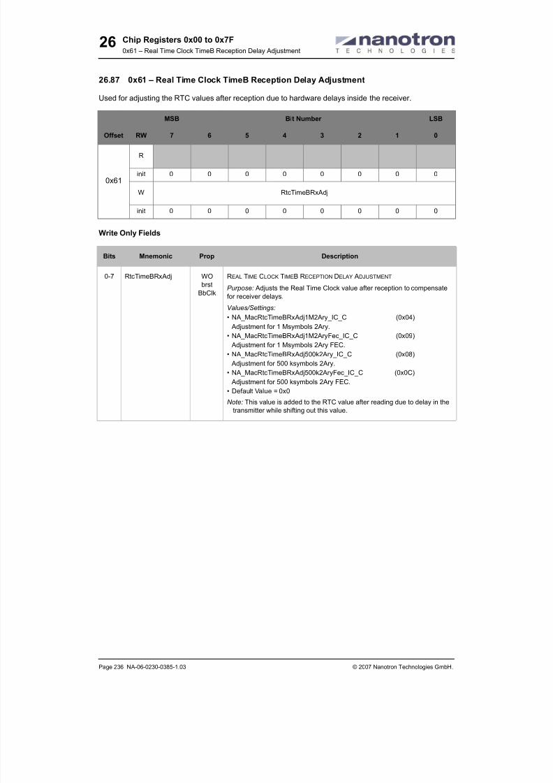
8/20/2019 nanoLOC NA5TR1 UserGuide
http://slidepdf.com/reader/full/nanoloc-na5tr1-userguide 252/325
Chip Registers 0x00 to 0x7F
0x61 – Real Time Clock TimeB Reception Delay Adjustment
Page 236 NA-06-0230-0385-1.03 © 2007 Nanotron Technologies GmbH.
26
26.87 0x61 – Real Time Clock TimeB Reception Delay Adjustment
Used for adjusting the RTC values after reception due to hardware delays inside the receiver.
Write Only Fields
MSB Bit Number LSB
Offset RW 7 6 5 4 3 2 1 0
0x61
R
init 0 0 0 0 0 0 0 0
W RtcTimeBRxAdj
init 0 0 0 0 0 0 0 0
Bits Mnemonic Prop Description
0-7 RtcTimeBRxAdj WO
brst
BbClk
REAL TIME CLOCK TIMEB RECEPTION DELAY ADJUSTMENT
Purpose: Adjusts the Real Time Clock value after reception to compensate
for receiver delays.
Values/Settings:
• NA_MacRtcTimeBRxAdj1M2Ary_IC_C (0x04)
Adjustment for 1 Msymbols 2Ary.
• NA_MacRtcTimeBRxAdj1M2AryFec_IC_C (0x09)
Adjustment for 1 Msymbols 2Ary FEC.
• NA_MacRtcTimeBRxAdj500k2Ary_IC_C (0x08)
Adjustment for 500 ksymbols 2Ary.
• NA_MacRtcTimeBRxAdj500k2AryFec_IC_C (0x0C) Adjustment for 500 ksymbols 2Ary FEC.
• Default Value = 0x0
Note: This value is added to the RTC value after reading due to delay in the
transmitter while shifting out this value.
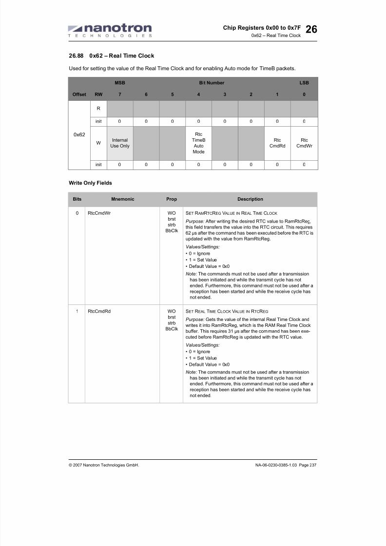
8/20/2019 nanoLOC NA5TR1 UserGuide
http://slidepdf.com/reader/full/nanoloc-na5tr1-userguide 253/325
Chip Registers 0x00 to 0x7F
0x62 – Real Time Clock
© 2007 Nanotron Technologies GmbH. NA-06-0230-0385-1.03 Page 237
26
26.88 0x62 – Real Time Clock
Used for setting the value of the Real Time Clock and for enabling Auto mode for TimeB packets.
Write Only Fields
MSB Bit Number LSB
Offset RW 7 6 5 4 3 2 1 0
0x62
R
init 0 0 0 0 0 0 0 0
WInternal
Use Only
Rtc
TimeB
Auto
Mode
Rtc
CmdRd
Rtc
CmdWr
init 0 0 0 0 0 0 0 0
Bits Mnemonic Prop Description
0 RtcCmdWr WO
brst
strb
BbClk
SET R AMRTCREG V ALUE IN REAL TIME CLOCK
Purpose: After writing the desired RTC value to RamRtcReg,
this field transfers the value into the RTC circuit. This requires
62 µs after the command has been executed before the RTC is
updated with the value from RamRtcReg.
Values/Settings:
• 0 = Ignore
• 1 = Set Value• Default Value = 0x0
Note: The commands must not be used after a transmission
has been initiated and while the transmit cycle has not
ended. Furthermore, this command must not be used after a
reception has been started and while the receive cycle has
not ended.
1 RtcCmdRd WO
brst
strb
BbClk
SET REAL TIME CLOCK V ALUE IN RTCREG
Purpose: Gets the value of the internal Real Time Clock and
writes it into RamRtcReg, which is the RAM Real Time Clock
buffer. This requires 31 µs after the command has been exe-
cuted before RamRtcReg is updated with the RTC value.
Values/Settings:• 0 = Ignore
• 1 = Set Value
• Default Value = 0x0
Note: The commands must not be used after a transmission
has been initiated and while the transmit cycle has not
ended. Furthermore, this command must not be used after a
reception has been started and while the receive cycle has
not ended.

8/20/2019 nanoLOC NA5TR1 UserGuide
http://slidepdf.com/reader/full/nanoloc-na5tr1-userguide 254/325
Chip Registers 0x00 to 0x7F
0x62 – Real Time Clock
Page 238 NA-06-0230-0385-1.03 © 2007 Nanotron Technologies GmbH.
26
4 RtcTimeBAutoMode WO
brst
BbClk
REAL TIME CLOCK AUTO MODE FOR TIMEB P ACKETS
Purpose: Automatically sets the RTC values in TimeB packets
for transmission and automatically stores the RTC values ofreceived TimeB packets in the RTC. Otherwise, the RTC val-
ues in TimeB packets for transmission are taken from RAM in
RamRtcTx and the RTC values in received TimeB packets is
stored in RamRtcRx.
Values/Settings:
• NA_RtcTimeBAutoModeOff_BC_C(0x0)
The value of RamRtcTx is transmitted in the RTC field of the
TimeB packet, while the RTC value in a received TimeB
packet is stored in RamRtcRx.
• NA_RtcTimeBAutoModeOn_BC_C(0x1)
The RTC value for a transmitted TimeB packet is taken from
the Real Time Clock, while the RTC value from a received
TimeB is automatically stored in the Real Time Clock.
• Default Value = 0x0
Bits Mnemonic Prop Description

8/20/2019 nanoLOC NA5TR1 UserGuide
http://slidepdf.com/reader/full/nanoloc-na5tr1-userguide 255/325
Chip Registers 0x00 to 0x7F
0x63 – AGC Amplitude
© 2007 Nanotron Technologies GmbH. NA-06-0230-0385-1.03 Page 239
26
26.89 0x63 – AGC Amplitude
Used in the alternative AGC to change gain value of the desired amplitude.
Write Only Fields
MSB Bit Number LSB
Offset RW 7 6 5 4 3 2 1 0
0x63
R
init 0 0 0 0 0 0 0 0
W AgcAmplitude
init 0 0 0 0 1 1 0 0
Bits Mnemonic Prop Description
0-4 AgcAmplitude WO AGC AMPLITUDE
Purpose: Select desired Amplitude for alternative AGC.
Values/Settings:
• Default Value = 0x0

8/20/2019 nanoLOC NA5TR1 UserGuide
http://slidepdf.com/reader/full/nanoloc-na5tr1-userguide 256/325
Chip Registers 0x00 to 0x7F
0x64 – Alternative AGC and AGC Range Offset
Page 240 NA-06-0230-0385-1.03 © 2007 Nanotron Technologies GmbH.
26
26.90 0x64 – Alternative AGC and AGC Range Offset
Used for switching between standard AGC and alternate AGC and for setting the value in AgcRangeOffset.
Write Fields
MSB Bit Number LSB
Offset RW 7 6 5 4 3 2 1 0
0x64
R
init 0 0 0 0 0 0 0 0
W
Use
Alter
native
Agc
AgcRangeOffset
init 0 0 0 0 1 0 1 0
Bits Mnemonic Prop Description
0-3 AgcRangeOffset WO AGC R ANGE OFFSET
Purpose: Sets a value in AgcRangeOffset so that the AGC is
temporarily halted when:
| Mean Value - Middle | > AgcRangeOffset
Values/Settings:
• Default Value = 0x0
7 UseAlternativeAgc WO USE ALTERNATIVE AGC
Purpose: Switches between the standard and alternative AGC.
Values/Settings:
• 0 = Disable
• 1 = Enable
• Default Value = 0x0
Note: Do not switch between AGCs when the receiver is run-
ning.

8/20/2019 nanoLOC NA5TR1 UserGuide
http://slidepdf.com/reader/full/nanoloc-na5tr1-userguide 257/325
Chip Registers 0x00 to 0x7F
0x65 to 0x7C – Reserved Registers
© 2007 Nanotron Technologies GmbH. NA-06-0230-0385-1.03 Page 241
26
26.91 0x65 to 0x7C – Reserved Registers
Registers between 0x65 and 0x7C inclusive are reserved. The default value for all fields in these registers is
0x0.
MSB Bit Number LSB
Offset RW 7 6 5 4 3 2 1 0
0x65
R
init 0 0 0 0 0 0 0 0
W
init 0 0 0 0 0 0 0 0
0x7C
R
init 0 0 0 0 0 0 0 0
W
init 0 0 0 0 0 0 0 0
.
..

8/20/2019 nanoLOC NA5TR1 UserGuide
http://slidepdf.com/reader/full/nanoloc-na5tr1-userguide 258/325
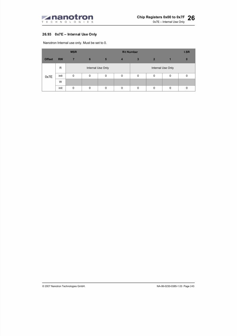
8/20/2019 nanoLOC NA5TR1 UserGuide
http://slidepdf.com/reader/full/nanoloc-na5tr1-userguide 259/325
Chip Registers 0x00 to 0x7F
0x7E – Internal Use Only
© 2007 Nanotron Technologies GmbH. NA-06-0230-0385-1.03 Page 243
26
26.93 0x7E – Internal Use Only
Nanotron Internal use only. Must be set to 0.
MSB Bit Number LSB
Offset RW 7 6 5 4 3 2 1 0
0x7E
R Internal Use Only Internal Use Only
init 0 0 0 0 0 0 0 0
W
init 0 0 0 0 0 0 0 0

8/20/2019 nanoLOC NA5TR1 UserGuide
http://slidepdf.com/reader/full/nanoloc-na5tr1-userguide 260/325
Chip Registers 0x00 to 0x7F
0x7F – Internal Use Only
Page 244 NA-06-0230-0385-1.03 © 2007 Nanotron Technologies GmbH.
26
26.94 0x7F – Internal Use Only
Nanotron Internal use only. Must be set to 0.
MSB Bit Number LSB
Offset RW 7 6 5 4 3 2 1 0
0x7F
R Internal Use OnlyInternal
Use Only
Internal
Use OnlyInternal Use Only
init 0 0 0 0 0 0 0 0
W
init 0 0 0 0 0 0 0 0

8/20/2019 nanoLOC NA5TR1 UserGuide
http://slidepdf.com/reader/full/nanoloc-na5tr1-userguide 261/325
Memory Map of Baseband RAM Locations
nanoLOC TRX Transceiver (NA5TR1) User Guide
© 2008 Nanotron Technologies GmbH. NA-06-0230-0385-2.00 Page 245
27
27 Memory Map of Baseband RAM Locations
The following tables describe the memory locations of the baseband RAM.
Note: All registers in baseband RAM are both readable and writable.
27.1 Auto/Duplex Mode
27.1.1 Auto/Duplex Page 0
Offset MSB Bit Number LSB
From To RW 7 6 5 4 3 2 1 0
0x80 0x85R
RamStaAddr0W
0x86 0x87
R
W
0x88 0x8DR
RamStaAddr1W
0x8E 0x8FR
W
0x90 0x95R
RamTxDstAddr W
0x96 0x97R
W
0x98 0x98R
RamTxLengthW
0x99 0x99R
RamTx
LCh
RamTx
SeqN
RamTx
FragCRamTxLength
W
0x9A 0xA7R
W
0xA8 0xADR
RamRxDstAddr
W
0xAE 0xAFR
W
0xB0 0xB5R
RamRxSrcAddr W
0xB6 0xB7R
W
0xB8 0xB8R
RamRxLengthW

8/20/2019 nanoLOC NA5TR1 UserGuide
http://slidepdf.com/reader/full/nanoloc-na5tr1-userguide 262/325
Memory Map of Baseband RAM Locations
nanoLOC TRX Transceiver (NA5TR1) User Guide
Page 246 NA-06-0230-0385-2.00 © 2008 Nanotron Technologies GmbH.
27
27.1.2 Auto/Duplex Page 1
0xB9 0xB9
R
RamRx-LCh RamRx-SeqN RamRx-FragC RamRxLengthW
0xBA 0xDFR
W
0xE0 0xE5R
RamRtcTxW
0xE6 0xE7R
W
0xE8 0xED
R
RamRtcRxW
0xEE 0xEFR
W
0xF0 0xFFR
RamRtcRegW
Offset MSB Bit Number LSB
From To RW 7 6 5 4 3 2 1 0
Register SpaceR
W
0x180 0x18FR
RamTxRxCryptKeyW
0x190 0x1BFR
W
0x1C0 0x1CFR
RamTxCryptClockW
0x1D0 0x1DFR
W
0x1E0 0x1EFR
RamRxCryptClockW
0x1F0 0x1FFR
W
Offset MSB Bit Number LSB
From To RW 7 6 5 4 3 2 1 0

8/20/2019 nanoLOC NA5TR1 UserGuide
http://slidepdf.com/reader/full/nanoloc-na5tr1-userguide 263/325
Memory Map of Baseband RAM Locations
nanoLOC TRX Transceiver (NA5TR1) User Guide
© 2008 Nanotron Technologies GmbH. NA-06-0230-0385-2.00 Page 247
27
27.1.3 Auto/Duplex Page 2
27.1.4 Auto/Duplex Page 3
Offset MSB Bit Number LSB
From To RW 7 6 5 4 3 2 1 0
Register SpaceR
W
0x280 0x2FFR
RamRxBuffer W
MSB Bit Number LSB
Offset RW 7 6 5 4 3 2 1 0
Register SpaceR
W
0x380 0x3FFR
RamTxBuffer W

8/20/2019 nanoLOC NA5TR1 UserGuide
http://slidepdf.com/reader/full/nanoloc-na5tr1-userguide 264/325
Memory Map of Baseband RAM Locations
nanoLOC TRX Transceiver (NA5TR1) User Guide
Page 248 NA-06-0230-0385-2.00 © 2008 Nanotron Technologies GmbH.
27
27.2 Auto/Simplex Mode
27.2.1 Auto/Simplex Page 0
Same as Auto/Duplex Page 0 on page 245.
27.2.2 Auto/Simplex Page 1
Same as Auto/Duplex Page 1 on page 246.
27.2.3 Auto/Simplex Pages 2 and 3
Offset MSB Bit Number LSB
From To RW 7 6 5 4 3 2 1 0
0x280 0x2FFR
RamTxRxBuffer W
0x380 0x3FFR
RamTxRxBuffer W

8/20/2019 nanoLOC NA5TR1 UserGuide
http://slidepdf.com/reader/full/nanoloc-na5tr1-userguide 265/325
Memory Map of Baseband RAM Locations
nanoLOC TRX Transceiver (NA5TR1) User Guide
© 2008 Nanotron Technologies GmbH. NA-06-0230-0385-2.00 Page 249
27
27.3 Transparent/Duplex Mode
27.3.1 Transparent/Duplex Pages 0 and 1
27.3.2 Transparent/Duplex Pages 2 and 3
Offset MSB Bit Number LSB
From To RW 7 6 5 4 3 2 1 0
0x080 0x0FFR
RamRxTransBuffer W
0x180 0x1FFR
RamRxTransBuffer W
Offset MSB Bit Number LSB
From To RW 7 6 5 4 3 2 1 0
0x280 0x2FFR
RamTxTransBuffer W
0x380 0x3FFR
RamTxTransBuffer W

8/20/2019 nanoLOC NA5TR1 UserGuide
http://slidepdf.com/reader/full/nanoloc-na5tr1-userguide 266/325
Memory Map of Baseband RAM Locations
nanoLOC TRX Transceiver (NA5TR1) User Guide
Page 250 NA-06-0230-0385-2.00 © 2008 Nanotron Technologies GmbH.
27
27.4 Transparent/Simplex Mode
Transparent/Simplex Pages 0, 1, 2, and 3
Offset MSB Bit Number LSB
From To RW 7 6 5 4 3 2 1 0
0x080 0x0FFR
RamTxRxTransBuffer W
0x180 0x1FFR
RamTxRxTransBuffer W
0x280 0x2FFR
RamTxRxTransBuffer W
0x380 0x3FF
R
RamTxRxTransBuffer W

8/20/2019 nanoLOC NA5TR1 UserGuide
http://slidepdf.com/reader/full/nanoloc-na5tr1-userguide 267/325
Baseband RAM Locations: 0x80 to 0x3FF
Auto/Duplex [Pg 0] 0x80 to 0x85 – Source Station Address 0
© 2008 Nanotron Technologies GmbH. NA-06-0230-0385-2.00 Page 251
28
28 Baseband RAM Locations: 0x80 to 0x3FF
28.1 Auto/Duplex [Pg 0] 0x80 to 0x85 – Source Station Address 0
Used to buffer the 48 bit address of the source station based on the IEEE standard addressing convention.
The first 24 bits correspond to the Organizationally Unique Identifier assigned by IEEE, while the second 24
bits are administered locally. This address is set in the MACFrame of a Data, Brdcast, TimeB, and Reg2S
packet.
Read/Write
Offset MSB Bit Number LSB
From To RW 7 6 5 4 3 2 1 0
0x80 0x85R
RamStaAddr0W
Bits Mnemonic Prop Description
0-47 RamStaAddr0 RW
brst
BbClk
RAM
STATION ADDRESS B ASED ON IEEE ADDRESSING CONVENTION
Purpose: Stores a 48 bit universally administered IEEE
address of the source station.
Register Values/Settings:
• If this convention is used, then set the first two bits of this field
as follows:
• RamStaAddr0[0] = 0
• RamStaAddr0[1] = 0
• Default Value = 0x0
Note: It is not mandatory to use this convention for addressing.

8/20/2019 nanoLOC NA5TR1 UserGuide
http://slidepdf.com/reader/full/nanoloc-na5tr1-userguide 268/325
Baseband RAM Locations: 0x80 to 0x3FF
Auto/Duplex [Pg 0] 0x86 to 0x87 – Reserved
Page 252 NA-06-0230-0385-2.00 © 2008 Nanotron Technologies GmbH.
28
28.2 Auto/Duplex [Pg 0] 0x86 to 0x87 – Reserved
These RAM locations are reserved.
Offset MSB Bit Number LSB
From To RW 7 6 5 4 3 2 1 0
0x86 0x87R
ReservedW
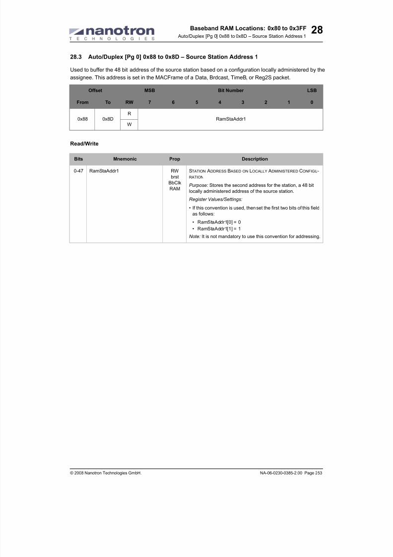
8/20/2019 nanoLOC NA5TR1 UserGuide
http://slidepdf.com/reader/full/nanoloc-na5tr1-userguide 269/325
Baseband RAM Locations: 0x80 to 0x3FF
Auto/Duplex [Pg 0] 0x88 to 0x8D – Source Station Address 1
© 2008 Nanotron Technologies GmbH. NA-06-0230-0385-2.00 Page 253
28
28.3 Auto/Duplex [Pg 0] 0x88 to 0x8D – Source Station Address 1
Used to buffer the 48 bit address of the source station based on a configuration locally administered by the
assignee. This address is set in the MACFrame of a Data, Brdcast, TimeB, or Reg2S packet.
Read/Write
Offset MSB Bit Number LSB
From To RW 7 6 5 4 3 2 1 0
0x88 0x8DR
RamStaAddr1W
Bits Mnemonic Prop Description
0-47 RamStaAddr1 RW
brstBbClk
RAM
STATION ADDRESS B ASED ON LOCALLY ADMINISTERED CONFIGU-
RATION
Purpose: Stores the second address for the station, a 48 bit
locally administered address of the source station.
Register Values/Settings:
• If this convention is used, then set the first two bits of this field
as follows:
• RamStaAddr1[0] = 0
• RamStaAddr1[1] = 1
Note: It is not mandatory to use this convention for addressing.

8/20/2019 nanoLOC NA5TR1 UserGuide
http://slidepdf.com/reader/full/nanoloc-na5tr1-userguide 270/325
Baseband RAM Locations: 0x80 to 0x3FF
Auto/Duplex [Pg 0] 0x8E to 0x8F – Reserved
Page 254 NA-06-0230-0385-2.00 © 2008 Nanotron Technologies GmbH.
28
28.4 Auto/Duplex [Pg 0] 0x8E to 0x8F – Reserved
These RAM locations are reserved.
Offset MSB Bit Number LSB
From To RW 7 6 5 4 3 2 1 0
0x86 0x87R
ReservedW

8/20/2019 nanoLOC NA5TR1 UserGuide
http://slidepdf.com/reader/full/nanoloc-na5tr1-userguide 271/325
Baseband RAM Locations: 0x80 to 0x3FF
Auto/Duplex [Pg 0] 0x90 to 0x95 – TX Destination Address
© 2008 Nanotron Technologies GmbH. NA-06-0230-0385-2.00 Page 255
28
28.5 Auto/Duplex [Pg 0] 0x90 to 0x95 – TX Destination Address
Used to buffer a 48 bit address of the destination station to be set in the MACFrame of a Data or Brdcast
packet that is to be transmitted. This destination address is used in all packet types, except the TimeB
packet. In TimeB packets, this RAM location contains a Real Time Clock value.
Read/Write
Offset MSB Bit Number LSB
From To RW 7 6 5 4 3 2 1 0
0x90 0x95R
RamTxDstAddr W
Bits Mnemonic Prop Description
0-47 RamTxDstAddr RWbrst
BbClk
RAM
TRANSMIT DESTINATION ADDRESS
Purpose: Stores the 48 bit address of the destination station for
a Data packet that is to be transmitted, as well as the 48 bit
broadcast/ multicast address of a Brdcast packet to be trans-
mitted.
Register Values/Settings:
• Default Value = 0x0
This register must be defined before:
TxCmdStart = True.
Usage: Auto mode only.

8/20/2019 nanoLOC NA5TR1 UserGuide
http://slidepdf.com/reader/full/nanoloc-na5tr1-userguide 272/325
Baseband RAM Locations: 0x80 to 0x3FF
Auto/Duplex [Pg 0] 0x96 to 0x97 – Reserved
Page 256 NA-06-0230-0385-2.00 © 2008 Nanotron Technologies GmbH.
28
28.6 Auto/Duplex [Pg 0] 0x96 to 0x97 – Reserved
These RAM locations are reserved.
Offset MSB Bit Number LSB
From To RW 7 6 5 4 3 2 1 0
0x96 0x97R
ReservedW

8/20/2019 nanoLOC NA5TR1 UserGuide
http://slidepdf.com/reader/full/nanoloc-na5tr1-userguide 273/325
Baseband RAM Locations: 0x80 to 0x3FF
Auto/Duplex [Pg 0] 0x98 to 0x99 – TX Data Length and Bits for SW Us-
© 2008 Nanotron Technologies GmbH. NA-06-0230-0385-2.00 Page 257
28
28.7 Auto/Duplex [Pg 0] 0x98 to 0x99 – TX Data Length and Bits for SW Usage
Used to set the length of the data field in packets to be transmitted, as well as to set three bits that are avail-
able for use by software.
Read/Write
Offset MSB Bit Number LSB
From To RW 7 6 5 4 3 2 1 0
0x98 0x98R
RamTxLengthW
0x99 0x99
RRamTxFragC
TX Transparent Bits
for SW usage
RamTxLengthW
Bits Mnemonic Prop Description
0-12 RamTxLength RW
brst
BbClk
RAM
D ATA FIELD LENGTH OF A P ACKET TO BE TRANSMITTED
Purpose: Sets the number of bytes of the Data field of Data,
Brdcast, and TimeB packets. This field will also be transmitted
in a Req2s packet when using 3-way handshaking.
Register Values/Settings:
• Default Value = 0x0
This register must be defined before:
TxCmdStart = True.
Usage: Auto mode only.
13-15 RamTxFragC RWbrst
BbClk
RAM
These bits are transparent for the nanoLOC. There are onlyloaded from RAM together with the TxLength field and sent in
the MACFrame. On the receiver side they can be read from the
corresponding RX field called “RX Transparent Bits for SW
usage.”
In several applications these bits were used on software level
to implement functionalities such as Link Control Channel, a
sequential numbering scheme, or a packet fragmentation
scheme.
See also: Auto/Duplex [Pg 0] 0xB8 to 0xB9 – RX Data Length
and Bits for SW Usage (see page 263).
Usage: Auto mode only.
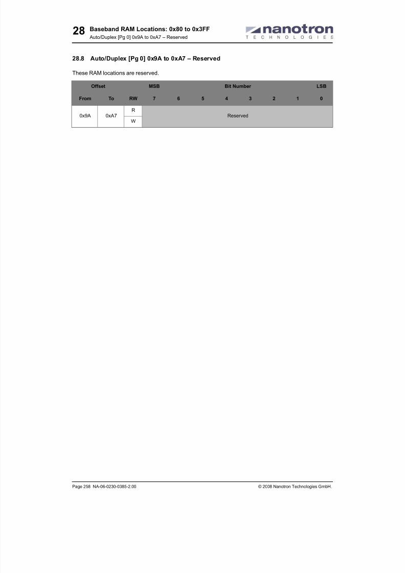
8/20/2019 nanoLOC NA5TR1 UserGuide
http://slidepdf.com/reader/full/nanoloc-na5tr1-userguide 274/325
Baseband RAM Locations: 0x80 to 0x3FF
Auto/Duplex [Pg 0] 0x9A to 0xA7 – Reserved
Page 258 NA-06-0230-0385-2.00 © 2008 Nanotron Technologies GmbH.
28
28.8 Auto/Duplex [Pg 0] 0x9A to 0xA7 – Reserved
These RAM locations are reserved.
Offset MSB Bit Number LSB
From To RW 7 6 5 4 3 2 1 0
0x9A 0xA7R
ReservedW

8/20/2019 nanoLOC NA5TR1 UserGuide
http://slidepdf.com/reader/full/nanoloc-na5tr1-userguide 275/325
Baseband RAM Locations: 0x80 to 0x3FF
Auto/Duplex [Pg 0] 0xA8 to 0xAD – RX Destination Address
© 2008 Nanotron Technologies GmbH. NA-06-0230-0385-2.00 Page 259
28
28.9 Auto/Duplex [Pg 0] 0xA8 to 0xAD – RX Destination Address
Used to buffer the 48 bit address of the destination address field provided in the MACFrame of a received
Data or Brdcast packet.
Read/Write
Offset MSB Bit Number LSB
From To RW 7 6 5 4 3 2 1 0
0xA8 0xADR
RamRxDstAddr W
Bits Mnemonic Prop Description
0-47 RamRxDstAddr RW
brstBbClk
RAM
RECEIVE DESTINATION ADDRESS
Purpose: Stores the destination address from received Data
and Brdcast packets. It allows for the retrieval of the destina-
tion address when in promiscuous mode in order to compare
broadcast/multicast addresses (Brdcast packets).
Register Values/Settings:
• Default Value = 0x0
Note: Valid when:
• RxHeaderEnd event is triggered
• RxCrc1 == RxCrc1Succ
• RxPacketType == RxPacketTypeData |
RxPacketTypeBrdcast
Usage: Auto mode only.

8/20/2019 nanoLOC NA5TR1 UserGuide
http://slidepdf.com/reader/full/nanoloc-na5tr1-userguide 276/325
Baseband RAM Locations: 0x80 to 0x3FF
Auto/Duplex [Pg 0] 0xAE to 0xAF – Reserved
Page 260 NA-06-0230-0385-2.00 © 2008 Nanotron Technologies GmbH.
28
28.10 Auto/Duplex [Pg 0] 0xAE to 0xAF – Reserved
These RAM locations are reserved.
Offset MSB Bit Number LSB
From To RW 7 6 5 4 3 2 1 0
0xAE 0xAFR
ReservedW

8/20/2019 nanoLOC NA5TR1 UserGuide
http://slidepdf.com/reader/full/nanoloc-na5tr1-userguide 277/325
Baseband RAM Locations: 0x80 to 0x3FF
Auto/Duplex [Pg 0] 0xB0 to 0xB5 – RX Source Address
© 2008 Nanotron Technologies GmbH. NA-06-0230-0385-2.00 Page 261
28
28.11 Auto/Duplex [Pg 0] 0xB0 to 0xB5 – RX Source Address
Used to buffer the 48 bit address of the source address field provided in the MACFrame of a received Data
or Brdcast packet.
Read/Write
Offset MSB Bit Number LSB
From To RW 7 6 5 4 3 2 1 0
0xB0 0xB5R
RamRxSrcAddr W
Bits Mnemonic Prop Description
0-7 RamRxSrcAddr RW
brstBbClk
RAM
RECEIVE SOURCE ADDRESS
Purpose: Stores the source address of the received Data or
Brdcast packet.
Register Values/Settings:
• Default Value = 0x0
Note: Valid when:
• RxHeaderEnd event is triggered
• RxCrc1 == RxCrc1Succ
Usage: Auto mode only.

8/20/2019 nanoLOC NA5TR1 UserGuide
http://slidepdf.com/reader/full/nanoloc-na5tr1-userguide 278/325
Baseband RAM Locations: 0x80 to 0x3FF
Auto/Duplex [Pg 0] 0xB6 to 0xB7 – Reserved
Page 262 NA-06-0230-0385-2.00 © 2008 Nanotron Technologies GmbH.
28
28.12 Auto/Duplex [Pg 0] 0xB6 to 0xB7 – Reserved
These RAM locations are reserved.
Offset MSB Bit Number LSB
From To RW 7 6 5 4 3 2 1 0
0xB6 0xB7R
ReservedW

8/20/2019 nanoLOC NA5TR1 UserGuide
http://slidepdf.com/reader/full/nanoloc-na5tr1-userguide 279/325
Baseband RAM Locations: 0x80 to 0x3FF
Auto/Duplex [Pg 0] 0xB8 to 0xB9 – RX Data Length and Bits for SW
© 2008 Nanotron Technologies GmbH. NA-06-0230-0385-2.00 Page 263
28
28.13 Auto/Duplex [Pg 0] 0xB8 to 0xB9 – RX Data Length and Bits for SW Usage
Used to store a value which indicates the length of the data field in received packets, as well as to store
three bits that are available for use by software.
Read/Write
Offset MSB Bit Number LSB
From To RW 7 6 5 4 3 2 1 0
0xB8 0xB8R
RamRxLengthW
0xB9 0xB9
RRamRxFragC
RX Transparent Bits for SW
usage
RamRxLengthW
Bits Mnemonic Prop Description
0-12 RamRxLength RW
brst
BbClk
RAM
D ATA FIELD LENGTH OF RECEIVED P ACKET
Purpose: Stores the length (number of bytes) of the data field
of Data, Brdcast, TimeB, Req2S, and Clr2S packets.
Note: Valid when:
• RxHeaderEnd event is triggered
• RxCrc1 == RxCrc1Succ
Usage: Auto mode only
13-15 RamRxFragC RW
brst
BbClkRAM
These bits are transparent for the nanoLOC. They are only
stored to RAM together with the RxLength field received in the
MACFrame.In several applications these bits were used on software level
to implement functionalities such as Link Control Channel, a
sequential numbering scheme, or a packet fragmentation
scheme.
Usage: Auto mode only.

8/20/2019 nanoLOC NA5TR1 UserGuide
http://slidepdf.com/reader/full/nanoloc-na5tr1-userguide 280/325
Baseband RAM Locations: 0x80 to 0x3FF
Auto/Duplex [Pg 0] 0xBA to 0xDF – Reserved
Page 264 NA-06-0230-0385-2.00 © 2008 Nanotron Technologies GmbH.
28
28.14 Auto/Duplex [Pg 0] 0xBA to 0xDF – Reserved
These RAM locations are reserved.
Offset MSB Bit Number LSB
From To RW 7 6 5 4 3 2 1 0
0xBA 0xDFR
ReservedW

8/20/2019 nanoLOC NA5TR1 UserGuide
http://slidepdf.com/reader/full/nanoloc-na5tr1-userguide 281/325
Baseband RAM Locations: 0x80 to 0x3FF
Auto/Duplex [Pg 0] 0xE0 to 0xE5 – TX Real Time Clock Buffer
© 2008 Nanotron Technologies GmbH. NA-06-0230-0385-2.00 Page 265
28
28.15 Auto/Duplex [Pg 0] 0xE0 to 0xE5 – TX Real Time Clock Buffer
Used to temporarily buffer the 48 bit value of the Real Time Clock to prepare time beacon (TimeB) packets
for transmission.
Read/Write
Offset MSB Bit Number LSB
From To RW 7 6 5 4 3 2 1 0
0xE0 0xE5R
RamRtcTxW
Bits Mnemonic Prop Description
0-47 RamRtcTx RW
brstBbClk
TX REAL TIME CLOCK V ALUE BUFFER
Purpose: Stores the value of the Real Time Clock for use by
TimeB packets to be transmitted.

8/20/2019 nanoLOC NA5TR1 UserGuide
http://slidepdf.com/reader/full/nanoloc-na5tr1-userguide 282/325
Baseband RAM Locations: 0x80 to 0x3FF
Auto/Duplex [Pg 0] 0xE6 to 0xE7 – Reserved
Page 266 NA-06-0230-0385-2.00 © 2008 Nanotron Technologies GmbH.
28
28.16 Auto/Duplex [Pg 0] 0xE6 to 0xE7 – Reserved
These RAM locations are reserved.
Offset MSB Bit Number LSB
From To RW 7 6 5 4 3 2 1 0
0xE6 0xE7R
ReservedW

8/20/2019 nanoLOC NA5TR1 UserGuide
http://slidepdf.com/reader/full/nanoloc-na5tr1-userguide 283/325
Baseband RAM Locations: 0x80 to 0x3FF
Auto/Duplex [Pg 0] 0xE8 to 0xED – RX Real Time Clock Buffer
© 2008 Nanotron Technologies GmbH. NA-06-0230-0385-2.00 Page 267
28
28.17 Auto/Duplex [Pg 0] 0xE8 to 0xED – RX Real Time Clock Buffer
Used to temporarily buffer the value of the Real Time Clock from a received time beacon packet (TimeB).
Read/Write
Offset MSB Bit Number LSB
From To RW 7 6 5 4 3 2 1 0
0xE8 0xEDR
RamRtcRxW
Bits Mnemonic Prop Description
0-47 RamRtcRx RW
brst
BbClk
RX REAL TIME CLOCK V ALUE BUFFER
Purpose: Stores the value of the Real Time Clock that is pro-
vided in the MACFrame of a received TimeB packet.

8/20/2019 nanoLOC NA5TR1 UserGuide
http://slidepdf.com/reader/full/nanoloc-na5tr1-userguide 284/325
Baseband RAM Locations: 0x80 to 0x3FF
Auto/Duplex [Pg 0] 0xEE to 0xEF – Reserved
Page 268 NA-06-0230-0385-2.00 © 2008 Nanotron Technologies GmbH.
28
28.18 Auto/Duplex [Pg 0] 0xEE to 0xEF – Reserved
These RAM locations are reserved.
Offset MSB Bit Number LSB
From To RW 7 6 5 4 3 2 1 0
0xEE 0xEFR
ReservedW

8/20/2019 nanoLOC NA5TR1 UserGuide
http://slidepdf.com/reader/full/nanoloc-na5tr1-userguide 285/325
Baseband RAM Locations: 0x80 to 0x3FF
Auto/Duplex [Pg 0] 0xF0 to 0xFF – RX Real Time Clock Buffer
© 2008 Nanotron Technologies GmbH. NA-06-0230-0385-2.00 Page 269
28
28.19 Auto/Duplex [Pg 0] 0xF0 to 0xFF – RX Real Time Clock Buffer
Used to buffer the 48 bit value of the internal Real Time Clock for use by software to read or write the RTC
value.
Read/Write
Offset MSB Bit Number LSB
From To RW 7 6 5 4 3 2 1 0
0xF0 0xFFR
RamRtcRegW
Bits Mnemonic Prop Description
0-47 RtcReg RW
brstBbClk
RAM REAL TIME CLOCK REGISTER
Purpose: Buffer register for reading or writing the 48 bit internal
Real Time Clock value. Since the Real Time Clock is updated
every 30.517578125 µs, it is not directly accessible by the
user.
Note: RtcCmdRd reads the value of the Real Time Clock to this
buffer. RtcCmdWr writes a value in this buffer to the Real
Time Clock.

8/20/2019 nanoLOC NA5TR1 UserGuide
http://slidepdf.com/reader/full/nanoloc-na5tr1-userguide 286/325
Baseband RAM Locations: 0x80 to 0x3FF
Auto/Duplex [Pg 1] 0x100 to 0x17F – Register (Mirrored)
Page 270 NA-06-0230-0385-2.00 © 2008 Nanotron Technologies GmbH.
28
28.20 Auto/Duplex [Pg 1] 0x100 to 0x17F – Register (Mirrored)
The nanoLOC chip register (0x00 to 0x7F) is mirrored to RAM locations 0x100 to 0x17F.
Offset MSB Bit Number LSB
From To RW 7 6 5 4 3 2 1 0
0x100 0x17FR
Mirrored Register (0x00 to 0x7F)W

8/20/2019 nanoLOC NA5TR1 UserGuide
http://slidepdf.com/reader/full/nanoloc-na5tr1-userguide 287/325
Baseband RAM Locations: 0x80 to 0x3FF
Auto/Duplex [Pg 1] 0x180 to 0x1BF – Encryption Key
© 2008 Nanotron Technologies GmbH. NA-06-0230-0385-2.00 Page 271
28
28.21 Auto/Duplex [Pg 1] 0x180 to 0x1BF – Encryption Key
Used to store the four 128 bit encryption keys used for cipher generation.
Read/Write
Offset MSB Bit Number LSB
From To RW 7 6 5 4 3 2 1 0
0x180 0x18FR
RamTxRxCryptKey[0]W
0x190 0x19FR
RamTxRxCryptKey[1]W
0x1A0 0x1AFR
RamTxRxCryptKey[2]W
0x1B0 0x1BF
R
RamTxRxCryptKey[3]W
Bits Mnemonic Prop Description
Per key:0-127
Total:0-511
RamTxRxCryptKey RW
brst
BbClk
ENCRYPTION KEYS
Purpose: Stores the four 128 bit encryption keys used as
inputs of the cipher stream generator.
Register Values/Settings:
• RamTxRxCryptKey[CryptId], CryptId = 0...3
This register must be defined before:
TxCmdStart = True or RxCmdStart = True.
Usage: Auto mode only.
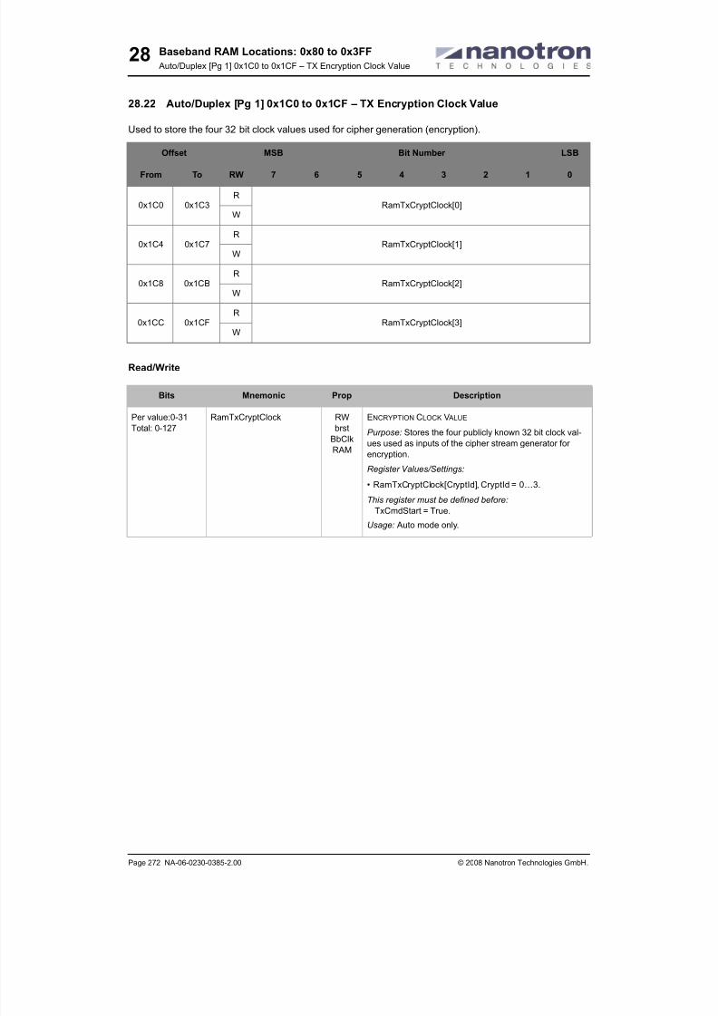
8/20/2019 nanoLOC NA5TR1 UserGuide
http://slidepdf.com/reader/full/nanoloc-na5tr1-userguide 288/325
Baseband RAM Locations: 0x80 to 0x3FF
Auto/Duplex [Pg 1] 0x1C0 to 0x1CF – TX Encryption Clock Value
Page 272 NA-06-0230-0385-2.00 © 2008 Nanotron Technologies GmbH.
28
28.22 Auto/Duplex [Pg 1] 0x1C0 to 0x1CF – TX Encryption Clock Value
Used to store the four 32 bit clock values used for cipher generation (encryption).
Read/Write
Offset MSB Bit Number LSB
From To RW 7 6 5 4 3 2 1 0
0x1C0 0x1C3R
RamTxCryptClock[0]W
0x1C4 0x1C7R
RamTxCryptClock[1]W
0x1C8 0x1CBR
RamTxCryptClock[2]W
0x1CC 0x1CF
R
RamTxCryptClock[3]W
Bits Mnemonic Prop Description
Per value:0-31
Total: 0-127
RamTxCryptClock RW
brst
BbClk
RAM
ENCRYPTION CLOCK V ALUE
Purpose: Stores the four publicly known 32 bit clock val-
ues used as inputs of the cipher stream generator for
encryption.
Register Values/Settings:
• RamTxCryptClock[CryptId], CryptId = 0…3.
This register must be defined before:
TxCmdStart = True.
Usage: Auto mode only.

8/20/2019 nanoLOC NA5TR1 UserGuide
http://slidepdf.com/reader/full/nanoloc-na5tr1-userguide 289/325
Baseband RAM Locations: 0x80 to 0x3FF
Auto/Duplex [Pg 1] 0x1D0 to 0x1DF – Reserved
© 2008 Nanotron Technologies GmbH. NA-06-0230-0385-2.00 Page 273
28
28.23 Auto/Duplex [Pg 1] 0x1D0 to 0x1DF – Reserved
These RAM locations are reserved.
Offset MSB Bit Number LSB
From To RW 7 6 5 4 3 2 1 0
0x1D0 0x1DFR
ReservedW

8/20/2019 nanoLOC NA5TR1 UserGuide
http://slidepdf.com/reader/full/nanoloc-na5tr1-userguide 290/325
Baseband RAM Locations: 0x80 to 0x3FF
Auto/Duplex [Pg 1] 0x1E0 to 0x1EF – RX Decryption Clock Value
Page 274 NA-06-0230-0385-2.00 © 2008 Nanotron Technologies GmbH.
28
28.24 Auto/Duplex [Pg 1] 0x1E0 to 0x1EF – RX Decryption Clock Value
Used to store the four 32 bit clock values used as input for cipher generation (decryption).
Read/Write
Offset MSB Bit Number LSB
From To RW 7 6 5 4 3 2 1 0
0x1E0 0x1E3R
RamRxCryptClock[1]W
0x1E4 0x1E7R
RamRxCryptClock[1]W
0x1E8 0x1EBR
RamRxCryptClock[2]W
0x1EC 0x1EF
R
RamRxCryptClock[3]W
Bits Mnemonic Prop Description
Per value:0-31
Total:0-127
RamRxCryptClock RW
brst
BbClk
RAM
RECEIVE DECRYPTION CLOCK
Purpose: Stores the four publicly known 32 bit clock val-
ues used as inputs of the cipher stream generator for
decryption.
Register Values/Settings:
• RxCryptClock[CryptId], CryptId = 0…3.
This register must be defined before:
RxCmdStart = True.

8/20/2019 nanoLOC NA5TR1 UserGuide
http://slidepdf.com/reader/full/nanoloc-na5tr1-userguide 291/325
Baseband RAM Locations: 0x80 to 0x3FF
Auto/Duplex [Pg 1] 0x1F0 to 0x1FF – Reserved
© 2008 Nanotron Technologies GmbH. NA-06-0230-0385-2.00 Page 275
28
28.25 Auto/Duplex [Pg 1] 0x1F0 to 0x1FF – Reserved
These RAM locations are reserved.
Offset MSB Bit Number LSB
From To RW 7 6 5 4 3 2 1 0
0x1F0 0x1FFR
ReservedW

8/20/2019 nanoLOC NA5TR1 UserGuide
http://slidepdf.com/reader/full/nanoloc-na5tr1-userguide 292/325
Baseband RAM Locations: 0x80 to 0x3FF
Auto/Duplex [Pg 2] 0x200 to 0x27F – Register (Mirrored)
Page 276 NA-06-0230-0385-2.00 © 2008 Nanotron Technologies GmbH.
28
28.26 Auto/Duplex [Pg 2] 0x200 to 0x27F – Register (Mirrored)
The nanoLOC chip register (0x00 to 0x7F) is mirrored to RAM locations 0x200 to 0x27F.
Offset MSB Bit Number LSB
From To RW 7 6 5 4 3 2 1 0
0x200 0x27FR
Mirrored Register (0x00 to 0x7F)W

8/20/2019 nanoLOC NA5TR1 UserGuide
http://slidepdf.com/reader/full/nanoloc-na5tr1-userguide 293/325

8/20/2019 nanoLOC NA5TR1 UserGuide
http://slidepdf.com/reader/full/nanoloc-na5tr1-userguide 294/325
Baseband RAM Locations: 0x80 to 0x3FF
Auto/Duplex [Pg 3] 0x300 to 0x37F – Register (Mirrored)
Page 278 NA-06-0230-0385-2.00 © 2008 Nanotron Technologies GmbH.
28
28.28 Auto/Duplex [Pg 3] 0x300 to 0x37F – Register (Mirrored)
The nanoLOC chip register (0x00 to 0x7F) is mirrored to RAM locations 0x300 to 0x37F.
Offset MSB Bit Number LSB
From To RW 7 6 5 4 3 2 1 0
0x200 0x27FR
Mirrored Register (0x00 to 0x7F)W

8/20/2019 nanoLOC NA5TR1 UserGuide
http://slidepdf.com/reader/full/nanoloc-na5tr1-userguide 295/325
Baseband RAM Locations: 0x80 to 0x3FF
Auto/Duplex [Pg 3] 0x380 to 0x3FF – TX Data Buffer
© 2008 Nanotron Technologies GmbH. NA-06-0230-0385-2.00 Page 279
28
28.29 Auto/Duplex [Pg 3] 0x380 to 0x3FF – TX Data Buffer
Used to store 128 bytes (1024 bits) of data in two buffers of 64 bytes each for a Data packet to be transmit-
ted.
Read/Write
Offset MSB Bit Number LSB
From To RW 7 6 5 4 3 2 1 0
0x380 0x3FFR
RamTxBuffer W
Bits Mnemonic Prop Description
0-1023 RamTxBuffer RW
brstBbClk
RAM
128 BYTE TX D ATA BUFFER
Purpose: Stores in two buffers of 64 bytes each the data to be
set in of a Data packet that is to be transmitted.

8/20/2019 nanoLOC NA5TR1 UserGuide
http://slidepdf.com/reader/full/nanoloc-na5tr1-userguide 296/325
Baseband RAM Locations: 0x80 to 0x3FF
Auto/Simplex [Pg 0] 0x80/0x0FF – Same as Auto/Duplex [Pg 0]
Page 280 NA-06-0230-0385-2.00 © 2008 Nanotron Technologies GmbH.
28
28.30 Auto/Simplex [Pg 0] 0x80/0x0FF – Same as Auto/Duplex [Pg 0]
Auto/Simplex Page 0 is identical to Auto/Duplex Page 0, which is replicated below.
Offset MSB Bit Number LSB
From To RW 7 6 5 4 3 2 1 0
Register SpaceR
Mirrored Register (0x00 to 0x7F)W
0x80 0x85R
RamStaAddr0W
0x86 0x87R
ReservedW
0x88 0x8DR
RamStaAddr1W
0x8E 0x8FR
ReservedW
0x90 0x95R
RamTxDstAddr W
0x96 0x97R
ReservedW
0x98 0x98R
RamTxLength
W
0x99 0x99
RTX Transparent Bits
for SW usageRamTxLength
W
0x9A 0xA7R
ReservedW
0xA8 0xADR
RamRxDstAddr W
0xAE 0xAFR
Reserved
W
0xB0 0xB5R
RamRxSrcAddr W
0xB6 0xB7R
ReservedW
0xB8 0xB8R
RamRxLengthW
0xB9 0xB9
RRX Transparent Bits
for SW usageRamRxLength
W

8/20/2019 nanoLOC NA5TR1 UserGuide
http://slidepdf.com/reader/full/nanoloc-na5tr1-userguide 297/325
Baseband RAM Locations: 0x80 to 0x3FF
Auto/Simplex [Pg 0] 0x80/0x0FF – Same as Auto/Duplex [Pg 0]
© 2008 Nanotron Technologies GmbH. NA-06-0230-0385-2.00 Page 281
28
0xBA 0xDF
R
ReservedW
0xE0 0xE5R
RamRtcTxW
0xE6 0xE7R
ReservedW
0xE8 0xEDR
RamRtcRxW
0xEE 0xEFR
Reserved
W
0xF0 0xFFR
RamRtcRegW
Offset MSB Bit Number LSB
From To RW 7 6 5 4 3 2 1 0

8/20/2019 nanoLOC NA5TR1 UserGuide
http://slidepdf.com/reader/full/nanoloc-na5tr1-userguide 298/325
Baseband RAM Locations: 0x80 to 0x3FF
Auto/Simplex [Pg 1] 0x180/0xEFF – Same as Auto/Duplex [Pg 1]
Page 282 NA-06-0230-0385-2.00 © 2008 Nanotron Technologies GmbH.
28
28.31 Auto/Simplex [Pg 1] 0x180/0xEFF – Same as Auto/Duplex [Pg 1]
Auto/Simplex Page 1 is identical to Auto/Duplex Page 1, which is replicated below.
Offset MSB Bit Number LSB
From To RW 7 6 5 4 3 2 1 0
Register SpaceR
Mirrored Register (0x00 to 0x7F)W
0x180 0x18FR
RamTxRxCryptKeyW
0x190 0x1BFR
ReservedW
0x1C0 0x1CF
R
RamTxCryptClockW
0x1D0 0x1DFR
ReservedW
0x1E0 0x1EFR
RamRxCryptClockW
0x1F0 0x1FFR
ReservedW

8/20/2019 nanoLOC NA5TR1 UserGuide
http://slidepdf.com/reader/full/nanoloc-na5tr1-userguide 299/325
Baseband RAM Locations: 0x80 to 0x3FF
Auto/Simplex [Pg 2/3] 0x280 to 0x3FF – TX/RX Data Buffer
© 2008 Nanotron Technologies GmbH. NA-06-0230-0385-2.00 Page 283
28
28.32 Auto/Simplex [Pg 2/3] 0x280 to 0x3FF – TX/RX Data Buffer
Used for storing sequentially transmit and receive data, where the entire 256 bytes are divided into two 128
byte (2048 bit) buffers as a combined receive/transmit buffer. As this is Simplex mode, the transmit and
receive buffer operations are dependent on each other, in that the receive operation must be completed
before the transmit operation can be initiated. Consequently, the buffer for the RX data and for the TX data
is double the size, in this case, 256 bytes.
Read/Write
Offset MSB Bit Number LSB
From To RW 7 6 5 4 3 2 1 0
Register SpaceR
Mirrored Register (0x00 to 0x7F)W
0x280 0x2FFR
RamTxRxBuffer W
Register SpaceR
Mirrored Register (0x00 to 0x7F)W
0x380 0x3FFR
RamTxRxBuffer W
Bits Mnemonic Prop Description
0-2047 RamTxRxBuffer RW
brst
BbClkRAM
256 BYTE SHARED TRANSMIT/RECEIVE D ATA BUFFER
Purpose: Stores both received data and data for transmission(sequentially) in a combined RX/TX buffer.

8/20/2019 nanoLOC NA5TR1 UserGuide
http://slidepdf.com/reader/full/nanoloc-na5tr1-userguide 300/325
Baseband RAM Locations: 0x80 to 0x3FF
Transparent/Duplex Page [Pg 0/1] 0x080 to 0x1FF – RX Data Buffer
Page 284 NA-06-0230-0385-2.00 © 2008 Nanotron Technologies GmbH.
28
28.33 Transparent/Duplex Page [Pg 0/1] 0x080 to 0x1FF – RX Data Buffer
The RX data buffer, which is used for storing the MACFrame from a received packet, is a 256 byte buffer
divided into two 128 byte buffers.
As this is Transparent mode, software is responsible fro maintaining MACFrame variables. As this is Duplexmode, received data can saved to this buffer while data to be transmitted can be simultaneously written to
the TX data buffer RamTxTransBuffer.
Read/Write
Offset MSB Bit Number LSB
From To RW 7 6 5 4 3 2 1 0
Register SpaceR
Mirrored Register (0x00 to 0x7F)W
0x080 0x0FFR
RamRxTransBuffer W
Register SpaceR
Mirrored Register (0x00 to 0x7F)W
0x180 0x1FFR
RamRxTransBuffer W
Bits Mnemonic Prop Description
0-2047 RamRxTransBuffer RW
brstBbClk
RAM
256 BYTE RECEIVE BUFFER
Purpose: Stores the received data in two 128 byte buffers.

8/20/2019 nanoLOC NA5TR1 UserGuide
http://slidepdf.com/reader/full/nanoloc-na5tr1-userguide 301/325
Baseband RAM Locations: 0x80 to 0x3FF
Transparent/Duplex Page [Pg 2/3] 0x280 to 0x3FF – TX Data Buffer
© 2008 Nanotron Technologies GmbH. NA-06-0230-0385-2.00 Page 285
28
28.34 Transparent/Duplex Page [Pg 2/3] 0x280 to 0x3FF – TX Data Buffer
The TX Data Buffer, which is used for storing completed MACFrames from software for transmission, is a
256 byte buffer divided into two 128 byte buffers.
As this is Transparent mode, software is responsible fro maintaining MACFrame variables. As this is Duplexmode, data for transmission can written to this buffer while received data can be simultaneously saved to
the RX Data Buffer RamRxTransBuffer.
Read/Write
Offset MSB Bit Number LSB
From To RW 7 6 5 4 3 2 1 0
Register SpaceR
Mirrored Register (0x00 to 0x7F)W
0x280 0x2FFR
RamTxTransBuffer W
Register SpaceR
Mirrored Register (0x00 to 0x7F)W
0x380 0x3FFR
RamTxTransBuffer W
Bits Mnemonic Prop Description
0-2047 RamTxTransBuffer RW
brstBbClk
RAM
256 BYTE TRANSMIT BUFFER
Purpose: Stores the data to be transmitted in two 128 byte
buffers.

8/20/2019 nanoLOC NA5TR1 UserGuide
http://slidepdf.com/reader/full/nanoloc-na5tr1-userguide 302/325
Baseband RAM Locations: 0x80 to 0x3FF
Transparent/Simplex [Pg 0/1/2/3] 0x080/0x3FF – RX/TX Data Buffer
Page 286 NA-06-0230-0385-2.00 © 2008 Nanotron Technologies GmbH.
28
28.35 Transparent/Simplex [Pg 0/1/2/3] 0x080/0x3FF – RX/TX Data Buffer
The RX/TX data buffer is a single 512 byte buffer divided into four 128 byte buffers. It is used for storing
sequentially MACFrames from a received packet to be read from software, or MACFrames provided by soft-
ware to be transmitted in packets over the air.
As this is Transparent mode, software is responsible fro maintaining MACFrame variables. As this is Sim-
plex mode, the transmit and receive buffer operations are dependent of each other so that a receive opera-
tion must be completed first before a transmit operation can be initiated. Consequently, the buffer size
available for the RX or TX data is the complete baseband RAM memory space of 512 bytes.
Read/Write
Offset MSB Bit Number LSB
From To RW 7 6 5 4 3 2 1 0
Register SpaceR
Register (0x00 to 0x7F)W
0x080 0x0FFR
RamTxRxTransBuffer W
Register SpaceR
Mirrored Register (0x00 to 0x7F)W
0x180 0x1FFR
RamTxRxTransBuffer W
Register SpaceR
Mirrored Register (0x00 to 0x7F)W
0x280 0x2FF
R
RamTxRxTransBuffer W
Register SpaceR
Mirrored Register (0x00 to 0x7F)W
0x380 0x3FFR
RamTxRxTransBuffer W
Bits Mnemonic Prop Description
0-4095 RamTxRxTransBuffer RW
brst
BbClk
RAM
512 BYTE SHARED TRANSMIT/RECEIVE BUFFER
Purpose: Sequentially stores the received data or the data to
be transmitted in a combined 512 byte RX/TX buffer.

8/20/2019 nanoLOC NA5TR1 UserGuide
http://slidepdf.com/reader/full/nanoloc-na5tr1-userguide 303/325
A p p e n d i c e s

8/20/2019 nanoLOC NA5TR1 UserGuide
http://slidepdf.com/reader/full/nanoloc-na5tr1-userguide 304/325

8/20/2019 nanoLOC NA5TR1 UserGuide
http://slidepdf.com/reader/full/nanoloc-na5tr1-userguide 305/325
Attributes and Constants
nanoLOC TRX Transceiver (NA5TR1) User Guide
© 2008 Nanotron Technologies GmbH. NA-06-0230-0385-2.00 Page 289
A1
A1 Attributes and Constants
The following table lists the attributes and constants referred to in this document.
The following three figures illustrate the attributes and constants defined in this appendix:
Table 3: Attributes and Constants
Symbol Value Description
MacAckTimeMax MacSifsTime + 2 • MacAirDelTimeMax = 24 µsMaximum time out for receiving an Ack
packet.
MacAirDelTimeMax < 8 µs (< 2.4 km)MAC Air Delay Time Maximum (maximum
air interface delay).a
a. See f igure 22. Carrier sense interframe space time (CIFS) on page 290 and figure 23. Air interface delay on page 290 .
MacArqCntMax 0 to 14Maximum allowed number of retransmis-
sion attempts for Data packets.
MacBrdcastLengthMax 8192 bytesMaximum allowed length of the data field of
Brdcast packets in bytes.
MacCifsTime MacSifsTime + 2 • MacAirDelTimeMax = 24 µsCarrier Sense Interframe Space Time
(CIFS).
b
b. See f igure 22. Carrier sense interframe space time (CIFS) on page 290 .
MacClr2STimeMax MacSifsTime + 2 • MacAirDelTimeMax = 24 µsMaximum time out for receiving a Clr2S
packet.
MacDataLengthMax 8192 bytesMaximum allowed length of the data field of
Data packets in bytes.
MacPreambleSymbols 30 Number of preamble symbols.
MacSifsTime 8 µs
Switching Interframe Space Time (SIFS) –
(switching time from reception to transmis-
sion of symbols (air interface)).c
c. See figure 21. Switching interframe space time (SIFS) on page 290 and figure 22. Carrier sense interframe space time (CIFS)on page 290 .
MacSlotTime MacSifsTime + 2 • MacAirDelTimeMax = 24 µs Duration of an back-off slot.d
d. See f igure 23. Air interface delay on page 290 .
MacSlotUncertainty MacAirDelTimeMax = 8 µsUncertainty of back-off slot alignment due
to air propagation delay.e
e. See f igure 23. Air interface delay on page 290 .
MacTailSymbols 4 Number of tail symbols.

8/20/2019 nanoLOC NA5TR1 UserGuide
http://slidepdf.com/reader/full/nanoloc-na5tr1-userguide 306/325
Attributes and Constants
nanoLOC TRX Transceiver (NA5TR1) User Guide
Page 290 NA-06-0230-0385-2.00 © 2008 Nanotron Technologies GmbH.
A1
Figure 21: Switching interframe space time (SIFS)
Figure 22: Carrier sense interframe space time (CIFS)
Figure 23: Air interface delay
Txair interface
Rxair interface
TxMode
Rx symbols
Tx symbols
TxDelay3RxDelay1 Internal switching time2
MacSifsTime
1. Propagation delay from air interface to digital symbol decoding and to carrier sensing mechanism.2. Switching time from symbol decoding to transmit initiation.
3. Propagation delay from transmit initiation to air interface (includes transmitter ramp up).
Tx STA1
Rx STA2
Tx STA2
Rx STA1
MacAirDelTimeMax
MacSifsTime
MacCifsTime
MacAirDelTimeMax
Tx STA1
Rx STAx
Rx symbols/RSSI
Internal switching time
RxDelay
TxDelay
MacAirDelTimeMax
MacSlotTime
-MacSlotUncertainty +MacSlotUncertainty
Backoffslots

8/20/2019 nanoLOC NA5TR1 UserGuide
http://slidepdf.com/reader/full/nanoloc-na5tr1-userguide 307/325

8/20/2019 nanoLOC NA5TR1 UserGuide
http://slidepdf.com/reader/full/nanoloc-na5tr1-userguide 308/325
Chip Registers Default Settings
nanoLOC TRX Transceiver (NA5TR1) User Guide
Page 292 NA-06-0230-0385-2.00 © 2008 Nanotron Technologies GmbH.
A2
2 WO UsePullup4Spissn 0x0No pull-up resistor connected to the SPISsn
pad
3 WO UsePulldown4Spissn 0x0No pull-down resistor connected to the
SPISsn pad
4 WO UsePullup4Spirxd 0x0No pull-up resistor connected to the SPIRxD
pad
5 WO UsePulldown4Spirxd 0x0No pull-down resistor connected to the
SPIRxD pad
6 WO UsePullup4Spitxd 0x0No pull-up resistor connected to the SPITxD
pad
7 WO UsePulldown4Spitxd 0x0No pull-down resistor connected to the
SPITxD pad
0x0A 0 WO UsePullup4Por 0x0 No pull-up resistor connected to POR Pad
1 WO UsePulldown4Por 0x0No pull-down resistor connected to POR
Pad
2 WO UsePullup4Pamp 0x0 No pull-up resistor connected to TxRx Pad
3 WO UsePulldown4Pamp 0x0 No pull-down resistor connected TxRx Pad
4 WO UsePullup4Ucirq 0x0 No pull-up resistor connected to µcIRQ Pad
5 WO UsePulldown4Ucirq 0x0No pull-down resistor connected to µcIRQ
Pad
6 WO UsePullup4Ucrst 0x0 No pull-up resistor connected to µcRST Pad
7 WO UsePulldown4Ucrst 0x0No pull-down resistor connected to µcRST
Pad
0xB 0 WO WritePulls4Spi 0x0 Write Pull-up and Pull-down settings to thefour SPI Pads
1 WO WritePulls4Pads 0x0Write Pull-up and Pull-down settings to the
four additional Pads
0x0C 0-3 RW TestModes 0x0Default setting - Switches off transceiver test
mode - INTERNAL
0x0D 0 WO RfTestSelect 0x0 NA_RfTestSelTxDacCmd_C - INTERNAL
0x0E 0-1 RW RamIndex 0x0 Baseband RAM block 0
4-5 RW DeviceSelect 0x0 Select baseband RAM
0x0F 0 RW TxIrqEnable 0x0 TX interrupt does not drive the interrupt line
1 RW RxIrqEnable 0x0 RX interrupt does not drive the interrupt line
2 RW BbTimerIrqEnable 0x0BbTimer interrupt does not drive the inter-
rupt line
3 RW LoIrqEnable 0x0 LO interrupt does not drive the interrupt line
4 RO TxIrqStatus 0x0 Event did not trigger
5 RO RxIrqStatus 0x0 Event did not trigger
6 RO BbTimerIrqStatus 0x0 Event did not trigger
7 RO LoIrqStatus 0x0 Event did not trigger
0x10 0-5 RO TxIntsRawStat Transmitter Interrupt Raw Status
0-5 WO TxIntsReset Transmitter Interrupt Reset
0-1 TxBufferRdy 0x0 Transmit Buffer Ready
2 TxEnd 0x0 Transmit End
Table 4: Chip registers default settings (Continued)
Register Bit RW Field Default Description

8/20/2019 nanoLOC NA5TR1 UserGuide
http://slidepdf.com/reader/full/nanoloc-na5tr1-userguide 309/325
Chip Registers Default Settings
nanoLOC TRX Transceiver (NA5TR1) User Guide
© 2008 Nanotron Technologies GmbH. NA-06-0230-0385-2.00 Page 293
A2
3 TxUnderrun 0x0 Transmit Buffer Underrun
4 TxTimeSlotTOut 0x0 Transmit Time Slot Time-out
5 TxTimeSlotEnd 0x0 Transmit Time Slot End
0x11 0-6 RO RxIntsRawStat 0x0 Receiver Interrupt Raw Status
0-6 WO RxIntsReset Reset Receiver Interrupt
0-1 RxBufferRdy 0x0 Receive Buffer Ready
2 RxEnd 0x0 End of Packet Reception
3 RxHeaderEnd 0x0 End of Correct Header Reception
4 RxOverflow 0x0 Receive Buffer Overflow
5 RxTimeSlotTOut 0x0 Receive Time Slot Time-out
6 RxTimeSlotEnd 0x0 Receive Time Slot End
0x12 1 RO LoIntsRawStat 0x0 Local Oscillator Interrupt Raw Status
1 WO LoIntsReset Reset Local Oscillator interrupt
7 WO ClearBasebandTimerInt 0x0 Baseband timer interrupt reset
1 LoTuningReady 0x0 Local Oscillator Tuning Ready
0x13 0-5 WO TxIntsEn 0x0 Enable Transmitter Interrupt
0-1 TxBufferRdy 0x0 Transmit Buffer Ready
2 TxEnd 0x0 Transmit End
3 TxUnderrun 0x0 Transmit Buffer Underrun
4 TxTimeSlotTOut 0x0 Transmit Time Slot Time-out
5 TxTimeSlotEnd 0x0 Transmit Time Slot End
0x14 0-6 WO RxIntsEn 0x0 Enable Receiver Interrupt
1-0 RxBufferRdy 0x0 Receive Buffer Ready
2 RxEnd 0x0 End of Packet Reception
3 RxHeaderEnd 0x0 End of Correct Header Reception
4 RxOverflow 0x0 Receive Buffer Overflow
5 RxTimeSlotTOut 0x0 Receive Time Slot Time-out
6 RxTimeSlotEnd 0x0 Receive Time Slot End
0x15 1 WO LoIntsEn Enable Local Oscillator interrupt
1 LoTuningReady 0x0 Local Oscillator Tuning Ready
0x16-0x18 0-21 RW LoRxCapsValue 0x200040 Read or Write the Caps Value for RX
0x19-0x1B 0-21 RW LoTxCapsValue 0x200040 Read or Write the Caps Value for TX
0x1C 0 WO LoEnableFastTuning 0x0 Disable Accelerated LO Caps Tuning
1-3 WO LoFastTuningLevel 0x0 Lowest LO Caps Tuning Level
4 WO LoEnableLsbNeg 0x0No Higher Precision Accelerated LO Caps
Tuning
7 WO UseLoRxCaps 0x0 Use TX caps for LO caps tuning
0x1D-
0x1E0-16 RW LoTargetValue target value for center frequency
0x1F 0-7 WO AgcThresHold1 0x3 lower level of the integration value is 3
Table 4: Chip registers default settings (Continued)
Register Bit RW Field Default Description

8/20/2019 nanoLOC NA5TR1 UserGuide
http://slidepdf.com/reader/full/nanoloc-na5tr1-userguide 310/325
Chip Registers Default Settings
nanoLOC TRX Transceiver (NA5TR1) User Guide
Page 294 NA-06-0230-0385-2.00 © 2008 Nanotron Technologies GmbH.
A2
0x20 0-7 WO AgcThresHold2 0x6Upper level of the integration value:
AgcThreshHold1 + 6
0x21 0-6 WO HoldAgcInBitSync 0x18“In bit synchronization state, gain is not
changed after 24 pulses are received”
7 WO HoldAgcInFrameSync 0x1Hold AGC when the receiver reaches frame
synchronization state
0x22 0-5 AgcDeadTime 0xC12 cycles before the next integration phase -
INTERNAL
6-7 WO AgcNregLength 0x0 Gain Length N = 5
0x23-0x24 0-12 WO AgcIntTime 0x200 512 cycles for AGC integration
0x25 0-5 WO AgcValue 0x3F AGC value used for RX amplifiers is 64
6 WO AgcDefaultEn 0x0 Ignore default Agc Value
7 WO AgcHold 0x0 RF AGC is active
0x26 0-5 RO AgcGain 0x0 Read GAIN for Current Packet
0-5 WO AgcRssiThres 0x1E
“When gain is below 31, media is interpreted
as busy when the upper bit of the
TxPhCarrSenseMode field is set to 1”
7 WO AgcEnable 0x0 Disables AGC - INTERNAL
0x27 0-5 RO FctPeriod 0x0Counts the amount of 16MHz clock periods
during a FCT clock cycle
0-3 WO ChirpFilterCaps 0x06Switches the capacitors of the chirp filter to
adjust the FCT clock to 400kHz
4 WO FctClockEn 0x0 RF TX FCT clock disabled
5 WO StartFctMeasure 0x0 RF TX FCT Measurement not active
7 WO EnableTx 0x0 Disable manual starting of TX
0x28-0x29 0-15 WO BasebandTimerStartValue 0x0 Start value of the timer
0x2A-
0x2B0-12 RO ToaOffsetMeanAck 0x0
ToA Offset for Received Ack Packet -
INTERNAL
15 RO ToaOffsetMeanAckValid 0x0Reports that enough pulses were received
at end of Ack packet - INTERNAL
0x2C-
0X2D0-15 RO TxRespTime 0x0 TX Response Round Trip Time - INTERNAL
0x2E 0-2 RO PhaseOffsetAck 0x0PhaseOffset for Received Ack Packet -
INTERNAL
4-6 RO PhaseOffsetData 0x0PhaseOffset for Received Data Packet -
INTERNAL
0x2F-0x30 0-12 RO ToaOffsetMeanData 0x0ToA Offset for Received Data Packet -
INTERNAL
15 ToaOffsetMeanDataValid 0x0
Reports if enough pulses were received to
provide a valid time measurement - INTER-
NAL
0x2A-0x31 0-63 WO SyncWord
0x0xAB69
CA9492D
52CAB
Inital Transceiver Syncword is
0x0xAB69CA9492D52CAB
0x31 0-3 RO RxPacketType Receive Packet Type
4-5 RO RxAddrMatch 0x0Received destination address does notmatch the station address set in
RamStaAddr0/1
Table 4: Chip registers default settings (Continued)
Register Bit RW Field Default Description

8/20/2019 nanoLOC NA5TR1 UserGuide
http://slidepdf.com/reader/full/nanoloc-na5tr1-userguide 311/325
Chip Registers Default Settings
nanoLOC TRX Transceiver (NA5TR1) User Guide
© 2008 Nanotron Technologies GmbH. NA-06-0230-0385-2.00 Page 295
A2
6 RO RxCrc1Stat 0x0 CRC1 check has failed
7 RO RxCrc2Stat 0x0 CRC2 check has failed
0x32 0-3 RO RxCorrBitErr 0x00 bit errors occurred during Syncword corre-
lation
4-7 WO RxCorrErrThres 0x3 Maximum 3 syncword errors allowed
0x33-0x34 0-15 WO TxTimeSlotStart 0x0Defines the beginning of the time slot for a
transmission
0x35-0x36 0-15 WO TxTimeSlotEndDefines the end of the time slot for a trans-
mission
0x33 0 RO RxAddrSegEsMatch 0x0 End station address does not match
1 RO RxAddrSegIsMatch 0x0Intermediate Station address does not
match
4 RO RxCryptEn 0x0 Disable reading of the CryptEn Bit value
5-6 RO RxCryptId 0x0Reads the value of the two bit Encryption ID
field
7 RO RxCryptSeqN 0x0Reads the value of the one bit sequential
numbering scheme for encryption
0x34-0x35 0-14 RO RxFec1BitErr 0x0Reports the number of correctable single bit
errors that have occurred in a receive packet
0x36 RO Reserved
0x37 0 WO TxTimeSlotControl 0x0Disable TX Time slot control - packets are
transmitted independent of the time slot
1 WO RxTimeSlotControl 0x0
Activates the receiver independent of the
defined time slot through the RxCmd com-mand
0x38-0x39 0-15 RO RxPacketSlot 0x0 Reports time at the packet header end event
0-15 WO RxTimeSlotStart 0x0Defines the beginning of the time slot for a
reception
0x3A-
0x3B0-15 WO RxTimeSlotEnd 0x0
Defines the end of the time slot for a recep-
tion
0x3C 0-3 RO TxArqCnt 0x0reports the required number of retransmis-
sions
4-7 WO TxArqMax 0xESets the maximal value for packet retrans-
missions
0x3D 0-1 WO CsqDitherValue 0x0 no Chirp Sequencer dither
2 WO CsqUsePhaseShift 0x0 Disable Phase Shift
3 WO CsqUse4Phases 0x0 Disables four phases
4 WO ScqAsyMode 0x0 Disable Asymmetric Mode
5 WO CsqMemAddrInit 0x0Disables initialize of chirp sequencer mem-
ory address
6 WO CsqUseRam 0x0 Disable Chirp Sequencer RAM
7 WO CsqTest 0x0Disables Test RF Transmit Chirp - INTER-
NAL
0x3E 0-5 WO CsqSetValue 0x0 Set Chirp Sequencer Value - INTERNAL
6 WO CsqSetIValue 0x0
Don’t set the I value in the Chirp Sequencer
with the value programmed in CsqSetValue
- INTERNAL
Table 4: Chip registers default settings (Continued)
Register Bit RW Field Default Description

8/20/2019 nanoLOC NA5TR1 UserGuide
http://slidepdf.com/reader/full/nanoloc-na5tr1-userguide 312/325
Chip Registers Default Settings
nanoLOC TRX Transceiver (NA5TR1) User Guide
Page 296 NA-06-0230-0385-2.00 © 2008 Nanotron Technologies GmbH.
A2
7 WO CsqSetQValue 0x0
Don’t set the Q value in the Chirp
Sequencer with the value programmed in
CsqSetValue - INTERNAL
0x3F 0 WO D3IFixnMap 0x1 use FIX mode
1 WO D3lPomEn 0x0Disables the mean value calculation in the
Correlator
2-3 WO D3lPomLen 0x0The last 2 values should be used for calcu-
lating the mean value
7 WO D3IUpDownEx 0x0 Disables exchange of Up and Down Pulses
0x40 0-6 WO LeaveMapThresh1InBitsync 0x3switch back to Fix mode after 3 detected
pulses
7 WOUseMapThresh1InFramesyn
c0x0 use FIX with Threshold0
0x41 0 WO Go2MapThresh1InBitsync 0x7
Switch from FIX mode using correlator
threshold 0 to either MAP mode or FIX
mode using correlator threshold 1 after 7
detected pulses in bit synchronization state.
1 WO D3lFixThres1MapEn 0x0Disable MAP mode or FIX mode using corr-
elator threshold1 INTERNAL
0x42 0 WO EnableLO 0x0 Disable RF local Oscillator
1 WO EnableLOdiv10 0x0 Disable LO frequency divide by 10 function
2 WO EnableCsqClock 0x0 Disable Chirp Sequencer Clock
3 WO InvertRxClock 0x0Disable changing sampling Edge for
receiver
4 WO EnableExtPA Enable External Power Amplifier Output
5 WO EnableIntPA 0x0 Disable Power Internal Amplifier INTERNAL
6 WO EnableRxClock 0x0 Disable the receiver clock INTERNAL
7 WO EnableRX 0x0 Disable RF Receiver INTERNAL
0x43 0-2 WO LnaFreqAdjust 0x3 Adjust RF Receiver LNA Frequency
4-6 WO TxPaBias 0x0 Adjust RF Transmitter Power Amplifier Bias
0x44 0-5 WO TxOutputPower0 0x3F Set RF TX Output Power0 to 63
0x45 0-5 WO TxOutputPower1 0x3F Set RF TX Output Power1 to 63
0x46 0-4 WO RfRxCompValueI 0xF Quantization Threshold for I
0x47 0 WO RfRxCompValueQ 0xF Quantization Threshold for Q
0x48 0-2 WO SymbolDur 0x3 Set symbol duration to 4000ns
4-6 WO SymbolRate 0x7 Set Symbol Rate to 250k Symbols
7 WO ModulationSystem 0x0 Selects the 2-ary modulation system
0x49 0-1 WO Crc2Type 0x0 Selects NA_Crc2type1_VC_C
2 WO UseFec 0x0 Disables FEC
3 WO TxRxCryptCrc2Mode 0x0Enables
NA_TxRxCryptCrc2ModeUncrypted_BC_C
4-7 WO TxRxCryptClkMode Set Encryption/Decryption Clock Mode
0x4A 0 RW SwapBbBuffers 0x0Data in buffers belong to their intended
direction
1 WO TxRxBbBufferMode1 0x0 Sets Duplex Mode
Table 4: Chip registers default settings (Continued)
Register Bit RW Field Default Description

8/20/2019 nanoLOC NA5TR1 UserGuide
http://slidepdf.com/reader/full/nanoloc-na5tr1-userguide 313/325
Chip Registers Default Settings
nanoLOC TRX Transceiver (NA5TR1) User Guide
© 2008 Nanotron Technologies GmbH. NA-06-0230-0385-2.00 Page 297
A2
2 WO TxRxBbBufferMode0 0x0 Sets Auto Mode
4 WO FdmaEnable 0x1 Enables FDMA - 22 MHz bandwidth is used
7 WO TxRxMode 0x0
Sets Auto mode - MACFrame is built as a
nanoLOC MACFrame with header informa-
tion and data
0x4B-
0x4C0-2 WO ChirpMatrix0 0x0 Downchirp
4-6 WO ChirpMatrix1 0x1 Upchirp
8-10 WO ChirpMatrix2 0x3 Plus Folded Chirp
12-
14WO ChirpMatrix3 0x4 Off Chirp
0x4D 0-1 WO TxPreTrailMatrix0 0x0 Downchirp
2-3 WO TxPreTrailMatrix1 0x1 UpChirp
4 WO TxUnderrunIgnore 0x1 Enable Underrun Ignore
7 WO TxMacCifsDis 0x0 Enable waiting for CIFS
0x4E 0 WO TxVCarrSens 0x0 Virtual Carrier Sensing OFF
1-2 WO TxPhCarrSenseMode 0x0 Physical Carrier Sensing Mode off
3 WO TxVCarrSensAck 0x0Disable Ack Packets for Virtual Carrier
Sense
4 WO TxArq 0x1
Enable TX ARQ (Automatic Repeat
Request) Error Correction Scheme for Data
Packets
5 WO Tx3Way 0x0 Disable three-way handshake
6 WO TxBackOffAlg Back-Off Algorithm
7 WO TxFragPrio 0x0 Disable Fragmentation Prioritization
0x4F 0-7 WO TxBackOffSeed 0x0 Disable Back-Off Seed
0x50 0-3 WO TxCryptSeqReset 0x0 Disable TX Decryption Sequence Reset
4 WO TxCryptEn 0x0 Disable Encryption
5-6 WO TxCryptId 0x0 Secret Key Selection for Encryption
7 WO TxCryptSeqN 0x0 Encryption Sequence Number
0x51 0-6 WO TxScrambInit 0x7FInitializes the value for the scrambling unit
with 127
7 WO TxScrambEn 0x1 Enables scrambling in a transmitted MAC-Frame
0x52-0x53 0-12 WO TxTransBytes 0x0Number of Data Bytes in TX MACFrame in
Transparent Mode
0x54 0-3 WO TxPacketType 0x0 Packet Type For Transmission in Auto Mode
7 WO TxAddrSlct 0x0 Source Address for Transmission
0x55 0 WO TxCmdStop 0x0 Don’t stop transmission
1 WO TxCmdStart 0x0 Don’t start transmission
2-3 WO TxBufferCmd 0x0 Transmit Buffer Ready for Transmission
0x56 0 WO RxCmdStop 0x0 Don’t stop reception
1 WO RxCmdStart 0x0 Don’t start reception
2 WO RxBufferCmd 0x0 Read Receive Buffer
Table 4: Chip registers default settings (Continued)
Register Bit RW Field Default Description

8/20/2019 nanoLOC NA5TR1 UserGuide
http://slidepdf.com/reader/full/nanoloc-na5tr1-userguide 314/325
Chip Registers Default Settings
nanoLOC TRX Transceiver (NA5TR1) User Guide
Page 298 NA-06-0230-0385-2.00 © 2008 Nanotron Technologies GmbH.
A2
0x57 0-3 WO RxCryptSeqReset 0x0 RX Decryption Sequence Reset
0x58-0x59 0-12 WO RxTransBytes 0x0 Number of Data Bytes in Received MAC-Frame in Transparent Mode (0=8192bytes)
0x5A 0 WO RxTimeBCrc1Mode 0x1Enable Receive TimeB packets CRC1
check.
1 WO RxCrc2Mode 0x1
RxEnd is only triggered when CRC2 check
succeeds. When the check fails the receiver
remains active to receive the next packet.
When overflow occurs this will be ignored.
2-3 WO RxArqMode 0x2
The ARQ scheme is based on the CRC1
and CRC2. An Ack packet is sent in
response to a Data packet only if CRC1,
CRC2, and address matching succeeded.
4 WO RxAddrSegEsMode 0x0 Disables End Station Address Matching
5 WO RxAddrSegIsMode 0x0Disable Intermediate Station Address
Matching
6-7 WO RxAddrSegDevIdL 0x0 Segmented Address Format
0x5B 0 WO RxDataEn 0x1 Enable Data packets Reception
1 WO RxBrdcastEn 0x1 Enable Broadcast Packet Reception
2 WO RxTimeBEn 0xq Enable TimeB Packet Reception
3 WO RxAddrMode 0x1 Sets Address Matching Mode
4-7 WO RangingPulses 0x5Use 24 Up and Down Pulses for ranging
INTERNAL
0x5C 0-4 WO PulseDetDelay 0x5 Delay for Pulse Detection is 5
0x5D 0-2 WO GateAdjThreshold 0x7
sets the required number of consecutive
pulses outside of the gate center to 7 before
a readjustment of the gate takes place
4 WO DownPulseDetectDis 0x0 Enable Detection of Down Pulses
5 WO UpPulseDetectDis 0x0 Enable Detection of Up Pulses
0x5E 0-1 WO GateSizeUnsync 0x1Sets gate size = 5 slots for unsynchronized
state
2-3 WO GateSizeBitsync 0x1Sets gate size = 5 slots for bit synchronized
state
4-5 WO GateSizeFramesync 0x1Sets gate size = 5 slots for synchronized
state
6 WO GateAdjBitsyncEn 0x1Enables gate adjustment in bit synchroniza-
tion state
7 WO GateAdjFramesyncEn 0x1Enables gate adjustment in frame synchro-
nization state
0x5F 0-2 WO Go2BitsyncThreshold 0x2
Sets the required number of consecutive
chirp pulses detected in the unsynchronized
state to go to bit synchronization state to 2
4-6 WO LeaveBitsyncThreshold 0x6
Sets the required number of consecutive
lost pulses in bit synchronization state to
return to the unsynchronized state to 6
0x60 0-7 WO RtcTimeBTxAdj 0x0
Before transmitting, the Real Time Clock
control value must be adjusted to compen-
sate for transmitter delays
Table 4: Chip registers default settings (Continued)
Register Bit RW Field Default Description

8/20/2019 nanoLOC NA5TR1 UserGuide
http://slidepdf.com/reader/full/nanoloc-na5tr1-userguide 315/325
Chip Registers Default Settings
nanoLOC TRX Transceiver (NA5TR1) User Guide
© 2008 Nanotron Technologies GmbH. NA-06-0230-0385-2.00 Page 299
A2
0x61 0-7 WO RtcTimeBRxAdj 0x0 Adjusts the Real Time Clock value after
reception to compensate for receiver delays
0x62 0 WO RtcCmdWr 0x0Do not Set RamRtcReg Value in Real Time
Clock
1 WO RtcCmdRd 0x0 Don’t Set Real Time Clock Value in RtcReg
4 WO RtcTimeBAutoMode 0x0
The value of RamRtcTx is transmitted in the
RTC field of the TimeB packet, while the
RTC value in a received TimeB packet is
stored in RamRtcRx
7 WO RtcTimeBTestMode 0x0Disables Real Time Clock TimeB Test Mode
- INTERNAL
0x63 0-4 WO AgcAmplitude 0x0 Amplitude of 0 is selected for alternative
AGC
0x64 0-3 WO AgcRangeOffset 0x0 AGC is temporarily halted when: | MeanValue - Middle | > 0
7 WO UseAlternativeAgc 0x0 Disables Alternative AGC
0x65-0x7C Reserved 0x0
0x7D 0 RW TxRxDigTestMode 0x0 Transceiver Digital Test Mode - INTERNAL
1 RO DebugMacRxCmd 0x0 Debug Mac Command is idle - INTERNAL
2 RO DebugMacTxCmd 0x0 Debug Mac Command is idle - INTERNAL
0x7E 0-3 RO DebugMacFsm 0x0 Debug Mac Fsm is idle - INTERNAL
4-7 RO DebugMacTxRxCtrl 0x0Debug MAC Transmit Receive Control is
idle - INTERNAL
0x7F 0 RO DebugBitProcFsm 0x0 Debug Bit Process Fsm is idle - INTERNAL
1 RO DebugBitProcTx 0x1Debug Bit Processing Unit is idle - INTER-
NAL
2 RO DebugBitProcRx 0x0Debug Bit Processing Unit is idle - INTER-
NAL
3 RO DebugRxDetStatus 0x1Debug Receiver Detector Status unsynchro-
nized - INTERNAL
Table 4: Chip registers default settings (Continued)
Register Bit RW Field Default Description

8/20/2019 nanoLOC NA5TR1 UserGuide
http://slidepdf.com/reader/full/nanoloc-na5tr1-userguide 316/325
Chip Registers Default Settings
nanoLOC TRX Transceiver (NA5TR1) User Guide
Page 300 NA-06-0230-0385-2.00 © 2008 Nanotron Technologies GmbH.
A2
Intentionally Left Blank

8/20/2019 nanoLOC NA5TR1 UserGuide
http://slidepdf.com/reader/full/nanoloc-na5tr1-userguide 317/325
Index
nanoLOC TRX Transceiver (NA5TR1) User Guide
© 2008 Nanotron Technologies GmbH. NA-06-0230-0385-2.00 Page 301
Index
Symbols
µCIRQ . . . . . . . . . . . . . . . . . . . . . . . . . . . . . . . . . . . . . . . . . . . 12µCIRQ, configuring . . . . . . . . . . . . . . . . . . . . . . . . . . . . . . . . . 13
µCReset . . . . . . . . . . . . . . . . . . . . . . . . . . . . . . . . . . . . . . . . . 12µCVcc . . . . . . . . . . . . . . . . . . . . . . . . . . . . . . . . . . . . . . . . . . . 12
Numerics
128 bit secret key, used in encryption . . . . . . . . . . . . . . . . . . 77128 byte receive buffer . . . . . . . . . . . . . . . . . . . . . . . . . . . . . 277128 byte register block . . . . . . . . . . . . . . . . . . . . . . . . . . . . . . 42128 byte transmit buffer . . . . . . . . . . . . . . . . . . . . . . . . . . . . 27914 bit code word . . . . . . . . . . . . . . . . . . . . . . . . . . . . . . . . . . . 7722 MHz bandwidth
enabled using FdmaEnable . . . . . . . . . . . . . . . . . . . 97, 20622 MHz channels . . . . . . . . . . . . . . . . . . . . . . . . . . . . . . . . . . . 7256 byte receive buffer . . . . . . . . . . . . . . . . . . . . . . . . . 284, 285256 byte shared buffer . . . . . . . . . . . . . . . . . . . . . . . . . . . . . 28332 bit clock value
changed for each transmission . . . . . . . . . . . . . . . . . . . . 77used in encryption . . . . . . . . . . . . . . . . . . . . . . . . . . . . . . 77
32.786 kHz Clock . . . . . . . . . . . . . . . . . . . . . . . . . . . . . . . . . . 15
32.786 kHz clock . . . . . . . . . . . . . . . . . . . . . . . . . . . . . . . . . . 1548 bit addressand IEEE standards . . . . . . . . . . . . . . . . . . . . . . . . . . . 103format of . . . . . . . . . . . . . . . . . . . . . . . . . . . . . . . . . . . . 103I/G address bit in . . . . . . . . . . . . . . . . . . . . . . . . . . . . . . 103U/L address bit in . . . . . . . . . . . . . . . . . . . . . . . . . . . . . 104used in encryption . . . . . . . . . . . . . . . . . . . . . . . . . . . . . . 77
512 byte shared buffer . . . . . . . . . . . . . . . . . . . . . . . . . . . . . 28680 MHz bandwidth
default value of FdmaEnable . . . . . . . . . . . . . . . . . . 97, 206
A
Accessing a register address location . . . . . . . . . . . . . . . . . . 43 Ack packet
and CSMA/CA . . . . . . . . . . . . . . . . . . . . . . . . . . . . . . . . . 87and retransmissions . . . . . . . . . . . . . . . . . . . . . . . . . . . . 90fields . . . . . . . . . . . . . . . . . . . . . . . . . . . . . . . . . . . . . . . . 53max time-out for receiving . . . . . . . . . . . . . . . . . . . . . . . 289not for Brdcast packets . . . . . . . . . . . . . . . . . . . . . . . . . . 53
not for TimeB packets . . . . . . . . . . . . . . . . . . . . . . . . . . . 54not used in unconfirmed transmission . . . . . . . . . . . . . . 102protocol for transmitting illustrated . . . . . . . . . . . . . . . . 100reasons for a failed . . . . . . . . . . . . . . . . . . . . . . . . . . . . . 90transmitted with lower power level . . . . . . . . . . . . . . . . . 93when not received . . . . . . . . . . . . . . . . . . . . . . . . . . . . . . 99
addresslocally administered . . . . . . . . . . . . . . . . . . . . . . . . . . . . 104setting as group . . . . . . . . . . . . . . . . . . . . . . . . . . . . . . . 103setting as individual . . . . . . . . . . . . . . . . . . . . . . . . . . . . 103universally administered . . . . . . . . . . . . . . . . . . . . . . . . 104
address formatdescribed . . . . . . . . . . . . . . . . . . . . . . . . . . . . . . . . . . . . 103
Address1described . . . . . . . . . . . . . . . . . . . . . . . . . . . . . . . . . . . . . 51all bits in set to 1 in Brdcast packets . . . . . . . . . . . . . . . 104contains destination address . . . . . . . . . . . . . . . . . . . . . . 51contains RTC in TimeB packets . . . . . . . . . . . . . . . . . . . 51
in Ack packets . . . . . . . . . . . . . . . . . . . . . . . . . . . . . . . . . 53in Brdcast packets . . . . . . . . . . . . . . . . . . . . . . . . . . . . . . 54in Clr2S packets . . . . . . . . . . . . . . . . . . . . . . . . . . . . . . . 55in Data packets . . . . . . . . . . . . . . . . . . . . . . . . . . . . . . . . 52in Req2S packets . . . . . . . . . . . . . . . . . . . . . . . . . . . . . . 55in TimeB packets . . . . . . . . . . . . . . . . . . . . . . . . . . . . 54, 55
Address2described . . . . . . . . . . . . . . . . . . . . . . . . . . . . . . . . . . . . . 51contains source address . . . . . . . . . . . . . . . . . . . . . . . . . 51in Brdcast packets . . . . . . . . . . . . . . . . . . . . . . . . . . . . . . 54in Data packets . . . . . . . . . . . . . . . . . . . . . . . . . . . . . . . . 52in Req2S packets . . . . . . . . . . . . . . . . . . . . . . . . . . . . . . 55in TimeB packets . . . . . . . . . . . . . . . . . . . . . . . . . . . . . . . 54
addressesand promiscuous mode . . . . . . . . . . . . . . . . . . . . . . . . . 104broadcast . . . . . . . . . . . . . . . . . . . . . . . . . . . . . . . . . . . . 255destination . . . . . . . . . . . . . . . . . . . . . . . . . . . . . . . . . . . 259IEEE convention . . . . . . . . . . . . . . . . . . . . . . . . . . 251, 253multicast . . . . . . . . . . . . . . . . . . . . . . . . . . . . . . . . . . . . 255
source . . . . . . . . . . . . . . . . . . . . . . . . . . . . . . . . . . . . . . 261addressing
message types . . . . . . . . . . . . . . . . . . . . . . . . . . . . . . . 104 AGC
controls . . . . . . . . . . . . . . . . . . . . . . . . . . . . . . . . . . . . . 166register settings . . . . . . . . . . . . . . . . . . . . . . . . . . . . . . 166
AGC calibration . . . . . . . . . . . . . . . . . . . . . . . . . . . . . . . . . . . 49 AGC hold
bit synchronization control . . . . . . . . . . . . . . . . . . . . . . 162frame synchronization control . . . . . . . . . . . . . . . . . . . 162
AgcAmplitude . . . . . . . . . . . . . . . . . . . . . . . . . . . . . . . . . . . 239 AgcIntTime . . . . . . . . . . . . . . . . . . . . . . . . . . . . . . . . . . . . . 164 AgcNregLength . . . . . . . . . . . . . . . . . . . . . . . . . . . . . . . . . . 163 AgcRangeOffset . . . . . . . . . . . . . . . . . . . . . . . . . . . . . . . . . 240 AgcRssiThres . . . . . . . . . . . . . . . . . . . . . . . . . . . . . . . . . . . 166 AgcThresHold1 . . . . . . . . . . . . . . . . . . . . . . . . . . . . . . . . . . 160 AgcThresHold2 . . . . . . . . . . . . . . . . . . . . . . . . . . . . . . . . . . 161 AgcValue . . . . . . . . . . . . . . . . . . . . . . . . . . . . . . . . . . . . . . . 165air interface . . . . . . . . . . . . . . . . . . . . . . . . . . . . . . . . . . . . . . 93all-stations broadcast
set by I/G address bit . . . . . . . . . . . . . . . . . . . . . . . . . . 103analog part, described . . . . . . . . . . . . . . . . . . . . . . . . . . . . . . . 9analog pin µCVcc described . . . . . . . . . . . . . . . . . . . . . . . . . 11architecture, of nanoLOC . . . . . . . . . . . . . . . . . . . . . . . . . . . . 9
ARQapplied only to Data packets . . . . . . . . . . . . . . . . . . . . 101
transmit count . . . . . . . . . . . . . . . . . . . . . . . . . . . . . . . . 188transmit maximum . . . . . . . . . . . . . . . . . . . . . . . . . . . . 188used to correct received data packets . . . . . . . . . . . . . . 99
Auto/Duplex . . . . . . . . . . . . . . . . . . . . . . . . . . . . . . . . . . . . . . 62 Auto/Simplex . . . . . . . . . . . . . . . . . . . . . . . . . . . . . . . . . . . . . 63automatic repeat request. See ARQ
B
backoff counter decremented until media busy . . . . . . . . . . . . . . . . . . . . 90frozen until media detected idle . . . . . . . . . . . . . . . . . . . 90initialization of . . . . . . . . . . . . . . . . . . . . . . . . . . . . . . . . . 90
backoff procedureillustrated . . . . . . . . . . . . . . . . . . . . . . . . . . . . . . . . . . . . 89
back-off slot . . . . . . . . . . . . . . . . . . . . . . . . . . . . . . . . . . . . . 289back-off slot alignment . . . . . . . . . . . . . . . . . . . . . . . . . . . . . 289backoff time
described . . . . . . . . . . . . . . . . . . . . . . . . . . . . . . . . . . . . 89designed to avoid collisions . . . . . . . . . . . . . . . . . . . . . . 87
backoff time slot. See BTSbandwidth
reserving with higher power level . . . . . . . . . . . . . . . . . . 93reserving with Req2S packet . . . . . . . . . . . . . . . . . . 49, 54wasting with collisions . . . . . . . . . . . . . . . . . . . . . . . . . . 91
Basebandaddress format . . . . . . . . . . . . . . . . . . . . . . . . . . . . . . . 103bit processing . . . . . . . . . . . . . . . . . . . . . . . . . . . . . . . . . 75data transmission control . . . . . . . . . . . . . . . . . . . . . . . . 99link control management . . . . . . . . . . . . . . . . . . . . . . . . 58logical channels . . . . . . . . . . . . . . . . . . . . . . . . . . . . . . . 57media access control . . . . . . . . . . . . . . . . . . . . . . . . . . . 87packets and frames . . . . . . . . . . . . . . . . . . . . . . . . . . . . 49resetting . . . . . . . . . . . . . . . . . . . . . . . . . . . . . . . . . . . . 129
Baseband clockdescribed . . . . . . . . . . . . . . . . . . . . . . . . . . . . . . . . . . . . 15enabling . . . . . . . . . . . . . . . . . . . . . . . . . . . . . . . . . . . . . 19stopping . . . . . . . . . . . . . . . . . . . . . . . . . . . . . . . . . . . . . 19
Baseband clock stopping distribution . . . . . . . . . . . . . . . . . . 20baseband timer event status of . . . . . . . . . . . . . . . . . . . . . . . . . . . . . . . 141IRQ enabling . . . . . . . . . . . . . . . . . . . . . . . . . . . . . 14, 140start values of . . . . . . . . . . . . . . . . . . . . . . . . . . . . . . . . 169
BasebandTimerStartValue . . . . . . . . . . . . . . . . . . . . . . . . . 169battery voltage comparator
enabling . . . . . . . . . . . . . . . . . . . . . . . . . . . . . . . . . . . . 121level for . . . . . . . . . . . . . . . . . . . . . . . . . . . . . . . . . . . . . 121setting output of . . . . . . . . . . . . . . . . . . . . . . . . . . . . . . 122
battery, conserving with lower power level . . . . . . . . . . . . . . 93BattMgmtCompare . . . . . . . . . . . . . . . . . . . . . . . . . . . . . . . 122BattMgmtEnable . . . . . . . . . . . . . . . . . . . . . . . . . . . . . . . . . 121BattMgmtThreshold . . . . . . . . . . . . . . . . . . . . . . . . . . . . . . . 121BbTimerIrqEnable . . . . . . . . . . . . . . . . . . . . . . . . . . . . . 14, 140BbTimerIrqStatus . . . . . . . . . . . . . . . . . . . . . . . . . . . . . . . . . 141BER
indicated by bit error number and Length . . . . . . . . . . . . 77bit detector unit
used by physical carrier sensing . . . . . . . . . . . . . . . . . . 88bit error rate. See BERbit errors, See BERbit processing

8/20/2019 nanoLOC NA5TR1 UserGuide
http://slidepdf.com/reader/full/nanoloc-na5tr1-userguide 318/325
Index
nanoLOC TRX Transceiver (NA5TR1) User Guide
Page 302 NA-06-0230-0385-2.00 © 2008 Nanotron Technologies GmbH.
described . . . . . . . . . . . . . . . . . . . . . . . . . . . . . . . . . . . . . 75bit scrambling
described . . . . . . . . . . . . . . . . . . . . . . . . . . . . . . . . . . . . . 76bit stream processes
and bit scrambling . . . . . . . . . . . . . . . . . . . . . . . . . . . . . . 75and CRC . . . . . . . . . . . . . . . . . . . . . . . . . . . . . . . . . . . . . 75and encryption . . . . . . . . . . . . . . . . . . . . . . . . . . . . . . . . . 75
and forward error correction . . . . . . . . . . . . . . . . . . . . . . 75illustrated . . . . . . . . . . . . . . . . . . . . . . . . . . . . . . . . . . . . . 75
bit synchronization . . . . . . . . . . . . . . . . . . . . . . . . . . . . . . . . . 49Brdcast packet . . . . . . . . . . . . . . . . . . . . . . . . . . . . . . . . . . . 175
described . . . . . . . . . . . . . . . . . . . . . . . . . . . . . . . . . . . . . 53adjust output power for . . . . . . . . . . . . . . . . . . . . . . . . . 198excessive use of . . . . . . . . . . . . . . . . . . . . . . . . . . . . . . . 93fields . . . . . . . . . . . . . . . . . . . . . . . . . . . . . . . . . . . . . . . . 53have high priority . . . . . . . . . . . . . . . . . . . . . . . . . . . . . . . 93not acknowledged . . . . . . . . . . . . . . . . . . . . . . . . . . . . . . 53TypeCode field redundant with . . . . . . . . . . . . . . . . . . . 104
broadcast addresscontained in Address1 field . . . . . . . . . . . . . . . . . . . . . . . 54
broadcast messageall station address in . . . . . . . . . . . . . . . . . . . . . . . . . . . 103and Brdcast packets . . . . . . . . . . . . . . . . . . . . . . . . . 49, 53setting address for . . . . . . . . . . . . . . . . . . . . . . . . . . . . . 104to all stations in range . . . . . . . . . . . . . . . . . . . . . . . . 49, 53
broadcast packet. See Brdcast packetBroadcastAddress
contained in Address1 . . . . . . . . . . . . . . . . . . . . . . . . . . . 54BTS (backoff time slot)
state of media determined by . . . . . . . . . . . . . . . . . . . . . 90buffer . . . . . . . . . . . . . . . . . . . . . . . . . . . . . . . . . . . . . . . . . . . 283
128 byte receive . . . . . . . . . . . . . . . . . . . . . . . . . . . . . . 277128 byte transmit . . . . . . . . . . . . . . . . . . . . . . . . . . . . . . 279256 byte receive . . . . . . . . . . . . . . . . . . . . . . . . . . 284, 285512 byte shared . . . . . . . . . . . . . . . . . . . . . . . . . . . . . . . 286
BypassBbCrystal . . . . . . . . . . . . . . . . . . . . . . . . . . . . . . . . . 130
C
CA (collision avoidance)backoff scheme used for . . . . . . . . . . . . . . . . . . . . . . . . . 87started after sensing the channel . . . . . . . . . . . . . . . . . . 87
Carrier Sense Interframe Space Time . . . . . . . . . . . . . . . . . 289carrier sense interframe space. See CIFS
carrier sensingdescribed . . . . . . . . . . . . . . . . . . . . . . . . . . . . . . . . . . . . . 88and three-way handshake illustrated . . . . . . . . . . . . . . . . 91illustrated . . . . . . . . . . . . . . . . . . . . . . . . . . . . . . . . . . . . . 89
channelization . . . . . . . . . . . . . . . . . . . . . . . . . . . . . . . . . . . . . . 722 MHz channels . . . . . . . . . . . . . . . . . . . . . . . . . . . . . . . . 7enabled using FdmaEnable . . . . . . . . . . . . . . . . . . . 97, 206
channelstwo possible with on-off keying . . . . . . . . . . . . . . . . . . . . 80
chirp filter capacitors . . . . . . . . . . . . . . . . . . . . . . . . . . . . 85, 167chirp generator
controls . . . . . . . . . . . . . . . . . . . . . . . . . . . . . . . . . . . . . 189chirp pulse
defined . . . . . . . . . . . . . . . . . . . . . . . . . . . . . . . . . . . . . . . 79frequency bandwidth of . . . . . . . . . . . . . . . . . . . . . . . . . . 79illustrated . . . . . . . . . . . . . . . . . . . . . . . . . . . . . . . . . . . . . 79modulaton systems of . . . . . . . . . . . . . . . . . . . . . . . . . . . 79symbol period of . . . . . . . . . . . . . . . . . . . . . . . . . . . . . . . 79
Chirp Sequencer CSQ writing example . . . . . . . . . . . . . . . . . . . . . . . . . . . . 47described . . . . . . . . . . . . . . . . . . . . . . . . . . . . . . . . . . . . . 45I and Q values . . . . . . . . . . . . . . . . . . . . . . . . . . . . . . . . . 46output . . . . . . . . . . . . . . . . . . . . . . . . . . . . . . . . . . . . . . . 45table . . . . . . . . . . . . . . . . . . . . . . . . . . . . . . . . . . . . . . . . . 45
Chirp Sequencer clock . . . . . . . . . . . . . . . . . . . . . . . . . . . . . . 15described . . . . . . . . . . . . . . . . . . . . . . . . . . . . . . . . . . . . . 20disabling . . . . . . . . . . . . . . . . . . . . . . . . . . . . . . . . . . . . . 21enabling . . . . . . . . . . . . . . . . . . . . . . . . . . . . . . . . . . . . . . 21fields related to . . . . . . . . . . . . . . . . . . . . . . . . . . . . . . . . 21using default matrix for TX . . . . . . . . . . . . . . . . . . . . . . . 21
Chirp Sequencer, about . . . . . . . . . . . . . . . . . . . . . . . . . . . . . . 7ChirpFilterCaps . . . . . . . . . . . . . . . . . . . . . . . . . . . . . . . . . . . 167ChirpMatrix0 . . . . . . . . . . . . . . . . . . . . . . . . . . . . . . . . . . . . . 209ChirpMatrix1 . . . . . . . . . . . . . . . . . . . . . . . . . . . . . . . . . . . . . 209CIFS . . . . . . . . . . . . . . . . . . . . . . . . . . . . . . . . . . . . . . . . . . . 289CIFS (carrier sense interframe space) . . . . . . . . . . . . . . . . . . 88cipher stream
same never used twice . . . . . . . . . . . . . . . . . . . . . . . . . . 77cipher stream generator . . . . . . . . . . . . . . . . . . . . . . . . . . . . 271ClearBasebandTimerInt . . . . . . . . . . . . . . . . . . . . . . . . . . . . 148clock switcher, keeping stable . . . . . . . . . . . . . . . . . . . . . . . . 20
clocking structure . . . . . . . . . . . . . . . . . . . . . . . . . . . . . . . . . . 15Clr2S packet
and Req2S packets . . . . . . . . . . . . . . . . . . . . . . . . . . . . 54and retransmissions . . . . . . . . . . . . . . . . . . . . . . . . . . . . 90fields . . . . . . . . . . . . . . . . . . . . . . . . . . . . . . . . . . . . . . . . 55max time-out for receiving . . . . . . . . . . . . . . . . . . . . . . 289reserving bandwidth for . . . . . . . . . . . . . . . . . . . . . . . . . 93
collision avoidance. See CAcontention window. See CWcontrols
AGC . . . . . . . . . . . . . . . . . . . . . . . . . . . . . . . . . . . . . . . 166receive bit detector . . . . . . . . . . . . . . . . . . . . . . . . . . . . 231RSSI . . . . . . . . . . . . . . . . . . . . . . . . . . . . . . . . . . . . . . . 166
CRC (cyclic redundancy check)described . . . . . . . . . . . . . . . . . . . . . . . . . . . . . . . . . . . . 75added to MACFrame . . . . . . . . . . . . . . . . . . . . . . . . . . . 75and CRC1 . . . . . . . . . . . . . . . . . . . . . . . . . . . . . . . . . . . . 52and CRC2 . . . . . . . . . . . . . . . . . . . . . . . . . . . . . . . . . . . . 52detects bit errors . . . . . . . . . . . . . . . . . . . . . . . . . . . . . . . 75type 1 . . . . . . . . . . . . . . . . . . . . . . . . . . . . . . . . . . . . . . . 76type 2 . . . . . . . . . . . . . . . . . . . . . . . . . . . . . . . . . . . . . . . 76type 3 . . . . . . . . . . . . . . . . . . . . . . . . . . . . . . . . . . . . . . . 76
CRC1defined . . . . . . . . . . . . . . . . . . . . . . . . . . . . . . . . . . . . . . 52added to ensure correct Data packet . . . . . . . . . . . . . . . 99
and carrier sensing . . . . . . . . . . . . . . . . . . . . . . . . . . . . . 89calculated over header fields . . . . . . . . . . . . . . . . . . . . . 75receive status . . . . . . . . . . . . . . . . . . . . . . . . . . . . . . . . 176used only CRC type 1 . . . . . . . . . . . . . . . . . . . . . . . . . . 76
CRC2defined . . . . . . . . . . . . . . . . . . . . . . . . . . . . . . . . . . . . . . 52added to ensure correct Data packet . . . . . . . . . . . . . . . 99calculated over Data field . . . . . . . . . . . . . . . . . . . . . . . . 75configuring types . . . . . . . . . . . . . . . . . . . . . . . . . . . . . 203encryption/decryption . . . . . . . . . . . . . . . . . . . . . . . . . . 204not always required . . . . . . . . . . . . . . . . . . . . . . . . . . . . 75uses all CRC types or none . . . . . . . . . . . . . . . . . . . . . . 76
Crc2Type . . . . . . . . . . . . . . . . . . . . . . . . . . . . . . . . . . . . . . . 203CryptEn (Encryption Enable switch) . . . . . . . . . . . . . . . . . . . 51CryptID (Encryption ID) . . . . . . . . . . . . . . . . . . . . . . . . . . . . . 51CryptSeqN (sequential numbering scheme) . . . . . . . . . . . . . 51crystal (16 MHz)
enable digital mode of . . . . . . . . . . . . . . . . . . . . . . . . . 130
CSMA (Carrier Sense Multiple Access) . . . . . . . . . . . . . . . . . 87CSMA/CA modedescribed . . . . . . . . . . . . . . . . . . . . . . . . . . . . . . . . . . . . 87and Clr2S packets . . . . . . . . . . . . . . . . . . . . . . . . . . 49, 55and Req2S packets . . . . . . . . . . . . . . . . . . . . . . . . . 49, 54how fairness is promoted in . . . . . . . . . . . . . . . . . . . . . . 87
CSQ, see Chirp Sequencer CsqAsyMode . . . . . . . . . . . . . . . . . . . . . . . . . . . . . . . . . . . . 190CsqDitherValue . . . . . . . . . . . . . . . . . . . . . . . . . . . . . . . . . . 189CsqMemAddrInit . . . . . . . . . . . . . . . . . . . . . . . . . . . . . . . . . 190CsqUse4Phases . . . . . . . . . . . . . . . . . . . . . . . . . . . . . . . . . 189CsqUsePhaseShift . . . . . . . . . . . . . . . . . . . . . . . . . . . . . . . 189CsqUseRam . . . . . . . . . . . . . . . . . . . . . . . . . . . . . . . . . 21, 190CW (contention window) . . . . . . . . . . . . . . . . . . . . . . . . . . . . 89cyclic redundancy check. See CRC
D
D0 . . . . . . . . . . . . . . . . . . . . . . . . . . . . . . . . . . . . . . . . . . . . . 12D1 . . . . . . . . . . . . . . . . . . . . . . . . . . . . . . . . . . . . . . . . . . . . . 12D2 . . . . . . . . . . . . . . . . . . . . . . . . . . . . . . . . . . . . . . . . . . . . . 12D3 . . . . . . . . . . . . . . . . . . . . . . . . . . . . . . . . . . . . . . . . . . . . . 12D3lFixnMap . . . . . . . . . . . . . . . . . . . . . . . . . . . . . . . . . . . . . 192D3lPomEn . . . . . . . . . . . . . . . . . . . . . . . . . . . . . . . . . . . . . . 192D3lPomLen . . . . . . . . . . . . . . . . . . . . . . . . . . . . . . . . . . . . . 192Data field . . . . . . . . . . . . . . . . . . . . . . . . . . . . . . . . . . . . . . . 257
defined . . . . . . . . . . . . . . . . . . . . . . . . . . . . . . . . . . . . . . 52in Brdcast packets . . . . . . . . . . . . . . . . . . . . . . . . . . . . . 53in Data packets . . . . . . . . . . . . . . . . . . . . . . . 52, 53, 54, 55in TimeB packet used to transmit signature . . . . . . . . . . 54in TimeB packets . . . . . . . . . . . . . . . . . . . . . . . . . . . . . . 54minimum length . . . . . . . . . . . . . . . . . . . . . . . . . . . . . . . 52of Brdcast packets (max length) . . . . . . . . . . . . . . . . . . 289of Data packets (max length) . . . . . . . . . . . . . . . . . . . . 289
data link control. See DLCData packet
described . . . . . . . . . . . . . . . . . . . . . . . . . . . . . . . . . . . . 52adjusting output power for . . . . . . . . . . . . . . . . . . . . . . 198
and CSMA/CA . . . . . . . . . . . . . . . . . . . . . . . . . . . . . . . . 87checking using CRC1 and CRC2 . . . . . . . . . . . . . . . . . . 99collisions . . . . . . . . . . . . . . . . . . . . . . . . . . . . . . . . . . . . . 91have lower priority . . . . . . . . . . . . . . . . . . . . . . . . . . . . . 93

8/20/2019 nanoLOC NA5TR1 UserGuide
http://slidepdf.com/reader/full/nanoloc-na5tr1-userguide 319/325
Index
nanoLOC TRX Transceiver (NA5TR1) User Guide
© 2008 Nanotron Technologies GmbH. NA-06-0230-0385-2.00 Page 303
limits to retransmission of . . . . . . . . . . . . . . . . . . . . . . . 101setting using RxPacketType . . . . . . . . . . . . . . . . . . . . . 175transmitted with lower power level . . . . . . . . . . . . . . . . . 93
data transmission controldescribed . . . . . . . . . . . . . . . . . . . . . . . . . . . . . . . . . . . . . 99
DDDL. See also Digital Dispersive Delay Linedecryption . . . . . . . . . . . . . . . . . . . . . . . . . . . . . . . . . . . . . . . . 77
decryption sequence, receiver reset . . . . . . . . . . . . . . . . . . . 223decryption, receive clock . . . . . . . . . . . . . . . . . . . . . . . . . . . 274destination address
Address1 . . . . . . . . . . . . . . . . . . . . . . . . . . . . . . . . . . . . . 51in Ack packet . . . . . . . . . . . . . . . . . . . . . . . . . . . . . . . . . . 53
DeviceSelect . . . . . . . . . . . . . . . . . . . . . . . . . . . . . . . . . . . . . 139Digital Dispersive Delay Line . . . . . . . . . . . . . . . . . . . . . . . . . . 7digital IO
write enabling . . . . . . . . . . . . . . . . . . . . . . . . . . . . . . . . 126digital IO pins
configuring . . . . . . . . . . . . . . . . . . . . . . . . . . . . . . . . . . . . 12digital IO pins, described . . . . . . . . . . . . . . . . . . . . . . . . . . . . 11digital part, described . . . . . . . . . . . . . . . . . . . . . . . . . . . . . . . . 9digital pins
input/ouput . . . . . . . . . . . . . . . . . . . . . . . . . . . . . . . . . . . . 11DioAlarmPolarity . . . . . . . . . . . . . . . . . . . . . . . . . . . . . . . 13, 124DioAlarmStart . . . . . . . . . . . . . . . . . . . . . . . . . . . . . . . . . 13, 124DioDirection . . . . . . . . . . . . . . . . . . . . . . . . . . . . . . . . . . 12, 124
DioInValueAlarmStatus . . . . . . . . . . . . . . . . . . . . . . . . . . 13, 123DioOutValueAlarmEnable . . . . . . . . . . . . . . . . . . . . . . . . 13, 124DioPortWe . . . . . . . . . . . . . . . . . . . . . . . . . . . . . . . . . . . 13, 126DioUsePulldown . . . . . . . . . . . . . . . . . . . . . . . . . . . . . . . 13, 125DioUsePullup . . . . . . . . . . . . . . . . . . . . . . . . . . . . . . . . . 13, 125Direct Access mode
described . . . . . . . . . . . . . . . . . . . . . . . . . . . . . . . . . . . . . 87applications of . . . . . . . . . . . . . . . . . . . . . . . . . . . . . . . . . 87use when low probability of collisions . . . . . . . . . . . . . . . 87
DLC (data link control)user data exchanged between . . . . . . . . . . . . . . . . . . . . 57
double bit errors . . . . . . . . . . . . . . . . . . . . . . . . . . . . . . . . . . . 77Downchirp . . . . . . . . . . . . . . . . . . . . . . . . . . . . . . . . . . . . . 7, 208
defined . . . . . . . . . . . . . . . . . . . . . . . . . . . . . . . . . . . . . . . 79illustrated . . . . . . . . . . . . . . . . . . . . . . . . . . . . . . . . . . . . . 79
downchirp/off . . . . . . . . . . . . . . . . . . . . . . . . . . . . . . . . . . . . . 80illustrated . . . . . . . . . . . . . . . . . . . . . . . . . . . . . . . . . . . . . 80
DownPulseDetectDis . . . . . . . . . . . . . . . . . . . . . . . . . . . . . . 231downstream slot
reserving . . . . . . . . . . . . . . . . . . . . . . . . . . . . . . . . . . . . . 95duration of back-off slot . . . . . . . . . . . . . . . . . . . . . . . . . . . . 289
E
EnableBbClock . . . . . . . . . . . . . . . . . . . . . . . . . . . . . . . . 19, 130EnableBbCrystal . . . . . . . . . . . . . . . . . . . . . . . . . . . . . . . 19, 130EnableCsqClock . . . . . . . . . . . . . . . . . . . . . . . . . . . . . . . 21, 195EnableExtPA . . . . . . . . . . . . . . . . . . . . . . . . . . . . . . . . . . . . . 196EnableFeatureClock . . . . . . . . . . . . . . . . . . . . . . . . . . . . . . . 131EnableLO . . . . . . . . . . . . . . . . . . . . . . . . . . . . . . . . . . . . 82, 195EnableLOdiv10 . . . . . . . . . . . . . . . . . . . . . . . . . . . . . . . . . . . 195EnableTx . . . . . . . . . . . . . . . . . . . . . . . . . . . . . . . . . . . . . . . . 168EnableWakeUpDio . . . . . . . . . . . . . . . . . . . . . . . . . . . . . . . . 127EnableWakeUpRtc . . . . . . . . . . . . . . . . . . . . . . . . . . . . . 18, 127encryption
applied to Data and CRC fields . . . . . . . . . . . . . . . . . 75, 77optional . . . . . . . . . . . . . . . . . . . . . . . . . . . . . . . . . . . . . . 75process described . . . . . . . . . . . . . . . . . . . . . . . . . . . . . . 77
receiver controls . . . . . . . . . . . . . . . . . . . . . . . . . . . . . . 180transceiver keys . . . . . . . . . . . . . . . . . . . . . . . . . . . . . . 271transmit . . . . . . . . . . . . . . . . . . . . . . . . . . . . . . . . . . . . . 272
Encryption Enable switch . . . . . . . . . . . . . . . . . . . . . . . . . . . . 51Encryption ID . . . . . . . . . . . . . . . . . . . . . . . . . . . . . . . . . . . . . 51EncryptionControl
described . . . . . . . . . . . . . . . . . . . . . . . . . . . . . . . . . . . . . 51external power amplifier
enabling control pin of . . . . . . . . . . . . . . . . . . . . . . . . . . 196
F
fast collision inference . . . . . . . . . . . . . . . . . . . . . . . . . . . . . . 92fast tuning mode . . . . . . . . . . . . . . . . . . . . . . . . . . . . . . . . . . . 81FCT
counter . . . . . . . . . . . . . . . . . . . . . . . . . . . . . . . . . . . . . 167enabling generator . . . . . . . . . . . . . . . . . . . . . . . . . 85, 167measurement command . . . . . . . . . . . . . . . . . . . . . 85, 168
FctClockEn . . . . . . . . . . . . . . . . . . . . . . . . . . . . . . . . . . . . . . 167
FctPeriod . . . . . . . . . . . . . . . . . . . . . . . . . . . . . . . . . . . . . . . 167FDMA . . . . . . . . . . . . . . . . . . . . . . . . . . . . . . . . . . . . . . . . . . . . 7FdmaEnable . . . . . . . . . . . . . . . . . . . . . . . . . . . . . . . . . . 97, 206FeatureClockFreq . . . . . . . . . . . . . . . . . . . . . . . . . . . . . . . . . 131
FECconfiguring . . . . . . . . . . . . . . . . . . . . . . . . . . . . . . . . . . 204disabling . . . . . . . . . . . . . . . . . . . . . . . . . . . . . . . . . . . . 204enabling . . . . . . . . . . . . . . . . . . . . . . . . . . . . . . . . . . . . 204
FEC (forward error correction)described . . . . . . . . . . . . . . . . . . . . . . . . . . . . . . . . . . . . 76and Hamming code . . . . . . . . . . . . . . . . . . . . . . . . . . . . 76creates unnecessary overhead . . . . . . . . . . . . . . . . . . . 76optional . . . . . . . . . . . . . . . . . . . . . . . . . . . . . . . . . . . . . . 75use with discretion . . . . . . . . . . . . . . . . . . . . . . . . . . . . . 76
Field Description Tables, description . . . . . . . . . . . . . . . . . . . . 4forward error correction. See FECFragC (fragmentation control) bit
must be set to 0 in Brdcast . . . . . . . . . . . . . . . . . . . . . . . 53part of FrameControl field . . . . . . . . . . . . . . . . . . . . . . . . 51set to 0 indicates last or no fragment . . . . . . . . . . . . . . 101set to 1 indicates first or later fragments . . . . . . . . . . . 101
fragmentationand prioritization scheme . . . . . . . . . . . . . . . . . . . . . . . . 94controlling . . . . . . . . . . . . . . . . . . . . . . . . . . . . . . . . . . . 101impossible with Brdcast packets . . . . . . . . . . . . . . . . . . 53
fragmentation control bit. See FragC bitfragments
get higher priority . . . . . . . . . . . . . . . . . . . . . . . . . . . . . . 94frame synchronization . . . . . . . . . . . . . . . . . . . . . . . . . . . . . . 50
frame transmissionconfirming a request for . . . . . . . . . . . . . . . . . . . . . . 49, 55requesting . . . . . . . . . . . . . . . . . . . . . . . . . . . . . . . . . 49, 54
frame types . . . . . . . . . . . . . . . . . . . . . . . . . . . . . . . . . . . . . . 49FrameControl . . . . . . . . . . . . . . . . . . . . . . . . . . . . . . . . . . . . 100
described . . . . . . . . . . . . . . . . . . . . . . . . . . . . . . . . . . . . 51in Brdcast packets . . . . . . . . . . . . . . . . . . . . . . . . . . . . . 53in Clr2S packets . . . . . . . . . . . . . . . . . . . . . . . . . . . . . . . 55in Req2S packets . . . . . . . . . . . . . . . . . . . . . . . . . . . . . . 55in TimeB packets . . . . . . . . . . . . . . . . . . . . . . . . . . . . . . 54
G
GateAdjBitsyncEn . . . . . . . . . . . . . . . . . . . . . . . . . . . . . . . . 233GateAdjFramesyncEn . . . . . . . . . . . . . . . . . . . . . . . . . . . . . 233GateAdjThreshold . . . . . . . . . . . . . . . . . . . . . . . . . . . . . . . . 231GateSizeBitsync . . . . . . . . . . . . . . . . . . . . . . . . . . . . . . . . . 232GateSizeFramesync . . . . . . . . . . . . . . . . . . . . . . . . . . . . . . 233GateSizeUnsync . . . . . . . . . . . . . . . . . . . . . . . . . . . . . . . . . 232
Go2BitsyncThreshold . . . . . . . . . . . . . . . . . . . . . . . . . . . . . 234Go2MapThresh1InBitsync . . . . . . . . . . . . . . . . . . . . . . . . . . 194
H
Hamming code . . . . . . . . . . . . . . . . . . . . . . . . . . . . . . . . . . . 76Hamming distance . . . . . . . . . . . . . . . . . . . . . . . . . . . . . . . . . 50header
end of detected (index) . . . . . . . . . . . . . . . . . . . . . 146, 153hidden node problem
and power level . . . . . . . . . . . . . . . . . . . . . . . . . . . . . . . 93how resolved . . . . . . . . . . . . . . . . . . . . . . . . . . . . . . . . . 91
HoldAgcInBitSync . . . . . . . . . . . . . . . . . . . . . . . . . . . . . . . . 162HoldAgcInFrameSync . . . . . . . . . . . . . . . . . . . . . . . . . . . . . 162
I
I and Q sequences . . . . . . . . . . . . . . . . . . . . . . . . . . . . . . . . 46I and Q Values
formatting . . . . . . . . . . . . . . . . . . . . . . . . . . . . . . . . . . . . 46
I/G address bitidentifies destination address . . . . . . . . . . . . . . . . . . . . 103setting . . . . . . . . . . . . . . . . . . . . . . . . . . . . . . . . . . . . . . 103
idle mediadetecting . . . . . . . . . . . . . . . . . . . . . . . . . . . . . . . . . . . . . 89
IEEE 48 bit address standard . . . . . . . . . . . . . . . . . . . . . . . 103IEEE addressing convention . . . . . . . . . . . . . . . . . . . . . . . . 251Index for RAM access . . . . . . . . . . . . . . . . . . . . . . . . . . . . . 139indexes
transmitter . . . . . . . . . . . . . . . . . . . . . . . . . . . . . . . . . . 150interrupt controls
for baseband . . . . . . . . . . . . . . . . . . . . . . . . . . . . . . . . 140for receiver . . . . . . . . . . . . . . . . . . . . . . . . . . . . . . . . . . 140for transmitter . . . . . . . . . . . . . . . . . . . . . . . . . . . . . . . . 140
InvertRxClock . . . . . . . . . . . . . . . . . . . . . . . . . . . . . . . . . . . 196IRQ
enabling baseband timer . . . . . . . . . . . . . . . . . . . . 14, 140enabling receiver interrupt . . . . . . . . . . . . . . . . . . . . . . 140
enabling transmitter interrupts . . . . . . . . . . . . . . . . . . . 140IRQ pin, configuring . . . . . . . . . . . . . . . . . . . . . . . . . . . . . . . . 13IrqDriver . . . . . . . . . . . . . . . . . . . . . . . . . . . . . . . . . . . . . 14, 118IrqPolarity . . . . . . . . . . . . . . . . . . . . . . . . . . . . . . . . . . . 13, 118

8/20/2019 nanoLOC NA5TR1 UserGuide
http://slidepdf.com/reader/full/nanoloc-na5tr1-userguide 320/325
Index
nanoLOC TRX Transceiver (NA5TR1) User Guide
Page 304 NA-06-0230-0385-2.00 © 2008 Nanotron Technologies GmbH.
K
Key featurechanneliztion . . . . . . . . . . . . . . . . . . . . . . . . . . . . . . . . . . . 7Common set of default register values . . . . . . . . . . . . . . . 8Digital Dispersive Delay-Line (DDDL) . . . . . . . . . . . . . . . . 7Programmable Pull-Resistors . . . . . . . . . . . . . . . . . . . . . . 8
ranging . . . . . . . . . . . . . . . . . . . . . . . . . . . . . . . . . . . . . . . 7Selectable symbol duration . . . . . . . . . . . . . . . . . . . . . . . . 7Selectable symbol rate . . . . . . . . . . . . . . . . . . . . . . . . . . . 7
L
LCCh (link control channel)carries control information . . . . . . . . . . . . . . . . . . . . . . . . 57indicated by LCh bit value . . . . . . . . . . . . . . . . . . . . . . . . 57
LCh (logical channel) bitand LCMP messages . . . . . . . . . . . . . . . . . . . . . . . . . . . 58in TimeB packets . . . . . . . . . . . . . . . . . . . . . . . . . . . . . . . 54part of FrameControl field . . . . . . . . . . . . . . . . . . . . . . . . 51
LCM (link control management)described . . . . . . . . . . . . . . . . . . . . . . . . . . . . . . . . . . . . . 58and logical channels . . . . . . . . . . . . . . . . . . . . . . . . . . . . 57messages filtered and interpreted by . . . . . . . . . . . . . . . 58
LCMP (link control management protocol)message have high priority . . . . . . . . . . . . . . . . . . . . . . . 58
poll command transmitted via . . . . . . . . . . . . . . . . . . . . . 87transmitted in Data field . . . . . . . . . . . . . . . . . . . . . . . . . . 58used to request a TimeB packet . . . . . . . . . . . . . . . . . . . 96
LeaveBitsyncThreshold . . . . . . . . . . . . . . . . . . . . . . . . . . . . 234LeaveMapThresh1InBitsync . . . . . . . . . . . . . . . . . . . . . . . . . 193Length
and bit errors indicates BER . . . . . . . . . . . . . . . . . . . . . . 77described . . . . . . . . . . . . . . . . . . . . . . . . . . . . . . . . . . . . . 51in Brdcast packets . . . . . . . . . . . . . . . . . . . . . . . . . . . . . . 54in Clr2S packets . . . . . . . . . . . . . . . . . . . . . . . . . . . . . . . 55in Data packet . . . . . . . . . . . . . . . . . . . . . . . . . . . . . . . . . 52in Req2S packets . . . . . . . . . . . . . . . . . . . . . . . . . . . . . . 55in TimeB packets . . . . . . . . . . . . . . . . . . . . . . . . . . . . . . . 54maximum length allowed . . . . . . . . . . . . . . . . . . . . . . . . . 51used by virtual carrier sensing . . . . . . . . . . . . . . . . . . . . . 89
link control channel. See LCChlink control management protocol. See LCMPlink control management See LCM
LLC informed of bit errors in Data packet . . . . . . . . . . . . . . . . 77informed of unsuccessful retransmission . . . . . . . . . . . . 90reporting an aborted Tx to . . . . . . . . . . . . . . . . . . . . . . . . 95
LnaFreqAdjust . . . . . . . . . . . . . . . . . . . . . . . . . . . . . . . . . . . 197LNID (logical network ID) . . . . . . . . . . . . . . . . . . . . . . . . . . . . 50local oscillator
13 bit increment value . . . . . . . . . . . . . . . . . . . . . . . . . . 159adjusting frequency of . . . . . . . . . . . . . . . . . . . . . . . . . . . 81controls . . . . . . . . . . . . . . . . . . . . . . . . . . . . . . . . . . . . . 157enabling . . . . . . . . . . . . . . . . . . . . . . . . . . . . . . . . . . 82, 195receive mode . . . . . . . . . . . . . . . . . . . . . . . . . . . . . . 82, 158Rx and Tx capacitors . . . . . . . . . . . . . . . . . . . . . . . 155, 156
locally administered addressset by U/L address bit . . . . . . . . . . . . . . . . . . . . . . . . . . 104
LODiv10enable . . . . . . . . . . . . . . . . . . . . . . . . . . . . . . . . . . . . 21LOenable . . . . . . . . . . . . . . . . . . . . . . . . . . . . . . . . . . . . . . . . 21LoEnableFastTuning . . . . . . . . . . . . . . . . . . . . . . . . . . . . . . . 157LoEnableLsbNeg . . . . . . . . . . . . . . . . . . . . . . . . . . . . . . . . . 157
LoFastTuningLevel . . . . . . . . . . . . . . . . . . . . . . . . . . . . . . . . 157logical channel bit. See LCh bitlogical channels
described . . . . . . . . . . . . . . . . . . . . . . . . . . . . . . . . . . . . . 57and the Data field . . . . . . . . . . . . . . . . . . . . . . . . . . . . . . 52in CDMA/CA mode . . . . . . . . . . . . . . . . . . . . . . . . . . . . . 96in Direct Access mode . . . . . . . . . . . . . . . . . . . . . . . . . . . 96
logical network ID. See LNIDLoIntsEn . . . . . . . . . . . . . . . . . . . . . . . . . . . . . . . . . . . . . . . . 154LoIntsRawStat . . . . . . . . . . . . . . . . . . . . . . . . . . . . . . . . . . . 148LoIntsReset . . . . . . . . . . . . . . . . . . . . . . . . . . . . . . . . . . . . . . 148LoIrqEnable . . . . . . . . . . . . . . . . . . . . . . . . . . . . . . . . . . 14, 140LoIrqStatus . . . . . . . . . . . . . . . . . . . . . . . . . . . . . . . . . . . . . . 141LoRxCapsValue . . . . . . . . . . . . . . . . . . . . . . . . . . . . . . . . . . 155LoTargetValue . . . . . . . . . . . . . . . . . . . . . . . . . . . . . . . . . . . 159LoTuningReady . . . . . . . . . . . . . . . . . . . . . . . . . . . . . . 149, 154LoTxCapsValue . . . . . . . . . . . . . . . . . . . . . . . . . . . . . . . . . . 156
M
MAC Air Delay Time Maximum . . . . . . . . . . . . . . . . . . . . . . . 289MacAckTimeMax . . . . . . . . . . . . . . . . . . . . . . . . . . . . . . 99, 289MacAirDelTimeMax . . . . . . . . . . . . . . . . . . . . . . . . . . . . . . . 289
MacArqCntMax . . . . . . . . . . . . . . . . . . . . . 87, 90, 99, 101, 289MacBrdCastLengthMax
Length field . . . . . . . . . . . . . . . . . . . . . . . . . . . . . . . . . . . 51MacBrdcastLengthMax . . . . . . . . . . . . . . . . . . . . . . . . . 52, 289
in Brdcast packets . . . . . . . . . . . . . . . . . . . . . . . . . . . . . 53MacCifsTime . . . . . . . . . . . . . . . . . . . . . . . . . . . . . . . . . . . . 289MacClr2STimeMax . . . . . . . . . . . . . . . . . . . . . . . . . . . . 91, 289
MacDataLengthMax . . . . . . . . . . . . . . . . . . . . . . . . 52, 53, 289Length field . . . . . . . . . . . . . . . . . . . . . . . . . . . . . 51, 52, 53
MACFramedescribed . . . . . . . . . . . . . . . . . . . . . . . . . . . . . . . . . . . . 50and bit scrambling . . . . . . . . . . . . . . . . . . . . . . . . . . . . . 76and carrier sensing . . . . . . . . . . . . . . . . . . . . . . . . . . . . . 89and forward error correction . . . . . . . . . . . . . . . . . . . . . . 76and shift register . . . . . . . . . . . . . . . . . . . . . . . . . . . . . . . 76CRC added to . . . . . . . . . . . . . . . . . . . . . . . . . . . . . . . . . 75fields. See MACFrame fields
MACFrame fields Address1 . . . . . . . . . . . . . . . . . . . . . . . . . . . . . . . . . . . . 51 Address2 . . . . . . . . . . . . . . . . . . . . . . . . . . . . . . . . . . . . 51CRC1 . . . . . . . . . . . . . . . . . . . . . . . . . . . . . . . . . . . . . . . 52CRC2 . . . . . . . . . . . . . . . . . . . . . . . . . . . . . . . . . . . . . . . 52Data . . . . . . . . . . . . . . . . . . . . . . . . . . . . . . . . . . . . . . . . 52EncryptionControl . . . . . . . . . . . . . . . . . . . . . . . . . . . . . . 51FrameControl . . . . . . . . . . . . . . . . . . . . . . . . . . . . . . . . . 51
Length . . . . . . . . . . . . . . . . . . . . . . . . . . . . . . . . . . . . . . 51ScramblerInit . . . . . . . . . . . . . . . . . . . . . . . . . . . . . . . . . 50TypeCode . . . . . . . . . . . . . . . . . . . . . . . . . . . . . . . . . . . . 51
MacPreambleSymbols . . . . . . . . . . . . . . . . . . . . . . . . . . . . . 289MacSifsTime . . . . . . . . . . . . . . . . . . . . . . . . . . . . . . . . . 99, 289MacSlotTime . . . . . . . . . . . . . . . . . . . . . . . . . . . . . . . . . . . . 289MacSlotUncertainty . . . . . . . . . . . . . . . . . . . . . . . . . . . . . . . 289MacTailSymbols . . . . . . . . . . . . . . . . . . . . . . . . . . . . . . 55, 289
defined for modulation systems . . . . . . . . . . . . . . . . . . . 55master station
dedicating time slots with . . . . . . . . . . . . . . . . . . . . . . . . 95defines maximum deviation in network . . . . . . . . . . . . . 96defining . . . . . . . . . . . . . . . . . . . . . . . . . . . . . . . . . . . . . . 94maintains reference clock . . . . . . . . . . . . . . . . . . . . . . . . 96role of in TDMA . . . . . . . . . . . . . . . . . . . . . . . . . . . . . . . 94
master-slave protocoland Direct Access method . . . . . . . . . . . . . . . . . . . . . . . 87
media
state determined by BTS . . . . . . . . . . . . . . . . . . . . . . . . 90when accessed using CSMA/CA . . . . . . . . . . . . . . . . . . 90media access control
described . . . . . . . . . . . . . . . . . . . . . . . . . . . . . . . . . . . . 87CSMA/CA . . . . . . . . . . . . . . . . . . . . . . . . . . . . . . . . . . . . 87Direct Access . . . . . . . . . . . . . . . . . . . . . . . . . . . . . . . . . 87TDMA . . . . . . . . . . . . . . . . . . . . . . . . . . . . . . . . . . . . . . . 94
Memory addressselecting . . . . . . . . . . . . . . . . . . . . . . . . . . . . . . . . . . . . . 40
Memory address access example . . . . . . . . . . . . . . . . . . . . . 41Memory map . . . . . . . . . . . . . . . . . . . . . . . . . . . . . . . . . . . . . 39memory map . . . . . . . . . . . . . . . . . . . . . . . . . . . . . . . . . . . . 107Memory space . . . . . . . . . . . . . . . . . . . . . . . . . . . . . . . . . . . . 39Memory type, selecting . . . . . . . . . . . . . . . . . . . . . . . . . . . . . 40Memory, overview . . . . . . . . . . . . . . . . . . . . . . . . . . . . . . . . . 39message types and addresses . . . . . . . . . . . . . . . . . . . . . . 104Minus Folded Chirp . . . . . . . . . . . . . . . . . . . . . . . . . . . . . . . 208modulation system
downchirp/off . . . . . . . . . . . . . . . . . . . . . . . . . . . . . . . . . 80
upchirp/off . . . . . . . . . . . . . . . . . . . . . . . . . . . . . . . . . . . . 80ModulationSystem . . . . . . . . . . . . . . . . . . . . . . . . . . . . . . . . 202MSB (most significant bit)
and fragmented messages . . . . . . . . . . . . . . . . . . . . . . . 94multicast address
contained in Address1 field . . . . . . . . . . . . . . . . . . . . . . 54multicast message
a group of stations . . . . . . . . . . . . . . . . . . . . . . . . . . 49, 53and brdcast packets . . . . . . . . . . . . . . . . . . . . . . . . . 49, 53set by I/G address bit . . . . . . . . . . . . . . . . . . . . . . . . . . 103setting address for . . . . . . . . . . . . . . . . . . . . . . . . . . . . 104
MulticastAddress . . . . . . . . . . . . . . . . . . . . . . . . . . . . . . . . . . 54multiple channels . . . . . . . . . . . . . . . . . . . . . . . . . . . . . . . . . . . 7multiple time slots . . . . . . . . . . . . . . . . . . . . . . . . . . . . . . . . . 94
N
nanoLOC32.768 kHz clock . . . . . . . . . . . . . . . . . . . . . . . . . . . . . . 15
analog part described . . . . . . . . . . . . . . . . . . . . . . . . . . . . 9analog pin µCVcc . . . . . . . . . . . . . . . . . . . . . . . . . . . . . . 11Baseband clock . . . . . . . . . . . . . . . . . . . . . . . . . . . . . . . 15channelization . . . . . . . . . . . . . . . . . . . . . . . . . . . . . . . . . 7

8/20/2019 nanoLOC NA5TR1 UserGuide
http://slidepdf.com/reader/full/nanoloc-na5tr1-userguide 321/325
Index
nanoLOC TRX Transceiver (NA5TR1) User Guide
© 2008 Nanotron Technologies GmbH. NA-06-0230-0385-2.00 Page 305
Chirp Sequencer clock . . . . . . . . . . . . . . . . . . . . . . . . . . 15clocking structure . . . . . . . . . . . . . . . . . . . . . . . . . . . . . . 15digital pins . . . . . . . . . . . . . . . . . . . . . . . . . . . . . . . . . . . . 11FDMA . . . . . . . . . . . . . . . . . . . . . . . . . . . . . . . . . . . . . . . . 7pinning diagram . . . . . . . . . . . . . . . . . . . . . . . . . . . . . . . . 11ranging . . . . . . . . . . . . . . . . . . . . . . . . . . . . . . . . . . . . . . . 7signal flow . . . . . . . . . . . . . . . . . . . . . . . . . . . . . . . . . . . . 10
SPI clock . . . . . . . . . . . . . . . . . . . . . . . . . . . . . . . . . . . . . 15nanoLOC, digital part described . . . . . . . . . . . . . . . . . . . . . . . . 9nanoNET TRX, memory map of . . . . . . . . . . . . . . . . . . . . . . 107NAV (network allocation vector)
a predetermined period of time . . . . . . . . . . . . . . . . . . . . 89and hidden node problem . . . . . . . . . . . . . . . . . . . . . . . . 91deferring transmissions with . . . . . . . . . . . . . . . . . . . . . . 91identifies when media can be resampled . . . . . . . . . . . . 89indicates elapsed time of transmission . . . . . . . . . . . . . . 89remote stations updating . . . . . . . . . . . . . . . . . . . . . . . . . 93setting via Req2S packet . . . . . . . . . . . . . . . . . . . . . . . . . 91used for power saving . . . . . . . . . . . . . . . . . . . . . . . . . . . 89when it cannot be updated . . . . . . . . . . . . . . . . . . . . . . . 89
network allocation vector. See NAVnetwork deadlock
caused by prioritized packets . . . . . . . . . . . . . . . . . . . . . 94non-confirmed data transmission . . . . . . . . . . . . . . . . . . . . . 102
not with three-way handshakes . . . . . . . . . . . . . . . . . . . 102
O
Off Chirp . . . . . . . . . . . . . . . . . . . . . . . . . . . . . . . . . . . . . . . . 208OffChirp . . . . . . . . . . . . . . . . . . . . . . . . . . . . . . . . . . . . . . . . . . 7ON section . . . . . . . . . . . . . . . . . . . . . . . . . . . . . . . . . . . . . . . . 9output power
adjusting for Ack packets . . . . . . . . . . . . . . . . . . . . . . . 199adjusting for BrdCast packets . . . . . . . . . . . . . . . . . . . . 198adjusting for Clr2S packets . . . . . . . . . . . . . . . . . . . . . . 199adjusting for Data packets . . . . . . . . . . . . . . . . . . . . . . . 198adjusting for Req2S packets . . . . . . . . . . . . . . . . . . . . . 199adjusting for TimeB packets . . . . . . . . . . . . . . . . . . . . . 198control . . . . . . . . . . . . . . . . . . . . . . . . . . . . . . . . . . . . . . . 84
P
packet slotreading receive . . . . . . . . . . . . . . . . . . . . . . . . . . . . . . . 185
packet types
defined . . . . . . . . . . . . . . . . . . . . . . . . . . . . . . . . . . . . . . . 49Brdcast (broadcast) . . . . . . . . . . . . . . . . . . . . . . . . . . . . . 53
packetsformat of . . . . . . . . . . . . . . . . . . . . . . . . . . . . . . . . . . . . . 49
Pages, selecting . . . . . . . . . . . . . . . . . . . . . . . . . . . . . . . . . . . 40parity bit encoder
illustrated . . . . . . . . . . . . . . . . . . . . . . . . . . . . . . . . . . . . . 76parity bits
in Syncword . . . . . . . . . . . . . . . . . . . . . . . . . . . . . . . . . . . 50PhaseOffsetAck . . . . . . . . . . . . . . . . . . . . . . . . . . . . . . . . . . 172PhaseOffsetData . . . . . . . . . . . . . . . . . . . . . . . . . . . . . . . . . 172physical carrier sensing
detects activity in media . . . . . . . . . . . . . . . . . . . . . . . . . 88physical channels
separate possible with on/off keying . . . . . . . . . . . . . . . . 80physical interface
and BER . . . . . . . . . . . . . . . . . . . . . . . . . . . . . . . . . . . . . 77pinning diagram . . . . . . . . . . . . . . . . . . . . . . . . . . . . . . . . . . . 11Plus Folded Chirp . . . . . . . . . . . . . . . . . . . . . . . . . . . . . . . . . 208poll command . . . . . . . . . . . . . . . . . . . . . . . . . . . . . . . . . . . . . 87POnReset . . . . . . . . . . . . . . . . . . . . . . . . . . . . . . . . . . . . . . . . 12power amplifier
adjusting bias current of . . . . . . . . . . . . . . . . . . . . . . . . 197power down mode, selecting . . . . . . . . . . . . . . . . . . . . . . . . 128power management
PowerDownFull . . . . . . . . . . . . . . . . . . . . . . . . . . . . . . . . 23PowerUp . . . . . . . . . . . . . . . . . . . . . . . . . . . . . . . . . . 23, 27Ready . . . . . . . . . . . . . . . . . . . . . . . . . . . . . . . . . . . . . . . 23StandBy . . . . . . . . . . . . . . . . . . . . . . . . . . . . . . . . . . . . . . 23state model of . . . . . . . . . . . . . . . . . . . . . . . . . . . . . . . . . 24
Power Management module . . . . . . . . . . . . . . . . . . . . . . . . . . 23power management states . . . . . . . . . . . . . . . . . . . . . . . . . . . 23power management states model . . . . . . . . . . . . . . . . . . . . . . 24power on/off
16 MHz crystal . . . . . . . . . . . . . . . . . . . . . . . . . . . . . . . . 130power up time, configuring . . . . . . . . . . . . . . . . . . . . . . . . . . 127PowerDown . . . . . . . . . . . . . . . . . . . . . . . . . . . . . . . . . . . . . 129
PowerDownFull . . . . . . . . . . . . . . . . . . . . . . . . . . . . . . . . . . . . 23PowerDownMode . . . . . . . . . . . . . . . . . . . . . . . . . . . . . . . . . 128PowerDownModeFull . . . . . . . . . . . . . . . . . . . . . . . . . 19, 25, 26PowerDownModePad . . . . . . . . . . . . . . . . . . . . . . . . . . . . . . . 26
PowerUp . . . . . . . . . . . . . . . . . . . . . . . . . . . . . . . . . . . . . 23, 27PowerUp mode . . . . . . . . . . . . . . . . . . . . . . . . . . . . . . . . . . . 27PowerUpTime . . . . . . . . . . . . . . . . . . . . . . . . . . . . . . . . . . . 127Preamble
described . . . . . . . . . . . . . . . . . . . . . . . . . . . . . . . . . . . . 49required in all packets . . . . . . . . . . . . . . . . . . . . . . . . . . 49
preamble symbols number . . . . . . . . . . . . . . . . . . . . . . . . . 289
prioritized access . . . . . . . . . . . . . . . . . . . . . . . . . . . . . . . . . . 93prioritized packets
leads to unpredictable network performance . . . . . . . . . 94PRN-sequence
how generated . . . . . . . . . . . . . . . . . . . . . . . . . . . . . . . . 76MACFRame fields scrambled with . . . . . . . . . . . . . . . . . 76
Programming Interface . . . . . . . . . . . . . . . . . . . . . . . . . . . . . 29programming interface . . . . . . . . . . . . . . . . . . . . . . . . . . . . . . . 9promiscuous mode
and addresses . . . . . . . . . . . . . . . . . . . . . . . . . . . . . . . 104and BBRAM . . . . . . . . . . . . . . . . . . . . . . . . . . . . . . . . . 259
pseudo-random noise sequencein Syncword . . . . . . . . . . . . . . . . . . . . . . . . . . . . . . . . . . 50
Pulse types, setting . . . . . . . . . . . . . . . . . . . . . . . . . . . . . . . 208PulseDetDelay . . . . . . . . . . . . . . . . . . . . . . . . . . . . . . . . . . . 230PWD section . . . . . . . . . . . . . . . . . . . . . . . . . . . . . . . . . . . . . . 9
R
radio controlled circuitries, resetting . . . . . . . . . . . . . . . . . . 129RAM access index . . . . . . . . . . . . . . . . . . . . . . . . . . . . . . . . 139RamIndex . . . . . . . . . . . . . . . . . . . . . . . . . . . . . . . . . . . 43, 139RamRtcReg . . . . . . . . . . . . . . . . . . . . . . . . . . . . . . . . . . . . . . 16RamRtcRx . . . . . . . . . . . . . . . . . . . . . . . . . . . . . . . . . . . 17, 267RamRtcTx . . . . . . . . . . . . . . . . . . . . . . . . . . . . . . . . . . . 17, 265RamRxBuffer . . . . . . . . . . . . . . . . . . . . . . . . . . . . . . . . . . . . 277RamRxCryptClock . . . . . . . . . . . . . . . . . . . . . . . . . . . . . . . . 274RamRxDstAddr . . . . . . . . . . . . . . . . . . . . . . . . . . . . . . . . . . 259RamRxFragC . . . . . . . . . . . . . . . . . . . . . . . . . . . . . . . . . . . . 263RamRxLength . . . . . . . . . . . . . . . . . . . . . . . . . . . . . . . . . . . 263RamRxSrcAddr . . . . . . . . . . . . . . . . . . . . . . . . . . . . . . . . . . 261RamRxTransBuffer . . . . . . . . . . . . . . . . . . . . . . . . . . . . . . . 284RamStaAddr0 . . . . . . . . . . . . . . . . . . . . . . . . . . . . . . . . . . . 251RamStaAddr1 . . . . . . . . . . . . . . . . . . . . . . . . . . . . . . . . . . . 253RamTxBuffer . . . . . . . . . . . . . . . . . . . . . . . . . . . . . . . . . . . . 279RamTxCryptClock . . . . . . . . . . . . . . . . . . . . . . . . . . . . . . . . 272RamTxDstAddr . . . . . . . . . . . . . . . . . . . . . . . . . . . . . . . . . . 255
RamTxFragC . . . . . . . . . . . . . . . . . . . . . . . . . . . . . . . . . . . . 257RamTxLength . . . . . . . . . . . . . . . . . . . . . . . . . . . . . . . . . . . 257RamTxRxBuffer . . . . . . . . . . . . . . . . . . . . . . . . . . . . . . . . . . 283RamTxRxCryptKey . . . . . . . . . . . . . . . . . . . . . . . . . . . . . . . 271RamTxRxTransBuffer . . . . . . . . . . . . . . . . . . . . . . . . . . . . . 286RamTxTransBuffer . . . . . . . . . . . . . . . . . . . . . . . . . . . . . . . 285ranging . . . . . . . . . . . . . . . . . . . . . . . . . . . . . . . . . . . . . . . . . . . 7RC-Oscillator (RCOSC)
and Leapfrog filter . . . . . . . . . . . . . . . . . . . . . . . . . . . . . 83Ready . . . . . . . . . . . . . . . . . . . . . . . . . . . . . . . . . . . . . . . . . . 23Ready mode . . . . . . . . . . . . . . . . . . . . . . . . . . . . . . . . . . . . . 28Real Time Clock . . . . . . . . . . . . . . . . . . . . . . . . . . . . . . . . . . 15
commands . . . . . . . . . . . . . . . . . . . . . . . . . . . . . . . . . . 237read command . . . . . . . . . . . . . . . . . . . . . . . . . . . . . . . 237time beacon commands . . . . . . . . . . . . . . . . . . . . 235, 236TimeB auto mode . . . . . . . . . . . . . . . . . . . . . . . . . . . . . 238TimeB receive adjustment . . . . . . . . . . . . . . . . . . . . . . 236TimeB transmit adjustment . . . . . . . . . . . . . . . . . . . . . . 235
real time clock value. See RTCvalueReal Time Clock, reading . . . . . . . . . . . . . . . . . . . . . . . . . . . 16Real Time Clock, updating . . . . . . . . . . . . . . . . . . . . . . . . . . 16real time clock. See RTCreceive address
matching status . . . . . . . . . . . . . . . . . . . . . . . . . . . . . . 175segment End Station match . . . . . . . . . . . . . . . . . . . . . 180segment intermediate station match . . . . . . . . . . . . . . 180
receive bit detector bit synchronized gate duration . . . . . . . . . . . . . . . 232, 233controls . . . . . . . . . . . . . . . . . . . . . . . . . . . . . . . . . . . . . 231disable down path . . . . . . . . . . . . . . . . . . . . . . . . . . . . 231frame synchronized gate duration . . . . . . . . . . . . . . . . 233sync frame adjustment . . . . . . . . . . . . . . . . . . . . . . . . . 233sync gate adjustment . . . . . . . . . . . . . . . . . . . . . . . . . . 233synchronization pulses threshold . . . . . . . . . . . . . . . . . 234
receive buffer . . . . . . . . . . . . . . . . . . . . . . . . . . . . . . . . . . . . 277overflow (index) . . . . . . . . . . . . . . . . . . . . . . . . . . 146, 153ready to be read (index) . . . . . . . . . . . . . . . . . . . . 146, 152
receive correlator error controls . . . . . . . . . . . . . . . . . . . . . . . . . . . . . . . . 177error count . . . . . . . . . . . . . . . . . . . . . . . . . . . . . . . . . . 177error threshold . . . . . . . . . . . . . . . . . . . . . . . . . . . . . . . 177

8/20/2019 nanoLOC NA5TR1 UserGuide
http://slidepdf.com/reader/full/nanoloc-na5tr1-userguide 322/325
Index
nanoLOC TRX Transceiver (NA5TR1) User Guide
Page 306 NA-06-0230-0385-2.00 © 2008 Nanotron Technologies GmbH.
receive CRC1status . . . . . . . . . . . . . . . . . . . . . . . . . . . . . . . . . . . . . . . 176
receive signal strength indicator. See RSSIreceive time slot
activating receiver during . . . . . . . . . . . . . . . . . . . . . . . 184defining start time slot . . . . . . . . . . . . . . . . . . . . . . . . . . 186end of (index) . . . . . . . . . . . . . . . . . . . . . . . . . . . . 147, 153
time out (index) . . . . . . . . . . . . . . . . . . . . . . . . . . . 147, 153received header
end of header detected (index) . . . . . . . . . . . . . . . 146, 153received packet
type . . . . . . . . . . . . . . . . . . . . . . . . . . . . . . . . . . . . . . . . 175received packet slot, reading . . . . . . . . . . . . . . . . . . . . . . . . 185receiver
decryption sequence reset . . . . . . . . . . . . . . . . . . . . . . 223encryption . . . . . . . . . . . . . . . . . . . . . . . . . . . . . . . . . . . 180LNA frequency adjustment . . . . . . . . . . . . . . . . . . . . . . 197mode controls . . . . . . . . . . . . . . . . . . . . . . . . . . . . . . . . 175
receiver interruptenable . . . . . . . . . . . . . . . . . . . . . . . . . . . . . . . . . . . . . . 152event status of . . . . . . . . . . . . . . . . . . . . . . . . . . . . . . . . 141
Register block . . . . . . . . . . . . . . . . . . . . . . . . . . . . . . . . . . . . . 42register space . . . . . . . . . . . . . . . . . . . . . . . . . . . . . . . . . . . . 117repetition counts . . . . . . . . . . . . . . . . . . . . . . . . . . . . . . . . . . . 94repetition periods . . . . . . . . . . . . . . . . . . . . . . . . . . . . . . . . . . 94
Req2S packetand three way handshakes . . . . . . . . . . . . . . . . . . . . . . . 91fields . . . . . . . . . . . . . . . . . . . . . . . . . . . . . . . . . . . . . . . . 54have lower priority . . . . . . . . . . . . . . . . . . . . . . . . . . . . . . 93reserving bandwidth for . . . . . . . . . . . . . . . . . . . . . . . . . . 93
requesting a frame transmission . . . . . . . . . . . . . . . . . . . . 49, 54ResetBbClockGate . . . . . . . . . . . . . . . . . . . . . . . . . . . . . 19, 129ResetBbRadioCtrl . . . . . . . . . . . . . . . . . . . . . . . . . . . . . . 19, 129retransmission attempts
max allowed for Data packets . . . . . . . . . . . . . . . . . . . . 289retransmission counter . . . . . . . . . . . . . . . . . . . . . . . . . . . . . 188retransmission filtering . . . . . . . . . . . . . . . . . . . . . . . . . . . . . 100retransmissions
and CSMA/CA . . . . . . . . . . . . . . . . . . . . . . . . . . . . . . . . . 87applied only to Data packets . . . . . . . . . . . . . . . . . . . . . . 90defined . . . . . . . . . . . . . . . . . . . . . . . . . . . . . . . . . . . . . . . 90limiting unsuccessful . . . . . . . . . . . . . . . . . . . . . . . . . . . . 90maximum limit to . . . . . . . . . . . . . . . . . . . . . . . . . . . . . . . 99reasons for . . . . . . . . . . . . . . . . . . . . . . . . . . . . . . . . . . 101
time-out limits . . . . . . . . . . . . . . . . . . . . . . . . . . . . . . . . . 99retransmit counter . . . . . . . . . . . . . . . . . . . . . . . . . . . . . . . 90, 99Revision . . . . . . . . . . . . . . . . . . . . . . . . . . . . . . . . . . . . . . . . 120RfLoRxMode . . . . . . . . . . . . . . . . . . . . . . . . . . . . . . . . . . . . . . 81RfRxCompValueI . . . . . . . . . . . . . . . . . . . . . . . . . . . . . . . . . 200RfRxCompValueQ . . . . . . . . . . . . . . . . . . . . . . . . . . . . . . . . 201RSSI . . . . . . . . . . . . . . . . . . . . . . . . . . . . . . . . . . . . . . . . . . . 166
controls . . . . . . . . . . . . . . . . . . . . . . . . . . . . . . . . . . . . . 166set threshold value . . . . . . . . . . . . . . . . . . . . . . . . . . . . 166
RSSI (received signal strength indicator)used by physical carrier sensing . . . . . . . . . . . . . . . . . . . 88
RTCas wake-up event . . . . . . . . . . . . . . . . . . . . . . . . . . . . . . 17
RTC (real time clock)described . . . . . . . . . . . . . . . . . . . . . . . . . . . . . . . . . . . . . 96and time slots . . . . . . . . . . . . . . . . . . . . . . . . . . . . . . . . . 94based on modulo-2 48 bit counter . . . . . . . . . . . . . . . . . . 96illustrated . . . . . . . . . . . . . . . . . . . . . . . . . . . . . . . . . . . . . 96
methods of synchronizing in network . . . . . . . . . . . . . . . 96reference maintained by master station . . . . . . . . . . . . . 96time in bits 15 to 47 . . . . . . . . . . . . . . . . . . . . . . . . . . . . . 96
RtcCmdRd . . . . . . . . . . . . . . . . . . . . . . . . . . . . . . . . . . . 16, 237RtcCmdWr . . . . . . . . . . . . . . . . . . . . . . . . . . . . . . . . . . . 16, 237RtcReg . . . . . . . . . . . . . . . . . . . . . . . . . . . . . . . . . . . . . . . . . 269RtcTimeBAutoMode . . . . . . . . . . . . . . . . . . . . . . . . . . . . 17, 238RtcTimeBRxAdj . . . . . . . . . . . . . . . . . . . . . . . . . . . . . . . 17, 236RtcTimeBTxAdj . . . . . . . . . . . . . . . . . . . . . . . . . . . . . . . . 17, 235RTCvalue
in Address1 field of a TimeB packet . . . . . . . . . . . . . . . . 54in receiving stations . . . . . . . . . . . . . . . . . . . . . . . . . . . . . 54in transmitting stations . . . . . . . . . . . . . . . . . . . . . . . . . . . 54transmitting station must adjust . . . . . . . . . . . . . . . . . . . . 54
RX Time Slot End . . . . . . . . . . . . . . . . . . . . . . . . . . . . . . . . . 187RxAddrMatch . . . . . . . . . . . . . . . . . . . . . . . . . . . . . . . . . . . . 175RxAddrMode . . . . . . . . . . . . . . . . . . . . . . . . . . . . . . . . . . . . . 229RxAddrSegDevIdL . . . . . . . . . . . . . . . . . . . . . . . . . . . . . . . . 227RxAddrSegEsMatch . . . . . . . . . . . . . . . . . . . . . . . . . . . . . . . 180
RxAddrSegEsMode . . . . . . . . . . . . . . . . . . . . . . . . . . . . . . . 226RxAddrSegIsMatch . . . . . . . . . . . . . . . . . . . . . . . . . . . . . . . . 180RxAddrSegIsMode . . . . . . . . . . . . . . . . . . . . . . . . . . . . . . . . 226RxArqMode . . . . . . . . . . . . . . . . . . . . . . . . . . . . . . . . . . . . . . 226
RxBrdcastEn . . . . . . . . . . . . . . . . . . . . . . . . . . . . . . . . . . . . 228RxBufferCmd . . . . . . . . . . . . . . . . . . . . . . . . . . . . . . . . . . . . 222RxBufferRdy . . . . . . . . . . . . . . . . . . . . . . . . . . . . . . . . . . . . 146RxBufferRdy (index) . . . . . . . . . . . . . . . . . . . . . . . . . . 146, 152RxCmdStart . . . . . . . . . . . . . . . . . . . . . . . . . . . . . . . . . . . . . 222RxCmdStop . . . . . . . . . . . . . . . . . . . . . . . . . . . . . . . . . . . . . 222RxCorrBitErr . . . . . . . . . . . . . . . . . . . . . . . . . . . . . . . . . . . . 177
RxCorrErrThres . . . . . . . . . . . . . . . . . . . . . . . . . . . . . . . . . . 177RxCrc1Stat . . . . . . . . . . . . . . . . . . . . . . . . . . . . . . . . . . . . . 176RxCrc2Mode . . . . . . . . . . . . . . . . . . . . . . . . . . . . . . . . . . . . 225RxCrc2Stat . . . . . . . . . . . . . . . . . . . . . . . . . . . . . . . . . . . . . 176RxCryptEn . . . . . . . . . . . . . . . . . . . . . . . . . . . . . . . . . . . . . . 180RxCryptId . . . . . . . . . . . . . . . . . . . . . . . . . . . . . . . . . . . . . . . 180RxCryptSeqN . . . . . . . . . . . . . . . . . . . . . . . . . . . . . . . . . . . . 181RxCryptSeqReset . . . . . . . . . . . . . . . . . . . . . . . . . . . . . . . . 223RxDataEn . . . . . . . . . . . . . . . . . . . . . . . . . . . . . . . . . . . . . . 228RxEnd . . . . . . . . . . . . . . . . . . . . . . . . . . . . . . . . . . . . . . . . . 146RxEnd (index) . . . . . . . . . . . . . . . . . . . . . . . . . . . . . . . 146, 153RxFec1BitErr . . . . . . . . . . . . . . . . . . . . . . . . . . . . . . . . . . . . 182RxHeaderEnd . . . . . . . . . . . . . . . . . . . . . . . . . . . . . . . . . . . 146RxHeaderEnd (index) . . . . . . . . . . . . . . . . . . . . . . . . . 146, 153RxIntsEn . . . . . . . . . . . . . . . . . . . . . . . . . . . . . . . . . . . . . . . 152RxIntsRawStat . . . . . . . . . . . . . . . . . . . . . . . . . . . . . . . . . . . 145RxIntsReset . . . . . . . . . . . . . . . . . . . . . . . . . . . . . . . . . . . . . 145RxIrqEnable . . . . . . . . . . . . . . . . . . . . . . . . . . . . . . . . . . 14, 140
RxIrqStatus . . . . . . . . . . . . . . . . . . . . . . . . . . . . . . . . . . . . . 141RxOverflow . . . . . . . . . . . . . . . . . . . . . . . . . . . . . . . . . . . . . 146RxOverflow (index) . . . . . . . . . . . . . . . . . . . . . . . 146, 152, 153RxPacketSlot . . . . . . . . . . . . . . . . . . . . . . . . . . . . . . . . . . . . 185RxPacketType . . . . . . . . . . . . . . . . . . . . . . . . . . . . . . . . . . . 175RxTimeBCrc1Mode . . . . . . . . . . . . . . . . . . . . . . . . . . . . . . . 225RxTimeBEn . . . . . . . . . . . . . . . . . . . . . . . . . . . . . . . . . . . . . 229RxTimeSlotControl . . . . . . . . . . . . . . . . . . . . . . . . . . . . . . . 184RxTimeSlotEnd . . . . . . . . . . . . . . . . . . . . . . . . . . . . . . 147, 187RxTimeSlotEnd (index) . . . . . . . . . . . . . . . . . . . . . . . . 147, 153RxTimeSlotStart . . . . . . . . . . . . . . . . . . . . . . . . . . . . . . . . . 186RxTimeSlotTOut . . . . . . . . . . . . . . . . . . . . . . . . . . . . . . . . . 147RxTimeSlotTOut (index) . . . . . . . . . . . . . . . . . . . . . . . 147, 153RxTransBytes . . . . . . . . . . . . . . . . . . . . . . . . . . . . . . . . . . . 224
S
ScrambIerInit fielddescription . . . . . . . . . . . . . . . . . . . . . . . . . . . . . . . . . . . 50
not scrambled . . . . . . . . . . . . . . . . . . . . . . . . . . . . . . . . . 76scrambling . . . . . . . . . . . . . . . . . . . . . . . . . . . . . . . . . . . . . . . 51
all fields except ScramblerInit . . . . . . . . . . . . . . . . . . . . . 76security
and LCMP messages . . . . . . . . . . . . . . . . . . . . . . . . . . . 58Select memory type . . . . . . . . . . . . . . . . . . . . . . . . . . . . . . . . 40Selecting a page in a memory type . . . . . . . . . . . . . . . . . . . . 40Selecting, memory address . . . . . . . . . . . . . . . . . . . . . . . . . . 40SeqN (sequence numbering) bit
part of FrameControl field . . . . . . . . . . . . . . . . . . . . . . . . 51set to 0 in Brdcast packets . . . . . . . . . . . . . . . . . . . 53, 101use of explained . . . . . . . . . . . . . . . . . . . . . . . . . . . . . . 101used to filter out retransmissions . . . . . . . . . . . . . . . . . 101
SeqN bit . . . . . . . . . . . . . . . . . . . . . . . . . . . . . . . . . . . . . . . . 100sequence numbering bit. See SeqN bitsequential numbering scheme
provided by EncryptionControl field . . . . . . . . . . . . . . . . 51Setting a shadow variable . . . . . . . . . . . . . . . . . . . . . . . . . . . 43Setting the Value of Reserved Fields . . . . . . . . . . . . . . . . . . . 4setting using RxPacketType . . . . . . . . . . . . . . . . . . . . . . . . 175Shadow variable . . . . . . . . . . . . . . . . . . . . . . . . . . . . . . . . . . 43shift register
initialized with 7 bit value . . . . . . . . . . . . . . . . . . . . . . . . 76SIFS . . . . . . . . . . . . . . . . . . . . . . . . . . . . . . . . . . . . . . . . . . . 289SIFS (switching interframe space) . . . . . . . . . . . . . . . . . . 91, 99signal flow, described . . . . . . . . . . . . . . . . . . . . . . . . . . . . . . 10signature
in TimeB packets . . . . . . . . . . . . . . . . . . . . . . . . . . . . . . 54slave station
responsible for maintaining its RTC . . . . . . . . . . . . . . . . 96updates RTC by TimeB packet . . . . . . . . . . . . . . . . . . . 96
slave stationsdefining . . . . . . . . . . . . . . . . . . . . . . . . . . . . . . . . . . . . . . 94role of in TDMA . . . . . . . . . . . . . . . . . . . . . . . . . . . . . . . 94
source addresscontained in Address2 . . . . . . . . . . . . . . . . . . . . . . . 51, 54
SourceAddress . . . . . . . . . . . . . . . . . . . . . . . . . . . . . . . . . . . 54
SPI . . . . . . . . . . . . . . . . . . . . . . . . . . . . . . . . . . . . . . . . . . . . . 29SPI Access
first . . . . . . . . . . . . . . . . . . . . . . . . . . . . . . . . . . . . . . . . . 40second . . . . . . . . . . . . . . . . . . . . . . . . . . . . . . . . . . . . . . 41

8/20/2019 nanoLOC NA5TR1 UserGuide
http://slidepdf.com/reader/full/nanoloc-na5tr1-userguide 323/325
Index
nanoLOC TRX Transceiver (NA5TR1) User Guide
© 2008 Nanotron Technologies GmbH. NA-06-0230-0385-2.00 Page 307
SPI and selecting memory address . . . . . . . . . . . . . . . . . . . . 40SPI Clock . . . . . . . . . . . . . . . . . . . . . . . . . . . . . . . . . . . . . . . . 18SPI clock . . . . . . . . . . . . . . . . . . . . . . . . . . . . . . . . . . . . . . . . . 15SPI Controller . . . . . . . . . . . . . . . . . . . . . . . . . . . . . . . . . . . . . 29SPI Transfer Rate . . . . . . . . . . . . . . . . . . . . . . . . . . . . . . . . . . 31SpiBitOrder . . . . . . . . . . . . . . . . . . . . . . . . . . . . . . . . . . . . . . 117SpiClk . . . . . . . . . . . . . . . . . . . . . . . . . . . . . . . . . . . . . . . . . . . 12
SpiRxD . . . . . . . . . . . . . . . . . . . . . . . . . . . . . . . . . . . . . . . . . . 12SpiSSn . . . . . . . . . . . . . . . . . . . . . . . . . . . . . . . . . . . . . . . . . . 12SpiTxD . . . . . . . . . . . . . . . . . . . . . . . . . . . . . . . . . . . . . . . . . . 12SpiTxDriver . . . . . . . . . . . . . . . . . . . . . . . . . . . . . . . . . . . 31, 117StandBy . . . . . . . . . . . . . . . . . . . . . . . . . . . . . . . . . . . . . . . . . 23Standby mode . . . . . . . . . . . . . . . . . . . . . . . . . . . . . . . . . . . . . 28StartFctMeasure . . . . . . . . . . . . . . . . . . . . . . . . . . . . . . . . . . 168stream cipher . . . . . . . . . . . . . . . . . . . . . . . . . . . . . . . . . . . . . 77SwapBbBuffers . . . . . . . . . . . . . . . . . . . . . . . . . . . . . 69, 70, 205Switching Interframe Space Time . . . . . . . . . . . . . . . . . . . . . 289switching interframe space. See SIFSswitching time . . . . . . . . . . . . . . . . . . . . . . . . . . . . . . . . . . . . 289symbol durations . . . . . . . . . . . . . . . . . . . . . . . . . . . . . . . . . . . . 7symbol rates . . . . . . . . . . . . . . . . . . . . . . . . . . . . . . . . . . . . . . . 7SymbolDur . . . . . . . . . . . . . . . . . . . . . . . . . . . . . . . . . . . . . . 202SymbolRate . . . . . . . . . . . . . . . . . . . . . . . . . . . . . . . . . . . . . 202SyncWord . . . . . . . . . . . . . . . . . . . . . . . . . . . . . . . . . . . . . . . 174
described . . . . . . . . . . . . . . . . . . . . . . . . . . . . . . . . . . . . . 50
and LNID . . . . . . . . . . . . . . . . . . . . . . . . . . . . . . . . . . . . . 50generating . . . . . . . . . . . . . . . . . . . . . . . . . . . . . . . . . . . . 50required in all packets . . . . . . . . . . . . . . . . . . . . . . . . . . . 49
SyncWord, defining . . . . . . . . . . . . . . . . . . . . . . . . . . . . . . . . 174
T
Taildescribed . . . . . . . . . . . . . . . . . . . . . . . . . . . . . . . . . . . . . 55fixed length . . . . . . . . . . . . . . . . . . . . . . . . . . . . . . . . . . . 55required in all packets . . . . . . . . . . . . . . . . . . . . . . . . . . . 49used as delimiter . . . . . . . . . . . . . . . . . . . . . . . . . . . . . . . 55
tail symbols . . . . . . . . . . . . . . . . . . . . . . . . . . . . . . . . . . . . . . 289TDMA mode
described . . . . . . . . . . . . . . . . . . . . . . . . . . . . . . . . . . . . . 94direct access . . . . . . . . . . . . . . . . . . . . . . . . . . . . . . . . . . 87flexible according to requirements . . . . . . . . . . . . . . . . . . 94
three-way handshakeand hidden node problem . . . . . . . . . . . . . . . . . . . . . . . . 91
even unconfigured stations respond to . . . . . . . . . . . . . . 93fast collision inference . . . . . . . . . . . . . . . . . . . . . . . . . . . 92illustrated . . . . . . . . . . . . . . . . . . . . . . . . . . . . . . . . . . . . . 91not an unconfirmed transmission . . . . . . . . . . . . . . . . . 102not used for Brdcast and TimeB packets . . . . . . . . . . . . 91
time deviation between Tx and Rx stations . . . . . . . . . . . . . . 95time slot alignment. See TSAtime slot duration. See TSDtime slot identifier. See TSIDtime slot repetition count. See TSRCtime slot repetition period. See TSRPtime slot table. See TSTtime slot unit. See TSUtime slot. See TStime slotted access. See TDMA modeTimeB packet . . . . . . . . . . . . . . . . . . . . . . . . . . . . . . . . . . . . 175
described . . . . . . . . . . . . . . . . . . . . . . . . . . . . . . . . . . . . . 54excessive use of . . . . . . . . . . . . . . . . . . . . . . . . . . . . . . . 93have high priority . . . . . . . . . . . . . . . . . . . . . . . . . . . . . . . 93slave station updates RTC by . . . . . . . . . . . . . . . . . . . . . 96used to update RTC . . . . . . . . . . . . . . . . . . . . . . . . . . . . 96
TimeB packetsadjust output power for . . . . . . . . . . . . . . . . . . . . . . . . . 198and RTC . . . . . . . . . . . . . . . . . . . . . . . . . . . . . . . . . . . . 265
ToaOffsetMeanAck . . . . . . . . . . . . . . . . . . . . . . . . . . . . . . . . 170ToaOffsetMeanAckValid . . . . . . . . . . . . . . . . . . . . . . . . . . . . 170ToaOffsetMeanData . . . . . . . . . . . . . . . . . . . . . . . . . . . . . . . 173ToaOffsetMeanDataValid . . . . . . . . . . . . . . . . . . . . . . . . . . . 173transceiver
configuring CRC2 types . . . . . . . . . . . . . . . . . . . . . . . . 203encryption/decryption clock mode . . . . . . . . . . . . . . . . . 204encryption/decryption CRC2 mode . . . . . . . . . . . . . . . . 204forward error correction . . . . . . . . . . . . . . . . . . . . . . . . . 204SyncWord . . . . . . . . . . . . . . . . . . . . . . . . . . . . . . . . . . . 174
transmission path check . . . . . . . . . . . . . . . . . . . . . . . . . . . . . 92transmissions
aborted . . . . . . . . . . . . . . . . . . . . . . . . . . . . . . . . . . . . . . 95
deferring because of Clr2S . . . . . . . . . . . . . . . . . . . . . . . 91deferring because of Req2S . . . . . . . . . . . . . . . . . . . . . . 91delaying . . . . . . . . . . . . . . . . . . . . . . . . . . . . . . . . . . . . . . 95getting higher priority for . . . . . . . . . . . . . . . . . . . . . . . . . 94
of data unconfirmed . . . . . . . . . . . . . . . . . . . . . . . . . . . 102unsuccessful defined . . . . . . . . . . . . . . . . . . . . . . . . . . . 99
transmitchirp filter capacitors . . . . . . . . . . . . . . . . . . . . . . . 85, 167enabling FCT generator . . . . . . . . . . . . . . . . . . . . . 85, 167end of (index) . . . . . . . . . . . . . . . . . . . . . . . . . . . . 143, 151FCT counter . . . . . . . . . . . . . . . . . . . . . . . . . . . . . . . . . 167
FCT measurement command . . . . . . . . . . . . . . . . . 85, 168transmit ARQ
maximum . . . . . . . . . . . . . . . . . . . . . . . . . . . . . . . . . . . 188transmit ARQ count . . . . . . . . . . . . . . . . . . . . . . . . . . . . . . . 188transmit buffer . . . . . . . . . . . . . . . . . . . . . . . . . . . . . . . . . . . 279
ready for writing (index) . . . . . . . . . . . . . . . . . . . . 143, 150underrun (index) . . . . . . . . . . . . . . . . . . . . . . . . . . 143, 151
transmit buffer segments . . . . . . . . . . . . . . . . . . . . . . . . . . . . 71transmit decryption
sequence reset . . . . . . . . . . . . . . . . . . . . . . . . . . . 216, 223transmit interrupt
enabling . . . . . . . . . . . . . . . . . . . . . . . . . . . . . . . . . . . . 150transmit power level
adjustable for packet types . . . . . . . . . . . . . . . . . . . . . . . 93transmit time slot
defining end slot for Tx . . . . . . . . . . . . . . . . . . . . . . . . . 179defining start for Tx . . . . . . . . . . . . . . . . . . . . . . . . . . . . 178end of indicator (index) . . . . . . . . . . . . . . . . . . . . . 144, 151
time out . . . . . . . . . . . . . . . . . . . . . . . . . . . . . . . . . 143, 151transmitter enabling . . . . . . . . . . . . . . . . . . . . . . . . . . . . . . . . . 85, 168indexes . . . . . . . . . . . . . . . . . . . . . . . . . . . . . . . . . . . . . 150output power control . . . . . . . . . . . . . . . . . . . . . . . . . . . . 84power amplifier bias adjustment . . . . . . . . . . . . . . . 85, 197start command . . . . . . . . . . . . . . . . . . . . . . . . . . . . . . . 221
transmitter interruptenabling . . . . . . . . . . . . . . . . . . . . . . . . . . . . . . . . . . . . 150event status of . . . . . . . . . . . . . . . . . . . . . . . . . . . . . . . 141
Transparent/Duplex . . . . . . . . . . . . . . . . . . . . . . . . . . . . . . . . 64Transparent/Simplex . . . . . . . . . . . . . . . . . . . . . . . . . . . . . . . 65TS (time slot)
described . . . . . . . . . . . . . . . . . . . . . . . . . . . . . . . . . . . . 94dedicating for master and slave stations . . . . . . . . . . . . 95dedicating for specific services . . . . . . . . . . . . . . . . . . . . 95illustrated . . . . . . . . . . . . . . . . . . . . . . . . . . . . . . . . . . . . 94information distributed by master station . . . . . . . . . . . . 95of one TSU allows a Tx and an Rx . . . . . . . . . . . . . . . . . 94
parameters . . . . . . . . . . . . . . . . . . . . . . . . . . . . . . . . . . . 94receiving packet in wrong . . . . . . . . . . . . . . . . . . . . . . . . 95reserved for upstream or downstream Tx . . . . . . . . . . . 95Tx or Rx only during . . . . . . . . . . . . . . . . . . . . . . . . . . . . 95units of measurement of . . . . . . . . . . . . . . . . . . . . . . . . . 94use of in Direct Access mode . . . . . . . . . . . . . . . . . . . . . 87
TSA, time slot alignment . . . . . . . . . . . . . . . . . . . . . . . . . . . . 94TSD, time slot duration . . . . . . . . . . . . . . . . . . . . . . . . . . . . . 94TSID, time slot identifier . . . . . . . . . . . . . . . . . . . . . . . . . . . . 94TSO, time slot offset . . . . . . . . . . . . . . . . . . . . . . . . . . . . . . . 95TSRC, time slot repetition count . . . . . . . . . . . . . . . . . . . . . . 94TSRP, time slot repetition period . . . . . . . . . . . . . . . . . . . . . . 94TST (time slot table)
sent by an LCMP request . . . . . . . . . . . . . . . . . . . . . . . . 95time slot information distributed by . . . . . . . . . . . . . . . . . 95transmitted via Brdcast packet . . . . . . . . . . . . . . . . . . . . 95
TSU (time slot unit)base unit of TSA, TSD, TSRP . . . . . . . . . . . . . . . . . . . . 95
Tx/Rx . . . . . . . . . . . . . . . . . . . . . . . . . . . . . . . . . . . . . . . . . . . 12Tx3Way . . . . . . . . . . . . . . . . . . . . . . . . . . . . . . . . . . . . . . . . 214TxAddrSlct . . . . . . . . . . . . . . . . . . . . . . . . . . . . . . . . . . . . . . 220TxArq . . . . . . . . . . . . . . . . . . . . . . . . . . . . . . . . . . . . . . . . . . 213TxArqCnt . . . . . . . . . . . . . . . . . . . . . . . . . . . . . . . . . . . . . . . 188TxArqMax . . . . . . . . . . . . . . . . . . . . . . . . . . . . . . . . . . . . . . 188TxBackOffAlg . . . . . . . . . . . . . . . . . . . . . . . . . . . . . . . . . . . . 214TxBackOffSeed . . . . . . . . . . . . . . . . . . . . . . . . . . . . . . . . . . 215TxBufferCmd . . . . . . . . . . . . . . . . . . . . . . . . . . . . . . . . . . . . 221TxBufferRdy . . . . . . . . . . . . . . . . . . . . . . . . . . . . . . . . . . . . . 143TxBufferRdy (index) . . . . . . . . . . . . . . . . . . . . . . . . . . . 143, 150TxCmdStart . . . . . . . . . . . . . . . . . . . . . . . . . . . . . . . . . . . . . 221TxCmdStop . . . . . . . . . . . . . . . . . . . . . . . . . . . . . . . . . . . . . 221TxCryptEn . . . . . . . . . . . . . . . . . . . . . . . . . . . . . . . . . . . . . . 216TxCryptId . . . . . . . . . . . . . . . . . . . . . . . . . . . . . . . . . . . . . . . 217TxCryptSeqN . . . . . . . . . . . . . . . . . . . . . . . . . . . . . . . . . . . . 217TxCryptSeqReset . . . . . . . . . . . . . . . . . . . . . . . . . . . . . . . . 216TxEnd . . . . . . . . . . . . . . . . . . . . . . . . . . . . . . . . . . . . . . . . . 143TxEnd (index) . . . . . . . . . . . . . . . . . . . . . . . . . . . . . . . 143, 151
TxFragPrio . . . . . . . . . . . . . . . . . . . . . . . . . . . . . . . . . . . . . . 214TxIntsEn . . . . . . . . . . . . . . . . . . . . . . . . . . . . . . . . . . . . . . . 150TxIntsRawStat . . . . . . . . . . . . . . . . . . . . . . . . . . . . . . . . . . . 142TxIntsReset . . . . . . . . . . . . . . . . . . . . . . . . . . . . . . . . . . . . . 142

8/20/2019 nanoLOC NA5TR1 UserGuide
http://slidepdf.com/reader/full/nanoloc-na5tr1-userguide 324/325
Index
nanoLOC TRX Transceiver (NA5TR1) User Guide
Page 308 NA-06-0230-0385-2.00 © 2008 Nanotron Technologies GmbH.
TxIrqEnable . . . . . . . . . . . . . . . . . . . . . . . . . . . . . . . . . . 14, 140
TxIrqStatus . . . . . . . . . . . . . . . . . . . . . . . . . . . . . . . . . . . . . . 141
TxMacCifsDis . . . . . . . . . . . . . . . . . . . . . . . . . . . . . . . . . . . . 211
TxOutputPower0 . . . . . . . . . . . . . . . . . . . . . . . . . . . . . . . . . . 198
TxOutputPower1 . . . . . . . . . . . . . . . . . . . . . . . . . . . . . . . . . . 199
TxPaBias . . . . . . . . . . . . . . . . . . . . . . . . . . . . . . . . . . . . . . . 197
TxPacketType . . . . . . . . . . . . . . . . . . . . . . . . . . . . . . . . . . . . 220TxPhCarrSenseMode . . . . . . . . . . . . . . . . . . . . . . . . . . . . . . 213
TxPreTrailMatrix0 . . . . . . . . . . . . . . . . . . . . . . . . . . . . . . . . . 210
TxPreTrailMatrix1 . . . . . . . . . . . . . . . . . . . . . . . . . . . . . . . . . 211
TxRespTime . . . . . . . . . . . . . . . . . . . . . . . . . . . . . . . . . . . . . 171
TxRxBbBufferMode0 . . . . . . . . . . . . . . . . . . . . . . . . 59, 67, 206
TxRxBbBufferMode1 . . . . . . . . . . . . . . . . . . . . . . . . . . . . . . 206
TxRxCryptClkMode . . . . . . . . . . . . . . . . . . . . . . . . . . . . . . . . 204
TxRxCryptCrc2Mode . . . . . . . . . . . . . . . . . . . . . . . . . . . . . . 204
TxRxMode . . . . . . . . . . . . . . . . . . . . . . . . . . . . . . . . . . . . . . 207
TxScrambEn . . . . . . . . . . . . . . . . . . . . . . . . . . . . . . . . . . . . . 218
TxScrambInit . . . . . . . . . . . . . . . . . . . . . . . . . . . . . . . . . . . . . 218
TxTimeSlotControl . . . . . . . . . . . . . . . . . . . . . . . . . . . . . . . . 184
TxTimeSlotEnd . . . . . . . . . . . . . . . . . . . . . . . . . . . . . . . 144, 179
TxTimeSlotEnd (index) . . . . . . . . . . . . . . . . . . . . . . . . . 144, 151
TxTimeSlotStart . . . . . . . . . . . . . . . . . . . . . . . . . . . . . . . . . . 178
TxTimeSlotTOut . . . . . . . . . . . . . . . . . . . . . . . . . . . . . . . . . . 143
TxTimeSlotTOut (index) . . . . . . . . . . . . . . . . . . . . . . . . 143, 151TxTransBytes . . . . . . . . . . . . . . . . . . . . . . . . . . . . . . . . . . . . 219
TxUnderrun . . . . . . . . . . . . . . . . . . . . . . . . . . . . . . . . . . . . . . 143
TxUnderrun (index) . . . . . . . . . . . . . . . . . . . . . . . . . . . . 143, 151
TxUnderrunIgnore . . . . . . . . . . . . . . . . . . . . . . . . . . . . . . . . . 211
TxVCarrSens . . . . . . . . . . . . . . . . . . . . . . . . . . . . . . . . . . . . 212
TxVCarrSensAck . . . . . . . . . . . . . . . . . . . . . . . . . . . . . . . . . 213
TypeCode
described . . . . . . . . . . . . . . . . . . . . . . . . . . . . . . . . . . . . . 51
in a Clr2S packets . . . . . . . . . . . . . . . . . . . . . . . . . . . . . . 55
in Ack packets . . . . . . . . . . . . . . . . . . . . . . . . . . . . . . . . . 53
in Brdcast packets . . . . . . . . . . . . . . . . . . . . . . . . . . . . . . 54
in Data packets . . . . . . . . . . . . . . . . . . . . . . . . . . . . . . . . 52
in Req2S packets . . . . . . . . . . . . . . . . . . . . . . . . . . . . . . 55
in TimeB packets . . . . . . . . . . . . . . . . . . . . . . . . . . . . . . . 54
invalid discards MACFrame . . . . . . . . . . . . . . . . . . . . . . 51
redundant with Brdcast packets . . . . . . . . . . . . . . . . . . 104
used by virtual carrier sensing . . . . . . . . . . . . . . . . . . . . . 89
U
U/L address bit . . . . . . . . . . . . . . . . . . . . . . . . . . . . . . . . . . . 104
identifies administration of address . . . . . . . . . . . . . . . . 104
UDCh (user data channel)
carries user data . . . . . . . . . . . . . . . . . . . . . . . . . . . . . . . 57
illustrated . . . . . . . . . . . . . . . . . . . . . . . . . . . . . . . . . . . . . 58
indicated by LCh value 0 . . . . . . . . . . . . . . . . . . . . . . . . . 57
unconfirmed data transmission . . . . . . . . . . . . . . . . . . . . . . . 102
not applicable to three-way handshake . . . . . . . . . . . . . 102
unicast message
set by I/G address bit . . . . . . . . . . . . . . . . . . . . . . . . . . 103
setting address for . . . . . . . . . . . . . . . . . . . . . . . . . . . . . 104
universally administered address . . . . . . . . . . . . . . . . . . . . . 104
set by U/L address bit . . . . . . . . . . . . . . . . . . . . . . . . . . 104
unpredictable network performance
caused by prioritized packets . . . . . . . . . . . . . . . . . . . . . 94
unsuccessful transmissions
unable to determine cause of . . . . . . . . . . . . . . . . . . . . . 90
Upchirp . . . . . . . . . . . . . . . . . . . . . . . . . . . . . . . . . . . . . . 7, 208
upchirp
defined . . . . . . . . . . . . . . . . . . . . . . . . . . . . . . . . . . . . . . 79illustrated . . . . . . . . . . . . . . . . . . . . . . . . . . . . . . . . . . . . 79
upchirp/downchirp
for Preamble . . . . . . . . . . . . . . . . . . . . . . . . . . . . . . . . . . 50
illustrated . . . . . . . . . . . . . . . . . . . . . . . . . . . . . . . . . . . . 79
upchirp/off . . . . . . . . . . . . . . . . . . . . . . . . . . . . . . . . . . . . . . . 80
illustrated . . . . . . . . . . . . . . . . . . . . . . . . . . . . . . . . . . . . 80
UpPulseDetectDis . . . . . . . . . . . . . . . . . . . . . . . . . . . . . . . . 231
upstream slot
reserving . . . . . . . . . . . . . . . . . . . . . . . . . . . . . . . . . . . . . 95
UseAlternativeAgc . . . . . . . . . . . . . . . . . . . . . . . . . . . . . . . . 240
UseFec . . . . . . . . . . . . . . . . . . . . . . . . . . . . . . . . . . . . . . . . 204
UseLoRxCaps . . . . . . . . . . . . . . . . . . . . . . . . . . . . . . . . 82, 158
UseMapThresh1InFramesync . . . . . . . . . . . . . . . . . . . . . . . 193
UsePulldown4Pamp . . . . . . . . . . . . . . . . . . . . . . . . . . . . . . 134
UsePulldown4Por . . . . . . . . . . . . . . . . . . . . . . . . . . . . . . . . 134
UsePulldown4Spiclk . . . . . . . . . . . . . . . . . . . . . . . . . . . . . . 132
UsePulldown4Spirxd . . . . . . . . . . . . . . . . . . . . . . . . . . . . . . 133
UsePulldown4Spissn . . . . . . . . . . . . . . . . . . . . . . . . . . . . . . 133
UsePulldown4Spitxd . . . . . . . . . . . . . . . . . . . . . . . . . . . . . . 133
UsePulldown4Ucirq . . . . . . . . . . . . . . . . . . . . . . . . . . . . . . . 135
UsePulldown4Ucrst . . . . . . . . . . . . . . . . . . . . . . . . . . . . . . . 135
UsePullup4Pamp . . . . . . . . . . . . . . . . . . . . . . . . . . . . . . . . . 134
UsePullup4Por . . . . . . . . . . . . . . . . . . . . . . . . . . . . . . . . . . . 134
UsePullup4Spiclk . . . . . . . . . . . . . . . . . . . . . . . . . . . . . . . . . 132
UsePullup4Spirxd . . . . . . . . . . . . . . . . . . . . . . . . . . . . . . . . 133
UsePullup4Spissn . . . . . . . . . . . . . . . . . . . . . . . . . . . . . . . . 132
UsePullup4Spitxd . . . . . . . . . . . . . . . . . . . . . . . . . . . . . . . . 133
UsePullup4Ucirq . . . . . . . . . . . . . . . . . . . . . . . . . . . . . . . . . 135
UsePullup4Ucrst . . . . . . . . . . . . . . . . . . . . . . . . . . . . . . . . . 135
user data channel. See UDCh
V
Version . . . . . . . . . . . . . . . . . . . . . . . . . . . . . . . . . . . . . . . . 119Virtual carrier sensing
predicts activity in media . . . . . . . . . . . . . . . . . . . . . . . . 89
W
Wake-up event . . . . . . . . . . . . . . . . . . . . . . . . . . . . . . . . . . . 17
WakeUpTimeByte . . . . . . . . . . . . . . . . . . . . . . . . . . . . . 18, 119
WakeUpTimeWe . . . . . . . . . . . . . . . . . . . . . . . . . . . . . . 18, 120
WritePulls4Pads . . . . . . . . . . . . . . . . . . . . . . . . . . . . . . . . . 136
WritePulls4Spi . . . . . . . . . . . . . . . . . . . . . . . . . . . . . . . . . . . 136
X
Xtal32kN . . . . . . . . . . . . . . . . . . . . . . . . . . . . . . . . . . . . . . . . 12
Xtal32kP . . . . . . . . . . . . . . . . . . . . . . . . . . . . . . . . . . . . . . . . 12
Xtal32MN . . . . . . . . . . . . . . . . . . . . . . . . . . . . . . . . . . . . . . . . 12
Xtal32MP . . . . . . . . . . . . . . . . . . . . . . . . . . . . . . . . . . . . . . . . 12

8/20/2019 nanoLOC NA5TR1 UserGuide
http://slidepdf.com/reader/full/nanoloc-na5tr1-userguide 325/325
Revision History
nanoLOC TRX Transceiver (NA5TR1) User Guide
© 2008 Nanotron Technologies GmbH. NA-06-0230-0385-2.00 Page 309
Revision History
Date Version Description/Changes
Internal Only 1.00Initial Version - Preliminary. This document contains information on a pre-engi-neering chip. Specifications and information herein are subject to change with-
out notice.
2006-12-21 1.01 Change field 2 to field 3 in 0x08 – Power On/Off Baseband Crystal and Clock
2007-02-23 1.02Pin descriptions updated; power management section improved; minor text
edits, formatting; rearrangement of buffer management and SPI sections.
2007-05-24 1.03Changes to LoFastTuningLevel (0x1C); Fixnmap (0x3f);version number (0x01);
added note to Feature Clock (0x08); general editing throughout.
2008-06-06 2.00
System specifications added (approx 10 additional chapters added). Complete
review and additional information added thoughout most chapters. New styles
sheet added.