Embed Size (px)
Citation preview

R. W. MannW. W. Abadeer
M. J. BreitwischO. Bula
J. S. BrownB. C. ColwillP. E. Cottrell
W. G. Crocco, Jr.S. S. FurkayM. J. Hauser
T. B. HookD. Hoyniak
J. M. JohnsonC. H. LamR. D. MihJ. Rivard
A. MoriwakiE. Phipps
C. S. PutnamB. A. Rainey
J. J. ToomeyM. I. Younus
Ultralow-powerSRAMtechnologyAn ultralow-standby-power technology has been developed inboth 0.18-�m and 0.13-�m lithography nodes for embeddedand standalone SRAM applications. The ultralow-leakage six-transistor (6T) SRAM cell sizes are 4.81 �m2 and 2.34 �m2,corresponding respectively to the 0.18-�m and 0.13-�m designdimensions. The measured array standby leakage is equal toan average cell leakage current of less than 50 fA per cell at1.5 V, 25�C and is less than 400 fA per cell at 1.5 V, 85�C.Dual gate oxides of 2.9 nm and 5.2 nm provide optimized cellleakage, I/O compatibility, and performance. Analyses of thecritical parasitic leakage components and paths within the 6TSRAM cell are reviewed in this paper. In addition to the well-known gate-oxide leakage limitation for ULP technologies,three additional limits facing future scaled ULP technologiesare discussed.
IntroductionStatic random-access memory (SRAM) continues to be acritical component across a wide range of microelectronicsapplications from consumer wireless to high-endworkstation and microprocessor applications. Theincreased demand for lighter portable electronicapplications with extended battery life has fueled the needfor technologies that provide low standby power [1, 2]. Inthis work, we describe specific components of the learningrequired to develop an ultralow-standby-power technologythat offers more than three orders of magnitude lowerstandby power than conventional performance-driventechnologies. The development effort was based on high-performance logic rather than DRAM technology [3]. Asa result, much of the processing remained consistent withor identical to that used for the high-performance logictechnology. The ULP technologies are therefore able toshare the same shallow-trench isolation (STI), polysilicongate definition, silicide, and post-device processing withthe base high-performance logic technology [4]. Thisapproach provides lower process cost, maintains acommon tool set, and shares yield learning with the basehigh-performance logic processes. A low wafer-processingcost was maintained, since special SRAM cell featuressuch as local interconnects (LIs) or self-aligned contacts(SACs) were not required.
Understanding the specific leakage mechanismsthat govern the cell and array leakage as a function oftemperature and applied voltage is crucial to controllingthe SRAM array standby power. For the presentdiscussion, the leakage mechanisms are classified as beingeither parametric (intrinsic) or defect-related in nature.The SRAM array parametric standby leakage contributorsinclude well isolation leakage [5], subthreshold deviceleakage [6], gate-oxide tunneling [7], reverse-bias diffusionleakage [8], and gate-induced drain leakage (GIDL) [9, 10]for both n-FET and p-FET devices. Implant damage [11],STI stress-induced diffusion leakage [12], silicide defects[13], and contact-related defects [14] must be verycarefully controlled or eliminated in order to achieve theULP leakage obtained. In this paper we review each ofthe parasitic components and their impact on the overallcell and array standby power. We also discuss specificfuture challenges to achieving ultralow power for nodesless than 0.13 �m.
Technology overviewA brief summary of some of the more critical ULPtechnology characteristics of the technologies described inthis paper for both the 0.18-�m and 0.13-�m lithographynodes is given in Table 1. Although the device widths andcritical dimensions (contact size, n� to p� spacing, etc.)
�Copyright 2003 by International Business Machines Corporation. Copying in printed form for private use is permitted without payment of royalty provided that (1) eachreproduction is done without alteration and (2) the Journal reference and IBM copyright notice are included on the first page. The title and abstract, but no other portions, of thispaper may be copied or distributed royalty free without further permission by computer-based and other information-service systems. Permission to republish any other portion of
this paper must be obtained from the Editor.
0018-8646/03/$5.00 © 2003 IBM
IBM J. RES. & DEV. VOL. 47 NO. 5/6 SEPTEMBER/NOVEMBER 2003 R. W. MANN ET AL.
553

were reduced for the 0.13-�m technology, the devicedesign, the nominal Lpoly dimension,1 and gate-oxidethicknesses remained the same for both technology nodes.The dimensional tolerances were scaled in a mannerconsistent with the lithography generation. Both 1.5-Vand 2.5-V devices are provided along with dual gate-oxide thicknesses of 2.9 nm and 5.2 nm, respectively. Thedevices optimized at 1.5 V exhibit a saturated thresholdvoltage (Vtsat) of 0.79 V for the n-FET and �0.79 V forthe p-FET. This threshold voltage was selected to achievethe target off-current of �10 fA/�m at 25�C and stillprovide acceptable cell performance. The nominal on-current in saturation was 248 �A/�m for the n-FET and165 �A/�m for the p-FET at 1.5 V with a value for Lpoly
of 0.13 �m. The gate-oxide thickness for the 1.5-V deviceswas established at 2.9 nm to minimize gate leakage. Thenitrided gate oxide exhibited an inversion-equivalent oxidethickness of 3.7 nm for the n-FET and 3.8 nm for thep-FET. A significant effort was devoted to achieving lowvalues for gate-bounded drain leakage. Because there issignificantly more gate perimeter for the n-FET in theSRAM cell, it was important to reduce the n-FET GIDLas much as possible. The n-FET GIDL was reduced to�2.5 fA/�m and the p-FET GIDL was reduced to�30 fA/�m. The junction area capacitance (JAC) forthe 1.5-V devices was 1.35 fF/�m2 for the n-FET and1.7 fF/�m2 for the p-FET, slightly higher than is typical ofhigh-performance technologies. The JAC was higher becauseof the halo dose used to maintain the device thresholds atthe minimum drawn channel lengths. The 1.5-V deviceprovided low-leakage SRAM cell characteristics.
The 2.5-V devices had a threshold voltage of 0.67 Vfor the n-FET and �0.67 V for the p-FET and acorresponding on-current of 498 �A/�m and 210 �A/�mfor an Lpoly of 0.23 �m. The off-current was less than0.1 pA/�m at 25�C for both n-FET and p-FET. The GIDL
was 30 fA/�m for the n-FET and 100 fA/�m for thep-FET. The gate oxide was 5.2 nm by extrapolatedcapacitance and provided an n-FET inversion oxidethickness of 6.2 nm and a p-FET inversion oxide thicknessof 6.4 nm. The junction area capacitance was 1.1 fF/�m2
for the n-FET and 1.3 fF/�m2 for the p-FET. This deviceprovided I/O and peripheral circuit performance for thestand-alone SRAM operation.
The technology offers the low-resistance contacts andinterconnects associated with self-aligned CoSi2 silicideprocessing and planar copper metallization back-end-of-line (BEOL) processing. Although blocking of silicideformation in the SRAM cell was evaluated, the arrayleakage targets were met with fully silicided arrays.
Cell designThe cell designs for 0.18-�m and 0.13-�m nodes aresimilar in layout, each containing a segmented polysiliconwordline strapped with the first level of metal and ashared ground contact between two adjacent cells. The cellsizes are (1.87 �m � 2.56 �m, or 4.81 �m2) in 0.18-�mlithography, and (1.3 �m � 1.8 �m, or 2.34 �m2) in0.13-�m lithography. Figure 1(a) shows the cell layout forthe 0.13-�m design optimized to achieve density and yield.The designs of the polysilicon, active silicon, and first levelof metal were optimized using optical proximity correction(OPC) based on the aerial image modeling [15] shown inFigure 1(b). The final cell design provides RAM densityand preserves compatibility with the base logic process.Contact-related leakage mechanisms were mitigated byproviding a border adequate to land the contact on thediffusion regions. In addition, the design includes asegmented polysilicon wordline which is strapped by M1.This choice of cell design permitted the addition of anoptional nitride layer to block the growth of silicide overthe four n-FET devices in the cell to further isolate oreliminate the specific mechanisms associated with silicideon the cell leakage. Figure 1(c) is an SEM image taken of1 Lpoly � polysilicon line width.
Table 1 Device parametrics for ULP technology.
Parameter 1.5-V devices 2.5-V devices
n-FET p-FET n-FET p-FET
tox (nm) 2.9 2.9 5.2 5.2Ion (�A/�m) 248 165 498 210Ioff @25�C (fA/�m) 10 10 100 100Ioff @85�C (fA/�m) 500 500 2500 3000Lpoly (�m) 0.13 0.13 0.23 0.23Vtsat (V) 0.79 �0.79 0.67 �0.67Junction cap. (fF/�m2) 1.35 1.7 1.1 1.3n�/p� space 0.74 �m for 0.18-�m node 1.12 �m for 0.18-�m node
0.46 �m for 0.13-�m node 0.6 �m for 0.13-�m nodeGIDL (fA/�m) 2.5 30 30 100
R. W. MANN ET AL. IBM J. RES. & DEV. VOL. 47 NO. 5/6 SEPTEMBER/NOVEMBER 2003
554

the cell region just prior to silicide processing; it showsthe patterned diffusion and polysilicon regions in the cellthat correspond to the drawn shapes in Figure 1(a).
Cell stability, as characterized by the static noise margin(SNM), was evaluated across a broad range of voltageand temperature conditions [16 –18] for the cell designsselected. Cell design � ratios2 of 1.37 and 1.3 wereused for the 0.18-�m design and the 0.13-�m design,respectively. This design point provided the optimumcell stability and cell read current for proper signaldevelopment. The higher threshold voltage used in theULP technologies results in an improved static noisemargin in the cell, which allows reduced � ratioscompared with the higher-performance device designpoints. This fact allows the � ratio for the ULP SRAMto be smaller than required for the high-performancetechnology and thereby enable improved cell read current.Figures 2(a) and 2(b) respectively show the measured andmodeled (SPICE) butterfly curves for the cell, with twodifferent threshold voltages at 25�C for the 0.18-�m celldesign. The simulation and measurements were done withthe wordline held at high voltage (i.e., VDD) and eitherinternal node was ramped while the opposite node voltagewas measured. The room-temperature static noise marginwas measured to be �500 mV for the high-Vt case and�250 mV for the higher-performance devices with lowerthreshold.
Cell leakage mechanismsTo estimate the leakage associated with an array of cells,we first define the dominant leakage mechanisms and
critical paths within the cell. Figure 3 shows schematicallythe significant parametric cell leakage paths andmechanisms operating in the 6T SRAM. By accounting foreach leakage mechanism and resolving the leakage to thegiven cell dimensions, the total cell and/or array leakagecan be calculated effectively, and the expected arrayleakage can be estimated adequately. In Figure 3, for thearbitrary state chosen, the internal node on the left side ofthe latch is maintained at ground while the node on theright is held at VDD by the operation of the cross-coupledlatch. The intent of this section is to describe briefly thecritical parametric leakage sources within the cell derived
2 � ratio � width/length of a pull-down n-FET divided by the width/length of awordline n-FET.
Figure 1
SRAM cell in 0.13- m lithography (dimensions 1.3 � 1.8 m, or
2.34 m2): (a) Design; (b) simulation of cell; (c) SEM taken just
before silicide processing.
Wordline
n-FET
Pulldown
n-FET
p-FET
(a)
(b)
(c)
��
�
Figure 2
SRAM cell stability: (a) Measured butterfly curves on 0.18- m
technology cell with high-performance Vt and ULP V
t (�0.79 V).
(b) Curves for the same cell, simulated using SPICE. Reprinted
with permission from [18]; © 2002 IEEE.
0 0.5 1.0 1.5
Right node (V )
(a)
Right node (V )
(b)
0
0.5
1.0
1.5
Lef
t node
(V
)L
eft node
(V
)
Low Vt
High Vt
1.50
1.40
1.30
1.20
1.10
1.00
0.90
0.80
0.70
0.60
0.50
0.40
0.30
0.20
0.10
0.000 0.20 0.40 0.60 0.80 1.00 1.20 1.40
�
IBM J. RES. & DEV. VOL. 47 NO. 5/6 SEPTEMBER/NOVEMBER 2003 R. W. MANN ET AL.
555

from this latched configuration corresponding to memoryarray standby mode. Although the schematic in Figure 3shows the gate leakage to substrate for transistor T3 andto the n-well for T6, it should be pointed out that themajority of the carriers are swept to the source nodesby the applied fields.
In the following paragraphs, we review the criticalparametric leakage mechanisms operating within theSRAM cell and describe how the mechanism wasaddressed in the described ULP technology. The fivedominant parametric mechanisms to be addressed arethreshold voltage optimization, gate tunneling leakage,subthreshold leakage, reverse-bias diffusion leakage, andgate-induced drain leakage (GIDL). Of these mechanisms,
most of the development effort was devoted to thresholdvoltage optimization and GIDL reduction.
Gate leakageThe gate oxide in the array was set at 2.9 � 0.15 nm toreduce the electrical leakage associated with quantum-mechanical tunneling in the n-FET below 0.3 pA/�m.Figure 4 shows the measured tunneling current throughthe gate dielectric as a function of oxide thickness forn-FET and p-FET devices. Gate-oxide tunneling leakageis observed to be roughly 1.5 orders of magnitude higherfor the n-FET at the thickness and voltage conditionsof interest. The gate leakage can become a significantcontributor to the room-temperature cell leakage atthicknesses below 2.7 nm. For the arbitrary latchedstate chosen for Figure 4, the gate tunneling leakagemechanism is active for the n-FET (T3) and p-FET (T6)sites shown in Figure 3. For the purpose described in thispaper, the leakage is generally found to be adequatelymodeled for a given voltage as a function of gate-oxidethickness from the empirical relationship
Igtox � A0 exp�B0tox (1)
for both n-FETs and p-FETs. Because this mechanismis governed by quantum-mechanical tunneling, thismechanism is virtually temperature-independent;while other leakage mechanisms dominate at highertemperatures, this mechanism was found to establish theminimum gate-oxide thickness for the technology on thebasis of the established lower-temperature leakage targets.The values obtained for the constant A0 from Equation (1)are 3.7 � 1010 pA/�m2 for the n-FET and 3 � 109 pA/�m2
for the p-FET. The constant B0 was determined by least-squares fit to be (9.2/nm) for the n-FET and (9.9/nm) forthe p-FET.
Vt and subthreshold leakageThe I–V characteristics with Vds at 1.5 V taken on astructure with multiple 0.2-�m-wide devices in parallelfor the n-FET and p-FET are shown at 25�C and 85�C inFigures 5(a) and 5(b), respectively. For the narrow-widthdevices used in the SRAM cell, the off-current of thedevice is elevated compared with that of a wide devicebecause of the narrow-channel effect (NCE). The effectivereduction in Vt associated with geometric constraints ofthe narrow channel is a significant challenge for futureULP technologies. In the example shown, the Isource at zerogate bias is below 10 fA/�m at room temperature andbelow 600 fA/�m at 85�C for both n-FET and p-FETdevices. At 25�C it is clear that the drain current at roomtemperature is dominated by GIDL. Unlike gate-oxidetunneling leakage, subthreshold device off-current leakageis strongly temperature-dependent and is typically the
Figure 3
Schematic of leakage paths in a six-transistor SRAM cell on bulk
silicon. HI � supply voltage (VDD
); LO � ground; Diff � diffusion
leakage.
Ioff
Ioff
Ig
IgDiff/GIDL
Diff/GIDLDiff/GIDL
HI
HI
HIT1
LO
T5
T3
T6
T4
T2
Figure 4
Measured gate-oxide tunneling current as a function of oxide thick-
ness for both n-FET and p-FET.
100
10
1
0.1
0.01
0.0012.0 2.5 3.0 3.5
Gate
leakage (p
A/
m2)
Oxide thickness (nm)
�
0.3 pA/ m2� n-FET
p-FET
Tox min
~ 2.75 nm
nom � 2.9 nm
R. W. MANN ET AL. IBM J. RES. & DEV. VOL. 47 NO. 5/6 SEPTEMBER/NOVEMBER 2003
556

dominant leakage mechanism at higher temperatures.Figure 3 shows three transistors in which this mechanismis actively contributing to the standby leakage when theSRAM array is in the standby state. In the example givenin Figure 4, the internal node transistors T4 (n-FET) andT5 (p-FET) and the wordline transistor T1 (n-FET) arebeing held in the off state and have a drain-to-sourcevoltage of VDD. Since it is most common for the bitlines tobe held high (at VDD) in standby mode, this is the modeshown for the sake of discussion. However, it is worthpointing out that if the bitlines were held low (at ground),there would still be three devices in the cell contributingto the off-state leakage, since the internal nodes of theSRAM cell are held in opposite states. The off-stateleakage can be adequately characterized given thesubthreshold slope parameter (B1), an extractedparameter ( A1) and threshold voltage (Vt) for boththe n-FET and the p-FET with the followingrelationship:
IoffVt, T � CT A1 expB1Vt, (2)
where C(T) is expressed as
CT � 10 Vt/S��Vt�T�298�/T/ 298S� , (3)
where S is the subthreshold slope, � is the slope of the Vt
as a function of temperature, and T is the temperature indegrees Kelvin. Because of the obvious importance of Vt
control for both array leakage and cell stability, twoadditional topics which relate to Vt control must beaddressed for ULP technologies. These include the effectof device width on Vt, referred to as narrow-channel effect(NCE) [19, 20] and the treatment of statistical variationsin Vt in narrow devices [21]. Both of these factors becomeincreasingly important for the 0.13-�m node and below.The NCE as shown in Figure 6 is a significant factor forthe 2.34-�m2 SRAM cell, since the device widths arebetween 0.16 �m and 0.22 �m. The narrow-channel Vt
roll-off, or NCE, can result in an increase in the cellstandby current below an active width of 0.20 �mfor the n-FET and 0.4 �m for the p-FET. Simulationsfrom the TSUPREM-4 program (Figure 7) indicatesignificant boron segregation into the STI oxide fornarrow-channel n-FET devices. While this explanation isgenerally accepted for the n-FET, no completeexplanation is currently proposed for the observed NCE inthe ULP p-FET device. The observed p-FET behaviorappears to be unique to the ULP technologies, since forhigh-performance devices the p-FET NCE typically resultsin a slightly higher Vt with narrower channels. As a resultof this phenomenon, the threshold voltages must be
Figure 5
ULP subthreshold characteristics of the n-FET and p-FET at (a)
25�C and (b) 85�C (s � source, d � drain).
0.4 0 0.4Vg (V)
(a)
Vg (V)
(b)
1 � 1015
1 � 1014
1 � 1013
1 � 1012
1 � 1011
1 � 1010
1 � 109
I (A
/ m
)
n-FET, 25�C, s
n-FET, 25�C, d
p-FET, 25�C, s
p-FET, 25�C, d
�
0.4 0 0.41 � 1015
1 � 1014
1 � 1013
1 � 1012
1 � 1011
1 � 1010
1 � 109
I (
A/
m)
n-FET, 85�C, s
n-FET, 85�C, d
p-FET, 85�C, s
p-FET, 85�C, d
�
Figure 6
Measured narrow-channel effect for n-FET and p-FET. Saturated
threshold voltage (Vtsat
) as a function of device drawn width (Wdesign
).
Note: the actual width may be slightly different from the drawn or
as-designed width due to normal process bias and tolerances.
0.90
0.85
0.80
0.75
0.70
V tsat at
1.5
V (V
)
0.1 0.2 0.3 0.4 0.5
n-FET
p-FET
Wdesign
( m)�
IBM J. RES. & DEV. VOL. 47 NO. 5/6 SEPTEMBER/NOVEMBER 2003 R. W. MANN ET AL.
557

set higher than one might assume on the basis of themeasured wide device off-current in order to achieve thecell leakage targets.
It is well known that the statistical variation in Vt willbecome an increasing concern as devices continue to scale[22, 23]. This is due not only to the physical dimensiontolerances but also to statistical variations in channeldopant associated with the reduction in channel area. Thisvariation can be compounded in the SRAM cell by Vt
variations associated with overlay tolerances and corner-rounding effects due to aggressive scaling to achievemaximum density for the cell. Because of the exponentialrelationship of Ioff with Vt, the contribution of the devicesin the array with lower threshold voltage must beaccounted for in calculating the overall array leakage.The array leakage increase associated with the variation in
the standard deviation of Vt, i.e., (Vt), can be estimatedby means of the following equation:
Iddx�Vtd, Vt�
�
�Vt1
Vt2 1
�2�Vte ��1/ 2Vt
2�Vtd� �Vt2��A1e
�B1Vtd� dVtd
A1e�B1
�Vt, (4)
where �Vt is the Vt mean, Vtd is the device Vt, and A1 , B1
are defined in Equation (2).Figure 8 shows the calculated array leakage contribution
of the n-FET as a function of (Vt) assuming a normaldistribution function. This effect becomes significant forthe array when the (Vt) becomes larger than 30 mVand becomes a factor of 2 for a (Vt) of 50 mV. Thisfundamental phenomenon poses a significant concern asdevice widths continue to scale and the dimensions of theSRAM cell are further reduced. Also, it should be notedthat the increase in (Vt) accompanying aggressive scalingmay prove to be a significant limit for cell performanceand SNM.
Diffusion leakageAlthough diffusion leakage (Idiff) did not pose a significanttechnical challenge for the ULP technology leakage goals,some experimental optimization was required to reachthem. Reverse-bias diffusion leakage (RBDL) is a functionof defect population within the depletion region and thelocal stresses arising from sources such as STI processingparameters and silicide processing [24]. This leakage canbe characterized as
Idiff � A2 expEa/kT, (5)
where Ea is roughly equal to Eg/2 in the typical junctionenvironment, and A2 is defined as
A2 � T 3/ 2V 1/ 2. (6)
The diffusion leakage was minimized by optimizing thesource/drain energy so that the junction depth was deepenough to avoid silicide defects. The relationship betweenthe deep p-well retrograde implant and area diffusionleakage resulted in a reduction of the deep retrogradeimplant dose for the ULP technology. The TEM image(Figure 9) shows the type of silicon defects found tobe associated with a 11B implant dose greater than1 � 1014 at/cm2. This defect is associated with the endof the range damage region and is characterized by anextended dislocation loop. With sufficient stress duringsubsequent process steps, these dislocations glide up intothe active silicon regions near the silicon surface, causingdefect-related leakage particularly in the large-areadiffusion capacitors. These defects were found tocorrelate to an increase in the large-area n� diffusion
Figure 7
TSUPREM-4 model of boron segregation at the corner of a narrow
n-FET.
Depth
(
m
)
x ( m)�
�
1.4e18
1.2e18
1.0e18
0.8e18
0.6e18
0.4e18
0.2e18
0.0
1.02
1.00
0.98
0.96
0.94
0.92
0.90
0.88
0.860.52 0.56 0.60 0.64 0.68 0.72
p active doping
Figure 8
Calculated n-FET device leakage increase as a function of (Vt)
for a large array.
0.02 0.03 0.04 0.05
(Vt) (V)
3.0
2.5
2.0
1.5
1.0
Eff
ecti
ve a
rray l
eakage m
ult
ipli
cati
on f
acto
r
R. W. MANN ET AL. IBM J. RES. & DEV. VOL. 47 NO. 5/6 SEPTEMBER/NOVEMBER 2003
558
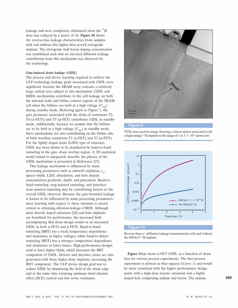
leakage and were completely eliminated when the 11Bdose was reduced by a factor of 10. Figure 10 showsthe reverse-bias leakage characteristics from sampleswith and without this higher-dose p-well retrogradeimplant. The retrograde well boron doping concentrationwas established such that no elevated diffusion leakagecontribution from this mechanism was observed forthe technology.
Gate-induced drain leakage (GIDL)The process and device learning required to achieve theULP technology leakage goals associated with GIDL weresignificant, because the SRAM array contains a relativelylarge critical area subject to this mechanism. GIDL andRBDL mechanisms contribute to the cell leakage on boththe internal node and bitline contact regions of the SRAMcell when the bitlines are held at a high voltage (VDD)during standby mode. Referring again to Figure 3, thegate perimeter associated with the drain of transistors T2,T4 (n-FETs) and T5 (p-FET) contributes GIDL in standbymode. Additionally, because we assume that the bitlinesare to be held at a high voltage (VDD) in standby mode,these mechanisms are also contributing on the bitline sideof both wordline transistors T1 (n-FET) and T2 (n-FET).For the lightly doped drain (LDD) type of structure,GIDL has been shown to be dominated by band-to-bandtunneling in the gate– drain overlap region. A 2D analyticalmodel found to adequately describe the physics of theGIDL mechanism is presented in Reference [25].
This leakage mechanism is influenced by manyprocessing parameters such as sidewall oxidation, tox,spacer width, LDD, silicidation, and halo dopantconcentration gradients, depth, and placement. Band-to-band tunneling, trap-assisted tunneling, and interface-state-assisted tunneling may be contributing factors to theoverall GIDL observed. Because the gate-bounded leakageis known to be influenced by many processing parameters,more learning with respect to these elements is clearlycritical to obtaining ultralow-leakage CMOS. Althoughmore heavily doped extension [26] and halo implantsare beneficial for performance, the increased fieldaccompanying that drain design results in an increasedGIDL in both n-FETs and p-FETs. Band-to-bandtunneling (BBT) has a weak temperature dependenceand dominates at higher voltages, while band-to-defecttunneling (BDT) has a stronger temperature dependenceand dominates at lower biases. High-performance designstend to have higher fields, which increases the BBTcomponent of GIDL. Defects and interface states are alsogenerated with these higher-dose implants, increasing theBDT component. The ULP device design goal was toreduce GIDL by minimizing the field at the drain edgeand at the same time retaining optimum short-channeleffect (SCE) control and low series resistance.
Figure 11(a) shows n-FET GIDL as a function of drainbias for various process experiments. The first processexperiment is plotted as blue squares (Curve 1) and wouldbe more consistent with the higher-performance designpoint, with a high-dose arsenic extension and a highlydoped halo comprising indium and boron. The indium
Figure 9
TEM cross-section image showing a silicon defect associated with
a high-energy 11B implant in the range of 1 to 5 � 1014 atoms/cm2.
0.2 m�
Figure 10
Reverse-bias n+ diffusion leakage measurements with and without
the 600-keV 11B implant.
n-F
ET
juncti
on l
eakage (p
A/
m2)
�
0 1 2 3 4 5
10
1
0.1
0.01
0.001
0.0001
105
Drain bias (V)
600 keV, 1 � 1014 B
No 600-keV I/I
IBM J. RES. & DEV. VOL. 47 NO. 5/6 SEPTEMBER/NOVEMBER 2003 R. W. MANN ET AL.
559

was removed from the halo, as indicated by the greendiamonds (Curve 2), resulting in roughly an order ofmagnitude reduction in GIDL. Curve 3 (navy triangles)shows further reduction in GIDL, with phosphorus addedto the extension and an increased implant angle for theboron halo. The arsenic extension dose was reducedfurther, as shown by Curve 4 (pink inverted triangles).The data points along the fifth curve (brown stars) exhibitthe lowest amount of GIDL, with arsenic completelyeliminated from the extension (phosphorus extension anda high implant tilt angle for the boron halo). It is clearlydemonstrated that, by tailoring the halo and extensions,both the magnitude and the drain-bias-dependent slopecan be significantly reduced for the n-FET.
The process experiment consistent with the higher-performance wafer containing indium in the halo showeda very weak gate-bias dependence, which suggests that theleakage is occurring deeper in the extension region, belowthe influence of the gate-induced surface potential. Asthe n-FET junction was graded further (n-FET GIDLcurves 2–5), the gate-bias dependence decreased and thetemperature dependence increased, suggesting reduced
BBT and increased BDT components. The phosphorus-only extension (Curve 5) had a temperature dependenceconsistent with a mid-gap generation trap (Ea � 0.56 eVat Vd � 1.0 V) and had a very small BBT component, asindicated by a weak drain-bias dependence. A phosphorus-only extension produced optimum GIDL results, but thisdesign point was not selected for the ULP technologybecause it also exhibited higher series resistance andwas found to show prompt-shift under hot-carrier stress.
Figure 11(b) shows the p-FET GIDL as a function ofdrain bias for various process experiments conducted. Thedata corresponding to Curve 1 (blue squares) exhibits thecharacteristics of the higher-performance design point,with Sb as the Vt adjust implant, a high-dose BF2
extension, and a highly doped As halo. The resultsindicated by Curve 2 (green diamonds) resulted when Sbwas removed and the boron halo dose was reduced. Stillfurther reduction in GIDL was obtained with a reducedBF2 halo, as shown by Curve 3 (navy triangles). Anincreased halo implant angle along with a small dosereduction resulted in the behavior modeled by Curve 4(pink inverted triangles). A reduced extension dose andincreased energy to grade the junction, coupled with thehigher halo implant angle, produced Curve 5 (brown circles).In general, the p-FET experiments showed less improvementin GIDL with junction grading than the n-FET experiments.The drain bias dependence for the p-FETs remained higheven for low bias levels, and the gate bias dependence issignificantly higher than for the n-FETs.
The higher-performance p-FET device experimentalprocess, like its n-FET counterpart, showed a very weakgate-bias dependence. This could be explained by the factthat the Sb well implant produces a super-steep retrograde(SSR) well profile that increases the field deeper in thesilicon, below the gate bias control. In contrast to then-FET, there was little change in the temperature or biasvoltage dependence for the p-FET as the junction wasgraded further (Curves 2–5). In general, the magnitude ofthe p-FET bias dependence (gate and drain) was greaterthan that of the n-FET, and the total reduction in GIDLacross the experiments was less (a reduction of about threeorders of magnitude) for the n-FET compared with areduction of less than two orders of magnitude for the p-FET.
A surprising observation made during the course of thiswork was that GIDL was found to exhibit a geometricdependence and to be dependent upon the device widthfor n-FET and p-FET. The n-FET GIDL was found toincrease by �3� with reduced channel width, while thep-FET increased by 1.5–2�. GIDL is plotted in Figure 12as a function of channel width, showing the increase thatmust be taken into account for the narrow devices in theSRAM cell. Although the precise mechanism for thiseffect is not completely apparent, it is speculated that
Figure 11
GIDL as a function of drain bias for various halo and extension
implant experiments: (a) for n-FET; (b) for p-FET.
0.5 1.0 1.5 2.0
Drain bias with Vg
� 0 V
(a)
0.1
1
10
100
1000
10000
100000High performance
No indium
Add phosphorus
Reduce arsenic
Remove arsenic
0.5 1.0 1.5 2.0
Drain bias with Vg
� 0 V
(b)
0.1
1
10
100
1000
10000
GID
L (
fA/
m)
High performance
Remove antimony
Lower halo implant
High-angle halo implant
Graded junction
2
34
5
1
2
3
4
5
1
�G
IDL
(fA
/ m
)�
R. W. MANN ET AL. IBM J. RES. & DEV. VOL. 47 NO. 5/6 SEPTEMBER/NOVEMBER 2003
560

the silicon stress associated with the STI boundary isinfluencing the dopant diffusion such that the effectiveelectric field is higher near the STI boundaries. As in thecase of NCE, this observation results in an increasedchallenge in scaling the ULP technologies to deep-submicron design nodes.
n�/p� leakagePunchthrough leakage associated with n�/p� space isprimarily a function of both the well doping concentrationand profile and the STI depth. This leakage mechanism ischaracterized as a function of n� to n-well and p� top-well space. For voltages beyond punchthrough voltage,the current increases exponentially with applied voltageas the barrier is lowered at the emitter side.
The n� to n-well and p� to p-well leakage must bekept very low for ULP applications. The contribution inleakage on a per-cell basis is less than 1 fA/�m across thevoltage range of interest down to a spacing of 0.18 �m forn� to n-well and p� to p-well. To resolve this leakage tothe cell level, one must determine the fraction of the cellwidth for which this leakage can occur. For the cell designas shown in Figure 1, this factor is approximately one halfthe total cell width. This is because, for the high internalnode, the n� diffusion to the adjacent n-well region,which is held at a high voltage (VDD), and conversely, thep� diffusion to the adjacent p-well region, which is heldat a low potential (ground) by the latch operation, are atheld the same potential during standby.
Array leakageTo measure the SRAM array leakage and betterunderstand the impacts of various process conditions onthe array standby power, an array leakage monitor (ALM)was designed. One of the unique advantages of the ALMwas that all of the support circuitry associated with the
SRAM addressing and read/write operations could beeliminated. This method for characterizing the arrayleakage was found to provide a greater degree of flexibilityin analyzing the sources of leakage in the array than astandard functional array. The ALM contained an arrayof cells electrically connected in parallel with the VDD,ground, bitline (BL) true, BL complement, and thewordline (WL) wired out to pads. With power supplied tothe array, the bitlines held high, and the wordline heldlow, the sum of all leakage mechanisms active in theSRAM cell could be measured. Measurements were madeat 1.2 V and 1.5 V for 25�C and 85�C.
The cell leakage as measured with the ALM wassuccessfully predicted using device measurements taken atthe first metal level. The method used as shown in Table 2was to sum columns at 25�C or 85�C to account for thetotal array leakage at these respective temperatures. The
Measured narrow-channel-width effect on GIDL for n-FET (squares)
and p-FET (triangles). GIDL increases as channel width is reduced
for both devices.
Figure 12
p-FET
n-FET
0.1 0.2 0.3 0.4 0.5 0.6 0.7 0.8 0.9 1.0
100
10
1
GID
L (f
A/
m)
�
Device width ( m)�
Table 2 Procedure for calculating SRAM array leakage at 25�C and 85�C.
Leakagemechanism
Leakagedetermination
Leakage percell
Array
25�C 85�C
WL n-FET Ioff Eq. (2) WWL No. of cells � Eq. (4) C(T)PD n-FET Ioff Eq. (2) WPD No. of cells � Eq. (4) C(T)PU p-FET Ioff Eq. (2) WPU No. of cells � Eq. (4) C(T)n-FET Ig Eq. (1) WPD � LPD No. of cells Ig(T)p-FET Ig Eq. (1) WPU � LPU No. of cells Ig(T)n-FET Igidl Measurement 3WWL � WPD No. of cells Igidln(T)p-FET Igidl Measurement WPU No. of cells Igidlp(T)n-FET Irbdl Measurement ABL � APD No. of cells Idiffn(T)p-FET Irbdl Measurement APU No. of cells Idiffp(T)n�/n-well current Measurement Rcell � Wcell No. of cells Rn(T)p�/p-well current Measurement Rcell � Wcell No. of cells Rp(T)
W � widthL � length
A � areaR � resistance
WL � wordlineBL � bitline
PD � pull-downPU � pull-up
g � gategidl � gate-induced drain leakage
rbdl � reverse-bias diffusion leakagediff � diffusion
IBM J. RES. & DEV. VOL. 47 NO. 5/6 SEPTEMBER/NOVEMBER 2003 R. W. MANN ET AL.
561

correlation between the predicted and measured valuesusing this straightforward approach was consideredadequate. By resolving the various leakage components tothe cell dimensions and summing the components of cellleakage obtained at the first metal level, an understandingof the dominant leakage mechanisms can be obtained. Thecalculated leakage components using the method outlinedin Table 2 are shown in Figure 13 along with themeasured array values.
SummaryAn industry-leading, low-cost, ultralow-standby-powertechnology has been developed for foundry applicationsrequiring low-power standalone or embedded SRAM in0.18-�m and 0.13-�m lithography nodes. Because theULP technology leakage goals are roughly three ordersof magnitude lower than those for the standard high-performance technology, significant learning was requiredto achieve the array leakage that was demonstrated. Adescription of the work required to achieve the GIDLtargets has been presented. In addition to the well-knowngate-oxide leakage limitations, three unique challenges forfuture scaled ULP technologies have been described.These include channel-size-dependent threshold voltagevariations and channel width dependence on both devicethreshold (NCE) and GIDL. We believe this to be thefirst literature account of the dependence of channel widthon GIDL.
Key leakage components and paths within the 6TSRAM cell have been identified and evaluated; theseinclude gate tunneling, GIDL, junction leakage,subthreshold leakage, and n�/p� punchthrough leakage.The components of SRAM cell leakage have been
quantified and accounted for in the context of theelectrical operation of the cell; when these are resolvedto the cell dimensions, good agreement between themeasured and predicted leakage is observed. Arrayleakage consistent with less than 50 fA/cell at 1.5�C,25�C and less than 400 fA/cell at 1.5 V, 85�C has beendemonstrated in both 0.18-�m and 0.13-�m-technologynodes.
AcknowledgmentThe authors wish to thank their colleagues at the IBMBurlington facility and the SRDC, R. Larsen for hishelpful comments, and T. C. Chen for his support forthis work.
References1. C. C. Wu, C. H. Diaz, B. L. Lin, S. Z. Chang, C. C.
Wang, J. J. Liaw, Ch. H. Wang, K. K. Young, K. H.Lee, B. K. Liew, and J. Y. C. Sun, “Ultra-Low Leakage0.16 �m CMOS for Low-Standby Power Applications,IEDM Tech. Digest, pp. 671– 674 (1999).
2. C. H. Diaz, M. Chang, W. Chen, M. Chiang, H. Su, S.Chang, P. Lu, C. Hu, K. Pan, C. Yang, L. Chen, C. Su, C.Wu, C. H. Wang, C. C. Wang, J. Shih, H. Hsieh, H. Tao,S. Jang, M. Yu, S. Shue, B. Chen, T. Chang, C. Hou,B. K. Liew, K. H. Lee, and Y. C. Sun, “A 0.15 �mCMOS Foundry Technology with 0.1 �m Devices forHigh Performance Applications,” Digest of TechnicalPapers, Symposium on VLSI Technology, 2000, pp.146 –147.
3. J. H. Jang, H. S. Kim, H. C. Baek, J. J. Na, K. H. Lee,D. S. Seo, K. J. Kim, K. T. Kim, Y. S. Shin, and C. G.Hwang, IEDM Tech. Digest, p. 579 (2000).
4. L. K. Han, S. Biesemans, J. Heidenreich, K. Houlihan, C.Lin, V. McGahay, T. Schiml, A. Schmidt, U. P. Schroeder,M. Stetter, C. Wann, D. Warner, R. Mahnkopf, and B.Chen, “A Modular 0.13 �m Bulk CMOS Technology forHigh Performance and Low Power Applications,” Digestof Technical Papers, Symposium on VLSI Technology, 2000,pp. 12–13.
5. A. Chatterjee, J. Esquivel, S. Nag, I. Ali, D. Rogers,K. Taylor, K. Joyner, M. Mason, D. Mercer, A.Amerasekera, T. Houston, and I. C. Chen, “A ShallowTrench Isolation Study for 0.25/0.18 �m CMOSTechnologies and Beyond,” Digest of TechnicalPapers, Symposium on VLSI Technology, 1996,pp. 156 –157.
6. F. S. Shoucair, “Scaling, Subthreshold, and LeakageCurrent Matching Characteristics in High-Temperature(25�C–250�C) VLSI CMOS Devices,” IEEE Trans.Components, Hybrids, Manuf. Technol. 12, No. 4,780 –788 (December 1989).
7. W.-C. Lee and C. Hu, “Modeling CMOS TunnelingCurrents Through Ultrathin Gate Oxide Due toConduction- and Valence-Band Electron and HoleTunneling,” IEEE Trans. Electron Devices 48, No. 7,1366 –1373 (July 2001).
8. T. Wang, L.-P. Chiang, N.-K. Zous, C.-F. Hsu, L.-Y.Huang, and T.-S. Chao, “A Comprehensive Study ofHot Carrier Stress-Induced Drain Leakage CurrentDegradation in Thin-Oxide n-MOSFETs,” IEEETrans. Electron Devices 46, No. 9, 1877–1882(September 1999).
9. J. Chen, T. Y. Chan, I. C. Chen, P. K. Ko, and C. Hu,“Subbreakdown Drain Leakage Current in MOSFET,”IEEE Electron Device Lett. 8, 515–517 (1987).
Prediction of array leakage as a function of the mean of the meas-
ured total array leakage at 25�C and 85�C at 1.5 V across a range of
hardware. Wafers more recently measured reflect the learning de-
scribed in this paper.
0.001
0.01
0.1
1
10
111
Cell
leakage (p
A)
25�C prediction
Actual
85�C prediction
Actual
1 2 3 4 5 6 7 8 9 10 11 12 13 14 15 16 17 18 19
Wafer
Figure 13
85�C specification (400 fA/cell)
25�C specification (50 fA/cell)
R. W. MANN ET AL. IBM J. RES. & DEV. VOL. 47 NO. 5/6 SEPTEMBER/NOVEMBER 2003
562

10. T. Wang, T. E. Chang, C. M. Huang, J. Y. Yang, K. M.Chang, and L. P. Chiang, “Structural Effect on Band-Trap-Band Tunneling Induced Drain Leakage in n-MOSFET’s,” IEEE Electron Device Lett. 16, No. 12,566 –568 (1995).
11. D. S. Wen, S. H. Goodwin-Johansson, and C. M. Osburn,“Tunneling Leakage in Ge-Preamorphized ShallowJunctions,” IEEE Trans. Electron Devices 35, No. 7,1107–1114 (July 1988).
12. S. H. Pyi, I. S. Yeo, D. H. Weon, Y. B. Kim, H. S. Kim,and S. K. Lee, “Roles of Sidewall Oxidation in theDevices with Shallow Trench Isolation,” IEEE ElectronDevice Lett. 20, No. 8, 384 –386 (1999).
13. W. T. Kang, J. S. Kim, K. Y. Lee, Y. C. Shin, T. H.Kim, Y. J. Park, and J. W. Park, “The Leakage CurrentImprovement in an Ultrashallow Junction NMOS with CoSilicided Source and Drain,” IEEE Electron Device Lett.21, No. 1, 9 –11 (January 2000).
14. S. M. Jung, S. B. Kim, J. S. Uom, W. S. Cho, J. Y. Kim,and K. T. Kim, “High Density Low Power Full CMOSSRAM Cell Technology with STI and CVD Ti/TiNBarrier Metal,” Proceedings of the 6th InternationalConference on VLSI and CAD, 1999, pp. 119 –121.
15. O. Bula, D. Cole, E. Conrad, D. Coops, W. Leipold, andR. Mann, “Optimization Criteria for SRAMDesign—Lithography Contribution,” Proc. SPIE 3679,No. II, 847– 859 (1999).
16. M. Lee, W.-I. Sze, and C.-M. Wu, “Static Noise Marginand Soft-Error Rate Simulations for Thin Film TransistorCell Stability in a 4 Mbit SRAM Design,” Proceedings ofthe IEEE International Symposium on Circuits and Systems(ISCAS’95), Vol. 2, 1995, pp. 937–940.
17. D. M. Kwai, H. W. Chang, H. J. Liao, C. H. Chiao,and Y. F. Chou, “Detection of SRAM Cell Stability byLowering Array Supply Voltage,” Proceedings of theNinth Asian Test Symposium, 2000, pp. 268 –273.
18. T. Hook, M. Breitwisch, J. Brown, P. Cottrell, D.Hoyniak, C. Lam, and R. Mann, IEEE Trans. ElectronDevices 49, No. 8, 1499 –1501 (August 2002).
19. A. Ono, R. Ueno, and I. Sakai, “TED Control Technologyfor Suppression of Reverse Narrow Channel Effect in0.1�m MOS Devices,” IEDM Tech. Digest, 1997, pp. 227–230.
20. J. Kim, T. Kim, J. Park, W. Kim, B. Hong, and G. Yoon,“A Shallow Trench Isolation Using Nitric Oxide (NO)-Annealed Wall Oxide to Suppress Inverse Narrow WidthEffect,” IEEE Electron Device Lett. 21, No. 12, 575–577(2000).
21. A. Asenov and S. Saini, “Suppression of Random DopantInduced Threshold Voltage Fluctuations in Sub-0.1�mMOSFET’s with Epitaxial and Delta-Doped Channels,”IEEE Trans. Electron Devices 46, No. 8, 1718 –1724 (1999).
22. A. J. Bhavnagarwala, X. Tang, and J. Meindl, “TheImpact of Intrinsic Device Fluctuations on CMOS SRAMCell Stability,” IEEE J. Solid-State Circuits 36, No. 4, 658 –665 (2001).
23. K. Takeuchi, “Channel Size Dependence of Dopant-Induced Threshold Voltage Fluctuation,” Digest ofTechnical Papers, Symposium on VLSI Technology, 1998,p. 72.
24. A. Steegen, A. Lauwers, M. de Potter, G. Badenes, R.Rooyackers, and K. Maex, “Silicide and Shallow TrenchIsolation Line Width Dependent Stress Induced JunctionLeakage,” Digest of Technical Papers, Symposium on VLSITechnology, 2000, pp. 180 –181.
25. S. A. Parke, J. E. Moon, H. C. Wann, P. K. Ko, and C.Hu, “Design for Suppression of Gate-Induced DrainLeakage in LDD MOSFET’s Using a Quasi-Two-Dimensional Analytical Model,” IEEE Trans. ElectronDevices 39, No. 7, 1694 –1703 (1992).
26. C. M. Osburn, I. De, and A. Srivastava, “Design andIntegration Considerations for End-of-the-RoadmapUltrashallow Junctions,” J. Vac. Sci. Technol. B 18,No. 1, 338 –345 (January/February 2000).
Received October 23, 2002; accepted for publicationApril 16, 2003
IBM J. RES. & DEV. VOL. 47 NO. 5/6 SEPTEMBER/NOVEMBER 2003 R. W. MANN ET AL.
563

Randy W. Mann IBM Microelectronics Division, Burlingtonfacility, 1000 River Road, Essex Junction, Vermont 05452([email protected]). Mr. Mann is a Senior Engineer inTechnology Development and Process Integration; he receivedhis B.S. degree from the University of North Carolina atGreensboro and his M.S. degree from the University of NotreDame in 1982. In 1982 he joined IBM in Essex Junction,Vermont, where he has worked in technology development onhigh-performance CMOS logic, embedded DRAM, and bothembedded and standalone SRAM applications. He currentlyholds more than 40 patents and has authored or co-authoredmore than 30 technical papers across a range of topics relatedto microelectronics. In 2001 he received an IBM CorporateAward for his work on titanium silicides; he has more recentlyworked on dense SRAM in the development of ultralow-power technologies. He is currently located in East Fishkill,New York, where he is working in the IBM SRDC on thedevelopment of the high-performance 65-nm-node CMOStechnology.
W. W. (Bill) Abadeer IBM Microelectronics Division,Burlington facility, 1000 River Road, Essex Junction, Vermont05452 ([email protected]). Dr. Abadeer is a SeniorEngineer with the Quality and Reliability Engineering groupat the Burlington facility of the IBM MicroelectronicsDivision. He joined IBM at the Burlington facility in 1976,and has since worked on the reliability of semiconductordevices. Dr. Abadeer received his M.S. and Ph.D. degrees inelectrical engineering in 1970 and 1976, respectively, from theUniversity of Vermont. From 1968 to 1976, Dr. Abadeerreceived teaching and research fellowships at the Universityof Vermont. Dr. Abadeer is a member of the IEEE and ofthe Electrochemical Society; he has several publications andpatents.
Matthew J. Breitwisch IBM Microelectronics Division,1000 River Road, Essex Junction, Vermont 05452([email protected]). Dr. Breitwisch is an Advisory Engineerin the Compact Modeling group at the IBM MicroelectronicsCenter. He received a B.S. degree in physics, mathematics,and astrophysics from the University of Wisconsin at Madisonin 1994, and a Ph.D. degree in physics from Iowa StateUniversity in 1999. He subsequently joined IBM at the IBMMicroelectronics Center, where he has worked on developinglow-standby-power SRAM. He is currently working on dc andRF compact models for CMOSFETs and passive devices. Dr.Breitweisch is an author or coauthor of one patent and tentechnical papers.
O. Bula (no longer with IBM)
Jeff S. Brown IBM Microelectronics Division, Burlingtonfacility, 1000 River Essex Junction, Vermont 05452([email protected]). Mr. Brown is an Advisory Engineerwith the Device Modeling and Simulation Department. Hereceived his B.S. and M.S. degrees in electrical engineeringfrom the Georgia Institute of Technology in 1990 and 1992,respectively. He subsequently joined IBM in Essex Junction,Vermont, working in CMOS characterization. In 1995, Mr.Brown joined the Technology Development group in EssexJunction, working on device design for foundry and low-powertechnologies; since 2002, he has worked in modeling andsimulation.
Bryant C. Colwill IBM Microelectronics Division, EastFishkill facility, Route 52, Hopewell Junction, New York 12533([email protected]). Mr. Colwill received a B.S. degreein chemical engineering from the Rensselaer PolytechnicInstitute in 2000. He subsequently joined the IBMMicroelectronics Division in Essex Junction, Vermont,focusing on low-power CMOS device isolation. Currently,Mr. Colwill is a Staff Engineer working on FEOL yieldenhancements for silicon and silicon-on-isolation technologiesat the IBM 300-mm production facility in East Fishkill, NewYork.
Peter E. Cottrell IBM Microelectronics Division, Burlingtonfacility, 1000 River Road, Essex Junction, Vermont 05452([email protected]). Dr. Cottrell received his B.S., M.E.,and Ph.D. degrees from the Rensselaer Polytechnic Institutein 1968, 1970, and 1973. He has been an engineer andmanager in the IBM Microelectronics Division since then.While at IBM he has contributed to the development ofDRAM, CMOS, and BICMOS technologies with a focus ondevice design, simulation, and modeling, as well as reliability.He has authored more than 30 technical papers and holdseight patents. Dr. Cottrell is currently responsible fordeveloping devices and models for new BiCMOS technologiesfor wireless applications at IBM. He also is a DistinguishedEngineer, an IEEE Fellow, and a member of the IBMAcademy.
William G. Crocco, Jr. 115 S. Quarry Street, Ithaca, NewYork 14850 ([email protected]). Mr. Crocco has a B.S.degree in electrical engineering from Rensselaer PolytechnicInstitute. He is currently a graduate student in electrical andcomputer engineering at Cornell University. He was a summerintern in the IBM Microelectronics Division at EssexJunction, Vermont, where he worked on CMOS leakage in2001 and ASICs in 2002.
Stephen S. Furkay IBM Microelectronics Division,Burlington facility, 1000 River Road, Essex Junction, Vermont05452 ([email protected]). Mr. Furkay is an Advisory Engineerin the SiGe Predictive Modeling group at the Essex Junction,Vermont, facility, working on various aspects of technologyCAD. He received B.S. and M.S. degrees in mechanicalengineering from Pennsylvania State University in 1976 and1979, respectively, and the M.S. degree in mathematics fromthe University of Vermont in 2001. Mr. Furkay received anIBM Outstanding Technical Achievement Award in 2001and an IBM Corporate Award in 2002 for his work on theFIELDAY semiconductor device simulation program. He isthe author or coauthor of five patents and more than 20technical papers.
Michael J. Hauser IBM Microelectronics Division,Burlington facility, 1000 River Road, Essex Junction, Vermont05452 ([email protected]). Mr. Hauser is a Staff Engineerin the Technology Reliability Department at the IBM EssexJunction, Vermont, facility. He received a B.S. degree inelectrical engineering from Purdue University in 1999,subsequently joining the IBM Microelectronics Divisionin Essex Junction, where he began work on technologyqualifications. In 2000 he assumed responsibility for devicereliability simulation. Mr. Hauser is a member of the Instituteof Electrical and Electronics Engineers.
R. W. MANN ET AL. IBM J. RES. & DEV. VOL. 47 NO. 5/6 SEPTEMBER/NOVEMBER 2003
564
Terence B. Hook IBM Microelectronics Division, Burlingtonfacility, 1000 River Road, Essex Junction, Vermont 05452([email protected]). Dr. Hook received the Sc.B. degreefrom Brown University in 1980, joining IBM in East Fishkill,New York, that same year and moving to Essex Junction,Vermont, in 1981. He attended Yale University under theauspices of the IBM Resident Study Program and completedhis Ph.D. in 1986. Since returning to IBM, he has worked onbipolar, BiCMOS, and CMOS device design and processintegration. He has also worked extensively in the field ofplasma charging damage and served as Chair of the 7thAnnual Symposium on Plasma- and Process-Induced Damagein 2002. Dr. Hook currently divides his time between EssexJunction and East Fishkill, working on 90-nm CMOSdevelopment. He is the author of more than three dozentechnical publications and holds more than a dozen patents.
Dennis Hoyniak IBM Microelectronics Division, Burlingtonfacility, 1000 River Road, Essex Junction, Vermont 05452([email protected]). Mr. Hoyniak received the B.S. degreein electrical engineering and the M.S. degree in nuclearengineering from Pennsylvania State University in 1975 and1977, respectively, and the M.S. in material science from theUniversity of Vermont in 1997. In 1980 he joined IBM, wherehe has been engaged in the development of silicon-baseddevices. Mr. Hoyniak’s current work interest is in the area ofSRAM cell development.
James M. Johnson IBM Microelectronics Division,Burlington facility, 1000 River Road, Essex Junction, Vermont05452 ([email protected]). Dr. Johnson is an AdvisoryEngineer in the Device Modeling and Simulation Departmentat the IBM Essex Junction facility. He received his bachelor’sdegree from Marquette University, majoring in physics,mathematics, and philosophy, and his Ph.D. degree in physicsfrom the University of Wisconsin at Madison in 1990. Hesubsequently joined Wayne State University as a postdoctoralfellow and then became an Assistant Professor (Research).His research there was mainly in the area of high-energyparticle theory and included investigations of quarkonium,Higgs boson, and positronium formation. In 2001 Dr. Johnsonjoined IBM, where he works on TCAD device simulation andcompact model development. He is a member of the Instituteof Electrical and Electronics Engineers and the AmericanPhysical Society.
Chung Hon Lam IBM Microelectronics Division, Burlingtonfacility, 1000 River Road, Essex Junction, Vermont 05452([email protected]).
Rebecca D. Mih IBM Microelectronics Division, EastFishkill facility, Semiconductor Research and DevelopmentCenter, Route 52, Hopewell Junction, New York 12533([email protected]). Dr. Mih is Senior Manager of theFoundry Early User Hardware Group at the SemiconductorResearch and Development Center (SRDC). She receivedB.S. and M.S. degrees in electrical engineering fromWashington State University and Arizona State University,respectively, and a Ph.D. degree in materials science andengineering from the University of California at Berkeleyin 1994. She subsequently joined IBM at the SRDC, whereshe has worked in the areas of advanced lithography, BEOL
integration of low-k materials, flash memory, and early userhardware process integration and development. Dr. Mih is anauthor or coauthor of 27 patents and seven technical papers.
J. Rivard (no longer with IBM)
Atsushi Moriwaki Yasu Semiconductor Corporation, 686-1,Ichimiyake, Yasu-Cho, Yasu-Gun, Shiga, Japan. Mr. Moriwakireceived B.E. and M.E. degrees in applied mathematics andphysics from Kyoto University, Japan, in 1982 and 1984,respectively. In 1984, he joined IBM Japan at the JapanScience Institute, Tokyo, where he worked on VLSI designmethodology and parallel processing architecture. In 1993, hemoved to the Yasu Technology Application Laboratory, Shiga,Japan, where he worked on synchronous DRAM design.From 1995 to 1998 and from 2000 to 2001, Mr. Moriwakitransferred to the IBM Microelectronics Division, workingon CMOS device design at the IBM Burlington facility inEssex Junction, Vermont. In 2001, he moved to YasuSemiconductor Ltd., where he has been working on devicecharacterization.
E. Phipps (no longer with IBM)
Christopher S. Putnam IBM Microelectronics Division,Burlington facility, 1000 River Road, Essex Junction, Vermont05452 ([email protected]). Mr. Putnam joined IBM in1997 after completing the Master of Engineering degreein electrical engineering and computer science at theMassachusetts Institute of Technology. He currently worksin the IBM Microelectronics Semiconductor Research andDevelopment Center in Essex Junction, Vermont. While atIBM, he has focused on technology development activities,including functional characterization and yield learning. Mr.Putnam is currently working in the group responsible forcharacterization and implementation of electrostatic dischargeprotection on chips in the IBM advanced silicon and silicon-on-insulator semiconductor technologies.
BethAnn Rainey IBM Microelectronics Division, Burlingtonfacility, 1000 River Road, Essex Junction, Vermont 05452([email protected]). Miss Rainey is a process developmentengineer with the Analog and Mixed Signal TechnologyDevelopment group at the IBM Microelectronics Burlingtonfacility. She received her B.S. degree in chemical engineeringfrom Purdue University in 1997 and her M.S. degree inmaterials science and engineering from the University ofMichigan in 2000. Since joining IBM in 2000, she has workedon advanced low-power CMOS, FinFET, and SiGe BiCMOStechnology development. She has authored or coauthored fivetechnical papers and six patent applications.
James J. Toomey IBM Microelectronics Division, EastFishkill facility, Route 52, Hopewell Junction, New York 12533([email protected]).
IBM J. RES. & DEV. VOL. 47 NO. 5/6 SEPTEMBER/NOVEMBER 2003 R. W. MANN ET AL.
565

Mohammad Imran Younus IBM MicroelectronicsDivision, East Fishkill facility, Route 52, Hopewell Junction,New York 12533 ([email protected]). Mr. Younus is aStaff Engineer in the Characterization and Test Departmentat the IBM 300-mm manufacturing facility in HopewellJunction, New York. He received a B.S. degree in industrialelectronics from the Institute of Industrial ElectronicsEngineering (IIEE), Pakistan, in 1993 and an M.S degree inmicroelectronics from the University of Concordia, Montreal,Canada, in 2000. He subsequently joined the IBM facilityin Essex Junction, Vermont, where he worked as acharacterization engineer in the Ultralow-Power Technologydevelopment group. Mr. Younus has received an IBMInvention Achievement Award for his work on selectivesilicide blocking.
R. W. MANN ET AL. IBM J. RES. & DEV. VOL. 47 NO. 5/6 SEPTEMBER/NOVEMBER 2003
566