Embed Size (px)
Citation preview

Differential Amplifiers Differential Amplifiers

2www.analog.comwww.analog.com
Benefits of Differential Signal Processing
n The Benefits Become Apparent when Trying to get the Most Speed and/or Resolution out of a Designo Avoid Grounding/Return Noise Problemso Better Distortion/Dynamic Range
– For the same Amplitude Differential Signal the Outputs do not Swing as Close to the Rail
– Lower Distortion especially the 2ndso Analog Signals in High-performance Systems Start and End
Differential– Almost Always the Signal Source from the Real World is
Differential– High-speed ADCs Have Differential Inputs

3www.analog.comwww.analog.com
Single-ended Components Cannot Reject Ground Noise
n Each Part of the Circuit Has a Different Reference Point
n No Matter How Careful you are with Grounding High Frequency Ground Currents will Cause Some Problems which May be Difficult to Work Around
n Op Amp Can not Reject This Ground Noise
INOISEGND 1 GND 2
VSIGNAL
ZGND

4www.analog.comwww.analog.com
Differential Amps Have Effective CMRR
n Differential Signal does not Need a Reference
n Ground and Other Noise Sources are Common to Both Inputs
o CMRR of Differential Amp is Effective
INOISE
VSIGNAL
GND 2
VOCM
GND 1
VOCM
ZGND

5www.analog.comwww.analog.com
Why Differential Signal Processing is not More Common
n Differential Signals are Commonly used Today for ADC and Line Driving
n Differential Signaling is not Generally Considered for Other Uses Because:
o Discrete Differential Designs can Be Difficult to Implement– Some Applications can not Tolerate the Higher Cost
o Not Many Differential ICs are Available– Transformers must be Used
n As Speeds and Resolution Increase the Benefits of Differential Signaling Become More Necessary

www.analog.comwww.analog.com
Differential Input/Output High-speed Amps
AD8131/2/8

7www.analog.comwww.analog.com
High Speed Differential Amps for Challenging Designs
VOUT,Differential
VOCM
VOUT,Single ended
VS-
VS+
VOUT-
VOUT+
VOCM
n Differential Signal Processing Simplifies Circuit Designo Avoid Ground Noiseo 2x Dynamic Range of Op Ampso Balanced Outputs Minimize EMIo High CMRR Reduces EMI Susceptibility
n High Speed ADC Drivingo ADCs Perform Better when Driven Differentially
n Like a Voltage Feedback Op Amp:o Gain Set by Ratio of RF/RG
– Signal Gain, Filtering, Level Shifting, Buffering / Driving

8www.analog.comwww.analog.com
What’s Inside the AD8131/2/8 Diff Amps?
n Internal CM Feedback forces Forces both outputs to be balanced,
o Equal in amplitude 180° out of phase: VOUT, CM = (VOUT+ + VOUT-)/2)
– Balance is unaffected by RF/RG matching
n Differential feedback effectively creates 2 summing nodes
o Forces Both Inputs to the same voltage when the loop is closedo High Input Z, Low Output Z
4
2
5
6
1
8
3
RG
RG
RF
RF
VOCM
VOUT+
VOUT-
VIN-
VIN+

9www.analog.comwww.analog.com
Understanding How They Work w/ Alternate Circuit Configurations
n 2 Feedback Loops
o Differential feedback forces inputs to the same voltage
o Common mode Feedback forces VOUT- = -VOUT+-
n Non-inverting example:
o For RF = 0– VOut+ = VIN
– Gain = 2
n Inverting example:
o For RF = RG
o High input Z summing node– Vout- = -VIN
– Gain = 2
VOCM
RGVIN
VOUT+
VOUT-
RF
Like Non-inverting Op Amp
Like Inverting Op Amp
VOCM
RG
RF
VIN
VOUT+
VOUT-

10www.analog.comwww.analog.com
More About the VOCM Pin
n VOCM Pin separates our diff amps from other diff amp configurations
o Creates Best Available Balance @ High Frequencieso Can be used with AC signal for Modulation as well as
DC Reference Voltages
n Easy Level Shift
o From Ground Referenced Signals (+/-5V supplies) to Single +5V Supply Signals for ADCs
o Better Distortion in signal chain for +/-5V, than +5Vo Connect to the ADC reference or any other reference
voltage

11www.analog.comwww.analog.com
AD8131/2/8 vs. Dual Op Amp Configurations
n Compared to Dual Op Amp Configuration for Differential Driving:
o 2 Op Amps, G = +1 and G = -1
– Output Dynamics are Different at High Frequencies Poor output balance; EMI emissions
o No Easy Way to Change Common Mode Output Level
o Distortion Products are Additive
– AD8131/2/8 even harmonics are Nulled by the Common Mode Feedback and Odd Harmonics are low by design

12www.analog.comwww.analog.com
AD8131/2/8 vs. Transformers
n AD8131/2/8 are similar to Center-taped Transformerso Differential or Single-ended In with Differential
Out o CM Output Adjustment
n AD8131/2/8 :o Bandwidth to DCo Does not require I/O impedance matchingo Can have signal power gaino Smaller in sizeo Lower cost than most transformerso Has higher reliability
VCM

13www.analog.comwww.analog.com
Using the AD8138 in Active Filters
n Op amps have inverting and non-inverting inputs available.
n AD8138 inputs are both inverting
o Filter topologies must be inverting types.
-
+V
OCMVOUT DM
Note two feedback loops.

14www.analog.comwww.analog.com
Filter Design
n Low-pass, High-pass and Band-pass Are Possible
o Butterworth, Bessel and Chebyshev Filters can be Realized in MF filters
n MF filters are 2nd Order (conjugate pole pairs)
o Higher order filters may be realized by stacking sectionso Multiple Feedback Filter topologies provide a DC path for the
input bias current.
-
-+
Sallen Key Low Pass Multiple Feedback Low Pass
Not acceptable Acceptable
+

15www.analog.comwww.analog.com
Differential Filter Characterization
n Low Pass, High pass and band-pass active filters were designed, built and testedo As shown in the following slides, theoretical and actual results
closely agree.
n AD8138 needs Small resistor values (10-47 Ohms) in series with the feedback circuitry to prevent oscillation at approximately 300 MHz.
n AD8132 does not Require a small resistor
n Feedback capacitance greater than a few pF may result in high frequency de-stabilization of the AD8132/8.

16www.analog.comwww.analog.com
Ex.: 2 Pole Low Pass Schematic
2 Pole Low Pass ButterworthAnti-aliasing Filter, fc = 5 MHz
- In B
+ In A1.37k
-
+
100p
100p
22p
22p332
1.37k
-5V
+5V
10
10
1.37k
1.37k
332

www.analog.comwww.analog.com
Differential Input to Single-ended Out Amps AD8129/30

18www.analog.comwww.analog.com
AD8129/30 Receivers
n Active Feedback Topology, Like the AD830
o High CMRR @ High Freqo High Input Impedance
– CMRR Insensitive to Input Zo Feedback network Independent of
signal path
n Use as:
o Differential Receiver– + & - Inputs have same Dynamic
Responseo Difference Ampo High Frequency InAmp
AD8129/30
Diff In
VoutREF
Vout

19www.analog.comwww.analog.com
AD8129/30 vs. Op Amp Configurations
n Compared to Single Op Amp Differential Amp Configuration for Receivero Poor CMRR
• Unbalanced Input Impedances
• Requires resistor matching for good CMRR
n Compared to 3 Op Amp Receiver o Lots of parts and Design Time
o Extra Amps in Signal path lowers BW

20www.analog.comwww.analog.com
AD8129/30 vs. Transformers
n AD8129/30 are similar to Transformerso Differential In with Single-ended Out oOutput Reference Adjustment
n AD8129/30 :o Bandwidth to DCo Can have signal power gaino Smaller in sizeo Lower cost than most transformerso Has higher reliability
VOUT REF
Diff InVOUT

www.analog.comwww.analog.com
For Use with High-speed Converters

22www.analog.comwww.analog.com
ADCs Perform Better when Driven Differentially
AD9240 (-6dBFS, 5V span)
-90
-80
-50
0.1 0.5 1 2 5 20
Frequency [MHz]
TH
D [
dB
] Differential
-70
-60
-40
-30
0.2 10
Single-endedDifferential
n Especially as Frequency Increases

23www.analog.comwww.analog.com
AD8138 Driving an AD9224 12-bit 40 MSPS A/D on +5V Supply
n AD9224 Reference CML output drives VOCM to set optimum CM output
o Easy level shift using VOCM
n The AD8138 provides low-distortion drive on +5V or +/-5V Supplies
500
500
500
525
+5V
+5 V
AD9224
50
50
AD8138
.1.1
.1
DigitalOutputs
-5V
50ΩSource
AVDD DVDD
VINB
VINA
AVSSSENSE
CML DVSS
VOCM

24www.analog.comwww.analog.com
3V Circuit: AD8132 Driving an AD9203 10-bit 40 MSPS A/D
n AD8132 Provides +/-1V output swing on 3V supply with low distortion for low cost ADCs
n VOCM Level Shifts from Ground-referenced input
n Resistor and capacitor between Amp and ADC needed to filter Switched-input current glitches
499
499
499
523
AIN+
AIN-
AVSS DRVSS
AVDD DRVDD
+3V
VOCM
+3V
AD9203
49.9
49.920pF
20pF
1k
1k
.1.1
.1
Digital Outputs

25www.analog.comwww.analog.com
The AD8138 is the World’s Best Amplifier for Driving High-speed ADCs
0
-20
-40
-60
-80
-100
-120
[dB
]
5 10 15 20 25 30
Frequency [MHz]
• > -80dB SFDR using the AD8138 to drive the AD9226
-100
-90
-80
-70
-60
-50
0.0E+00 5.0E+06 1.0E+07 1.5E+07 2.0E+07 2.5E+07 3.0E+07 3.5E+07
Frequency-Hz
SF
DR
-dB
+ 5 V
+/-5 V
1Vp-p signal @ 20MHz SFDR over frequency
26www.analog.comwww.analog.com
Diff amps to Help Reduce Clock Jitter
n Some ADCs have Differential Clock Inputs to Minimize Ground Noise Effects on Jitter
o Ground Noise is only one source of jitter which decreases the performance of the fastest ADCs
n As Discussed before, With Differential Signals the Ground Noise becomes Common Mode
o AD8131/2/8 can be used to send the clock signal from its source into the ADC
o Isolating Analog and Digital Grounds
o Minimizing Radiated EMI

27www.analog.comwww.analog.com
Buffered Differential Out for 12-16 bit High-speed DACs
n “Virtual GND” Reduces Effect of DAC’s Nonlinear Output Impedance
o To Achieve Larger Output Power without having a large compliance voltage on the DAC Output
o When Level Shifting is Needed use VOCM
AD975XAD976X
AD813x
150Ω
150Ω
20-0mA
0-20mA
6V Diff Output
VOCM
28www.analog.comwww.analog.com
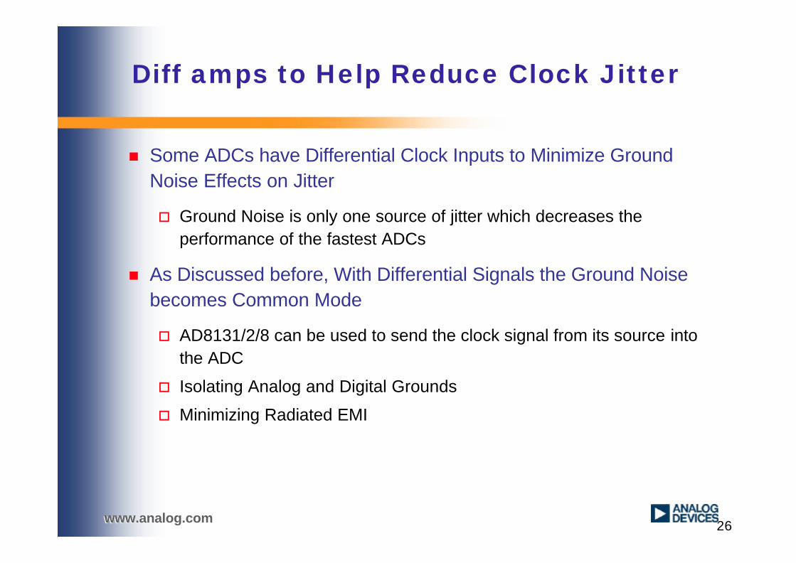
Differential to Singled-end Buffer for 12-16 bit High-speed DACs
n AD8129/30 can be used to Isolate the reactive load of the filter from the DAC output.
o Filter cap may be needed to reduce excessive slewrate on the amp input to improve amp settling
n To Achieve Larger Output Power without having a large compliance voltage on the DAC Output
o When Level Shifting is Needed use Ref input of the AD8129/30
AD975XAD976X
AD8130
20-0mA
0-20mA
L-CLPF
25Ω
CF
RG
RF
Ref Input

www.analog.comwww.analog.com
For Driving and Receiving High-speed Signals

30www.analog.comwww.analog.com
Differential Driver and Receiver
n Balanced Driver Minimizes EMI Generation
n High CMRR Receiver Minimizes EMI Pick-up
500Ω500Ω
AD8130
Vs+
Vs+
Vs-
Vs-
VfB
Vocm

31www.analog.comwww.analog.com
Cable Driving Challenge
10MHz 100MHz
-20 dB
@ 10 MHz
-60 dB
@ 100 MHz
Want Transmitter plus Receiver Response to be Inverse of Cable
1MHz100kHz
Gai
n
Frequency
0 dB
1,000 ft. (300 m)
CAT 5-UTP

32www.analog.comwww.analog.com
AD8138 Output Balance Vs Frequency
-70
-60
-50
-40
-30
-20
1 10 100 1000
+/-5V +5V
[Out
put B
alan
ce E
rror
dBc]
Frequency
Drive / Receive Requirements
n Drivero Balance needed to minimize
radiated EMIo Simple to use, no Z matching
requiredo High BW to transmit boosted
signal
n Receivero CMRR needed to reject CM Noiseo Feedback network independent of
receive sectiono High BW for equalization boost
AD8130 Common Mode Rejection vs Frequency (Vs = +/-5V, Vcm = 1Vp-p)
-120
-110
-100
-90
-80
-70
-60
-50
-40
-30
-20
0.01 0.1 1 10 100Frequency (MHz)
CM
RR
(dB
)

33www.analog.comwww.analog.com
Receive-Side Equalization
AD8129/30
Equalizing Network
Equalized Signal Out
Rf
HF Boost
Frequency
Gai
n
n Receiver Line equalizationo 40dB or more of gain can be
achieved at high frequencyo Feedback network zeros set the
gaino AD8129 has more GBWP and
Lower noise

34www.analog.comwww.analog.com
Drive Side High Frequency Boost
n Integrator on input adds zero to boost signal @ high frequency
n For Equalization when Driving Long Cables
o Gain Limited by Output swing capability
499
499
249 VOCM
+5V
49.9
49.9
-5V
249
24.9
10pF
10pF
100
Twisted -pair Cable

35www.analog.comwww.analog.com
n Useful for measuring RMS of AC Signals
n Operates to greater than 300 MHz
348
348
348
348
VOCM
+5V
49.9
-5V 50
FW Rectified Output
HP2835 (Shottky)
AD8132 Makes Simple Very High Speed Full-wave Rectifier

36www.analog.comwww.analog.com
ADI Multi-Purpose Differential Amp Family
270MHz200MHz350MHz310MHz400MHzBandwidth
1090V/µs1060V/µs1200V/µs1150V/µs2000V/µsSlew Rate
AD8130AD8129AD8132AD8138AD8131Part #
Diff-to-S.E. converter
Diff-to-S.E. converter
Low Cost Gen Purp
Best ADC DriverLine DriverPosition
1x stable10x stableAdjustable Gain / Feedback
Fixed Gain=2xFeatures
Differential-to-Single Ended ReceiverDifferential-to-Differential Driver

High-Speed Amplifiers (HSA)High-Speed Amplifiers (HSA)

38www.analog.comwww.analog.com
Fast FETs™The NEW Standard for JFET Amplifiers
n Very Easy to Use
n Negligible Ibias and I noise
n R-R output
n Wide supply range
n Low Supply Current
n Low Price

39www.analog.comwww.analog.com
n AD8033/4o 75MHz Bandwidtho 80V/µs Slew Rateo 3.2mA/Amp Typical Supply
Currento Rail-to-Rail outputo Wide Supply Range 5-24Vo Very Low Pricing
– $1.19 @ 1K - AD8033 (Single)– $1.59 @ 1K - AD8034 (Dual)
o Part Status– Final Silicon– Release QtrAD8033 (3Q02) AD8034 (2Q02)
Fast FETs™Low-Cost High-Speed AD8033/4
SOT23-8
40www.analog.comwww.analog.com
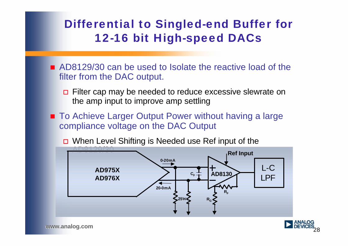
Fast FETs™High-Performance High-Speed AD8065/6
n AD8065/66
o 140MHz Bandwidtho 160V/µs Slew Rateo 7 nV/vHz Noiseo 6.5mA/Amp Typical supply currento Rail-to-Rail outputo Low offset voltage and drifto Wide Supply Range 5-24Vo Price @ 1K
– $1.59 - AD8065 (Single)– $2.29 - AD8066 (Dual)
o Part Status– Final Silicon– Release QtrAD8065 (2Q02)AD8066 (3Q02)

41www.analog.comwww.analog.com
Ultra Low-Distortion and Noise Amplifier AD8007/8
n Extremely Low SFDRo -96dB@5MHzo -86dB@20MHzo -55dB@70MHz
n Low Noise o 2.6 nV/vHzo 22 pA/vHz
n High Speedo 600MHz Bandwidtho 1000V/µs Slew Rate
n Low Powero 9mA/Amp Typical supply current
n Pricing @ 1ko $1.19 - AD8007o $1.99 - AD8008
n Part Statuso Final Silicono Release Qtr
– AD8007 (3Q02) – AD8008 (1Q03)

42www.analog.comwww.analog.com
Low-Power High-Speed Amplifier AD8038/9
n Low Powero 1.1mA/Amp Typical supply current
n High Speedo 315MHz Bandwidtho 425V/µs Slew Rate
n Low Noiseo 250pA/vHzo 7nV/vHz
n Low SFDRo -86dB @ 1MHz o -77dB @ 5MHz
n Price @ 1Ko $0.85 - AD8038o $1.20 - AD8039
n Part Statuso Final Silicono Release Qtr
– AD8038 (2Q02)– AD8039 (1Q02)

43www.analog.comwww.analog.com
Summary of New Products
Now
1Q02
1Q02
Now
1Q02
Now
Now
1Q02
Samples
1Q01Low-Power High-Speed (dual)AD8039
2Q01Low-Power High-Speed (single)AD8038
1Q03Ultra Low-Distortion and Noise (dual)AD8008
3Q02Ultra Low-Distortion and Noise (single)AD8007
3Q02Fast FETs™ High-Performance High-Speed (dual)AD8066
2Q02Fast FETs™ High-Performance High-Speed (single)AD8065
2Q02Fast FETs™ Low-Cost High-Speed (dual)AD8034
3Q02Fast FETs™ Low-Cost High-Speed (single)AD8033
ReleaseDescription Generic