Embed Size (px)
Citation preview
8/10/2019 an519
http://slidepdf.com/reader/full/an519 1/4
1 1-888-INTERSIL or 321-724-7143 | Copyright © Intersil Corporation 1999
Operational Amplifier Noise Prediction (All Op Amps)
Introduction
When working with op amp circuits an engineer is frequently
required to predict the total RMS output noise in a givenbandwidth for a certain feedback configuration. While op
amp noise can be expressed in a number of ways, “spot
noise” (RMS input voltage noise or current noise which
would pass through 1Hz wide bandpass filters centered at
various discrete frequencies), affords a universal method of
predicting output noise in any op amp configuration.
The Noise Model
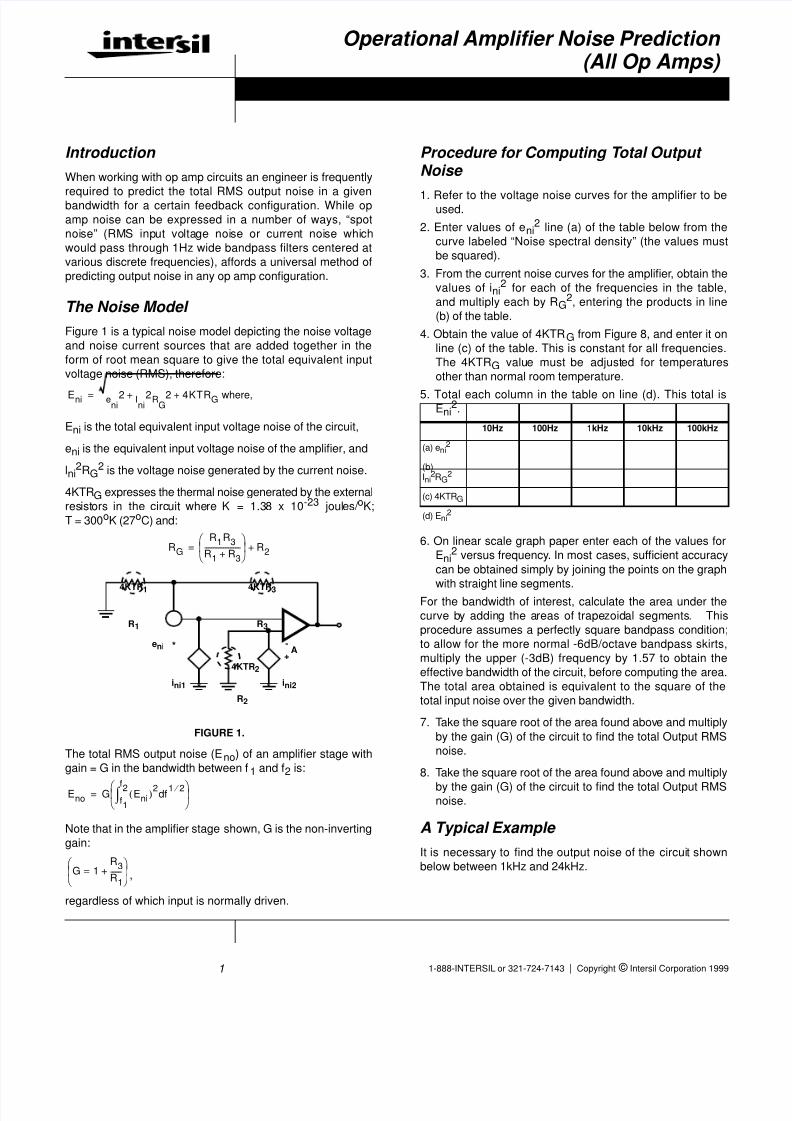
Figure 1 is a typical noise model depicting the noise voltage
and noise current sources that are added together in the
form of root mean square to give the total equivalent input
voltage noise (RMS), therefore:
Eni is the total equivalent input voltage noise of the circuit,
eni is the equivalent input voltage noise of the amplifier, and
lni2RG
2 is the voltage noise generated by the current noise.
4KTRG expresses the thermal noise generated by the external
resistors in the circuit where K = 1.38 x 10⁻²³ joules/ oK;
T = 300oK (27oC) and:
The total RMS output noise (Eno) of an amplifier stage with
gain = G in the bandwidth between f1 and f2 is:
Note that in the amplifier stage shown, G is the non-inverting
gain:
,
regardless of which input is normally driven.
Procedure for Computing Total Output Noise
1. Refer to the voltage noise curves for the amplifier to beused.
2. Enter values of eni2 line (a) of the table below from the
curve labeled “Noise spectral density” (the values must
be squared).
3. From the current noise curves for the amplifier, obtain the
values of ini2 for each of the frequencies in the table,
and multiply each by RG2, entering the products in line
(b) of the table.
4. Obtain the value of 4KTRG from Figure 8, and enter it on
line (c) of the table. This is constant for all frequencies.
The 4KTRG value must be adjusted for temperatures
other than normal room temperature.
5. Total each column in the table on line (d). This total isEni
2.
6. On linear scale graph paper enter each of the values for
Eni2 versus frequency. In most cases, sufficient accuracy
can be obtained simply by joining the points on the graph
with straight line segments.
For the bandwidth of interest, calculate the area under the
curve by adding the areas of trapezoidal segments. This
procedure assumes a perfectly square bandpass condition;
to allow for the more normal -6dB/octave bandpass skirts,
multiply the upper (-3dB) frequency by 1.57 to obtain the
effective bandwidth of the circuit, before computing the area.
The total area obtained is equivalent to the square of the
total input noise over the given bandwidth.
7. Take the square root of the area found above and multiply
by the gain (G) of the circuit to find the total Output RMS
noise.
8. Take the square root of the area found above and multiply
by the gain (G) of the circuit to find the total Output RMSnoise.
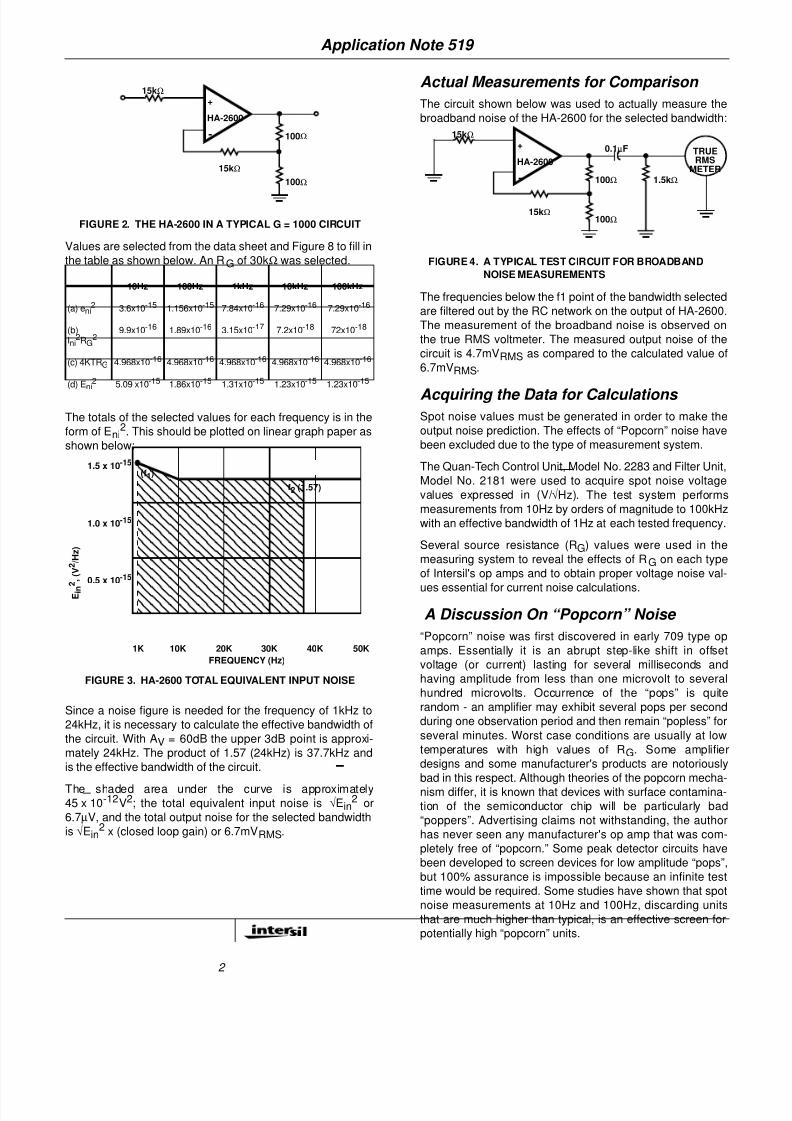
A Typical Example
It is necessary to find the output noise of the circuit shown
below between 1kHz and 24kHz.
Eni 2ni
e 2ni
I 2G
R 4KTRG+ + where,=
RG
R1R3
R1 R3+
---------------------
R2+=
FIGURE 1.
4KTR1 4KTR3
R3R1
A-
+
**
*eni
ini1
R2
4KTR2
ini2
Eno G Eni( )2df1 2 ⁄ f1
f2∫ =
G 1=
R3
R1
-------+
10Hz 100Hz 1kHz 10kHz 100kHz
(a) eni2
(b)Ini
2RG2
(c) 4KTRG
(d) Eni2
Application Note November 1996 AN519.1
8/10/2019 an519
http://slidepdf.com/reader/full/an519 2/4
2
Values are selected from the data sheet and Figure 8 to fill in
the table as shown below. An RG of 30kΩ was selected.
The totals of the selected values for each frequency is in the
form of Eni2. This should be plotted on linear graph paper as
shown below:
Since a noise figure is needed for the frequency of 1kHz to
24kHz, it is necessary to calculate the effective bandwidth of
the circuit. With AV = 60dB the upper 3dB point is approxi-
mately 24kHz. The product of 1.57 (24kHz) is 37.7kHz and
is the effective bandwidth of the circuit.
The shaded area under the curve is approximately45 x 10-12V2; the total equivalent input noise is √Ein
2 or
6.7µV, and the total output noise for the selected bandwidth
is √Ein2 x (closed loop gain) or 6.7mVRMS.
Actual Measurements for Comparison
The circuit shown below was used to actually measure the
broadband noise of the HA-2600 for the selected bandwidth:
The frequencies below the f1 point of the bandwidth selected
are filtered out by the RC network on the output of HA-2600.
The measurement of the broadband noise is observed on
the true RMS voltmeter. The measured output noise of the
circuit is 4.7mVRMS as compared to the calculated value of
6.7mVRMS.
Acquiring the Data for Calculations Spot noise values must be generated in order to make the
output noise prediction. The effects of “Popcorn” noise have
been excluded due to the type of measurement system.
The Quan-Tech Control Unit, Model No. 2283 and Filter Unit,
Model No. 2181 were used to acquire spot noise voltage
values expressed in (V/ √Hz). The test system performs
measurements from 10Hz by orders of magnitude to 100kHz
with an effective bandwidth of 1Hz at each tested frequency.
Several source resistance (RG) values were used in the
measuring system to reveal the effects of RG on each type
of Intersil's op amps and to obtain proper voltage noise val-
ues essential for current noise calculations.
A Discussion On “Popcorn” Noise
“Popcorn” noise was first discovered in early 709 type op
amps. Essentially it is an abrupt step-like shift in offset
voltage (or current) lasting for several milliseconds and
having amplitude from less than one microvolt to several
hundred microvolts. Occurrence of the “pops” is quite
random - an amplifier may exhibit several pops per second
during one observation period and then remain “popless” for
several minutes. Worst case conditions are usually at low
temperatures with high values of RG. Some amplifier
designs and some manufacturer's products are notoriously
bad in this respect. Although theories of the popcorn mecha-
nism differ, it is known that devices with surface contamina-
tion of the semiconductor chip will be particularly bad
“poppers”. Advertising claims not withstanding, the author
has never seen any manufacturer's op amp that was com-
pletely free of “popcorn.” Some peak detector circuits have
been developed to screen devices for low amplitude “pops”,
but 100% assurance is impossible because an infinite test
time would be required. Some studies have shown that spot
noise measurements at 10Hz and 100Hz, discarding units
that are much higher than typical, is an effective screen for
potentially high “popcorn” units.
10Hz 100Hz 1kHz 10kHz 100kHz
(a) eni2 3.6x10⁻¹⁵ 1.156x10⁻¹⁵ 7.84x10⁻¹⁶ 7.29x10⁻¹⁶ 7.29x10⁻¹⁶
(b)Ini
2RG2
9.9x10⁻¹⁶ 1.89x10⁻¹⁶ 3.15x10⁻¹⁷ 7.2x10⁻¹⁸ 72x10-18
(c) 4KTRG 4.968x10⁻¹⁶ 4.968x10⁻¹⁶ 4.968x10⁻¹⁶ 4.968x10⁻¹⁶ 4.968x10⁻¹⁶
(d) Eni2 5.09 x10⁻¹⁵ 1.86x10⁻¹⁵ 1.31x10⁻¹⁵ 1.23x10⁻¹⁵ 1.23x10⁻¹⁵
FIGURE 2. THE HA-2600 IN A TYPICAL G = 1000 CIRCUIT
15kΩ
15kΩ
100Ω
100Ω
+
-
HA-2600
FIGURE 3. HA-2600 TOTAL EQUIVALENT INPUT NOISE
(f1)1.5 x 10⁻¹⁵
f2 (1.57)
1.0 x 10⁻¹⁵
0.5 x 10⁻¹⁵
1K 10K 20K 30K 40K 50K
E i n
2 , ( V 2 / H z )
FREQUENCY (Hz)
FIGURE 4. A TYPICAL TEST CIRCUIT FOR BROADBAND
NOISE MEASUREMENTS
15kΩ
15kΩ
100Ω
100Ω
+
-
HA-2600
1.5kΩ
TRUERMS
METER
0.1µF
Application Note 519
8/10/2019 an519
http://slidepdf.com/reader/full/an519 3/4
3
The vast majority of Intersil op amps will exhibit less than
3µVP-P “popcorn”. Screening can be performed, but it
should be noted that the confidence level of the screen could
be as low as 60%.
References
[1] Fitchen, F.C. and Motchenbacker, C.D. Low Noise
Electronic Design. New York: John Wiley and Sons,
1973.
Instruction Manual, Model 2173C Transistor Noise Analyzer
Control Unit. Quan-Tech, Division of KMS Industries. Whip-
pany, New Jersey.
Typical Spot Noise Curves Unless Otherwise Noted: VS = ±15V, TA = 25oC
FIGURE 5. HA-2500/2510/2520 INPUT NOISE VOLTAGE FIGURE 6. HA-2500/2510/2520 INPUT NOISE CURRENT
FIGURE 7. HA-4741 INPUT NOISE VOLTAGE FIGURE 8. HA-4741 INPUT NOISE CURRENT
FIGURE 9. NOISE vs RESISTOR VALUE
10-11
10-12
10-13
10-14
10-15
10-16
10 100 1K 10K 100K
M E A N
S Q U A R E N O I S E V O L T A G E ( V 2 / H z )
FREQUENCY (Hz)
SOURCE RESISTANCE = 100kΩ
SOURCE RESISTANCE = 0Ω
SOURCE RESISTANCE = 300kΩ
10-21
10-22
10-23
10-24
10-25
10-26
100 1K 10K 100K
M E A
N
S Q U A R E N O I S E C U R R E N T ( A 2 / H z )
FREQUENCY (Hz)
10
10-14
10-15
10-16
10-17
10 100 1K 10K 100K
M E A N
S Q U
A R E N O I S E V O L T A G E ( V 2 / H z )
FREQUENCY (Hz)
SOURCE RESISTANCE = 100kΩ
SOURCE RESISTANCE = 0Ω
10-24
10-25
10-26
10-27
10 100 1K 10K 100K M E A N
S Q U A
R E N O I S E C U R R E N T ( A 2 / H z )
FREQUENCY (Hz)
10-14
10-15
10-16
10-17
1K 10K 100K 1M 10M
4 K T R G
RG (Ω)
10-13
10-12
100M
4KTRG
Application Note 519
8/10/2019 an519
http://slidepdf.com/reader/full/an519 4/4
4
All Intersil semiconductor products are manufactured, assembled and tested under ISO9000 quality systems certification.
Intersil semiconductor products are sold by description only. Intersil Corporation reserves the right to make changes in circuit design and/or specifications at any time with-
out notice. Accordingly, the reader is cautioned to verify that data sheets are current before placing orders. Information furnished by Intersil is believed to be accurate and reliable. However, no responsibility is assumed by Intersil or its subsidiaries for its use; nor for any infringements of patents or other rights of third parties which may result
from its use. No license is granted by implication or otherwise under any patent or patent rights of Intersil or its subsidiaries.
For information regarding Intersil Corporation and its products, see web site www.intersil.com
Sales Office Headquarters NORTH AMERICA
Intersil Corporation
P. O. Box 883, Mail Stop 53-204
Melbourne, FL 32902
TEL: (321) 724-7000
FAX: (321) 724-7240
EUROPE
Intersil SA
Mercure Center
100, Rue de la Fusee
1130 Brussels, Belgium
TEL: (32) 2.724.2111
FAX: (32) 2.724.22.05
ASIA
Intersil (Taiwan) Ltd.
7F-6, No. 101 Fu Hsing North Road
Taipei, Taiwan
Republic of China
TEL: (886) 2 2716 9310
FAX: (886) 2 2715 3029
Application Note 519


