Embed Size (px)
Citation preview
CAD and Design Project Course for SoC
1
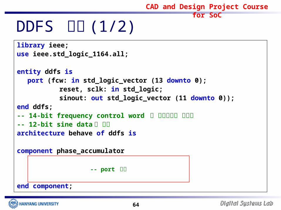
Direct Digital Frequency Synthesizer (DDFS) 소개 및
설계
Digital Systems Lab신현철 교수
CAD and Design Project Course for SoC
2
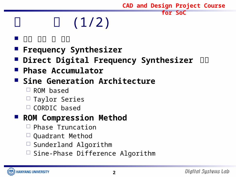
목 차 (1/2) 등장 배경 및 특징 Frequency Synthesizer Direct Digital Frequency Synthesizer 소개 Phase Accumulator Sine Generation Architecture
ROM based Taylor Series CORDIC based
ROM Compression Method Phase Truncation Quadrant Method Sunderland Algorithm Sine-Phase Difference Algorithm
CAD and Design Project Course for SoC
3
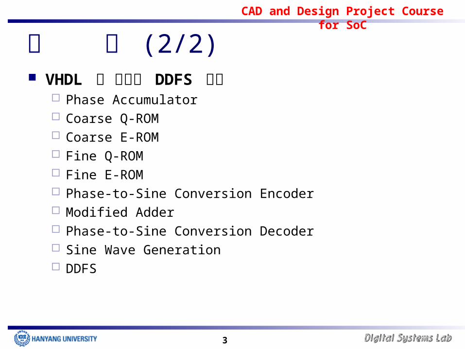
목 차 (2/2) VHDL 을 이용한 DDFS 설계
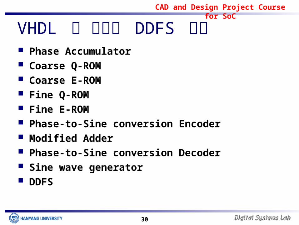
Phase Accumulator Coarse Q-ROM Coarse E-ROM Fine Q-ROM Fine E-ROM Phase-to-Sine Conversion Encoder Modified Adder Phase-to-Sine Conversion Decoder Sine Wave Generation DDFS
CAD and Design Project Course for SoC
4
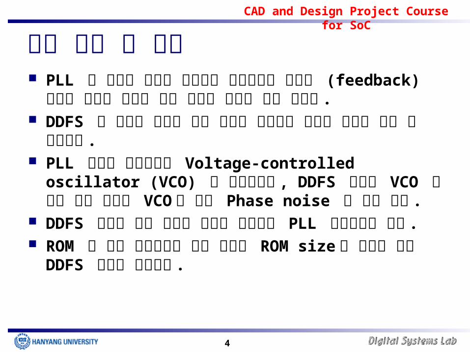
등장 배경 및 특징 PLL 을 이용한 주파수 합성기는 본질적으로 피드백
(feedback) 루프를 가지고 있어서 빠른 주파수 변환을 하기 어렵다 .
DDFS 는 피드백 루프가 없기 때문에 고속으로 주파수 변환을 하는 데 적합하다 .
PLL 주파수 합성기에는 Voltage-controlled oscillator (VCO) 가 필요하지만 , DDFS 에서는 VCO 가 필요 없기 때문에 VCO 로 인한 Phase noise 가 보다 작다 .
DDFS 에서의 출력 파형의 주파수 해상도가 PLL 합성기보다 높다 .
ROM 에 의한 소모전력이 크기 때문에 ROM size 를 줄이는 것이 DDFS 연구의 핵심이다 .
CAD and Design Project Course for SoC
5
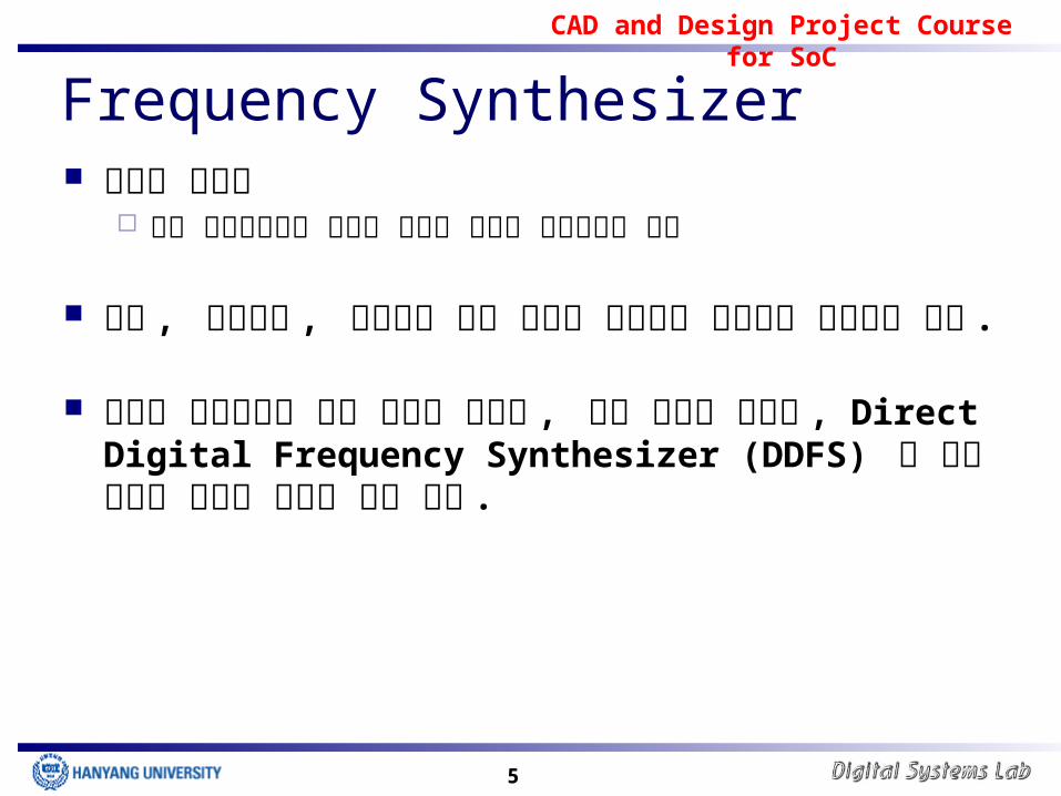
Frequency Synthesizer 주파수 합성기
기준 주파수로부터 다양한 주파수 신호를 발생시키는 장치
통신 , 계측장비 , 의료기기 등의 다양한 분야에서 중요하게 사용되고 있다 .
주파수 합성기에는 직접 주파수 합성기 , 간접 주파수 합성기 , Direct Digital Frequency Synthesizer (DDFS) 와 앞의 방식을 혼합한 혼합형 등이 있다 .
CAD and Design Project Course for SoC
6
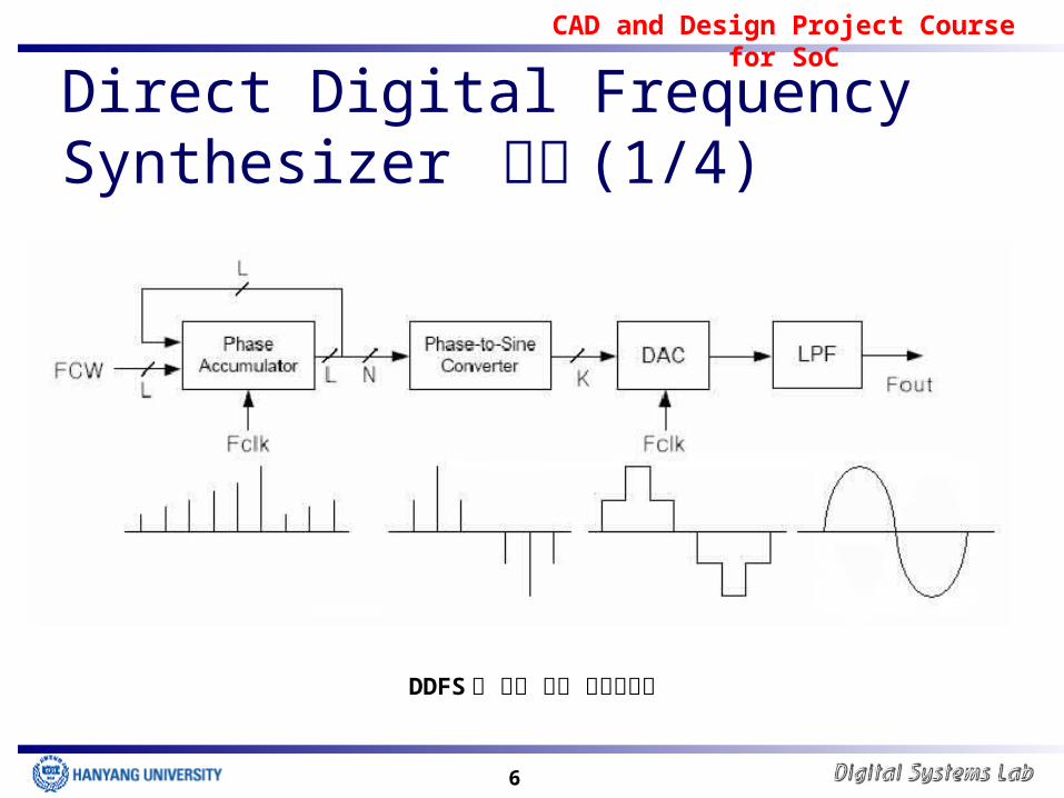
Direct Digital Frequency Synthesizer 소개 (1/4)
DDFS 의 기본 블록 다이어그램
CAD and Design Project Course for SoC
7
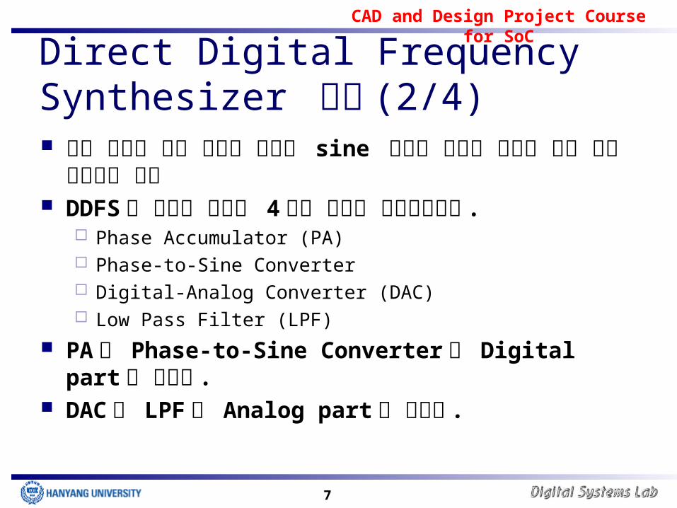
Direct Digital Frequency Synthesizer 소개 (2/4) 직접 주파수 합성 방식의 하나로 sine 파형을 디지털
회로에 의해 직접 생성하는 방법 DDFS 는 다음에 제시된 4 개의 요소로 구성되어있다 .
Phase Accumulator (PA) Phase-to-Sine Converter Digital-Analog Converter (DAC) Low Pass Filter (LPF)
PA 와 Phase-to-Sine Converter 는 Digital part 에 속한다 .
DAC 와 LPF 는 Analog part 에 속한다 .
CAD and Design Project Course for SoC
8
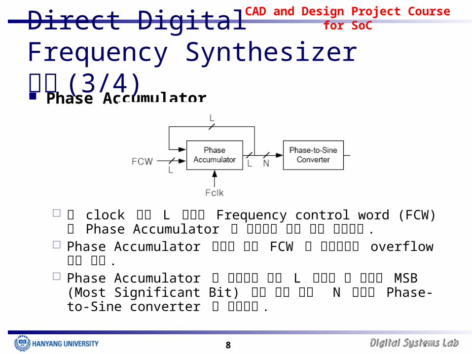
Direct Digital Frequency Synthesizer 소개 (3/4) Phase Accumulator
매 clock 마다 L 비트의 Frequency control word (FCW) 가 Phase Accumulator 에 저장되어 있는 값에 더해진다 .
Phase Accumulator 에서는 계속 FCW 가 더해지므로 overflow 하게 된다 .
Phase Accumulator 에 저장되어 있는 L 비트의 값 중에서 MSB (Most Significant Bit) 쪽에 있는 상위 N 비트가 Phase-to-Sine converter 로 입력된다 .
CAD and Design Project Course for SoC
9
Direct Digital Frequency Synthesizer 소개 (4/4) Phase-to-Sine Converter 를 구현하는 방법
ROM table 을 이용 Taylor series 를 이용 Coordinated Rotation Digital Computer (CORDIC) 을 이용
최종 출력 Phase-to-Sine Converter 의 디지털 출력 값이 DAC 를
통과하면 아날로그 값으로 변환 마지막으로 Low Pass Filter (LPF) 를 통과하면 원래의
부드러운 Sine 파형을 얻을 수 있다 .
CAD and Design Project Course for SoC
10
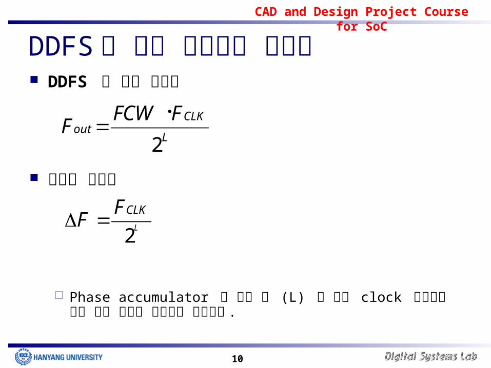
DDFS 의 출력 주파수와 해상도 DDFS 의 출력 주파수
주파수 해상도
Phase accumulator 의 비트 수 (L) 가 크고 clock 주파수가 작을 수록 주파수 해상도가 향상된다 .
2LCLK
outFFCW
F
2L
CLKFF
CAD and Design Project Course for SoC
11
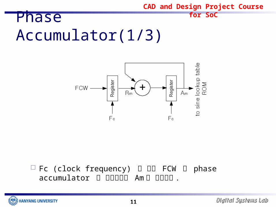
Phase Accumulator(1/3)
Fc (clock frequency) 에 따라 FCW 가 phase accumulator 로 인가되어서 Am 에 더해진다 .
CAD and Design Project Course for SoC
12
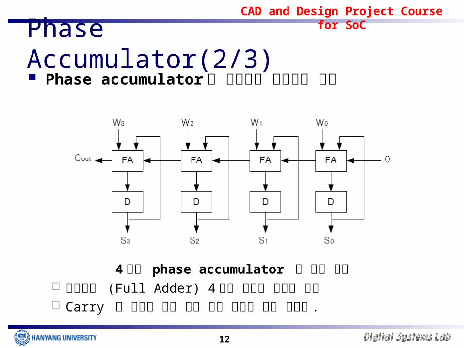
Phase Accumulator(2/3) Phase accumulator 를 구현하는 기본적인 방법
4 비트 phase accumulator 의 기본 구조 전가산기 (Full Adder) 4 개를 직렬로 연결한 구조 Carry 의 전달로 인해 전체 계산 시간이 오래 걸린다 .
CAD and Design Project Course for SoC
13
Phase Accumulator(3/3)
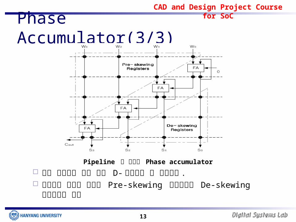
Pipeline 을 이용한 Phase accumulator
앞의 그림에서 검은 점은 D- 플립플롭 을 나타낸다 . 타이밍을 맞추기 위해서 Pre-skewing 레지스터와 De-
skewing 레지스터가 사용
CAD and Design Project Course for SoC
14
Sine Generation Architecture(1/4) ROM based
Sine wave generation 에서 해당 위상 값을 이용하여 ROM 을 look-up 하는 방식
위상 값이 ROM 의 주소 값 ROM 의 크기를 줄이는 것이 관건 Quadrant method Sunderland Algorithm Sine-phase difference Algorithm
CAD and Design Project Course for SoC
15
Sine Generation Architecture(2/4)
ROM based architecture 의 장점 구현하기 비교적 쉽다 . ROM 크기를 줄인 경우 , 전력 소모와 속도 면에서 효율적이다 .
ROM based architecture 의 단점 정밀도를 높일 수록 ROM 크기가 커진다 . ROM 크기가 클수록 속도도 느려지고 , 전력소모량도 증가한다 .
CAD and Design Project Course for SoC
16
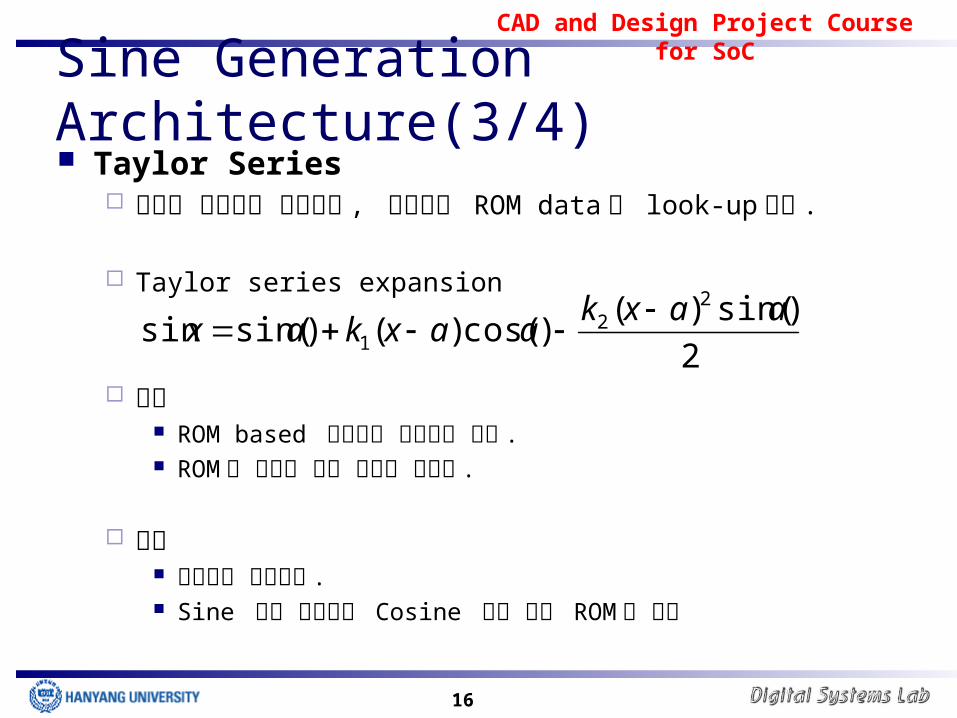
Sine Generation Architecture(3/4) Taylor Series
일부는 곱셈기를 사용하고 , 나머지는 ROM data 를 look-up한다 .
Taylor series expansion
장점 ROM based 방식보다 압축률이 좋다 . ROM 의 크기가 작기 때문에 빠르다 .
단점 곱셈기가 필요하다 . Sine 값만 구하여도 Cosine 값에 대한 ROM 이 필요
2
)sin()()cos()()sin(sin
22
1
aaxkaaxkax
CAD and Design Project Course for SoC
17
Sine Generation Architecture(4/4) CORDIC based
ROM look-up 방식을 사용하지 않음 직접 Coordinated Rotation Digital Computer (CORDIC)
연산 수행 ROM 크기에 영향을 받지 않음
장점 sin, cos 값을 동시에 발생 Pipeline 에 의한 빠른 속도
단점 복잡한 회로 높은 전력 소모
CAD and Design Project Course for SoC
18
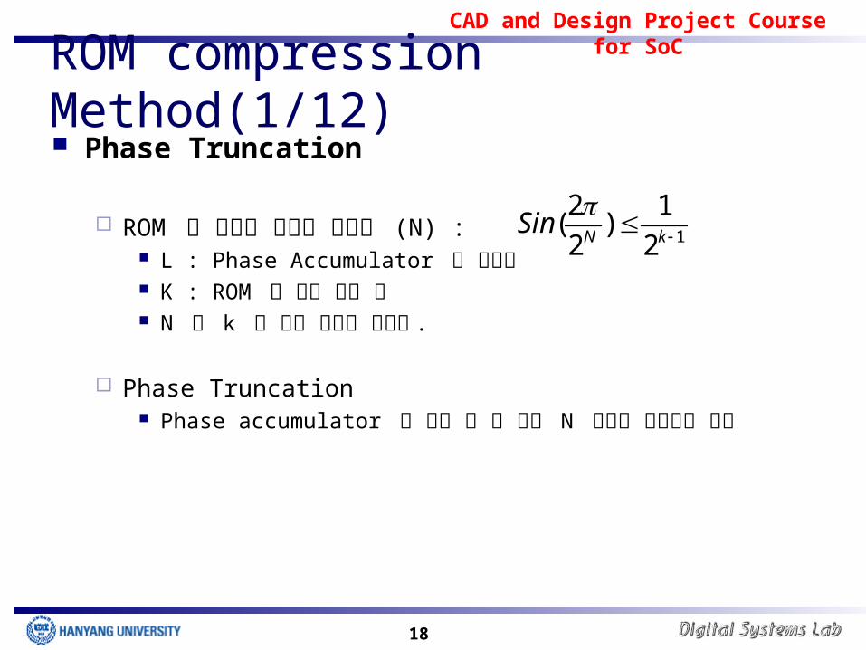
ROM compression Method(1/12) Phase Truncation
ROM 의 입력에 필요한 비트수 (N) : L : Phase Accumulator 의 비트수 K : ROM 의 출력 비트 수 N 은 k 에 의해 영향을 받는다 .
Phase Truncation Phase accumulator 의 출력 값 중 상위 N 비트만 사용하는 기법
12
1)
2
2(
kNSin
CAD and Design Project Course for SoC
19
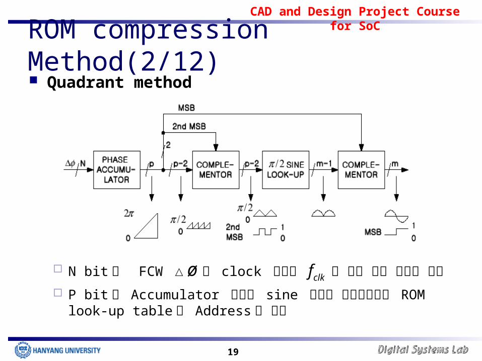
ROM compression Method(2/12) Quadrant method
N bit 의 FCW △ø 가 clock 주파수 fclk 에 의해 선형 위상을 생성
P bit 의 Accumulator 출력이 sine 파형을 생성하기위한 ROM look-up table 의 Address 로 사용
CAD and Design Project Course for SoC
20
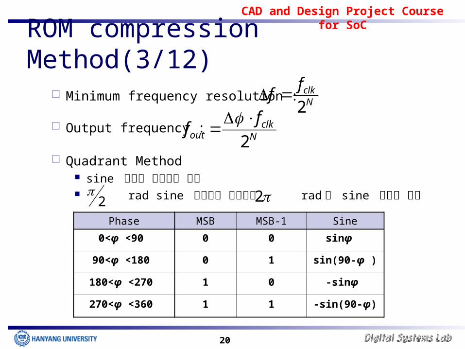
ROM compression Method(3/12)
Minimum frequency resolution :
Output frequency :
Quadrant Method sine 파형의 대칭성을 사용 rad sine 파형만을 이용해서 rad 의 sine 파형을 생성
Nclkff
2
Nclk
out
ff
2
2 2
Phase MSB MSB-1 Sine
0<φ <90 0 0 sinφ
90<φ <180 0 1 sin(90-φ )
180<φ <270 1 0 -sinφ
270<φ <360 1 1 -sin(90-φ)
CAD and Design Project Course for SoC
21
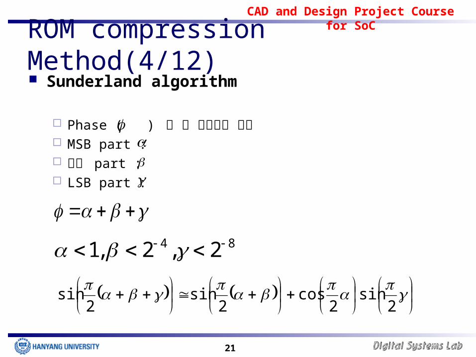
ROM compression Method(4/12) Sunderland algorithm
Phase ( ) 를 세 부분으로 나눔 MSB part : 중간 part : LSB part :
84 2,2,1
2sin
2cos
2sin
2sin
CAD and Design Project Course for SoC
22
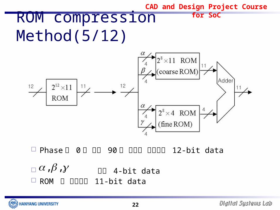
ROM compression Method(5/12)
Phase 는 0 도 에서 90 도 까지를 나타내는 12-bit data
모두 4-bit data ROM 의 출력값은 11-bit data
, ,
CAD and Design Project Course for SoC
23
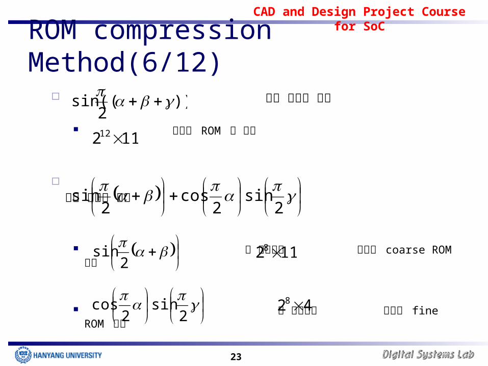
ROM compression Method(6/12)
값만 저장할 경우
크기의 ROM 이 필요
값을 저장할 경우
을 저장하는 크기의 coarse ROM 필요
을 저장하는 크기의 fine ROM 필요
))(2
sin(
11212
2sin
2cos
2sin
2sin 1128
2sin
2cos 428
CAD and Design Project Course for SoC
24
ROM compression Method(7/12)
의 값이 와 에 비하여 매우 작다 .
의 값의 상위 7 비트는 모두 0 이므로
ROM 에 저장할 필요가 없으므로 fine ROM 의 출력은 4 비트면 충
분 커다란 ROM 을 두 개의 작은 ROM 으로 나눈 형태 최종 출력값 : coarse ROM 과 fine ROM 의 출력값을 더한 값 추가적인 덧셈기가 하나 필요
2sin
2cos
CAD and Design Project Course for SoC
25
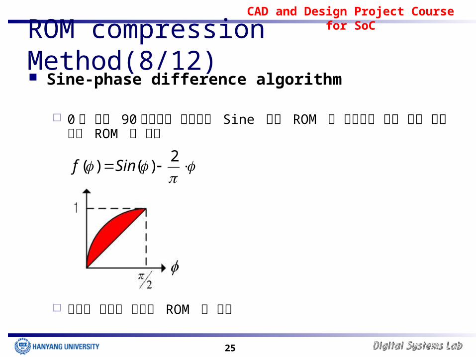
ROM compression Method(8/12) Sine-phase difference algorithm
0 도 부터 90 도까지에 해당하는 Sine 값을 ROM 에 저장하는 대신 다음 식의 값을 ROM 에 저장
색으로 표시된 부분을 ROM 에 저장
2
)()( Sinf
CAD and Design Project Course for SoC
26
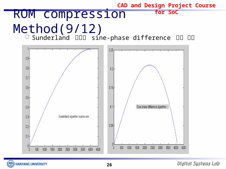
ROM compression Method(9/12)
Sunderland 방식과 sine-phase difference 방식 비교
CAD and Design Project Course for SoC
27
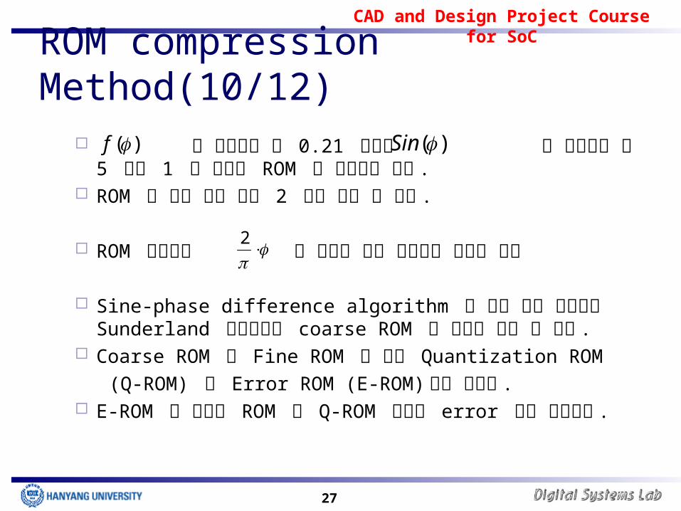
ROM compression Method(10/12)
의 최대값은 약 0.21 이므로 의 최대값의 약 5 분의 1 의 크기를 ROM 에 저장하면 된다 .
ROM 의 출력 비트 수를 2 비트 줄일 수 있다 .
ROM 출력값에 를 더하기 위해 추가적인 덧셈기 필요
Sine-phase difference algorithm 의 경우 앞의 그림처럼 Sunderland 방식에서의 coarse ROM 의 크기를 줄일 수 있다 .
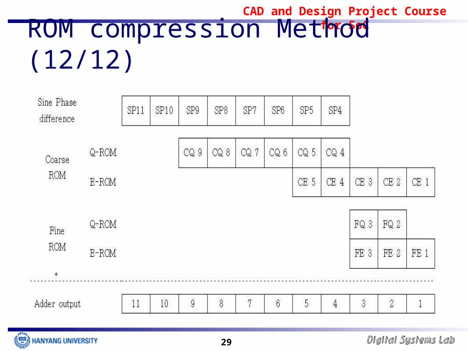
Coarse ROM 과 Fine ROM 을 다시 Quantization ROM (Q-ROM) 과 Error ROM (E-ROM) 으로 나눈다 . E-ROM 은 원래의 ROM 과 Q-ROM 사이의 error 값을
저장한다 .
)(f )(Sin
2
CAD and Design Project Course for SoC
28
ROM compression Method(11/12)
2nd MSB
MSB2
PHASE ACCUMULATOR
COMPLEMENTOR
N
p
DELAYDELAY
p-2
p-2
MODIFIED ADDER
COMPLEMENTOR
m-1
m
COARSE ROM
Q-ROM E-ROM
FINE ROM
Q-ROM E-ROM
CAD and Design Project Course for SoC
29
ROM compression Method (12/12)
CAD and Design Project Course for SoC
30
VHDL 을 이용한 DDFS 설계 Phase Accumulator Coarse Q-ROM Coarse E-ROM Fine Q-ROM Fine E-ROM Phase-to-Sine conversion Encoder Modified Adder Phase-to-Sine conversion Decoder Sine wave generator DDFS
CAD and Design Project Course for SoC
31
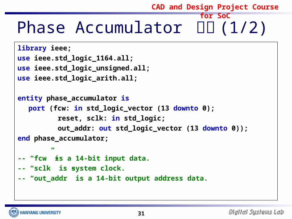
Phase Accumulator 설계 (1/2)library ieee;use ieee.std_logic_1164.all;use ieee.std_logic_unsigned.all;use ieee.std_logic_arith.all;
entity phase_accumulator isport (fcw: in std_logic_vector (13 downto 0);
reset, sclk: in std_logic;out_addr: out std_logic_vector (13 downto 0));
end phase_accumulator;
-- “fcw” is a 14-bit input data.-- “sclk” is system clock.-- “out_addr” is a 14-bit output address data.
CAD and Design Project Course for SoC
32
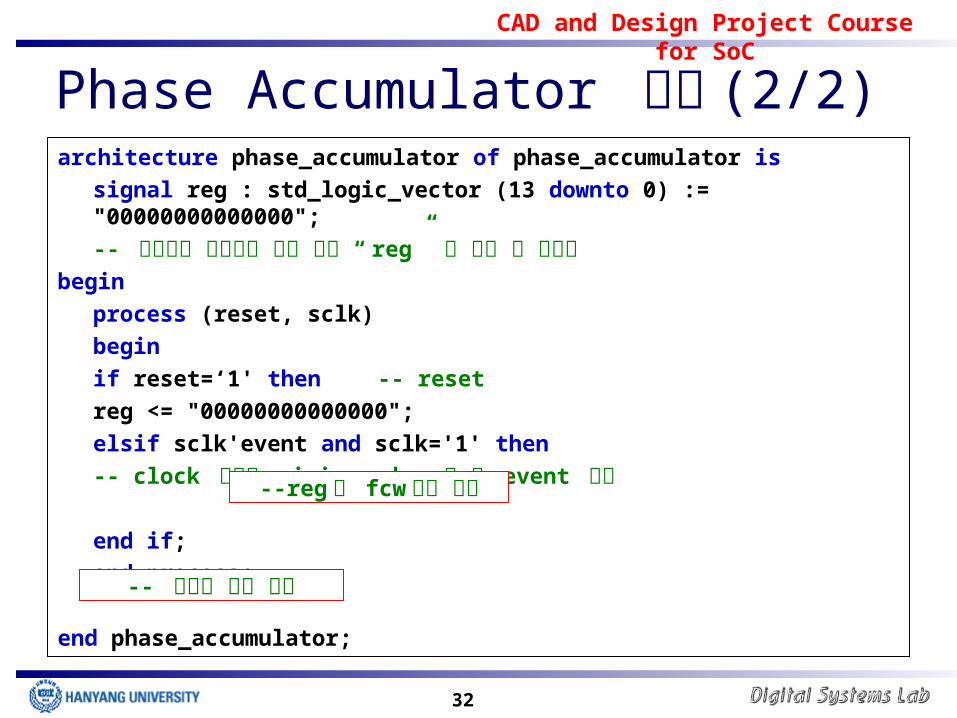
Phase Accumulator 설계 (2/2)architecture phase_accumulator of phase_accumulator is
signal reg : std_logic_vector (13 downto 0) := "00000000000000";-- 입력값을 누산하기 위한 변수 “reg” 를 선언 및 초기화
beginprocess (reset, sclk)begin
if reset=‘1' then -- reset reg <= "00000000000000";
elsif sclk'event and sclk='1' then-- clock 신호가 rising edge 일 때 event 발생
end if;end process;
end phase_accumulator;
--reg 에 fcw 값을 누산
-- 누산된 값을 출력
CAD and Design Project Course for SoC
33
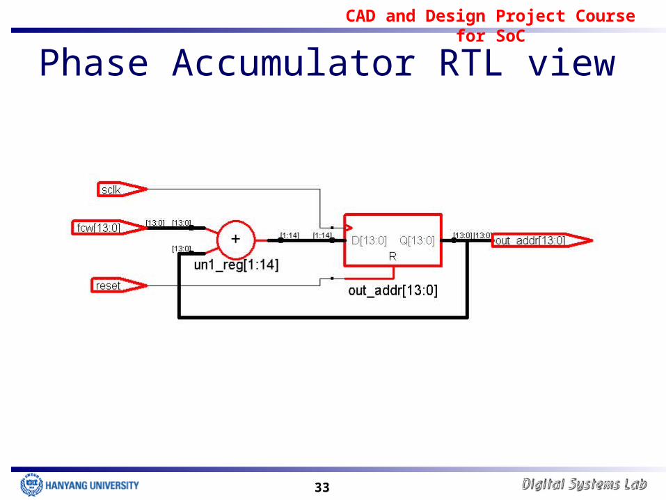
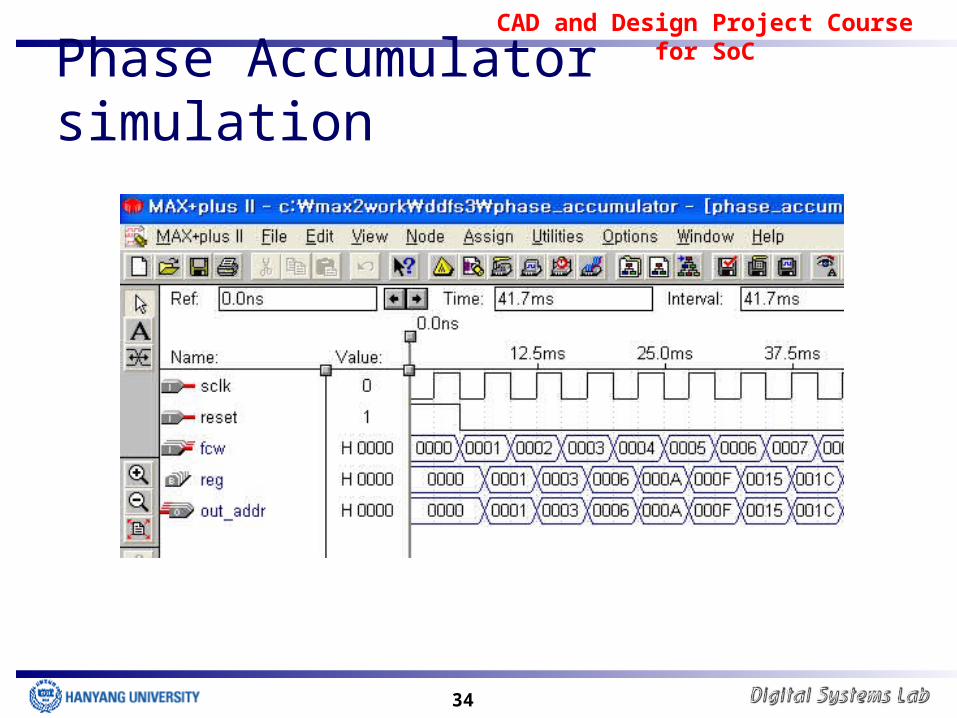
Phase Accumulator RTL view
CAD and Design Project Course for SoC
34
Phase Accumulator simulation
CAD and Design Project Course for SoC
35
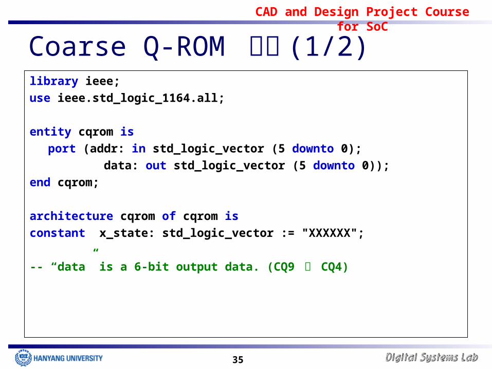
Coarse Q-ROM 설계 (1/2)library ieee;use ieee.std_logic_1164.all;
entity cqrom isport (addr: in std_logic_vector (5 downto 0); data: out std_logic_vector (5 downto 0));
end cqrom;
architecture cqrom of cqrom isconstant x_state: std_logic_vector := "XXXXXX";
-- “data” is a 6-bit output data. (CQ9 〜 CQ4)
CAD and Design Project Course for SoC
36
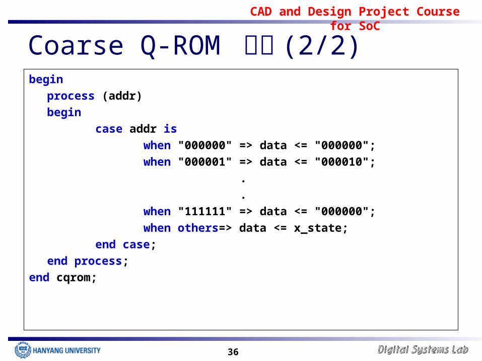
Coarse Q-ROM 설계 (2/2)begin
process (addr)begin
case addr iswhen "000000" => data <= "000000";when "000001" => data <= "000010";
.
.when "111111" => data <= "000000";when others=> data <= x_state;
end case;end process;
end cqrom;
CAD and Design Project Course for SoC
37
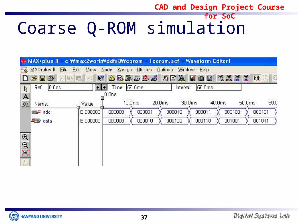
Coarse Q-ROM simulation
CAD and Design Project Course for SoC
38
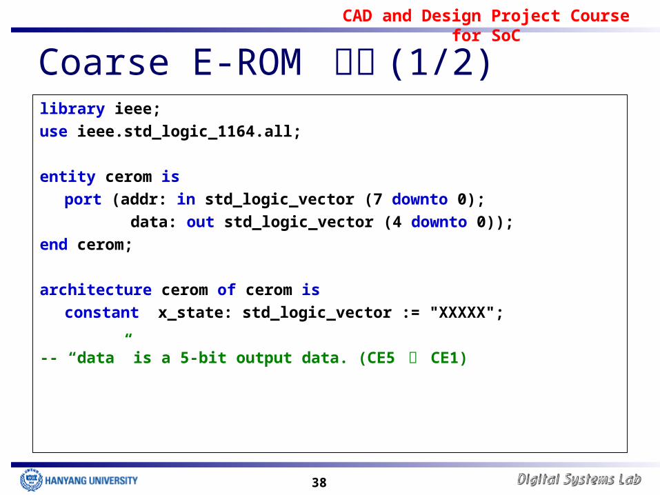
Coarse E-ROM 설계 (1/2)library ieee;use ieee.std_logic_1164.all;
entity cerom isport (addr: in std_logic_vector (7 downto 0);
data: out std_logic_vector (4 downto 0));end cerom;
architecture cerom of cerom isconstant x_state: std_logic_vector := "XXXXX";
-- “data” is a 5-bit output data. (CE5 〜 CE1)
CAD and Design Project Course for SoC
39
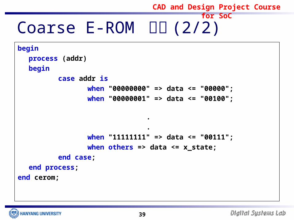
Coarse E-ROM 설계 (2/2)begin
process (addr)begin
case addr iswhen "00000000" => data <= "00000";when "00000001" => data <= "00100";
.
.when "11111111" => data <= "00111";when others => data <= x_state;
end case;end process;
end cerom;
CAD and Design Project Course for SoC
40
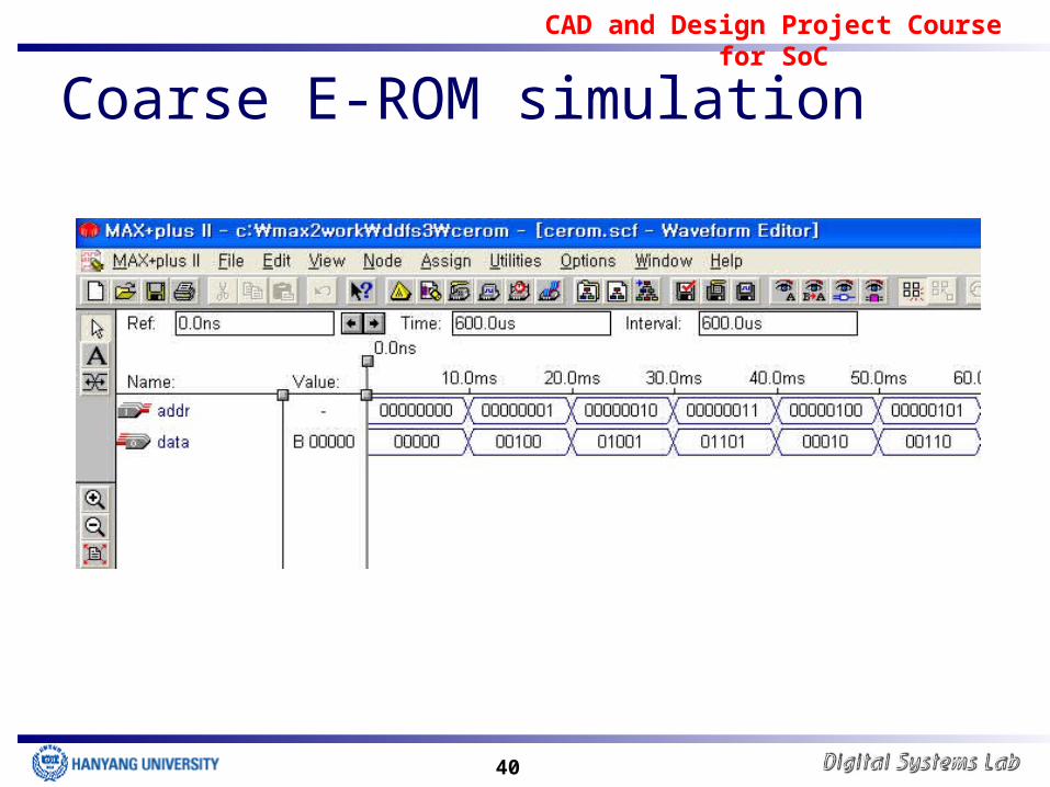
Coarse E-ROM simulation
CAD and Design Project Course for SoC
41
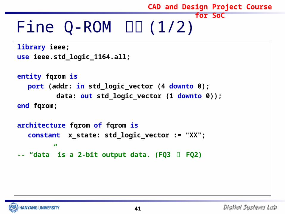
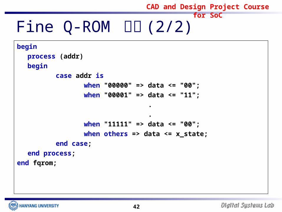
Fine Q-ROM 설계 (1/2)library ieee;use ieee.std_logic_1164.all;
entity fqrom isport (addr: in std_logic_vector (4 downto 0);
data: out std_logic_vector (1 downto 0));end fqrom;
architecture fqrom of fqrom isconstant x_state: std_logic_vector := "XX";
-- “data” is a 2-bit output data. (FQ3 〜 FQ2)
CAD and Design Project Course for SoC
42
Fine Q-ROM 설계 (2/2)begin
process (addr)begin
case addr iswhen "00000" => data <= "00";when "00001" => data <= "11";
. .
when "11111" => data <= "00";when others => data <= x_state;
end case;end process;
end fqrom;
CAD and Design Project Course for SoC
43
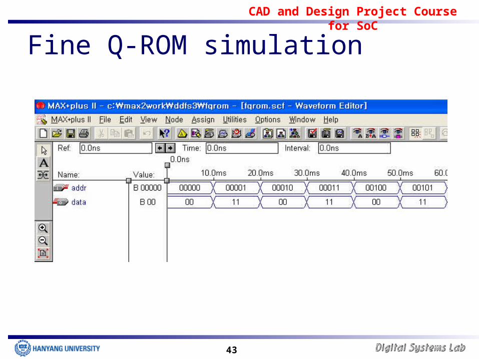
Fine Q-ROM simulation

CAD and Design Project Course for SoC
44
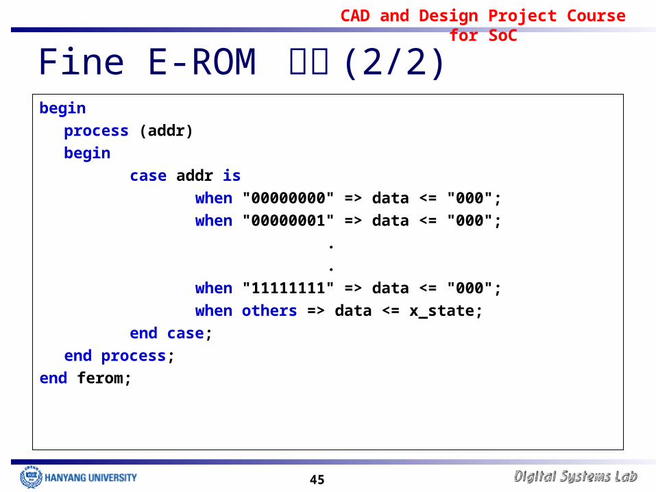
Fine E-ROM 설계 (1/2)library ieee;use ieee.std_logic_1164.all;
entity ferom isport (addr: in std_logic_vector (7 downto 0);
data: out std_logic_vector (2 downto 0));end ferom;
architecture ferom of ferom isconstant x_state: std_logic_vector := "XXX";
-- “data” is a 3-bit output data. (FE3 〜 FE1)
CAD and Design Project Course for SoC
45
Fine E-ROM 설계 (2/2)begin
process (addr)begin
case addr iswhen "00000000" => data <= "000";when "00000001" => data <= "000";
.
.when "11111111" => data <= "000";when others => data <= x_state;
end case;end process;
end ferom;
CAD and Design Project Course for SoC
46
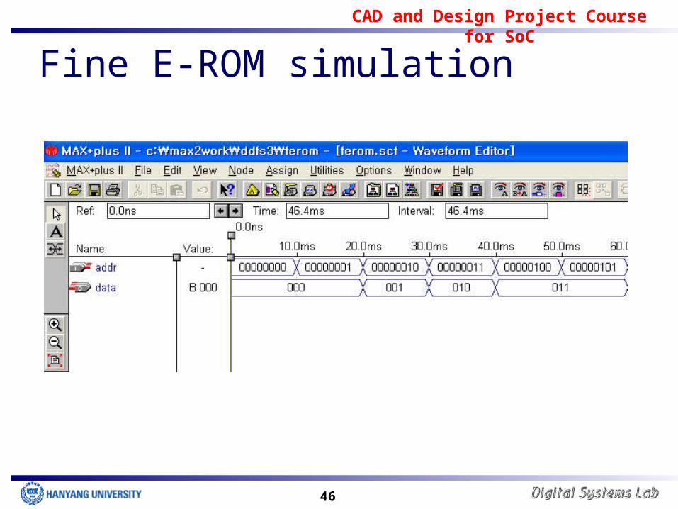
Fine E-ROM simulation
CAD and Design Project Course for SoC
47
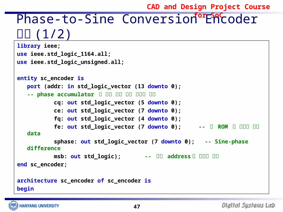
Phase-to-Sine Conversion Encoder 설계(1/2)library ieee;use ieee.std_logic_1164.all;use ieee.std_logic_unsigned.all;
entity sc_encoder isport (addr: in std_logic_vector (13 downto 0);-- phase accumulator 의 출력 값을 입력 값으로 사용 cq: out std_logic_vector (5 downto 0); ce: out std_logic_vector (7 downto 0); fq: out std_logic_vector (4 downto 0); fe: out std_logic_vector (7 downto 0); -- 각 ROM 에 들어갈 입력 data sphase: out std_logic_vector (7 downto 0); -- Sine-phase difference msb: out std_logic); -- 입력 address 의 최상위 비트
end sc_encoder;
architecture sc_encoder of sc_encoder isbegin
CAD and Design Project Course for SoC
48
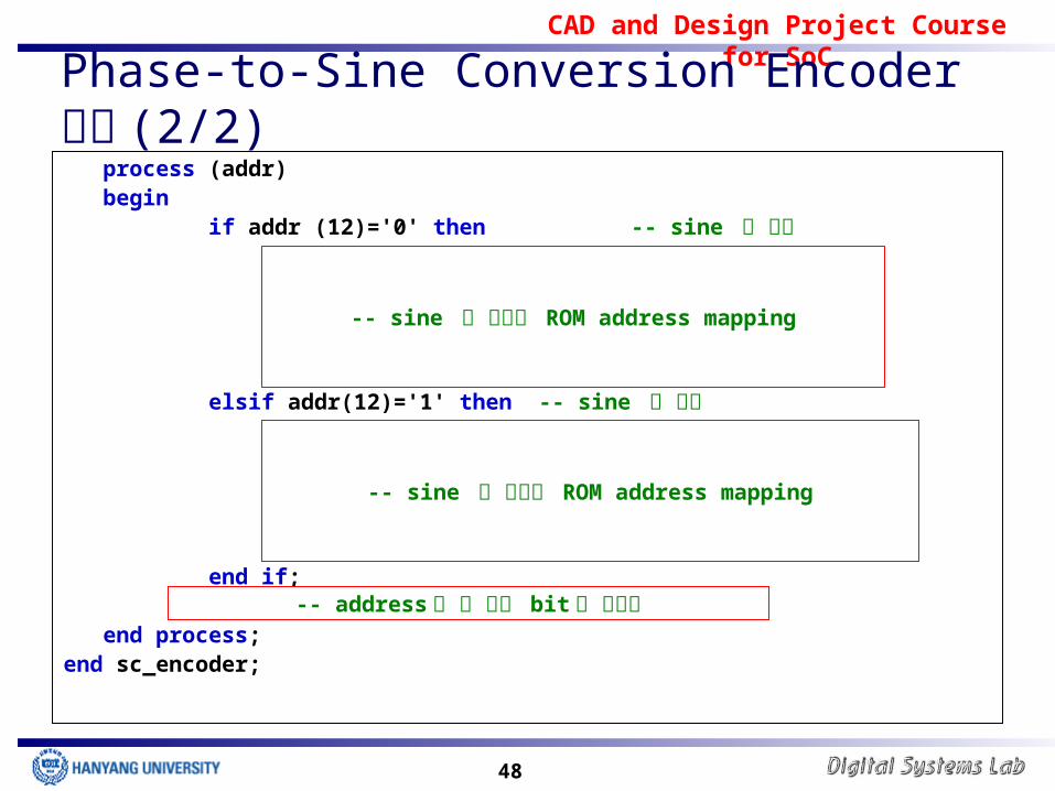
Phase-to-Sine Conversion Encoder 설계(2/2)
process (addr)begin
if addr (12)='0' then -- sine 값 증가
elsif addr(12)='1' then -- sine 값 감소
end if;
end process;end sc_encoder;
-- sine 값 증가시 ROM address mapping
-- sine 값 감소시 ROM address mapping
-- address 의 최 상위 bit 를 넘겨줌
CAD and Design Project Course for SoC
49
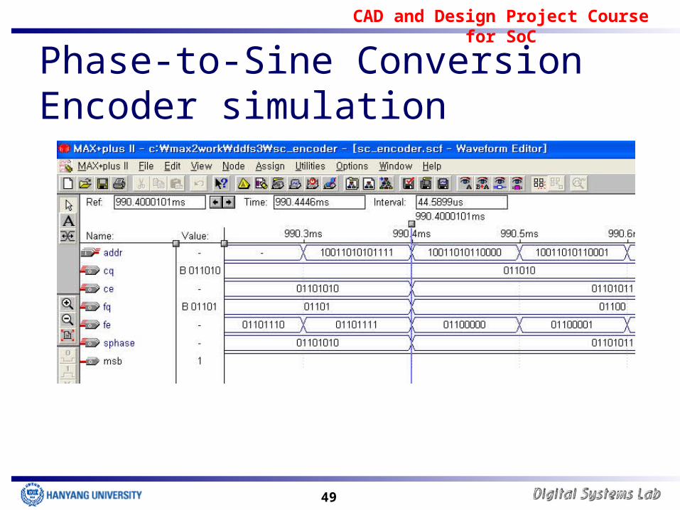
Phase-to-Sine Conversion Encoder simulation
CAD and Design Project Course for SoC
50
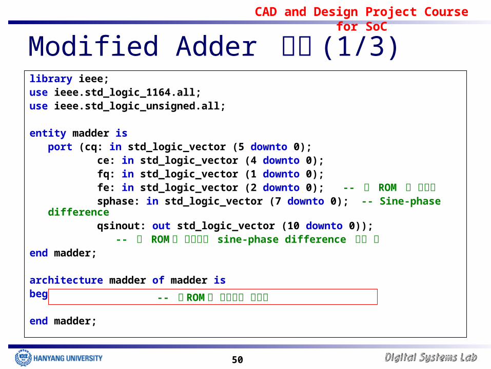
Modified Adder 설계 (1/3)library ieee;use ieee.std_logic_1164.all;use ieee.std_logic_unsigned.all;
entity madder isport (cq: in std_logic_vector (5 downto 0); ce: in std_logic_vector (4 downto 0); fq: in std_logic_vector (1 downto 0); fe: in std_logic_vector (2 downto 0); -- 각 ROM 의 출력값 sphase: in std_logic_vector (7 downto 0); -- Sine-phase difference qsinout: out std_logic_vector (10 downto 0));
-- 각 ROM 의 출력값과 sine-phase difference 값의 합end madder;
architecture madder of madder isbegin
end madder;-- 각 ROM 의 출력값을 더해줌
CAD and Design Project Course for SoC
51
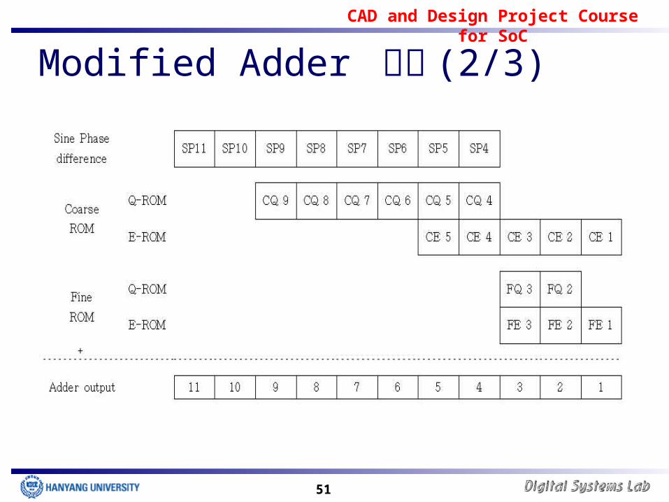
Modified Adder 설계 (2/3)
CAD and Design Project Course for SoC
52
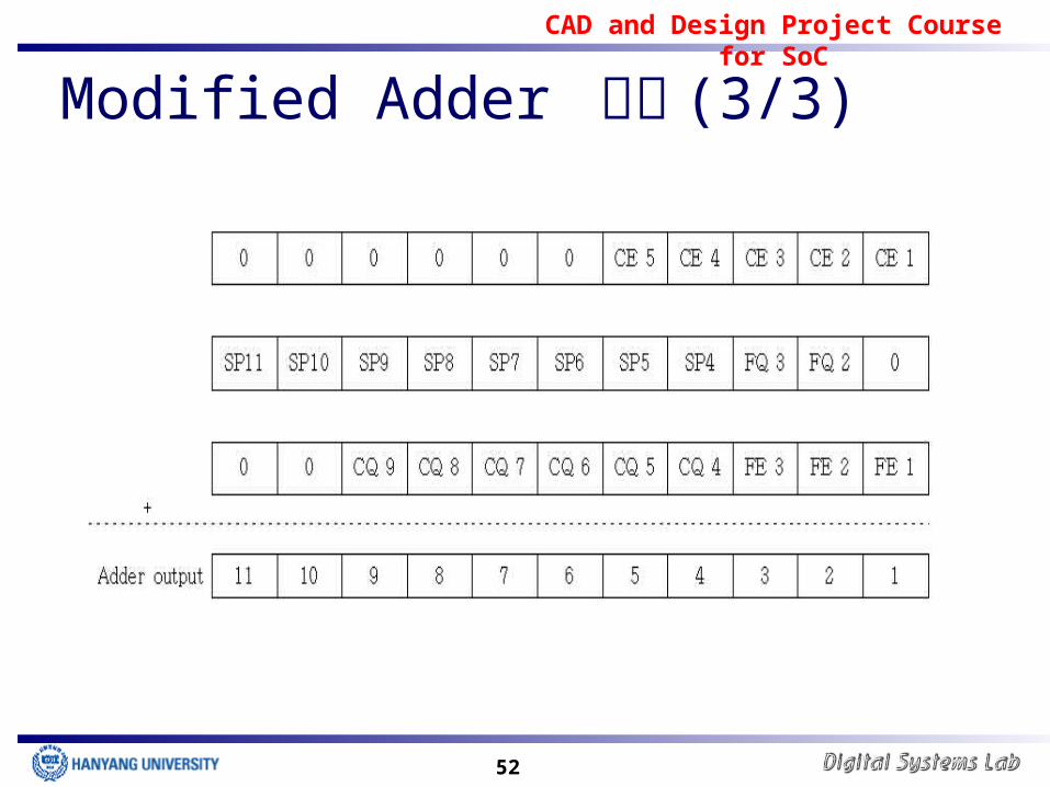
Modified Adder 설계 (3/3)
CAD and Design Project Course for SoC
53
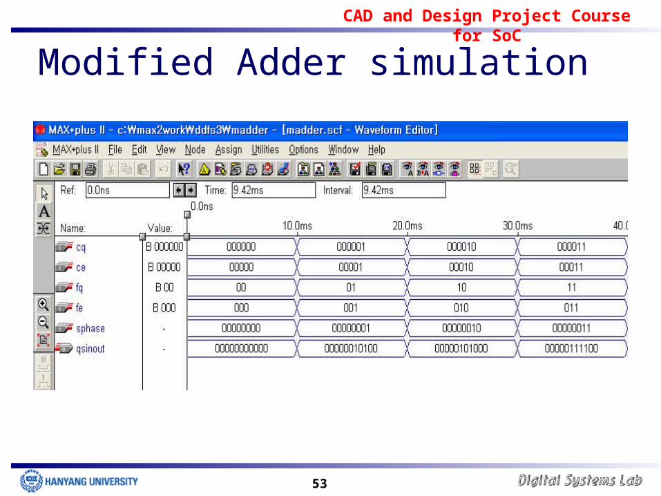
Modified Adder simulation
CAD and Design Project Course for SoC
54
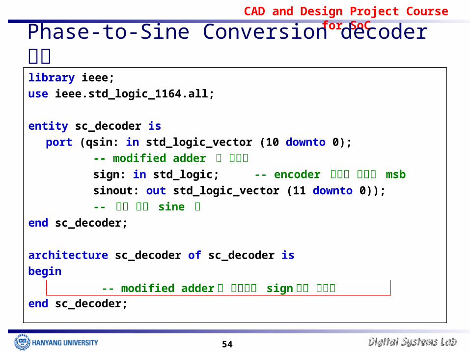
Phase-to-Sine Conversion decoder 설계 library ieee;use ieee.std_logic_1164.all;
entity sc_decoder isport (qsin: in std_logic_vector (10 downto 0);
-- modified adder 의 출력값 sign: in std_logic; -- encoder 에서의 출력된 msbsinout: out std_logic_vector (11 downto 0));-- 최종 출력 sine 값
end sc_decoder;
architecture sc_decoder of sc_decoder isbegin
end sc_decoder;-- modified adder 의 출력값에 sign 값을 더해줌
CAD and Design Project Course for SoC
55
Phase-to-Sine Conversion decoder simulation
CAD and Design Project Course for SoC
56
Sine wave generator 설계 (1/5) library ieee;use ieee.std_logic_1164.all;
entity sin_gen isport (addr: in std_logic_vector (13 downto 0); -- 14-bit 입력 address sinout: out std_logic_vector (11 downto 0)); -- 12-bit 출력 sine 값
end sin_gen;
architecture sin_gen of sin_gen is
component sc_encoder
end component;
-- component 선언
CAD and Design Project Course for SoC
57
Sine wave generator 설계 (2/5) component cqrom
end component;
component cerom
end component;
component fqrom
end component;
component ferom
end component;
-- component 선언
-- component 선언
-- component 선언
-- component 선언
CAD and Design Project Course for SoC
58
Sine wave generator 설계 (3/5) component madder
end component;
component sc_decoder
end component;
-- component 선언
-- component 선언
CAD and Design Project Course for SoC
59
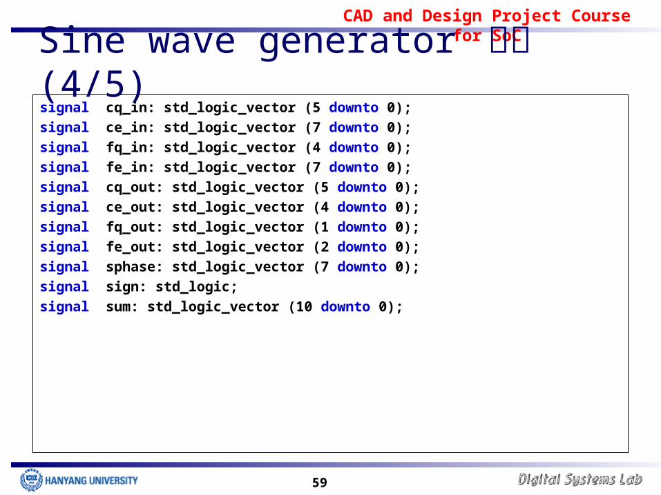
Sine wave generator 설계 (4/5) signal cq_in: std_logic_vector (5 downto 0);signal ce_in: std_logic_vector (7 downto 0);signal fq_in: std_logic_vector (4 downto 0);signal fe_in: std_logic_vector (7 downto 0);signal cq_out: std_logic_vector (5 downto 0);signal ce_out: std_logic_vector (4 downto 0);signal fq_out: std_logic_vector (1 downto 0);signal fe_out: std_logic_vector (2 downto 0);signal sphase: std_logic_vector (7 downto 0);signal sign: std_logic;signal sum: std_logic_vector (10 downto 0);
CAD and Design Project Course for SoC
60
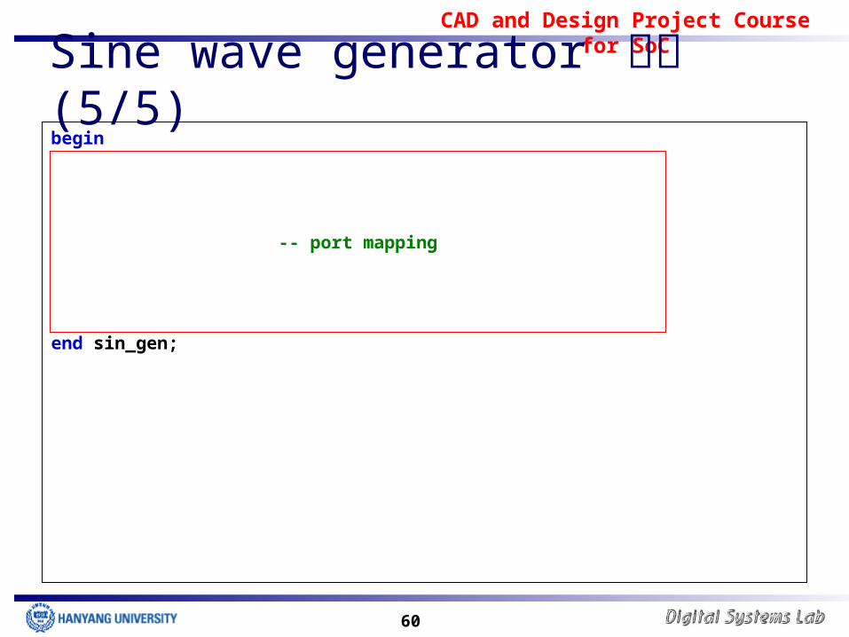
Sine wave generator 설계 (5/5) begin
end sin_gen;
-- port mapping
CAD and Design Project Course for SoC
61
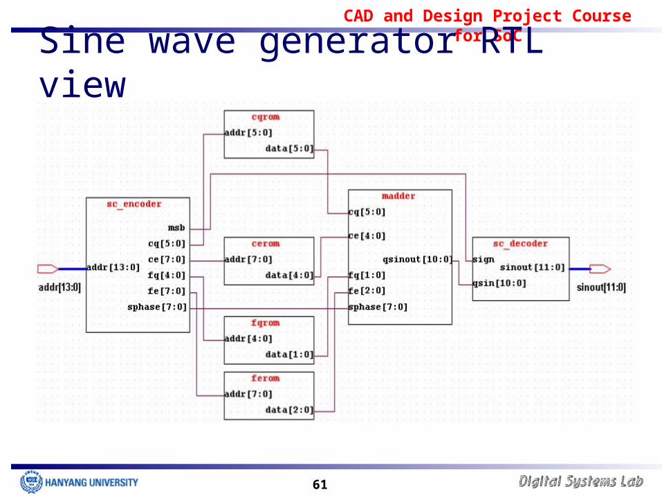
Sine wave generator RTL view
CAD and Design Project Course for SoC
62
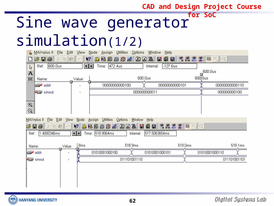
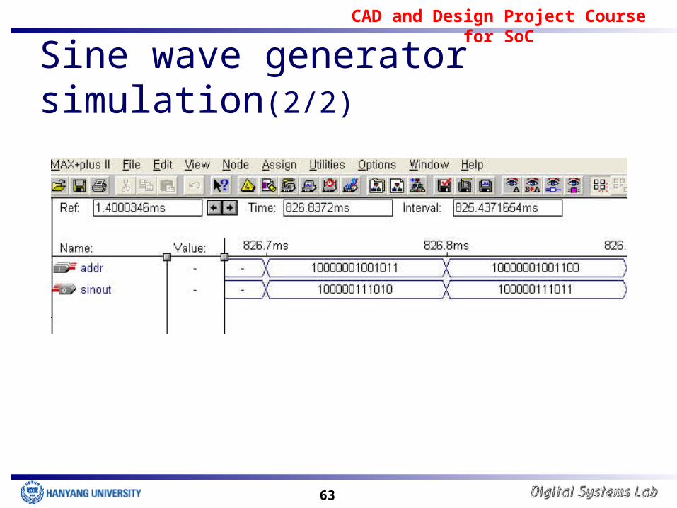
Sine wave generator simulation(1/2)
CAD and Design Project Course for SoC
63
Sine wave generator simulation(2/2)
CAD and Design Project Course for SoC
64
DDFS 설계 (1/2) library ieee;use ieee.std_logic_1164.all;
entity ddfs isport (fcw: in std_logic_vector (13 downto 0); reset, sclk: in std_logic; sinout: out std_logic_vector (11 downto 0));
end ddfs;-- 14-bit frequency control word 를 입력값으로 받아서-- 12-bit sine data 를 출력architecture behave of ddfs is
component phase_accumulator
end component;
-- port 선언
CAD and Design Project Course for SoC
65
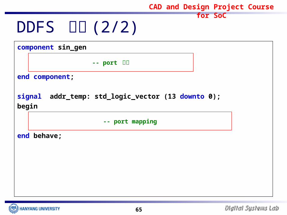
DDFS 설계 (2/2) component sin_gen
end component;
signal addr_temp: std_logic_vector (13 downto 0);begin
end behave;
-- port 선언
-- port mapping

CAD and Design Project Course for SoC
66
DDFS RTL view
CAD and Design Project Course for SoC
67
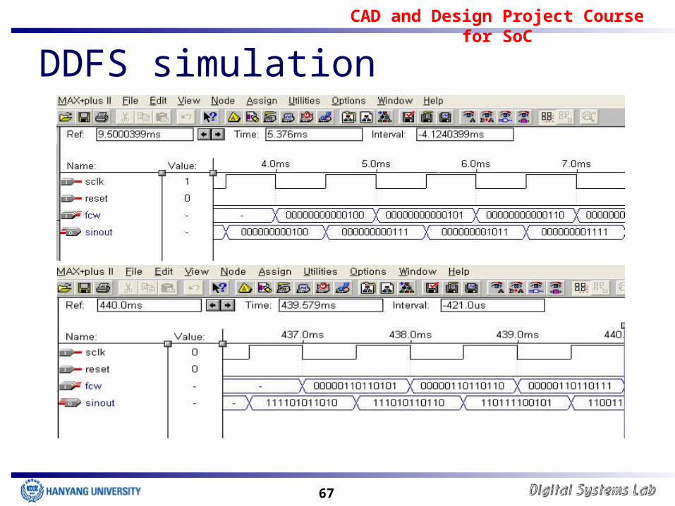
DDFS simulation
CAD and Design Project Course for SoC
68
참고문헌 Jinchoul Lee, Hyunchul Shin, "New Effective ROM
Compression Methods for ROM-based Direct Digital Frequency Synthesizer Design“, IEICE Trans. Communications, Nov. 2004 , pp.3352-3355
이진철 , 신현철 , "New ROM Compression Methods for Direct Digital Frequency Synthesizers", 2002 SOC Design Conference 학술대회 눈문집 , Oct. 2002
J.Tierney,C.M. Rader, and B. Gold, "A digital frequency synthesizer", IEEE Trans. Audio Electroacoustic, vol. AU-19,
pp. 48-56, mar. 1971. David A Sunderland, et al., "CMOS/SOS Frequency
Synthesizer LSI Circuit for Spread Spectrum Communications", IEEE J. Solid-State Circuits, vol. 19, no. 4, pp. 497-505, Aug. 1984.
ByungDo Yang, KiHyuk Sung, YoungJoon Kim, Lee-Sup Kim, Seon-Ho Han, and HyunKyu Yoo, “A Direct Digital Frequency Synthesizer Using A New ROM Compression Method”, European Solid-State Circuit Conference 2001, Sep. 2001.
L.A. Weaver, 'High Resolution Phase to Sine Amplitude Conversion',U.S. Patent 4 905 177, Feb. 1990.
Minkyoung PARK, "CORDIC-Based Direct Digital Frequency Synthesizer : Comparison with a ROM-Based Architecture in FPGA Implementation", IEICE Trans. FUNDAMENTAL, Vol. E83-A, No. 6, pp. 1282-1285, June 2000.