Embed Size (px)
Citation preview
8/3/2019 ht2860
http://slidepdf.com/reader/full/ht2860 1/9
HT2860
6-Sound Generator
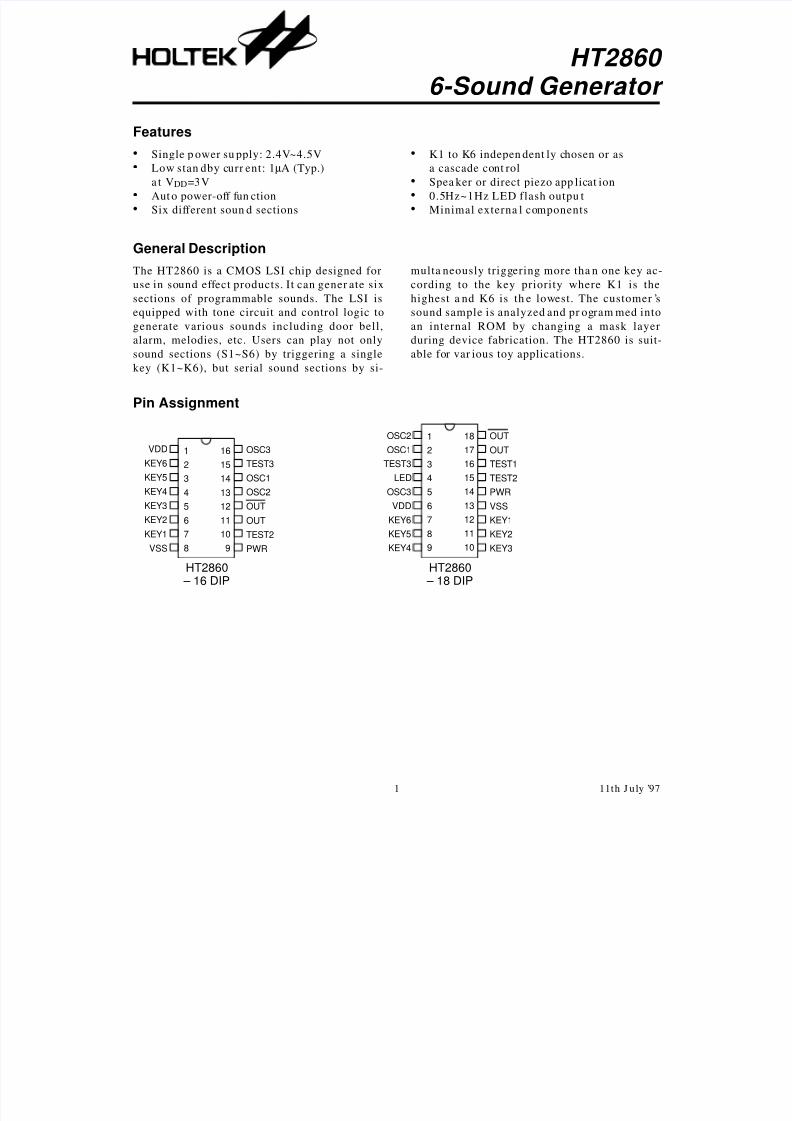
Pin Assignment
General Description
The HT2860 is a CMOS LSI chip designed for
use in sound effect products. It can gener ate six
sections of programmable sounds. The LSI is
equipped with tone circuit and control logic to
generate various sounds including door bell,
alarm, melodies, etc. Users can play not only
sound sections (S1~S6) by triggering a single
key (K1~K6), but serial sound sections by si-
multa neously triggering more tha n one key ac-
cording to the key priority where K1 is the
highest a nd K6 is th e lowest. The customer ’s
sound sample is analyzed and pr ogram med into
an internal ROM by changing a mask layer
during device fabrication. The HT2860 is suit-
able for var ious toy applications.
Features
• Single p ower su pply: 2.4V~4.5V• Low stan dby curr ent: 1µA (Typ.)
a t VDD=3V
• Aut o power-off fun ction• Six different soun d sections
• K1 to K6 indepen dent ly chosen or as
a cascade cont rol• Spea ker or direct piezo app licat ion
• 0.5Hz~1Hz LED flash outpu t• Minimal externa l components
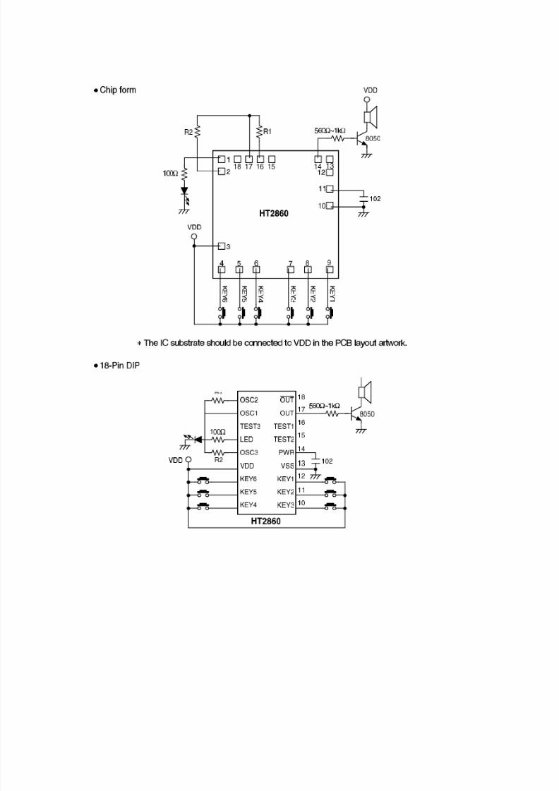
HT2860
– 18 DIP
18
17
16
15
14
13
12
11
10
1
2
3
4
5
6
7
8
9
OUT
OUT
TEST1
TEST2
PWR
VSS
KEY1
KEY2
KEY3
VDD
KEY6
KEY5
KEY4
KEY3
KEY2
KEY1
VSS
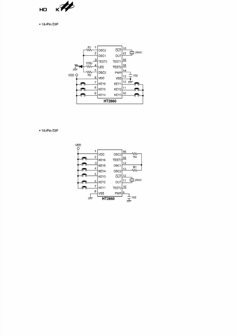
HT2860
– 16 DIP
OSC3
TEST3
OSC1
OSC2
OUT
OUT
TEST2
PWR
16
15
14
13
12
11
10
9
1
2
3
4
5
6
7
8
OSC2
OSC1
TEST3
LED
OSC3
VDD
KEY6
KEY5
KEY4
1 11th J uly ’97
8/3/2019 ht2860
http://slidepdf.com/reader/full/ht2860 2/9
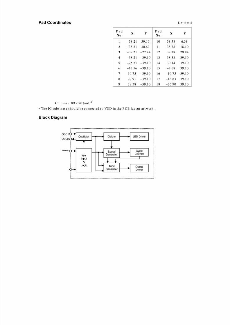
Pad Coordinates Unit: mil
P ad
No.X Y
P ad
No.X Y
1 –38.21 39.10 10 38.38 6.38
2 –38.21 30.60 11 38.38 18.10
3 –38.21 –22.44 12 38.38 29.84
4 –38.21 –39.10 13 38.38 39.10
5 –25.71 –39.10 14 30.14 39.10
6 –13.56 –39.10 15 –2.68 39.10
7 10.75 –39.10 16 –10.75 39.10
8 22.91 –39.10 17 –18.83 39.10
9 38.38 –39.10 18 –26.90 39.10
Chip size: 89 × 90 (mil)2
∗ The IC substr at e should be connected t o VDD in the P CB layout art work.
Block Diagram
8/3/2019 ht2860
http://slidepdf.com/reader/full/ht2860 3/9
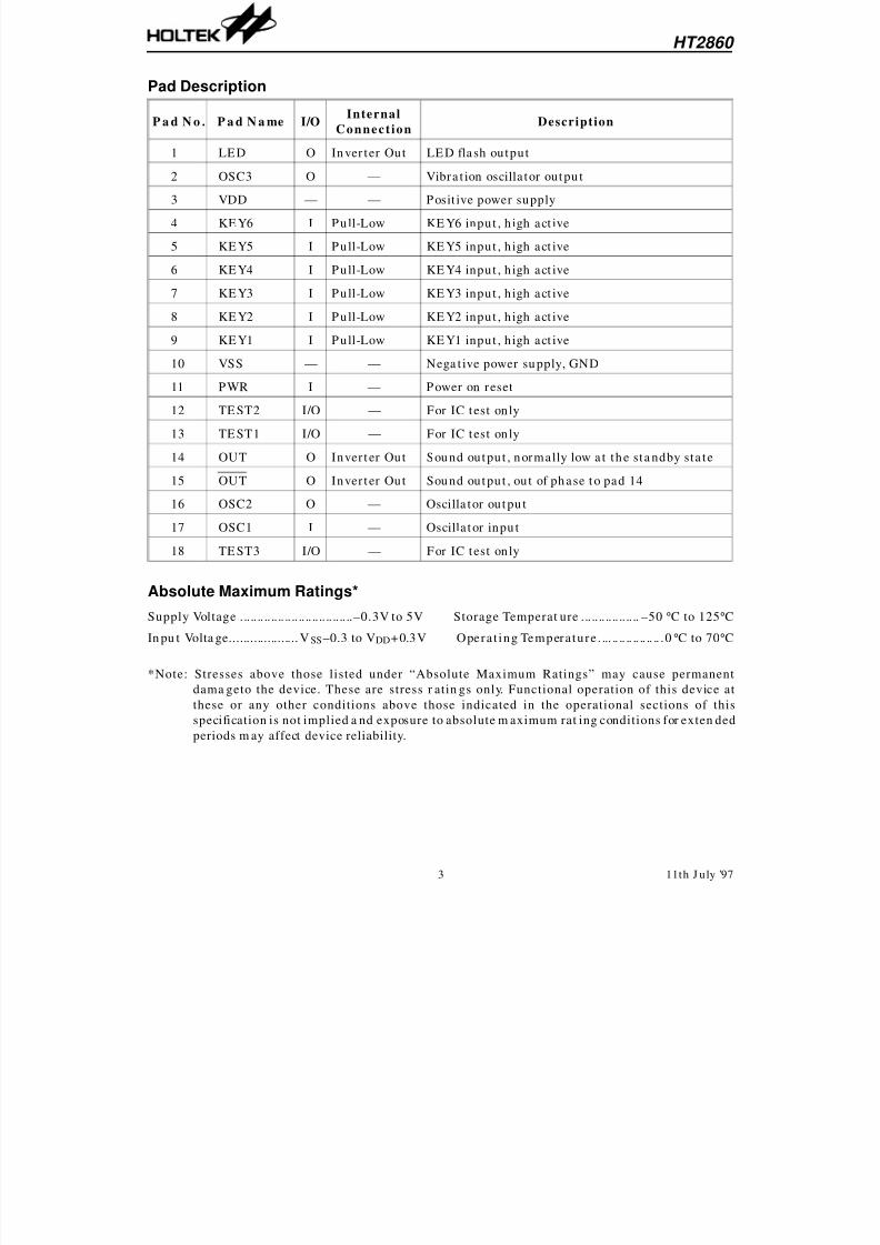
Pad Description
P a d N o . P a d N a me I/OInternal
ConnectionDescription
1 LED O Inver ter Out LED flash output
2 OSC3 O — Vibra t ion oscilla tor outpu t
3 VDD — — Posit ive power supply
4 KEY6 I Pull-Low KE Y6 input , h igh act ive
5 KEY5 I Pull-Low KE Y5 input , h igh act ive
6 KEY4 I Pull-Low KE Y4 input , h igh act ive
7 KEY3 I Pull-Low KE Y3 input , h igh act ive
8 KEY2 I Pull-Low KE Y2 input , h igh act ive
9 KEY1 I Pull-Low KE Y1 input , h igh act ive
10 VSS — — Nega tive power supply, GND
11 PWR I — Power on reset
12 TEST2 I/O — For IC test only
13 TEST1 I/O — For IC test only
14 OUT O Inver ter Out Sound output , normally low a t the sta ndby sta te
15 OUT O Inver ter Out Sound output , out of phase to pad 14
16 OSC2 O — Oscilla tor outpu t
17 OSC1 I — Oscilla tor inpu t
18 TEST3 I/O — For IC test only
Absolute Maximum Ratings*
Supply Voltage ... .. .. .. .. .. .. .. .. .. .. .. .. .. .. ..–0.3V to 5V Storage Temperat ure ... .. .. .. .. .. .. .. –50°C to 125°C
In pu t Volta ge.................... VSS–0.3 to VDD+0.3V Operat ing Temperature . ... .. .. .. .. .. .. .. . 0°C to 70°C
*Note: Stresses above those listed under “Absolute Maximum Ratings” may cause permanent
dama geto the device. These are stress r atin gs only. Functional operation of this device at
these or any other conditions above those indicated in the operational sections of this
specification is not implied a nd exposure to absolute m aximum rat ing conditions for exten ded
periods m ay affect device reliability.
HT2860
3 11th J uly ’97
8/3/2019 ht2860
http://slidepdf.com/reader/full/ht2860 4/9
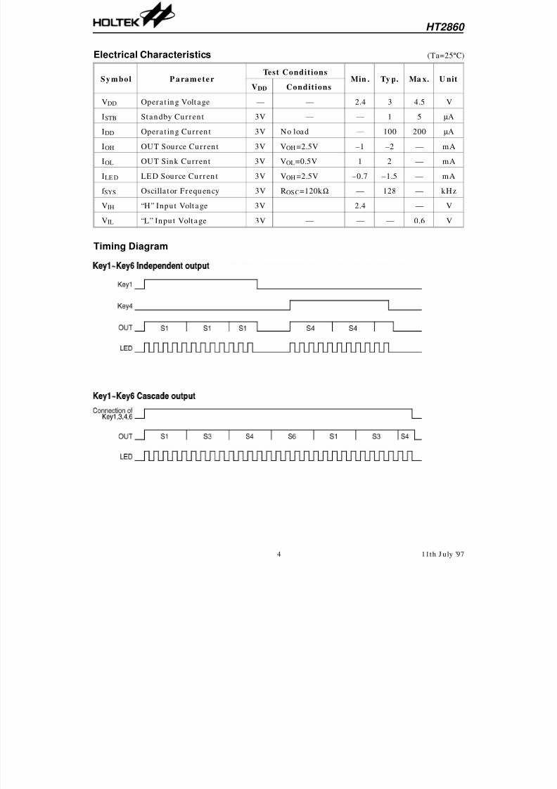
Electrical Characteristics (Ta=25°C)
Symbol P aram e te rTest Conditions
Min . Ty p. Ma x. U nitVDD Conditions
VDD Opera t ing Voltage — — 2.4 3 4.5 V
ISTB Standby Current 3V — — 1 5 µA
IDD Opera t ing Curren t 3V No load — 100 200 µA
IOH OUT Source Curren t 3V VOH =2.5V –1 –2 — mA
IOL OUT Sink Current 3V VOL=0.5V 1 2 — mA
ILE D LED Source Curren t 3V VOH =2.5V –0.7 –1.5 — mA
f SYS Oscilla tor Frequency 3V ROS C=120k Ω — 128 — kHz
VIH “H” Input Voltage 3V — 2.4 — — V
VIL “L” Inpu t Voltage 3V — — — 0.6 V
Timing Diagram
HT2860
4 11th J uly ’97
8/3/2019 ht2860
http://slidepdf.com/reader/full/ht2860 5/9

8/3/2019 ht2860
http://slidepdf.com/reader/full/ht2860 6/9
8/3/2019 ht2860
http://slidepdf.com/reader/full/ht2860 7/9

8/3/2019 ht2860
http://slidepdf.com/reader/full/ht2860 8/9
8/3/2019 ht2860
http://slidepdf.com/reader/full/ht2860 9/9
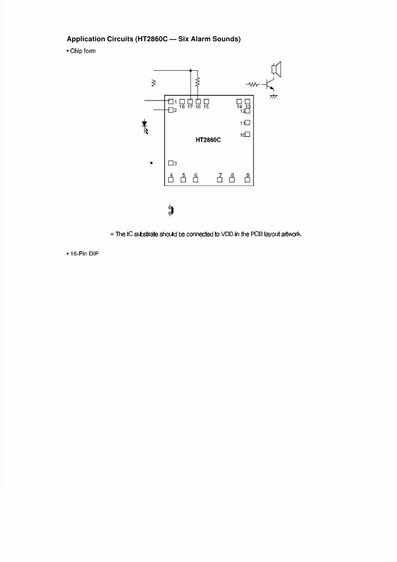
Application Circuits (HT2860C — Six Alarm Sounds)


