Embed Size (px)
Citation preview

Satellite Computer System based on LEON Technology –
Mid Semester Presentation
סמסטר חורף תשס"ח 9/1/2008
פרויקט דו-סמסטריאלי
Ira Joffe & Yossi Zadik
Supervised by: Ina Rivkin

Table of Contents
Project Goals The Leon3 System Block Diagram (Part A) The AMBA Bus Hardware Overview Software Overview Project Road Map

Project Goals – Part A
Leon 3 environment study:– Hardware structure– Software structure– Tools: introduction and usage
Implementation – basic Leon system with small user core :– Software & HW coding– Implementation on RASTA board

Block Diagram - System Part A
SPARC V8 32-bit processor
AMBA bus – AHB, APB
Memory controller – ROM, SRAM, SDRAM
JTAG Interface Debug unit – access
to the processor

THE AMBA BUS
Overview
AMBA BUS – OVERVIEW
AHB System APB Connector

AMBA BUS MAIN COMPONENETS
AHB MASTER – Initiates read and write operations by providing the address and the control information. Only one is active at a time.
AHB SLAVE – Responds to the r/w operations initiated by the master and signals back the success, failure or waiting of the data transfer.
AHB ARBITER – Ensures that only one bus master at a time is allowed to initiate data transfers. Any arbitration algorithm can be implemented.
AHB DECODER – decodes the address of each transfer and provide a select signal for the slave involved.
APB bridge - connector to a lower bandwidth APB bus where most of the peripherals are located.

Core I/F with AMBA Bus
HARDWARE CONFIGURATION & MODULATION
XCONFIG & XGRLIB GUIs

Hardware Introduction – Available IP’s
IP cores are given by Gaisler’s GRLIB May be added according to user needs (and
license) Our own User Core may be added Includes : protocols, connections, I/O, etc. Example : Can, SpaceWire, Ethernet, UART,
VGA output, PCI, PS/2

XCONFIG – HW configuration GUIexample – enabling 2nd UART

XCONFIG - outputs
Terminal prints – config file changes
.config file output
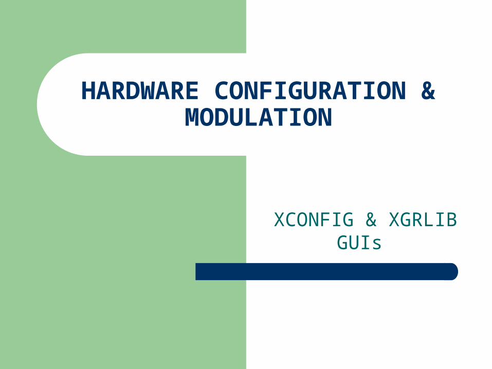
XCONFIG – implementation in VHDL code
Leon3mp.vhd VHDL code – where config file influences code
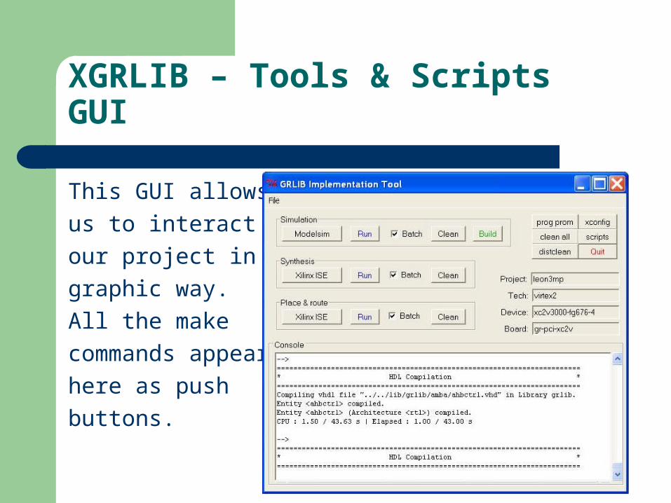
XGRLIB – Tools & Scripts GUI
This GUI allows
us to interact with
our project in a
graphic way.
All the make
commands appear
here as push
buttons.

USER IP CORE GENERATION
Adding our own
AHB slave (AND Unit)

IP Core Generation
We Wish to add a new IP core to the system. One that will do a very simple function – AND between 2 signals and provide the result. For that we will do the following steps:
1. Write the VHDL code2. Connect our IP to the LEON3MP system through
the AHB Bus3. Write a C code that demonstrates our IP
functionality4. Run simulation and check result

Connecting the IP – Definition & Instantiation
Leon3mp.vhd file
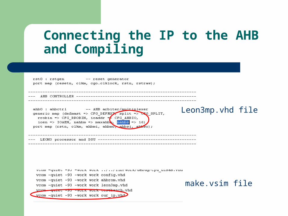
Connecting the IP to the AHB and Compiling
Leon3mp.vhd file
make.vsim file

Writing the C Code
int our_ip_test (){ int *num1; int *num2; int i; num1 = (int*)0xb0000004; num2 = (int*)0xb0000008;
*num1 = 0x11111000; *num2 = 0x00001111;
i = *(int*)0xb0000000; return i;
}

Running the Simulation

SOFTWARE
Programming the Leon3
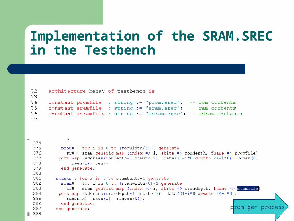
Implementation of the SRAM.SREC in the Testbench
prom gen process

System Interaction
We wish to write a program to the Leon3 system and see that the signals run according to it and with the parameters of our program. We’ll go through the process of:
Writing the C program Compile and generate the SREC file Replace the existing SRAM.SREC file with our own Run simulation and check outcome

Step 1 – Writing the C Program
our_test () {
int i;
int *Array = 0x40005000;
for (i=0;i<32;i++) {
Array[i] = i;
}
}
We wrote a very simple
program:
Creating an array at a fixed location in the memory (middle of the SRAM). It’s size is 32 int, and contains the int 0-31.

Step 2 – Compile and Generate the SREC File
We generated the SREC file using these following commands:
Sparc-elf-gcc –g –O2 our_test.c -S -o our_test.s Sparc-elf-as –g our_test.s -o our_test.o Sparc-elf-objcopy –O srec our_test.o sram.SREC
..And got the new sram.SREC file.
C -> srec view

Step 3 – The new SREC File
S00C00007372616D2E7372656365
S315400000009DE3BF9003100014C227BFF0C027BFF482
S31540000010C207BFF480A0601F1480000D01000000DD
S31540000020C207BFF4BB286002C207BFF0BA0740014F
S31540000030C207BFF4C2274000C207BFF48200600176
S31540000040C227BFF410BFFFF301000000B01000014B
S3154000005081C7E00881E800000000000000000000C1
S31540000060000000000000000000000000000000004A
S70540000000BA
Address
Op. Code
Opcode read on wave

Step 4 – Simulation:Op. Code Execution
Wave explanation

Project Road Map – Part A
Leon 3 system study – HW, SW, Tools Creating Work Environment Software generation process
– Coding– SRAM generation
Hardware generation process:– Writing a user core– Connection to the AMBA I/F– Debugging
Implementation on FPGA: DD– Synthesis and Place & Route 15.1.08– HW Debugging – UART, Chipscope 23.1.08– SW Debugging 30.1.08

The End

PROM GENERATION
prom.S prom.o
prom.exe prom.SREC
gcc - compile
gcc - linker Objcopy – binary to hex

S00C000070726F6D2E737265635AS113000081D8200003000004821060E08188400051S113001081900000819800008180000001000000B0S1130020030020408210600FC2A0004087444000BBS11300308608E01F881000008A1000008C10000061S11300408E100000A0100000A2100000A4100000F8S1130050A6100000A8100000AA100000AC100000B8S1130060AE100000901000009210000094100000E8S113007096100000981000009A1000009C100000D8S11300809E10000086A0E00116BFFFEF81E0000093S1130090821020028190400003000004821060E07ES11300A08188400001000000010000000100000000S11300B0874440008730E01C8688E00F12800016D9S11300C00320000005040E008410A233C420400065S11300D00539A81B8410A260C4206004050003FC39S11300E0C420600882103860C40040008530A00C31S11300F0030000048210600980A040021280000600S1130100033FFC00821061000539A81B8410A26023S1130110C4204000050000088210000080A0E00018S113012002800005010000008200400210BFFFFCB5S11301308620E0013D1003FFBC17A3E0BC2780012BS11301409C27A0600310000081C040000100000053S11301500100000001000000010000000100000097S1130160000000000000000000000000000000008BS9030000FC
Start code, one character, an ASCII letter 'S'.
Record type, one digit, 0 to 9, defining the type of the data field.
Byte count, two hex digits, a number of bytes (hex digit pairs) in the address, data and checksum fields.
Address, four, six or eight hex digits, the memory position for the data. This address is big endian.
Data, a sequence of n bytes of the data themselves. 2n hex digits.
Checksum, two hex digits. One’s component of the LSB.
The SREC File

Wave Diagram

PROGRAM GENERATION IN OUR PROJECT
The PROM does several initializations – registers, interrupts, traps, instruction and frame pointers.
After this stage the PROM jumps to the SRAM start. It is easier to enter the program to the SRAM and keep the
default initial settings. The SRAM.SREC file is created from the system.C file which
calls on different functions from Software/Leon3. The stages for SRAM generation are almost the same as
PROM, except Gaisler gives us a tool – BCC (Blind Cross Compiler) which enables us to do the following process:sram.c -> sram.o -> sram.srec
back

C to Assembler to SREC
1:our_test.c .LLM1:0000 9DE3BF90 save %sp, -112, %sp our_test () {0004 03100014 sethi %hi(1073762304), %g1 int *Array = (int *)0x40005000;0008 C227BFF0 st %g1, [%fp-16] .LLM3:000c C027BFF4 st %g0, [%fp-12] int i; .LL2:0010 C207BFF4 ld [%fp-12], %g1 for (i=0;i<32;i++) { 0014 80A0601F cmp %g1, 310018 1480000D bg .LL3001c 01000000 nop .LLM5:0020 C207BFF4 ld [%fp-12], %g1 Array[i] = i;0024 BB286002 sll %g1, 2, %i50028 C207BFF0 ld [%fp-16], %g1002c BA074001 add %i5, %g1, %i50030 C207BFF4 ld [%fp-12], %g10034 C2274000 st %g1, [%i5]0038 C207BFF4 ld [%fp-12], %g1003c 82006001 add %g1, 1, %g10040 C227BFF4 st %g1, [%fp-12]0044 10BFFFF3 b .LL2 };0048 01000000 nop .LL3: };004c B0100001 mov %g1, %i00050 81C7E008 ret0054 81E80000 restore Back

Step 4 – Simulation:Reading the Op. Code
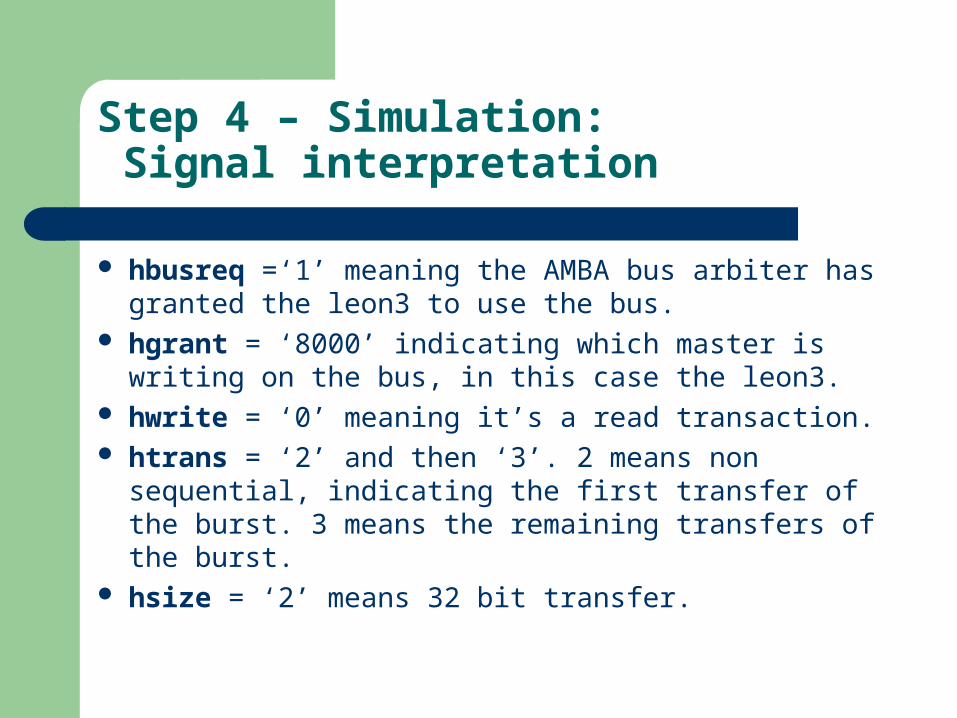
Step 4 – Simulation:Signal interpretation
hbusreq =‘1’ meaning the AMBA bus arbiter has granted the leon3 to use the bus.
hgrant = ‘8000’ indicating which master is writing on the bus, in this case the leon3.
hwrite = ‘0’ meaning it’s a read transaction. htrans = ‘2’ and then ‘3’. 2 means non sequential,
indicating the first transfer of the burst. 3 means the remaining transfers of the burst.
hsize = ‘2’ means 32 bit transfer.

Step 4 – Simulation:Signal interpretation
hburst = ‘1’ meaning incrementing burst of unspecified length. haddr = ‘40000000’ is the first address we saw in the SREC file
which will contain the first op. code. The addresses which follow advance by +4.
hready goes up every time the op. code of the address requested has been fetched and is ready for reading.
hdata = ‘9DE3BF90’ shows the op. code from a given address. The first one is showed in the SREC file.
hsel = ‘8000’ indicating to which slave the bus addresses, in this case the memory controller.
Back
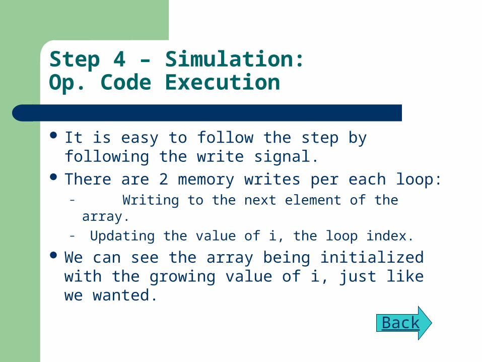
Step 4 – Simulation:Op. Code Execution
It is easy to follow the step by following the write signal.
There are 2 memory writes per each loop:– Writing to the next element of the array.– Updating the value of i, the loop index.
We can see the array being initialized with the growing value of i, just like we wanted.
Back