Embed Size (px)
Citation preview
Studying Electrostatic Polarization Forces at the
Nanoscale
Dielectric constant of supported biomembranes measured in air and liquid
environment
Georg Gramse
ADVERTIMENT. La consulta d’aquesta tesi queda condicionada a l’acceptació de les següents condicions d'ús: La difusió d’aquesta tesi per mitjà del servei TDX (www.tdx.cat) ha estat autoritzada pels titulars dels drets de propietat intel·lectual únicament per a usos privats emmarcats en activitats d’investigació i docència. No s’autoritza la seva reproducció amb finalitats de lucre ni la seva difusió i posada a disposició des d’un lloc aliè al servei TDX. No s’autoritza la presentació del seu contingut en una finestra o marc aliè a TDX (framing). Aquesta reserva de drets afecta tant al resum de presentació de la tesi com als seus continguts. En la utilització o cita de parts de la tesi és obligat indicar el nom de la persona autora. ADVERTENCIA. La consulta de esta tesis queda condicionada a la aceptación de las siguientes condiciones de uso: La difusión de esta tesis por medio del servicio TDR (www.tdx.cat) ha sido autorizada por los titulares de los derechos de propiedad intelectual únicamente para usos privados enmarcados en actividades de investigación y docencia. No se autoriza su reproducción con finalidades de lucro ni su difusión y puesta a disposición desde un sitio ajeno al servicio TDR. No se autoriza la presentación de su contenido en una ventana o marco ajeno a TDR (framing). Esta reserva de derechos afecta tanto al resumen de presentación de la tesis como a sus contenidos. En la utilización o cita de partes de la tesis es obligado indicar el nombre de la persona autora. WARNING. On having consulted this thesis you’re accepting the following use conditions: Spreading this thesis by the TDX (www.tdx.cat) service has been authorized by the titular of the intellectual property rights only for private uses placed in investigation and teaching activities. Reproduction with lucrative aims is not authorized neither its spreading and availability from a site foreign to the TDX service. Introducing its content in a window or frame foreign to the TDX service is not authorized (framing). This rights affect to the presentation summary of the thesis as well as to its contents. In the using or citation of parts of the thesis it’s obliged to indicate the name of the author.
Studying Electrostatic
Polarization Forces at the
Nanoscale
Dielectric constant of supported
biomembranes measured in air and liquid
environment
Georg Gramse
Barcelona, May 2012
DOCTORAL THESIS

UNIVERSIDAD DE BARCELONA
Facultad de Física
Departamento de Electrónica
Estudios de Fuerzas de
Polarización Electrostática
a la Nanoescala La constante dieléctrica de biomembranas
suportadas medido en aire y liquido
Programa de Doctorado:
Nanociencias
Línea de Investigación:
Nanobiotecnología
Director de Tesis:
Gabriel Gomila Lluch
Autor:
Georg Gramse

Contents
1 INTRODUCTION 1
2 ELECTRICAL ATOMIC FORCE
MICROSCOPY TECHNIQUES 5
2.1 Scanning Probe Microscopy & Atomic Force Microscopy 5
2.1.1 AFM Topography scanning modes 8
2.2 Atomic force microscopy techniques for electrical characterization 14
2.2.1 Conductive Atomic Force Microscopy 15
2.2.2 Scanning Capacitance Microscopy (SCM) 16
2.2.3 Nanoscale Impedance Microscopy (NIM) 17
2.2.4 Scanning Microwave Microscopy (SMM) 20
2.2.5 DC-Electrostatic Force Microscopy (DC-EFM) 22
2.2.6 Amplitude Modulation Electrostatic Force Microscopy (AM-EFM) 23
2.2.7 Frequency Modulation Electrostatic Force Microscopy (FM-EFM) 25
2.2.8 Kelvin Probe Force Microscopy (KPFM) 27
2.2.9 Scanning Polarization Force Microscopy (SPFM) 28
2.2.10 AFM techniques for electrical characterization in liquid 30
2.2.11 Electrostatic Force Microscopy in liquid 34
2.3 Quantitative dielectric material properties
from electrical AFM-based techniques. 36
2.4 Motivation and Objectives of this work 40
3 QUANTITATIVE ELECTROSTATIC
FORCE MICROSCOPY 43
3.1 Analytical approximations of the probe-substrate force 44
3.2 Finite Element Method (FEM): Introduction into
electrostatic modeling with Comsol Multiphysics™ 47
3.2.1 A ready tool for standardized electric tip
calibration using finite element simulations 51
4 QUANTITATIVE DIELECTRIC CONSTANT
MEASUREMENT OF SUPPORTED
BIOMEMBRANES BY DC-EFM 55
4.1 Abstract 55
4.2 Introduction 56
4.3 Theoretical model and measurement protocol 58
4.4 Validation of the method 62
4.4.1 Nanoscale dielectric constant measurement on a thin SiO2 film 63
4.4.2 Nanoscale dielectric constant measurement of purple membrane 65
4.5 Discussion 69
4.6 Conclusion 74
4.7 Appendix 75
4.7.1 Parameter calibration 75
4.7.2 Statistical analysis of the data 77
4.7.3 Analytical formula for the electrostatic force on
small AFM-tips including the cone contribution 78
5 QUANTIFYING THE DIELECTRIC CONSTANT
OF THICK INSULATORS USING EFM 81
5.1 Abstract 81
5.2 Introduction 82
5.3 Theoretic modeling 83
5.4 Effects of the microscopic probe geometry on
the local electrostatic interaction 86
5.4.1 Metallic substrates 86
5.4.2 Thick insulating substrates 89
5.5 Quantification of the dielectric constant of thick insulators 92
5.6 Locality of the electrostatic force signal 100
5.7 Conclusion 103
6 DIELECTRIC CONSTANT OF BIOMEMBRANES
IN ELECTROLYTE SOLUTIONS 105
6.1 Abstract 105
6.2 Introduction 106
6.3 Experimental set up 107
6.4 Theory of electrostatic force in liquid 109
6.5 Materials and methods 110
6.6 Results 111
6.7 Discussion 118
6.8 Conclusion 119
6.9 Appendix 120
6.9.1 Dependency of electric force on voltage drop in
solution Vsol and sample dielectric constant εr 120
6.9.2 Data interpretation using finite element simulations 125
6.9.3 Calculating forces: parallel plate model
versus cone model simulations 127
7 CONCLUSION AND SUMMARY 131
7.1 Conclusions 131
7.2 Perspectives 133
7.3 Summary/Resumen (en Castellano) 135
8 APPENDIX 141
8.1 Acronyms 141
8.2 Publications 142
8.3 Acknowledgements 143
8.4 References 144

1 Introduction
Scientific progress was long confined to its subject areas, but at least since
ground braking inventions and discoveries like the double helix model by
Watson and Crick it got obvious that interdisciplinarity can often be the key to
access still unexplored fields of science. Nanotechnology or Nanoscience is one
of the big examples for interdisciplinary fields, since in principle it does not
mean anything more specific than science of very tiny things including all the
areas from Physics over Chemistry to Biology. I believe to be more
interdisciplinary is almost impossible. In a more critical way one might also say
that a vaguer definition is impossible. But actually when looking for example at
the number of scanning probe techniques for nanoscale characterization that
were developed in last 30 years and since then had great impact on science,
one finds also that nowadays most of them can be applied to investigate very
diverse problems reaching from molecular biology to solid state physics. So at
the end, it might be not necessary to be more specific, because all the
problems are somewhat related to the type of interaction that occur and that
are ultimately determined by the length scale that is the nanometer. Although
the context or background, be it Biology or Physics, might be different, when
you go to the actual problem the science is the same. I think this is what
Nanoscience makes also so attractive and brings many different people
together.
My work of the last four years was devoted to the development of a
nanoscale characterization technique and to make it more interdisciplinary by
extending its application range to the field of Biology. In particular the
objective was to develop a novel technique to probe the dielectric properties
of biomembranes in their native physiological environment. The dielectric
constant of biomembranes is a parameter especially important in cell
electrophysiology as it ultimately determines the ion membrane permeability,
the membrane potential formation or the action potential propagation
velocity, among others. Knowing the dielectric properties of biomembranes
2
with nanoscale spatial resolution is very important due to the nanoscale
hetereogeneous composition of plasma membranes (e.g. lipid rafts). However,
no technique is able to provide this quantity with the required nanoscale
spatial resolution and in electrolyte solution.
In recent years, AFM has proved to be an extremely powerful tool and
today it is a well established technique to image the surface topography of a
biological sample at the nanoscale and in its physiological environment.
Moreover, it is extremely versatile since it can be combined with many
techniques formerly working only at the macro-scale so that today magnetic,
optical, electrical and many other properties can be investigated
simultaneously with the topography of the sample.
In particular, a vast number of electrical characterization techniques
have been developed for the nanoscale electric characterization of materials,
mainly driven by the needs of the semiconductor industry since structures
were continuously shrinking deep into the nanoscale. Also for organic
materials and in the field of biology, electrical properties have been measured
at the nanoscale, but in no case the polarization properties of biomembranes
could be measured in the physiological environment.
Even for measurements made in air, data interpretation is complex and until
now it has been difficult to extract quantitative dielectric constant values from
the performed measurements in many cases. This is even complicated further
when working with organic samples like biomembranes which very often could
not be adsorbed on flat metallic substrates and insulating substrates like glass
or mica have to be used.
The other aspect mentioned is that when performing electrical
measurements with biomembranes, it is often necessary to work in an ion
containing liquid environment to ensure that the function and the natural
structure of the biological specimen under investigation is conserved.
The objective of my work was therefore to extend dielectric imaging
methods to the liquid environment and to develop a new electric AFM
technique and corresponding models that work in ionic solution in order to
address the nanoscale dielectric properties of biomebranes their physiological
environment. The successful realization of this goal is presented here.
In order to reach this objective, I followed a step by step approach to
the problem. In a first step, I investigated further the quantification of the
dielectric constant of biomembranes on metallic substrates and in air
1. Introduction
3
environment by using DC Electrostatic Force Microscopy measurements also
with the objective to gain deeper insight into the problem. Further, I showed
that a conveniently modified approach could be followed for the case that a
thick dielectric substrate (like glass or mica more appropriated for
biomembranes) was used. In this case AC-EFM was used in order to increase
the measuring sensitivity and more effectively decouple the dielectric
response from the surface potential properties. Finally, I worked out the
adaptation of the previous methodologies to the liquid environment, requiring
the introduction of important innovation with respect to the approaches used
in air measurements.
The thesis is organized into eight chapters. After this first chapter I will give a
short introduction into AFM techniques for electric and dielectric
characterization (second chapter). This follows the third chapter dealing with
the developed methodologies to extract quantitative values of the dielectric
constant from the performed measurements. The fourth chapter will present
the first quantitative nanoscale measurements of the dielectric constant on
biomembranes (purple membrane) and thin films on metallic substrates using
DC electrostatic force microscopy. Thereafter the fifth chapter will deal with
the quantitative extraction of the dielectric constant values on insulating
substrates. Finally, the sixth chapter will be about the first successful
polarization imaging measurements of lipid bilayers in ionic solution. The
seventh and eighth chapter will contain a conclusion and an appendix.

4
2. Electrical Atomic Force Microscopy techniques
5
2 Electrical Atomic Force Microscopy techniques
2.1 Scanning Probe Microscopy &
Atomic Force Microscopy
A Scanning Probe Microscope (SPM) is an instrument for surface imaging with
the capability to measure a number of physical surface properties with a
resolution down to the atomic level. Although just 30 years have gone since its
invention, it has proved to be an invaluable tool for investigation in all areas of
science starting from solid state physics to molecular biology.
Two fundamental components of a SPM are the scanner and the probe. The
scanner is responsible for the precise lateral and vertical positioning of the
probe with respect to the sample. It consists of a piezoelectric ceramic that
changes its geometry according to an applied voltage with sub-nanometric
precision. The probe, brought very close to the sample, interrogates the
surface of the specimen using a given physical interaction that reveals a certain
local material property. In any case, the interaction sensed by the probe is very
sensitive to the probe-sample distance and using a feedback-control that
adapts the vertical scanner position, the probe- sample distance can be
controlled while scanning the sample laterally in the x and y direction. From
the acquired movement of the scanner one can finally reconstruct an image of
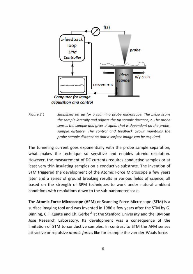
the studied sample surface as shown in Figure 2.1.
Depending on the kind of probe-sample interaction that is sensed, a vast
number of scanning probe techniques with different names have evolved. The
first SPM was a scanning tunneling microscope. It was invented by G. Binning
and H. Rohrer in 19821, 2
and senses a dc tunneling current between the
conducting probe and sample.
6
Figure 2.1 Simplified set up for a scanning probe microscope. The piezo scans
the sample laterally and adjusts the tip sample distance, z. The probe
senses the sample and gives a signal that is dependent on the probe-
sample distance. The control and feedback circuit maintains the
probe-sample distance so that a surface image can be acquired.
The tunneling current goes exponentially with the probe sample separation,
what makes the technique so sensitive and enables atomic resolution.
However, the measurement of DC-currents requires conductive samples or at
least very thin insulating samples on a conductive substrate. The invention of
STM triggered the development of the Atomic Force Microscope a few years
later and a series of ground breaking results in various fields of science, all
based on the strength of SPM techniques to work under natural ambient
conditions with resolutions down to the sub-nanometer scale.
The Atomic Force Microscope (AFM) or Scanning Force Microscope (SFM) is a
surface imaging tool and was invented in 1986 a few years after the STM by G.
Binning, C.F. Quate and Ch. Gerber3 at the Stanford University and the IBM San
Jose Research Laboratory. Its development was a consequence of the
limitation of STM to conductive samples. In contrast to STM the AFM senses
attractive or repulsive atomic forces like for example the van-der-Waals force.
2. Electrical Atomic Force Microscopy techniques
7
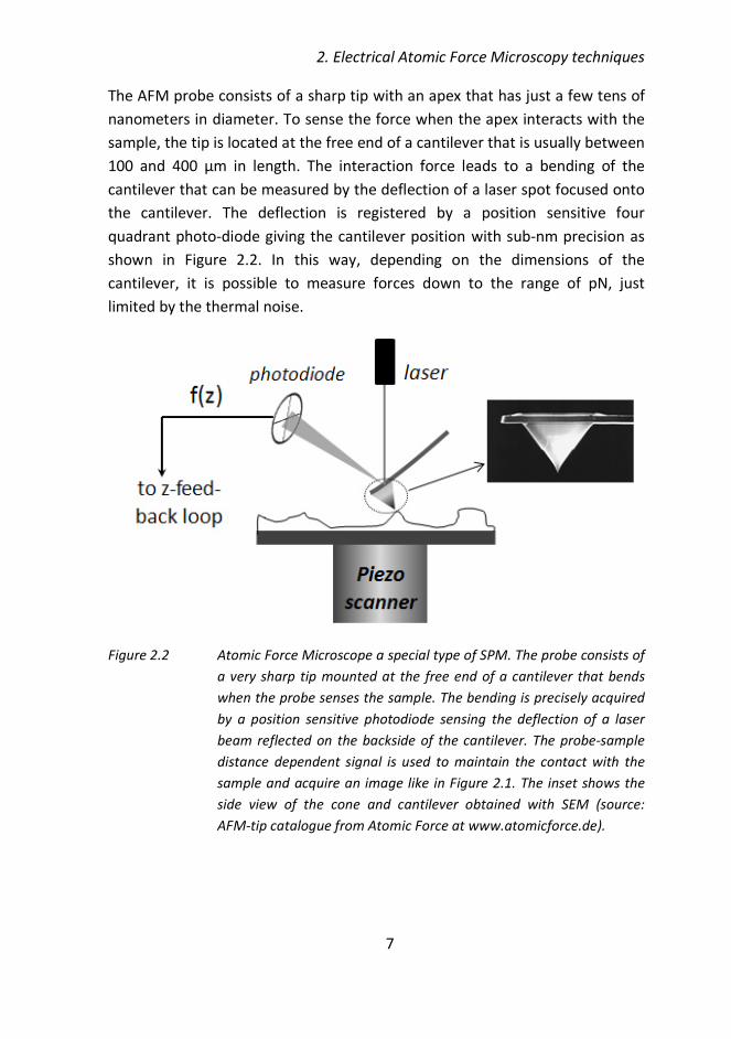
The AFM probe consists of a sharp tip with an apex that has just a few tens of
nanometers in diameter. To sense the force when the apex interacts with the
sample, the tip is located at the free end of a cantilever that is usually between
100 and 400 µm in length. The interaction force leads to a bending of the
cantilever that can be measured by the deflection of a laser spot focused onto
the cantilever. The deflection is registered by a position sensitive four
quadrant photo-diode giving the cantilever position with sub-nm precision as
shown in Figure 2.2. In this way, depending on the dimensions of the
cantilever, it is possible to measure forces down to the range of pN, just
limited by the thermal noise.
Figure 2.2 Atomic Force Microscope a special type of SPM. The probe consists of
a very sharp tip mounted at the free end of a cantilever that bends
when the probe senses the sample. The bending is precisely acquired
by a position sensitive photodiode sensing the deflection of a laser
beam reflected on the backside of the cantilever. The probe-sample
distance dependent signal is used to maintain the contact with the
sample and acquire an image like in Figure 2.1. The inset shows the
side view of the cone and cantilever obtained with SEM (source:
AFM-tip catalogue from Atomic Force at www.atomicforce.de).
8
2.1.1 AFM Topography scanning modes
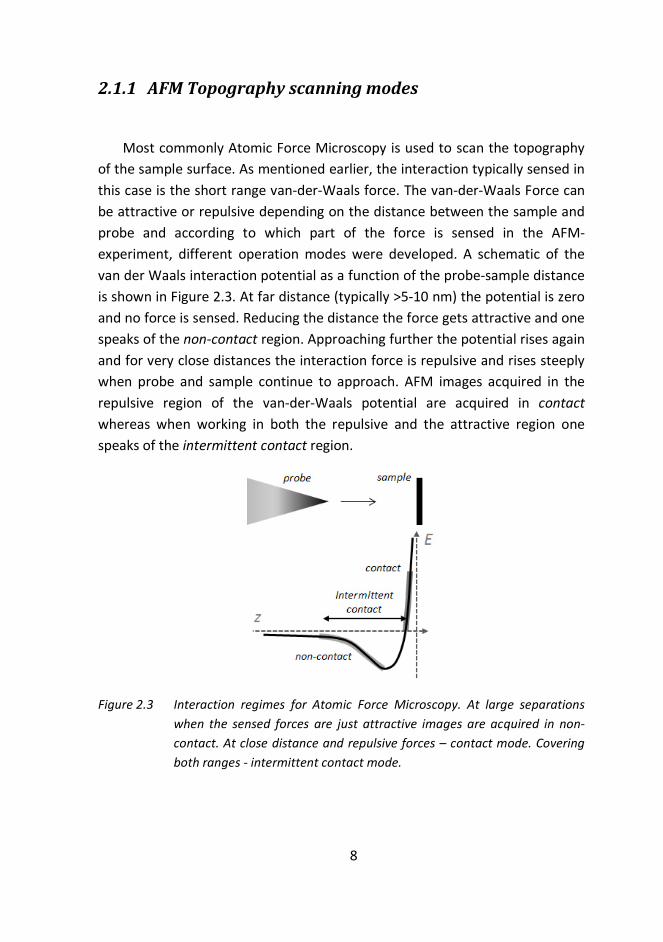
Most commonly Atomic Force Microscopy is used to scan the topography
of the sample surface. As mentioned earlier, the interaction typically sensed in
this case is the short range van-der-Waals force. The van-der-Waals Force can
be attractive or repulsive depending on the distance between the sample and
probe and according to which part of the force is sensed in the AFM-
experiment, different operation modes were developed. A schematic of the
van der Waals interaction potential as a function of the probe-sample distance
is shown in Figure 2.3. At far distance (typically >5-10 nm) the potential is zero
and no force is sensed. Reducing the distance the force gets attractive and one
speaks of the non-contact region. Approaching further the potential rises again
and for very close distances the interaction force is repulsive and rises steeply
when probe and sample continue to approach. AFM images acquired in the
repulsive region of the van-der-Waals potential are acquired in contact
whereas when working in both the repulsive and the attractive region one
speaks of the intermittent contact region.
Figure 2.3 Interaction regimes for Atomic Force Microscopy. At large separations
when the sensed forces are just attractive images are acquired in non-
contact. At close distance and repulsive forces – contact mode. Covering
both ranges - intermittent contact mode.
2. Electrical Atomic Force Microscopy techniques
9
Contact mode
Contact mode works in the repulsive region of the interaction potential. It is
usually performed with soft cantilevers (k<1N/m) to avoid the damage of the
sample surface. There are two different operation modes: The constant height
mode where the probe remains at a fixed vertical distance in contact on the
sample, while the piezo is scanning the sample in x and y direction without any
feedback activated. From the acquired deflection of the cantilever in each
point one can obtain the sample topography. This mode is preferable for very
flat samples and where fast scanning is desired. On samples with big
topography changes one has to assure that the interaction force is not
changing too much, what can lead to modifications of the probe or the sample,
and one fixes its value by defining a force set-point. An electronic feedback
between the cantilever deflection signal and the scanner elongation maintains
the force then constant. This constant-force mode is much gentler to probe
and sample, but the available scanning speed is usually limited by feedback
circuit.
Amplitude modulation mode
The amplitude modulation mode, or depending on the AFM-company also
called dynamic or tapping mode™, is operated in the intermittent contact
region. It is a dynamic mode where instead of measuring just the static
cantilever-deflection in contact, the cantilever gets excited to oscillate at its
mechanical resonance frequency. The amplitude of the oscillation gets
precisely detected by measuring the oscillation of the photodiode signal with a
lock-in amplifier. The lock-in amplifier is very sensitive, since it is able to cancel
out noise in the frequency range that does not agree with the excitation
frequency.
The excitation is usually realized in a so called acoustic mode with the help of a
small piezo mounted close to the cantilever chip. But there exist also
alternative modes that excite the cantilever oscillation by varying magnetic
10
forces (eg. MAC-Mode™) or thermally using an additional laser heating up the
cantilever and inducing a bending4, 5
. These alternative excitation modes have
been proven to be especially effective when AFM is performed in liquid
environment where sometimes the acoustic mode leads to an increased noise
and instabilities, since it excites not only cantilever oscillation modes but also
mechanical modes in the liquid.
The measured oscillation amplitude is finally used to drive the feedback that
keeps the distance between tip and sample constant. Therefore one defines a
set-point for the amplitude smaller than the oscillation amplitude out of
contact that is maintained during the scan by the feedback control-circuit as
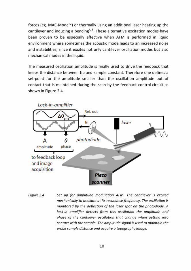
shown in Figure 2.4.
Figure 2.4 Set up for amplitude modulation AFM. The cantilever is excited
mechanically to oscillate at its resonance frequency. The oscillation is
monitored by the deflection of the laser spot on the photodiode. A
lock-in amplifier detects from this oscillation the amplitude and
phase of the cantilever oscillation that change when getting into
contact with the sample. The amplitude signal is used to maintain the
probe sample distance and acquire a topography image.
2. Electrical Atomic Force Microscopy techniques
11
The big advantage of the amplitude modulation mode is that it is less invasive
than contact mode, since the interaction can be tuned to be much softer.
There is also no lateral force present during scanning that can lead to a
modification of the sample like in contact mode. In general amplitude
modulation mode is very effective and can be used on nearly any kind of
sample allowing also the scan of very big areas. Usually cantilevers with a
higher spring constant (k>1 N/m) are used so that the resonance frequency is
high enough (fres>10 kHz) and the increased quality factor leads to good signal
to noise ratios. This is especially important in liquid where the resonance
frequency drops by about 50% due to hydrodynamic drag.
Apart from the amplitude that is used to measure the sample topography, the
lock-in also acquires the phase shift of the cantilever oscillation with respect to
the excitation signal for every image point. This phase image gives access to
additional material properties like the stiffness of the sample or the local
adhesion. These properties allow the detection of changes in the material
composition or simply differentiation of different materials that cannot be
detected by the topography.
Non-contact frequency modulation AFM
To acquire AFM-images sensing the attractive forces in the non-contact
regime, again, the cantilever has to be oscillated at its resonance frequency. To
sense the force, the microscope detects the change of the oscillation
amplitude or the shift of the cantilever resonance frequency with a phase lock
loop circuit to maintain the feedback.
To understand in more detail how the frequency shift or modulation image is
generated, one has to take a look at the mechanics of the cantilever. Assuming
the cantilever is a damped oscillator (damping γ, mass m) that gets excited by
some external periodic force Fext(t), the differential equation for the cantilever
movement satisfies, in a lumped element description:
12
( )2
2
( ) ( )( ) ext
d z t dz tm k z t F t
dt dtγ− − ⋅ = (2.1)
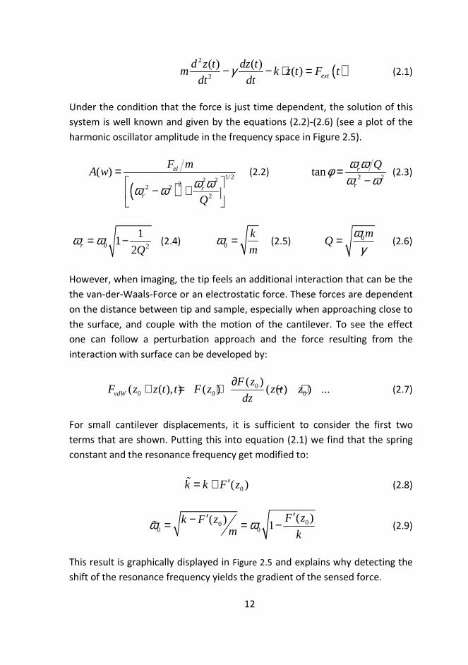
Under the condition that the force is just time dependent, the solution of this
system is well known and given by the equations (2.2)-(2.6) (see a plot of the
harmonic oscillator amplitude in the frequency space in Figure 2.5).
( )1/22 2
22 22
( ) el
rr
F mA w
Q
ω ωω ω=
− +
(2.2) 2 2
tan r
r
Qω ωφω ω
=−
(2.3)
0 2
11
2r Qω ω= − (2.4) 0
k
mω = (2.5) 0mQ
ωγ
= (2.6)
However, when imaging, the tip feels an additional interaction that can be the
the van-der-Waals-Force or an electrostatic force. These forces are dependent
on the distance between tip and sample, especially when approaching close to
the surface, and couple with the motion of the cantilever. To see the effect
one can follow a perturbation approach and the force resulting from the
interaction with surface can be developed by:
00 0 0
( )( ( ), ) ( ) ( ( ) ) ...vdW
F zF z z t t F z z t z
dz
∂+ = + − + (2.7)
For small cantilever displacements, it is sufficient to consider the first two
terms that are shown. Putting this into equation (2.1) we find that the spring
constant and the resonance frequency get modified to:
0( )k k F z′= +ɶ (2.8)
000 0
( )( ) 1F zk F z
m kω ω
′′−= = −ɶ (2.9)
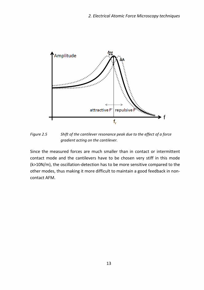
This result is graphically displayed in Figure 2.5 and explains why detecting the
shift of the resonance frequency yields the gradient of the sensed force.
2. Electrical Atomic Force Microscopy techniques
13
Figure 2.5 Shift of the cantilever resonance peak due to the effect of a force
gradient acting on the cantilever.
Since the measured forces are much smaller than in contact or intermittent
contact mode and the cantilevers have to be chosen very stiff in this mode
(k>10N/m), the oscillation-detection has to be more sensitive compared to the
other modes, thus making it more difficult to maintain a good feedback in non-
contact AFM.
14
2.2 Atomic force microscopy techniques for
electrical characterization
Like in STM it is possible to measure also electrical properties with an AFM. In
this case it is necessary to use conductive probes, additional electronics and
usually a conductive substrate to apply an electric field between the tip and
the substrate. The big advantage of AFM with respect to STM is that it offers
the possibility to measure the topography simultaneously with the electric
property of interest, because the probe sample distance can be controlled
independently. Another advantage is that also measurements on thicker
insulating samples are possible.
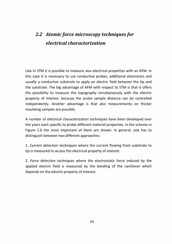
A number of electrical characterization techniques have been developed over
the years each specific to probe different material properties. In the scheme in
Figure 2.6 the most important of them are shown. In general, one has to
distinguish between two different approaches:
1. Current detection techniques where the current flowing from substrate to
tip is measured to access the electrical property of interest.
2. Force detection techniques where the electrostatic force induced by the
applied electric field is measured by the bending of the cantilever which
depends on the electric property of interest.
2. Electrical Atomic Force Microscopy techniques
15
Figure 2.6 Classification of AFM-techniques for electrical characterization. The
measured electrical property is shown with the white background.
This work is focusing on EFM-techniques.
2.2.1 Conductive Atomic Force Microscopy
In conductive Atomic Force Microscopy (C-AFM) the DC current, Idc, is
measured when applying a DC voltage between tip and substrate. To measure
Idc a current to voltage amplifier is mounted close to the tip as shown in Figure
2.7 and the tip is kept in electrical contact with the sample. In this way the
conductivity of a sample at a fixed DC-potential can be imaged while scanning
the topography in contact mode. Alternatively, it is also possible to acquire
I/V-curves on certain points of interest of the sample to study the resistivity
and its voltage dependence of the sample. A very much related technique is
scanning spreading resistance microscopy (SSRM).
16
Figure 2.7 Experimental set up for Conductive Atomic Force Microscopy.
It basically consists of the same setup and usually a logarithmic amplifier is
used to measure currents. To maintain good contact the surface is scanned
with high load. Therefore usually very hard probes with diamond coating are
used6. SSRM was mainly applied to characterize semiconductor structures
7, 8
and lateral resolutions down to one nanometer can be reached.
2.2.2 Scanning Capacitance Microscopy (SCM)
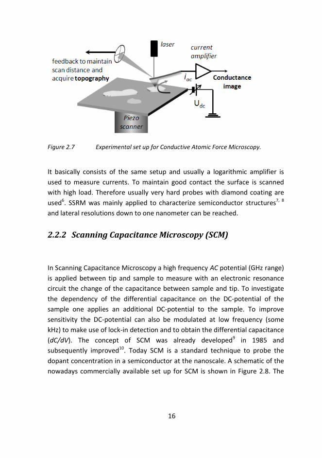
In Scanning Capacitance Microscopy a high frequency AC potential (GHz range)
is applied between tip and sample to measure with an electronic resonance
circuit the change of the capacitance between sample and tip. To investigate
the dependency of the differential capacitance on the DC-potential of the
sample one applies an additional DC-potential to the sample. To improve
sensitivity the DC-potential can also be modulated at low frequency (some
kHz) to make use of lock-in detection and to obtain the differential capacitance
(dC/dV). The concept of SCM was already developed9 in 1985 and
subsequently improved10
. Today SCM is a standard technique to probe the
dopant concentration in a semiconductor at the nanoscale. A schematic of the
nowadays commercially available set up for SCM is shown in Figure 2.8. The
2. Electrical Atomic Force Microscopy techniques
17
probe scans the sample in contact and the AC voltage is applied in parallel.
Figure 2.8 Experimental set up for Scanning Capacitance Microscopy (SCM) for
imaging the dopant concentration in a semiconductor covered by a thin
insulating oxide layer.
2.2.3 Nanoscale Impedance Microscopy (NIM)
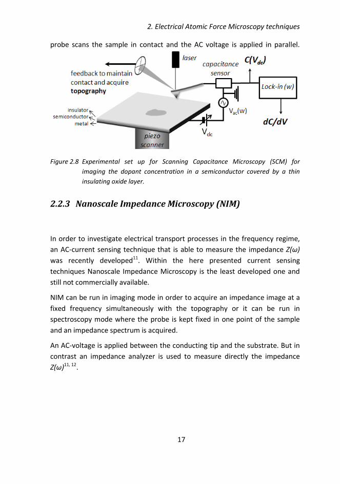
In order to investigate electrical transport processes in the frequency regime,
an AC-current sensing technique that is able to measure the impedance Z(ω)
was recently developed11
. Within the here presented current sensing
techniques Nanoscale Impedance Microscopy is the least developed one and
still not commercially available.
NIM can be run in imaging mode in order to acquire an impedance image at a
fixed frequency simultaneously with the topography or it can be run in
spectroscopy mode where the probe is kept fixed in one point of the sample
and an impedance spectrum is acquired.
An AC-voltage is applied between the conducting tip and the substrate. But in
contrast an impedance analyzer is used to measure directly the impedance
Z(ω)11, 12
.
18
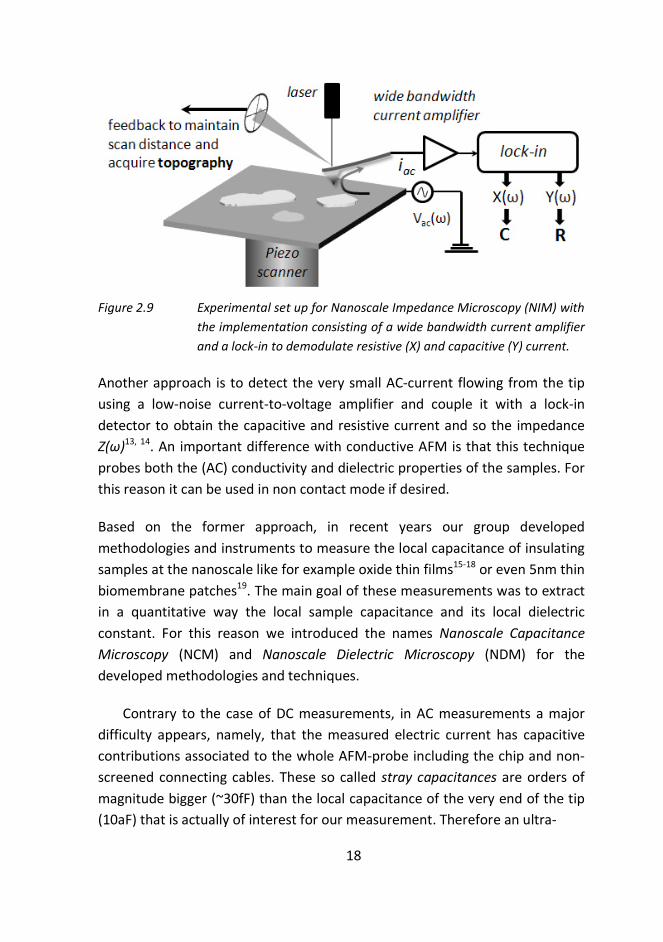
Figure 2.9 Experimental set up for Nanoscale Impedance Microscopy (NIM) with
the implementation consisting of a wide bandwidth current amplifier
and a lock-in to demodulate resistive (X) and capacitive (Y) current.
Another approach is to detect the very small AC-current flowing from the tip
using a low-noise current-to-voltage amplifier and couple it with a lock-in
detector to obtain the capacitive and resistive current and so the impedance
Z(ω)13, 14
. An important difference with conductive AFM is that this technique
probes both the (AC) conductivity and dielectric properties of the samples. For
this reason it can be used in non contact mode if desired.
Based on the former approach, in recent years our group developed
methodologies and instruments to measure the local capacitance of insulating
samples at the nanoscale like for example oxide thin films15-18
or even 5nm thin
biomembrane patches19
. The main goal of these measurements was to extract
in a quantitative way the local sample capacitance and its local dielectric
constant. For this reason we introduced the names Nanoscale Capacitance
Microscopy (NCM) and Nanoscale Dielectric Microscopy (NDM) for the
developed methodologies and techniques.
Contrary to the case of DC measurements, in AC measurements a major
difficulty appears, namely, that the measured electric current has capacitive
contributions associated to the whole AFM-probe including the chip and non-
screened connecting cables. These so called stray capacitances are orders of
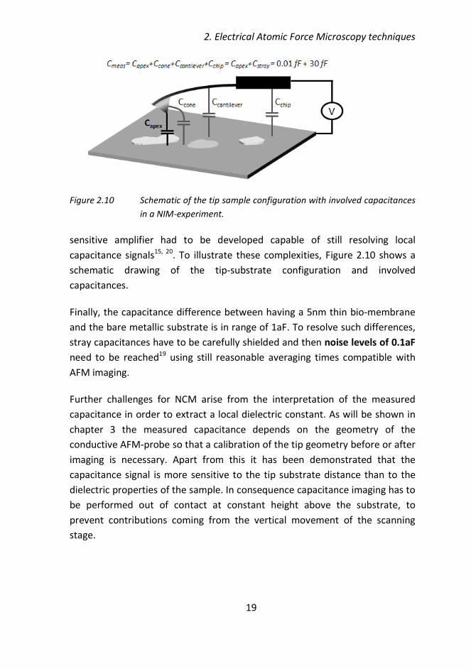
magnitude bigger (~30fF) than the local capacitance of the very end of the tip
(10aF) that is actually of interest for our measurement. Therefore an ultra-
2. Electrical Atomic Force Microscopy techniques
19
Figure 2.10 Schematic of the tip sample configuration with involved capacitances
in a NIM-experiment.
sensitive amplifier had to be developed capable of still resolving local
capacitance signals15, 20
. To illustrate these complexities, Figure 2.10 shows a
schematic drawing of the tip-substrate configuration and involved
capacitances.
Finally, the capacitance difference between having a 5nm thin bio-membrane
and the bare metallic substrate is in range of 1aF. To resolve such differences,
stray capacitances have to be carefully shielded and then noise levels of 0.1aF
need to be reached19
using still reasonable averaging times compatible with
AFM imaging.
Further challenges for NCM arise from the interpretation of the measured
capacitance in order to extract a local dielectric constant. As will be shown in
chapter 3 the measured capacitance depends on the geometry of the
conductive AFM-probe so that a calibration of the tip geometry before or after
imaging is necessary. Apart from this it has been demonstrated that the
capacitance signal is more sensitive to the tip substrate distance than to the
dielectric properties of the sample. In consequence capacitance imaging has to
be performed out of contact at constant height above the substrate, to
prevent contributions coming from the vertical movement of the scanning
stage.
20
2.2.4 Scanning Microwave Microscopy (SMM)
Scanning Microwave Microscopy (SMM) is a technique that complements NIM
at higher frequencies from 0.1-100 GHz, but its frequencies lie below those
used in optical SPM-techniques like Near-field Scanning Optical Microscopy
(NSOM) (>THz). Like NIM, also SMM has the capability to image conductivity
and dielectric properties at the nanoscale. Nanoscale studies with SMM have
been conducted on different types of materials reaching from solid state
materials to biological samples21, 22
. SMM has been made only recently
available on commercial AFM-products. In SMM the magnitude measured is
the microwave scattering parameters (S-parameters) which can be related to
the local impedance of the probe substrate system.
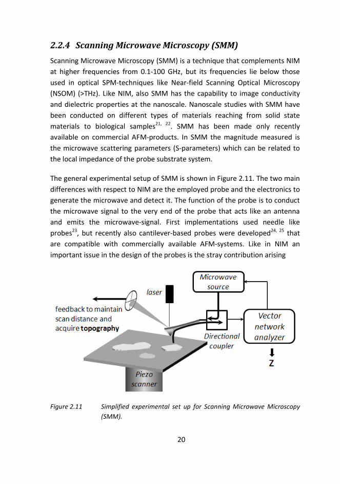
The general experimental setup of SMM is shown in Figure 2.11. The two main
differences with respect to NIM are the employed probe and the electronics to
generate the microwave and detect it. The function of the probe is to conduct
the microwave signal to the very end of the probe that acts like an antenna
and emits the microwave-signal. First implementations used needle like
probes23
, but recently also cantilever-based probes were developed24, 25
that
are compatible with commercially available AFM-systems. Like in NIM an
important issue in the design of the probes is the stray contribution arising
Figure 2.11 Simplified experimental set up for Scanning Microwave Microscopy
(SMM).
2. Electrical Atomic Force Microscopy techniques
21
from the nonlocal parts of the tip (like cantilever and so on) that have to be
shielded to improve sensitivity21
.
There are different solutions to realize the electronics detecting the
microwave signal. The implementation that is commercially available from
Agilent Technologies consists of a network analyzer that sends a microwave
signal through a diplexer to the probe. The signal gets reflected and travels
through the tip back to the network analyzer where it gets separated into the
reflection scattering coefficient (S11) which is related to the local impedance
probed by the tip. Typical noise levels of such setups are in the range of 1aF22
.
One of the great difficulties in SMM is like in NIM the quantitative extraction of
the electric and dielectric properties of the sample from the measured
impedances. Therefore adequate models have to be developed that take into
account the specific tip geometry. This goal can be achieved to some extend by
analytical approximations and finite element modeling26, 27
22
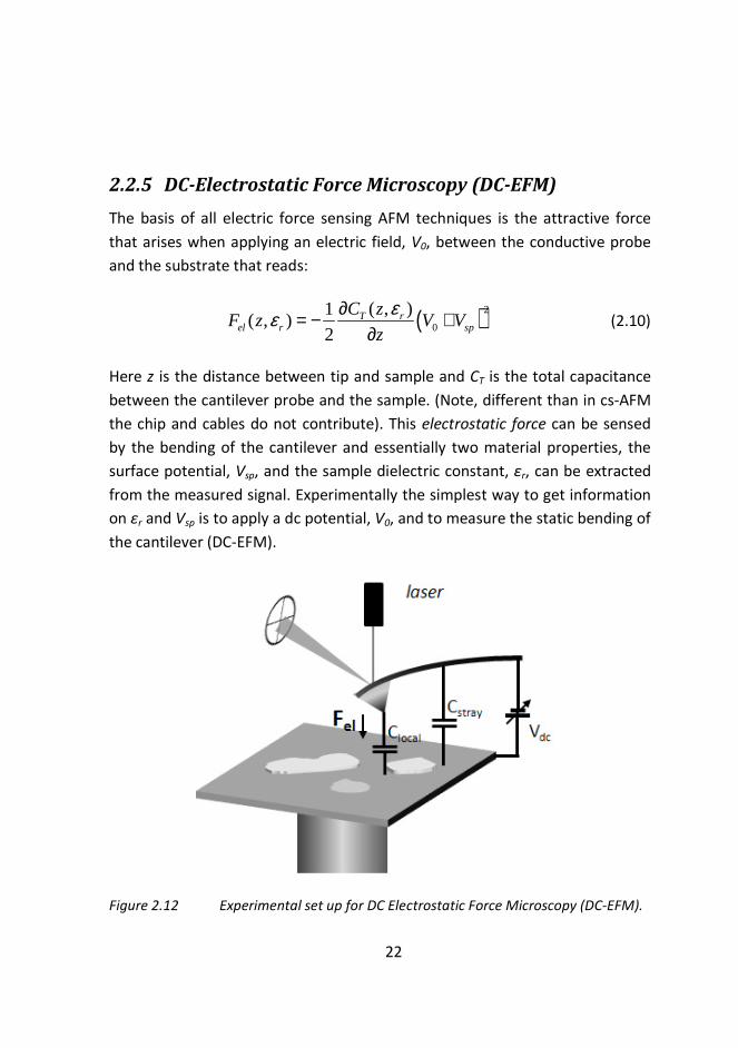
2.2.5 DC-Electrostatic Force Microscopy (DC-EFM)
The basis of all electric force sensing AFM techniques is the attractive force
that arises when applying an electric field, V0, between the conductive probe
and the substrate that reads:
( )2
0
( , )1( , )
2T r
el r sp
C zF z V V
z
εε ∂= − +∂
(2.10)
Here z is the distance between tip and sample and CT is the total capacitance
between the cantilever probe and the sample. (Note, different than in cs-AFM
the chip and cables do not contribute). This electrostatic force can be sensed
by the bending of the cantilever and essentially two material properties, the
surface potential, Vsp, and the sample dielectric constant, εr, can be extracted
from the measured signal. Experimentally the simplest way to get information
on εr and Vsp is to apply a dc potential, V0, and to measure the static bending of
the cantilever (DC-EFM).
Figure 2.12 Experimental set up for DC Electrostatic Force Microscopy (DC-EFM).
2. Electrical Atomic Force Microscopy techniques
23
In principle to extract for example εr from the force signal, Vsp has to be
already known, but when working with high applied DC-voltages the error
induced by an unknown Vsp is negligible.
Also, the sensitivity is limited by thermal and other, for example electronic
noise. However, it is a very clear and simple method, as I will show in detail in
chapter 4 and it is possible to extract a quantitative value of the dielectric
constant of thin insulating films from measurements in this mode.
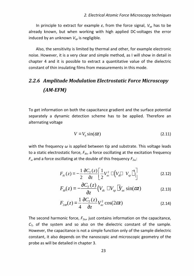
2.2.6 Amplitude Modulation Electrostatic Force Microscopy
(AM-EFM)
To get information on both the capacitance gradient and the surface potential
separately a dynamic detection scheme has to be applied. Therefore an
alternating voltage
0 sin( )V V tω= (2.11)
with the frequency ω is applied between tip and substrate. This voltage leads
to a static electrostatic force, Fdc, a force oscillating at the excitation frequency
Fω and a force oscillating at the double of this frequency F2ω:
( )22( )1 1( )
2 2T
dc ac dc sp
C zF z V V V
z
∂ = − + + ∂ (2.12)
( )( )( ) sin( )T
dc sp ac
C zF z V V V t
zω ω∂= − +∂
(2.13)
22
( )1( ) cos(2 )
4T
ac
C zF z V t
zω ω∂=∂
(2.14)
The second harmonic force, F2ω, just contains information on the capacitance,
CT, of the system and so also on the dielectric constant of the sample.
However, the capacitance is not a simple function only of the sample dielectric
constant, it also depends on the nanoscopic and microscopic geometry of the
probe as will be detailed in chapter 3.
24
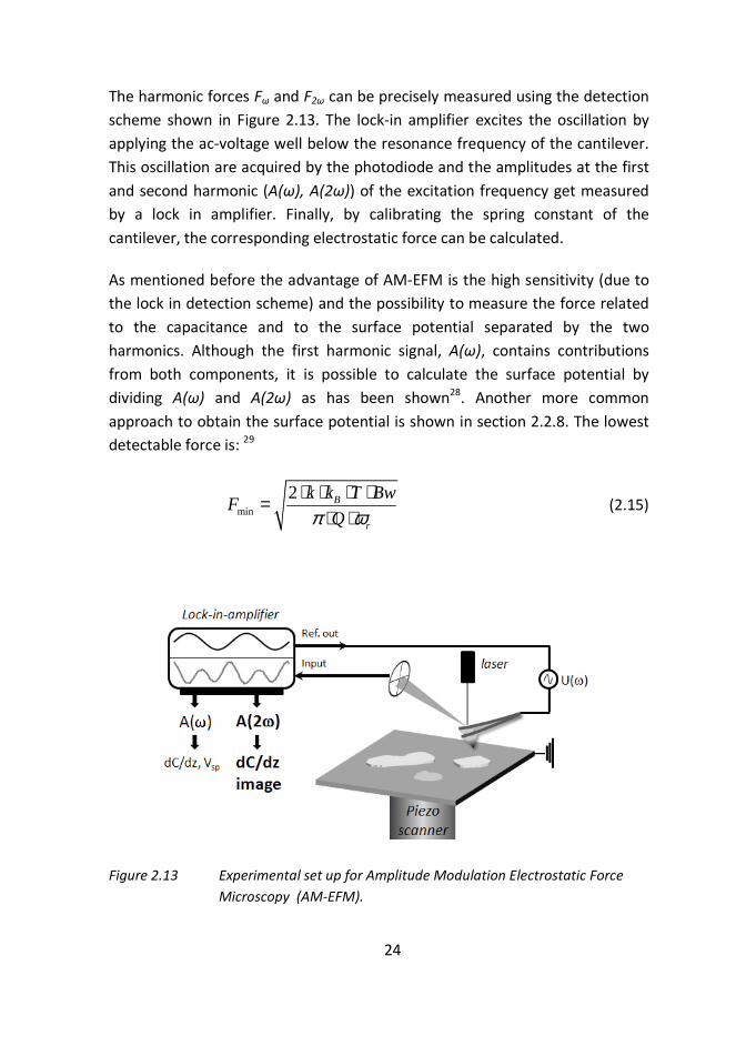
The harmonic forces Fω and F2ω can be precisely measured using the detection
scheme shown in Figure 2.13. The lock-in amplifier excites the oscillation by
applying the ac-voltage well below the resonance frequency of the cantilever.
This oscillation are acquired by the photodiode and the amplitudes at the first
and second harmonic (A(ω), A(2ω)) of the excitation frequency get measured
by a lock in amplifier. Finally, by calibrating the spring constant of the
cantilever, the corresponding electrostatic force can be calculated.
As mentioned before the advantage of AM-EFM is the high sensitivity (due to
the lock in detection scheme) and the possibility to measure the force related
to the capacitance and to the surface potential separated by the two
harmonics. Although the first harmonic signal, A(ω), contains contributions
from both components, it is possible to calculate the surface potential by
dividing A(ω) and A(2ω) as has been shown28
. Another more common
approach to obtain the surface potential is shown in section 2.2.8. The lowest
detectable force is: 29
min
2 B
r
k k T BwF
Qπ ω⋅ ⋅ ⋅ ⋅=
⋅ ⋅ (2.15)
Figure 2.13 Experimental set up for Amplitude Modulation Electrostatic Force
Microscopy (AM-EFM).
2. Electrical Atomic Force Microscopy techniques
25
(kB Boltzmann constant, T temperature, Bw lock-in bandwidth, Q cantilever
quality factor, ωr resonance frequency).So for typical values of k=0.1 N/m,
Bw=100 Hz, Q=100 and ωr=30 kHz would give Fmin=0.1 pN or with Vac=3 V the
minimal detectable capacitance gradient is dCT,min/dz= 0.02 zF/nm. This is
almost four orders of magnitude better than what is currently possible with
current sensing methods.
2.2.7 Frequency Modulation Electrostatic Force Microscopy
(FM-EFM)
Apart from the amplitude modulation mode, EFM can also be operated in
frequency modulation mode what can improve the resolution of the electric
image. As has been shown in section 2.1.1, an electrostatic force acting on the
cantilever leads to a modification of the spring constant, k, what leads to a
frequency shift of the resonance frequency. The measured frequency shift, Δω,
is related to the force gradient by30
:
0
2
F
k z
ωω ∂∆ =∂
(2.16)
where ω0 the free resonance frequency and z the probe-sample separation.
This shift oscillates with the frequency of the applied electric potential and can
be detected. The experimental realization of FM-EFM is schematically shown
in Figure 2.14. It requires two lock-in amplifiers. Like in AM-EFM one applies
with a first lock-in the alternating electric field of the frequency ωel between tip
and sample. Simultaneously, the cantilever is excited mechanically at its
resonance frequency by the second lock-in. The electrical excitation leads to a
shift of the mechanical resonance frequency that oscillates with ωel (Δωr=Δωr,0
sin(ωelt)). Notice, ωel should be clearly lower than the resonance frequency.
The oscillating resonance frequency gets locked by the second lock-in using a
phase lock loop circuit. This signal is fed into the first lock-in where the
amplitude of the frequency shift, Δωr,0, is measured.
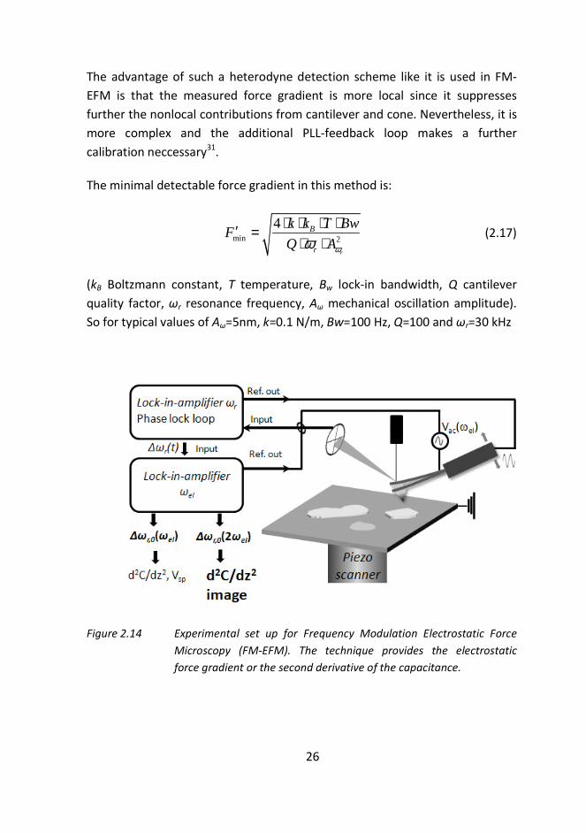
26
The advantage of such a heterodyne detection scheme like it is used in FM-
EFM is that the measured force gradient is more local since it suppresses
further the nonlocal contributions from cantilever and cone. Nevertheless, it is
more complex and the additional PLL-feedback loop makes a further
calibration neccessary31
.
The minimal detectable force gradient in this method is:
min 2
4
r
B
r
k k T BwF
Q Aωω⋅ ⋅ ⋅ ⋅′ =
⋅ ⋅ (2.17)
(kB Boltzmann constant, T temperature, Bw lock-in bandwidth, Q cantilever
quality factor, ωr resonance frequency, Aω mechanical oscillation amplitude).
So for typical values of Aω=5nm, k=0.1 N/m, Bw=100 Hz, Q=100 and ωr=30 kHz
Figure 2.14 Experimental set up for Frequency Modulation Electrostatic Force
Microscopy (FM-EFM). The technique provides the electrostatic
force gradient or the second derivative of the capacitance.
2. Electrical Atomic Force Microscopy techniques
27
would give Fmin=0.05 pN/nm or with Vac=3 V the minimal detectable
capacitance gradient is d2CT,min/dz2=0.01 zF/nm2.
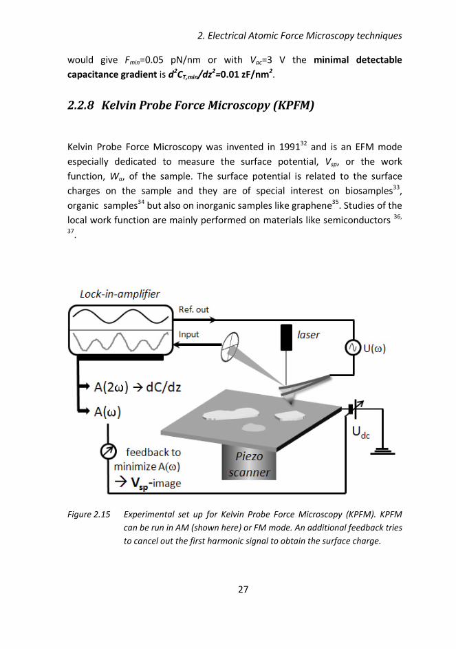
2.2.8 Kelvin Probe Force Microscopy (KPFM)
Kelvin Probe Force Microscopy was invented in 199132
and is an EFM mode
especially dedicated to measure the surface potential, Vsp, or the work
function, Wa, of the sample. The surface potential is related to the surface
charges on the sample and they are of special interest on biosamples33
,
organic samples34
but also on inorganic samples like graphene35
. Studies of the
local work function are mainly performed on materials like semiconductors 36,
37.
Figure 2.15 Experimental set up for Kelvin Probe Force Microscopy (KPFM). KPFM
can be run in AM (shown here) or FM mode. An additional feedback tries
to cancel out the first harmonic signal to obtain the surface charge.
28
The experimental set up for KPFM is the same like in FM-EFM or AM-EFM, but
in order to get direct access to the local surface potential or work function, an
additional feedback is applied that tries to minimize the first harmonic
amplitude A(ω) by applying a dc potential at the sample as shown in Figure
2.15. The first harmonic amplitude is exactly zero when the dc-potential is
opposite of the surface potential, as can be seen from equation (2.13).
The applied DC-potential is acquired simultaneously with the topography and
gives direct access to the surface potential without further calculations.
KPFM images can be acquired in two different scanning modes. Either in a
single pass mode in tapping acquiring simultaneously topography and surface
potential in the same scan line or alternatively in a double pass mode, the so
called lift mode™ acquiring first the topography and then retracing the last
scan line just lifted a few tens of nanometers above it. The advantage of the
single pass method is its speed and higher resolution, however with certain
samples there the chance to have crosstalk between topography and surface
charge. Today, KPFM is available, both in frequency and amplitude
modulation, on many commercially available AFMs. However, its application is
limited to the use in vacuum or air.
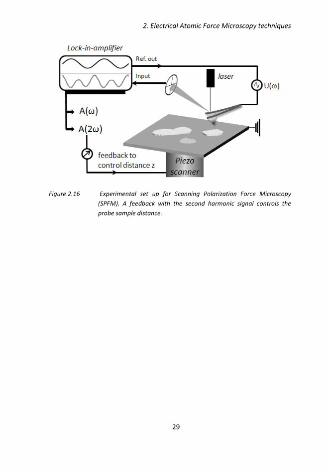
2.2.9 Scanning Polarization Force Microscopy (SPFM)
Scanning Polarization Force Microscopy is an EFM technique that was
developed in 199438
and was extensively used to image very thin and soft
dielectric materials like water layers39, 40
that are difficult or impossible to
image with conventional AFM-modes. It takes advantage of the relative long
range of the electrostatic interaction compared to the van der Waals force in
order to realize a real non-contact measurement of the sample. The used
experimental set up is similar to the am-EFM set up, but by applying a
feedback between the measured A(2ω)-signal and the controller of the piezo
z-movement the probe-sample distance is controlled like shown in Figure 2.16.
Beside the topography also variations of the ionic mobility and the surface
potential can be measured41-43
when an additional feedback is applied like in
KPFM.
2. Electrical Atomic Force Microscopy techniques
29
Figure 2.16 Experimental set up for Scanning Polarization Force Microscopy
(SPFM). A feedback with the second harmonic signal controls the
probe sample distance.
30
2.2.9.1 AFM techniques for electrical
characterization in liquid
The study of nanoscale material properties in their natural liquid environment
is one of the most import reasons why scanning probe microscopy has become
so popular in life science. A liquid and ion-containing environment is not only
the natural environment of many organic and inorganic specimen and allows
so more realistic studies, it also enables for example (electro)-chemical
reactions to take place and therefore to study the specimen in function.
When moving with the AFM from dry into ion containing liquid environment a
number of electrical properties change. The most evident one is that the water
provides a media where ions and electro-active species can dissociate and
move, what leads to a solution conductivity, σ, of the media and to the
possibility of electrochemical reactions. Another point is that the dielectric
constant of water is clearly higher than in air (εr,water~78 versus εr,air=1). Finally,
a very important and particular aspect of ionic water-solutions is the formation
of electrical double layers.
An electrical double layer (or just double layer) is formed when a metallic
electrode surface is exposed to an electrolyte solution. Excess charges from
the metal form a space charge region that gets compensated by the
adsorption of counter ions from the solution to reach a thermodynamic
equilibrium.
2. Electrical Atomic Force Microscopy techniques
31
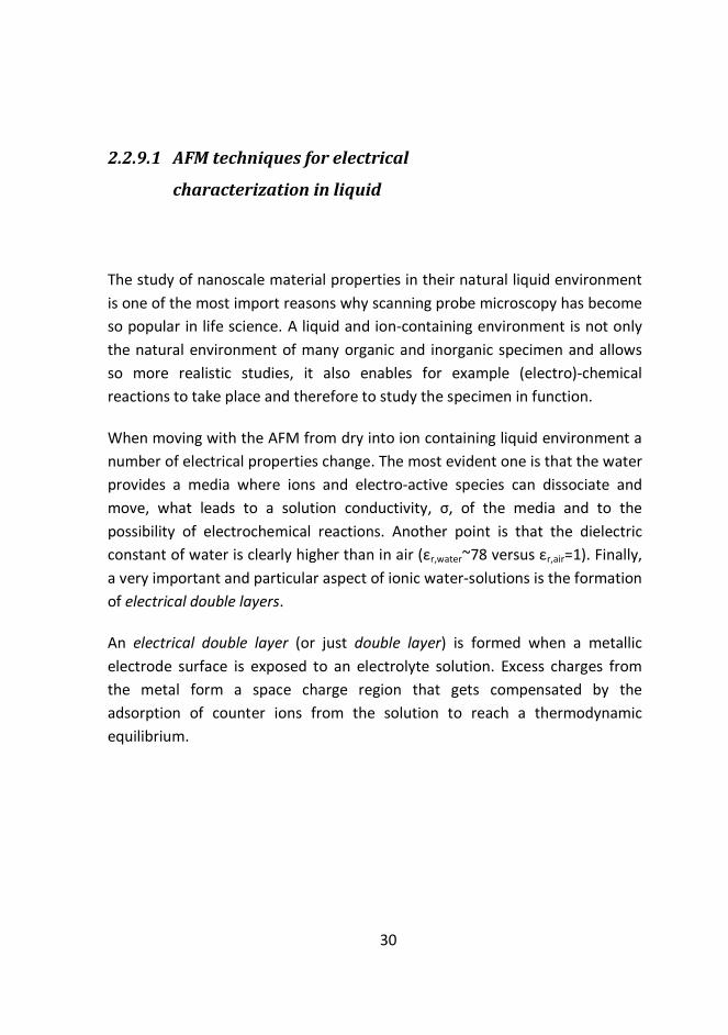
Figure 2.17 (a) Cartoon of the electrical double layer developing at the charged
metal interface. (b) Potential distribution in the double layer: Until the
Outer Helmholtz Layer the potential drops off linearly. In the diffuse
layer it drops off exponentially. (c) The Double Layer Capacitance in
dependency of the electrode potential.
The locus of this single layer of ions is the so called Inner Helmholtz Plane
(IHP). The dipoles formed by these two opposite space charge layers attract
solvated ions. These solvated ions experience an attractive force, but also
possess thermal energy so that they still diffuse around randomly. However,
they cannot get closer to the electrode surface than to the so called Outer
Helmholtz Plane (OHP). The solvated ions, that form the so called diffuse layer,
exhibit a from the electrode surface nearly exponentially decaying
concentration distribution, as shown in Figure 2.17b. In consequence, also the
potential drops off in this way. In the limit of small electrode potentials
(φ<50mV), the potential decay with the distance x is:
1/2/ 0
0 2 2 0
0.304( ) ;
2 [ / ]Dx B r
D
k T nmx e
z e n z c mol Lλ ε εφ φ λ− = ⋅ = ≈ ⋅
(2.18)
Here, e is the elementary charge, z the number of charges per ion, n0 the
charge concentration, kB the Boltzmann constant, T the temperature, φ0 the
electrode potential and c the concentration. The characteristic length of this
32
decay is defined by the Debeye Length, λD, that is just 10 nm short for
concentrations of 1mM.
As derived for example in detail in textbooks like Electrochemical Methods
from Bard & Faulkner44
the space charge regions and the diffuse layer lead to
the formation of the so called Helmholtz Capacitance45
, CH, and the Gouy-
Chapman-Capacitance46
, CG.
0 rH
OHP
Cd
ε ε= (2.19)
1/22 2 0202
cosh 228 / [ / ] cosh(19.5 )2
rG
B B
z e n zeC F cm z c mol l z
k T k T
ε ε φ µ φ
= ≈
(2.20)
Both capacitances are in series and form the total double layer capacitance, Cd.
Also important to notice, the double layer capacitance in this model is
potential depend as it was also suggested by experimental observations. It
takes its lowest value at the potential of zero charge, φPZC, a characteristic
value for every material. For high voltages it gets limited by the Helmholtz
capacitance as shown in Figure 2.17c.
This short overview about the properties of the electric double layer should
show that the potential distribution at the solution/electrode interface is
clearly different than in air. The electric double layer leads to a rapid decay of
applied potentials so that electrostatic forces are effectively shielded. This has
also consequences when detecting electrical currents instead of forces.
I want to emphasize that the above considerations are only strictly valid under
static conditions. As reviewed for example by Bazant et al.47-49
and others50
, at
higher frequencies other effect have to be taken into account. In chapter 6 I
will also show that under certain conditions for force measurements the effect
of double layer capacitance can be neglected.
2. Electrical Atomic Force Microscopy techniques
33
Scanning Electrochemical Microscopy (SECM)
The most common current sensing AFM-technique in liquid is probably
Scanning Electrochemical Microscopy (SECM). Although some SECMs are
commercially available, they are often only operated at the microscale since
nanometric SECM-probes are difficult to manufacture. SECM is used to probe
local electrochemical reactions by applying specific electrochemical potentials
to the metallic probe and/or sample using a potentiostat.
To access also the nanoscale, different implementations of the probe have
been reported, some using tuning forks in combination with
ultramicroelectrodes to acquire topography and electrochemical current
simultaneously51
, others use cantilever-tips containing just a small exposed
electrode-part close to the apex to sense the current52
. Though, SECM-AFM is
mainly used to sense dc-currents of electrochemical reaction. Only a small
number of works apply alternating electric fields and measure the frequency
dependent current in AC-SECM. These studies were recently reviewed by
Eckhard and Schuhmann53
. However, none of these works deals with the
measurement of dielectric properties of the sample; instead they are centered
on the resistive component of the current.
Scanning Microwave Microscopy in liquid (SMM)
Scanning Microwave Microscopy has the great capability to image conductivity
but also dielectric properties of the sample under study and this at still
relatively low frequencies compared to optical techniques like for example in
NSOM. The big difficulty for the operation in liquid solutions consists on the
one hand in having probes being sufficiently sensitive to the sample and at the
same time keeping the capability to scan the topography. Indeed, recently it
has been shown that at the micrometer scale a scanning microwave
microscopy can be also operated in liquid using a NSOM-like tuning fork
detector to control the tip sample distance54
. Maybe in the near future it will
be possible to increase the resolution of such systems and also cantilever
based probes in principle might be operative in liquid at some point.
34
On the other hand a mayor complexity lies in the very different electric
properties in solution (high conductivity and dielectric constant) that will also
require new theoretical models in order to reach quantitative results like in air.
For these reasons until now, SMM has not been shown to provide quantitative
dielectric imaging in liquid environment.
2.2.10 Electrostatic Force Microscopy in liquid
The formation of the electrical double layer at the surface of a two charged
electrode surfaces separated a certain distance z from each other, leads to the
development of an electrostatic force55, 56
. Using an AFM these forces can be
measured and quantified assuming the AFM-tip to be a cone with a sphere as
apex and solving the Poisson-Boltzmann equation. Therefore one has to
assume that either tip and substrate are at constant potential (cp) or that they
have a constant charge (cc). Then, as has been shown further revised by Butt
et al.57, 58
, the force evolving from the double layer interaction of such a tip
with a planar surface is:
22 2
0
22 ( )D Dz zcc D
el s t s tr
RF e eλ λπλ σ σ σ σ
ε ε− − = + + (2.21)
22 2022 ( )D Dz zcp r
el s t s tD
RF e eλ λπ ε ε ψ ψ ψ ψ
λ− − = − + (2.22)
In these equation ψt (σt) and ψs (σs) is the potential (surface charge) of the tip
and the substrate, respectively, R the apex radius and λD is the Debye length,
introduced earlier. Recently, also alternative approaches like the constant
regulation approximation59
that combine both conditions were proposed.
By the direct measurement of these double layer forces with AFM, a number
of studies have contributed in the last 20 years a lot to the basic understanding
of charged interfaces in electrolyte solutions. Investigations were carried out
studying the electric double layer of noble metals like gold60-66
for various sorts
2. Electrical Atomic Force Microscopy techniques
35
of ions and concentrations applying different DC-potentials at the sample with
a (bi-)potentiostat. Also other materials like HOPG62
, semiconductors67
or gold
with thin adsorbed SAM-layers68
were studied. As mentioned, most of these
publications were performed under potential control using a potentiostat.
Other authors worked with insulating AFM-tips (SiN) and substrates (mica) in
the constant charge condition, investigating for example the surface charges of
phospholipid-membranes69-71
. In these studies, images of the electrostatic
double layer interaction-force acquired in lift mode, show that it is possible to
distinguish different types of phospholipids by their surface charge. It was also
argued, that the dipole potential of the phospholipid-headgroup can be
measured70
. In other works patches of bacteria membrane were studied72
.
Also recently, DNA molecules on flat substrates could be resolved sensing their
electric double layer71, 73
.
However, all studies mentioned so far in this section were performed
measuring the static double layer interaction and so probing the surface
charges. In contrast, almost no work is dealing with the detection of the AC
electrostatic force like it can be performed with AM-EFM in air (cp. section
2.2.6). The first who tried to perform AM-EFM in liquid by using a
bipotentiostat were Hirata et al.74
They could show for solutions of very low
ion concentration (c<0.1mM) and at low frequency that one can measure
some electrostatic force and they acquired force versus distance curves.
Nevertheless, the origin of this force was not clear and the same theoretical
background like in air was used to interpret the experiments. Indeed studies
from Raiteri et al.75
indicate that the measured forces are mainly induced by
electrochemical surface stress of the cantilever or the presence of
electrochemical reactions. Also other authors follow this argumentation76
.
However, recently a new method was proposed77
to the probe surface charge
in the AM-EFM mode but using slightly higher frequencies up to 30 kHz. As will
be shown in chapter 6, I share the idea to use higher frequencies to perform
AC-EFM in ionic solution with the aim to investigate dielectric sample
properties, but theoretical considerations will show that much higher
frequencies are necessary to obtain measurements sensitive to the local
dielectric properties from the sample.
36
2.3 Quantitative dielectric material properties from
electrical AFM-based techniques.
One of the most important properties of an insulating material is its relative
permittivity also referred to as dielectric constant, εr. It represents how electric
dipoles in a given medium react on an external electric field and how they
change their orientation and polarize according to the field. This is expressed
by the equation
0 0rD E E Pε ε ε= = + (2.23)
where D is the electric displacement field, ε0 the vacuum permittivity, E the
electric field and P the polarization (the second equality is valid for linear
isotropic materials). It is important to notice that the dielectric constant is a
material property that is related to the microscopic structure of the material
under study and how fast this structure changes into its new orientation upon
an applied electric field. The response time of the process is called the
relaxation time. This means that the dielectric constant is time-or frequency
dependent. Indeed, εr is a dielectric function dependent on the frequency of
the applied field and can be written in the form:
( ) ( ) ( )iε ω ε ω ε ω′ ′′= + . (2.24)
The real part ε ′ is related to the stored energy in the media, while dissipation
is characterized by the imaginary part ε ′′ . The form of this dielectric function
depends on which dipole in the material has to be polarized:
In Electronic and atomic polarization the electric field displaces the center of
charge of the electrons with respect to the nucleus or opposite charged atoms
in a molecule. This take place up to very high frequencies (infrared to visual
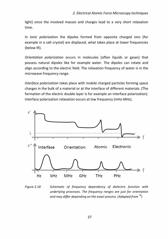
2. Electrical Atomic Force Microscopy techniques
37
light) since the involved masses and charges lead to a very short relaxation
time.
In Ionic polarization the dipoles formed from opposite charged ions (for
example in a salt crystal) are displaced, what takes place at lower frequencies
(below IR).
Orientation polarization occurs in molecules (often liquids or gases) that
possess natural dipoles like for example water. The dipoles can rotate and
align according to the electric field. The relaxation frequency of water is in the
microwave frequency range.
Interface polarization takes place with mobile charged particles forming space
charges in the bulk of a material or at the interface of different materials. (The
formation of the electric double layer is for example an interface polarization).
Interface polarization relaxation occurs at low frequency (mHz-MHz).
Figure 2.18 Schematic of frequency dependency of dielectric function with
underlying processes. The frequency ranges are just for orientation
and may differ depending on the exact process. (Adapted from 78
)
38
In order to measure the dielectric constant of a material at the nanoscale one
has to relate the measured current or force to the dielectric properties of the
material through an appropriate theoretical model that takes into account the
probe geometry and, eventually, the sample geometry.
In measurements in air environment a number of recent works have been
dealing with this aspect. Again one has to distinguish between measurement
of dielectric samples adsorbed on conducting substrates and samples
adsorbed on thick insulating substrates.
Metallic Substrates
The electrostatic force on the AFM-tip above a bare metallic substrate has
been studied extensively in the past. First simple analytical models that tried
to approximate the AFM-tip as a sphere above a plane79
where replaced by
more complex models like the cone model from Hudlet et al.80
as will be
detailed also in the next chapter.
However, for the case of a thin dielectric samples supported by the metallic
substrate just a few models are available. Various approaches have been made
like assuming the tip-sample geometry to be a simple parallel plate capacitor
with two dielectrics – one representing the air and the other the thin film.
Krayev et al. 81, 82
proposed another model consisting of a spherical capacitor
with two dielectrics representing the air and the thin dielectric film. The
advantage of these analytical models is their simplicity. Recently our group
presented another analytical approximation for thin dielectric films that is
related to the Hudlet-formula18
and will be detailed in chapter 3. Although the
accuracy of this analytical approximation is good, its applicability is a bit
limited to certain experimental conditions. Another completely different
approach consists in performing numerical calculations and simulations to
compare them with the experimental results and finally extract the dielectric
constant of the sample 31, 83
. In this case, usually the tip geometry is
determined in a separate calibration step and the simulation is performed with
the extracted specific geometry.
2. Electrical Atomic Force Microscopy techniques
39
Thick Dielectric Substrates
For thick dielectric substrates clearly less quantitative models are available.
Actually, until now, no work has been published quantifying the dielectric
constant of a thin dielectric sample on top of a thick insulating substrate.
Studies are still concentrating on the electrostatic problem of a AFM-probe
above the bare dielectric substrate. Experiments showed that a simple parallel
plate model which would lead to zero force for very thick substrates does not
describe the physical reality. Other analytical models, like those of a sphere
above an infinite dielectric84
, show at least the qualitative agreement with
experimental observations and the force does not vanish for very thick
substrates and tends to get independent from the thickness. However,
quantitative agreement is not reached.
Again, more realistic and therefore more quantitative models could be
obtained using numerical calculations using the generalized image-charge
method as reported in Ref.85
In this article the importance to include not only
the apex but also the cone is emphasized, since although it is not contributing
directly to the measured force, it may have an indirect effect. Another work is
dealing with the indirect effect, additionally, an infinite cantilever would have
for the measured force86
.
However, so far no closed methodology was reported to quantitatively extract
the absolute value of the dielectric constant from thick insulators by
electrostatic force or capacitance measurements. The work on the
development of such a methodology is described in chapters 3 and 5.
40
2.4 Motivation and Objectives of this work
As shown in this chapter, AFM is an extremely versatile tool to investigate
electric properties at the nanoscale and hence constitutes a good candidate
technique to approach the quantification of the nanoscale dielectric properties
of biomembranes. Although a few AFM techniques exist capable of
investigating polarization properties, it remains difficult to extract quantitative
values of εr from the measurements, and most importantly, they do not work
in the liquid environment.
One reason for this is on the instrumental side, since for studies at the
nanoscale very small quantities have to measured, that can be easily
overwhelmed by electronic noise as it maybe for example the case in current
sensing based techniques. Electrostatic Force sensing techniques may in
principle have an advantage here, since the used cantilevers for force
detection are extremely sensitive and naturally, undesired nonlocal electrical
signals from the cantilever are suppressed.
Another important aspect is attributed to a lack of sufficiently precise
quantitative models to relate measured force with the dielectric constant
value of the sample. Indeed, for measurements on insulating substrates like
mica or glass that are sometimes required for biological samples, still no
quantitative model is available. Moreover, successful measurements of
dielectric properties in liquid media, that is fundamental for the functionality
of some biological samples, has not been shown until now.
As consequence of the existing limitations for quantitative dielectric imaging
the objectives of this work were to extend the quantitative capabilities of
Electrostatic Force Microscopy to image the dielectric constant of
biomembranes with nanoscale spatial resolution. In particular, I addressed
four objectives:
2. Electrical Atomic Force Microscopy techniques
41
1. To evaluate the possibility to perform quantitative dielectric
measurement of biomembranes on metallic substrates and in air with
Electrostatic Force Microscopy that may offer higher precision with
respect to current sensing techniques.
2. To extend the applicability of quantitative dielectric measurement to
the case of thick insulating substrates in order to facilitate its use with
biomembranes that cannot be prepared on metallic substrates.
3. To develop a setup for dielectric imaging in liquid environment based
either on direct current detection or on the principles of electrostatic
force microscopy.
4. To perform nanoscale dielectric measurements on biomembranes in
their natural liquid environment.

42
3. Quantitative Electrostatic Force Microscopy
43
3 Quantitative Electrostatic Force Microscopy
The main goal of this work and of the work of our research group is the
quantitative extraction of the dielectric constant on biomembranes and other
samples. As mentioned earlier, one important issue, apart from the
measurement itself, is the interpretation of the obtained dC/dz-image or
curve. This is because the dC/dz-signal depends apart from the dielectric
constant also strongly on the probe-geometry. For this reason, using the
dC/dz-image alone, in principle, it is just possible to make comparative
measurements stating that one material has a higher dielectric constant than
the other – and this only in the case that for the measurements the same
unmodified AFM-tip has been used and the sample geometry is not different.
Therefore, to obtain a good quantitative estimation of the absolute dielectric
constant value independently of the used AFM-tip, it is necessary to apply a
calibration procedure to extract first of all the effective tip-geometry to
subsequently convert the dC/dz-image into a quantitative dielectric image.
In what follows, I will shortly review the different analytical approximations
that relate the measured electrostatic force for a conductive AFM-tip above a
conductive substrate with the tip geometry.
As mentioned earlier, when calculating the dielectric constant with the
calibrated geometry and the dC/dz-image, analytical expressions are only
available for a limited number of sample geometries. In the case no analytical
model is available, finite element simulations can be used that are capable to
calculate the electrostatic force for any geometry – although being clearly less
flexible in usage. In order to cope with this drawback I developed in context
with my work a number of finite element models (FEM) and scripts offering
now almost the same flexibility and applicability like an analytical expression.
44
3.1 Analytical approximations of the probe-
substrate force
Metallic substrates
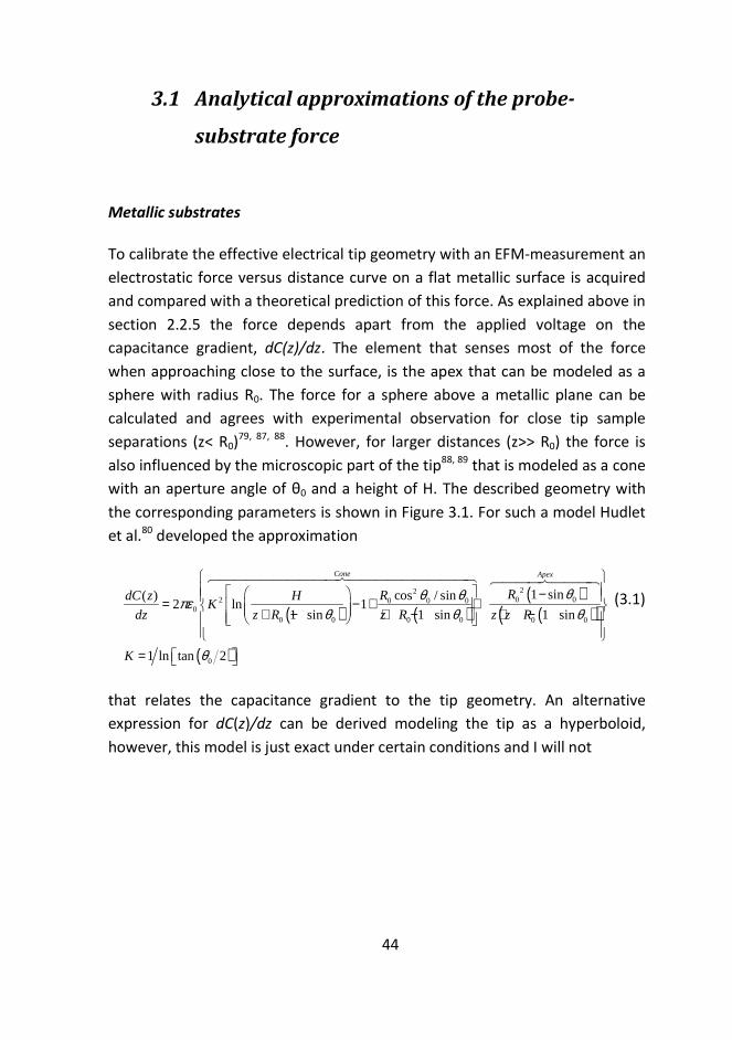
To calibrate the effective electrical tip geometry with an EFM-measurement an
electrostatic force versus distance curve on a flat metallic surface is acquired
and compared with a theoretical prediction of this force. As explained above in
section 2.2.5 the force depends apart from the applied voltage on the
capacitance gradient, dC(z)/dz. The element that senses most of the force
when approaching close to the surface, is the apex that can be modeled as a
sphere with radius R0. The force for a sphere above a metallic plane can be
calculated and agrees with experimental observation for close tip sample
separations (z< R0)79, 87, 88
. However, for larger distances (z>> R0) the force is
also influenced by the microscopic part of the tip88, 89
that is modeled as a cone
with an aperture angle of θ0 and a height of H. The described geometry with
the corresponding parameters is shown in Figure 3.1. For such a model Hudlet
et al.80
developed the approximation
( ) ( )( )
( )( )
( )
220 02 0 0 0
00 0 0 0 0 0
0
1 sincos / sin( )2 ln 1
1 sin 1 sin 1 sin
1 ln tan 2
Cone Apex
RRdC z HK
dz z R z R z z R
K
θθ θπεθ θ θ
θ
− = − + + + − + − + −
=
��������������������� ���������
(3.1)
that relates the capacitance gradient to the tip geometry. An alternative
expression for dC(z)/dz can be derived modeling the tip as a hyperboloid,
however, this model is just exact under certain conditions and I will not
3. Quantitative Electrostatic Force Microscopy
45
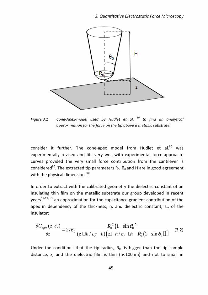
Figure 3.1 Cone-Apex-model used by Hudlet et al. 80
to find an analytical
approximation for the force on the tip above a metallic substrate.
consider it further. The cone-apex model from Hudlet et al.80
was
experimentally revised and fits very well with experimental force-approach-
curves provided the very small force contribution from the cantilever is
considered90
. The extracted tip parameters R0, θ0 and H are in good agreement
with the physical dimensions90
.
In order to extract with the calibrated geometry the dielectric constant of an
insulating thin film on the metallic substrate our group developed in recent
years17-19, 91
an approximation for the capacitance gradient contribution of the
apex in dependency of the thickness, h, and dielectric constant, εr, of the
insulator:
( )( )( )
20 0
00 0
( , ) 1 sin2
( / ) / 1 sinapex r
r r
C z R
z z h h z h h R
ε θπε
ε ε θ∂ −
=∂ + − + − + −
(3.2)
Under the conditions that the tip radius, R0, is bigger than the tip sample
distance, z, and the dielectric film is thin (h<100nm) and not to small in
46
diameter (h<<D, D>R0) equation (3.2) can be used to extract information about
the dielectric constant. This is shown in detail in chapter 4 for two different
types of thin film insulators. In other cases a modified version of equation (3.2)
can be derived (see sections 4.7.3 – 4.7.4) or finite element simulations should
be applied.
Insulating substrates
Depending on the sample under study not always metallic substrates can be
used to measure the sample of interest. In these cases, nevertheless, it is
possible to measure an electrostatic force. However, approximating the
electrostatic forces acting on the AFM-tip above the insulating substrate is
more challenging than in the case of metallic substrate and only a small
number of works trying to engage this issue have been published until now 85,
86, 92. One main difference with respect to metallic substrates is that the local
electric field lines from the apex are indirectly influenced by the macroscopic
parts of the AFM-tip (cone and cantilever). Chapter 5 will summarize the work
to reach a methodology to quantify the local dielectric constant of thick
insulating substrates that enables quantitative dielectric measurements of
samples on dielectric substrates.
3. Quantitative Electrostatic Force Microscopy
47
3.2 Finite Element Method (FEM): Introduction
into electrostatic modeling with Comsol
Multiphysics™
Most problems in physics that consider slightly more complex geometries have
no analytical solution and approximations are only valid in very limited ranges.
Therefore, one has to restore to numerical methods. This is also the case for
the electrostatic problem of the AFM-tip above the dielectric sample and
substrate I was dealing in my work.
The numerical method I applied in all my work is the Finite Element Method
(FEM), a simulation method that is especially powerful for geometrical models
involving irregular shapes and curved surfaces. It solves the partial differential
equation (PDE) of interest on as many points as necessary in the defined
geometry. For the electrostatic problem of the AFM-tip in air above the
substrate this is the Poisson Equation. The result of this calculation is for each
point of the geometry the potential, V, and the electric field, E, that can be
used to calculate for example the electrostatic force on the AFM-tip. Important
to mention, the points where V and E get calculated are defined in a meshing
step. A particular aspect of FEM is that the shape of mesh elements is
triangular (or tetrahedral in 3D) so that the specific geometry can be followed
much better than with other methods.
Beside in science, applications of FEM are also found in the field of engineering
where sometimes complex three-dimensional geometries are involved. FEM is
a computational intensive method that requires, depending on the specific
problem, beside CPU-time also big amounts of RAM (in this case at least 4 GB).
To do all the simulation in the work I present here, I used the commercially
available FEM-software Comsol Multiphysics™ that has a very user-friendly
graphical interface to define the geometry and run the simulations, but works
also with a scripting language in conjunction with Matlab™ when more specific
and repetitive simulations are required.
48
To perform a finite element simulation of a particular problem, usually the
following steps are followed:
1. The geometry is defined by drawing the sub-domains.
2. Boundary conditions are defined on the borders of the sub-domains.
3. Electric properties in the domains are defined.
4. A mesh is generated refining especially the mesh elements where
the gradient of the electrical potential is high in order improve the
quality of the solution.
5. The electrostatic problem is solved to obtain V and E. Usually V is
plotted to see the quality of the solution.
6. The quantity of interest is calculated. For the case of the
electrostatic force, the Maxwell-Stress-Tensor is integrated over the
whole tip surface.
To reduce the calculation effort, it is sensible to make use of existing
symmetries in the geometry that is calculated. For the model of the AFM-tip
above the substrate I assumed like in the derivations of Hudlet et al.80
, that the
tip is a cone and axis-symmetric with the z-axis. The simulations can be run in
2D-mode then. To give a practical idea of the simulation results I show in
Figure 3.2 a plot of the solved model (colors are the potential).
The symmetry-axis is on the left and the tip consisting of apex, cone and
cantilever is located just a few nanometers above the substrate. The insets
show the defined mesh (above) especially refined on the surface of the tip, a
zoom onto the edges of the cantilever (middle) with rounded edges to make
an accurate calculation of the electrostatic force on these boundaries possible
and a zoom onto the tip-apex (bottom). Notice, to make the simulation more
realistic the inner domain is enclosed by outer domains that use the infinite
elements function to effectively transform the position of the outer
boundaries to infinity.
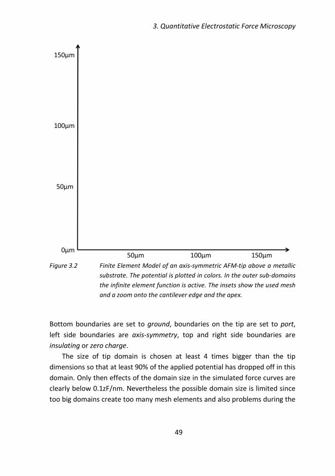
3. Quantitative Electrostatic Force Microscopy
49
150µm
100µm
50µm
0µm50µm 100µm 150µm
Figure 3.2 Finite Element Model of an axis-symmetric AFM-tip above a metallic
substrate. The potential is plotted in colors. In the outer sub-domains
the infinite element function is active. The insets show the used mesh
and a zoom onto the cantilever edge and the apex.
Bottom boundaries are set to ground, boundaries on the tip are set to port,
left side boundaries are axis-symmetry, top and right side boundaries are
insulating or zero charge.
The size of tip domain is chosen at least 4 times bigger than the tip
dimensions so that at least 90% of the applied potential has dropped off in this
domain. Only then effects of the domain size in the simulated force curves are
clearly below 0.1zF/nm. Nevertheless the possible domain size is limited since
too big domains create too many mesh elements and also problems during the
50
meshing of the very small apex (degenerated triangles or cavities are
generated).
The mesh-size on the tip-boundaries was set to 20 nm, except from the apex
where the mesh size was set to the size of the tip radius R divided by 20. The
global mesh quality was set to extra fine.
To obtain the electrostatic force o the AFM-tip the Maxwell-Stress-Tensor in z
direction was integrated over the whole tip geometry following the equation:
2
02 21
(4
( )2
1)z r ar z r z r z cE E n EF VE nε ε ⋅ ⋅ + − ⋅ ⋅= (3.3)
where n represents the respective normal vector. In Comsol-electrostatics
mode this equation reads:
Maxwell=1/2*pi*r*((Vr*VVz*nr+0.5*(Vz^2Vr^2)*nz)*epsilon0_emes)*epsilonr_emes
Vr=-nr*(lm1)/r/(epsilon0_emes*epsilonr_emes)
Vz=-nz*(lm1)/r/(epsilon0_emes*epsilonr_emes)
To improve accuracy the variable lm1 defined on the boundaries and derived
from the weak constraints is used to calculate the electric field Vr and Vz.
3. Quantitative Electrostatic Force Microscopy
51
3.2.1 A ready tool for standardized electric tip calibration
using finite element simulations
In order to quantify the dielectric image of the sample with EFM I used the
following procedure:
1. A normal topography image is acquired in dynamic or tapping mode.
2. A dC/dz-image is acquired scanning the sample again a few tens of nm
out of contact and at a defined constant height above the flat
substrate.
3. Since the dC/dz signal depends not only on the sample dielectric
constant, but also on the probe geometry the AFM-tip has to be
calibrated by a dC/dz-approach curve onto the bare metallic substrate.
4. The tip geometry is calibrated in a fitting procedure as detailed below
and the dielectric image is calculated with the tip geometry, the
acquired topography and the dC/dz image.
Since the tip geometry is a very important parameter it is advisable to repeat
the tip calibration from time to time.
As mentioned, in order to perform a quantitative extraction of the dielectric
constant, εr, of a sample it is necessary to calibrate tip-geometry in a first step.
In such a calibration procedure a theoretical expression is fitted to the
experimental dC(z)/dz-curve giving the best fitting geometric parameter R0 and
θ0 and corresponding error bounds. For the case of metallic substrates this
theoretical expression can be an analytical approximation as shown in section
52
3.1. However, as mentioned for insulating substrates and more specific sample
geometries no analytical expressions are available and the alternative
approach is to use finite element simulations. Unfortunately, one of the big
shortcomings of finite element simulations is that they give just the solution
for one specific set of parameters (e.g. one tip geometry, one tip substrate
distance z). In consequence they are not very flexible and easy to use
compared with analytical expressions.
To provide, however, a methodology capable to calibrate the tip geometry for
measurements on dielectric substrates my approach was to:
1. Simulate a large number tip-sample geometries covering the whole
range of possible parameters (apex radius R=1-120nm, cone angle
θ=5-44°, cone height H=5-20 µm, cantilever width L=0-70 µm,
substrate dielectric constant εr=2-10). The simulations had to be very
precise and fast at the same time to finish in a finite time (e.g. 1
month).
2. Generate a 5-dimensional interpolation function Force(H, L, R, Q, εr) as
a fitting function on non-linear grid.
3. Write a script capable to perform a fitting procedure with the
generated interpolation function to put out the desired parameters.
The large set of simulations was performed with Comsol™ using the scripting
in Matlab™. The total number of simulations performed for one interpolation
function is around 500.000.
The final calibration tool performing the interpolation and fitting is written in
Mathematica™. The tool works successfully and is used by the group for the
electrical tip calibration. Further details are described in chapter 5.
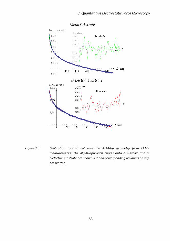
3. Quantitative Electrostatic Force Microscopy
53
Figure 3.3 Calibration tool to calibrate the AFM-tip geometry from EFM-
measurements. The dC/dz-approach curves onto a metallic and a
dielectric substrate are shown. Fit and corresponding residuals (inset)
are plotted.

4. Quantitative dielectric constant measurement of supported
biomembranes by DC-EFM
55
4 Quantitative dielectric constant measurement
of supported biomembranes by DC-EFM
4.1 Abstract
A simple method to measure the static dielectric constant of supported
biomembranes with nanometric spatial resolution is presented. The dielectric
constant is extracted from DC electrostatic force measurements with the use
of an accurate analytical model. The method is validated here on thin silicon
dioxide films (8 nm thick, dielectric constant ~ 4) and Purple Membrane
monolayers (6 nm thick, dielectric constant ~2), providing results in excellent
agreement with those recently obtained by nanoscale capacitance microscopy
using a current-sensing approach. The main advantage of the force-detection
approach resides in its simplicity and direct application on any commercial
atomic force microscope with no need of additional sophisticated electronics,
thus being easily available to researchers in materials science, biophysics and
semiconductor technology.
This chapter reproduces almost literally the article: Quantitative dielectric constant
measurement of thin films by DC electrostatic force microscopy, Nanotechnology 20, 395702
(2009) by G. Gramse, I. Casuso, J. Toset, L. Fumagalli and G. Gomila.
In this article I was in charge of performing the experiments, the theoretical modeling and
processing the results. In this part of the work I followed suggestions in the experimental
methodology by I. Casuso and L.Fumagalli and in the theoretical part by J. Toset and my
supervisor. The article was written by me with the collaboration of my supervisor and the senior
researcher L. Fumagalli.
56
4.2 Introduction
As we mentioned in the introduction, probing the nanoscale dielectric
constant of biomembranes is fundamental in biology, because many
bioelectric processes depend on the value of this property at the nanoscale 93
.
Since standard characterization techniques are not capable of addressing the
dielectric constant of biomembranes at this scale, new techniques are needed
to achieve higher spatial resolution.
The large number of electrical scanning force microscopy (SFM) techniques
applied in recent years to study electrostatic and dielectric properties of
nanostructures and thin films both at low and high frequency 11, 12, 15, 17-20, 32, 38,
69, 70, 82, 83, 94-103 still present some fundamental problems. In particular, the long
range nature of the electrical interaction and the complexity of the tip-sample
geometry, make the accurate modelling of experimental data and hence the
correct quantification of the dielectric properties rather difficult.
For thin dielectric films this difficulty has been recently overcome by the
derivation of a simple analytical model that accurately quantifies the tip-thin
film capacitance 18
. Applying this model to local capacitance measurements
obtained with a current-sensing nanoscale capacitance microscope 15, 20
the
precise quantification of the low-frequency dielectric constant of thin silicon
dioxide films 17
and supported biomembranes 19
has been successfully
achieved at the nanoscale. However, current-sensed dielectric microscopy on
ultrathin films has the drawback of requiring an extremely sensitive
instrumentation (sub-attoFarad capacitance resolution) that is usually not
available with commercial SFM.
In this work we adapted the method and analytical model validated
with the current-sensing approach to DC electrostatic force microscopy (DC
EFM) and provide a simple measurement approach for supported
biomembranes and thin dielectric films in particular, using standard SFM. We
will show that, in spite of its simplicity, the DC force-detection based approach
4. Quantitative dielectric constant measurement of supported
biomembranes by DC-EFM
57
can provide quantitative values of the static dielectric constant of supported
biomembranes and thin films at the nanoscale with a performance comparable
(or better) to nanoscale capacitance measurements. In particular, we will show
that for ultrathin films (thickness <10 nm) and low dielectric constant materials
(εr <10), a precision below ~5% and a spatial resolution better than ~70 nm can
be easily obtained with a commercial atomic force microscope (AFM) with no
need of any additional electronic instrumentation.
58
4.3 Theoretical model and measurement protocol
Let us consider a conductive AFM probe positioned above the dielectric film of
the thickness h with the tip apex separated by an initial distance z0 from the
conductive substrate, as schematically shown in Figure 4.1. When a DC voltage
is applied between the probe and the substrate, the cantilever deflects by an
amount D, yielding a new equilibrium position of the apex at a distance
0z z D h= − − from the thin film. The deflection D depends on the spring
constant k of the cantilever, the potential difference between tip and sample
(the applied voltage V reduced by the surface potential VSP) and the total
capacitance CT between the probe and the sample, according to the relation
( )2
0
1
2T
SP
CD z h z V V
k z
∂≡ − − = − −∂
(4.1)
The Van der Waals interaction has not been included, since it is negligible at
the tip-substrate distance considered here (tens of nanometers).
The total probe-sample capacitance CT can be modelled as the sum of two
contributions, the stray capacitance Cstray given by the micrometric
components of the probe (cone and cantilever) and the apex contribution,
Capex. The apex capacitance, Capex, depends on the local properties of the
sample and for thin dielectric films, it can be modelled using the formula
already experimentally validated by nanoscale capacitance microscopy and
finite-element numerical simulations 17
02 ln 1 ( , )apexr
RC R K R
z hπε θ
ε
= + + +
ɶ (4.2)
where (1 sin )R R θ= −ɶ , ε0 is the vacuum permittivity, εr the relative dielectric
constant, h the film thickness, R the apex radius, θ an angle defining the apex
surface (typically the cone angle) and K is an irrelevant constant term
depending on the tip geometry. This model is valid for smooth surfaces with
topography variations with a lateral spatial variation longer than the spatial
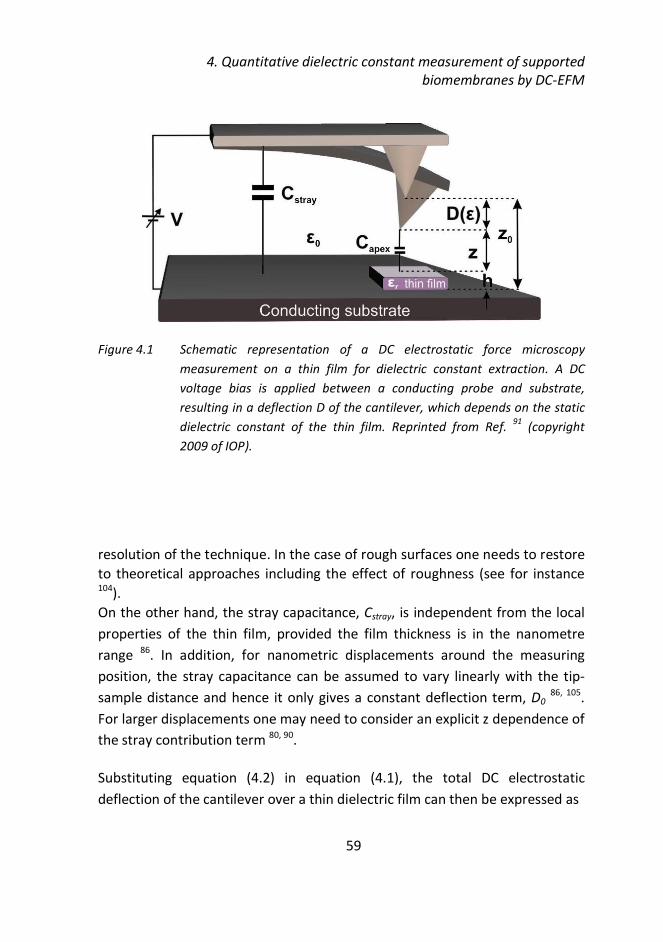
4. Quantitative dielectric constant measurement of supported
biomembranes by DC-EFM
59
Figure 4.1 Schematic representation of a DC electrostatic force microscopy
measurement on a thin film for dielectric constant extraction. A DC
voltage bias is applied between a conducting probe and substrate,
resulting in a deflection D of the cantilever, which depends on the static
dielectric constant of the thin film. Reprinted from Ref. 91
(copyright
2009 of IOP).
resolution of the technique. In the case of rough surfaces one needs to restore
to theoretical approaches including the effect of roughness (see for instance 104
).
On the other hand, the stray capacitance, Cstray, is independent from the local
properties of the thin film, provided the film thickness is in the nanometre
range 86
. In addition, for nanometric displacements around the measuring
position, the stray capacitance can be assumed to vary linearly with the tip-
sample distance and hence it only gives a constant deflection term, D0 86, 105
.
For larger displacements one may need to consider an explicit z dependence of
the stray contribution term 80, 90
.
Substituting equation (4.2) in equation (4.1), the total DC electrostatic
deflection of the cantilever over a thin dielectric film can then be expressed as
60
( )2 10
0SP
r r
V V RR h hD z R z Dk
πεε ε
−− = + + + +
ɶɶ (4.3)
Equation (4.3) constitutes a generalization to larger tip-sample distances of the
expression proposed by Sacha et al.85
In addition for metallic samples, since
0→rh ε , equation (4.3) reduces to the well known formula by Hudlet et al. 80
( ) ( )2
10
0SPV V RR
D z R z Dk
πε −− = + ⋅ +
ɶɶ (4.4)
Equation (4.3) can be solved to express the dielectric constant as a function of
the cantilever deflection,
{ ( ) ( )( )
112 2
2 0
0
( ) 2 2 2 4 4 SPr
V V RRD h z R z R z z R
k D D
πεε
−−
− = − − + + − + + −
ɶɶ ɶ ɶ (4.5)
Note that, in order to express equation (4.5) in terms of measurable
quantities, the tip - sample distance z should be substituted with z0 − D − h.
Equation (4.5) provides a simple analytical expression that can be used to
reconstruct quantitative maps of the dielectric constant from static EFM
images. We will practically demonstrate this here by implementing a protocol
similar to the one used in Ref. 19
for current-detected dielectric measurements.
After taking the topography of the thin film in dynamic mode to obtain its
thickness h, the tip is retracted out-of-contact at a distance z0 above the
substrate and scanned at constant-height with a DC applied voltage while the
cantilever deflection is recorded, as shown in Figure 4.2.
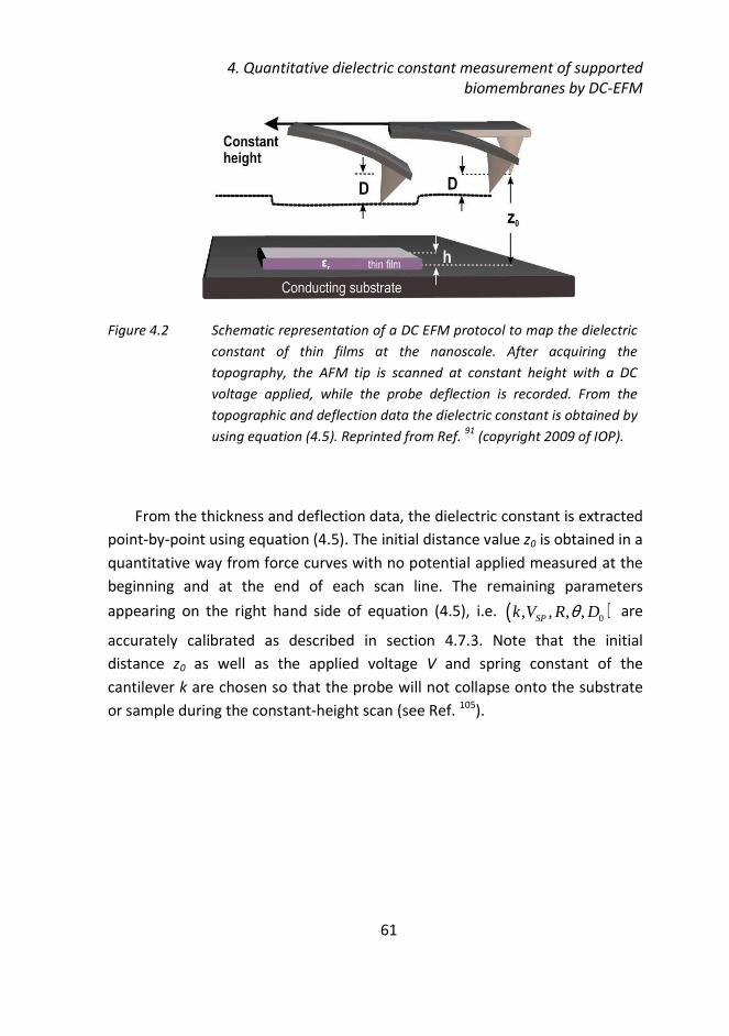
4. Quantitative dielectric constant measurement of supported
biomembranes by DC-EFM
61
Figure 4.2 Schematic representation of a DC EFM protocol to map the dielectric
constant of thin films at the nanoscale. After acquiring the
topography, the AFM tip is scanned at constant height with a DC
voltage applied, while the probe deflection is recorded. From the
topographic and deflection data the dielectric constant is obtained by
using equation (4.5). Reprinted from Ref. 91
(copyright 2009 of IOP).
From the thickness and deflection data, the dielectric constant is extracted
point-by-point using equation (4.5). The initial distance value z0 is obtained in a
quantitative way from force curves with no potential applied measured at the
beginning and at the end of each scan line. The remaining parameters
appearing on the right hand side of equation (4.5), i.e. ( )0, , , ,SPk V R Dθ are
accurately calibrated as described in section 4.7.3. Note that the initial
distance z0 as well as the applied voltage V and spring constant of the
cantilever k are chosen so that the probe will not collapse onto the substrate
or sample during the constant-height scan (see Ref. 105
).
62
4.4 Validation of the method
We validate the method on two different samples, a silicon dioxide thin
film and a supported biomembrane, namely Purple Membrane (PM). The Si02
thin film has been deposited on a flat gold substrate in the form of a squared
pattern by using Focused Ion Beam (FIB) deposition. The Si02 square has the
nominal dimensions (length x width x height) = (6 μm x 6 μm x 8 nm).
The Purple Membrane has been obtained by isolation from Halobacterium
Salinarum following standard procedures 106
. The membrane patches with
typical diameters below 1 µm and thickness around 6 nm have been adsorbed
on a highly ordered pyrolytic graphite (HOPG) substrate by placing a drop of
PM solution (concentration of 0.1mM in MilliQ water) under an electric field of
approximately 10V/cm for ~3 min. Subsequently the sample was rinsed gently
and dried under dry N2 flow.
We used a commercial AFM (Nanotec Electrónica S.L, Spain) controlled
with the WSxM software. Two types of conductive probes were employed: the
Pt-Ir coated tips on the Si02 sample (SCM-PIT-20, Nanoworld®, nominal spring
constant k = 2.8 N/m) and boron-doped diamond tips on the PM sample (CDT-
FMR, Nanosensors, nominal spring constant k = 2.8 N/m). Spring constant of
medium values were chosen as a trade-off between force sensitivity and snap-
in distance under a DC applied voltage 105
, as discussed in section 4.5. All the
measurements reported in this session were carried out at ambient conditions
with 10 V applied.
4. Quantitative dielectric constant measurement of supported
biomembranes by DC-EFM
63
4.4.1 Nanoscale dielectric constant measurement on a thin
SiO2 film
A topographic image and profile of the SiO2 thin film, obtained with the Pt-Ir
tip is shown in Figure 4.3A. The SiO2 film shows the nominal thickness of ~8nm
except at the edges where it is higher due to the deposition process. Figure
4.3B shows the corresponding deflection profile obtained by scanning the
probe above the sample at an initial tip-substrate distance z0 ~ 36nm with 10 V
applied. The measured cantilever deflection profile displays a striking
resemblance to the topography profile shown in Figure 4.3A, indicating both
the sensitivity and locality of force-detected dielectric measurements.
Figure 4.3C shows the dielectric constant calculated using equation (4.5) from
the profiles given in Figure 4.3A and Figure 4.3B on the central points of the
scan line where the dielectric film is ~8nm thick. The calibrated parameters
used in the calculation are: VSP,substrate= 0.04V, VSP,sample= 0.15V, R = 87nm, k =
2.5N/m and D0,Si02 ~ −3.7 nm (see section 4.7.1 for calibration details).
The obtained dielectric constant values display the statistical distribution
shown in the histogram in figure 3D with a mean value of εr,Si02=4.0 ± 0.9 and
the error corresponding to one standard deviation.
It is worth remarking that the uncertainty in the dielectric constant σε~ 0.9 is
consistent with the noise present in the deflection detection system (σ∆ ~ 0.1
nm) as computed from the relationship σε ∼ D∂
∂ε σ∆ (see section 4.7.2 for
statistical details). This indicates that the main source of uncertainty in the
present measurements comes from the deflection detector noise. The
obtained dielectric constant is well in agreement with values reported in the
literature for bulk samples (fused silica εr = 3.8) 107
and for similar thin SiO2
films measured at the nanoscale by nanoscale capacitance microscopy (εr ~ 4) 17
.
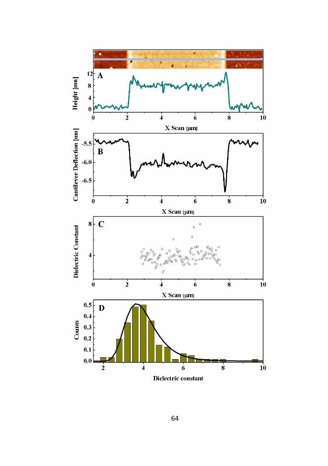
64
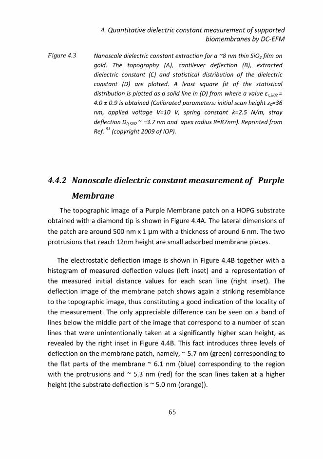
4. Quantitative dielectric constant measurement of supported
biomembranes by DC-EFM
65
Figure 4.3 Nanoscale dielectric constant extraction for a ~8 nm thin SiO2 film on
gold. The topography (A), cantilever deflection (B), extracted
dielectric constant (C) and statistical distribution of the dielectric
constant (D) are plotted. A least square fit of the statistical
distribution is plotted as a solid line in (D) from where a value εr,Si02 =
4.0 ± 0.9 is obtained (Calibrated parameters: initial scan height z0=36
nm, applied voltage V=10 V, spring constant k=2.5 N/m, stray
deflection D0,Si02 ~ −3.7 nm and apex radius R=87nm). Reprinted from
Ref. 91
(copyright 2009 of IOP).
4.4.2 Nanoscale dielectric constant measurement of Purple
Membrane
The topographic image of a Purple Membrane patch on a HOPG substrate
obtained with a diamond tip is shown in Figure 4.4A. The lateral dimensions of
the patch are around 500 nm x 1 µm with a thickness of around 6 nm. The two
protrusions that reach 12nm height are small adsorbed membrane pieces.
The electrostatic deflection image is shown in Figure 4.4B together with a
histogram of measured deflection values (left inset) and a representation of
the measured initial distance values for each scan line (right inset). The
deflection image of the membrane patch shows again a striking resemblance
to the topographic image, thus constituting a good indication of the locality of
the measurement. The only appreciable difference can be seen on a band of
lines below the middle part of the image that correspond to a number of scan
lines that were unintentionally taken at a significantly higher scan height, as
revealed by the right inset in Figure 4.4B. This fact introduces three levels of
deflection on the membrane patch, namely, ~ 5.7 nm (green) corresponding to
the flat parts of the membrane ~ 6.1 nm (blue) corresponding to the region
with the protrusions and ~ 5.3 nm (red) for the scan lines taken at a higher
height (the substrate deflection is ~ 5.0 nm (orange)).
66
Figure 4.4C displays the reconstructed dielectric constant image together
with the histogram of values on selected areas (inset). The image values have
been computed by using equation (4.5) with the deflection and topography
image given in Figures 4.4A and 4.4B, including the initial distance values
shown on the right inset of Figure 4.4B. The calibrated parameters used in the
calculation are in this case: k = 3 N/m, R = 167 nm, VSP,substrate=0.01V,
VSP,PM=0.11V and D0,PM ~ −0.5 nm (see Appendix 1). The values of the dielectric
constant obtained on a flat region of the membrane (squared area I in figure
4.4C) follow the statistical distribution shown in the inset of Figure 4.4C, with
mean εr,I=1.78 ± 0.07. This value is in good agreement with the value recently
obtained on a similar sample by means of nanoscale capacitance microscopy
(εr= 1.9 ± 0.1) 19
. Again, the standard deviation of the dielectric constant
(σε~0.07) is consistent with the deflection detection noise (σD~0.06 nm)
displayed by the measuring system. This shows that even when different scan
lines are involved in the calculations, the main source of noise continues to be
the deflection detection noise.
It is worth remarking that the obtained dielectric constant value is
insensitive to the scan height provided its value is recorded precisely as we did
here, thus showing the robustness of the present method. This can be
observed by the fact that the dielectric constant value extracted in the area II
in Figure 4C scanned at a different scan height, εr,II=1.82±0.06, agrees with the
value extracted in area I, εr,I=1.78±0.07.
Figure 4.4 Nanoscale dielectric constant measurement on a Purple Membrane
patch. The topography (A), the cantilever deflection (B) and the
extracted dielectric constant (C) are displayed. In the right inset in B the
simultaneously acquired lift height is plotted for each line. Histograms in
the inset of B and C show the distribution of the cantilever deflection and
the dielectric constant on the purple membrane, respectively. (Calibrated
parameters: applied voltage V=10V, spring constant k=3.0 N/m, stray
deflection D0,PM ~ −0.5 nm and apex radius R=167nm). Reprinted from Ref. 91 (copyright 2009 of IOP).
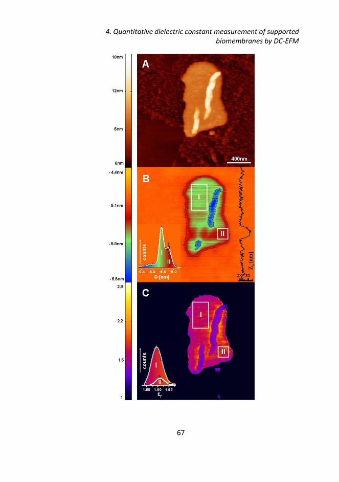
4. Quantitative dielectric constant measurement of supported
biomembranes by DC-EFM
67
68
Finally, we note that the dielectric constant obtained at the edges or
on the nanometric protrusions of the membrane is slightly smaller (εr ~1.5)
and exceeds the experimental error obtained on the flat regions. This is
probably due to the fact that the model is only valid on flat thin films larger
than the spatial resolution of the technique, whereas the size of the
protrusions is at or below the resolution limit. In the present case the lateral
resolution can be estimated to be ~80 nm, defined as half the distance needed
for the deflection to pass from the average value on the bare substrate to that
on the flat membrane region (data not shown). This value is in good
agreement with the theoretical lateral resolution of the technique 108
~
0 70Rz nm≈ .
4. Quantitative dielectric constant measurement of supported
biomembranes by DC-EFM
69
4.5 Discussion
In the previous section we have shown the ability of DC EFM to quantify the
static dielectric constant of two different thin films at the nanoscale. Here we
will analyze the factors that determine the uncertainty of the extracted values
and establish the best application range of the technique.
According to the results reported in Section 4.4 the uncertainty of the
dielectric constant value, represented by the standard deviation of values, σε,
is mainly determined by the deflection detection noise of the AFM system, σD,
through the relationship σε ∼ D∂
∂ε σD. Several parameters appear in this
equation, which can play a role in the final standard deviation of dielectric
constant σε. In order to illustrate the most relevant factors, we will consider
the case of the measurement performed on the Purple Membrane patch. By
taking as initial parameters those of the experiment, namely, k=3 N/m, V=10 V,
εr=2, z0=30 nm, h=6 nm, R=167 nm, we will analyze how the uncertainty of the
measurement evolves when varying each of them individually, while keeping
the others fixed. In each case, three levels of deflection detection noise will be
considered, namely, σD = 0.06 nm, 0.03 nm and 0.01 nm, corresponding,
respectively, to the noise of our setup, of a state-of-the-art commercial AFM
and to further optimized AFM for static measurements.
Figure 4.5 shows the predicted variation for the relative error in the dielectric
constant as a function of (a) initial scan height, (b) applied voltage, (c) spring
constant, (d) apex radius (lateral resolution), (e) relative dielectric constant of
the material and (f) film thickness. In each case the parameters are varied in a
range satisfying the condition that the tip does not collapse onto the sample.
Figure 4.5 reveals a rather different impact of each parameter on the
uncertainty of the measurement.
Explicitly, for the present case, the relative error depends in each case
roughly as: ~z0β
(β=1-2), ~V−2
, ~ k
1, ~R
−α (α=1-2), ~ εr
1, ~h
−γ (γ=1-2).
According to these results, for a given instrumental detection noise, the
70
precision of the measurement can be greatly increased by reducing the scan
height and spring constant, and by increasing the applied voltage, as expected.
However, the condition that the probe does not collapse onto the sample or
substrate imposes a trade-off between these parameters. Since the collapse
distance does not depend on the spring constant of the cantilever but on the
voltage at which the electrostatic collapse occurs 105
, it turns out that
intermediate spring constant cantilevers (k~1-10 N/m) are expected to provide
the best results, since softer cantilevers would not allow applying large enough
voltages, while stiffer cantilevers would produce deflection values below the
deflection noise of the instrument.
On the other hand, by increasing the spatial resolution (decrease in the apex
radius) a large increase in the uncertainty of the measurement is observed.
This means that also here a trade-off should be made between spatial
resolution (apex radius) and dielectric constant precision.
Concerning the parameters of the thin film, εr and h, the relative error
increases linearly with εr and decreases slightly faster with h. This means that
in principle increasing the sample thickness could constitute a good strategy to
increase the precision of the measurement. However, this is not the case in
practice since only slight variations of this parameter are allowed without the
need to increase the scanning height, which will result in an overall decrease
of precision.
Therefore, the best results will be obtained in the ultrathin limit (<10 nm), with
a precision still acceptable in the molecularly thin (<2 nm) or thicker limits (>10
nm). In all the cases, since the uncertainty increases linearly with the dielectric
constant of the material, measurements will be significantly more precise on
low dielectric constant materials (εr<10) than in higher dielectric constant
materials. The increase in the uncertainty with increasing dielectric constant
value is a consequence of the fact that the measurement is not performed in
contact with the sample. In this condition the applied potential partitions
between the air gap and the thin film in such a way that the interaction
between probe and thin film gets remarkably less sensitive to the dielectric
constant of the material than expected from contact measurements.
According to the above discussion, the present technique is expected to be
4. Quantitative dielectric constant measurement of supported
biomembranes by DC-EFM
71
best suited for ultrathin films (h<10 nm) and low dielectric constant materials
(εr<10). For these thin films, if an appropriate trade-off between the different
parameters and measuring conditions is achieved, dielectric constant values
with relative errors well below ~5% and a spatial resolution below ~70 nm can
be obtained with a commercial AFM system.
Higher spatial resolution can be achieved at the cost of precision, unless the
deflection detection noise of the system is reduced. To this end, besides
instrumental optimization, one can reduce the experimental noise by
increasing the measurement time and averaging a number of identical
measurements. Further improvements can only be achieved by moving to a
more sensitive detection scheme such as alternating applied voltage EFM (AC-
EFM), which however requires additional instrumentation (i.e. lock-in
amplifier) not always available with standard AFM.
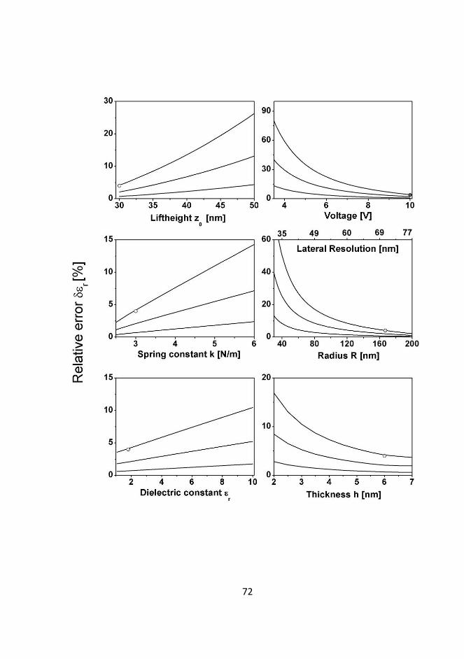
72
4. Quantitative dielectric constant measurement of supported
biomembranes by DC-EFM
73
Figure 4.5 Relative error of εr as a function of (a) initial scan height, (b)
voltage applied, (c) spring constant, (d) apex radius (lateral
resolution), (e) relative dielectric constant of the material and (f)
film thickness. In each figure three levels of noise are considered
(from top to bottom): σD=0.06 nm, 0.03 nm and 0.01 nm. The
remaining parameters are k=3 N/m, V=10 V, εr=2, z0=30 nm, h=6
nm, R=166 nm, θ=30°, D0=0.5nm and VSP=0.1V. In each figure the
symbol corresponds to the experimental conditions of the purple
membrane experiments reported here. Reprinted from Ref. 91 (copyright 2009 of IOP).
74
4.6 Conclusion
In this chapter we have demonstrated a simple methodology based on DC
electrostatic force microscopy to obtain quantitative values of the static
dielectric constant of supported biomembranes and thin insulating films at the
nanoscale. we have shown that, in spite of its simplicity, the proposed
methodology implemented on a conventional AFM system can provide
dielectric constant values with relative errors below a 5% and spatial
resolutions below ~70 nm for ultrathin (thickness <10 nm) and low dielectric
constant materials (relative dielectric constant < 10) materials. The technique
has been validated on a ~8 nm thin SiO2 film and on a ~6 nm thin biological
membrane, with results in excellent agreement with dielectric constant values
found in the literature for bulk samples or obtained with the current-sensing
based nanoscale dielectric microscopy, recently reported. This method
constitutes a very simple approach to the measurement of nanoscale dielectric
constant on thin films as it can be implemented on virtually any commercially
available AFM with no need of additional electronics or complex numerical
simulations, thus making this technique easily accessible to researches in
material science, semiconductor technology and biophysics.
4. Quantitative dielectric constant measurement of supported
biomembranes by DC-EFM
75
4.7 Appendix
4.7.1 Parameter calibration
In order to obtain quantitative values for the dielectric constant from equation
(4.5), precise calibration of the parameters appearing in this equation is
essential.
The spring constant of the cantilever, k, has been calibrated here by
analysing the thermal oscillation of the cantilever as described in Ref. 109
. We
have obtained the values kPtIr= 2.5 ± 0.1 N/m and kdiamond= 3.0 ± 0.1 N/m for the
Pt-Ir and diamond tips, respectively.
The surface potential, VSP, was estimated by acquiring the DC deflection
while sweeping the voltage between -3V and 3V on the bare substrate as well
as on the dielectric sample at different tip-sample separations (for details see
Ref.110
). Fitting the deflection curve to a parabolic function of the voltage, the
following surface potentials where obtained: VSP,PtIr-Au= 0.04 ± 0.02V, VSP,PtIr-Si02=
0.15±0.02 V, VSP,diamond-HOPG= 0.01 ± 0.02 V, VSP,diamond-PM=0.11 ± 0.03 V.
The probe radius, R, was calibrated by measuring a deflection distance
curve on the conducting substrate with a DC voltage applied and fitting it to
equation (4.4), valid for metallic samples, with the apex radius R and stray
deflection D0 as free parameters (for the extraction of the radius the mean
spring constant values have been used, i.e. kPtIr=2.5 and kdiamond=3.0, while in
order to reduce the number of parameters in the fitting process, θ was set to
30°).
Following this procedure we obtained the values RPtIr= 87±1 nm,
D0,PtIr=−4.0 ± 0.1 nm and Rdiamond= 167±1 nm, D0,diamond= − 0.17±0.01 nm. The
goodness of the procedure is shown in Figure 4.6, showing residuals with an
almost uniform distribution (standard deviations 0.11 nm and 0.05 nm for the
PtIr and diamond probes, respectively). Note that the larger deflections on the
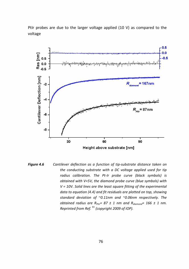
76
PtIr probes are due to the larger voltage applied (10 V) as compared to the
voltage
Figure 4.6 Cantilever deflection as a function of tip-substrate distance taken on
the conducting substrate with a DC voltage applied used for tip
radius calibration. The Pt-Ir probe curve (black symbols) is
obtained with V=5V, the diamond probe curve (blue symbols) with
V = 10V. Solid lines are the least square fitting of the experimental
data to equation (4.4) and fit residuals are plotted on top, showing
standard deviation of ~0.11nm and ~0.06nm respectively. The
obtained radius are RPtIr= 87 ± 1 nm and Rdiamond= 166 ± 1 nm.
Reprinted from Ref. 91
(copyright 2009 of IOP).
4. Quantitative dielectric constant measurement of supported
biomembranes by DC-EFM
77
applied when using the diamond probe (5 V). Note also that for the PtIr probe
the extracted radius is appreciably bigger than the nominal value. This
difference can be explained by two effects that add up for this type of probes,
namely, (i) the Pt-Ir probes can get blunt very easily, thus displaying usually a
bigger apex radius and (ii) for small radii the use of a constant stray
contribution term in equation (4.4) is less accurate thus giving rise to slightly
larger apex radius values. These two facts are not relevant for the diamond
probes and do not affect the extraction of the dielectric constant, as we have
shown.
Finally the stray deflection contribution, D0, has been quantified using
equation (4.4) for metallic samples from the deflection measured on the
conductive substrate during the scan line taken at constant-height. To reduce
the uncertainty on this parameter several deflection data obtained on the flat
substrate have been averaged out. The values obtained are then D0,Si02 ~ −3.7
nm and D0,PM ~ −0.5 nm.
4.7.2 Statistical analysis of the data
The measured deflection values display a statistical dispersion due to the
detection system noise that follows the Gaussian distribution
( )2
2
1p(D exp
22D
DD
D µσσ π
−) = −
(4.6)
where Dµ and Dσ represent the mean and standard deviation of the
distribution, respectively. Accordingly, the dielectric constant values obtained
from the deflection through the function εr(D) given in equation (4.5) are also
statistically distributed and follow the distribution
)( ) ( ) r
rr
Dp p D
εεε
∂ ( = ⋅∂
(4.7)
which in general is non-Gaussian. The mean and standard deviation values of
the dielectric constant are then given by
2( ) ; ( ) ( )r r r r r r r rp d p dεε ε ε ε σ ε ε ε ε= = −∫ ∫ (4.8)
78
In this paper we firstly obtained the distribution by fitting the histogram of
measured dielectric constant to equation (4.7) with Dµ and
Dσ as free
parameters and then calculated the mean and standard deviation using
equations (4.8). For the results reported here, it can be shown that these
values can be equivalently obtained using the approximated relation of the
non-Gaussian distribution of dielectric constant to the first order in the
deflection noise
( )2
22
( )1~
2r D
r r D DD
ε µε ε µ σ∂+∂
(4.9)
and
( )~ r D
DDεε µ
σ σ∂
∂ (4.10)
This justifies the use of equation (4.10) in the precision analysis given in
Section 4.4.
4.7.3 Analytical formula for the electrostatic force on
small AFM-tips including the cone contribution
As we mentioned in section 2.3, the formula relating the dielectric
constant with the capacitance gradient and consequently with the measured
electrostatic force is just valid under a limited number of conditions. Especially
for tips with smaller apex radii than the ones we used in this chapter, I showed
that the use of equation (3.2) can yield incorrect dielectric constant values.
This is because for small tips (R<50-100nm) not only the apex but also the cone
is contributing to the measured force-difference. I found that under these
conditions instead the following analytical equation can be used to extract the
correct dielectric constant from the measured capacitance gradient difference,
ΔC’:
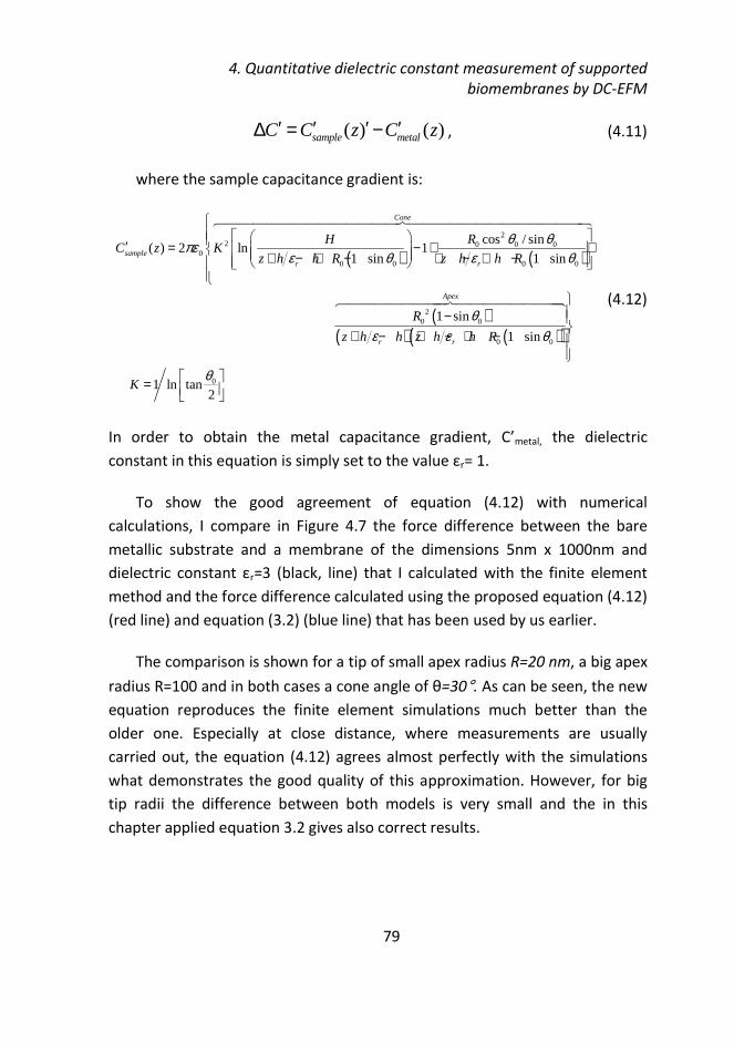
4. Quantitative dielectric constant measurement of supported
biomembranes by DC-EFM
79
( ) ( )sample metalC C z C z′ ′ ′ ′∆ = − , (4.11)
where the sample capacitance gradient is:
( ) ( )
( )( ) ( )( )
22 0 0 0
00 0 0 0
20 0
0 0
cos / sin( ) 2 ln 1
1 sin 1 sin
1 sin
1 sin
1 ln ta
Cone
sampler r
Apex
r r
RHC z K
z h h R z h h R
R
z h h z h h R
K
θ θπεε θ ε θ
θε ε θ
′ = − + + + − + − + − + −
− + − + − + −
=
�����������������������������
�������������������
0n2
θ
(4.12)
In order to obtain the metal capacitance gradient, C’metal, the dielectric
constant in this equation is simply set to the value εr= 1.
To show the good agreement of equation (4.12) with numerical
calculations, I compare in Figure 4.7 the force difference between the bare
metallic substrate and a membrane of the dimensions 5nm x 1000nm and
dielectric constant εr=3 (black, line) that I calculated with the finite element
method and the force difference calculated using the proposed equation (4.12)
(red line) and equation (3.2) (blue line) that has been used by us earlier.
The comparison is shown for a tip of small apex radius R=20 nm, a big apex
radius R=100 and in both cases a cone angle of θ=30°. As can be seen, the new
equation reproduces the finite element simulations much better than the
older one. Especially at close distance, where measurements are usually
carried out, the equation (4.12) agrees almost perfectly with the simulations
what demonstrates the good quality of this approximation. However, for big
tip radii the difference between both models is very small and the in this
chapter applied equation 3.2 gives also correct results.
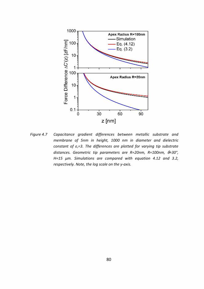
80
Figure 4.7 Capacitance gradient differences between metallic substrate and
membrane of 5nm in height, 1000 nm in diameter and dielectric
constant of εr=3. The differences are plotted for varying tip substrate
distances. Geometric tip parameters are R=20nm, R=100nm, θ=30°,
H=15 µm. Simulations are compared with equation 4.12 and 3.2,
respectively. Note, the log scale on the y-axis.
5 Quantifying the dielectric constant of thick
insulators using EFM
5.1 Abstract
This chapter deals with extending the methodology developed in the
previous chapter to the case in which thick insulating substrates, instead of
metallic substrates, are considered. As I have mentioned, the use of insulating
substrates such as glass or mica turns out to be very advantageous when
dealing with supported biomembranes. Here we present a systematic analysis
of the effects that the microscopic parts of electrostatic force microscopy
probes (cone and cantilever) have on the electrostatic interaction between the
tip apex and thick insulating substrates (thickness > 100μm). We discuss how
these effects can influence the measurement and quantification of the local
dielectric constant on thick insulating substrates. We propose and
experimentally validate a general methodology that takes into account the
influence of the cone and the cantilever, thus enabling to obtain very accurate
values of the dielectric constants on thick insulators. Finally, the locality of the
technique is discussed.
This chapter reproduces almost literally the article: "Quantifying the dielectric constant of thick
insulators by electrostatic force microscopy: Effects of the microscopic parts of the probe",
Nanotechnology 23, 205703, 2012 by G. Gramse, G. Gomila and L. Fumagalli and it includes also
a part of the article "Quantifying the dielectric constant of thick insulators using electrostatic
force microscopy", Applied Physics Letters 96, 183107, 2010, by L. Fumagalli, G. Gramse, D.
Esteban-Ferrer, M. A. Edwards, and G. Gomila. In these two articles I was in charge of
performing the theoretical modeling. In this part of the work I followed suggestions in the
modeling methodology by M. A. Edwards. The experimental data was acquired and processed by
L. Fumagalli. This part of the work was supervised jointly by the senior researcher L. Fumagalli
and my supervisor. The first article and the part of the second article reproduced here was
written in both cases by me, in collaboration with my supervisor and the senior researcher L.
Fumagalli.
82
5.2 Introduction
Measurement and quantification of the dielectric constant, εr, at the nanoscale
has been demonstrated using scanning force microscopy based on
capacitance17, 19
and electrostatic force 82, 83, 91, 102, 111, 112
detection for the case
of thin insulating films (thickness < 1μm), with examples ranging from thin
oxide films and polymer blends to supported biomembranes. On thick
insulators (thickness > 10μm), on the other hand, quantifying εr is much more
difficult, not only because the signal-to-noise ratio is smaller, but also because
the data interpretation sensitively depends on the modeling of the probe. This
is due to the fact that the geometry of the microscopic parts of the probe, that
is, the cone and the cantilever, can indirectly influence the local electrostatic
interaction between the tip apex and the thick dielectrics, as suggested by
some theoretical works 85, 86, 113, 114
. However, the ability to quantify the
dielectric constants on thick insulators would open new possibilities, such as
the study of interfacial effects of insulators 115
and thick nanocomposite
insulators 116
. Particularly, it would enable the electrical/dielectric
characterization of molecules and nano-objects (single biomolecules117
, self-
assembled monolayers38, 118
, liquid layers38
, nanotubes 119
, nanoparticles120
)
directly on millimeter-scale insulating substrates like mica or glass cover slips,
thus avoiding the difficulties in preparation on conductive substrates.
Here, we systematically analyze from a theoretical point of view the
influence of the cone height and the cantilever area on the local electrostatic
interaction between the tip apex and thick dielectric substrates and hence on
the quantification of the local dielectric constant. Based on these results, we
propose and experimentally validate a general methodology to properly
account for these effects. We show that adding a disc that simulates the
cantilever further improves the accuracy of the obtained dielectric constants.
5. Quantifying the dielectric constant of thick insulators using EFM
83
The final result is a very accurate and systematic methodology to extract the
dielectric constant of the nanometric volume at the surface of a thick
insulating material. This methodology is also readily applicable to quantitative
measurements on bio-membranes.
The chapter is organized as follows. In section 5.3 we describe the probe-
thick insulator system and the numerical approach used to solve the
corresponding electrostatic problem. In section 5.4 we analyze how the cone
and the cantilever affect the tip-substrate electrostatic interaction. In section
5.5 we investigate their influence on the obtained dielectric constant from
EFM measurements and propose a general methodology to extract the
dielectric constants on thick insulators, taking into account the microscopic
effects of the cone and cantilever. In section 5.6 we address the locality of the
technique. Finally in section 5.7 we summarize the main conclusions of this
chapter.
5.3 Theoretic Modeling
To analyze the effect of the microscopic parts of the EFM probe (the cone and
the cantilever) on the tip apex – thick insulator interaction, we considered the
simplified model given in Figure 5.1. The probe consists of a truncated cone of
height H and cone aperture angle θ ended with a semi-spherical apex of radius
R. In addition, a disc of radius and thickness w is located on top of the cone,
where L is the part of disc radius not covered by the cone base. Here, for
simplicity, we will refer to L as to the cantilever disc radius. The tip apex is
positioned at a distance z from the thick insulator substrate of dielectric
constant εr. we assume that the insulating substrate has infinite lateral and
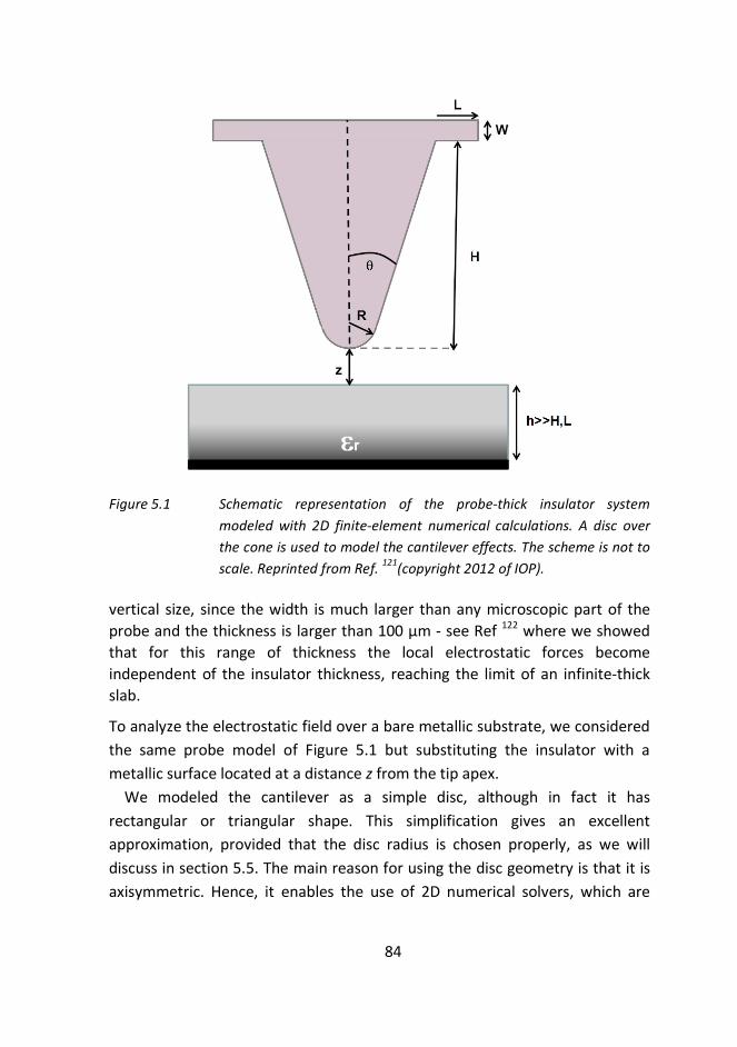
84
Figure 5.1 Schematic representation of the probe-thick insulator system
modeled with 2D finite-element numerical calculations. A disc over
the cone is used to model the cantilever effects. The scheme is not to
scale. Reprinted from Ref. 121
(copyright 2012 of IOP).
vertical size, since the width is much larger than any microscopic part of the
probe and the thickness is larger than 100 μm - see Ref 122
where we showed
that for this range of thickness the local electrostatic forces become
independent of the insulator thickness, reaching the limit of an infinite-thick
slab.
To analyze the electrostatic field over a bare metallic substrate, we considered
the same probe model of Figure 5.1 but substituting the insulator with a
metallic surface located at a distance z from the tip apex.
We modeled the cantilever as a simple disc, although in fact it has
rectangular or triangular shape. This simplification gives an excellent
approximation, provided that the disc radius is chosen properly, as we will
discuss in section 5.5. The main reason for using the disc geometry is that it is
axisymmetric. Hence, it enables the use of 2D numerical solvers, which are
5. Quantifying the dielectric constant of thick insulators using EFM
85
much faster and accurate than 3D solvers when large geometries including
nanometric features (here the apex) have to be calculated.
The electrostatic problem was solved numerically by the finite-
element package COMSOL Multiphysics 4.0 (AC /DC electrostatic module). The
infinite lateral and vertical dimensions of the simulation box (air and substrate
domain) were implemented by using the built-in infinite elements function
around an inner domain of finite size having ten times the width and height of
the largest tip dimension. Constant potential boundary conditions were
assumed on the probe surface and at the bottom of the insulating substrate
(here taken as ground), while insulating boundary conditions were used on the
lateral and upper sides of the simulation box. The calculation was done with
the direct axisymmetric 2D solver PARDISO (calculation time per point
between 6 and 10 seconds on a computer with a 2.5 GHz CPU and 4 GB RAM).
The force acting on the probe was calculated by integration of the
built-in Maxwell-stress-tensor function over the probe surface. To pass from
the 2D calculations to the 3D ones, the corresponding 2πr factor was included,
where r is the distance from the 2D probe surface to the symmetry axis. We
estimated the accuracy of our calculations to be better than 1% against the
analytical expression of the electrostatic force acting on a conducting sphere in
front of an infinite dielectric substrate 84
. To analyze the electrostatic
interaction independently of the applied potential and to get rid of non-local
contributions, the calculated force F2ω(z,εr) was converted into capacitance
gradient variations ∆C’(z,εr) = C’(z,εr) – C’(z0,εr), as we already detailed in
Ref.122
.
We systematically calculated the capacitance gradient as a function of
all the parameters, covering the range of values of interest (R = 1-120 nm,
θ=5º-40º, H = 5-20 μm, L = 0-35 μm, εr = 1-11, z = 6-800 nm, w = 2 μm) using an
automatic script (with a total computational time of 3 weeks). We then
implemented a code in Mathematica 7.0 that interpolates the calculated
values, generates two functions, corresponding to the metallic and the
dielectric substrate respectively, and finally fits them to the experimental data
with no need for further finite-element calculations.
86
5.4 Effects of the microscopic probe geometry on
the local electrostatic interaction.
The local electrostatic interaction between the probe and the thick
insulator depends on the size of the microscopic parts of the probe, and thus
on the cone height, H, and the cantilever disc radius, L. To show it, we
analyzed the capacitance gradient variation, ∆C’(z, εr), as a function of the tip-
surface distance z (approach curve) for different probes of variable size H and L
but fixed apex radius and cone angle (R = 30 nm and θ = 30°). For clarity, we
also calculated and separated the capacitance contribution of the cone,
∆C’cone(z,εr), from the contribution of the cantilever, ∆C’cant(z, εr), where
∆C’(z, εr) = ∆C’cone(z, εr)+ ∆C’cant(z, εr). For a given probe size, we calculated and
analyzed the approach curves on both metallic and insulating substrates.
5.4.1 Metallic substrates
Figures 5.2a and 5.2b show calculated approach curves, ∆C’metal(z), on a
metallic substrate for probes with variable disc radius L = 0, 10, 20 and 30 µm
for small (H = 5 µm, Figure 5.2a) and large cone heights (H = 15 µm, Figure
5.2b). Separated contributions from the cone and cantilever parts are shown in
the insets. In all cases, the cone contribution, ∆C’metal,cone(z), is independent of L
and H. This confirms the functional dependence given by the analytical
approximation derived by Hudlet et al. in Ref. 80
(dashed line in the insets of
Figure 5.2)
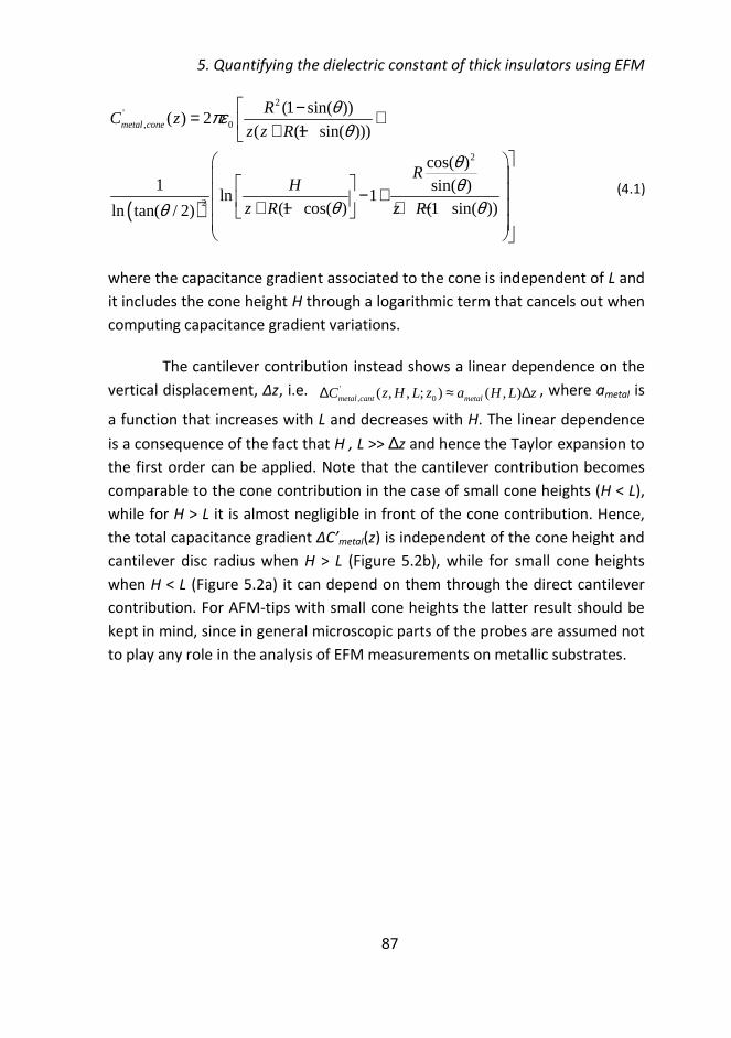
5. Quantifying the dielectric constant of thick insulators using EFM
87
( )
2'
, 0
2
2
(1 sin( ))( ) 2
( (1 sin( )))
cos( )1 sin( )
ln 1(1 cos( ) (1 sin( ))ln tan( / 2)
metal cone
RC z
z z R
RH
z R z R
θπεθ
θθ
θ θθ
−= + + −
− + + − + −
(4.1)
where the capacitance gradient associated to the cone is independent of L and
it includes the cone height H through a logarithmic term that cancels out when
computing capacitance gradient variations.
The cantilever contribution instead shows a linear dependence on the
vertical displacement, Δz, i.e. ', 0( , , ; ) ( , )metal cant metalC z H L z a H L z∆ ≈ ∆ , where ametal is
a function that increases with L and decreases with H. The linear dependence
is a consequence of the fact that H , L >> ∆z and hence the Taylor expansion to
the first order can be applied. Note that the cantilever contribution becomes
comparable to the cone contribution in the case of small cone heights (H < L),
while for H > L it is almost negligible in front of the cone contribution. Hence,
the total capacitance gradient ∆C’metal(z) is independent of the cone height and
cantilever disc radius when H > L (Figure 5.2b), while for small cone heights
when H < L (Figure 5.2a) it can depend on them through the direct cantilever
contribution. For AFM-tips with small cone heights the latter result should be
kept in mind, since in general microscopic parts of the probes are assumed not
to play any role in the analysis of EFM measurements on metallic substrates.
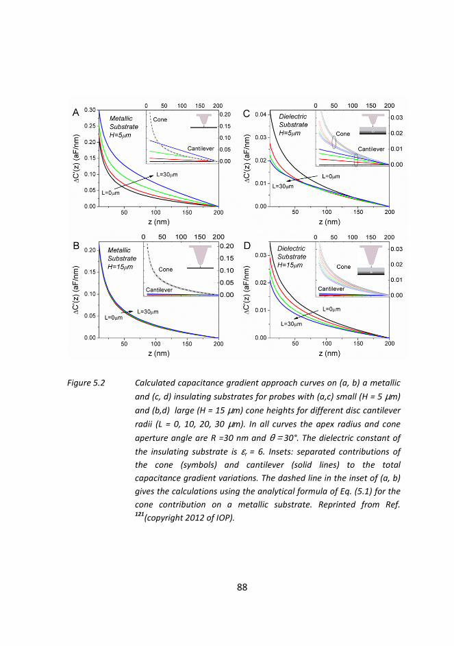
88
Figure 5.2 Calculated capacitance gradient approach curves on (a, b) a metallic
and (c, d) insulating substrates for probes with (a,c) small (H = 5 µm)
and (b,d) large (H = 15 µm) cone heights for different disc cantilever
radii (L = 0, 10, 20, 30 µm). In all curves the apex radius and cone
aperture angle are R =30 nm and θ = 30°. The dielectric constant of
the insulating substrate is εr = 6. Insets: separated contributions of
the cone (symbols) and cantilever (solid lines) to the total
capacitance gradient variations. The dashed line in the inset of (a, b)
gives the calculations using the analytical formula of Eq. (5.1) for the
cone contribution on a metallic substrate. Reprinted from Ref. 121
(copyright 2012 of IOP).
5. Quantifying the dielectric constant of thick insulators using EFM
89
5.4.2 Thick insulating substrates
Figures 5.2c and 5.2d show the capacitance gradient approach curves
calculated for the case of an insulator substrate (εr = 6), ∆C’dielec(z, εr), with the
same probe sizes considered in Figures 5.2a and 5.2b, respectively. Again, the
insets of Figures 5.2c and 5.2d show the separated contributions of the cone
and cantilever. The main difference with respect to the case of a metallic
substrate is that on a thick insulator the cone contribution, ∆C’dielec,cone(z, εr),
depends on both the cone height, H, and the disc radius, L. For a given cone
height, H, the cone contribution decreases with increasing the disc radius.
Moreover, for a given disc radius L, the cone contribution decreases
(increases) when increasing the cone height for H > L (H < L). This indicates that
the microscopic parts of the probe might have an indirect influence on the
local tip-surface interaction, thus giving such a complex behavior as
theoretically anticipated in Refs. 85, 86, 108, 113, 114
. We support this statement
with Figure 5.3, where local and non-local potential distributions are shown for
four representative probes corresponding to: (Figure 5.3a) H = 5 μm, L = 0 μm,
(Figure 5.3b) H = 15 μm, L = 0 μm, (Figure 5.3c) H = 5 μm, L = 30 μm, and
(Figure 5.3d) H = 15 μm, L = 30 μm. The local voltage drop in the air gap below
the tip apex (insets), which ultimately determines the local force acting on the
probe, is affected by the dimensions of the microscopic parts of the probe (H
and L). The value of this voltage drop follows the same qualitative
dependencies on H and L as the cone capacitance gradient contribution
described above, thus providing an explanation to that. The effect on the
capacitance gradient is less pronounced than on the voltage drop, because the
former is an integral quantity that tends to smooth out variations. Note that
indirect effects related to the microscopic probe geometry do not happen in
the case of a metallic substrate and hence quantifying the electrostatic
interaction is clearly easier.
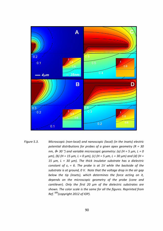
90
Figure 5.3. Microscopic (non-local) and nanoscopic (local) (in the insets) electric
potential distributions for probes of a given apex geometry (R = 30
nm, θ= 30 °) and variable microscopic geometry: (a) (H = 5 µm, L = 0
µm), (b) (H = 15 µm, L = 0 µm), (c) (H = 5 µm, L = 30 µm) and (d) (H =
15 µm, L = 30 µm). The thick insulator substrate has a dielectric
constant of εr = 6. The probe is at 1V while the backside of the
substrate is at ground, 0 V. Note that the voltage drop in the air gap
below the tip (insets), which determines the force acting on it,
depends on the microscopic geometry of the probe (cone and
cantilever). Only the first 20 µm of the dielectric substrates are
shown. The color scale is the same for all the figures. Reprinted from
Ref. 121
(copyright 2012 of IOP).
5. Quantifying the dielectric constant of thick insulators using EFM
91
The cantilever contribution, on the other hand, ∆C’dielec,cant(z, εr), shows a linear
behavior with the tip vertical displacement, Δz, (see Figures 5.2c and 5.2d,
insets), that is, '
, ( ; ) ( , , )dielec cant r dielec rC z a H L zε ε∆ ≈ ∆ . The slope adielec
increases when increasing L, decreasing H or increasing εr. To understand the
linear behavior of ∆C’dielec,cant(z, εr) with Δz, a similar reasoning as for metallic
substrate can be followed. Note that also in the case of dielectric substrates,
the direct contribution of the cantilever becomes comparable to the cone
contribution for small cone heights (H < L).
We can now explain the complex dependence of the total capacitance
gradient, ∆C’dielec (z, εr), on H and L given in Figures 5.2c and 5.2d. For probes
with a high cone (Figure 5.2d) (H > L) the total capacitance is dominated by the
cone contribution and hence it decreases when increasing the cantilever
dimensions (and also when increasing the cone height). Instead, for short cone
height probes (Figure 5.2c), when H < L, initially the capacitance gradient is
dominated by the cone and hence it decreases when increasing L, but at some
point it stops decreasing and starts increasing as a result of the direct
contribution from the cantilever.
In summary, it has been shown that the local electrostatic force between the
probe and a thick dielectric substrate depends on the microscopic geometry
and size of the cone and the cantilever mainly due to their indirect effects on
the local tip-substrate interaction. In addition, direct effects from the
cantilever can be relevant for short cone probes.
92
5.5 Quantification of the dielectric constant of
thick insulators
According to the results presented in section 5.4, the microscopic geometry of
the probe needs to be taken into account in any geometrical model used to
quantify the local dielectric constant of thick dielectric substrates using EFM. In
this section, we show that the simplified 2D axisymmetric model of Figure 5.1
can include them in an effective manner, thus optimizing the quantification
procedure demonstrated in Ref. 122
by adding a disc to the cone model that we
used.
We validated the method with the AM-EFM experiments performed on
different insulating substrates (PEN, PMMA, borosilicate glass, mica as
dielectric substrates and HOPG as metallic substrate) that we reported and
analyzed in Ref. 122
(experimental data kindly provided by Dra. L. Fumagalli).
This first set of experiments was obtained using commercial conductive
diamond coated probes (CDT-CONTR, Nanosensors). In addition, a second set
of measurements was performed on mica and HOPG using another type of
conductive diamond coated probes (CDT-FMR Nanosensors), which differ from
the previous one only in the cantilever size (450x50x2 μm3 vs 225x28x3 μm
3,
respectively), while they have similar cone heights (12.5 ± 2.5 μm, as obtained
from the datasheet), cone angles and apex radii. The spring constants of the
probes are different due to their different cantilever geometry (0.2 N/m vs 2.8
N/m, respectively).
As for the case of the numerical calculations, we obtained the capacitance
gradient variation ∆C’(z,εr) from the measured approach force curves F2ω(z,εr)
(see Ref.). The experiments were performed under dry environment (0% RH)
by flowing N2 through the AFM chamber to avoid water layers on the surfaces.
The dielectric constants of the substrates were obtained from the measured
capacitance gradient approach curves by using the 2D geometric model in
Figure 5.1 and following the two step procedure proposed in Ref. 122
, but
generalized to include a variable microscopic geometry. First, we calibrated
the apex geometry of the probe (R and θ) by a least square fitting of the
5. Quantifying the dielectric constant of thick insulators using EFM
93
metallic theoretical curve to the experimental curve taken on the metallic
substrate with H and L fixed to given initial values. Then, with the obtained
probe geometry, the dielectric constant was extracted by a least square fitting
of the dielectric theoretical curve to the experimental curve taken on the
insulator using the dielectric constant as the only fitting parameter. The same
procedure was then repeated for different values of the microscopic geometric
parameters H and L to evaluate how they affect the extracted dielectric
constant and the goodness of the fittings. The only constraint set to the values
of H and L was that the goodness of the fitting gave r2
> 0.9999.
Figure 5.4 shows the measured capacitance gradient curves obtained on (a)
mica, glass, PEN, PMMA and (inset) HOPG with the CDT-CONTR probe 122
, and
on (b) mica and (inset) HOPG with the CDT-FMR probe. Note that the noise in
Figure 5.4b is higher due to the higher spring constant of the CDT-FMR probes
as compared to the CDT-CONTR probes. Examples of the fittings obtained with
our procedure are given in Figure 5.4 (solid lines) for H = 12.5 µm and L = 3 µm,
showing very good fitting for both the insulating and metallic substrates.
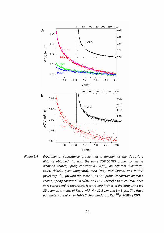
94
Figure 5.4 Experimental capacitance gradient as a function of the tip-surface
distance obtained (a) with the same CDT-CONTR probe (conductive
diamond coated, spring constant 0.2 N/m), on different substrates:
HOPG (black), glass (magenta), mica (red), PEN (green) and PMMA
(blue) (ref. 122
); (b) with the same CDT-FMR probe (conductive diamond
coated, spring constant 2.8 N/m), on HOPG (black) and mica (red). Solid
lines correspond to theoretical least square fittings of the data using the
2D geometric model of Fig. 1 with H = 12.5 µm and L = 3 µm. The fitted
parameters are given in Table 2. Reprinted from Ref. 121
(c 2009 of IOP).
5. Quantifying the dielectric constant of thick insulators using EFM
95
Similarly, good fittings can be obtained for other values of H and L. Figure 5.5
shows the extracted dielectric constant values, εr, together with the
geometrical parameters of the probe, R and θ obtained from the experimental
data in Figure 5.4a (CDT-CONTR probe) as a function of the cantilever disc
radius L and cone height H. In Figures 5.5a and 5.5b we observe that the
extracted tip radius and cone angle (R and θ) are practically not affected by the
microscopic probe geometry and size of the probe (H, L). This is because good
fittings are obtained only for H > L and for these values, the probe - metallic
substrate interaction is nearly independent of the microscopic geometry. On
the contrary, Figure 5.5c shows that for a given cone height, H, the extracted
dielectric constant increases when increasing L. Moreover, for a given
cantilever disc radius, the dielectric constant increases (decreases) when
increasing H for H > L (H< L). This behavior is clearly reminiscent of the
dependence of the local electrostatic interaction between the probe and the
thick insulating substrate described in section 5.4.
Remarkably, the dependence of the extracted dielectric constants on the
macroscopic parameters H and L for H > L can be described by the following
simple phenomenological relationship
[ ]0
( )( , ) 1 log ( ) 1
( )r r
L mH L H m H L
H m
µε ε α µ βµ
≈ + + >
, (4.2)
where, εr0, α and β are three parameters independent of H and L and given in
Table 5.1 for each substrate.
The results of Figure 5.5c demonstrate that the extracted dielectric constant
for a thick dielectric substrate significantly depends on the cantilever disc
radius, L, and on the cone height H. Therefore, care should be taken when
choosing these geometrical parameters to quantify the dielectric constant.
In Ref. 122
we showed that one can choose a simplified model that consists of
only the cone and no cantilever. There, we obtained good agreement with
nominal values, only slightly underestimating them, provided the cone height
was set to the higher value of the range given by the manufacturer, i.e. H = 15
µm (see Table 5.2).
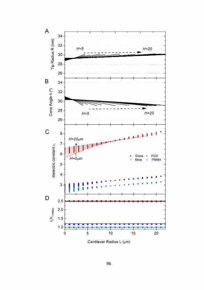
96
5. Quantifying the dielectric constant of thick insulators using EFM
97
Figure 5.5. Extracted apex radius (a), cone angle (b) and relative dielectric
constant (c) from the data plotted in Figure 5.4a by using the
theoretical model with variable L (0-30 µm) and different cone
heights H (5-20 µm). (continuous lines). The continuous lines in (c)
correspond to the predictions of Eq. (5.2) for the mica substrate. (d)
Extracted dielectric constants for glass, mica and PEN (symbols) as a
function of H and L, normalized by the values obtained for PMMA for
the same H and L. The ratios are almost independent of H and L and
roughly equal to the ratios of the nominal values (continuous lines).
The data of glass (black) are not visible, because they are identical to
the values obtained for mica (red). Only values of H and L giving a
fitting with r2
> 0.9999 have been considered. Reprinted from Ref. 121
(copyright 2012 of IOP).
Here, as an alternative approach, we demonstrate that one can obtain more
accurate values of the dielectric constant by including the contribution of the
cantilever and calibrating its effective length, that is the value of L, on a
reference substrate. For instance, if we set the cone height to its mean
manufacturer value (H = 12.5 µm) and use PMMA as reference substrate (ԑr =
2.6), we obtain L = 3 µm for the disc cantilever radius.
Using these geometrical values, for all the substrates analyzed in the present
paper we obtained dielectric constants in perfect agreement with nominal
values (see Table 5.2), while the cone model used in Ref. 122
gives slightly
smaller values. The additional calibration of L, then, provides a simple method
for accurate quantification of the dielectric constant of thick dielectric
substrates.
In summary, the dielectric constant of a given insulator substrate can be
obtained by fitting theoretical approach curves to measured ones, with the
dielectric constant as single fitting parameter, provided a probe geometry like
the one shown in Figure 5.1 is used with the cone height given by the
manufacturer, the apex radius and cone angle being determined from
approach curves on a metallic substrate and the effective cantilever radius
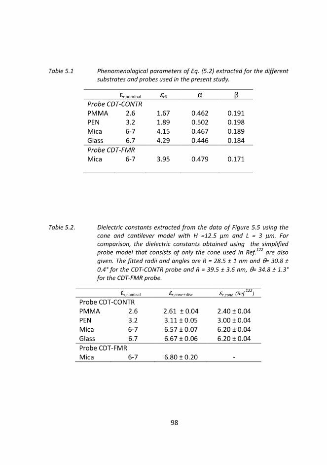
98
Table 5.1 Phenomenological parameters of Eq. (5.2) extracted for the different
substrates and probes used in the present study.
εr,nominal εr0 α β Probe CDT-CONTR
PMMA 2.6 1.67 0.462 0.191
PEN 3.2 1.89 0.502 0.198
Mica 6-7 4.15 0.467 0.189
Glass 6.7 4.29 0.446 0.184
Probe CDT-FMR
Mica 6-7 3.95 0.479 0.171
Table 5.2. Dielectric constants extracted from the data of Figure 5.5 using the
cone and cantilever model with H =12.5 µm and L = 3 µm. For
comparison, the dielectric constants obtained using the simplified
probe model that consists of only the cone used in Ref.122
are also
given. The fitted radii and angles are R = 28.5 ± 1 nm and θ= 30.8 ±
0.4° for the CDT-CONTR probe and R = 39.5 ± 3.6 nm, θ= 34.8 ± 1.3°
for the CDT-FMR probe.
εr,nominal εr,cone+disc εr,cone (Ref.122
)
Probe CDT-CONTR
PMMA 2.6 2.61 ± 0.04 2.40 ± 0.04
PEN 3.2 3.11 ± 0.05 3.00 ± 0.04
Mica 6-7 6.57 ± 0.07 6.20 ± 0.04
Glass 6.7 6.67 ± 0.06 6.20 ± 0.04
Probe CDT-FMR
Mica 6-7 6.80 ± 0.20 -
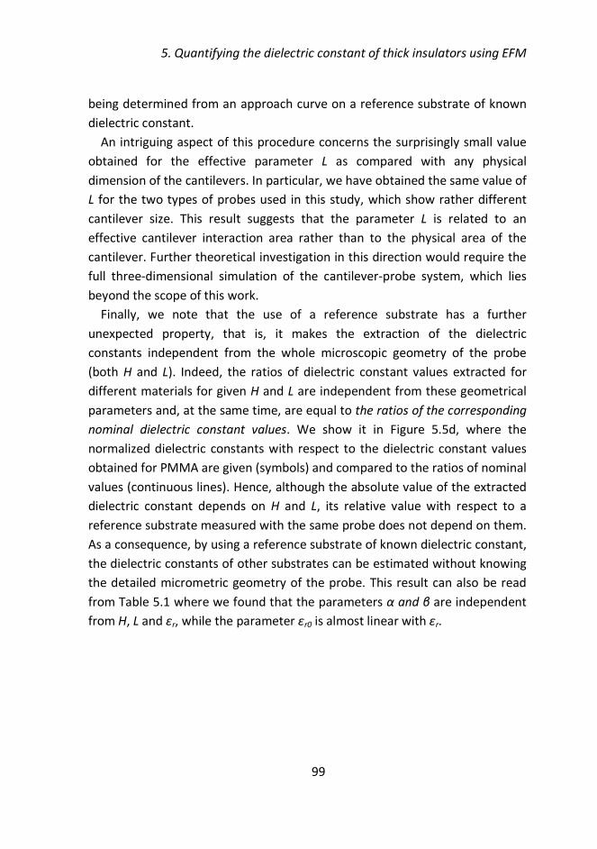
5. Quantifying the dielectric constant of thick insulators using EFM
99
being determined from an approach curve on a reference substrate of known
dielectric constant.
An intriguing aspect of this procedure concerns the surprisingly small value
obtained for the effective parameter L as compared with any physical
dimension of the cantilevers. In particular, we have obtained the same value of
L for the two types of probes used in this study, which show rather different
cantilever size. This result suggests that the parameter L is related to an
effective cantilever interaction area rather than to the physical area of the
cantilever. Further theoretical investigation in this direction would require the
full three-dimensional simulation of the cantilever-probe system, which lies
beyond the scope of this work.
Finally, we note that the use of a reference substrate has a further
unexpected property, that is, it makes the extraction of the dielectric
constants independent from the whole microscopic geometry of the probe
(both H and L). Indeed, the ratios of dielectric constant values extracted for
different materials for given H and L are independent from these geometrical
parameters and, at the same time, are equal to the ratios of the corresponding
nominal dielectric constant values. We show it in Figure 5.5d, where the
normalized dielectric constants with respect to the dielectric constant values
obtained for PMMA are given (symbols) and compared to the ratios of nominal
values (continuous lines). Hence, although the absolute value of the extracted
dielectric constant depends on H and L, its relative value with respect to a
reference substrate measured with the same probe does not depend on them.
As a consequence, by using a reference substrate of known dielectric constant,
the dielectric constants of other substrates can be estimated without knowing
the detailed micrometric geometry of the probe. This result can also be read
from Table 5.1 where we found that the parameters α and β are independent
from H, L and εr, while the parameter εr0 is almost linear with εr.
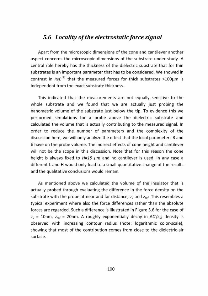
100
5.6 Locality of the electrostatic force signal
Apart from the microscopic dimensions of the cone and cantilever another
aspect concerns the microscopic dimensions of the substrate under study. A
central role hereby has the thickness of the dielectric substrate that for thin
substrates is an important parameter that has to be considered. We showed in
contrast in Ref.122
that the measured forces for thick substrates >100µm is
independent from the exact substrate thickness.
This indicated that the measurements are not equally sensitive to the
whole substrate and we found that we are actually just probing the
nanometric volume of the substrate just below the tip. To evidence this we
performed simulations for a probe above the dielectric substrate and
calculated the volume that is actually contributing to the measured signal. In
order to reduce the number of parameters and the complexity of the
discussion here, we will only analyze the effect that the local parameters R and
θ have on the probe volume. The indirect effects of cone height and cantilever
will not be the scope in this discussion. Note that for this reason the cone
height is always fixed to H=15 µm and no cantilever is used. In any case a
different L and H would only lead to a small quantitative change of the results
and the qualitative conclusions would remain.
As mentioned above we calculated the volume of the insulator that is
actually probed through evaluating the difference in the force density on the
substrate with the probe at near and far distance, z0 and zref. This resembles a
typical experiment where also the force differences rather than the absolute
forces are regarded. Such a difference is illustrated in Figure 5.6 for the case of
z0 = 10nm, zref = 20nm. A roughly exponentially decay in ΔC’(z0) density is
observed with increasing contour radius (note: logarithmic color-scale),
showing that most of the contribution comes from close to the dielectric-air
surface.
5. Quantifying the dielectric constant of thick insulators using EFM
101
∆∆∆∆C’(z) density(F/m4)
Rz0
θθθθ
zH
160
0.4⋅10-3
0.4
40 60 80 1001
10
100
R= 32nm, zref =150nm R= 32nm, zref = 20nm
R= 10nm, zref = 20nm R=100nm,zref = 20nm
cumulative ∆C'(zH) (%)
cone
hei
ght
z H (
nm)
0 100 200 300 400400
300
200
100
0
90%
70%
dept
h (
nm)
r (nm)
50%
∆∆∆∆C’(z) density(F/m4)
Rz0
θθθθ
zH
160
0.4⋅10-3
0.4
160
0.4⋅10-3
0.4
40 60 80 1001
10
100
R= 32nm, zref =150nm R= 32nm, zref = 20nm
R= 10nm, zref = 20nm R=100nm,zref = 20nm
cumulative ∆C'(zH) (%)
cone
hei
ght
z H (
nm)
0 100 200 300 400400
300
200
100
0
90%
70%
dept
h (
nm)
r (nm)
50%
Figure 5.6 Calculated locality of ∆C’(z) on a ~250mm thick insulator. The ∆C’(z0)
density in the substrate (z0 = 10 nm, zref = 20 nm, R = 32 nm, θ = 30º)
is given with the contours (dash lines) enclosing the 50%, 70% and
90% of the total variation. Inset: Plot of cumulative ∆C’(z0) along the
probe surface as a function of the cone height zH for different radii
and reference distances. Apex and cone regions of each curve are
plotted with thick and thin lines, respectively. Reprinted from Ref. 122
(copyright 2010 of AIP).
102
Integration within contours of equal value allows evaluation of the build up
of ΔC’(z0) while penetrating into the insulator. The integrated values of density
distribution, which gives the 50% of the signal confined in a hemispherical
region of r50% ~ 50 nm radius below the tip apex and the 70% within 100nm,
confirm the locality of the interaction. Note, however, that the 90% contour
penetrates rather deeply into the insulator down to ~ 400 nm. Interestingly
this volume does not shrink with the tip radius, e.g. r90% ~ 617 nm for R = 10
nm, whereas it is slightly smaller with larger tip radius, e.g. r90% ~ 360 nm for R
= 100 nm. This is because with smaller apex the signal is increasingly located
on the cone, thus spreading into a larger volume in the substrate.
This is evidenced in the inset of Figure 5.6, which plots the build-up of
ΔC’(z0) on the probe surface. The apex and cone region of each curve are
indicated as thick and thin lines, respectively and illustrate that for R = 32 nm,
z0 = 10nm and zref = 20 nm, the apex accounts for more than 90% of the total
variation, while it reaches 99% for R = 100 nm. Conversely, with smaller radii (R
= 10 nm) or larger reference distances (zref = 150 nm) the cone contribution
gains importance (22% and 28% respectively) and correspondingly the probed
volume in the insulator gets larger.
5. Quantifying the dielectric constant of thick insulators using EFM
103
5.7 Conclusion
In this chapter we demonstrated by means of finite-element numerical
calculations that the microscopic parts of an EFM probe (the cone and the
cantilever) affect the local electrostatic interaction between tip apex and a
thick insulator substrate, and hence the quantification of the dielectric
constant at the nanoscale.
We showed that these effects can be included into a simple 2D axisymmetric
probe model. By adding a disc with an effective radius that accounts for the
cantilever contribution, we optimized the quantification procedure that we
demonstrated in Ref. 122
based on a simple cone model.
Perfectly accurate dielectric constants can be obtained, provided that the
cone height is set similar to the real height of the cone and that the cantilever
disc radius is taken as a parameter that gives the effective interaction area of
the cantilever. This parameter is independent of the dielectric constant of the
substrate and hence it can be determined using a reference insulating
substrate of known dielectric constant.
Furthermore, the use of a reference substrate enables to obtain the
dielectric constants of other substrates even without knowing the detailed
microscopic geometry of the probe (cone height and disc radius).
These results offer a general framework under which accurate quantification
of the local dielectric constants of thick insulators can be achieved using EFM,
opening new possibilities for the dielectric characterization of insulating
materials at the nanoscale in general but especially for bio-samples that
cannot be measured on metallic substrates.
Also the fact that the actual volume that is probed in the insulating
substrate, was found to be located in a very confined region below the apex,
indicates that measurements of bio-membranes on thick insulating substrates
will be sensitive to the bio-membrane itself and quantitative extraction on
such materials will be possible. Experiments performed within our research
group confirms this assertion 123
(in preparation)

104
6. Dielectric constant of biomembranes in electrolyte solutions
105
6 Dielectric constant of biomembranes in
electrolyte solutions
6.1 Abstract
In the previous chapters we showed that dielectric constant quantification
of biomembranes on both metallic and insulating substrates can be performed
with nanoscale spatial resolution in air environment. However, the
physiological environment of biomembranes is an electrolyte solution. In the
present chapter we report quantitative imaging of the local dielectric
polarization properties of supported biomembranes in electrolyte solutions
with nanoscale spatial resolution. Local dielectric imaging has been achieved
by probing high frequency (>1 MHz) electric forces at the nanoscale, which, we
show, are dependent on the local dielectric properties of the materials. we
demonstrate the possibility to quantify these frequency and ionic
concentration dependent electric forces by means of finite element numerical
calculations including calibrated probe geometry, and deriving from it the
nanoscale dielectric constant of the materials in electrolyte solutions. The
developed method is demonstrated by imaging and quantifying the dielectric
properties of a 20 nm-thin SiO2 test microstructure and 5 nm-thin lipid bilayer
nanopatches. The technique shows high sensitivity to the dielectric properties
of the materials enabling distinguishing insulator materials with close dielectric
response. Present results open fascinating possibilities in fields like
Electrophysiology or Electrochemistry where quantitative measurements of
the nanoscale dielectric properties of materials under electrolyte solutions can
provide new insights not accessible until now.
106
This chapter reproduces almost literally the manuscript in preparation: " Nanoscale dielectric
polarizability of biomembranes and insulating thin films imaged and quantified in electrolyte
solutions", by G. Gramse, A. Dols, M. A. Edwards, L. Fumagalli and G. Gomila. In this manuscript I
was in charge of performing the experimental and the theoretical parts and of processing the
results. In this work I followed some experimental and theoretical suggestions by M. A. Edwards.
Moreover, the lipid bilayer samples were prepared by A. Dols-Pérez. The manuscript was written
by me in collaboration with my supervisor.
6.2 Introduction
We described in the Introduction of this thesis that one of the distinctive
aspects of Atomic Force Microscopy (AFM) is its capability to investigate
nanoscale phenomena in the liquid environment. This capability has made of
AFM an invaluable instrument for in situ imaging and surface characterization
of materials under liquids, with a strong impact in fields like Biology124, 125
or
Electrochemistry52, 126
, among others. The number of surface material
properties that can be determined with AFM based techniques under liquids
covers a wide range of possibilities, including surface stiffness127-129
,
electrochemical activity52, 130
, piezoelectric response95, 131, 132
or surface
charge/potential 60, 61, 63, 69, 73, 74, 77
.
But still at present some physical surface properties cannot be imaged
and quantified in the liquid environment with AFM based techniques. Among
them a major example refers to dielectric polarization, the property of
materials to orient permanent or induced electric dipoles in response to an
external electric field. Measuring dielectric polarization phenomena at the
nanoscale under electrolyte solutions is extremely challenging due to the
complex frequency dependent response of the electrified solid-electrolyte
interface and to the presence of large stray contributions preventing access to
local material properties. But yet dielectric information of material surfaces
under electrolyte solutions is fundamental to understand a broad variety of
electric phenomena in fields like Electrophysiology or Electrochemistry, where
dielectric properties of materials at the nanoscale in electrolyte solutions can
play an important role. This situation contrast with nanoscale dielectric
polarization studies of material surfaces in air, which can be thoroughly
6. Dielectric constant of biomembranes in electrolyte solutions
107
analyzed with a variety of techniques such as scanning capacitance
microscopy13
, scanning polarization force microscopy38
, scanning impedance
microscopy11, 14
, electrostatic force microscopy122, 133
or scanning microwave
microscopy98
.
In this chapter we propose and implement a high frequency (> 1 MHz)
Electrostatic Force Microscopy method for liquid imaging, and its
corresponding finite element numerical modeling, able to provide local
quantitative dielectric contrast of sample surfaces in electrolyte solutions with
nanoscale spatial resolution. High frequencies are used because we found that
at these frequencies the electric force acting on a conductive tip in close
proximity to a sample becomes local and sensitive to its local dielectric
polarization properties. The imaging and quantitative capabilities of the
technique are unambiguously demonstrated on a 20 nm thin silicon dioxide
microstructure and on 5 nm thin supported lipid bilayer nanopatches in
electrolyte solution.
6.3 Experimental Set up
The experimental set up used for the measurements is schematically
detailed in Figure 6.1. It consists of an AFM system compatible with both liquid
and electrical measurements. A voltage of frequency ωel in the MHz range,
whose amplitude is modulated with a frequency ωmod in the kHz range, is
applied between a conductive cantilever probe and the bottom of the sample.
The high frequency voltage, which is beyond the cantilever mechanical
resonance frequency, bends the cantilever in a static way due to the non-linear
dependence of the actuation force on the applied voltage. The low frequency
signal modulates this cantilever bending allowing an increased signal to noise
detection. Dielectric images are obtained by scanning the probe at constant
height with respect to the substrate at distances much larger than the Debye
screening length (which is typically 10 nm in 1mM electrolyte solutions).
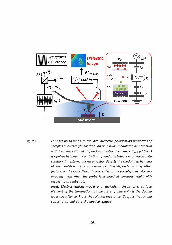
108
Figure 6.1 EFM set up to measure the local dielectric polarization properties of
samples in electrolyte solution. An amplitude modulated ac-potential
with frequency ωel (>MHz) and modulation frequency ωmod (<10kHz)
is applied between a conducting tip and a substrate in an electrolyte
solution. An external lockin amplifier detects the modulated bending
of the cantilever. The cantilever bending depends, among other
factors, on the local dielectric properties of the sample, thus allowing
imaging them when the probe is scanned at constant height with
respect to the substrate.
Inset: Electrochemical model and equivalent circuit of a surface
element of the tip-solution-sample system, where Cdl is the double
layer capacitance, Rsol is the solution resistance, Csample is the sample
capacitance and Vac is the applied voltage.
6. Dielectric constant of biomembranes in electrolyte solutions
109
6.4 Theory of Electrostatic Force in Liquid
This experimental set up is able to produce local dielectric images of material
surfaces in electrolyte solutions for applied frequencies above a critical
frequency in the >MHz range due to the frequency dependent response of the
force acting on the probe. Indeed, in an electrolyte solution the electric force
acting on the conducting probe in response to an ac applied voltage Vac(t) is
given by 134
2( )1( , ) ( , )
2s o l
e le c s o l
C zF z t V z t
z
∂=∂
(6.1)
where Vsol is the voltage drop in the solution and Csol is the capacitance of the
solution gap between probe and sample. From the analysis of the equivalent
circuit for the probe-solution-sample system sketched in the inset in Figure 6.1
one finds that the voltage drop in the solution is dependent on the dielectric
properties of the sample (see details in appendix). In particular, it can be
shown that the voltage drop in the solution, and hence the electric force, are
detected only for frequencies higher than a critical frequency, fact given by
( )1 2act sol eq solf R C Cπ− = + where Rsol is the solution resistance and Ceq is
given by ( )2eq dl sample dl sampleC C C C C= ⋅ + with Csample and Cdl being the sample
and double layer capacitances, respectively.
An estimation of fact can be obtained by assuming a simple parallel plate model
for the cantilever and for the tip end and neglecting double layer contributions
(see appendix), giving
1 1
, ,
0 , , ,
( )1 3 ( ) 1
2 ( )r sample r sample
actr water r water r water
z z nmcf MHz c mM
h h nm
ε επ ε ε ε ε
− − ⋅Λ= + ≈ ⋅ + ⋅ ⋅
(6.2)
110
where c is the solution ionic concentration, Λ the molar conductivity, h the
thickness of the sample, εr,water=78 is the relative dielectric constant of water,
εr,sample the sample relative dielectric constant and z the distance between the
sample and the tip (or cantilever). Assuming typical experimental parameters,
i.e. Λ=13.3 S m-1
mol-1
, c=1 mM, h=10 nm and εr=4, and taking z=z0=10 nm for
the tip-sample distance and z=H+z0 for the cantilever-sample distance, where
H =10 µm is the cone height, we obtain fact,cant=60 kHz and fact,tip=3 MHz, for the
cantilever and tip, respectively. Therefore cantilever electric actuation can be
achieved in electrolyte solutions for frequencies f> fact,cant~kHz but local
dielectric contrast can only be measured when f> fact,apex~MHz.
6.5 Materials and Methods
In order to validate this theoretical prediction we have considered a test
structure consisting of a 20 nm thin silicon dioxide stripe 2.5 µm wide on a
highly doped silicon substrate. Experiments have been performed with a
commercial AFM (Nanotec Electronica S.L.) equipped with a custom made
liquid cell compatible with electrical measurements made from Teflon and
using apiezon-wax for sealing. Solid platinum tips from Rocky Mountain
Nanotechnology with a spring constant of k~0.3N/m and resonance frequency
in solution of ~6 kHz were used. All solutions were prepared from MilliQ and
KClO4. We used the Agilent 33250A as external waveform generator and an
external Anfatec eLockIn 204/2 to modulate the signal. For the quantitative
interpretation of the experiments finite element numerical simulations have
been performed with Comsol MultiPhysics 4.0, in which we modeled the AFM-
tip as a truncated cone of height H with an aperture angle, θ, plus a spherical
apex of radius R located at a distance, z, above the dielectric sample of height,
h, diameter, D, and dielectric constant εr. To account for the very thin layer of
native oxide on the silicon substrate a distributed capacitance was added on
the conducting part of the substrate, Cnative (see appendix for further details on
the numerical calculations). To make forces measured at different applied
6. Dielectric constant of biomembranes in electrolyte solutions
111
voltages comparable we represent in all experiments a normalized value with
units of capacitance gradient, 2
,0'( ) 2 elec acC z F V= .
6.6 Results
In Figure 6.2a a topographic image of the Si02 microstructure obtained
in conventional intermittent contact mode is shown together with the
dielectric images obtained in aqueous electrolyte solutions for two ionic
concentrations 1 mM (Figure 6.2b) and 10 mM (Figure 6.2c). The dielectric
images were measured with the tip scanning at constant height (z=100nm)
over the baseline of the substrate and changing the frequency of the applied
voltage every 10 lines from 20MHz (top) to 100kHz (bottom).
As it can be seen the dielectric images nicely reproduce the presence of the
20nm thin silicon dioxide stripes showing the capability to perform local
dielectric images in electrolyte solutions. We note from the images that there
is only local contrast for applied frequencies above a given characteristic value,
which is here f>100 kHz for c=1 mM and f>1MHz for c=10 mM. This is in
agreement with the simple dependence of the critical actuation frequency on
ion concentration predicted from Equation (6.2), fact~c. As shown in Figure
6.2d, for rising frequencies the contrast increases monotonically over two
orders of magnitude until it plateaus at about 10 MHz for c=1 mM and about
100 MHz (estimated) for c=10 mM. Due to the specific cone geometry this
crossover is much smoother than it would be predicted from the simple
parallel plate model. We verified this with numerical calculations including a
realistic cone geometry for the probe (see appendix for further information).
Notice that due to the high dielectric constant of water (εr,water=78) the
measured capacitance gradients are almost two orders of magnitude higher
than in air (εr,air=1) thus allowing to reach excellent signal to noise ratios by
applying the small voltages required to avoid electrochemical surface reactions
(here Vac,p=0.5 V).
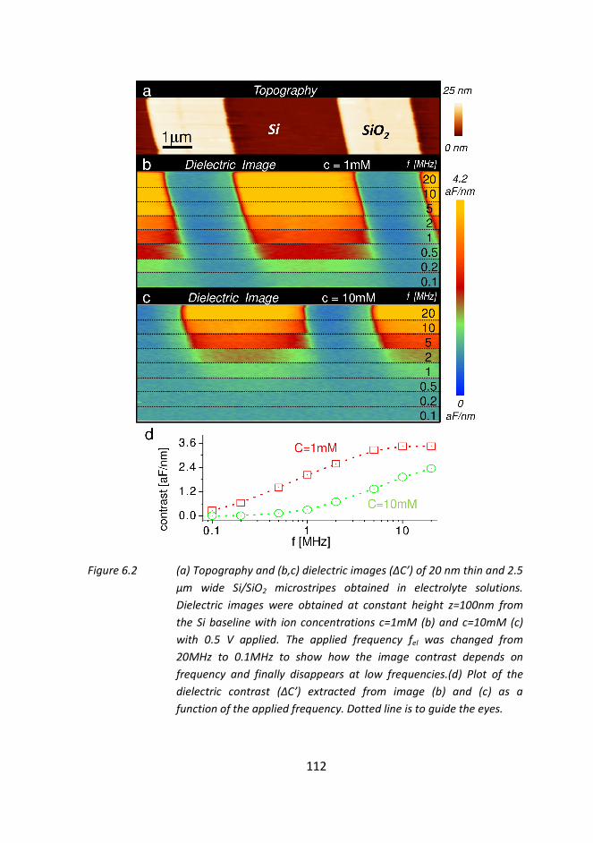
112
Figure 6.2 (a) Topography and (b,c) dielectric images (ΔC’) of 20 nm thin and 2.5
µm wide Si/SiO2 microstripes obtained in electrolyte solutions.
Dielectric images were obtained at constant height z=100nm from
the Si baseline with ion concentrations c=1mM (b) and c=10mM (c)
with 0.5 V applied. The applied frequency fel was changed from
20MHz to 0.1MHz to show how the image contrast depends on
frequency and finally disappears at low frequencies.(d) Plot of the
dielectric contrast (ΔC’) extracted from image (b) and (c) as a
function of the applied frequency. Dotted line is to guide the eyes.
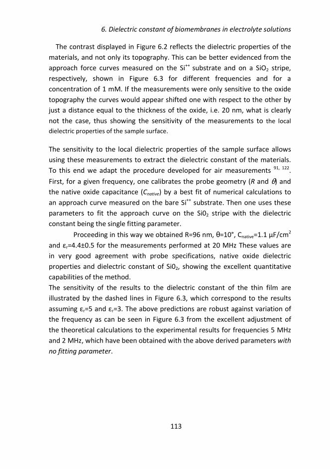
6. Dielectric constant of biomembranes in electrolyte solutions
113
The contrast displayed in Figure 6.2 reflects the dielectric properties of the
materials, and not only its topography. This can be better evidenced from the
approach force curves measured on the Si++
substrate and on a SiO2 stripe,
respectively, shown in Figure 6.3 for different frequencies and for a
concentration of 1 mM. If the measurements were only sensitive to the oxide
topography the curves would appear shifted one with respect to the other by
just a distance equal to the thickness of the oxide, i.e. 20 nm, what is clearly
not the case, thus showing the sensitivity of the measurements to the local
dielectric properties of the sample surface.
The sensitivity to the local dielectric properties of the sample surface allows
using these measurements to extract the dielectric constant of the materials.
To this end we adapt the procedure developed for air measurements 91, 122
.
First, for a given frequency, one calibrates the probe geometry (R and θ) and
the native oxide capacitance (Cnative) by a best fit of numerical calculations to
an approach curve measured on the bare Si++
substrate. Then one uses these
parameters to fit the approach curve on the Si02 stripe with the dielectric
constant being the single fitting parameter.
Proceeding in this way we obtained R=96 nm, θ=10°, Cnative=1.1 µF/cm2
and εr=4.4±0.5 for the measurements performed at 20 MHz These values are
in very good agreement with probe specifications, native oxide dielectric
properties and dielectric constant of Si02, showing the excellent quantitative
capabilities of the method.
The sensitivity of the results to the dielectric constant of the thin film are
illustrated by the dashed lines in Figure 6.3, which correspond to the results
assuming εr=5 and εr=3. The above predictions are robust against variation of
the frequency as can be seen in Figure 6.3 from the excellent adjustment of
the theoretical calculations to the experimental results for frequencies 5 MHz
and 2 MHz, which have been obtained with the above derived parameters with
no fitting parameter.
114
Figure 6.3 (Symbols) Approach curves onto the Si++
and the SiO2 parts of the
microstructure measured at various frequencies in electrolyte solutions
(c=1mM and Vac=0.5 V). Solid lines represent numerical results obtained
considering a probe with tip radius R=96nm, cone angle θ=10°, a native
oxide capacitance Cnative=1.1µF/cm2 and a dielectric constant εr,oxide=4.
Dashed lines represent εr,oxide=3 and 5. Additional model parameters
used in the numerical calculations are: cone height H=10 µm, Si02
thickness h=20 nm and Si02 diameter D=3 µm. Insets show the respective
simulated potential distributions for two frequencies (20 MHz and 100
KHz).
6. Dielectric constant of biomembranes in electrolyte solutions
115
Only at lower frequencies and for very close distances to the surface the
theoretical predictions deviate from the measurements since the model does
not include the true 3D sample geometry and the effect of double layer
capacitances, which become relevant in the corresponding situations. The
above results show unambiguously that the local dielectric constant of
materials can be obtained in electrolyte solutions with the proposed
technique.
Further insight on why the measurements are sensitive to the local dielectric
properties of the sample can be gained by comparing the calculated potential
distributions shown in the insets of Figure 6.3 for a high frequency (20 MHz)
and a low frequency (100 kHz). As it can be seen, only at high frequencies a
potential gradient develops below the tip enabling field lines of different
intensity to pass through the oxide layer leading to an electrostatic force on
the apex sensitive to the local oxide dielectric properties.
As an example of application of the developed methodology, we consider
the determination of the local dielectric constant of biomembranes in
electrolytic solutions. As we have mentioned earlier, the dielectric constant of
biomembranes is a parameter especially important in cell electrophysiology as
it ultimately determines the ion membrane permeability, the membrane
potential formation or the action potential propagation velocity, among
others93, 135-137
. Knowing the dielectric properties of biomembranes with
nanoscale spatial resolution is very important due to the nanoscale
hetereogeneous composition of plasma membranes (e.g. lipid rafts). However,
no technique is able to provide this quantity with the required nanoscale
spatial resolution and in electrolyte solution. As representative model of a
biomembrane we consider here dipalmitoylphosphatidylcholine (DPPC) single
bilayers. Phosphatidylcholines are the main components of eukaryotic cell
membranes138
, and DPPC is one of the most widely used phosphatidylcholine models.
The DPPC bilayer patches have been formed on the Si/Si02 sample studied
above by means of the liposome fusion technique.
Figure 6.4 shows the topography (a) and phase (b) images of a single DPPC
bilayer (5 nm thin) adsorbed onto the Si/SiO2-sample in an aqueous solution
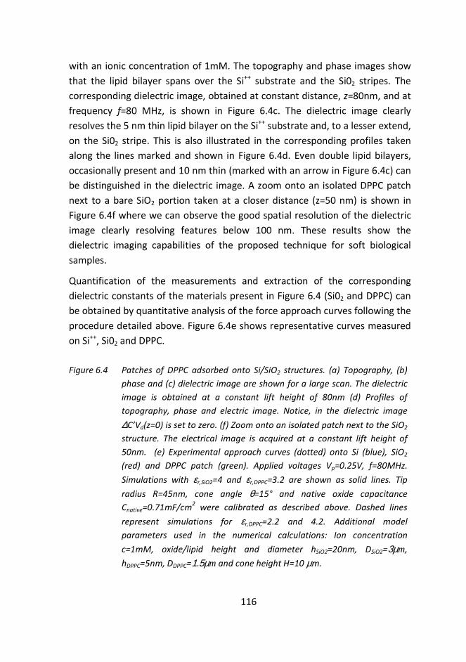
116
with an ionic concentration of 1mM. The topography and phase images show
that the lipid bilayer spans over the Si++
substrate and the Si02 stripes. The
corresponding dielectric image, obtained at constant distance, z=80nm, and at
frequency f=80 MHz, is shown in Figure 6.4c. The dielectric image clearly
resolves the 5 nm thin lipid bilayer on the Si++
substrate and, to a lesser extend,
on the Si02 stripe. This is also illustrated in the corresponding profiles taken
along the lines marked and shown in Figure 6.4d. Even double lipid bilayers,
occasionally present and 10 nm thin (marked with an arrow in Figure 6.4c) can
be distinguished in the dielectric image. A zoom onto an isolated DPPC patch
next to a bare SiO2 portion taken at a closer distance (z=50 nm) is shown in
Figure 6.4f where we can observe the good spatial resolution of the dielectric
image clearly resolving features below 100 nm. These results show the
dielectric imaging capabilities of the proposed technique for soft biological
samples.
Quantification of the measurements and extraction of the corresponding
dielectric constants of the materials present in Figure 6.4 (Si02 and DPPC) can
be obtained by quantitative analysis of the force approach curves following the
procedure detailed above. Figure 6.4e shows representative curves measured
on Si++
, Si02 and DPPC.
Figure 6.4 Patches of DPPC adsorbed onto Si/SiO2 structures. (a) Topography, (b)
phase and (c) dielectric image are shown for a large scan. The dielectric
image is obtained at a constant lift height of 80nm (d) Profiles of
topography, phase and electric image. Notice, in the dielectric image
∆C’Vd(z=0) is set to zero. (f) Zoom onto an isolated patch next to the SiO2
structure. The electrical image is acquired at a constant lift height of
50nm. (e) Experimental approach curves (dotted) onto Si (blue), SiO2
(red) and DPPC patch (green). Applied voltages Vp=0.25V, f=80MHz.
Simulations with εr,SiO2=4 and εr,DPPC=3.2 are shown as solid lines. Tip
radius R=45nm, cone angle θ=15° and native oxide capacitance
Cnative=0.71mF/cm2 were calibrated as described above. Dashed lines
represent simulations for εr,DPPC=2.2 and 4.2. Additional model
parameters used in the numerical calculations: Ion concentration
c=1mM, oxide/lipid height and diameter hSiO2=20nm, DSiO2=3µm,
hDPPC=5nm, DDPPC=1.5µm and cone height H=10 µm.
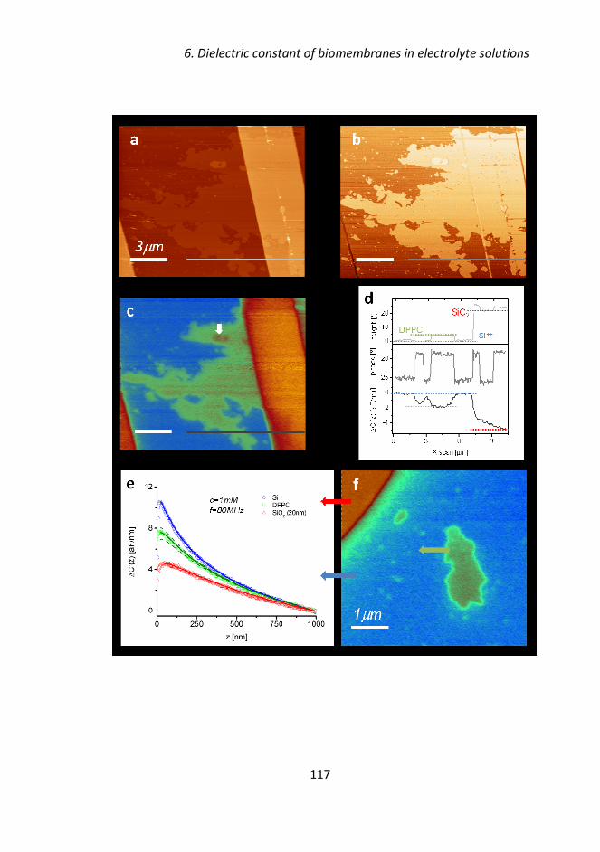
6. Dielectric constant of biomembranes in electrolyte solutions
117
118
6.7 Discussion
Quantification of the measurements gives εr,Si02=4±0.2 for the Si02, confirming
the above findings, and εr,DPPC=3.2±0.1 (error bounds from the fitting routine)
for the DPPC lipid bilayer. This value is slightly larger than the usual theoretical
value quoted for the hydrophobic part of lipid bilayers 139
(εr=2-2.5), or the
nanoscale value measured by us in dry air conditions for the so called purple
membrane 19, 91
. However, it is remarkably close to εr~3140, 141
predicted by
recent simulations including the contributions from the water/lipid interface
and polar heads. Moreover, putting together the bilayer thickness and the
obtained dielectric constant the capacitance per unit area of the DPPC bilayer
turns out to be cm=ε0 εr,DPPC/h=0.57 µF/cm2. This value is in excellent
agreement with experimental values reported in literature and obtained from
macroscopic impedance based measurements on supported lipid DPPC layers
on gold electrodes (cm =0.52-0.57 µF/cm2)
142. The proposed approach then has
demonstrated the capability to quantify the dielectric constant of a
biomembrane with the great advantage over macroscopic techniques to
provide also information on the thickness of the sample and a spatial
resolution below 100 nm.
In the present implementation of the technique we showed a spatial
resolution below 100 nm and a remarkable sensitivity to the dielectric
constant of the materials, which can discriminate between materials of
relatively close dielectric response such as silicon dioxide (εr~4) and lipids
(εr~3). These results, however, do not represent the absolute limits of the
technique. At present the technique is essentially limited by the need to be
operated at distances larger than several times the Debye screening length. By
using novel instrumental advances and appropriate theoretical models, it
should be possible to remove this limitation and increase both the spatial
resolution and the dielectric sensitivity of the technique.
6. Dielectric constant of biomembranes in electrolyte solutions
119
6.8 Conclusion
In summary, we have demonstrated for the first time imaging and
successful quantification of dielectric polarization properties on material
surfaces in electrolyte solutions with nanometric spatial resolution. The
proposed technique is applicable to both inorganic samples and biosamples,
thus opening a number of fascinating possibilities in fields like
Electrophysiology or Electrochemistry where nanoscale information on the
dielectric properties of materials under electrolyte solutions was not
accessible until now.
120
6.9 Appendix
6.9.1 Dependency of electric force on voltage drop in
solution Vsol and sample dielectric constant εεεεr
In an electrolyte solution the electric force acting on the conducting probe in
response to an applied ac voltage ( ),0( ) sinac acV t V tω= ⋅ is given by 134
2( )1( , ) ( )
2so l
e lec so l
C zF z t V z
z
∂=∂
(6.3)
The relationship between the voltage drop in the solution and the applied
voltage can be obtained by solving the circuit depicted in Figure 6.5. The
following derivations in this paragraph are based on a parallel plate model.
After some algebra one finds:
( ),0 22
/( )
1 1/ 1/
eqsol ac
eq sol
f fV V
f f fω =
+ + (6.4)
where we have introduced two characteristic frequencies given by
1 2eq eq solf C Rπ− =
and 1 2sol sol solf C Rπ− = and the equivalent capacitance
corresponding to the series combination of the sample capacitance and double
layer capacitance ( )2eq dl sample dl sampleC C C C C= ⋅ + . Notice, that since the
double layer capacitance is usually much bigger than the sample capacitance it
can be neglected except for the case when measuring a metallic substrate with
a metallic tip.
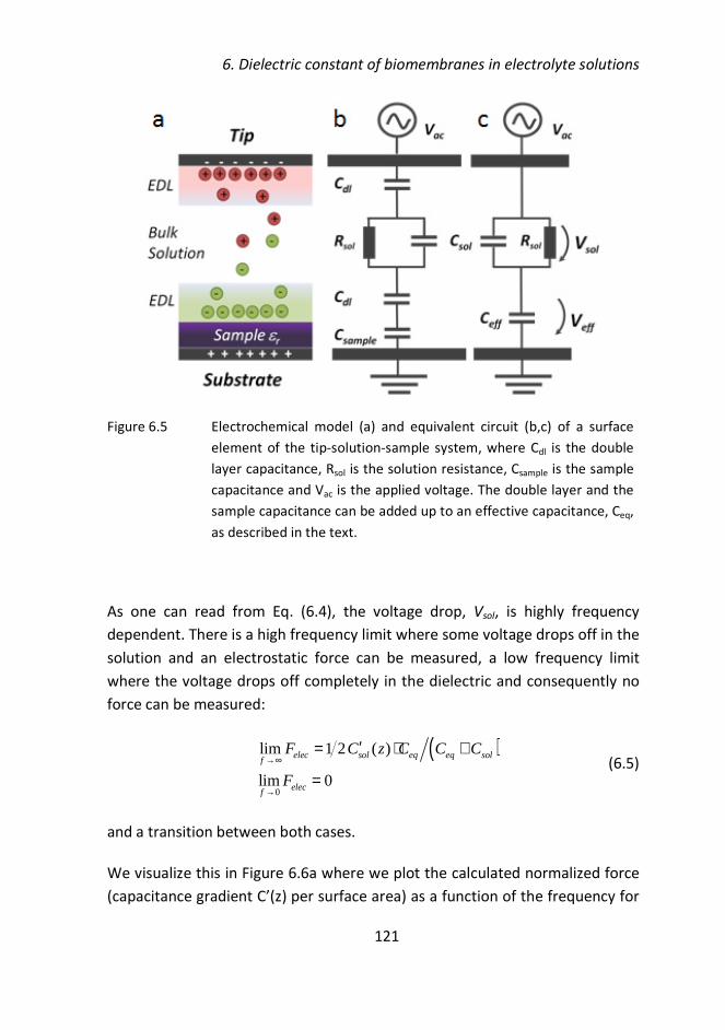
6. Dielectric constant of biomembranes in electrolyte solutions
121
Figure 6.5 Electrochemical model (a) and equivalent circuit (b,c) of a surface
element of the tip-solution-sample system, where Cdl is the double
layer capacitance, Rsol is the solution resistance, Csample is the sample
capacitance and Vac is the applied voltage. The double layer and the
sample capacitance can be added up to an effective capacitance, Ceq,
as described in the text.
As one can read from Eq. (6.4), the voltage drop, Vsol, is highly frequency
dependent. There is a high frequency limit where some voltage drops off in the
solution and an electrostatic force can be measured, a low frequency limit
where the voltage drops off completely in the dielectric and consequently no
force can be measured:
( )0
lim 1 2 ( )
lim 0
elec sol eq eq solf
elecf
F C z C C C
F
→∞
→
′= ⋅ +
= (6.5)
and a transition between both cases.
We visualize this in Figure 6.6a where we plot the calculated normalized force
(capacitance gradient C’(z) per surface area) as a function of the frequency for
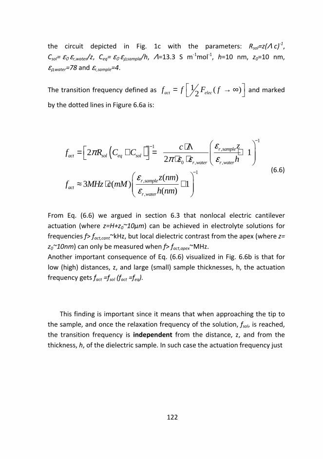
122
the circuit depicted in Fig. 1c with the parameters: Rsol=z(Λ c)-1
,
Csol= ε0 εr,water/z, Ceq= ε0 ερ,sample/h, Λ=13.3 S m-1
mol-1
, h=10 nm, z0=10 nm,
ερ,water=78 and εr,sample=4.
The transition frequency defined as 1 ( )2act elecf f F f = → ∞ and marked
by the dotted lines in Figure 6.6a is:
( )1
1 ,
0 , ,
1
,
,
2 12
( )3 ( ) 1
( )
r sampleact sol eq sol
r water r water
r sampleact
r water
zcf R C C
h
z nmf MHz c mM
h nm
επ
π ε ε ε
εε
−−
−
⋅Λ = + = + ⋅ ⋅
≈ ⋅ +
(6.6)
From Eq. (6.6) we argued in section 6.3 that nonlocal electric cantilever
actuation (where z=H+z0~10μm) can be achieved in electrolyte solutions for
frequencies f> fact,cant~kHz, but local dielectric contrast from the apex (where z=
z0~10nm) can only be measured when f> fact,apex~MHz.
Another important consequence of Eq. (6.6) visualized in Fig. 6.6b is that for
low (high) distances, z, and large (small) sample thicknesses, h, the actuation
frequency gets fact =fsol (fact =feq).
This finding is important since it means that when approaching the tip to
the sample, and once the relaxation frequency of the solution, fsol, is reached,
the transition frequency is independent from the distance, z, and from the
thickness, h, of the dielectric sample. In such case the actuation frequency just
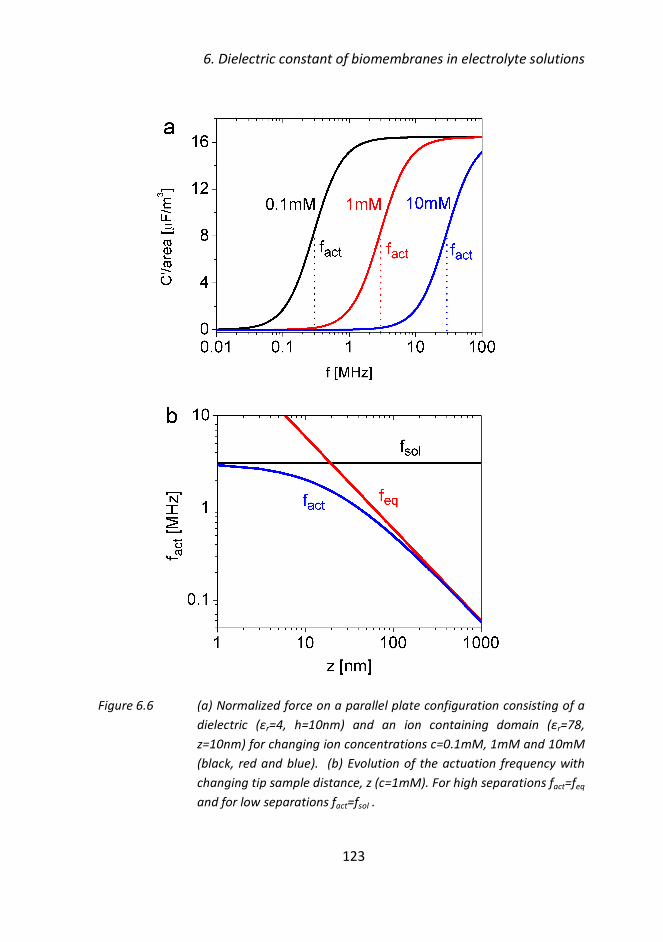
6. Dielectric constant of biomembranes in electrolyte solutions
123
Figure 6.6 (a) Normalized force on a parallel plate configuration consisting of a
dielectric (εr=4, h=10nm) and an ion containing domain (εr=78,
z=10nm) for changing ion concentrations c=0.1mM, 1mM and 10mM
(black, red and blue). (b) Evolution of the actuation frequency with
changing tip sample distance, z (c=1mM). For high separations fact=feq
and for low separations fact=fsol .
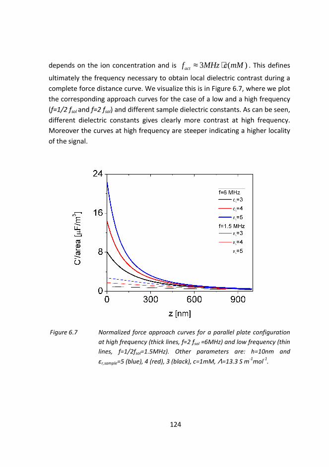
124
depends on the ion concentration and is 3 ( )actf MHz c mM≈ ⋅ . This defines
ultimately the frequency necessary to obtain local dielectric contrast during a
complete force distance curve. We visualize this is in Figure 6.7, where we plot
the corresponding approach curves for the case of a low and a high frequency
(f=1/2 fsol and f=2 fsol) and different sample dielectric constants. As can be seen,
different dielectric constants gives clearly more contrast at high frequency.
Moreover the curves at high frequency are steeper indicating a higher locality
of the signal.
Figure 6.7 Normalized force approach curves for a parallel plate configuration
at high frequency (thick lines, f=2 fsol =6MHz) and low frequency (thin
lines, f=1/2fsol=1.5MHz). Other parameters are: h=10nm and
εr,sample=5 (blue), 4 (red), 3 (black), c=1mM, Λ=13.3 S m-1
mol-1
.
6. Dielectric constant of biomembranes in electrolyte solutions
125
6.9.2 Data Interpretation using Finite Element simulations
Measured forces obtained with the described heterodyne detection
method were normalized to give mod
2 20 , 0'( ) 2 4elec elec fC z F V F V= = , where V0
is the amplitude of the applied ac-potential with the frequency f and mod,elec fF is
the measured electrostatic force modulated at a frequency fmod.
For the quantitative interpretation of the experiments we compared our
results to forces calculated with a finite element model of the AFM tip above
the dielectric sample and substrate. To obtain the electrostatic force acting on
the specific tip geometry the equation ( )( )0 0ri Vσ ωε ε∇ + ∇ = was solved
using the electrostatic AC/DC module of Comsol Multiphysics 4.0, and from its
solution, the harmonic force on the AFM-tip was calculated by using the built-
in Maxwell stress tensor. All simulations were carried out in the 2D
axisymmetric mode (electric quasistatics, meridional electric currents).
The geometry was defined like shown in Figure 6.8 with the tip
parameters: tip radius, R, cone angle, θ, and cone height H. The sample is
defined by the parameters: sample height, h, sample radius, l, and sample
dielectric constant εr,mem. Notice, the sample is a cylinder since we are working
in axisymmetric 2D mode. To account for the native oxide on the highly doped
silicone sample we added a distributed capacitance on top of the conducting
substrate that is set to ground. The solution is defined by its dielectric constant
εr,sol and its solution conductivity σsol =c Λsol, depending on the electrolyte
concentration, c, and the molar conductivity Λsol.
The domain containing the solution is enclosed by the outer boundary
conditions electric insulation or 0n J⋅ =��
. Notice, in order to cancel out any
effect from the finite size of the simulated volume we added an additional
outer simulation box where we use the function “infinite elements” to move
the outer boundaries to infinity. The defined geometry was meshed refining
especially the tip and sample surface and solved using the parametric solver
PARDISO with the frequency as parameter. The Maxwell-Stress-Tensor was
integrated over the whole tip surface to obtain the tip force.
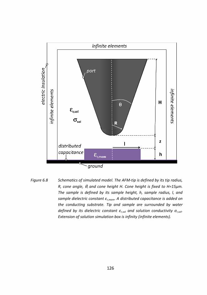
126
Figure 6.8 Schematics of simulated model. The AFM-tip is defined by its tip radius,
R, cone angle, θ, and cone height H. Cone height is fixed to H=15µm.
The sample is defined by its sample height, h, sample radius, l, and
sample dielectric constant εr,mem. A distributed capacitance is added on
the conducting substrate. Tip and sample are surrounded by water
defined by its dielectric constant εr,sol and solution conductivity σr,sol.
Extension of solution simulation box is infinity (infinite elements).
6. Dielectric constant of biomembranes in electrolyte solutions
127
To facilitate the data analysis simulations were carried out for an extensive
set of parameters (R = 25-125 nm; θ = 10−30 °; h = 5, 20nm; l = 750, 1500 µm;
c = 0.1, 1, 10 mM; f = 20 kHz – 80 MHz; z = 10- 1000 nm; Cthin = 0.035-0.25 F/m2,
εr,mem = 2-10) and the data was interpolated using Mathematica 7 to obtain
finally a fitting function for the experimental data analysis. In this way we are
able to investigate the effect of every simulation parameter almost like with a
normal analytical function and we can extract the sample-dielectric constant
fitting best to the measured data.
6.9.3 Calculating Forces: Parallel Plate Model versus Cone
Model Simulations
Although, many valuable insights can be gained from investigating the
electrostatic force in a parallel plate configuration, there are substantial
quantitative differences between the force in such a configuration and the
more realistic tip cone-substrate model. We show this in Fig. 5 where we plot
(a) the frequency dependency of the force at z=15nm and (b) the distance
dependency of the force at a fixed frequency f=20MHz for the parallel plate
model (thick line) and the cone model (dashed line). The forces are calculated
for a 5nm thin and laterally infinite dielectric of εr=4. As one observes in Figure
6.9a the frequency transition is much smoother for the cone model and
(nonlocal) forces are still present at frequencies below 100 kHz. In general it
becomes difficult to define a unique transition frequency since apex and cone
contribute at different frequencies. Also the approach curves at fixed distance
are much smoother for the cone model and rise for z>100nm almost
logarithmically with decreasing distance, whereas in the parallel plate model
the forces rise much steeper close to the surface.
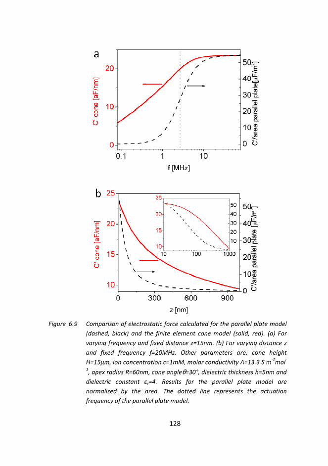
128
Figure 6.9 Comparison of electrostatic force calculated for the parallel plate model
(dashed, black) and the finite element cone model (solid, red). (a) For
varying frequency and fixed distance z=15nm. (b) For varying distance z
and fixed frequency f=20MHz. Other parameters are: cone height
H=15µm, ion concentration c=1mM, molar conductivity Λ=13.3 S m-1
mol-
1, apex radius R=60nm, cone angleθ=30°, dielectric thickness h=5nm and
dielectric constant εr=4. Results for the parallel plate model are
normalized by the area. The dotted line represents the actuation
frequency of the parallel plate model.
6. Dielectric constant of biomembranes in electrolyte solutions
129

130
7. Conclusion and Summary
131
7 Conclusion and Summary
7.1 Conclusions
The initial objective of my thesis consisted in the development of a current
sensing-AFM based technique to measure the dielectric constant of biological
samples in their natural ion containing liquid environment. However, with the
time we noticed, also from theoretical calculations that this is going to be a
very tough aim. The primary experimental difficulty, as also noticed by other
researchers, is to develop a probe that can be used to measure topography,
but at the same time shields well stray capacitances and can be used for local,
electrical current measurements. To approach the problem from a different
direction, I also started to test EFM to see whether one can perform
quantitative dielectric measurements of biosamples on metallic substrates
with it – at this time still in air. And as I showed in chapter 4 even in a DC-
detection mode this yielded very good quantitative results of the dielectric
constant on purple membrane patches.
I continued with EFM experiments also in the AC-detection mode what
encouraged me and also the rest of the group to further explore the
capabilities of EFM. In continuation I worked on another more theoretical
aspect that was dealing with the interpretation of measurements on insulating
substrates like mica. This came just very recently to an end and the scientific
community and our group has now a systematic methodology to analyze also
dielectric measurements on insulating substrates. This extends the
applicability of dielectric measurements to a considerably bigger number of
biological samples that require insulating substrates like glass or mica.
132
However, through all this time in parallel I was trying to make EFM also
work in liquid and to elucidate experimentally and theoretically the origin of
electrostatic forces in liquid solution. At some point I probably asked myself
the right question and I did the right experiments to understand that the
frequency-dependency of the electrostatic force is the key. The final result of
all this work is the successful implementation of an EFM-based technique to
measure the dielectric constant of biosamples in liquid solution as I showed in
chapter 6 on the example of lipid bilayers. This technique allows now the
investigation of polarization properties of systems that only remain stable in
ion containing liquid solutions. Therefore it may open completely new areas of
research in the field of Biology.
7. Conclusion and Summary
133
7.2 Perspectives
The thesis presented here is no closed work and as mentioned in chapter 5
the group is working on the application of the accumulated knowledge to new
experiments. Now, that we have a better understanding on the origin of the
electrostatic force in thick insulating substrates, also measurements of
biomembranes and other samples on these substrates can be interpreted and
the dielectric constant can be extracted.
The new developed EFM-technique for measurements in liquid
environment is ready to be used for the study on relevant biological
membrane-systems. Currently, we are working on the measurement of multi-
component phospholipid systems to investigate whether there is a dielectric
contrast between both components and if it is big enough to be resolved. This
would enable the use of this technique to resolve membrane domains in a
label free way which cannot be distinguished solely by their topography.
Then, probably also other membrane systems can be investigated and by
increasing the measurement-frequency it will be also possible to increase the
ion concentration up to c=0.1M, the natural values of most biological
specimen.
Of course the technique is not limited just to membrane systems; also
objects with other geometries can be measured. Also on the technical side I
see still a lot of potential to increase the sensitivity, resolution and
functionality of the technique by for example applying the frequency
modulation detection scheme.
Apart from its applicability in liquid environment the implemented
detection scheme and the developed theoretical framework show also a route
134
to access local information on the dielectric constant and conductance in more
complex samples like bacteria or virus by performing tomography-type
experiments sweeping the frequency during the measurement. In this case the
frequency range necessary for the measurement would be probably much
lower as simulations performed in our group indicate.
7. Conclusion and Summary
135
7.3 Summary/Resumen (en Castellano)
Introducción y objetivos
El objetivo de mi tesis era desarrollar nuevas técnicas y métodos para
medir las propiedades dieléctricas de biomembranas en aire y en su medio
natural, es decir, en solución líquida. La constante dieléctrica (εr) de las
biomembramas es un parámetro especialmente importante en la
electrofisiología celular, ya que fundamentalmente determina la
permeabilidad iónica de la membrana, la formación del potencial de
membrana o la velocidad de propagación del potencial de acción, entre otros.
El AFM es una herramienta extremadamente versátil para investigar
propiedades eléctricas a nanoescala, y por ello constituye una buena técnica
candidata para la cuantificación de las propiedades dieléctricas de las
biomembranas a nanoescala. Aunque existen algunas técnicas basadas en el
AFM capaces de investigar las propiedades de polarización, continúa siendo
difícil extraer valores cuantitativos de εr de las medidas, especialmente en
medio líquido.
Una de las razones radica en la parte instrumental, ya que para los estudios en
la nanoescala tienen que medirse cantidades muy pequeñas, y este proceso
puede verse entorpecido por ruido electrónico como puede ser el caso, por
ejemplo, en las técnicas basadas en la detección de corriente eléctrica. En
principio, las técnicas de detección de fuerza electroestática disponen aquí de
una ventaja, ya que las sondas utilizadas para la detección de la fuerza son
extremadamente sensibles y naturalmente se suprimen señales eléctricas no
locales y no deseadas. Otro aspecto importante se atribuye a la falta de
modelos cuantitativos suficientemente precisos para relacionar la fuerza
medida con el valor de la constante dieléctrica de la muestra. En realidad, para
realizar medidas en sustratos aislantes como son la mica o el vidrio, que a
veces son necesarios para muestras biológicas, todavía no se dispone de
136
ningún modelo cuantitativo. Por otra parte, hasta ahora no se han publicado
medidas de propiedades dieléctricas en medio líquido, que para algunas
muestras biológicas es fundamental para mantener la funcionalidad.
Como consecuencia de las limitaciones existentes de las medidas dieléctricas,
el objetivo de este trabajo fue extender las capacidades cuantitativas de la
Microscopía de Fuerzas Eletroestáticas para hacer imágenes dieléctricas de
biomembranas con resolución espacial a nanoescala. En particular, los tres
objetivos hacia los que he enfocado mi trabajo son:
1. Evaluar la posibilidad de ejecutar con Microscopía de Fuerzas
Electroestáticas (EFM) mediciones dieléctricas cuantitativas en
bimoembranas sobre sustratos metálicos y en aire, lo que puede
ofrecer una mayor precisión con respeto a las técnicas de detección de
corriente eléctrica.
2. Extender la aplicabilidad de mediciones dieléctricas cuantitativas al
caso de sustratos aislantes como vidrio o mica para facilitar su uso con
biomembranas que no pueden prepararse en sustratos metálicos.
3. Desarrollar un método para hacer imágenes dieléctricas en medio
líquido basado en los principios de la Microscopía de Fuerzas
Electroestáticas. Y finalmente, llevar a cabo mediciones dieléctricas a
nanoescala en biomembranas en su medio líquido natural.
En las secciones que siguen a continuación aparece resumido cómo se
lograron cada uno de estos objetivos.
1. Medidas cuantitativas de la constante dieléctrica de
biomembranas con DC-EFM
A diferencia de trabajos previos del grupo, que se basaron en la medida
directa de la capacidad, C(εr) con un detector de capacidad de ruido ultra bajo,
aquí he demostrado que también es posible extraer la constante dieléctrica de
la muestra, εr, con un acercamiento más simple que puede aplicarse en
7. Conclusion and Summary
137
cualquier microscopio de fuerza atómica comercial sin necesidad de otros
sistemas electrónicos sofisticados. Con esta aproximación se mide la fuerza
electroestática, Fel(εr), en la punta conductora del AFM aplicando un potencial
dc entre la punta y el sustrato conductor mientras se escanea a una distancia
establecida sobre el sustrato y fuera de contacto. Finalmente, se calcula la
constante dieléctrica de la muestra a partir de su medida eléctrica y
topográfica. Para validar la aproximación he utilizado una muestra de dióxido
de silicio antes de aplicar el método a una biomembrana sobre sustrato
conductor.
Este trabajo constituye el primer paso de nuestro grupo de técnicas de
medidas de corriente (CS-AFM) hacia la Microscopía de Fuerzas
Electroestáticas. He podido demostrar, con una aproximación experimental
muy simple y controlada y un marco teórico apropiado, que es posible extraer
la constante dieléctrica local de muestras aislantes finas con éxito como se
demostró previamente con CS-AFM.
A todo esto, descubrí que EFM puede ofrecer mediciones más precisas, ya
que las contribuciones no locales debidas al chip y la palanca se suprimen y la
punta del AFM como sensor de fuerza es muy preciso. Además tiene el
potencial de dar señales con un rango de ruido con órdenes de magnitud más
bajo que en la detección de corriente del AFM (especialmente cuando se
utiliza en el modo ac-EFM).
2. Cuantificando la constante dieléctrica de sustratos aislantes
gruesos utilizando EFM
Este capítulo trata de extender la metodología desarrollada en el capítulo
anterior a sustratos aislantes gruesos en lugar de sustratos metálicos. Como he
mencionado, el uso de sustratos aislantes, tales como el vidrio o la mica,
resulta ser muy ventajoso cuando se trabaja con biomembranas soportadas.
El trabajo resumido aquí se constituye sobre un primer estudio donde
hemos demostrado que es posible extraer la constante dieléctrica de las
mediciones de EFM utilizando un procedimiento de calibración basado en
simulaciones de elementos finitos. En este proceso tan sólo se calibran los
parámetros que definen la geometría nanométrica de la punta, es decir, el
138
radio del ápice y el ángulo del cono, y entonces la constante dieléctrica del
sustrato, εεεεr, se puede extraer en un segundo paso.
Aquí, a continuación, he investigado los efectos que tienen las partes
microscópicas de la punta del AFM (es decir, la palanca y el cono) sobre la
extracción de la constante dieléctrica. Este trabajo también estuvo motivado
por el hecho de que en nuestro trabajo anterior todavía subestimábamos en
parte la constante dieléctrica de los sustratos aislantes medidos.
A diferencia del caso de medidas sobre sustratos metálicos donde la forma
microscópica no tiene ningún efecto importante para la extracción de
constante dieléctrica de una muestra, esto cambia si se trata de sustratos
dieléctricos gruesos. Por consiguiente, he analizado de forma sistemática la
influencia de la altura del cono y del área de la palanca en la interacción
electroestática local entre la punta y el sustrato y, por lo tanto, la
cuantificación de la constante dieléctrica.
La clave reside en que las partes microscópicas de la punta tienen un
efecto indirecto sobre la distribución potencial alrededor del ápice y del cono
inferior que definen las contribuciones locales de la fuerza medida. Esto es lo
que he demostrado con las gráficas correspondientes de la distribución de
potencial alrededor de la punta y las curvas de aproximación dC/dz resultantes
sobre el sustrato que al final representan la medida.
Finalmente propongo una metodología de calibración que ofrece una
geometría determinada de la punta y la posibilidad de extraer la constante
dieléctrica de sustratos dieléctricos desconocidos. Además, también discuto la
dependencia local de este tipo de medida.
Además del beneficio directo que tiene este trabajo para la caracterización
de aislantes gruesos a nanoescala, también constituye el fundamento para la
cuantificación dieléctrica de muestras dieléctricas finas sobre sustratos
aislantes, lo que es esencial para el trabajo con muestras biológicas.
7. Conclusion and Summary
139
3. Medidas de la constante dieléctrica de biomembranas en
soluciones electrolíticas
Además de las dificultades con el sustrato que pueden aparecer cuando se
trabaja con muestras biológicas, otro aspecto de todavía mayor importancia es
el medio que rodea la muestra. Generalmente en Biología es necesario un
medio que contenga iones y agua para que la muestra mantenga su estructura
natural y también su función. Pero aunque el AFM puede ser operado en un
medio ambiente líquido, hasta la actualidad no existe ningún método que haya
podido medir imágenes dieléctricas en solución iónica.
Aquí presento la primera implementación de una técnica que da acceso a
imágenes y la cuantificación de las propiedades de polarización dieléctrica de
materiales en soluciones iónicas y a la nanoescala. La aproximación que
presento está basada en una nueva implementación de EFM en medio líquido
que consiste en la medición de fuerzas eléctricas en el rango de frecuencia 1-
100 MHz y no en el rango usual de 10-100 MHz. En este rango de frecuencias
de MHz demuestro que la fuerza entre muestra y punta presenta de
improvisto una dependencia local sobre las propiedades dieléctricas de la
superficie del material, mientras que una dependencia local de este tipo se
pierde en frecuencias más bajas.
Finalmente he demostrado con éxito la adquisición de imágenes
dieléctricas a nanoescala de materiales en soluciones electrolíticas. En
particular he mostrado imágenes de una capa de óxido delgado e islas de
bicapas de fosfolípidos. La información dieléctrica inequívocamente facilitada
por las imágenes queda demostrada por su cuantificación, llevada a cabo con
cálculos numéricos de elementos finitos de la fuerza eléctrica actuando sobre
la punta, dando la constante dieléctrica local de los materiales. También hay
que mencionar que esta es la primera vez que se puede medir la polarización
dieléctrica de una membrana en su medio fisiológico y con una resolución
espacial a la nanoescala. Los resultados muestran el papel relevante que
juegan los grupos polares del cabezal del fosfolípido en la respuesta
dieléctrica.
Los resultados mostrados aquí abren un amplio abanico de nuevas
posibilidades. Por un lado, permitirán explotar las capacidades únicas de la
140
EFM (y las técnicas relacionadas) para examinar las propiedades conductivas y
no conductivas de objetos y materiales en el medio natural líquido a la
nanoescala de una forma similar a como se hace convencionalmente en el aire.
Por otro lado, y probablemente esta es la parte más importante, los
resultados permitirán investigar las propiedades de polarización de sistemas
que sólo permanecen estables en soluciones líquidas que contienen iones y
que hasta ahora no han podido ser abordadas. Me refiero básicamente a las
muestras pertenecientes al campo de la Biología y la Electroquímica.
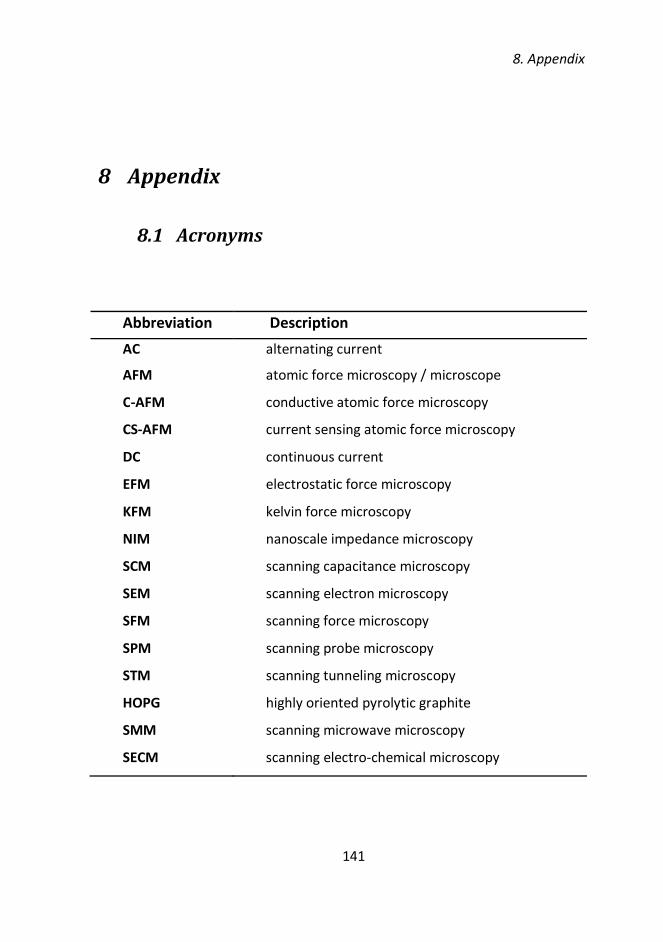
8. Appendix
141
8 Appendix
8.1 Acronyms
Abbreviation Description
AC alternating current
AFM atomic force microscopy / microscope
C-AFM conductive atomic force microscopy
CS-AFM current sensing atomic force microscopy
DC continuous current
EFM electrostatic force microscopy
KFM kelvin force microscopy
NIM nanoscale impedance microscopy
SCM scanning capacitance microscopy
SEM scanning electron microscopy
SFM scanning force microscopy
SPM scanning probe microscopy
STM scanning tunneling microscopy
HOPG highly oriented pyrolytic graphite
SMM scanning microwave microscopy
SECM scanning electro-chemical microscopy
142
8.2 Publications
G. Gramse, I. Casuso, J. Toset, L. Fumagalli and G. Gomila
Quantitative dielectric constant measurement of thin films by DC electrostatic
force microscopy
Nanotechnology 20, 395702, 2009
L. Fumagalli, G. Gramse, D. Esteban-Ferrer, M. A. Edwards, and G. Gomila
Quantifying the dielectric constant of thick insulators using electrostatic force
microscopy
Applied Physics Letters 96, 183107, 2010
G. Gramse, G. Gomila and L. Fumagalli
Quantifying the dielectric constant of thick insulators by electrostatic force
microscopy: Effects of the microscopic parts of the probe
Nanotechnology 23, 205703, 2012
G. Gramse, A. Dols, M. A. Edwards, L. Fumagalli and G. Gomila
Nanoscale polarization properties of biomembranes imaged and quantified in
electrolytic solution
In preparation
L. Fumagalli, G. Gramse, A. Dols and G. Gomila
Quantitative nanoscale dielectric microscopy of nanoparticles and
biomembranes on thick insulating substrates
In preparation
L. Fumagalli, G. Gramse and G. Gomila
Quantification of electrostatic force microscopy measurements with sharpened
probes for high spatial resolution dielectric characterization
In preparation
8. Appendix
143
8.3 Acknowledgements
I would like to thank all those who collaborated in a direct or indirect way
in this work.
I especially want to express my thanks to my supervisor Gabriel Gomila
guiding me all these years and contributing to this fruitful work.
Thanks also to all my group members for the good working atmosphere
and constructive and motivating talks about scientific topics and non-scientific
ones. I am especially grateful to Martin Edwards who spent lots of hours with
me sharing his knowledge about electrochemistry and finite element
simulations.
I also want to express my gratitude to all the external collaborators that
helped me on my way who were amongst others Juan Manuel Artés and the
group of Manel Puig.
Thanks to all my friends for their support, many of them I also found in
IBEC.
Over all, my thank goes to my family, Gemma and Joana who gave me the
love and energy to reach this point.
144
8.4 References
1. Binnig, G.; Rohrer, H.; Gerber, C.; Weibel, E. Physical Review Letters 1982, 49, (1), 57-61.
2. Binnig, G.; Rohrer, H., SCANNING TUNNELING MICROSCOPY. In 1986; Vol. 30, pp 355-369.
3. Binnig, G.; Quate, C. F.; Gerber, C. Physical Review Letters 1986, 56, (9), 930-933.
4. Umeda, N.; Ishizaki, S.; Uwai, H. Journal of Vacuum Science & Technology B 1991, 9, (2), 1318-1322.
5. Kim, G. M.; Kawai, S.; Nagashio, M.; Kawakatsu, H.; Brugger, J. Journal of Vacuum Science & Technology B 2004, 22, (4), 1658-1661.
6. Hantschel, T.; Niedermann, P.; Trenkler, T.; Vandervorst, W. Applied Physics Letters 2000, 76, (12), 1603-1605.
7. De Wolf, P.; Geva, M.; Hantschel, T.; Vandervorst, W.; Bylsma, R. B. Applied Physics Letters 1998, 73, (15), 2155-2157.
8. Eyben, P.; Xu, M.; Duhayon, N.; Clarysse, T.; Callewaert, S.; Vandervorst, W. Journal of Vacuum Science & Technology B 2002, 20, (1), 471-478.
9. Matey, J. R.; Blanc, J. Journal of Applied Physics 1985, 57, (5), 1437-1444. 10. Barrett, R. C.; Quate, C. F. Journal of Applied Physics 1991, 70, (5), 2725-
2733. 11. Shao, R.; Kalinin, S. V.; Bonnell, D. A. Applied Physics Letters 2003, 82, (12),
1869-1871. 12. O'Hayre, R.; Lee, M.; Prinz, F. B. Journal of Applied Physics 2004, 95, (12),
8382-8392. 13. Lee, D. T.; Pelz, J. P.; Bhushan, B., Scanning capacitance microscopy for thin
film measurements. In 2006; Vol. 17, pp 1484-1491. 14. Pingree, L. S. C.; Hersam, M. C. Applied Physics Letters 2005, 87, (23). 15. Fumagalli, L.; Ferrari, G.; Sampietro, M.; Casuso, I.; Martinez, E.; Samitier, J.;
Gomila, G. Nanotechnology 2006, 17, (18), 4581-4587. 16. Casuso, I.; Fumagalli, L.; Gomila, G.; Padros, E. Applied Physics Letters 2007,
91, (6), 3. 17. Fumagalli, L.; Ferrari, G.; Sampietro, M.; Gomila, G. Applied Physics Letters
2007, 91, (24). 18. Gomila, G.; Toset, J.; Fumagalli, L. Journal of Applied Physics 2008, 104, (2),
024315-024315-8. 19. Fumagalli, L.; Ferrari, G.; Sampietro, M.; Gomila, G. Nano Letters 2009, 9,
(4), 1604-1608. 20. Ferrari, G.; Sampietro, M. Review of Scientific Instruments 2007, 78, (9),
094703.
8. Appendix
145
21. Lai, K.; Ji, M. B.; Leindecker, N.; Kelly, M. A.; Shen, Z. X. Review of Scientific Instruments 2007, 78, (6).
22. Anlage, S.; Talanov, V.; Schwartz, A., Prinziples of Near-Field Microwave Microscopy. In Scanning probe microscopy: Electrical and Electromechanical Phenomena at the Nanoscale, Kalinin, S. V.; Gruverman, A., Eds. Springer: New York, 2006.
23. Gao, C.; Wei, T.; Duewer, F.; Lu, Y. L.; Xiang, X. D. Applied Physics Letters 1997, 71, (13), 1872-1874.
24. Tabib-Azar, M.; Wang, Y. Q. Ieee Transactions on Microwave Theory and Techniques 2004, 52, (3), 971-979.
25. Huber, H. P.; Moertelmaier, M.; Wallis, T. M.; Chiang, C. J.; Hochleitner, M.; Imtiaz, A.; Oh, Y. J.; Schilcher, K.; Dieudonne, M.; Smoliner, J.; Hinterdorfer, P.; Rosner, S. J.; Tanbakuchi, H.; Kabos, P.; Kienberger, F. Review of Scientific Instruments 2010, 81, (11).
26. Lai, K.; Kundhikanjana, W.; Kelly, M. A.; Shen, Z. X. Applied Physics Letters 2008, 93, (12).
27. Lai, K.; Kundhikanjana, W.; Kelly, M.; Shen, Z. X. Review of Scientific Instruments 2008, 79, (6).
28. Takeuchi, O.; Ohrai, Y.; Yoshida, S.; Shigekawa, H. Japanese Journal of Applied Physics Part 1-Regular Papers Brief Communications & Review Papers 2007, 46, (8B), 5626-5630.
29. Girard, P. Nanotechnology 2001, 12, (4), 485-490. 30. Garcia, R.; Perez, R. Surface Science Reports 2002, 47, (6-8), 197-301. 31. Cherniavskaya, O.; Chen, L. W.; Weng, V.; Yuditsky, L.; Brus, L. E. Journal
of Physical Chemistry B 2003, 107, (7), 1525-1531. 32. Nonnenmacher, M.; Oboyle, M. P.; Wickramasinghe, H. K. Applied Physics
Letters 1991, 58, (25), 2921-2923. 33. Knapp, H. F.; Mesquida, P.; Stemmer, A. Surface and Interface Analysis 2002, 33, (2), 108-112. 34. Goodman, T.; Bussmann, E.; Williams, C.; Taveras, M.; Britt, D. Langmuir
2004, 20, (9), 3684-3689. 35. Datta, S. S.; Strachan, D. R.; Mele, E. J.; Johnson, A. T. C. 2009, 9, (1), 7-11. 36. Meoded, T.; Shikler, R.; Fried, N.; Rosenwaks, Y. Applied Physics Letters
1999, 75, (16), 2435-2437. 37. Shikler, R.; Fried, N.; Meoded, T.; Rosenwaks, Y. Physical Review B 2000,
61, (16), 11041-11046. 38. Hu, J.; Xiao, X. D.; Salmeron, M. Applied Physics Letters 1995, 67, (4), 476-
478. 39. Salmeron, M.; Xu, L.; Hu, J.; Dai, Q. Mrs Bulletin 1997, 22, (8), 36-41. 40. Verdaguer, A.; Sacha, G. M.; Bluhm, H.; Salmeron, M. Chemical Reviews
2006, 106, (4), 1478-1510. 41. Hu, J.; Xiao, X. D.; Ogletree, D. F.; Salmeron, M. Surface Science 1995, 344,
(3), 221-236. 42. Hu, J.; Xiao, X. D.; Ogletree, D. F.; Salmeron, M. Science 1995, 268, (5208),
267-269. 43. Hu, J.; Xiao, X. D.; Ogletree, D. F.; Salmeron, M. Surface Science 1995, 327,
(3), 358-370.
146
44. Bard, A. J.; Faulkner, L. R., Electrochemical Methods: Fundamentals and Applications. 2nd Revised edition ed.; 2001.
45. von Helmholtz, H. L. F. Annalen der Physik 1853, 89, (211). 46. Chapman, D. L. Philosophical Magazine 1913, 25, (148), 475-481. 47. Bazant, M. Z.; Thornton, K.; Ajdari, A. Physical Review E 2004, 70, (2). 48. Kilic, M. S.; Bazant, M. Z.; Ajdari, A. Physical Review E 2007, 75, (2). 49. Kilic, M. S.; Bazant, M. Z.; Ajdari, A. Physical Review E 2007, 75, (2). 50. Olesen, L. H.; Bazant, M. Z.; Bruus, H. Physical Review E 2010, 82, (1). 51. Ludwig, M.; Kranz, C.; Schuhmann, W.; Gaub, H. E. Review of Scientific
Instruments 1995, 66, (4), 2857-2860. 52. Macpherson, J. V.; Unwin, P. R. Analytical Chemistry 2000, 72, (2), 276-285. 53. Eckhard, K.; Schuhmann, W. Analyst 2008, 133, (11), 1486-1497. 54. Kim, S.; Yoo, H.; Lee, K.; Friedman, B.; Gaspar, M. A.; Levicky, R. Applied
Physics Letters 2005, 86, (15). 55. Parsegia.Va; Gingell, D. Biophysical Journal 1972, 12, (9), 1192-&. 56. Israelachvili, J. N., Intermolecular and Surface Forces Third Edition ed.; 2011 57. Butt, H. J. Biophysical Journal 1991, 60, (4), 777-785. 58. Butt, H. J.; Cappella, B.; Kappl, M. Surface Science Reports 2005, 59, (1-6), 1-
152. 59. Pericet-Camara, R.; Papastavrou, G.; Behrens, S. H.; Borkovec, M. Journal of
Physical Chemistry B 2004, 108, (50), 19467-19475. 60. Butt, H. J. Biophysical Journal 1991, 60, (6), 1438-1444. 61. Raiteri, R.; Grattarola, M.; Butt, H. J. Journal of Physical Chemistry 1996,
100, (41), 16700-16705. 62. Doppenschmidt, A.; Butt, H. J. Colloids and Surfaces a-Physicochemical and
Engineering Aspects 1999, 149, (1-3), 145-150. 63. Hillier, A. C.; Kim, S.; Bard, A. J. Journal of Physical Chemistry 1996, 100,
(48), 18808-18817. 64. Giesbers, M.; Kleijn, J. M.; Stuart, M. A. C. Journal of Colloid and Interface
Science 2002, 248, (1), 88-95. 65. Wang, J.; Bard, A. J. Journal of Physical Chemistry B 2001, 105, (22), 5217-
5222. 66. Barten, D.; Kleijn, J. M.; Duval, J.; von Leeuwen, H. P.; Lyklema, J.; Stuart,
M. A. C. Langmuir 2003, 19, (4), 1133-1139. 67. Hu, K.; Fan, F. R. F.; Bard, A. J.; Hillier, A. C. Journal of Physical Chemistry
B 1997, 101, (41), 8298-8303. 68. Rentsch, S.; Siegenthaler, H.; Papastavrou, G. Langmuir 2007, 23, (17), 9083-
9091. 69. Yang, Y.; Mayer, K. M.; Hafner, J. H. Biophysical Journal 2007, 92, (6),
1966-1974. 70. Yang, Y.; Mayer, K. M.; Wickremasinghe, N. S.; Hafner, J. H. Biophysical
Journal 2008, 95, (11), 5193-5199. 71. Johnson, A. S.; Nehl, C. L.; Mason, M. G.; Hafner, J. H. Langmuir 2003, 19,
(24), 10007-10010. 72. Heinz, W. F.; Hoh, J. H. Biophysical Journal 1999, 76, (1), 528-538. 73. Sotres, J.; Baro, A. M. Applied Physics Letters 2008, 93, (10).
8. Appendix
147
74. Hirata, Y.; Mizutani, F.; Yokoyama, H. Surface and Interface Analysis 1999, 27, (5-6), 317-323.
75. Raiteri, R.; Butt, H. J. Journal of Physical Chemistry 1995, 99, (43), 15728-15732.
76. Umeda, K.-i.; Oyabu, N.; Kobayashi, K.; Hirata, Y.; Matsushige, K.; Yamada, H. Applied Physics Express 2010, 3, (6).
77. Kobayashi, N.; Asakawa, H.; Fukuma, T. Review of Scientific Instruments 2010, 81, (12).
78. Kao, K. C., Dielectric Phenomena in Solids. 2004. 79. Erlandsson, R.; McClelland, G. M.; Mate, C. M.; Chiang, S. Journal of
Vacuum Science & Technology a-Vacuum Surfaces and Films 1988, 6, (2), 266-270.
80. Hudlet, S.; Saint Jean, M.; Guthmann, C.; Berger, J. The European Physical Journal B - Condensed Matter and Complex Systems 1998, 2, (1), 5-10.
81. Krayev, A. V.; Talroze, R. V. Polymer 2004, 45, (24), 8195-8200. 82. Krayev, A. V.; Shandryuk, G. A.; Grigorov, L. N.; Talroze, R. V.
Macromolecular Chemistry and Physics 2006, 207, (11), 966-969. 83. Lu, W.; Wang, D.; Chen, L. W. Nano Letters 2007, 7, 2729-2733. 84. Smythy, Static and Dynamic Electricity. McGraw-Hill: New York, 1968. 85. Sacha, G. M.; Sahagun, E.; Saenz, J. J. Journal of Applied Physics 2007, 101,
(2), 024310-024310-4. 86. Sacha, G. M.; Saenz, J. J. Applied Physics Letters 2004, 85, (13), 2610-2612. 87. Abraham, D. W.; Martin, Y.; Wickramasinghe, K. 1988, 897, 191-8. 88. Hao, H. W.; Baro, A. M.; Saenz, J. J. Journal of Vacuum Science &
Technology B 1991, 9, (2), 1323-1328. 89. Belaidi, S.; Girard, P.; Leveque, G. Journal of Applied Physics 1997, 81, (3),
1023-1030. 90. Law, B. M.; Rieutord, F. Physical Review B 2002, 66, (3). 91. Gramse, G.; Casuso, I.; Toset, J.; Fumagalli, L.; Gomila, G. Nanotechnology
2009, 20, (39). 92. Shen, Y. X.; Barnett, D. M.; Pinsky, P. M. Applied Physics Letters 2008, 92,
(13). 93. Coster, H. G. L. Journal of Biological Physics 2003, 29, (4), 363-399. 94. Stern, J. E.; Terris, B. D.; Mamin, H. J.; Rugar, D. Applied Physics Letters
1988, 53, (26), 2717-2719. 95. Kalinin, S. V.; Karapetian, E.; Kachanov, M. Physical Review B 2004, 70,
(18), 184101.1-184101.24. 96. Lynch, B. P.; Hilton, A. M.; Simpson, G. J. Biophysical Journal 2006, 91, (7),
2678-2686. 97. Cho, Y. S.; Kirihara, A.; Saeki, T. Review of Scientific Instruments 1996, 67,
(6), 2297-2303. 98. Gao, C.; Xiang, X. D. Review of Scientific Instruments 1998, 69, (11), 3846-
3851. 99. Krauss, T. D.; Brus, L. E. Physical Review Letters 1999, 83, (23), 4840. 100. Cherniavskaya, O.; Chen, L.; Weng, V.; Yuditsky, L.; Brus, L. E. Journal of
Physical Chemistry 2003, 107, (7), 1525-1531. 101. Staii, C.; Johnson, A. T.; Pinto, N. J. Nano Letters 2004, 4, (5), 859-862.
148
102. Crider, P. S.; Majewski, M. R.; Jingyun, Z.; Oukris, H.; Israeloff, N. E. Applied Physics Letters 2007, 91, (1), 013102.
103. Clausen, C. H.; Jensen, J.; Castillo, J.; Dimaki, M.; Svendsen, W. E. Nano Letters 2008, 8, (11), 4066-4069.
104. Lhernould, M. S.; Delchambre, A.; Régnier, S.; Lambert, P. Applied Surface Science 2007, 253, (14), 6203-6210.
105. Toset, J.; Casuso, I.; Samitier, J.; Gomila, G. Nanotechnology 2007, 18, (1), 015503.
106. Oesterhelt, D.; Stoeckenius, W. Proceedings of the National Academy of Sciences 1973, 70, (10), 2853-2857.
107. Ltd, C. R., Silica and Silicon Dioxide - Properties. 2008. 108. Gomez-Monivas, S.; Froufe, L. S.; Carminati, R.; Greffet, J. J.; Saenz, J. J.
Nanotechnology 2001, 12, (4), 496-499. 109. Hutter, J. L.; Bechhoefer, J. Review of Scientific Instruments 1993, 64, (7),
1868-1873. 110. Palacios-Lidon, E.; Colchero, J. Nanotechnology 2006, 17, 5491-5500. 111. Riedel, C.; Arinero, R.; Tordjeman, P.; Leveque, G.; Schwartz, G. A.; Alegria,
A.; Colmenero, J. Physical Review E 2010, 81, (1). 112. Riedel, C.; Sweeney, R.; Israeloff, N. E.; Arinero, R.; Schwartz, G. A.;
Alegria, A.; Tordjeman, P.; Colmenero, J. Applied Physics Letters 2010, 96, (21).
113. Shen, Y.; Barnett, D. M.; Pinsky, P. M. Engineering Analysis with Boundary Elements 2008, 32, (8), 682-691.
114. Sacha, G. M.; Cardellach, M.; Segura, J. J.; Moser, J.; Bachtold, A.; Fraxedas, J.; Verdaguer, A. Nanotechnology 2009, 20, (28).
115. Miccio, L. A.; Kummali, M. M.; Montemartini, P. E.; Oyanguren, P. A.; Schwartz, G. A.; Alegria, A.; Colmenero, J. Journal of Chemical Physics 2011, 135, (6).
116. Zhao, M.; Gu, X.; Lowther, S. E.; Park, C.; Jean, Y. C.; Nguyen, T. Nanotechnology 2010, 21, (22).
117. Mikamo-Satoh, E.; Yamada, F.; Takagi, A.; Matsumoto, T.; Kawai, T. Nanotechnology 2009, 20, (14).
118. Benitez, J. J.; de la Fuente, O. R.; Diez-Perez, I.; Sanz, F.; Salmeron, M. Journal of Chemical Physics 2005, 123, (10).
119. Sacha, G. M.; Gomez-Navarro, C.; Saenz, J. J.; Gomez-Herrero, J. Applied Physics Letters 2006, 89, (17).
120. Takagi, A.; Yamada, F.; Matsumoto, T.; Kawai, T. Nanotechnology 2009, 20, (36).
121. Gramse, G.; Gomila, G.; Fumagalli, L. Nanotechnology 2012, 23, (20), 205703.
122. Fumagalli, L.; Gramse, G.; Esteban-Ferrer, D.; Edwards, M. A.; Gomila, G. Applied Physics Letters 2010, 96, (18).
123. Fumagalli, L.; Gramse, G.; Dols-Peréz, A.; Gomila, G. in preparation. 124. Scheuring, S.; Seguin, J.; Marco, S.; Levy, D.; Robert, B.; Rigaud, J. L.
Proceedings of the National Academy of Sciences of the United States of America 2003, 100, (4), 1690-1693.
8. Appendix
149
125. Cross, S. E.; Jin, Y.-S.; Rao, J.; Gimzewski, J. K. Nature Nanotechnology 2007, 2, (12), 780-783.
126. Manne, S.; Hansma, P. K.; Massie, J.; Elings, V. B.; Gewirth, A. A. Science 1991, 251, (4990), 183-186.
127. Rico, F.; Su, C.; Scheuring, S. Nano Letters 2011, 11, (9), 3983-3986. 128. Alonso, J. L.; Goldmann, W. H. Life Sciences 2003, 72, (23), 2553-2560. 129. Ivanovska, I. L.; de Pablo, P. J.; Ibarra, B.; Sgalari, G.; MacKintosh, F. C.;
Carrascosa, J. L.; Schmidt, C. F.; Wuite, G. J. L. Proceedings of the National Academy of Sciences of the United States of America 2004, 101, (20), 7600-7605.
130. Wittstock, G.; Burchardt, M.; Pust, S. E.; Shen, Y.; Zhao, C. Angewandte Chemie-International Edition 2007, 46, (10), 1584-1617.
131. Kalinin, S. V.; Bonnell, D. A. Physical Review B 2002, 65, (12). 132. Rodriguez, B. J.; Jesse, S.; Baddorf, A. P.; Kalinin, S. V. Physical Review
Letters 2006, 96, (23). 133. Lu, W.; Xiong, Y.; Hassanien, A.; Zhao, W.; Zheng, M.; Chen, L. Nano
Letters 2009, 9, (4), 1668-1672. 134. Sounart, T. L.; Panchawagh, H. V.; Mahajan, R. L. Applied Physics Letters
2010, 96, (20). 135. Malmivuo, J.; Plonsey, J. R., Bioelectromagnetism: principles and
applications of bioelectric and biomagnetic fields. Oxford University Press: New York, 1995.
136. Dilger, J. P.; McLaughlin, S. G. A.; McIntosh, T. J.; Simon, S. A. Science 1979, 206, (4423), 1196-1198.
137. Warshel, A.; Sharma, P. K.; Kato, M.; Parson, W. W., Modeling electrostatic effects in proteins. In 2006; Vol. 1764, pp 1647-1676.
138. van Meer, G.; Voelker, D. R.; Feigenson, G. W. Nature Reviews Molecular Cell Biology 2008, 9, (2), 112-124.
139. Huang, W.; Levitt, D. G., Theoretical Calculation Of Dielectric-Constant Of A Bilayer Membrane. In 1977; Vol. 17, pp 111-128.
140. Stern, H. A.; Feller, S. E. Journal of Chemical Physics 2003, 118, (7), 3401-3412.
141. Nymeyer, H.; Zhou, H.-X. Biophysical Journal 2008, 94, (4), 1185-1193. 142. Steinem, C.; Janshoff, A.; Ulrich, W. P.; Sieber, M.; Galla, H. J. Biochimica Et
Biophysica Acta-Biomembranes 1996, 1279, (2), 169-180.