Embed Size (px)
Citation preview

Lecture 5 Differential and Multistage Amplifiers
Thawatchai Thongleam
Program in Electronics Engineering
Faculty of Science and Technology
Nakhon Pathom Rajabhat University

Outline
• The BJT Differential Pair
• Small Signal Operation of The BJT Differential Amplifier
• Other Nonideal Differential Amplifier
• Biasing in BJT Integrated Circuit
• BJT Differential Amplifier
•MOS Differential Amplifiers
•Multistage Amplifiers
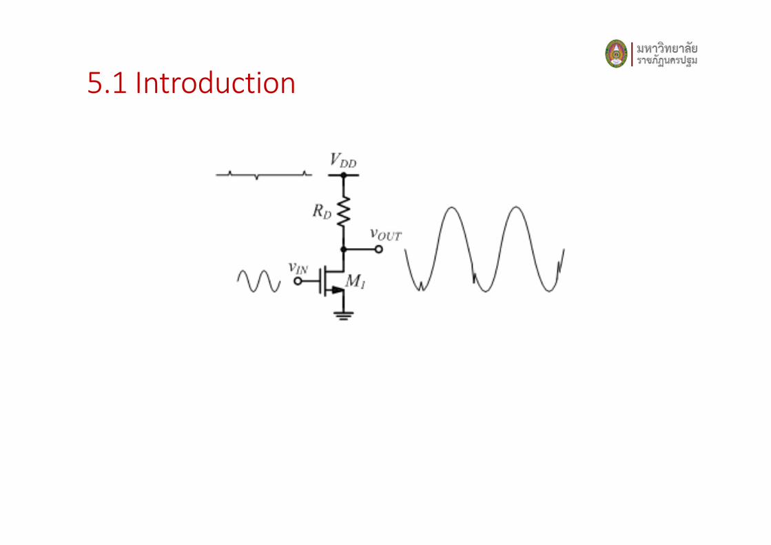
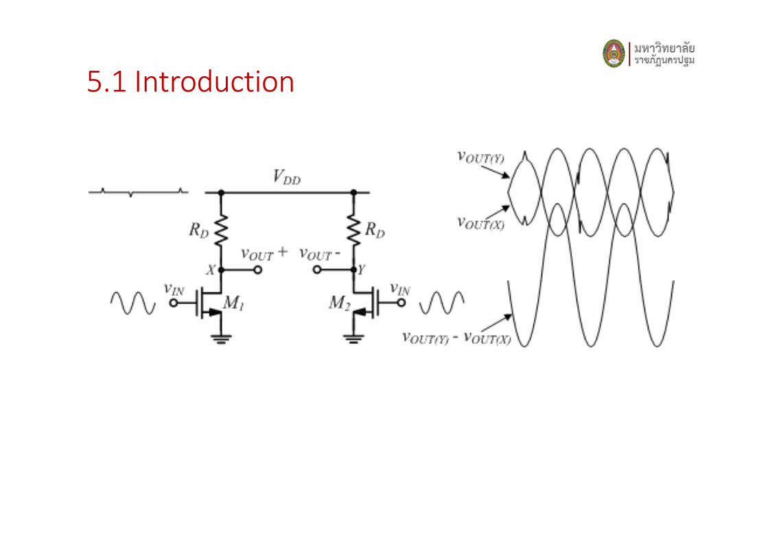
5.1 Introduction

5.1 Introduction
5.1 Introduction
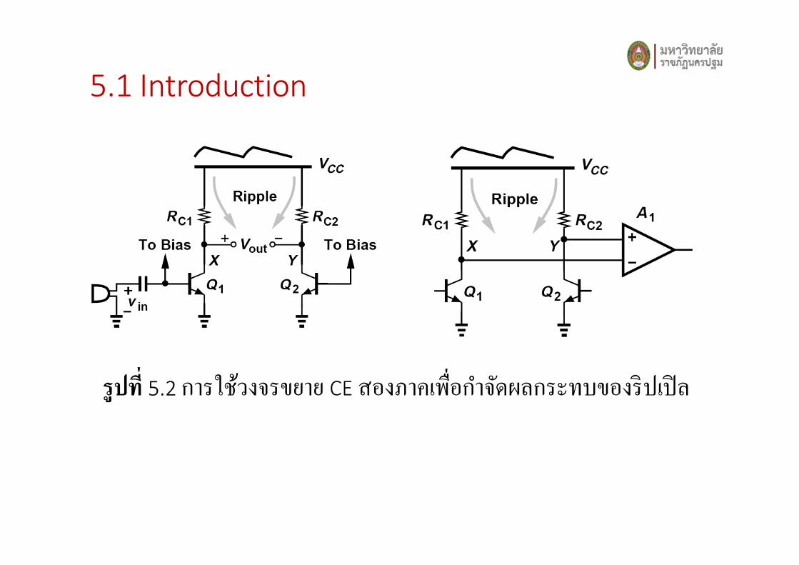
รูปที� 5.2 การใชว้งจรขยาย CE สองภาคเพื�อกาํจดัผลกระทบของริปเปิล
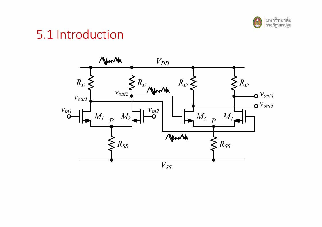
5.1 Introduction
5.1 Introduction
VSS
vin1
RD
M1 M2
vout1
RSS
RD
vout2
P
RD
VDD
M3 M4
vout3
RSS
RD
vout4
P
vin2
5.2 Signal
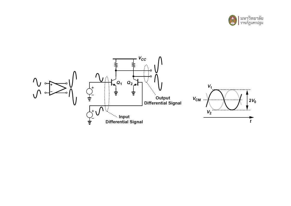
• สัญญาณโหมดผลต่าง (Differential mode signal) คือ ระดบัของสัญญาณที�วงจรที�มีค่าแตกต่างกนั
• สัญญาณโหมดร่วม (Common mode signal) คือ ระดบัของสัญญาณที�วงจรใชร้่วมกนั
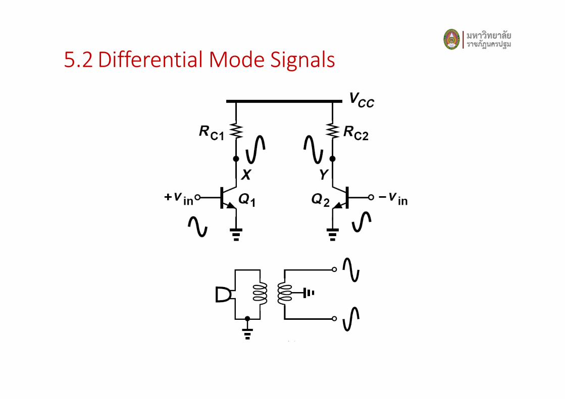
5.2 Differential Mode Signals
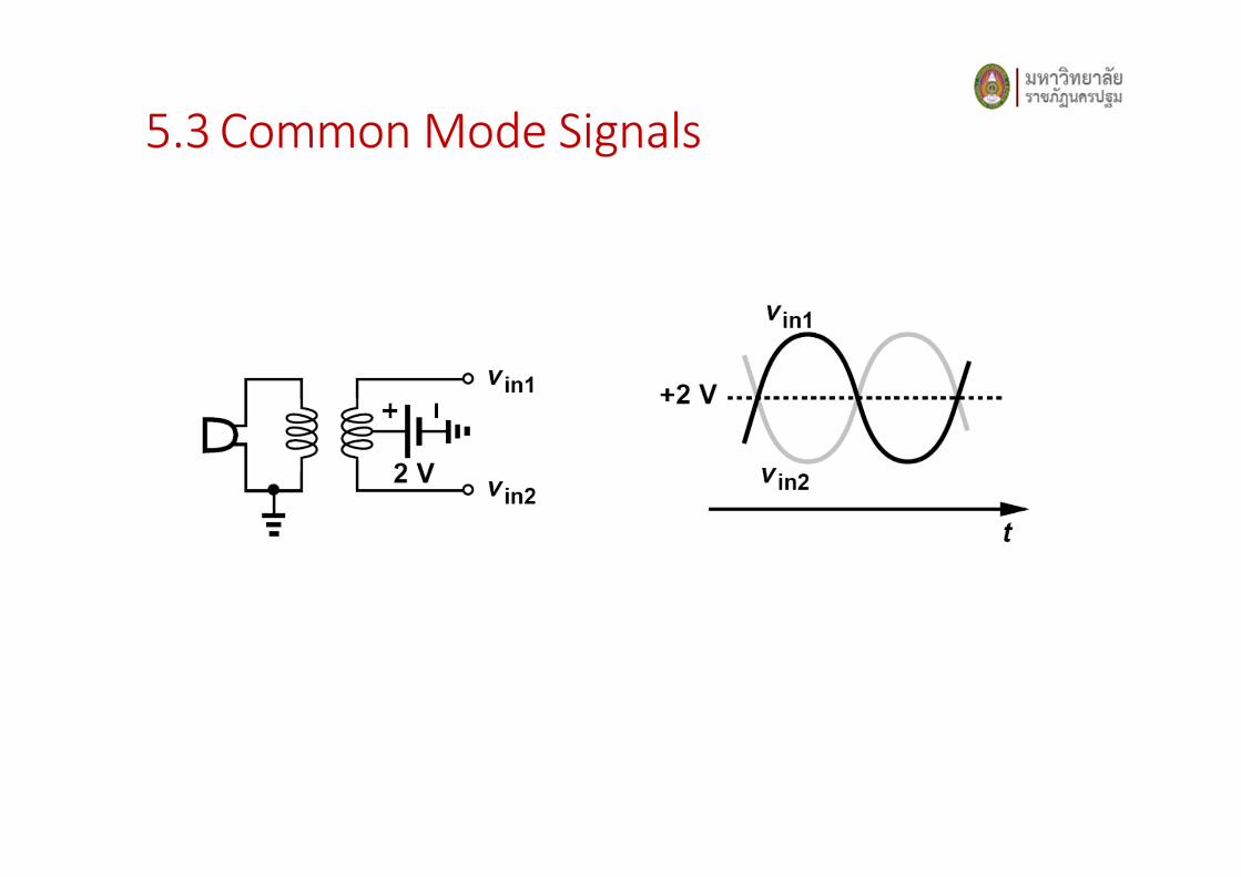
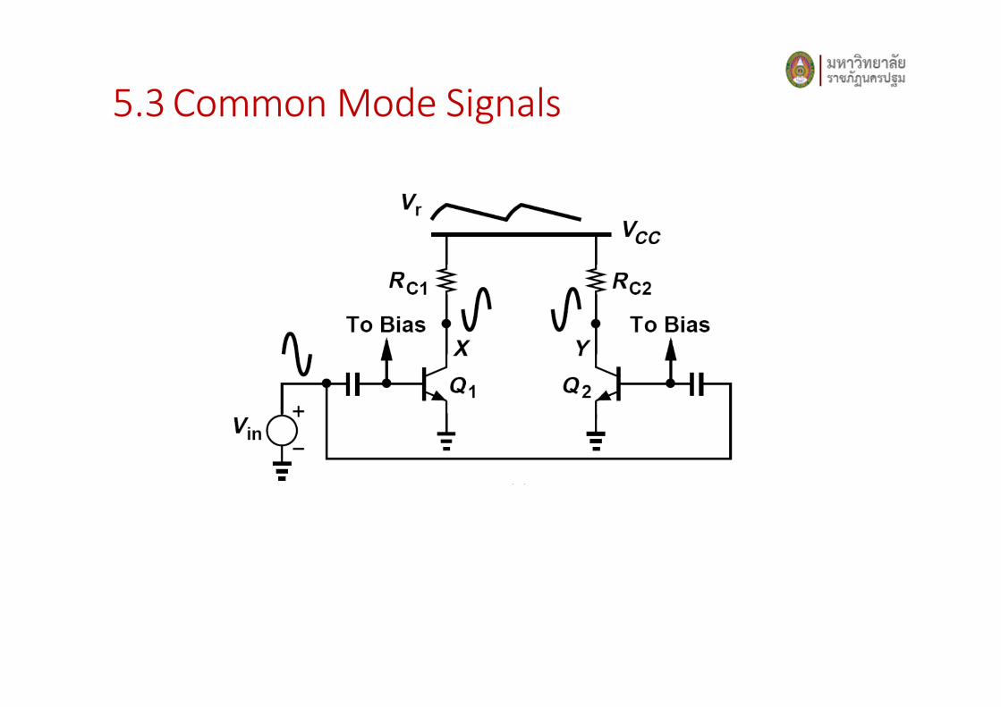
5.3 Common Mode Signals
5.3 Common Mode Signals

5.4 Differential pair
รูปที� 5.6 วงจรขยายคู่ผลต่าง (ก) ไบโพล่า (ข) มอสเฟต

5.5 Input CM Noise with Ideal Tail Current
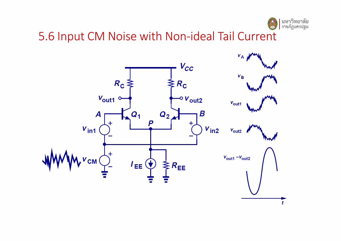
5.6 Input CM Noise with Non-ideal Tail Current

5.7 Comparison
• As it can be seen, the differential output voltages for both cases are the same. So for small input CM noise, the differential pair is not affected.
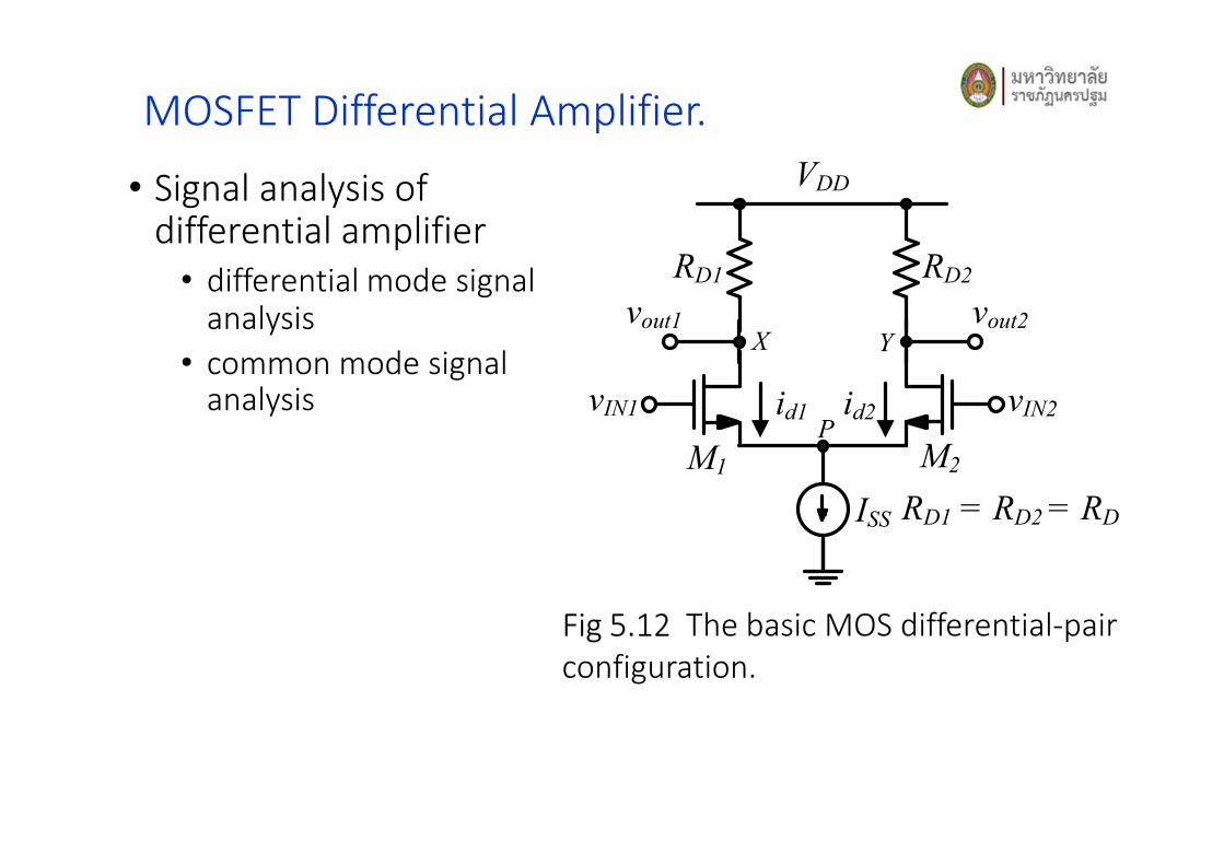
MOSFET Differential Amplifier.
• Signal analysis of differential amplifier
• differential mode signal analysis
• common mode signal analysis
Fig 5.12 The basic MOS differential-pair
configuration.
RD1
VDD
M1 M2
vout1
RD2
vout2
P
ISS
X Y
id1 id2vIN1 vIN2
RD1 = RD2 = RD
RD1
VDD
M1 M2
vout1
RD2
vout2
P
ISS
X Y
id1 id2vIN1 vIN2
RD1 = RD2 = RD
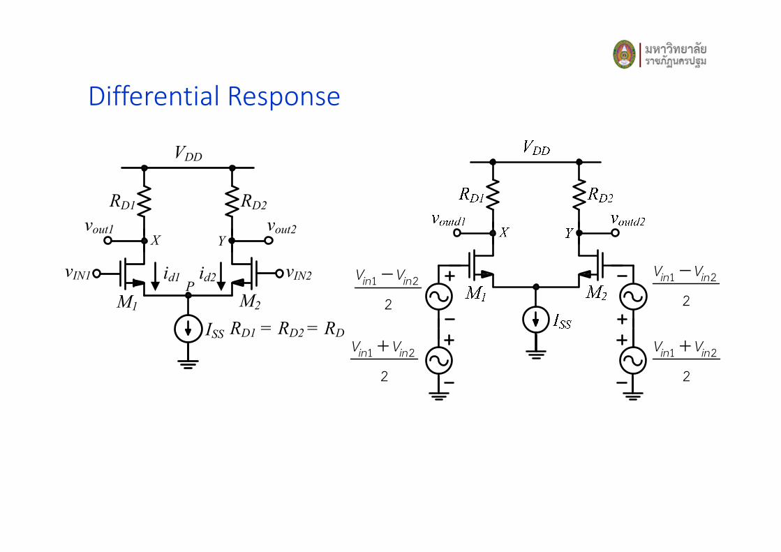
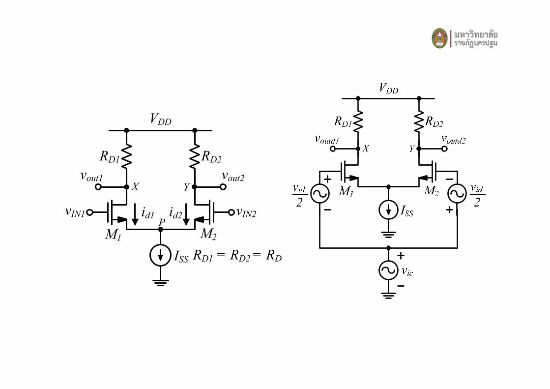
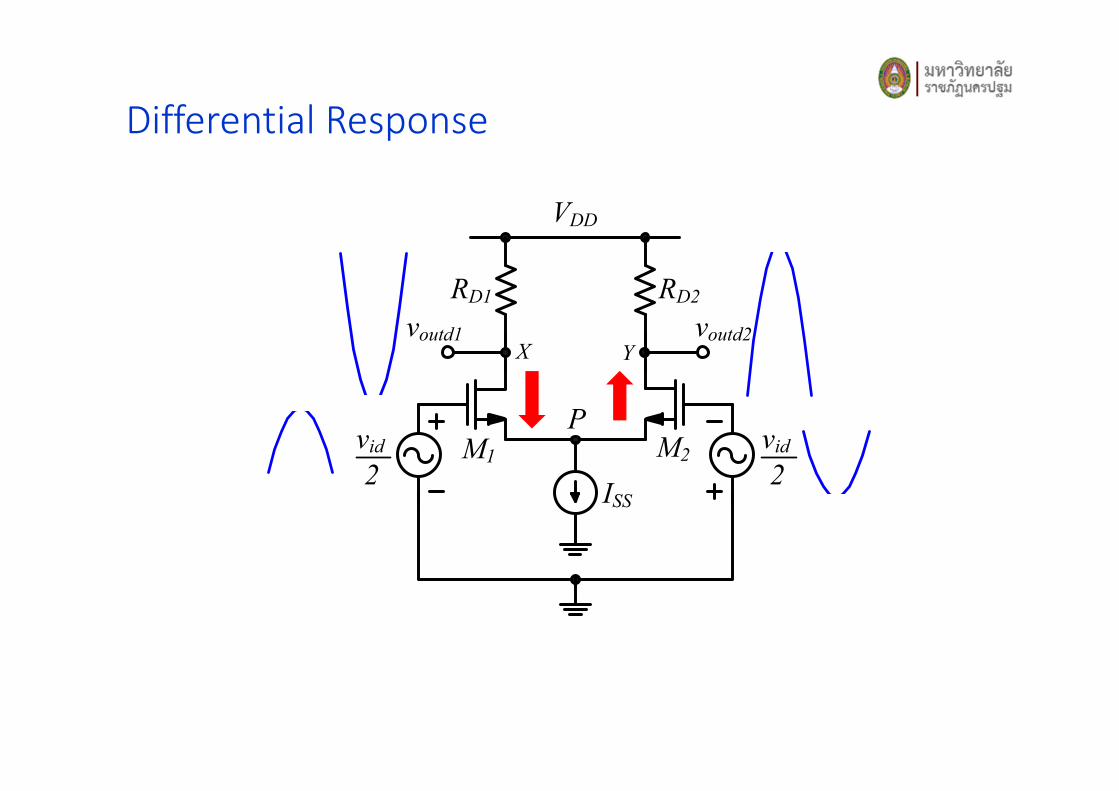
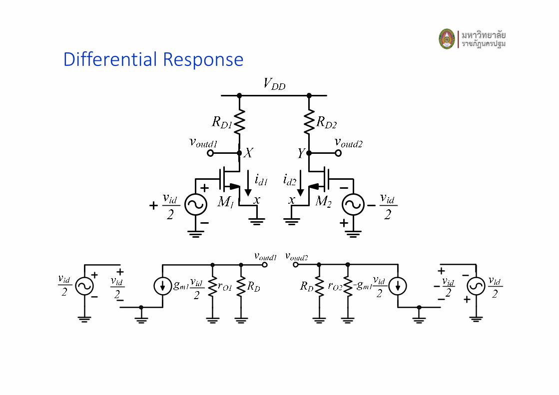
Differential Response
RD1
VDD
M1 M2
vout1
RD2
vout2
P
ISS
X Y
id1 id2vIN1 vIN2
RD1 = RD2 = RD
in inV V−1 2
2
in inV V−1 2
2
in inV V+1 2
2in inV V+1 2
2
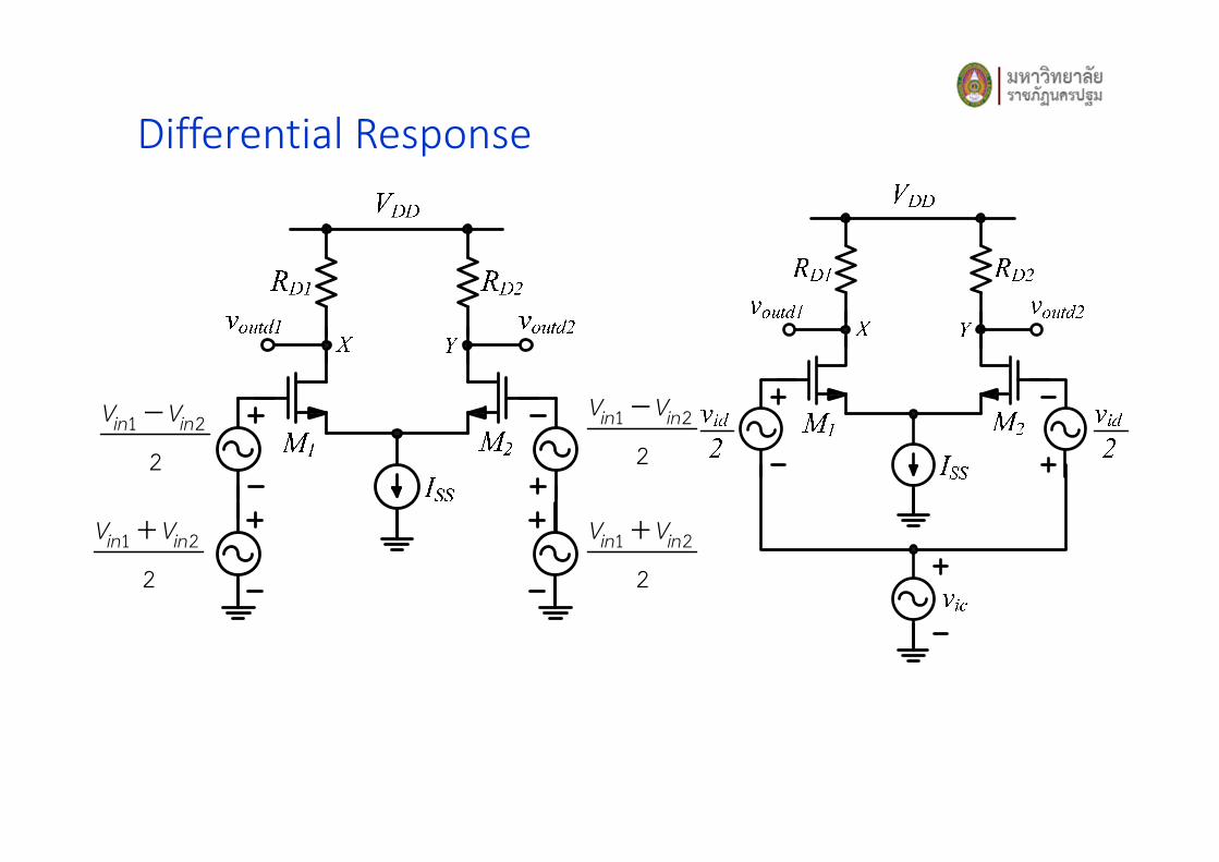
Differential Response
in inV V−1 2
2
in inV V−1 2
2
in inV V+1 2
2in inV V+1 2
2

Differential Response
RD1
VDD
M1 M2
voutd1
RD2
voutd2
ISS
X Y
vid
2
vid
2
RD1
VDD
M1 M2
voutc1
RD2
voutc2
ISS
X Y
vic

RD1
VDD
M1 M2
vout1
RD2
vout2
P
ISS
X Y
id1 id2vIN1 vIN2
RD1 = RD2 = RD

Differential Response
RD1
VDD
M1 M2
vout1
RD2
vout2
P
ISS
X Y
id1 id2vIN1 vIN2
RD1 = RD2 = RD
V∆
VIN1 – VIN2
ID
ISS
ID2
ISS
2
V∆−
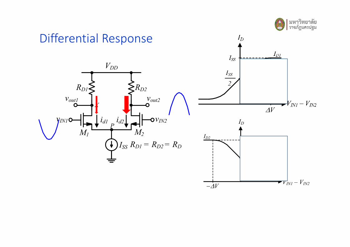
Differential Response
RD1
VDD
M1 M2
vout1
RD2
vout2
P
ISS
X Y
id1 id2vIN1 vIN2
RD1 = RD2 = RD
V∆
VIN1 – VIN2
ID
ISS
ID2
ISS
2
V∆−
Differential Response
RD1
VDD
M1 M2
vout1
RD2
vout2
P
ISS
X Y
id1 id2vIN1 vIN2
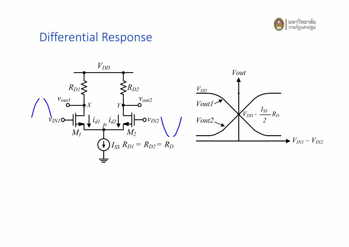
RD1 = RD2 = RDVIN1 – VIN2
VDD
Vout
Vout1
Vout2
ISS
2VDD - RD
Differential Response
RD1
VDD
M1 M2
vout1
RD2
vout2
P
ISS
X Y
id1 id2vIN1 vIN2
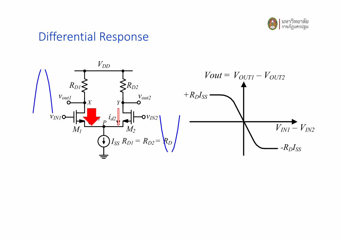
RD1 = RD2 = RD
VIN1 – VIN2
+RDISS
-RDISS
Vout = VOUT1 – VOUT2
Differential Response
RD1
VDD
M1 M2
voutd1
RD2
voutd2
ISS
X Y
vid
2
vid
2
P
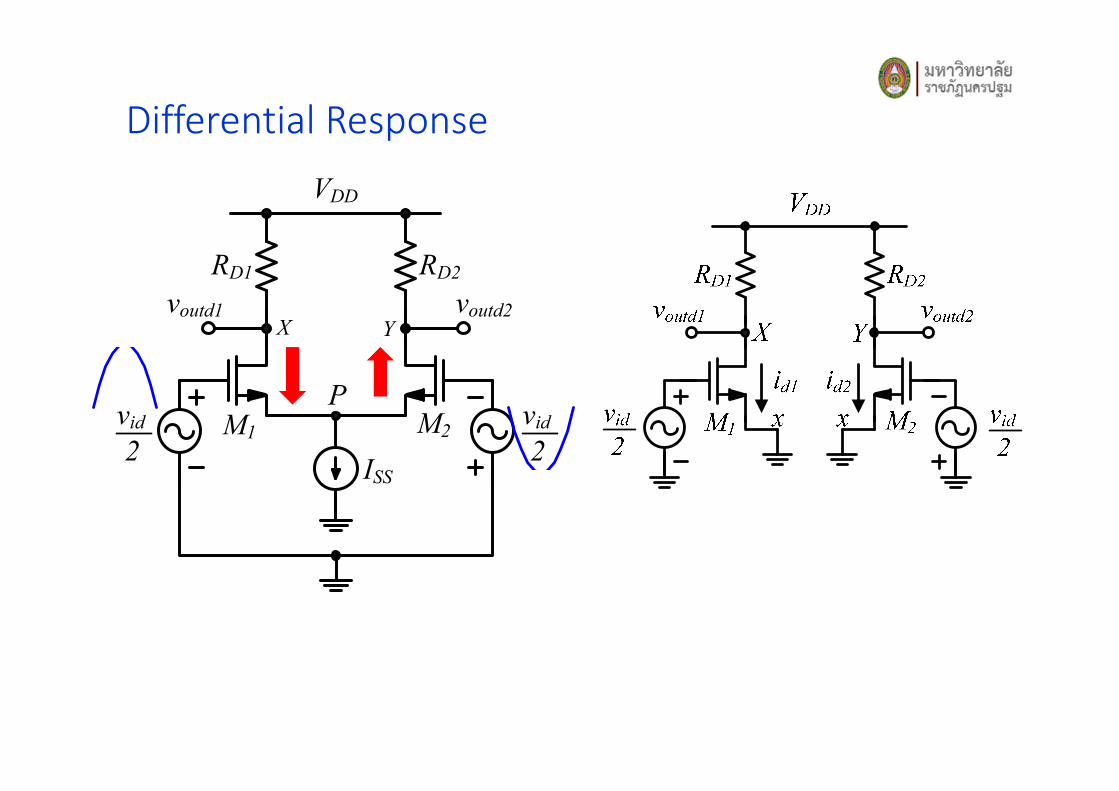
Differential Response
RD1
VDD
M1 M2
voutd1
RD2
voutd2
ISS
X Y
vid
2
vid
2
P
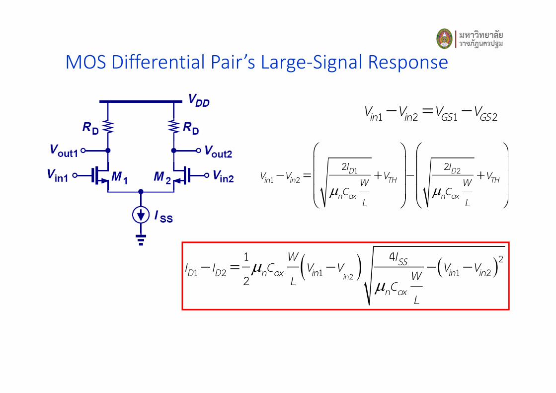
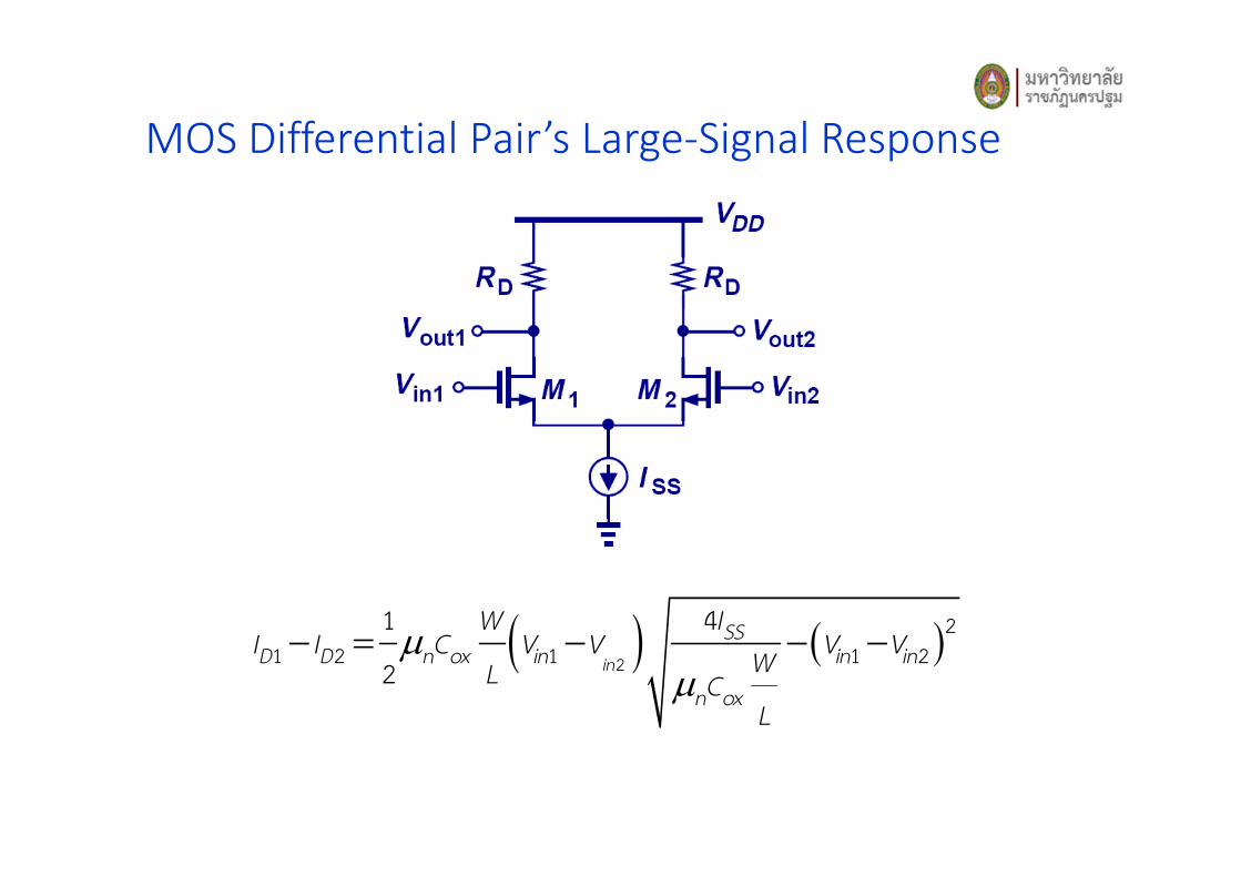
MOS Differential Pair’s Large-Signal Response
( ) ( )in
SSD D n ox in in in
n ox
W II I C V V V VWL C
L
µµ
− = − − −2
21 2 1 1 2
1 4
2
in in GS GSV V V V− = −1 2 1 2
1 21 2
2 2D Din in TH TH
n ox n ox
I IV V V VW W
C CL L
µ µ
− = + − +
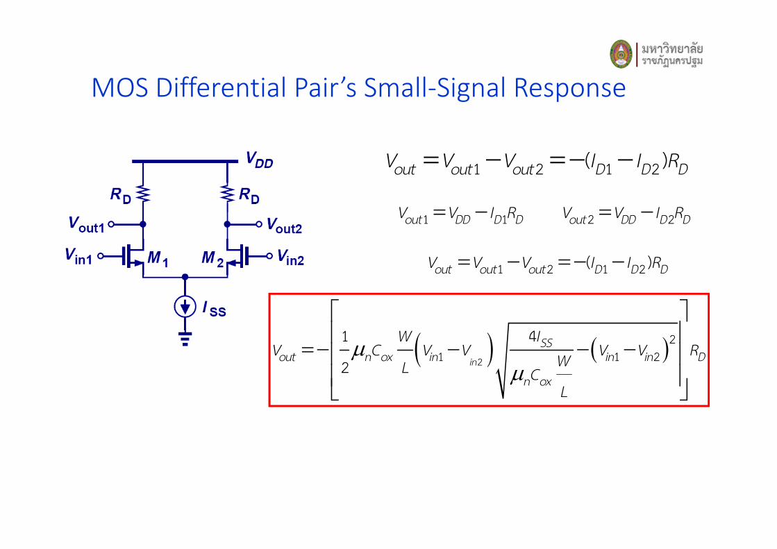
MOS Differential Pair’s Small-Signal Response
out out out D D DV V V I I R= − =− −1 2 1 2( )
out out out D D DV V V I I R= − =− −1 2 1 2( )
out DD D DV V I R= −1 1 out DD D DV V I R= −2 2
( ) ( )in
SSout n ox in in in D
n ox
W IV C V V V V RWL C
L
µµ
=− − − −
2
21 1 2
1 4
2
MOS Differential Pair’s Large-Signal Response
( ) ( )in
SSD D n ox in in in
n ox
W II I C V V V V
WL CL
µµ
− = − − −2
21 2 1 1 2
1 4
2
Differential Response
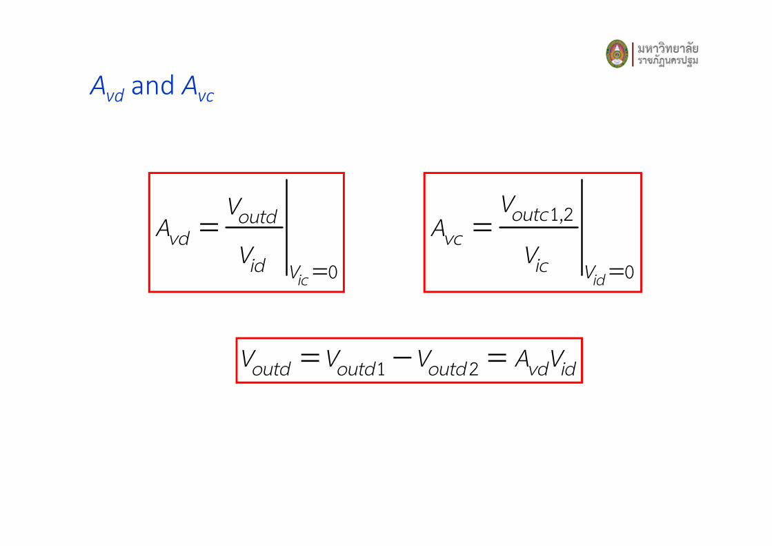
Avd
and Avc
0ic
outdvd
id V
VA
V =
=
outd outd outd vd idV V V A V= − =1 2
id
outcvc
ic V
VA
V =
= 1,2
0
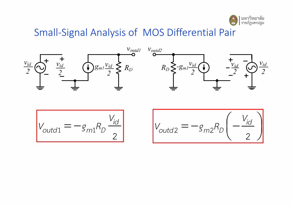
Small-Signal Analysis of MOS Differential Pair
1 12id
outd m DV
V g R= − 2 22id
outd m DV
V g R = − −
-gm1RD
voutd2
vid
2
vid
2
vid
2

Virtual Ground and Half Circuit
1 2m m m n ox SSW
g g g C IL
µ= = =
outdvd m D
id
VA g R
V= = −
outd outd outd m D idV V V g R V= − = −1 2
-gm1RD
voutd2
vid
2
vid
2
vid
2
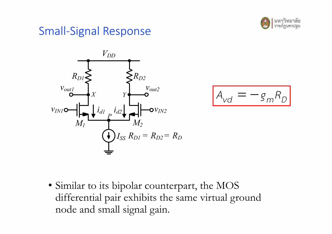
Small-Signal Response
• Similar to its bipolar counterpart, the MOS differential pair exhibits the same virtual ground node and small signal gain.
vd m DA g R= −RD1
VDD
M1 M2
vout1
RD2
vout2
P
ISS
X Y
id1 id2vIN1 vIN2
RD1 = RD2 = RD
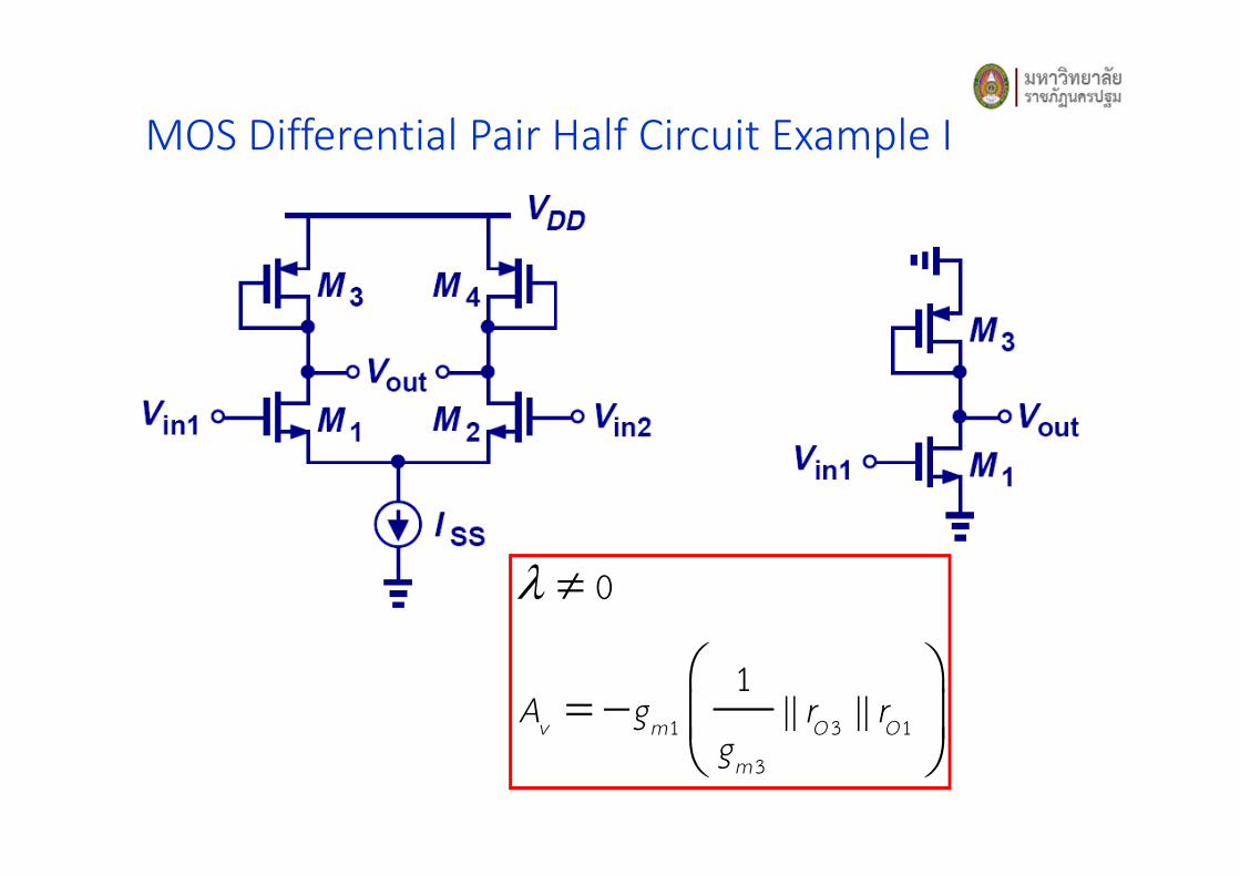
MOS Differential Pair Half Circuit Example I
1 3 1
3
0
1|| ||v m O O
m
A g r rg
λ ≠
= −
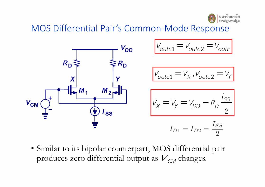
MOS Differential Pair’s Common-Mode Response
• Similar to its bipolar counterpart, MOS differential pair produces zero differential output as V
CMchanges.
SSX Y DD D
IV V V R= = −
2
outc outc outcV V V= =1 2
1 2outc X outc YV V ,V V= =
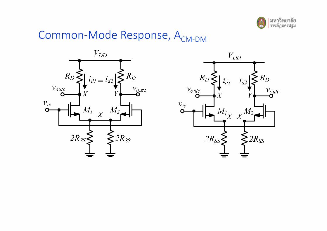
Common-Mode Response, ACM-DM
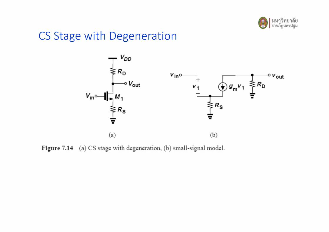
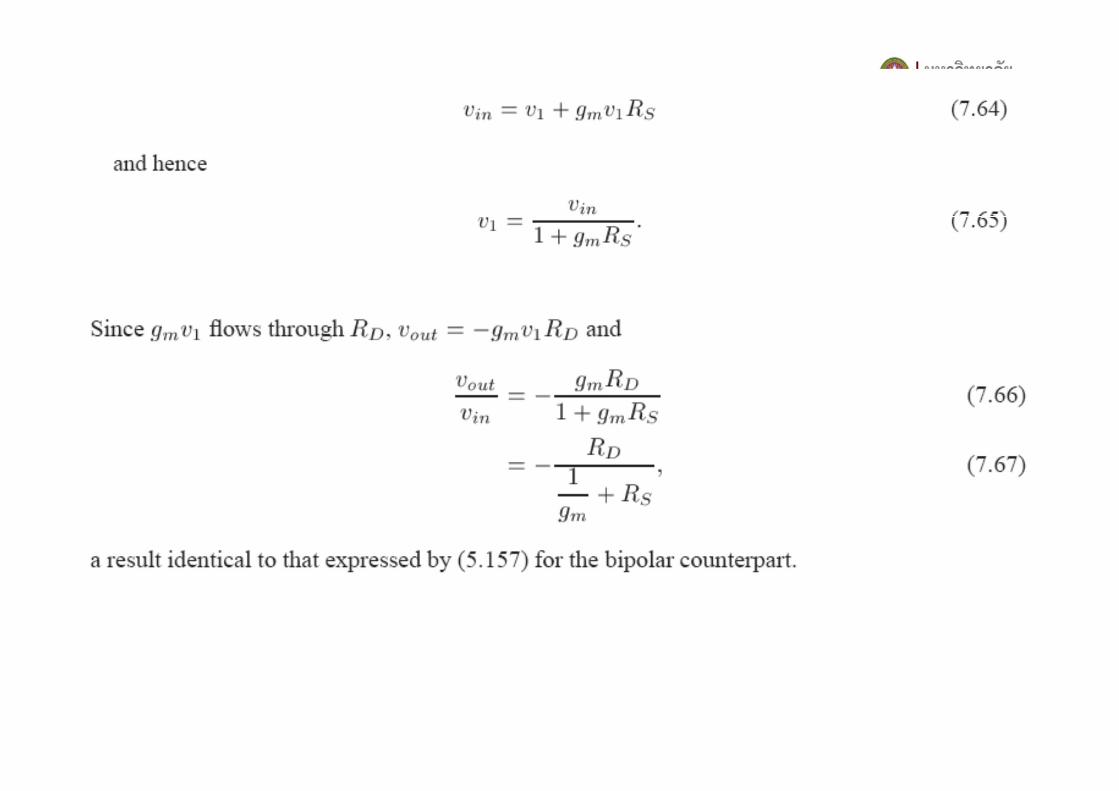
CS Stage with Degeneration

Common-Mode Response, ACM-DM
1 21 2
m Doutc outc ic
m SS
g RV V V
g R= ≅ −
+
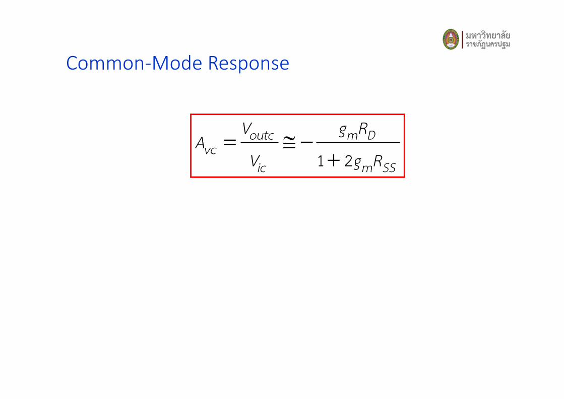
Common-Mode Response
1 2outc m D
vcic m SS
V g RA
V g R= ≅ −
+
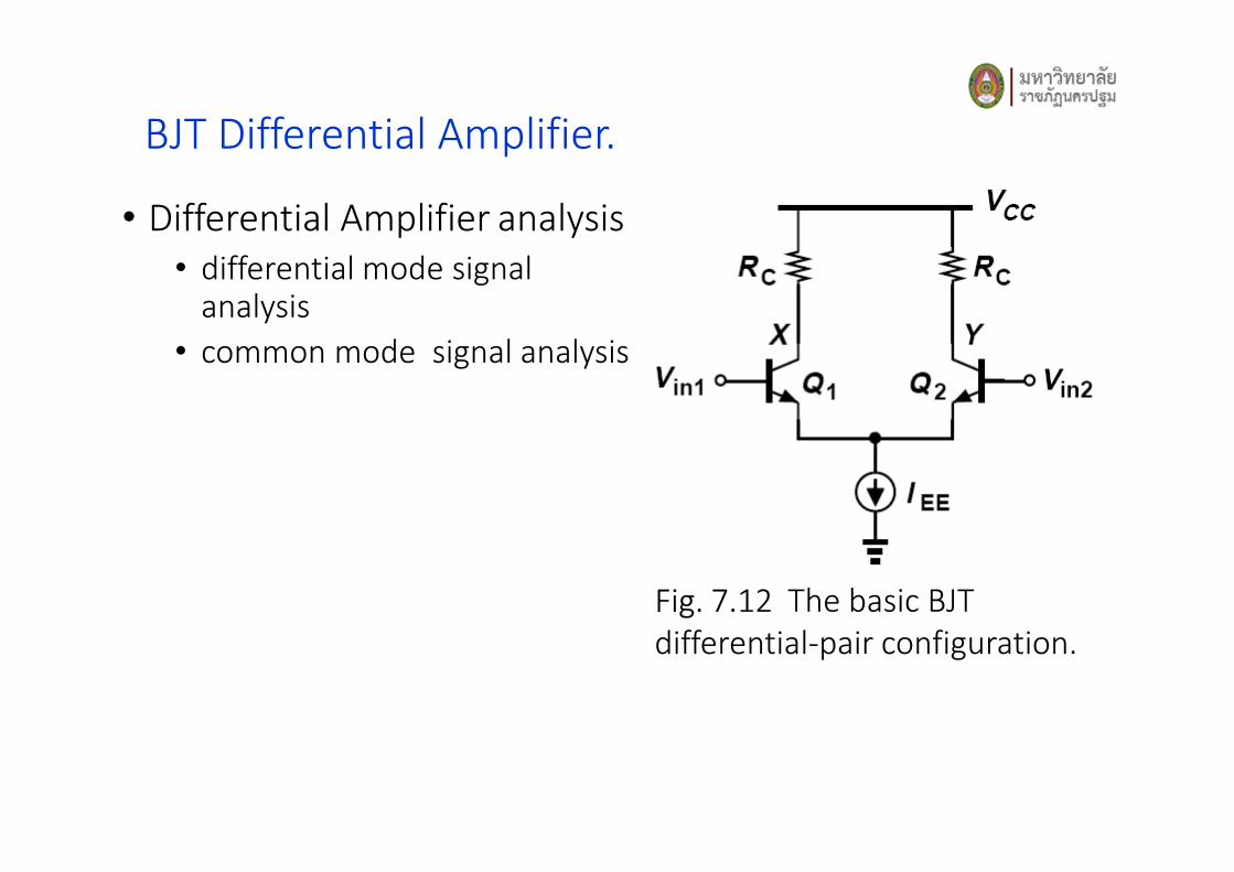
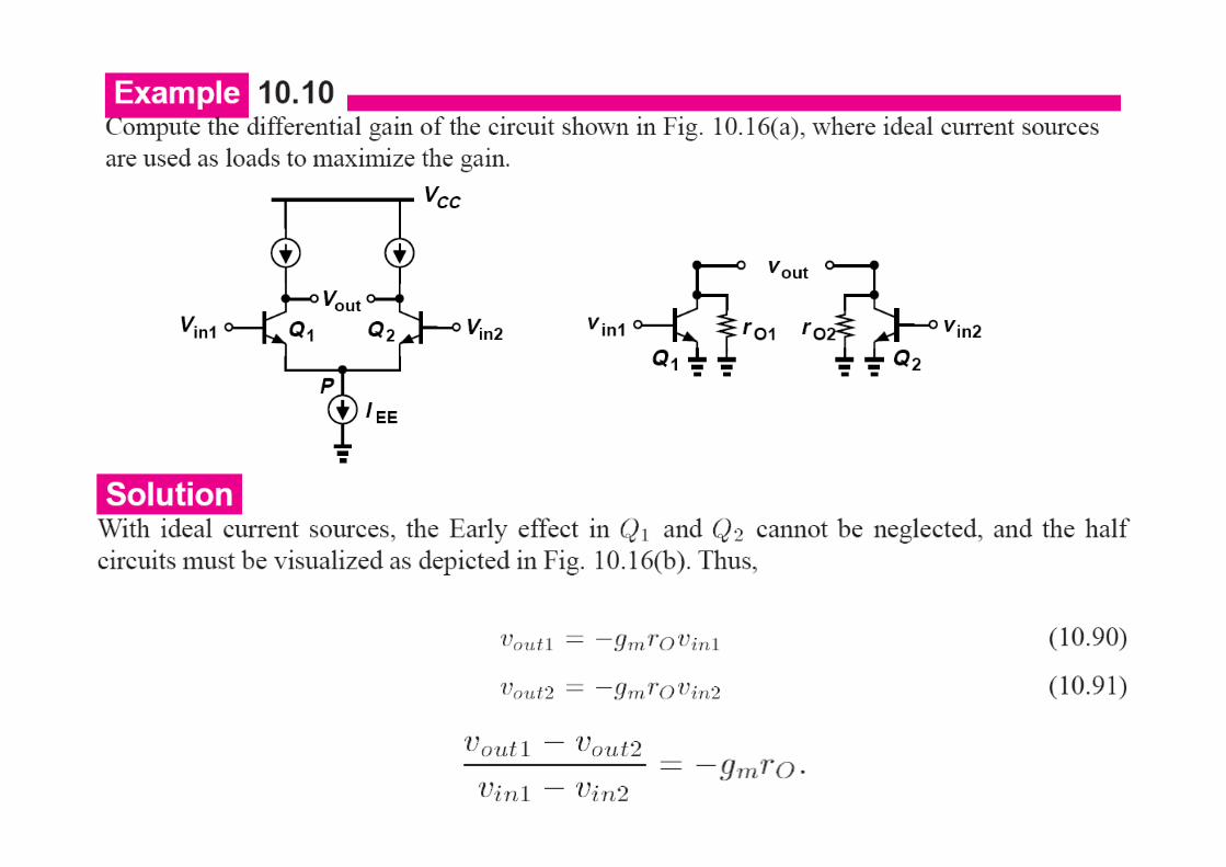
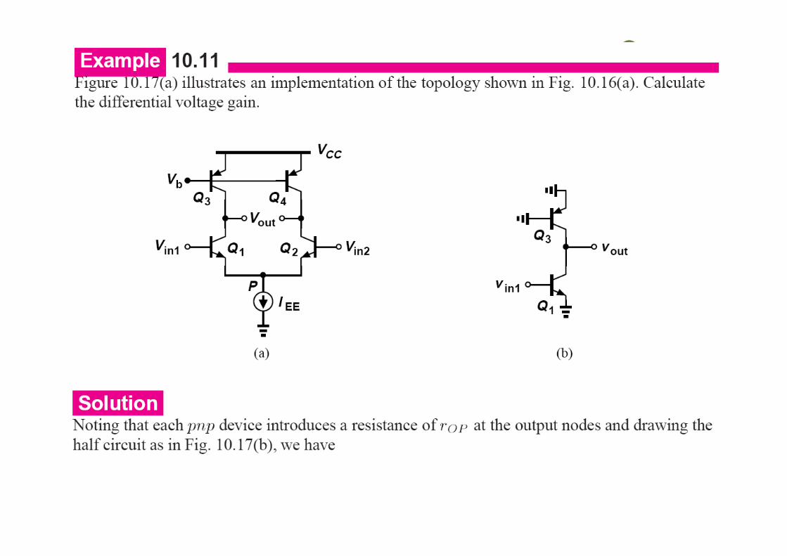
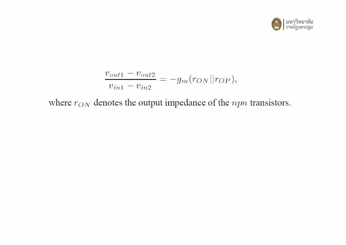
BJT Differential Amplifier.
• Differential Amplifier analysis • differential mode signal
analysis
• common mode signal analysis
Fig. 7.12 The basic BJT
differential-pair configuration.
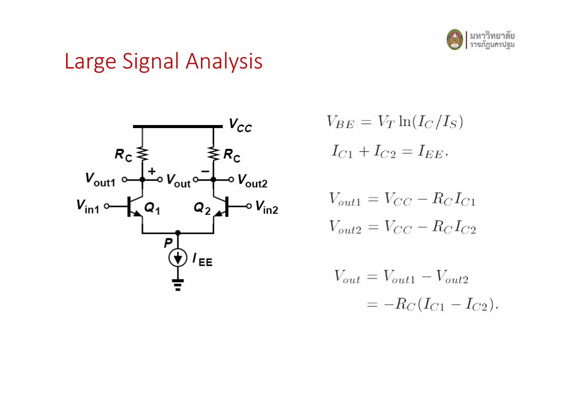
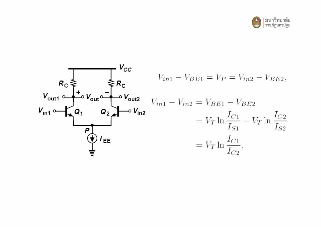
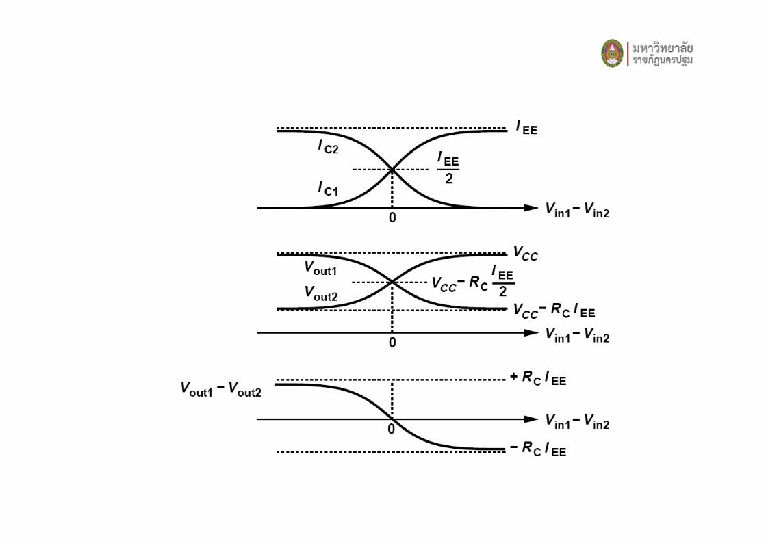
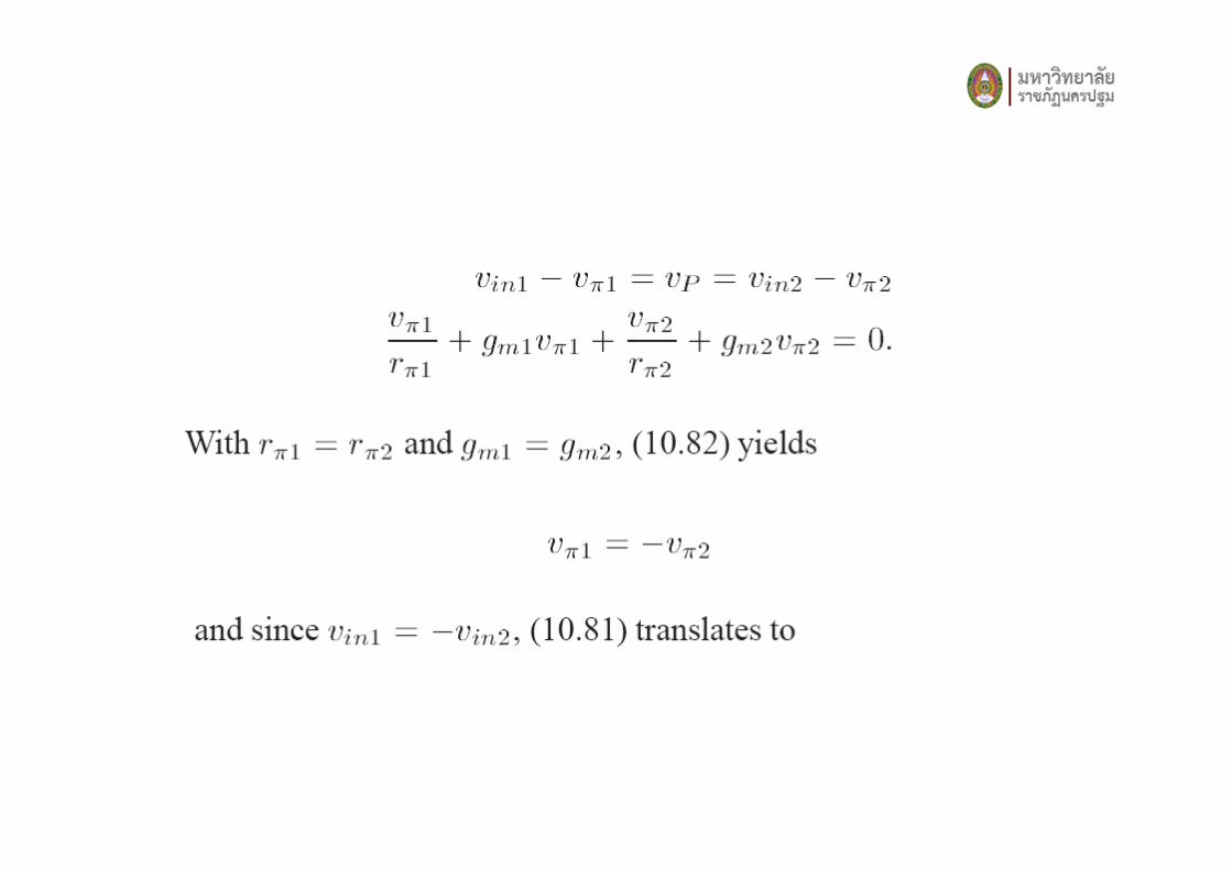
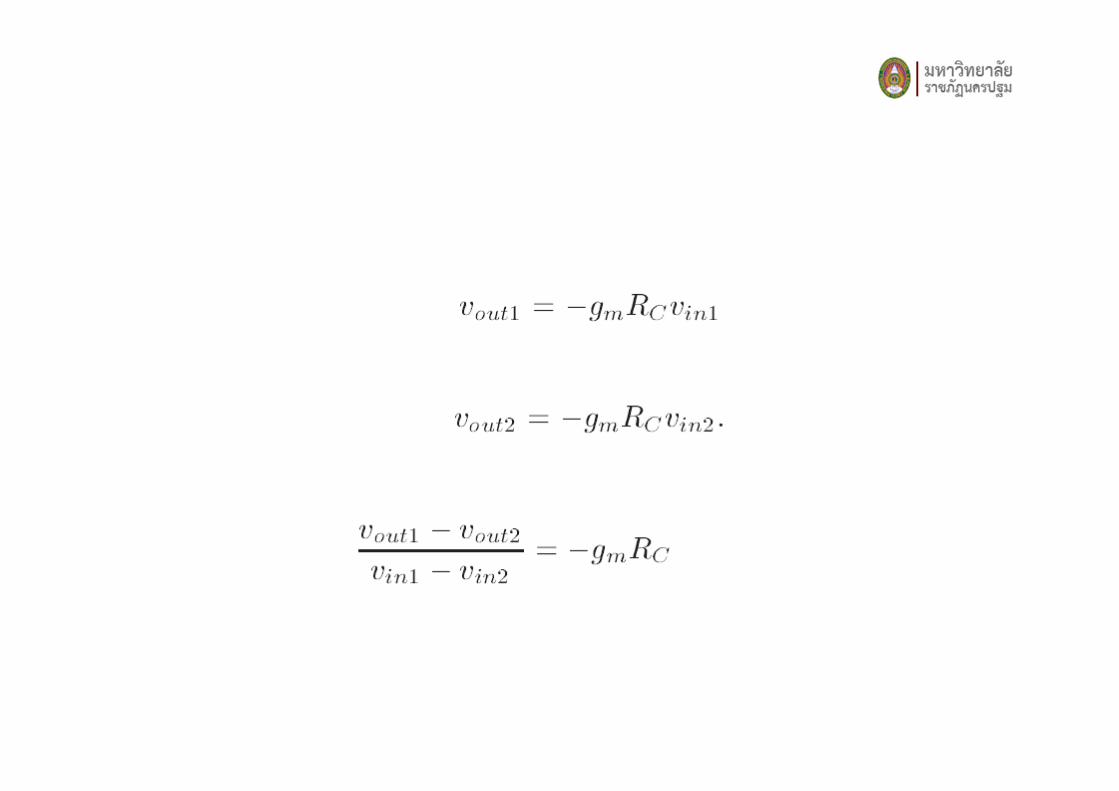
Large Signal Analysis
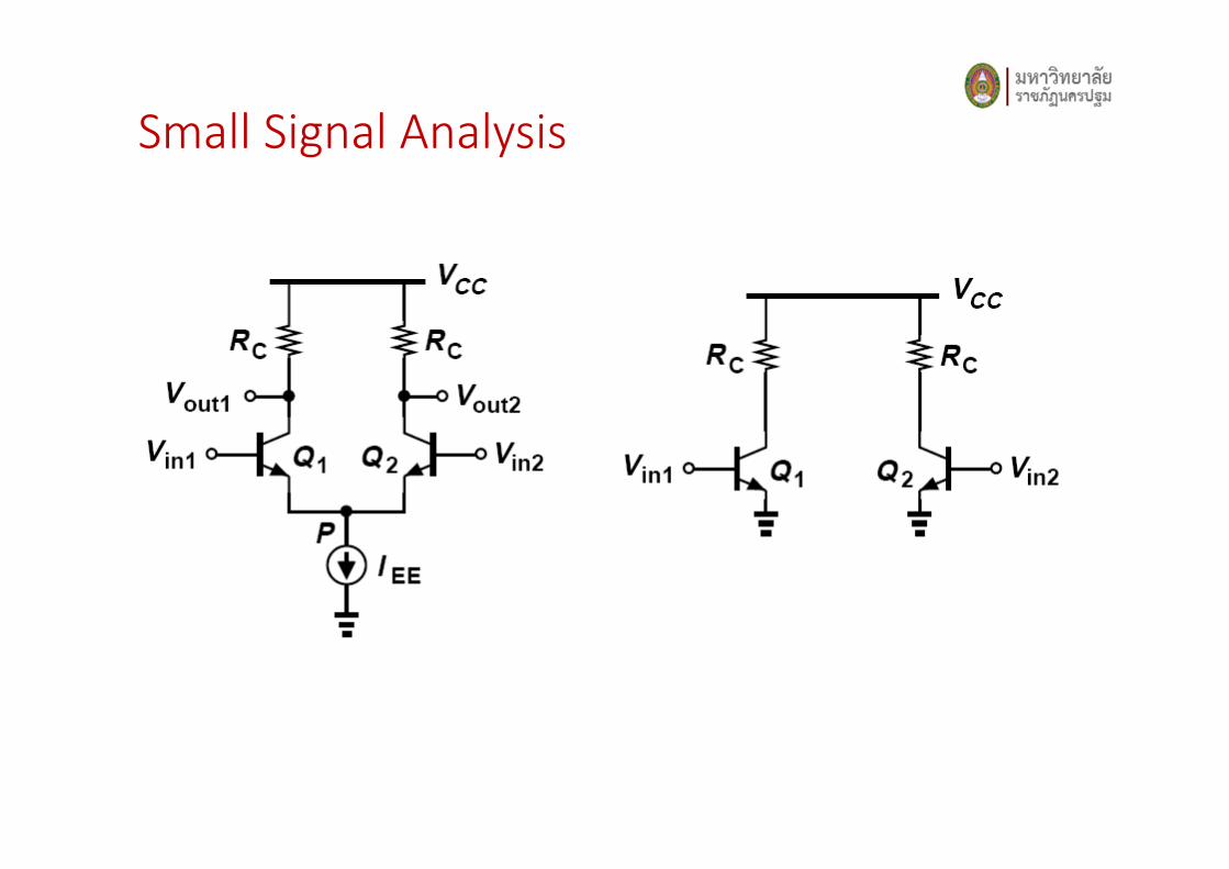
Small Signal Analysis

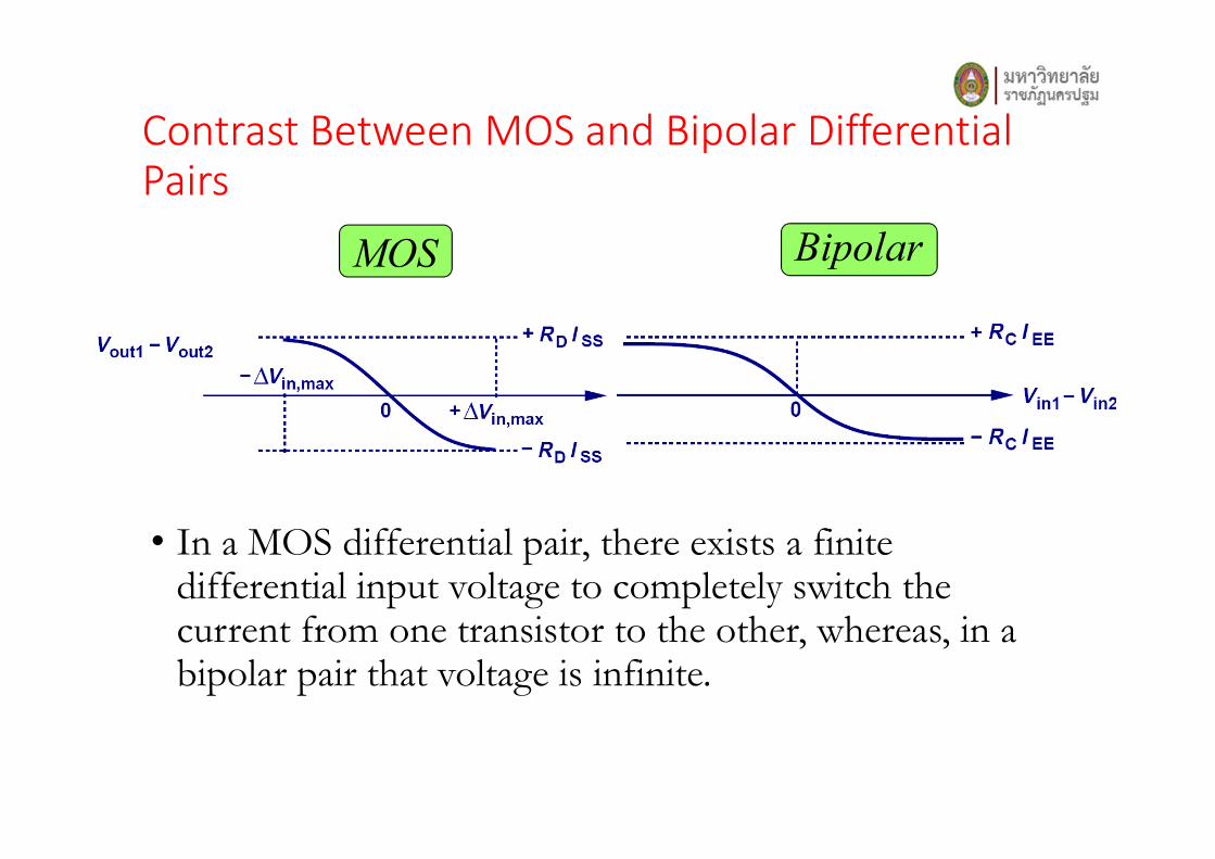
Contrast Between MOS and Bipolar Differential Pairs
• In a MOS differential pair, there exists a finite differential input voltage to completely switch the current from one transistor to the other, whereas, in a bipolar pair that voltage is infinite.
MOS Bipolar
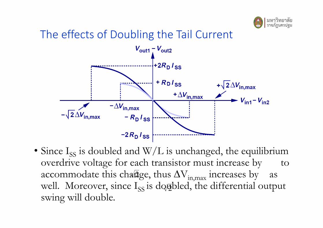
The effects of Doubling the Tail Current
• Since ISS is doubled and W/L is unchanged, the equilibrium overdrive voltage for each transistor must increase by to accommodate this change, thus ∆Vin,max increases by as well. Moreover, since ISS is doubled, the differential output swing will double.
2
2
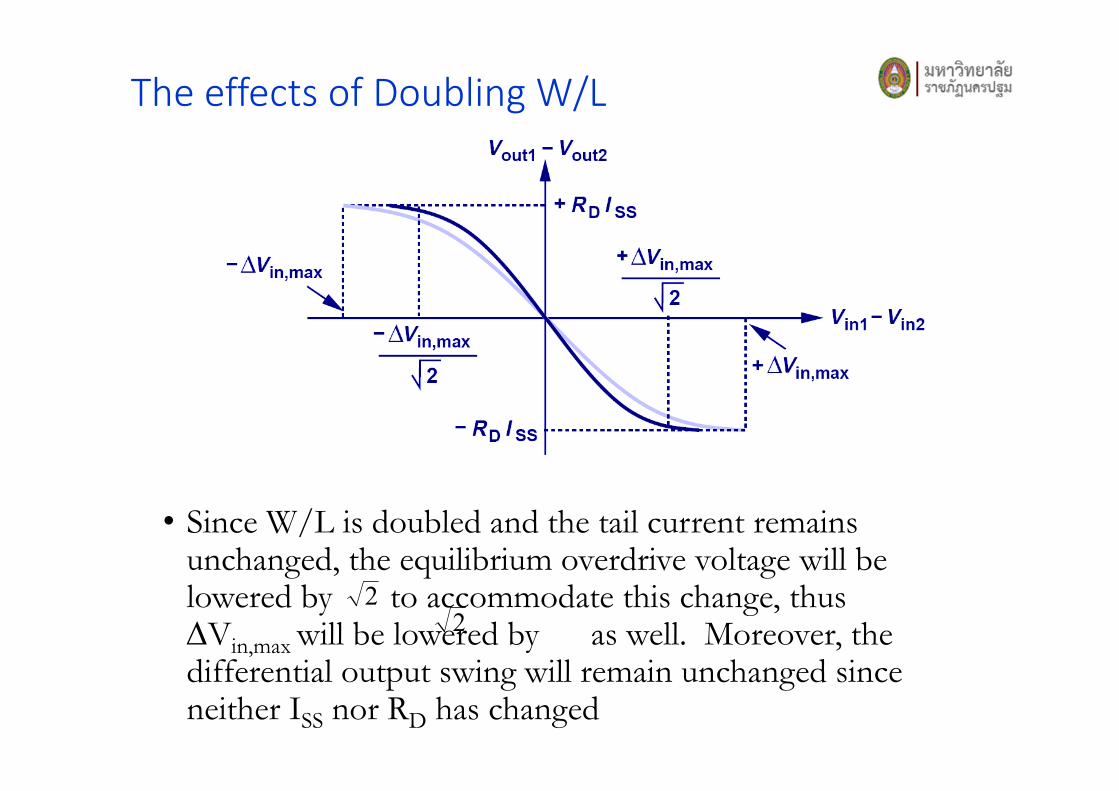
The effects of Doubling W/L
• Since W/L is doubled and the tail current remains unchanged, the equilibrium overdrive voltage will be lowered by to accommodate this change, thus ∆Vin,max will be lowered by as well. Moreover, the differential output swing will remain unchanged since neither ISS nor RD has changed
2
2
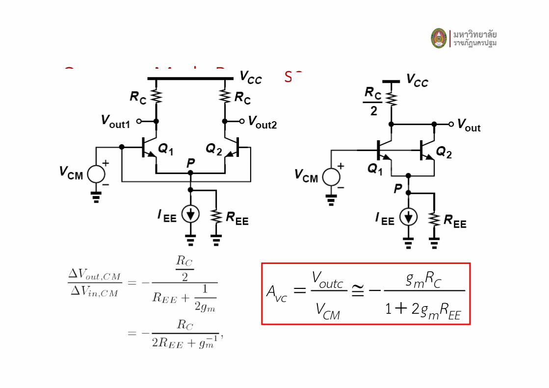
Common Mode Response
1 2outc m C
vcCM m EE
V g RA
V g R= ≅ −
+
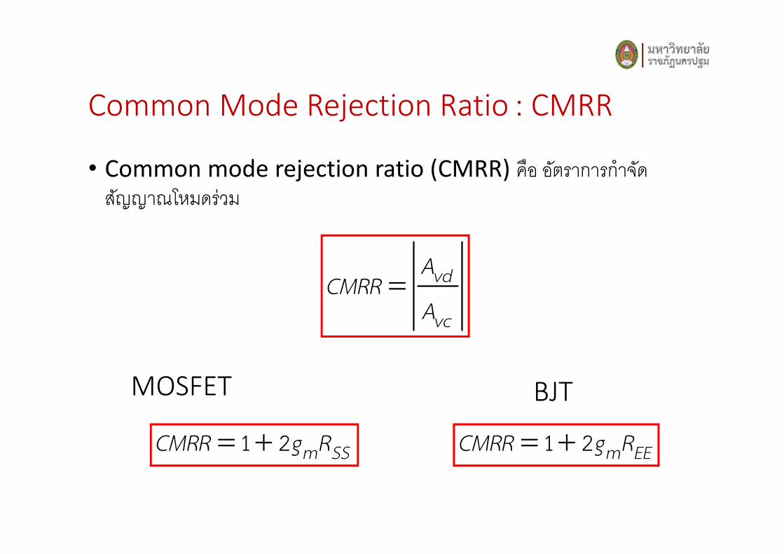
Common Mode Rejection Ratio : CMRR
• Common mode rejection ratio (CMRR) คือ อตัราการกําจดั
สญัญาณโหมดร่วม
vd
vc
ACMRR
A=
1 2 m SSCMRR g R= +
MOSFET BJT
1 2 m EECMRR g R= +

Ex 7.1 VDD=VSS=1.5 V, RD
= 2.5 k and M1= M2 has KN
= 2 mA/V2
VTH
= 0.5 V and ISS
= 0.4 mA Find Vout

Ex 7.2 VDD
=VSS
=1.5 V, RD
= 2.5 k and M1= M2 has KN
= 2 mA/V2
VTH
= 0.5 V and ISS
= 0.4 mA Find Vout
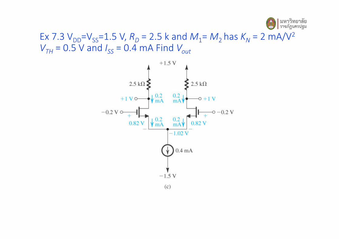
Ex 7.3 VDD=VSS=1.5 V, RD
= 2.5 k and M1= M2 has KN
= 2 mA/V2
VTH
= 0.5 V and ISS
= 0.4 mA Find Vout

Offset Voltage to compensate
Figure 7.25 (a) The MOS differential pair with both inputs grounded.
Owing to device and resistor mismatches, a finite dc output voltage VO
results. (b) Application of a voltage equal to the input offset voltage
VOS
to the terminals with opposite polarity reduces VO
to zero.
• สาเหตุที�เกิดแรงดนัออฟเซตคือค่าความตา้นทานของโหลด และค่า KN
และ VTH
ของมอสที�เป็นคู่ผลต่างไม่เท่ากนั
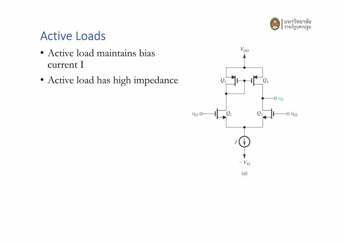
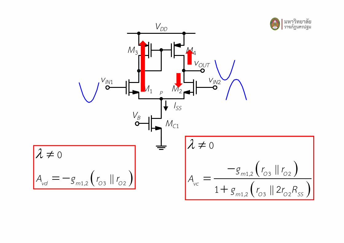
Active Loads
• Active load maintains bias current I
• Active load has high impedance
VDD
M1 M2
MC1
P
ISS
vIN2vIN1
M3 M4vOUT
VB
VDD
M1 M2
MC1
P
ISS
vIN2vIN1
M3 M4vOUT
VB
( )1,2 3 2
0
||vd m O OA g r r
λ ≠
= −( )( )1,2 3 2
1,2 3 2
0
||
1 || 2
m O O
vc
m O O SS
g r rA
g r r R
λ ≠
−=
+
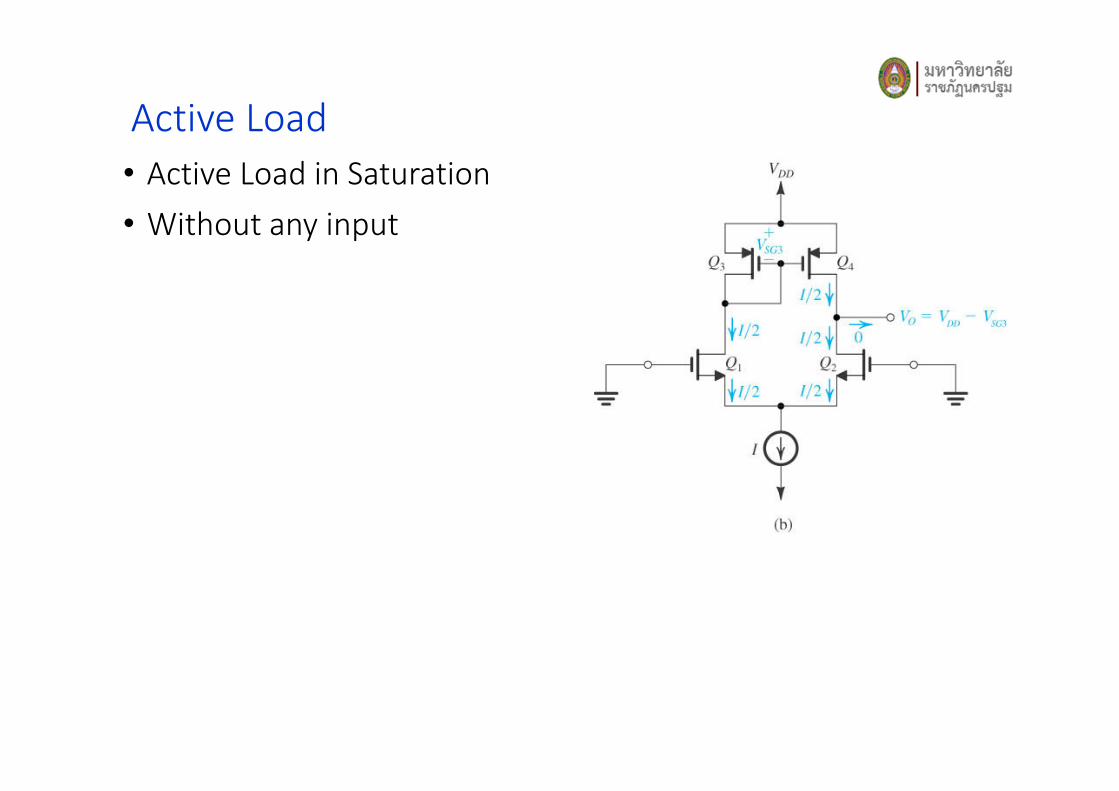
Active Load
• Active Load in Saturation
• Without any input
Active Load
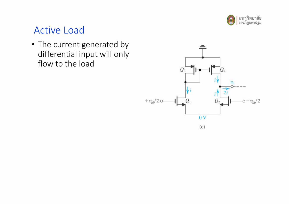
• The current generated by differential input will only flow to the load
Active Load
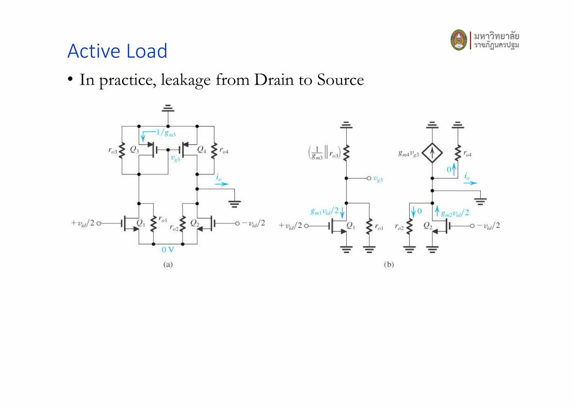
• In practice, leakage from Drain to Source

Reference
1. Adel S. Sedra, Kenneth C. Smith “Microelectronic Circuit”
2. Pual R. Gray and Robert G. Mayer “Analysis and Design of Integrated Circuit”