Embed Size (px)
Citation preview

Direct Detection Optical OFDM (DD-OOFDM):Theory and First Experiments
Abdulamir Ali, Jochen Leibrich, Werner Rosenkranz(aal@tf uni-kiel de)([email protected])
Christian-Albrechts-Universität zu Kiel
Berlin, 7. July 2009
L N T

Motivation
• In DD-OOFDM, modulator bias was shown by simulation to
be a key parameter to achieve high sensitivity– be a key parameter to achieve high sensitivity
– allow for balancing spectral efficiency versus sensitivity
• Aim of this contribution:
– to show the improvement of sensitivity due to optimized biasing by a
theoretical model
– to experimentally verify the impact of modulator bias on sensitivity
– to show several experiments aiming at optimization of sensitivity
-2-L N T
Chairfor Communications
Lehrstuhl fürNachrichten- und Übertragungstechnik
J. Leibrich and A. Ali, Workshop on Optical Communications, July 2009 , Berlin

Outline
1. Introduction
2. Theoretical model for impact of MZM biasing
3. Experimental results
first experiments (proof of concept)– first experiments (proof of concept)
– experiments aiming at improved sensitivity
4. Conclusion
-3-L N T
Chairfor Communications
Lehrstuhl fürNachrichten- und Übertragungstechnik
J. Leibrich and A. Ali, Workshop on Optical Communications, July 2009 , Berlin

Introduction: OOFDM Principles
• Direct detection optical-OFDM Simple (low effort)
Needs carrier (low sensitivity) and frequency gap (spectrally inefficient )Needs carrier (low sensitivity) and frequency gap (spectrally inefficient )Laser
OFDM
• Coherent detection optical-OFDM
MZMOpticalchannel
De-mod
OFDMmod.
Coherent detection optical-OFDM High sensitivity (no carrier) and high spectral efficiency (no gap)
Complex receiver
OpticalOFDMMod
MZM
Re
Im
OFDMDe-
Re900H
y
LO1
Opticalchannel
Mod.
MZM 900
Im
mod.
Im
brid
LO2
-4-L N T
Chairfor Communications
Lehrstuhl fürNachrichten- und Übertragungstechnik
J. Leibrich and A. Ali, Workshop on Optical Communications, July 2009 , Berlin
LO2

Introduction: Modulator (MZM) bias
• Transfer characteristic of MZM
Pout, Eout
+1r
Optical
power
eld
and
pow
er
Bias at quadrature
Bias at
1 0 8 0 5 0 1vmod/V
E-field
-1
Rel
ativ
e fi Bias at
|Vbias/V|=0.8
• Bias point strong carrier power l li i t
-1 -0.8 -0.5 0 1
sign
al
Electrical reduced carrier power li i t low nonlinear impact
|Vbias/V|=0.5 (quadrature point)
Driv
ing
s
|Vbias/V|=0.8 more nonlinear impact
-5-L N T
Chairfor Communications
Lehrstuhl fürNachrichten- und Übertragungstechnik
J. Leibrich and A. Ali, Workshop on Optical Communications, July 2009 , Berlin

Theoretical Model: Setup for Receiver
• Optically preamplified receiver
( )( )EDFA
Bo Be
E ta( ) i tp( ) i t( )E tp( )
• Back-to-back transmission: receiver input signal Ea(t) is equal to MZM output signal
• Modeling in bandpass domain:
cos 2 cos 2biasMZM a c
s t VE t E t P f t
2MZM a cfV with:
s(t) : OFDM-signal driving the MZMV : bias voltage of MZMVbias : bias voltage of MZMV : switching voltage of MZMP : optical output power of CW-laserf : optical carrier frequency
-6-L N T
Chairfor Communications
Lehrstuhl fürNachrichten- und Übertragungstechnik
J. Leibrich and A. Ali, Workshop on Optical Communications, July 2009 , Berlin
fc : optical carrier frequency

Theoretical Model: Computation
• After EDFA and optical filter:
2 2biass t VE P fG
cos 2 co
cos 2 sin
s 22
2i c q c
biasp cE t
n t f t n t f
P f tV
t
G
i c q cf f
with:ni(t), nq(t) : in-phase and quadrature component of EDFA noise
• After photodiode with responsivity R:
G : EDFA gain
After photodiode with responsivity R:
2cos2
biasp
s t Vi t R GP
V
2 22 co
2
.2
1s2
biasi i qn t
s t Vn t GP n
Vt
V
-7-L N T
Chairfor Communications
Lehrstuhl fürNachrichten- und Übertragungstechnik
J. Leibrich and A. Ali, Workshop on Optical Communications, July 2009 , Berlin
2 2V

Theoretical Model: Expression for BER
• First-order approximation results in electrical signal-to-noise ratio:22 'S B V 2tan
2 2o s bias
e
S B VOSNRN B V V
with:OSNR : optical signal-to-noise ratio
• In case of QPSK-modulation:
Bo’ : optical reference bandwidth
s : standard deviation of OFDM-signal
In case of QPSK modulation:
22 '21 1 1 1erfc erfc tano s biasS B VBER OSNR 2erfc erfc tan
2 2 2 2 2 2o s bias
e
BER OSNRN B V V
-8-L N T
Chairfor Communications
Lehrstuhl fürNachrichten- und Übertragungstechnik
J. Leibrich and A. Ali, Workshop on Optical Communications, July 2009 , Berlin

Theoretical Model: Results
• 10Gb/s DD-OOFDM b2b with QPSKsubcarrier modulationOSNR(0 1 ) f BER 10 3
22 '21 1erfc tano s biasB VBER OSNR • OSNR(0.1nm) req. for BER=10-3 vs.
modulator biaserfc tan
2 2 2 2e
BER OSNRB V V
15 GHz
• Solid line: theoretical model– neglects nonlinearity of
50
45
4010-3 s=0.01V– neglects nonlinearity of
• modulator• photo diode
40
35
30
B]@
BER=
1
s=0.05V
0 1• Dashed line: numerical results– include nonlinearity– best sensitivity ≈13dB OSNR
25
20O
SNR
[dB s=0.1V
s=0.2V
– best sensitivity ≈13dB OSNR 15
10-1 -0.9 -0.8 -0.7 -0.6 -0.5
V Vbias/
-9-L N T
Chairfor Communications
Lehrstuhl fürNachrichten- und Übertragungstechnik
J. Leibrich and A. Ali, Workshop on Optical Communications, July 2009 , Berlin
bias

Outline
1. Introduction
2. Theoretical model for impact of MZM biasing
3. Experimental results
first experiments (proof of concept)– first experiments (proof of concept)
– experiments aiming at improved sensitivity
4. Conclusion
-10-L N T
Chairfor Communications
Lehrstuhl fürNachrichten- und Übertragungstechnik
J. Leibrich and A. Ali, Workshop on Optical Communications, July 2009 , Berlin
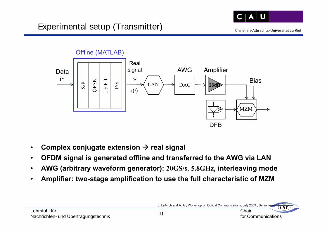
Experimental setup (Transmitter)
Offline (MATLAB)
Real
S/P
QPS
K
F F
T
P/S
Datain
DAC
Realsignal
(t)
AWG Amplifier
26dBBiasLAN
Q I F s(t)
MZM
DFB
• Complex conjugate extension real signal• OFDM signal is generated offline and transferred to the AWG via LAN• AWG (arbitrary waveform generator): 20GS/s 5 8GHz interleaving mode• AWG (arbitrary waveform generator): 20GS/s, 5.8GHz, interleaving mode• Amplifier: two-stage amplification to use the full characteristic of MZM
-11-L N T
Chairfor Communications
Lehrstuhl fürNachrichten- und Übertragungstechnik
J. Leibrich and A. Ali, Workshop on Optical Communications, July 2009 , Berlin

Experimental setup (Receiver)
ADC LANOpticalAtt 2
OpticalAtt 1
EDFA ScopeBe=12GHzReceivedopticalsignal Att.2Att.1signal
S/P
F F
T
QPS
K-1
P/SSynch.2.5 BER
Offline (MATLAB)
F Q
Referencesignal
• Optical Att.1: OSNR tuning• Optical Att.2: controls input power to photodoide
S ( l ti li ill ) 50GS/ BW 18GH
Offline (MATLAB)
• Scope (real-time sampling oscilloscope): 50GS/s, BW=18GHz• Synchronization: first 4 OFDM symbols (reference signal) to find maximum
correlation (start of time signal)
-12-L N T
Chairfor Communications
Lehrstuhl fürNachrichten- und Übertragungstechnik
J. Leibrich and A. Ali, Workshop on Optical Communications, July 2009 , Berlin

System parameters
• Back-to-back transmission• QPSK modulation• 1024 OFDM symbols• NFFT=2048 • Data ratesData rates
10Gb/s: N=511, no frequency gap Wg=0 5 Gb/s : N=256, with frequency gap Wg=N
10Gb/s 5Gb/s
5 GHz 2.5 GHzAWG output AWG output
-13-L N T
Chairfor Communications
Lehrstuhl fürNachrichten- und Übertragungstechnik
J. Leibrich and A. Ali, Workshop on Optical Communications, July 2009 , Berlin

Experimental results
• DSB transmission• Direct output from AWG
Synchronization Received constellation1
0.5
Rx signal after synch.Tx. signal
0
Am
plitu
de
-0.5
due to noise from AWG
2750 2800 2850 2900 2950 3000-1
Sample
-14-L N T
Chairfor Communications
Lehrstuhl fürNachrichten- und Übertragungstechnik
J. Leibrich and A. Ali, Workshop on Optical Communications, July 2009 , Berlin

Experimental results
10Gb/s: comparison between theoretical and measurement results
• DSB transmission
• Vbi =0.5V (quad. point), σ =0.05V
1
theoreticalmeasurement
----Vbias 0.5V (quad. point), σs 0.05V
deviation from theoretical because f i t f IMD d th l i
2
BER
) 2.8dB
of impacts of IMD and thermal noise
BER floor @ BER≈10-5
3
4
-log 10
(B
3.4dB
5.1dB@
20 22 24 26 28 30 32 34 36 38
4
5
6
OSNR[dB]
-15-L N T
Chairfor Communications
Lehrstuhl fürNachrichten- und Übertragungstechnik
J. Leibrich and A. Ali, Workshop on Optical Communications, July 2009 , Berlin

Experimental results
10Gb/s: influence of modulation depth σs
• DSB transmission
• Vbi =0.5V (quad. point)
1
0 05s/VVbias 0.5V (quad. point)
Measured improvement is less thanth ti l i t
2
BER
) 4.1dB
0.050.10.150.2
theoretical improvement
BER floor for small and large 3
4
-log 10
(B
signals
BER floor for σs=0.2V starts earlier b f hi h MZM li it 20 22 24 26 28 30 32 34 36 38
4
5
6
because of high MZM nonlinearity OSNR[dB]
-16-L N T
Chairfor Communications
Lehrstuhl fürNachrichten- und Übertragungstechnik
J. Leibrich and A. Ali, Workshop on Optical Communications, July 2009 , Berlin

Experimental results
5Gb/s: benefit of frequency gap
• DSB transmission
• Vbi =0.5V (quad. point), σ =0.05V
1
without gapwith gapVbias 0.5V (quad. point), σs 0.05V
Improvement of ~6.5dB @ BER=10-3 2
BER
)
3dB for half data rate 3.5dB benefit of the gap 3
4
-log 10
(B
~ 6.5dB
With gap no BER floor
20 22 24 26 28 30 32 34 36 38
4
5
6
OSNR[dB]
-17-L N T
Chairfor Communications
Lehrstuhl fürNachrichten- und Übertragungstechnik
J. Leibrich and A. Ali, Workshop on Optical Communications, July 2009 , Berlin

Experimental results
5Gb/s: influence of modulation depth σs
• DSB transmission
• Vbi =0.5V (quad. point)
1
s/VVbias 0.5V (quad. point)
Modulation depth should be b t 0 1V d 0 2V
2
BER
)
0.050.10.150.2
between 0.1V and 0.2V
σs= 0.2V, MZM nonlinearity is high 3
4
-log 10
(B
s y g BER floor at BER≈10-5
15 17 19 21 23 25 27 29 30
4
5
6
OSNR[dB]
-18-L N T
Chairfor Communications
Lehrstuhl fürNachrichten- und Übertragungstechnik
J. Leibrich and A. Ali, Workshop on Optical Communications, July 2009 , Berlin

Experimental results
1
V /V
5Gb/s: influence of bias point for σs=0.2V
• DSB transmission0.50.60.70 8
Vbias/V
20(B
ER)
0.80.9
3-log 10
4
5
6
• Asymmetrical clipping performs better than symmetrical clipping
15 17 19 21 23 25 27 29 306
OSNR[dB]
-19-L N T
Chairfor Communications
Lehrstuhl fürNachrichten- und Übertragungstechnik
J. Leibrich and A. Ali, Workshop on Optical Communications, July 2009 , Berlin
Asymmetrical clipping performs better than symmetrical clipping

Discussion
• Stability: A DC voltage applied to the bias port may induce drift in the operating
point over time adjustment is requiredp j q
• improvement:O ti l filt ft EDFA f ASE i d tiOptical filter after EDFA for ASE noise reductionElectrical filter after PD for thermal noise reduction
• SSB transmission (with optical channel)Avoid power fading due to chromatic dispersion
-20-L N T
Chairfor Communications
Lehrstuhl fürNachrichten- und Übertragungstechnik
J. Leibrich and A. Ali, Workshop on Optical Communications, July 2009 , Berlin

SSB transmission
OFDMsignal Bias
EDFA FBGDAC EDFA
AWG
MZM SSBfilter
EDFA(booster)
ASEfilter
FBG0.2nmtunable
DACBe=12GHz
ADC DSP
EDFA(preamp.) Scope
Transfer function:3dB BW≈0 4nm -20dB transition BW≈10GHzTransfer function:3dB BW≈0.4nm 20dB transition BW≈10GHz
20dBm 23dBm
0.4nm( 50GH ) 0.085nm
(~10GHz)(~50GHz)
-21-L N T
Chairfor Communications
Lehrstuhl fürNachrichten- und Übertragungstechnik
J. Leibrich and A. Ali, Workshop on Optical Communications, July 2009 , Berlin

SSB Transmission
• Optimization: trade off between sideband suppression and bias point Low sideband suppression: biasing near null power point High sideband suppression: biasing near quadrature point
SSB filter
f [GHz]-5 -2.5 0 2.5 5
2
2.5
3og10
(BER
)
3
3.5
4
-Lo
-22-L N T
Chairfor Communications
Lehrstuhl fürNachrichten- und Übertragungstechnik
J. Leibrich and A. Ali, Workshop on Optical Communications, July 2009 , Berlin
0.75 0.8 0.85 0.9 0.954
Vbias/V

Experimental results
1
5Gb/s: B2B transmission
DSBSSB
2
0(BER
)
3
4
-Log
1
~2dB
4
565 6 7 8 9 10 11 12 13 14 15
6
OSNR[dB]
-23-L N T
Chairfor Communications
Lehrstuhl fürNachrichten- und Übertragungstechnik
J. Leibrich and A. Ali, Workshop on Optical Communications, July 2009 , Berlin

Experimental results
• SSB transmission• Received at OSNR=10dB and BER ~ 1e-3
Time signal and spectrum after photodiode Constellation
Time signal
spectrum
Intermodulation distortion
-24-L N T
Chairfor Communications
Lehrstuhl fürNachrichten- und Übertragungstechnik
J. Leibrich and A. Ali, Workshop on Optical Communications, July 2009 , Berlin

Conclusions
• Analytical:The increase in sensitivity when optimizing MZM bias voltage is treated
analytically for DD-OOFDManalytically for DD-OOFDMGood agreement of theoretical analysis and numerical simulation over a wide
range of values for the bias voltage
• Experimental: sources of sensitivity degradationMZM nonlinearity driving signal of appropriate amplitude σs=0.1V
….0.2V
Ph di dPhotodiode • Intermodulation distortion IMD needs frequency gap• Thermal noise needs filter
• Further aspects (with optical channel) Synchronization: training symbol Synchronization: training symbol Channel estimation: number of OFDM symbol required
-25-L N T
Chairfor Communications
Lehrstuhl fürNachrichten- und Übertragungstechnik
J. Leibrich and A. Ali, Workshop on Optical Communications, July 2009 , Berlin

Thank youThank you
-26-L N T
Chairfor Communications
Lehrstuhl fürNachrichten- und Übertragungstechnik
J. Leibrich and A. Ali, Workshop on Optical Communications, July 2009 , Berlin

-27-L N T
Chairfor Communications
Lehrstuhl fürNachrichten- und Übertragungstechnik
J. Leibrich and A. Ali, Workshop on Optical Communications, July 2009 , Berlin

![Single Molecule Microscopy and Hole-Burning Spectroscopy ...€¦ · droplets [xvi,xvii] using confocal microscopes and sensitive optical detection schemes. Direct imaging of single](https://img.pdfslide.tips/doc/110x75/5ed9264f6714ca7f47693d21/single-molecule-microscopy-and-hole-burning-spectroscopy-droplets-xvixvii.jpg)