Embed Size (px)
Citation preview
Silicon Wafer Related Productsシリコンウエハー搬送資材・関連商品
Improved protection & transportation system for valuable Semiconductor
されたウエハーパッケージシステムは、お客様のウエハーを安全且つ効率的に搬送致します。 TSV用薄膜ウエハーや化合物ウエハー等、割れ易いウエハーの搬送でお困りの際もぜひアキレスにご相談ください。
Achilles Wafer Package System, developed making good use of Achilles’ plastics processing technologies (injection forming, film processing, foam processing, conductive processing, etc.), can transfer/transport your wafers both safely and efficiently. Whenever you have trou-bles with transferring/transporting such highly fragile wafers as thin wafer for TSV chips and compound wafers, please contact us. We are ready to provide you with optimum solutions.
Materials & Products

・ コンパクトデザインにより輸送コストを削減できます。・ 密閉性に優れています。・ 各ウエハーサイズに対応しています。・ 自動ウエハー移載装置に対応しています。
MA-12/ONE-SP (with separate-type blue clips) MA-12/ONE-FX (with fixed-type black clips)
・ 12inchウエハーを1枚で搬送可能です。・ クリーン導電材(STポリ)を使用しています。・ 重ねて保管・輸送が可能です。・ 試作用ウエハー搬送に最適です。
<1.0×10⁶Ω
conductive PP
Wafer Case Conductive PC Blue clip PCBlack clip PP
separate-type blue clips fixed-type black clips
VFS-4-6R-65(for 4inch Compound Wafer) VFS-6-8R-65(for 6inch Compound Wafer)
・ 割れ易い化合物ウエハーの搬送が可能です。・ 化合物ウエハーの非接触搬送が可能です。・ 低パーティクル・ 低アウトガス・ 高透明性
<1.0×10⁷Ω
conductive A-PET
Protos Carrier MA Series /プロトスキャリアMAシリーズMA-4/5/6S/8/8S/12
Product name
Product No.
Material
Features
特 長
Resistance
Dimensions
・ Compact design to save transportation cost.・ Good airtight container.・ Industry standard wafer sizes available.・ Feasible design for automated handling machine.
Protos inner tray /プロトスインナートレーProduct name
Product No.
Material
Features
特 長
Resistance
<1.0×10⁷Ω
Product No.
Material
Features
特 長
Resistance
Wafer
Wafer Package System / ウエハー用
Wafer Package System for Single / 12inchウエハー1枚入り用
Wafer Package System for Compounding Wafer / インナートレー(化合物ウエハー用)
Protos Cushion
Protos CarrierTOP
Protos CarrierTOP
Protos CarrierTOP
Wafer
Wafer
Protos CarrierBTM
Protos CarrierBTM
Protos CarrierBTM
Protos Spacer
Protos Spacer
Protos Spacer
Inner Tray×2pcs
×12set
Protos Spacer
Protos Cushion
Protos Cushion
Protos Cushion
Protos Cushion
Protos Cushion×2pcs
Protos Spencer×2pcs
Wafer×1pcs
Protos Spencer×1pcs
Inner Tray×1pcs
Protos Cushion
Protos Spacer
How to Packing
ProductNo.
「H」Containerheight (mm)
「h」Effectiveheight (mm)
「D」Effectivediameter (mm)
「A」Containerdiameter (mm)
MA-4
MA-5
MA-6S
MA-8
MA-8S
MA-12
90
90
63
103
65
76
47.8
50
38
54
38
44
103±1
128±1
153±1
203±1
203±1
302±1
150
150
175
226
226
328
・ Single piece of 12-inch wafer can be transferred/transported.・ Using clean conductive material(ST Poly)・ Can be stacked during storage/transportation.・ Optimum for transporting test production wafers
・ Can transfer/transport brittle compounding wafers.・ Adopting clean conductive material(ST-poly)・ Low particle level・ Low outgas generation・ High transparency
※MA-12→SEMI standard/SEMI G90
1
ND-6
ND-8
ND-12
83
92
74
40
57
45
230±1
299±1
403±1
252
322
430
・ コンパクトデザインにより輸送コストを削減できます。・ ダイシングウエハーをフレーム付きで収納できます。・ プロトスフレームと併用で軽量搬送が可能になります。
ND-12
ND-6/8
Product No. RemarksO.D.(mm)
I.D.(mm)
Thickness(mm)
Weight(g)
150LF-FF-AR
200LF-FF-AR
200LF-EP-AR
300LF-EP-AR
228
296
296
400
194
250
250
350
1.5
1.5
2.0
2.5
28
45
60
120
Full flat
Full flat
Label-capable
Label-capable
VFP-6R-90FG(フレーム+グリップリング)VFP-ND-8R-90(フレーム付8inch用)VFP-ND-12R-90(フレーム付12inch用)
・ フレーム付きウエハーを1枚で搬送可能です。・ フレーム部で固定するためウエハーは非接触です。・ クリーン導電材(STポリ)を使用しています。・ 試作用ウエハー搬送に最適です。
<1.0×10⁷Ω
conductive A-PET
Protos Carrier ND Series /プロトスキャリア NDシリーズND-6/8/12(Figures are wafer dia. in inch)(数字はウエハーサイズ inch)
(ND-6/8)Conductive PP(ND-12)Antistatic PC/ABS
ND-6,8:<1.0x10⁶ΩND-12 :<1.0x10¹²Ω
Product name
Product No.
Protos Frame / プロトスフレーム
150/200/300LF-EP/FF-AR(Figures are wafer dia. in inch)(数字はウエハーサイズ inch)
Product name
Product No.
Material
Features
特 長
Resistance
Dimensions
・ 樹脂性フレームのため軽量化が可能になります。(メタルフレームより重量比約50%削減)・ SEMI規格準拠(300mm用) ※他サイズ、ESD対応も可能です。
特 長
Dimensions
・ Compact design can reduce transportation costs.・ Can store dicing wafers together with frames attached to the wafers.・ Use in combination with Protos Frames enables light weight transfer/transportation.
Features・ Plastic frames allow reduction in transportation weight. (Frame weight can be reduced by 50% when compared with metal frame.)・ Made in accordance with SEMI standards(for 300mm)
Product No.
特 長
Features
Material
Resistance
・ Single piece of wafer with frame can be transferred/ transported.・ As frame is used for fixing, there is no contact with wafer.・ Using clean conductive material(ST Poly)・ Optimum for transporting test production wafers
※For Protos Frames of other sizes than the above and those for ESD applications, we are ready to respond to your requirements. So please contact us.※他サイズ、ESD対応も要相談
※SEMI standard/SEMI G87
※ND-12→SEMI standard/SEMI G94、G87
Tape Frame
Wafer Package System for Film Frame / フィルムフレーム用
Wafer Package System for Single Film Frame / フィルムフレーム用
Protos CarrierTOP
Protos CarrierBTM
Film Frame CarrierBTM
Film Frame CarrierTOP
Protos Cushion
Wafer
Wafer
Protos Frame + Wafer
Protos Spacer
Protos Spacer
Protos Spacer
Protos Cushion
Protos Spacer
How to Packing
ProductNo.
「H」Containerheight (mm)
「h」Effectiveheight (mm)
「D」Effectivediameter (mm)
「A」Containerdiameter (mm)
2
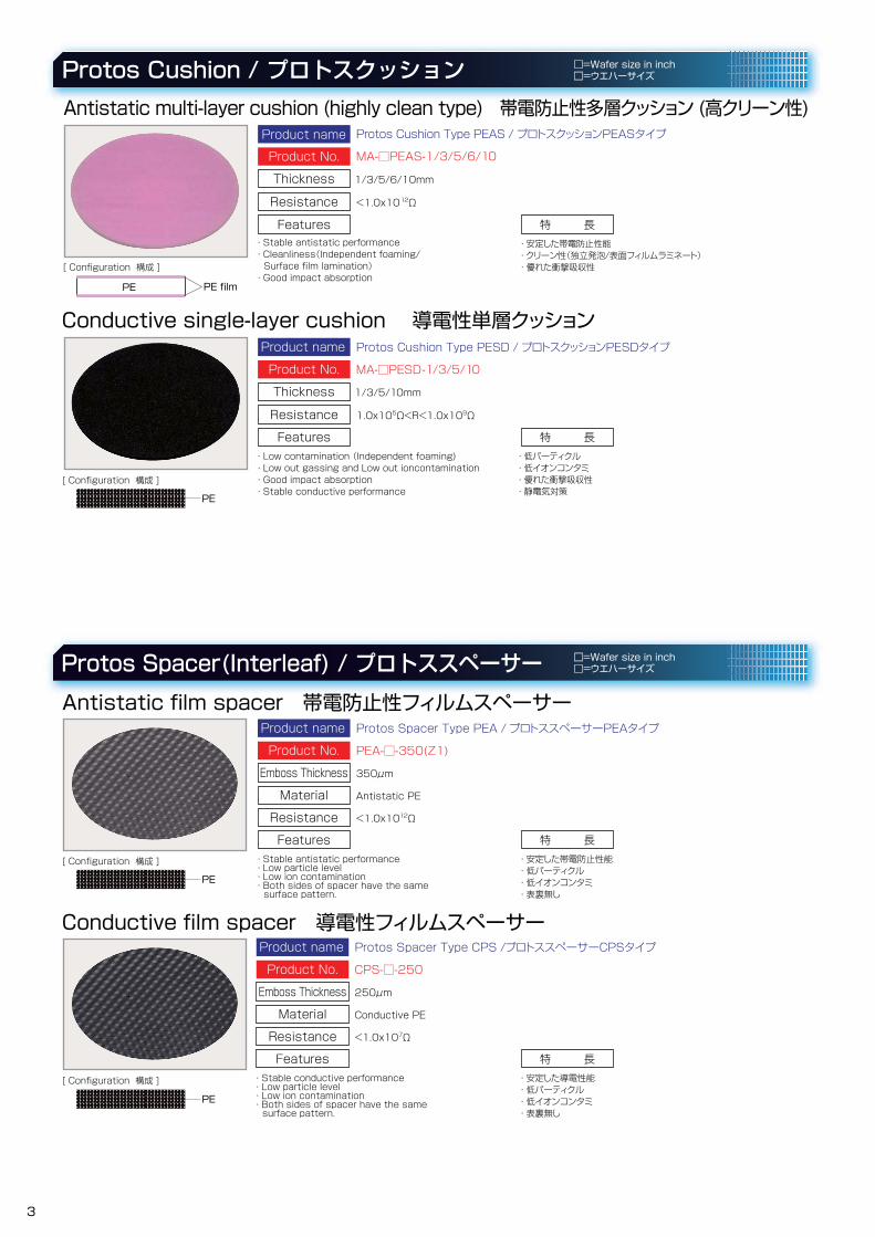
Protos Cushion / プロトスクッション
Protos Spacer(Interleaf) / プロトススペーサー
□=Wafer size in inch□=ウエハーサイズ
□=Wafer size in inch□=ウエハーサイズ
Protos Cushion Type PEAS / プロトスクッションPEASタイプ
MA-□PEAS-1/3/5/6/10
1/3/5/6/10mm
Product name
Product No.
Thickness
<1.0x10¹²Ω
・ Stable antistatic performance・ Cleanliness(Independent foaming/ Surface film lamination)・ Good impact absorption
Resistance
Features・ 安定した帯電防止性能・ クリーン性(独立発泡/表面フィルムラミネート)・ 優れた衝撃吸収性
Antistatic multi-layer cushion (highly clean type) 帯電防止性多層クッション (高クリーン性)
[ Configuration 構成 ]
PE PE film
Protos Cushion Type PESD / プロトスクッションPESDタイプ
MA-□PESD-1/3/5/10
1/3/5/10mm
Product name
Product No.
Thickness
1.0x10⁵Ω<R<1.0x10⁹Ω
・ Low contamination (Independent foaming)・ Low out gassing and Low out ioncontamination・ Good impact absorption・ Stable conductive performance
Resistance
Features・ 低パーティクル・ 低イオンコンタミ・ 優れた衝撃吸収性・ 静電気対策
Conductive single-layer cushion 導電性単層クッション
[ Configuration 構成 ]
PE
[ Configuration 構成 ]
PE
[ Configuration 構成 ]
PE
Antistatic film spacer 帯電防止性フィルムスペーサー Protos Spacer Type PEA / プロトススペーサーPEAタイプ
PEA-□-350(Z1)
350μm
Antistatic PE
<1.0x10¹²Ω
・ Stable antistatic performance・ Low particle level・ Low ion contamination・ Both sides of spacer have the same surface pattern.
Product name
Product No.
Emboss Thickness
Material
Resistance
Features・ 安定した帯電防止性能・ 低パーティクル・ 低イオンコンタミ・ 表裏無し
Protos Spacer Type CPS /プロトススペーサーCPSタイプ
CPS-□-250
250μm
Conductive PE
<1.0x10⁷Ω
・ Stable conductive performance・ Low particle level・ Low ion contamination・ Both sides of spacer have the same surface pattern.
Product name
Product No.
Emboss Thickness
Material
Resistance
Features・ 安定した導電性能・ 低パーティクル・ 低イオンコンタミ・ 表裏無し
Conductive film spacer 導電性フィルムスペーサー
特 長
特 長
特 長
特 長
3
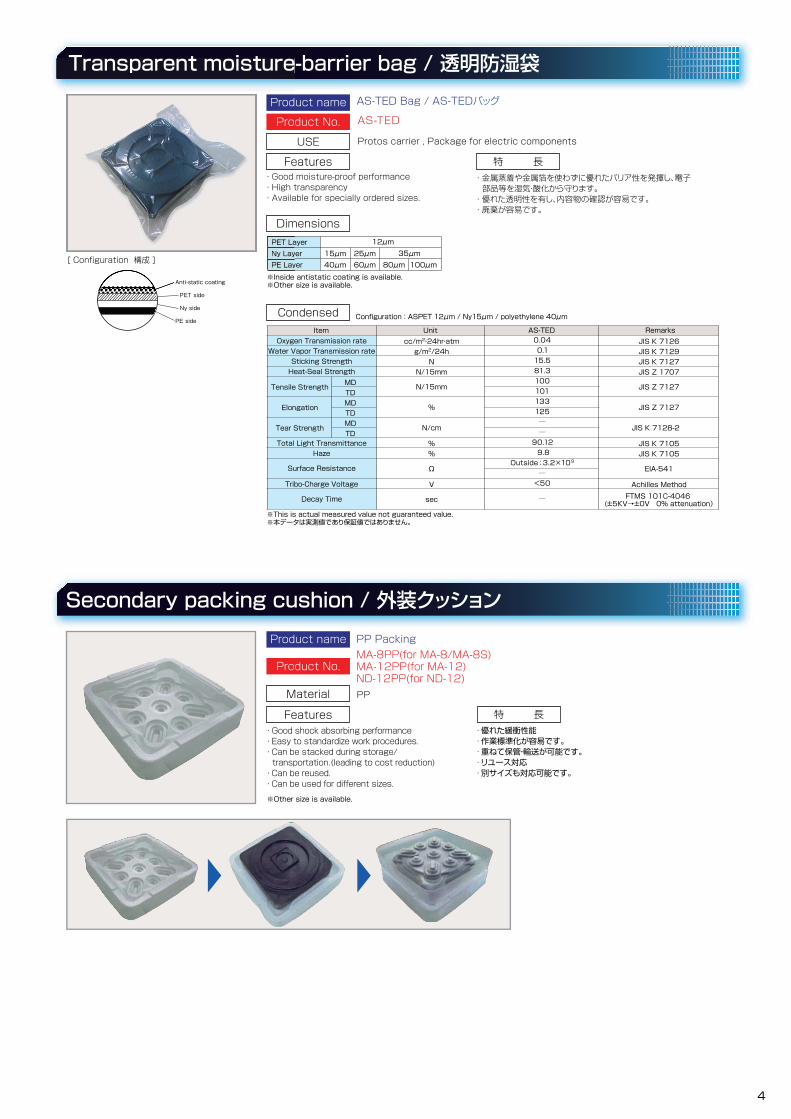
Transparent moisture-barrier bag / 透明防湿袋
Secondary packing cushion / 外装クッション
・ 優れた緩衝性能・ 作業標準化が容易です。・ 重ねて保管・輸送が可能です。・ リユース対応・ 別サイズも対応可能です。
PP Packing
PP
MA-8PP(for MA-8/MA-8S)MA-12PP(for MA-12)ND-12PP(for ND-12)
・ Good shock absorbing performance・ Easy to standardize work procedures.・ Can be stacked during storage/ transportation. (leading to cost reduction)・ Can be reused.・ Can be used for different sizes.
PET LayerNy LayerPE Layer
15μm40μm
25μm60μm 80μm 100μm
12μm35μm
※This is actual measured value not guaranteed value.※本データは実測値であり保証値ではありません。
Configuration : ASPET 12μm / Ny15μm / polyethylene 40μm
Tensile Strength
Elongation
Tear Strength
MDTDMDTDMDTD
Total Light TransmittanceHaze
Surface Resistance
Tribo-Charge Voltage
Decay Time
Oxygen Transmission rateWater Vapor Transmission rate
Sticking StrengthHeat-Seal Strength
cc/m2・24hr・atmg/m2/24h
NN/15mm
N/15mm
%
N/cm
%%
Ω
V
sec
JIS K 7126JIS K 7129JIS K 7127JIS Z 1707
JIS Z 7127
JIS Z 7127
JIS K 7128-2
JIS K 7105JIS K 7105
EIA-541
Achilles MethodFTMS 101C-4046
(±5KV→±0V 0% attenuation)
0.040.115.581.3100101133125──
90.12 9.8
Outside:3.2×10⁹
─<50
─
PET side
Ny side
PE side
Anti-static coating
Transparent moisture
PET LaNy LayPE Lay
Anti-static coating
AS-TED
Protos carrier , Package for electric components
・ 金属蒸着や金属箔を使わずに優れたバリア性を発揮し、電子 部品等を湿気・酸化から守ります。・ 優れた透明性を有し、内容物の確認が容易です。・ 廃棄が容易です。
AS-TED Bag / AS-TEDバッグ
・ Good moisture-proof performance・ High transparency・ Available for specially ordered sizes.
Product name
Product No.
Material
Features
Features
Dimensions
Condensed
特 長
特 長
Product name
Product No.
USE
※Inside antistatic coating is available.※Other size is available.
※Other size is available.
[ Configuration 構成 ]
Item Unit AS-TED Remarks
4
Heat seal Cover tape / ヒートシール型カバーテープ
ST-Poly Conductive layer PET side
Sealant side
ST-Cover Tape (Conductive) / AS-Cover Tape (Antistatic) ST-Cover Tape (Conductive) / AS-Cover Tape (Antistatic)
ST-931/ AS-932
Semiconductor、MLCC、ディスクリート部品出荷用 / 機構部品出荷用
●Stable peel ing property can keep small chips components secure and avoid jumping problems.●High transparency with little haze enables recognition of IC chips even after they are taped to embossed carrier tape, facilitating efficiency for quality control purposes.●Good ESD protection prevents electrification caused by peeling and friction which may lead to electrostatic damage o r j ump ing to semiconducto r pa r ts . Conductive layer “ST-Poly” for ST-cover Tape; antistatic layer for AS cover tape makes this possible.
●安定したピール特性で、小型チップ部品のジャンピングを抑制します。●ヘイズが少なく透明性に優れ、テーピング後の部品を容易に確認できます。●優れた帯電防止性能で剥離や摩擦による帯電を防ぎ、部品のジャンピングや静電破壊を抑制します。
AS-932
5.5,9.5,13.5,21.5
300,600
3
ST-931(Conductive)
PET side:2.1×10⁵
Sealant side:1.0×10¹⁴PET side:1.0×10¹⁴
Sealant side:1.0×10¹⁴
10 80
Unit
μm
MPa
%
%
%
+
-
Item
Overall Thickness
Tensile Strength
Elonation
Transparency
Haze
AS-932(Antistatic)
46
78.4
196
79.8
9.9
0.01
0.01
46
77.8
143
87.1
9.2
0.10
0.10
Test proceduremicrometer
JIS K 6734
JIS K 6734
JIS K 7105
JIS K 7105
Sealant side
Achilles Method
JIS K 6911(23℃×60%RH)Ω
V
sec
UnitItem
mm
m
Inch
Width
Length
Core Diameter
PET sideAntistatic side
Sealant side
Product No. PS PC
AS-932 ○ ○
ST-931 ○ ○
■Materials of an adaptive emboss carrier
Achilles Method:I measure the electrostatic charge voltage between the cover tapes detachment side with the conductive emboss carrier tapes which a part is not in.※This is actual measured value not guaranteed value. ※本データは実測値であり保証値ではありません。
※Other size is available.
「ST-931」
「AS-932」
Product name
Product No.
Features 特 長
USE
Dimensions
Condensed
ST-931
5.5,9.5,13.5,21.5
300,600
3
Decay Time
Surface Resistivity
Peel Electricfication Voltage
※本デー※本デ※本デ本 タは実測タは実測タは実測タ 実測値であり値であり値であり値 保証値で保証値で保証値で保証値 はありまはありまはありません。せん。せん。
Pressure Sensitive Adhesive Cover Tape / 粘着型カバーテープST-Cover Tape (Conductive) / AS-Cover Tape (Antistatic)
ST-Cover Tape (Conductive) / AS-Cover Tape (Antistatic)
ST-PSA/ AS-PSA
Semiconductor、Connector、LED部品出荷用
●High ESD protect ion per formance p revents e lectrostat ic damage or jumping problems to semiconductors from occuring.●Adhesive provides stable sealing properties for a wide variety of embossed carrier tape base materials. No need for thermo-compressing (possibly cut energy costs). Easy to peel & re-tape.●Good transparency enables easy inspection after taping, facilitating efficiency for quality control purposes.
●粘着剤がテープ端面より内側にある事でリワーク性に優れ、マウント時のトラブルを低減します。●粘着剤による安定したシール性能を持ち、再剥離・再粘着も容易です。●ヘイズが少なく透明性に優れ、テーピング後の部品を容易に確認できます。●優れた帯電防止性能で剥離や摩擦による帯電を防ぎ、部品のジャンピングや静電破壊を抑制します。
Product name
Product No.
Features 特 長
USE
Condensed
[ Configuration 構成 ]
「ST-PSA」
「AS-PSA」
[ Configuration 構成 ]
【Peel properties of ST-PSA-110/ST-PSA-220】SampleCover tape :ST-PSA-220 5.4mm widthEmboss carrier tape :C.B.PS 8mm width ( for ST-PSA-220 )
Seal condition Peel conditionSeal machine :PTS-180 made by PALMEC Peel machine:PFT-50s made by PALMECSeal shoe :12mm length×1.1mm width(for ST-PSA-110/220) Peel angle:170°Feed pitch :4mm ( for ST-PSA-110/220 ) Peel speed:300mm/minSeal time :0.3secSeal pressure :0.4MPa Safekeeping conditionSeal temperature :40℃ R.T./40℃×95%RH /60℃
【Peel properties of AS-932/ST-931】SampleCover tape :AS-932 5.5mm width :ST-931 5.5mm widthEmboss carrier tape :Carbon-mixed PS 8mm width
Seal condition Peel conditionSeal machine :PTS-180 made by PALMEC Peel machine:PFT-50s made by PALMECSeal shoe :8mm length ×0.4mm width Peel angle:170°Feed pitch :4mm Peel speed:300mm/minSeal time :0.1sec ( for C.B.PS )Seal pressure :0.4MPa Safekeeping conditionSeal temperature :100~200℃ Seal temperature vs Peel strength:Room temperature(R.T.) Progress time vs Peel strength:R.T.
■Materials of an adaptive emboss carrierST-PSA/AS-PSAUnitItem
mm
mm
m
Inch
Width
Width of adhesion department
Length
Core Diameter※Other size is available.
Dimensions
37.525.521.313.39.35.41.51.20.8
300、5003
Achilles Method:I measure the electrostatic charge voltage between the cover tapes detachment side with the conductive emboss carrier tapes which a part is not in. ※This is actual measured value not guaranteed value.※本データは実測値であり保証値ではありません。
Surface Resistivity
Peel Electricfication Voltage
Overall Thickness
Haze
Transparency
Tensile Strength
μm
MPa
%
%
PET side:30
PET side:1.6×10⁶
Seal side:2.6×10⁶
4.7
80.2
40.3
Adhesive layer:20
PET side:1.0×10¹⁴<
Seal side:1.2×10⁹
3.3
91.9
micrometer
JIS K 2318
JIS K 7105
JIS K 7105
Test procedure AS-PSA(Antistatic) ST-PSA(Conductive)UnitItem
Ω
<5 <100
0.3(Width:5.4mm) 0.35(Width:9.3/13.3mm) 0.4(Width:21.3/25.5/37.5mm)
High resistance measuring instrument(23℃×60%RH)
Achilles Method
170°Detachment examination(300mm/min)
V
Adhesive Strength N
ST-Poly Conductive layer
ST-Poly Conductive layer PET side
Top coat
Adhesive layer
Top coat
Antistatic sidePET side
Adhesive layer
AS-932
ST-931
Product No. PS PC APET PP PVC
ST-PSA ○ ○ ○ ○○
AS-PSA ○ ○ ○ ○○
AS-PSA
ST-PSA
5
Pressure Sensitive Adhesive Cover Tape / 粘着型カバーテープ
Conductive Tape for Electrostatic Chuck / 導電性粘着テープ
PET sideAdhesive layerPET sideSTN Conductive layer
■Materials of an adaptive emboss carrierProduct No. PS PC APET PP PVC
STN-PSA ○ ○ ○ ○○
STN-PSA-Cover Tape (Conductive)STN-PSA-Cover Tape (Conductive)
STN-PSA-R20
Semiconductor、Connector、LED部品出荷用
CMOS Image Senser(CIS), Glass Wafer, Crystal Wafer, etc…
・優れた導電性を有し、静電気による部品の吸着を抑制します。・各種のエンボスキャリア基材に安定シールが可能です。・接着時の条件出しや管理項目が少なく、再剥離・再粘着も容易です。
・ヘイズが少なく透明性に優れ、テーピング後の部品を容易に確認できます。
MPa
%
%
%
Ω
STN-PSAUnitItem
Tensile Strength
Elonation
Transparency
Haze
Test procedure
99.9
126.3
82.8
1.0
1.0×10⁸
JIS C 2318
JIS K 7105
High resistance meter(20℃×50%RH)
※This is actual measured value not guaranteed value.※本データは実測値であり保証値ではありません。
※This is actual measured value not guaranteed value.※本データは実測値であり保証値ではありません。
STN-PSA
9.3, 13.3, 17.3, 21.3, 49.4
300, 500
3
UnitItem
mm
m
Inch
Width
Length
Core Diameter
※Other size is available.
ST Chuck Tape
STSI-PEN#25(Base film:PEN)STSI-PI#25(Base film:PI)
●従来のウエハープロセスと同様に、ガラスサポートプロセスや、絶縁性のMEMSウエハーを静電チャックによる装置内でのハンドリングが可能となります。●従来の半導体製造設備を転用出来る為、新規の設備投資を抑制できます。●透明性がある為、フィルムの上からの画像認識による位置合わせ等を行う事が可能です。●低アウトガス、低イオンコタミナーション●耐熱性、耐薬品性を有しております。 *使用の際は実機でのご確認をお願いします。
Product name
Product No.
特 長Features
USE
Product name
Product No.
●Similar to conventional wafer processing, glass support processing and insulated MEMS wafer can be handled by Electrostatic Chucking in the system.●Existing semiconductor fabrication machines can be used; therefore, no new investment in facility is required.●Using PI as a base material, the devices can be protected from contamination and particles caused by solder balls melted during solder reflow process.●Low outgassing & Low ioncontamination●High chemical resistance,high heat resistance*Before actual use, please check the feasibility for your machine.
●STN-PSA Cover Tape has good conductivity and stop attaching the parts to cover tape by static. ●STN-PSA Cover Tape can seal wide variety of emboss carrier material. ●There is not so much condition and control factor required for adhesion. ●It is easy peeling off and re-adhesion. ●STN-PSA Cover tape doesn't have so much haziness. It has very good clarity. ●Even after tape adhesived, it can be seen through the parts inside.
Features
ST-chucking Film is the adhesion film which processed the ST-poly of the Achi l les or ig inal conductive processing technique, and it is a conductivity film enabling that electrostatic chucking does the isolation material by sticking it on the isolation material.
What is ST Chuck Tapeアキレス独自の導電加工技術のSTポリを加工した粘着フィルムです。ウエハーの裏面加工時の支持体となるサポートガラスウエハーや、MEMS用の絶縁物ウエハーへSTチャックフィルムを貼り付ける事で、絶縁物を装置内のステージへ静電チャックすることが可能になります。
STチャックテープとは
USE
Dimensions
特 長
Specification
Condensed
Surface Resistivity
[ Configuration 構成 ]
【Peel properties of STN-PSA-R20】SampleCover tape :9.3mm widthEmboss carrier tape :C.B.PC 12mm width
Seal condition Peel conditionSeal machine :PTS-180 made by PALMEC Peel machine:PFT-50s made by PALMECSeal shoe :24mm length ×0.7mm width Peel angle:170°Feed pitch :8mm Peel speed:300mm/minSeal time :0.3secSeal pressure :0.4MPa Safekeeping conditionSeal temperature :40℃ R.T./40℃×95%RH /60℃
How to use ?1
or
2
3
Glass Support Wafer or Glass Wafer
Glass Support Wafer
ST-Chucking Film ST-Chucking Film
Apply ST-Chucking Film onto glass surface.Note : Laminator for BG tape is recommended
CMOS TSV MEMS
Electro Static Chucking
Note: Before use, thoroughly evaluate it.
Glass Wafer
Parts #
Micrometer
Measuring Method
Thickness
Unit
Base film material
Base film μmBase film+ Adhesive μm
High resistivity meterΩ/□Surface Rsistivity Upper side
JIS level-1 MeasuremmWidth
Peeling Test@170°(300mm/min)g/25mmAdhesive Force
STSI-PEN#25
PEN ( Polyethylene naphthalate )
25±2
40±4
Smaller than1.0×108
240±2 350±2
20±15
PI ( Polyimide )
STSI-PI#25
25±2
40±4
Smaller than1.0×108
240±2 350±2
20±15
STSI-PEN STSI-PI
6
�������������� �������������1407, 80th Street, S.W., Everett, Washington 98203, U.S.A.TEL 1-425-353-7000 FAX 1-425-347-5785
������������������ ��������Unit A, 5/F., Winner Building, 36 Man Yue Street, Hung Hom, Kowloon, HONG KONGTEL 852-2362-8324 FAX 852-2764-1024
������������������������� ���� B2 Conrad Hi-Tech Park, Shang Sha Section of Zhen An Road, Chang An, Dongguan, Guangdong, P.R. CHINATEL 86-769-85308801 FAX 86-769-85308802
���������������������������������������� ���� Room 2207A, Shanghai Global Times Square 1666 Sichuan North Road, Shanghai, P.R. CHINATEL 86-21-63648024 FAX 86-21-63936549
���������������������������� ���� 5F., No.415, Sec. 2, Gongdao 5th Rd., Hsinchu City 30069, TAIWANTEL 886-3-5737300 FAX 886-3-5737355
������ !"#�"�$ !"#��"#$��$%" �&$��Head Office2-21-1,Kitashinjuku,Shinjuku-Ku,Tokyo 169-8885TEL 81-3-5338-9622 FAX 81-3-5338-9637
■Specifications in this catalogue are subject to change anytime without prior notice.■このカタログの内容は2015年1月現在のものです。■掲載されている仕様は予告なく変更することがあります。
本 社 : 〒169-8885 東京都新宿区北新宿2-21-1 新宿フロントタワー TEL 03-5338-9622 FAX 03-5338-9637関 西 支 社 : 〒530-0005 大阪府大阪市北区中之島2-2-7 中之島セントラルタワー TEL 06-4707-2331 FAX 06-4707-2308北海道営業所 : 〒061-3241 北海道石狩市新港西1-726-3 TEL 0133-73-9591 FAX 0133-73-9590九 州 営 業 所 : 〒813-6591 福岡県福岡市東区多の津1-1-4 TEL 092-622-2871 FAX 092-622-2590
工業資材販売部
http://www.achilles-esd.com http://www.achilles.jp
1501.1(1).KD
TAIWAN
CHINA
JAPAN
Shanghai
Hong Kong
Dongguan
Tokyo
Hokkaido
OsakaKyushu
USAEverett
Detroit
New Jersey