Embed Size (px)
Citation preview
Copyright 1998 Morgan Kaufmann Publishers, Inc. All rights reserved.
1
עוד פתרונות
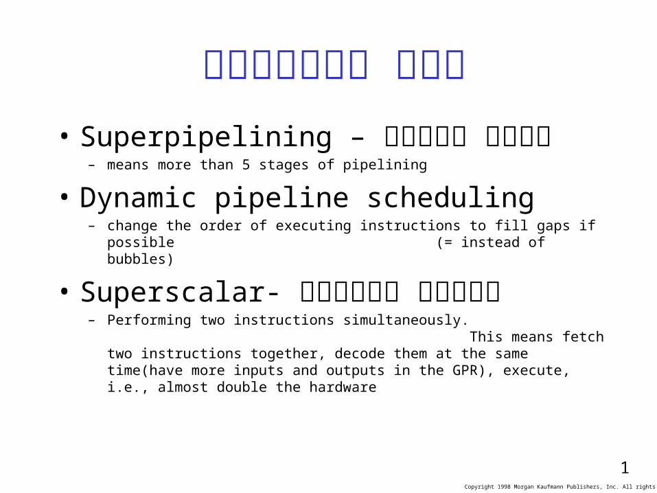
• Superpipelining – יותר שלבים – means more than 5 stages of pipelining
• Dynamic pipeline scheduling – change the order of executing instructions to fill gaps if possible (=
instead of bubbles)
• Superscalar- במקביל שלבים– Performing two instructions simultaneously. This
means fetch two instructions together, decode them at the same time(have more inputs and outputs in the GPR), execute, i.e., almost double the hardware
Copyright 1998 Morgan Kaufmann Publishers, Inc. All rights reserved.
2
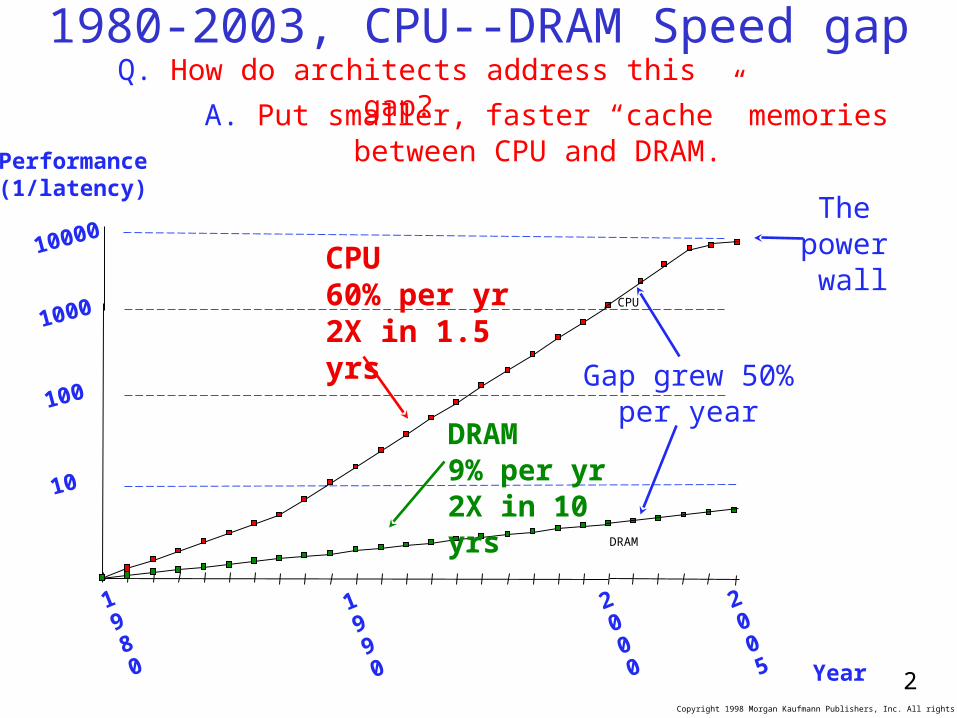
1980-2003, CPU--DRAM Speed gap
10
DRAM
CPU
Performance(1/latency)
100
1000
1980
2000
1990 Year
Gap grew 50% per year
Q. How do architects address this gap?
A. Put smaller, faster “cache” memories between CPU and DRAM.
10000The
power wall
2005
CPU60% per yr2X in 1.5 yrs
DRAM9% per yr2X in 10 yrs
Copyright 1998 Morgan Kaufmann Publishers, Inc. All rights reserved.
3
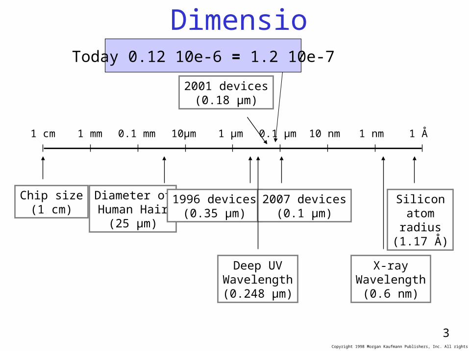
Dimensions
1 cm 1 mm 0.1 mm 10µm 1 µm 0.1 µm 10 nm 1 nm 1 Å
Chip size(1 cm)
Diameter ofHuman Hair
(25 µm)
1996 devices(0.35 µm)
2007 devices(0.1 µm)
Siliconatomradius
(1.17 Å)
Deep UVWavelength(0.248 µm)
X-rayWavelength
(0.6 nm)
2001 devices(0.18 µm)
Today 0.12 10e-6 = 1.2 10e-7
Copyright 1998 Morgan Kaufmann Publishers, Inc. All rights reserved.
4
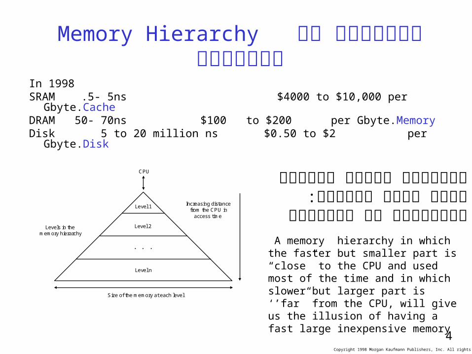
Memory Hierarchy היראכיה של הזיכרון
In 1998SRAM .5- 5ns $4000 to $10,000 per Gbyte. CacheDRAM 50- 70ns $100 to $200 per Gbyte. MemoryDisk 5 to 20 million ns $0.50 to $2 per Gbyte. Disk
CPU
Level n
Level 2
Level 1
Levels in thememory hierarchy
Increasing distance from the CPU in
access time
Size of the memory at each level
משתמשים רוצים זיכרון מהיר וזול הפתרון: הירארכיה של הזיכרון
A memory hierarchy in which the faster but smaller part is “close” to the CPU and used most of the time and in which slower but larger part is ‘’far” from the CPU, will give us the illusion of having a fast large inexpensive memory
Copyright 1998 Morgan Kaufmann Publishers, Inc. All rights reserved.
5
Caches Pipeline Relationship
WB
Data
Ad
der
IF/ID
ALU
Mem
ory
Reg File
MU
X
Data
Mem
ory
MU
X
SignExtend
Zero? MEM
/WB
EX
/MEM
4
Ad
der
Next SEQ PC
RD RD RD
Next PC
Addre
ss
RS1
RS2
Imm
MU
X
ID/E
X
I-$ D-$
Memory
Copyright 1998 Morgan Kaufmann Publishers, Inc. All rights reserved.
6
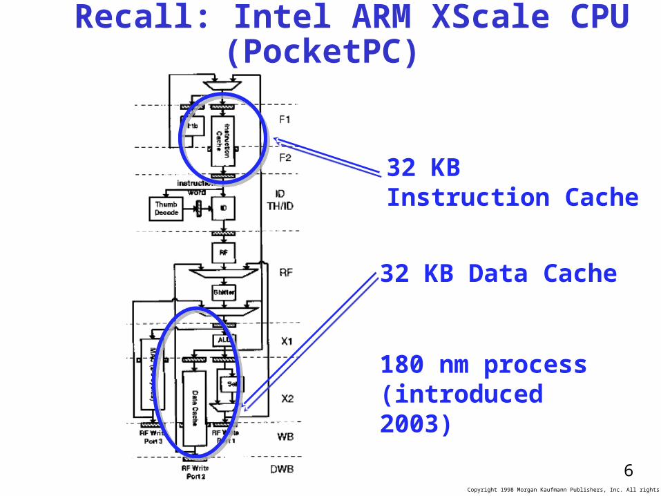
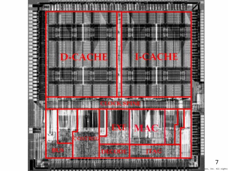
Recall: Intel ARM XScale CPU (PocketPC)
32 KB Instruction Cache
32 KB Data Cache
180 nm process (introduced 2003)
Copyright 1998 Morgan Kaufmann Publishers, Inc. All rights reserved.
7
Copyright 1998 Morgan Kaufmann Publishers, Inc. All rights reserved.
8
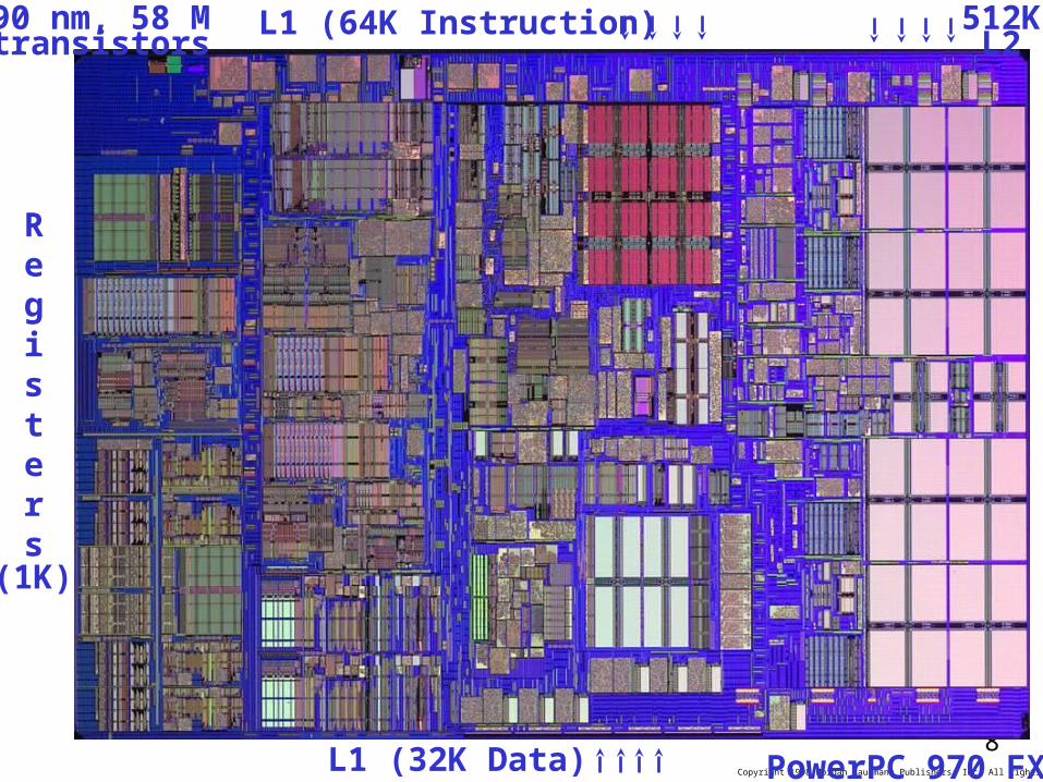
(1K)
Registers
L1 (64K Instruction)
L1 (32K Data)
512KL2
90 nm, 58 M transistors
PowerPC 970 FX
Copyright 1998 Morgan Kaufmann Publishers, Inc. All rights reserved.
Dunnington Intel 6 cores
• http://www.hardwarezone.com.au/reviews/view.php?cid=2&id=2516
9
Copyright 1998 Morgan Kaufmann Publishers, Inc. All rights reserved.
10
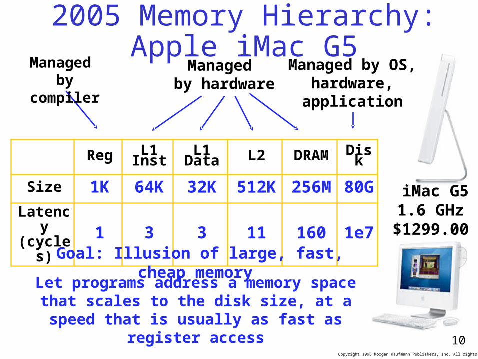
2005 Memory Hierarchy: Apple iMac G5
iMac G51.6 GHz$1299.00
Reg L1 Inst
L1 Data L2 DRAM Disk
Size 1K 64K 32K 512K 256M 80G
Latency(cycles) 1 3 3 11 160 1e7
Let programs address a memory space that scales to the disk size, at
a speed that is usually as fast as register access
Managed by compiler
Managed by hardware
Managed by OS,hardware,application
Goal: Illusion of large, fast, cheap memory
Copyright 1998 Morgan Kaufmann Publishers, Inc. All rights reserved.
11
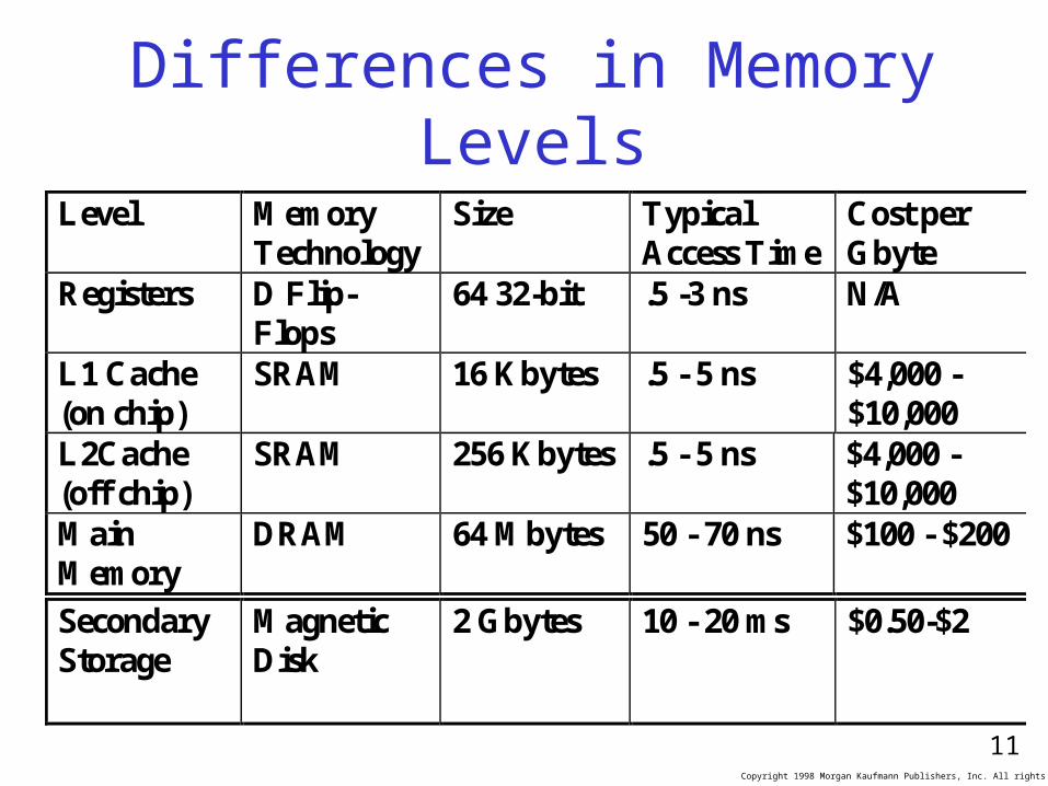
Differences in Memory Levels
Level Memory Technology
Size
Typical Access Time
Cost per Gbyte
Registers D Flip-Flops
64 32-bit .5 -3 ns N/A
L1 Cache (on chip)
SRAM 16 Kbytes .5 - 5 ns $4,000 - $10,000
L2Cache (off chip)
SRAM 256 Kbytes .5 - 5 ns $4,000 - $10,000
Main Memory
DRAM 64 Mbytes 50 - 70 ns $100 - $200
Secondary Storage
Magnetic Disk
2 Gbytes 10 - 20 ms $0.50-$2
Copyright 1998 Morgan Kaufmann Publishers, Inc. All rights reserved.
13
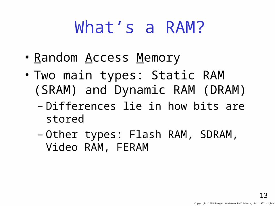
What’s a RAM?
• Random Access Memory
• Two main types: Static RAM (SRAM) and Dynamic RAM (DRAM)– Differences lie in how bits are stored– Other types: Flash RAM, SDRAM, Video RAM,
FERAM
Copyright 1998 Morgan Kaufmann Publishers, Inc. All rights reserved.
14
Basic RAM ArchitectureWord Lines
Bit Lines
Bit Cell
Sense Amplifier
Address
High
Low
Data
Copyright 1998 Morgan Kaufmann Publishers, Inc. All rights reserved.
15
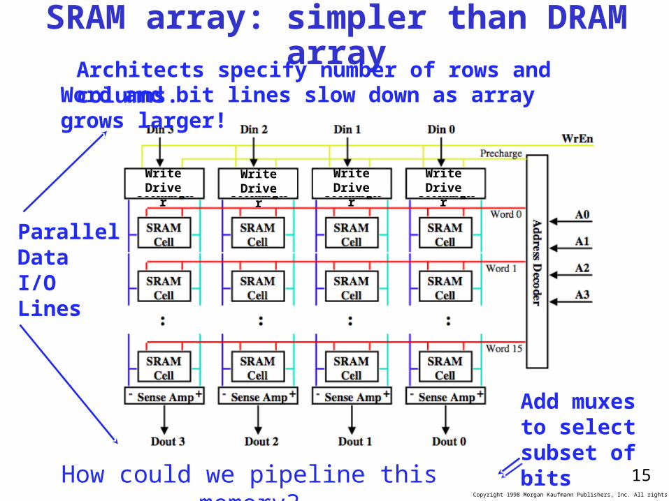
SRAM array: simpler than DRAM array
WriteDriver
WriteDriver
WriteDriver
WriteDriver
Word and bit lines slow down as array grows larger!
Architects specify number of rows and columns.
ParallelDataI/OLines
Add muxesto selectsubset of bitsHow could we pipeline this
memory?
Copyright 1998 Morgan Kaufmann Publishers, Inc. All rights reserved.
16
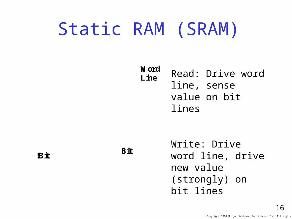
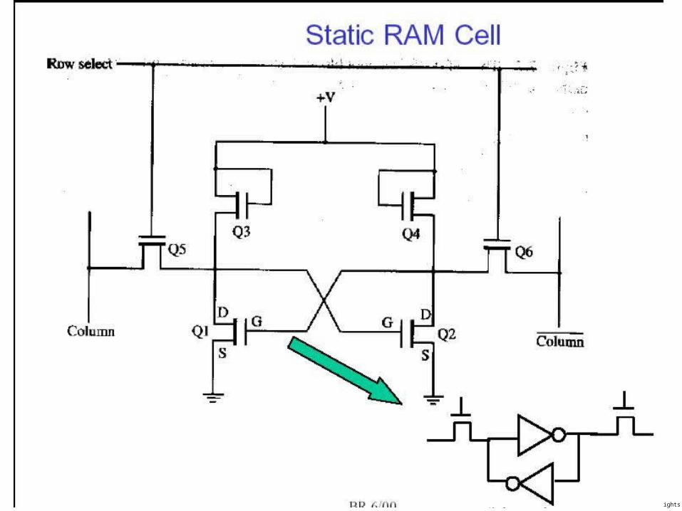
Static RAM (SRAM)
WordLine
Bit!Bit
Read: Drive word line, sense value on bit lines
Write: Drive word line, drive new value (strongly) on bit lines
Copyright 1998 Morgan Kaufmann Publishers, Inc. All rights reserved.
17
Copyright 1998 Morgan Kaufmann Publishers, Inc. All rights reserved.
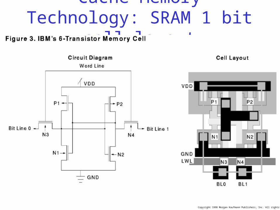
Cache Memory Technology: SRAM 1 bit cell layout
Copyright 1998 Morgan Kaufmann Publishers, Inc. All rights reserved.
Ref: http://www.msm.cam.ac.uk/dmg/teaching/m101999/Ch8/index.ht
m
Copyright 1998 Morgan Kaufmann Publishers, Inc. All rights reserved.
20
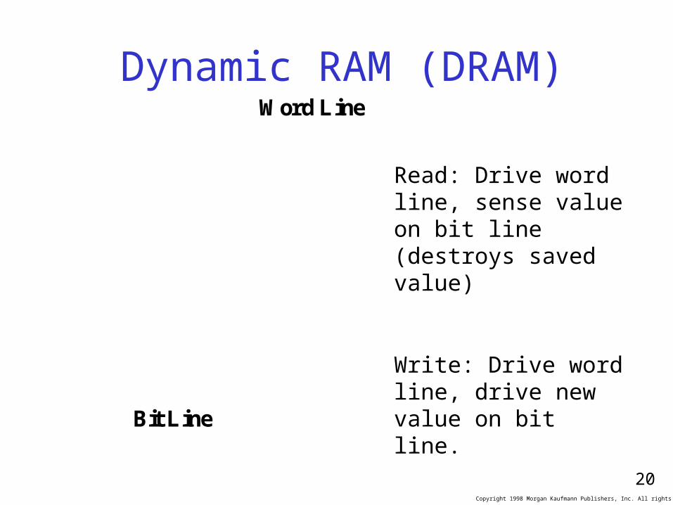
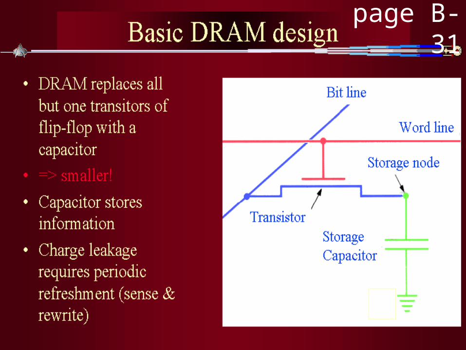
Dynamic RAM (DRAM)
Bit Line
Word Line
Read: Drive word line, sense value on bit line (destroys saved value)
Write: Drive word line, drive new value on bit line.
Copyright 1998 Morgan Kaufmann Publishers, Inc. All rights reserved.
see page B-31
Copyright 1998 Morgan Kaufmann Publishers, Inc. All rights reserved.
22
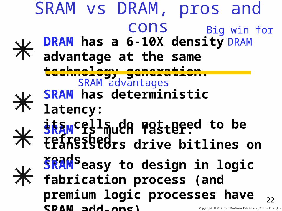
SRAM vs DRAM, pros and cons
DRAM has a 6-10X density advantage at the same technology generation.
Big win for DRAM
SRAM is much faster: transistors drive bitlines on reads.
SRAM easy to design in logic fabrication process (and premium logic processes have SRAM add-ons)
SRAM has deterministic latency: its cells do not need to be refreshed.
SRAM advantages
Copyright 1998 Morgan Kaufmann Publishers, Inc. All rights reserved.
23
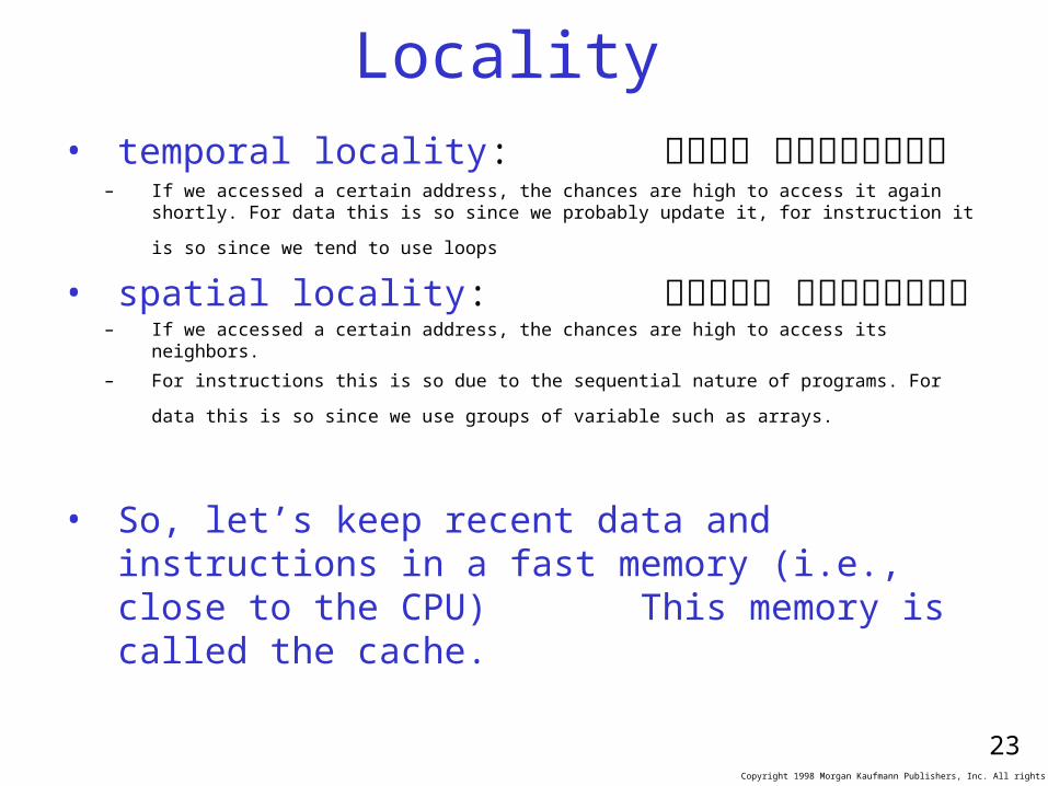
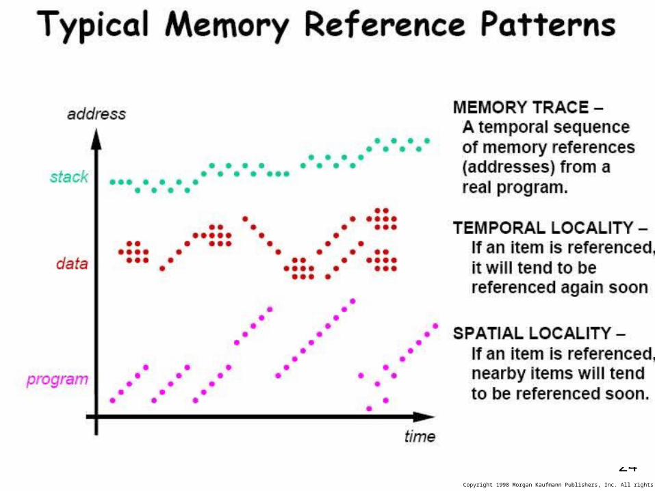
Locality
• temporal locality: לוקאליות בזמן – If we accessed a certain address, the chances are high to access it again shortly. For data
this is so since we probably update it, for instruction it is so since we tend to use loops
• spatial locality: לוקאליות במרחב– If we accessed a certain address, the chances are high to access its neighbors.
– For instructions this is so due to the sequential nature of programs. For data this is so
since we use groups of variable such as arrays.
• So, let’s keep recent data and instructions in a fast memory (i.e., close to the CPU) This memory is called the cache.
Copyright 1998 Morgan Kaufmann Publishers, Inc. All rights reserved.
24
Copyright 1998 Morgan Kaufmann Publishers, Inc. All rights reserved.
25
Copyright 1998 Morgan Kaufmann Publishers, Inc. All rights reserved.
26
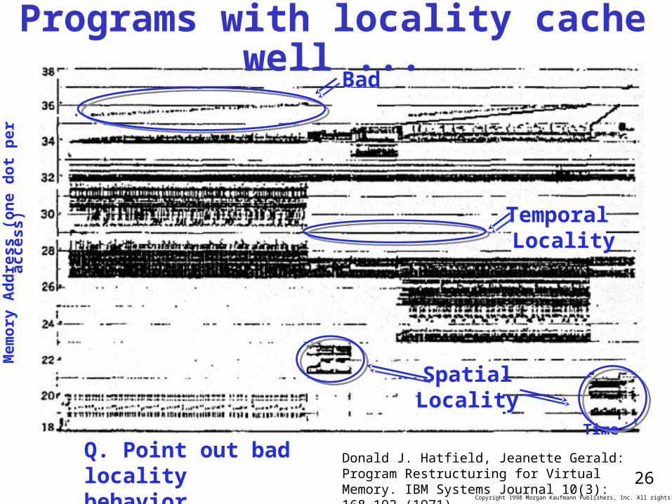
Programs with locality cache well ...
Donald J. Hatfield, Jeanette Gerald: Program Restructuring for Virtual Memory. IBM Systems Journal 10(3): 168-192 (1971)
Time
Mem
ory
Ad
dre
ss (
on
e d
ot
per
acc
ess)
Q. Point out bad locality behavior ...
SpatialLocality
Temporal Locality
Bad
Copyright 1998 Morgan Kaufmann Publishers, Inc. All rights reserved.
27
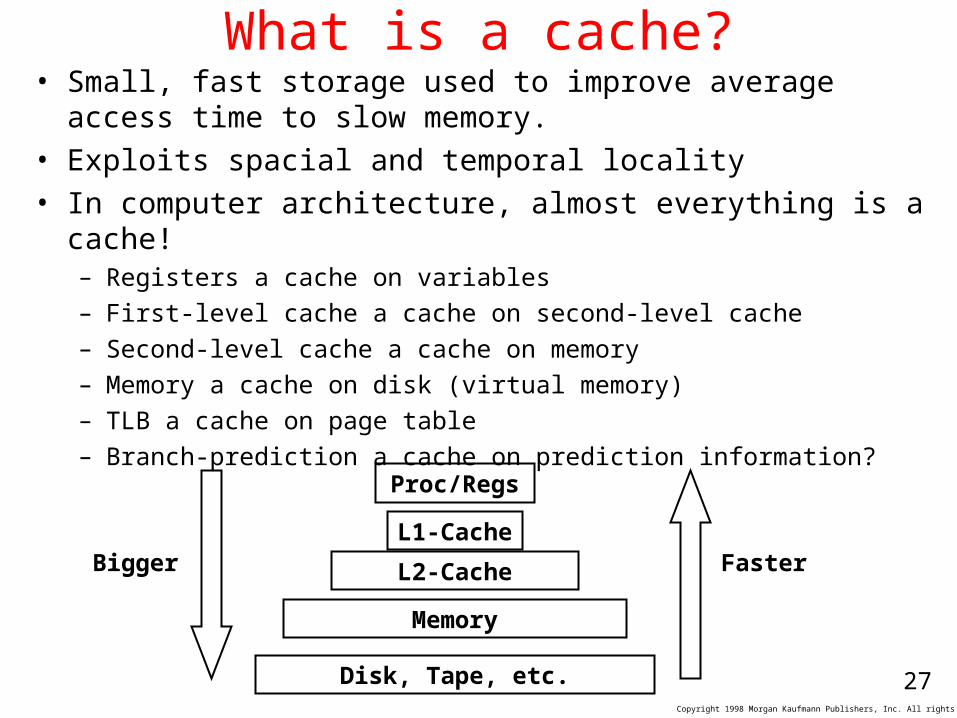
What is a cache?• Small, fast storage used to improve average access time to
slow memory.• Exploits spacial and temporal locality• In computer architecture, almost everything is a cache!
– Registers a cache on variables– First-level cache a cache on second-level cache– Second-level cache a cache on memory– Memory a cache on disk (virtual memory)– TLB a cache on page table– Branch-prediction a cache on prediction information?
Proc/RegsL1-
CacheL2-Cache
Memory
Disk, Tape, etc.
Bigger Faster
Copyright 1998 Morgan Kaufmann Publishers, Inc. All rights reserved.
28
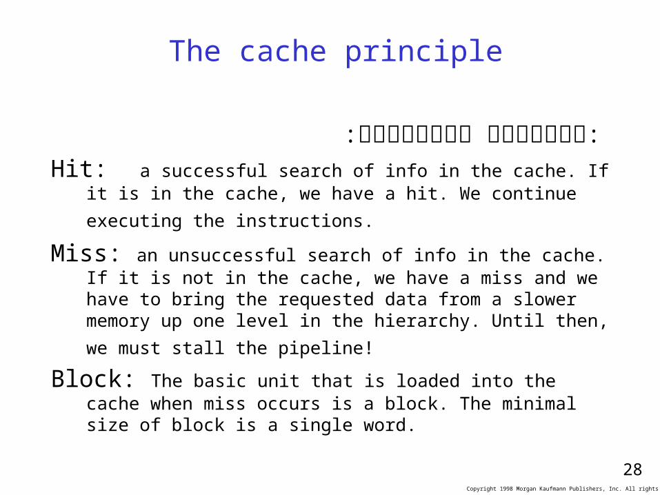
The cache principle
:המונחים המרכזיים:
Hit: a successful search of info in the cache. If it is in the
cache, we have a hit. We continue executing the instructions.
Miss: an unsuccessful search of info in the cache. If it is not in the cache, we have a miss and we have to bring the requested data from a slower memory up one level in the hierarchy.
Until then, we must stall the pipeline!
Block: The basic unit that is loaded into the cache when miss occurs is a block. The minimal size of block is a single word.
Copyright 1998 Morgan Kaufmann Publishers, Inc. All rights reserved.
29
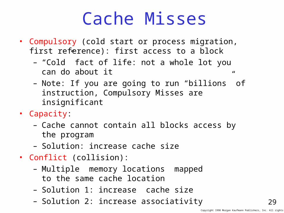
Cache Misses• Compulsory (cold start or process migration, first reference): first
access to a block
– “Cold” fact of life: not a whole lot you can do about it
– Note: If you are going to run “billions” of instruction, Compulsory Misses are insignificant
• Capacity:
– Cache cannot contain all blocks access by the program
– Solution: increase cache size
• Conflict (collision):
– Multiple memory locations mappedto the same cache location
– Solution 1: increase cache size
– Solution 2: increase associativity
• Coherence (Invalidation): other process (e.g., I/O) updates memory
Copyright 1998 Morgan Kaufmann Publishers, Inc. All rights reserved.
30
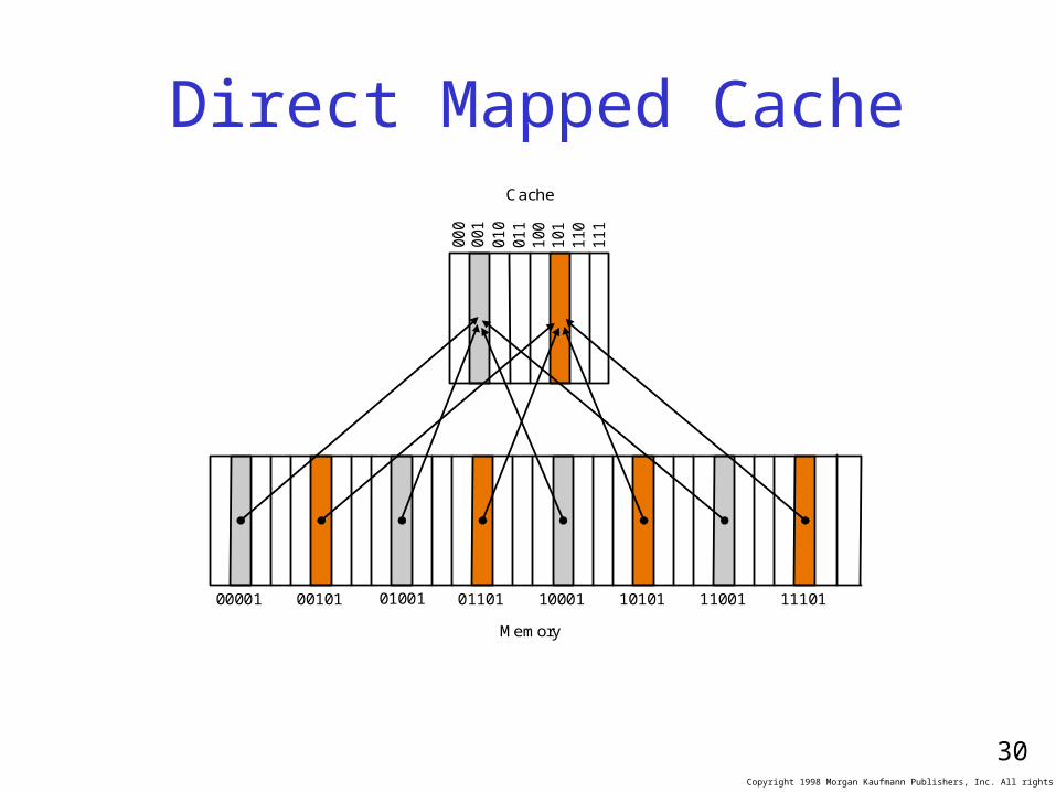
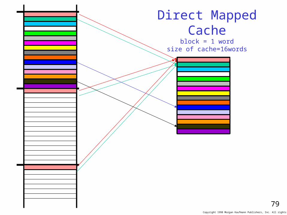
Direct Mapped Cache
00001 00101 01001 01101 10001 10101 11001 11101
000
Cache
Memory
001
010
011
100
101
110
111
Copyright 1998 Morgan Kaufmann Publishers, Inc. All rights reserved.
31
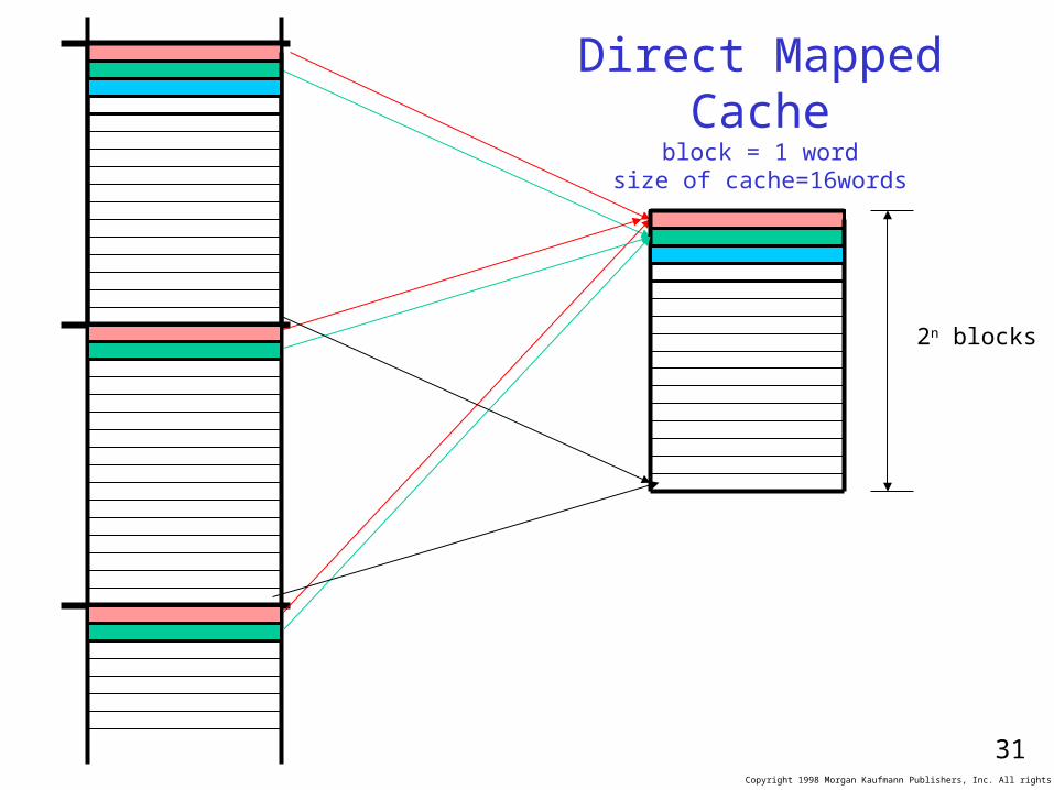
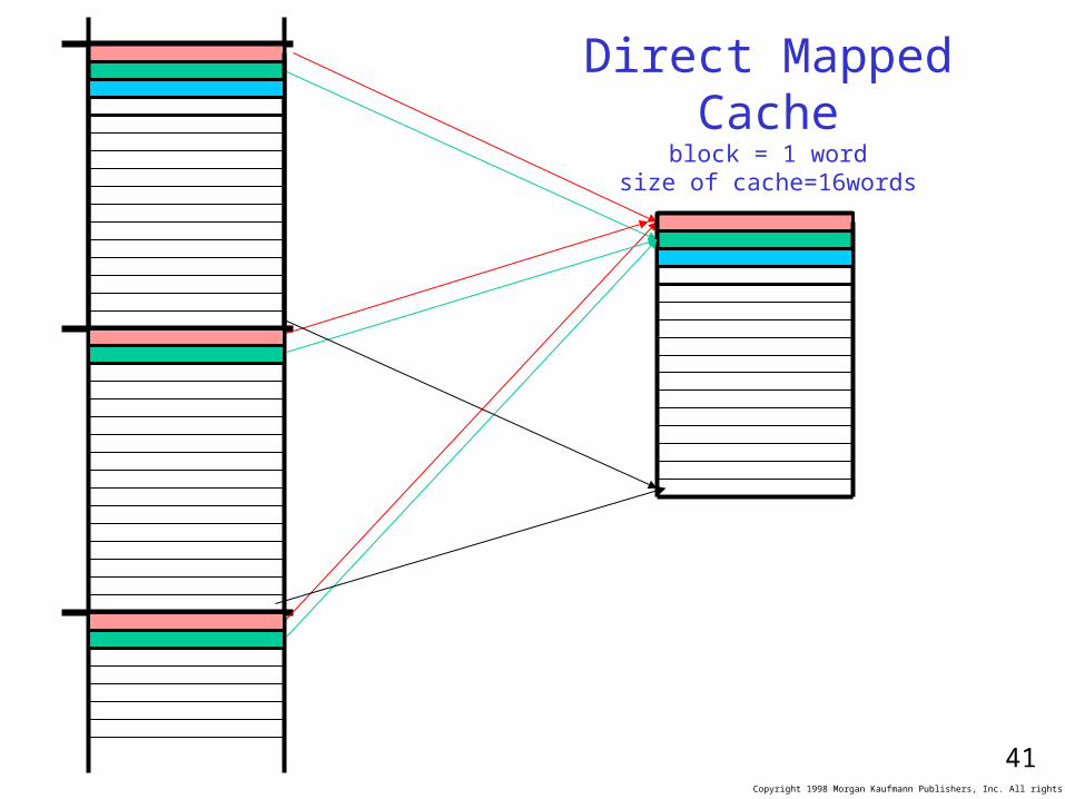
Direct Mapped Cacheblock = 1 word
size of cache=16words
2n blocks
Copyright 1998 Morgan Kaufmann Publishers, Inc. All rights reserved.
32
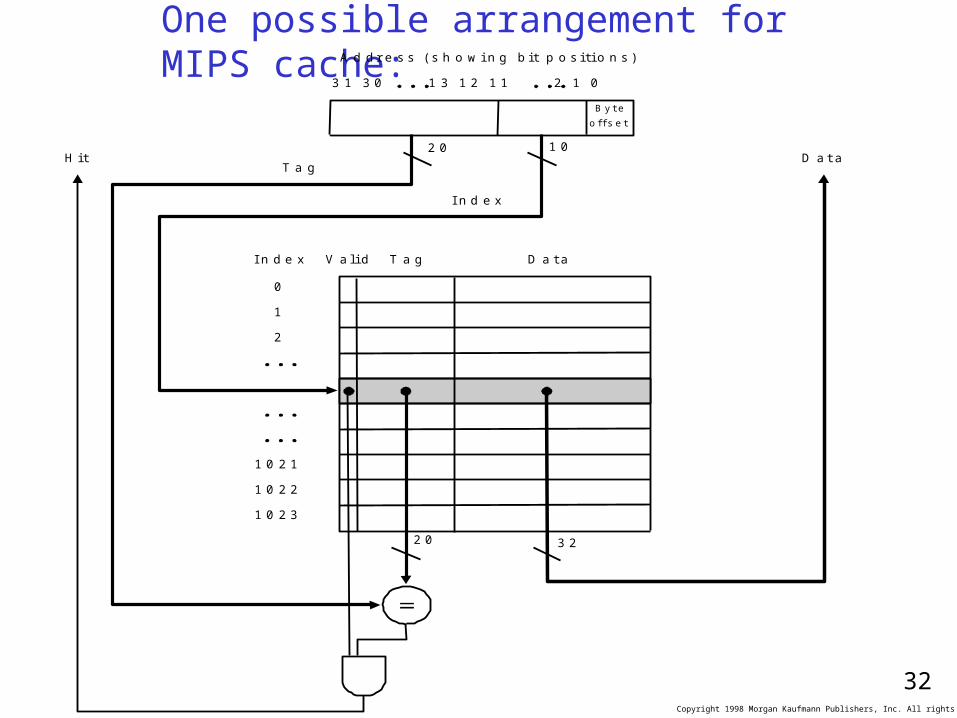
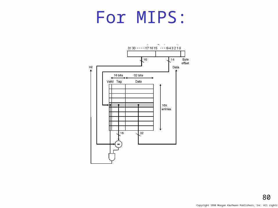
One possible arrangement for MIPS cache: A d d r e s s ( s h o w i n g b i t p o s i t i o n s )
2 0 1 0
B y t e
o f f s e t
V a l i d T a g D a t aI n d e x
0
1
2
1 0 2 1
1 0 2 2
1 0 2 3
T a g
I n d e x
H i t D a t a
2 0 3 2
3 1 3 0 1 3 1 2 1 1 2 1 0
Copyright 1998 Morgan Kaufmann Publishers, Inc. All rights reserved.
33
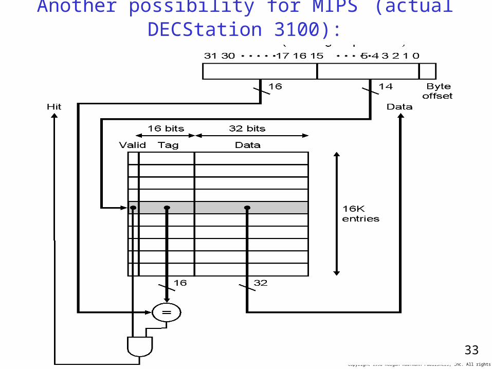
Another possibility for MIPS (actual DECStation 3100):
Copyright 1998 Morgan Kaufmann Publishers, Inc. All rights reserved.
34
For any 32 bit address CPU:
2n locations
A d d r e s s ( s h o w i n g b i t p o s i t i o n s )
30-n n
B y t e
o f f s e t
V a l i d T a g D a t a
T a g
I n d e x
H i t D a t a
3 2
3 1 3 n+2 n+1 2
1 0
I n d e x
0
1
2
2n -1
30-n
Copyright 1998 Morgan Kaufmann Publishers, Inc. All rights reserved.
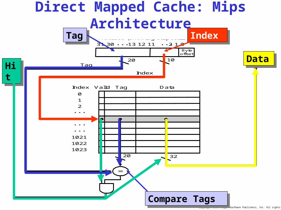
Address (showing bit positions)
20 10
Byteoffset
Valid Tag DataIndex
0
1
2
1021
1022
1023
Tag
Index
Hit Data
20 32
31 30 13 12 11 2 1 0TagTag IndexIndex
Direct Mapped Cache: Mips Architecture
DataData
Compare TagsCompare Tags
HitHit
Copyright 1998 Morgan Kaufmann Publishers, Inc. All rights reserved.
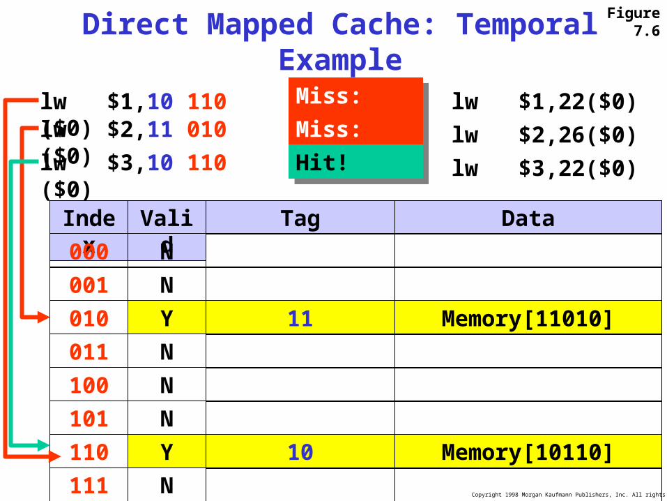
Direct Mapped Cache: Temporal Example
lw $1,22($0)lw $1,10 110 ($0)
lw $2,26($0)lw $2,11 010 ($0)
lw $3,22($0)lw $3,10 110 ($0)
Index Valid Tag Data
000 N
001 N
010 N
011 N
100 N
101 N
110 N
111 N
Y 10 Memory[10110]
Y 11 Memory[11010]
Miss: validMiss: valid
Miss: validMiss: valid
Hit!Hit!
Figure 7.6
Copyright 1998 Morgan Kaufmann Publishers, Inc. All rights reserved.
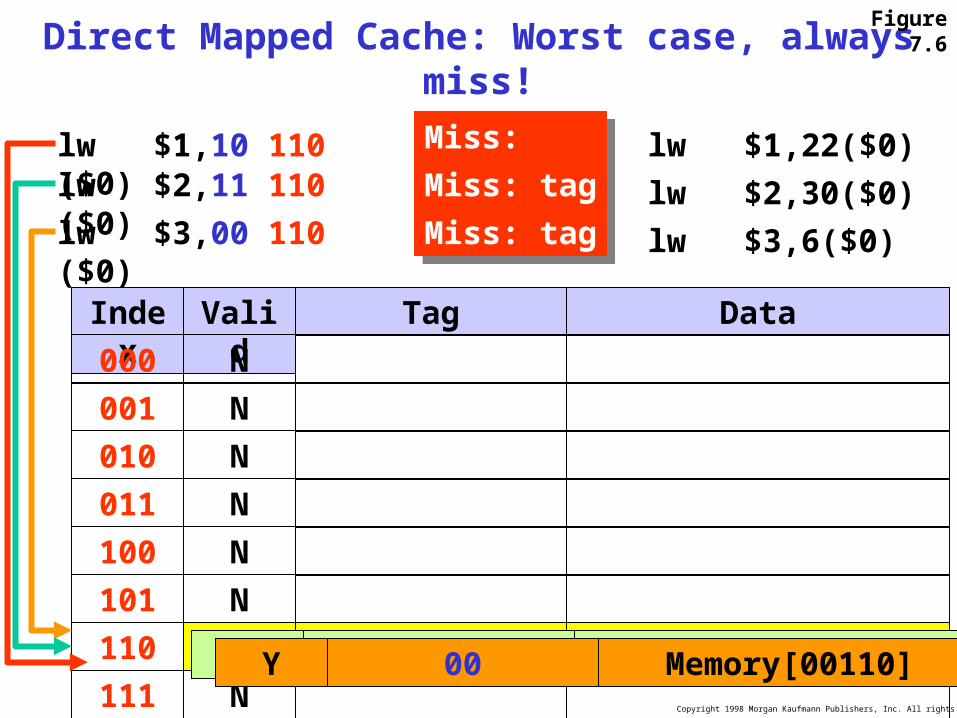
Direct Mapped Cache: Worst case, always miss!
lw $1,22($0)lw $1,10 110 ($0)
lw $2,30($0)lw $2,11 110 ($0)
lw $3,6($0)lw $3,00 110 ($0)
Index Valid Tag Data
000 N
001 N
010 N
011 N
100 N
101 N
110 N
111 N
Y 10 Memory[10110]Y 11 Memory[11110]
Miss: validMiss: valid
Miss: tagMiss: tag
Miss: tagMiss: tag
Figure 7.6
Y 00 Memory[00110]
Copyright 1998 Morgan Kaufmann Publishers, Inc. All rights reserved.
38
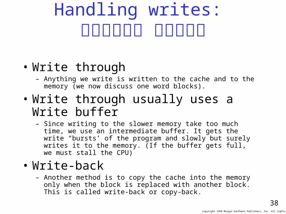
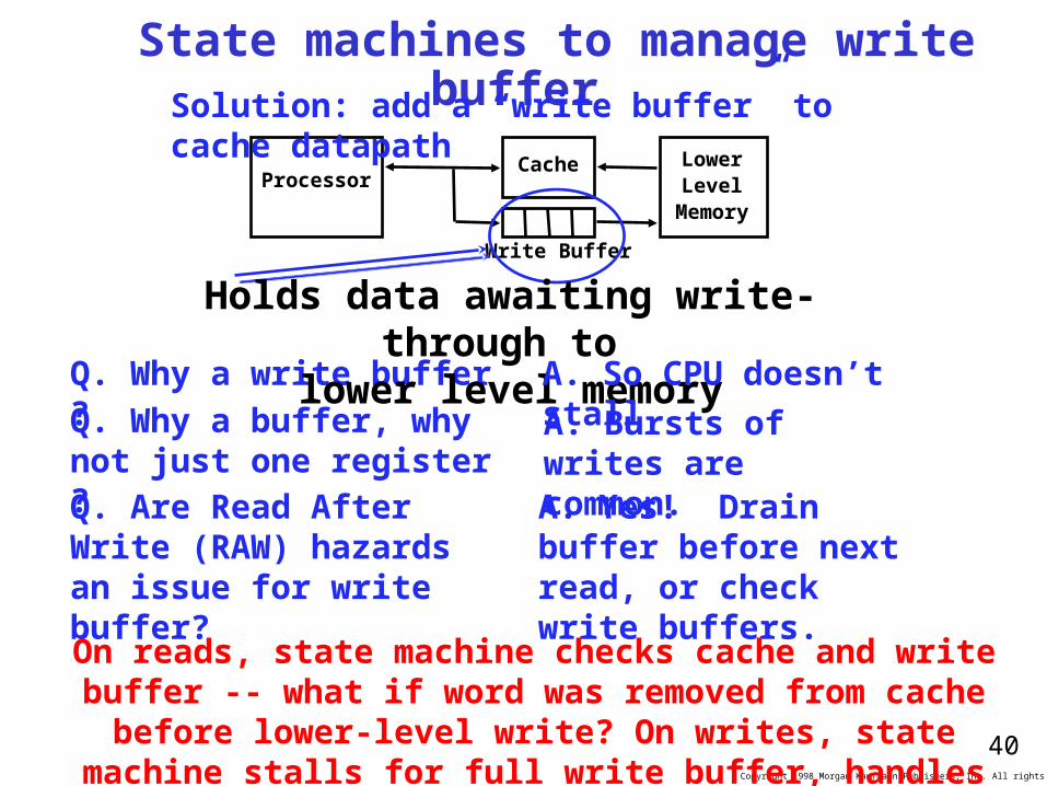
Handling writes: טיפול בכתיבה
• Write through – Anything we write is written to the cache and to the memory (we now
discuss one word blocks).
• Write through usually uses a Write buffer– Since writing to the slower memory take too much time, we use an
intermediate buffer. It gets the write “bursts’ of the program and slowly but surely writes it to the memory. (If the buffer gets full, we must stall the CPU)
• Write-back– Another method is to copy the cache into the memory only when the
block is replaced with another block. This is called write-back or copy-back.
Copyright 1998 Morgan Kaufmann Publishers, Inc. All rights reserved.
39
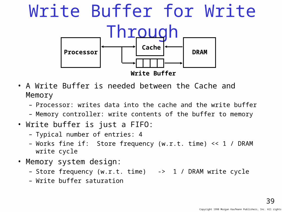
Write Buffer for Write Through
• A Write Buffer is needed between the Cache and Memory– Processor: writes data into the cache and the write buffer
– Memory controller: write contents of the buffer to memory
• Write buffer is just a FIFO:– Typical number of entries: 4
– Works fine if: Store frequency (w.r.t. time) << 1 / DRAM write cycle
• Memory system design:– Store frequency (w.r.t. time) -> 1 / DRAM write cycle
– Write buffer saturation
ProcessorCache
Write Buffer
DRAM
Copyright 1998 Morgan Kaufmann Publishers, Inc. All rights reserved.
40
State machines to manage write buffer
Q. Why a write buffer ?
ProcessorCache
Write Buffer
Lower Level
Memory
Holds data awaiting write-through to lower level memory
A. So CPU doesn’t stall Q. Why a buffer, why
not just one register ?A. Bursts of writes arecommon.Q. Are Read After
Write (RAW) hazards an issue for write buffer?
A. Yes! Drain buffer before next read, or check write buffers.
Solution: add a “write buffer” to cache datapath
On reads, state machine checks cache and write buffer -- what if word was removed from cache
before lower-level write? On writes, state machine stalls for full write buffer, handles write
buffer duplicates.
Copyright 1998 Morgan Kaufmann Publishers, Inc. All rights reserved.
41
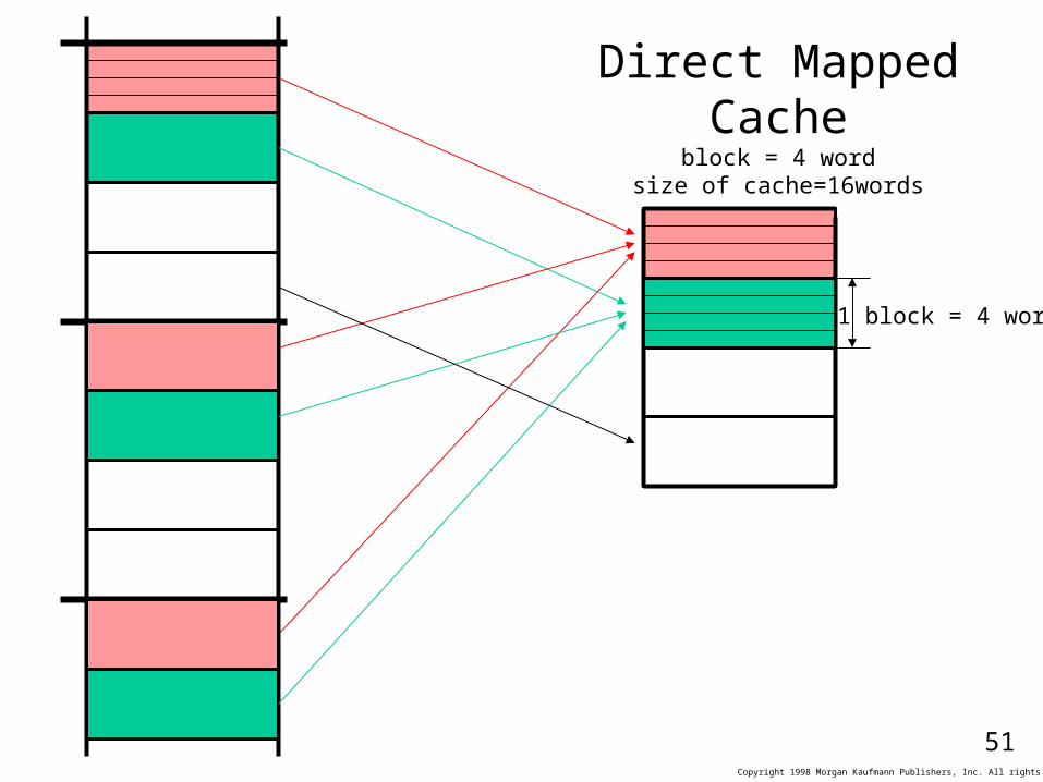
Direct Mapped Cacheblock = 1 word
size of cache=16words
Copyright 1998 Morgan Kaufmann Publishers, Inc. All rights reserved.
42
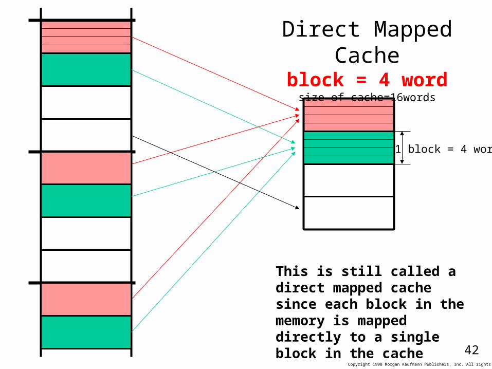
Direct Mapped Cacheblock = 4 word
size of cache=16words
This is still called a direct mapped cache since each block in the memory is mapped directly to a single block in the cache
1 block = 4 words
Copyright 1998 Morgan Kaufmann Publishers, Inc. All rights reserved.
43
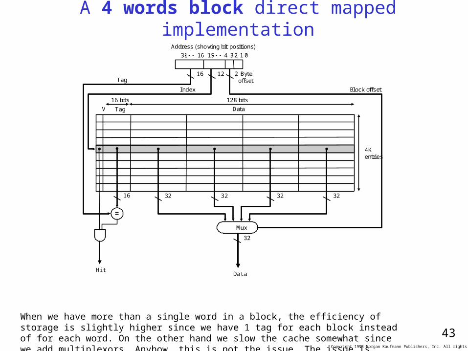
A 4 words block direct mapped implementationAddress (showing bit positions)
16 12 Byteoffset
V Tag Data
HitData
16 32
4Kentries
16 bits 128 bits
Mux
32 32 32
2
32
Block offsetIndex
Tag
31 16 15 4 32 1 0
When we have more than a single word in a block, the efficiency of storage is slightly higher since we have 1 tag for each block instead of for each word. On the other hand we slow the cache somewhat since we add multiplexors. Anyhow, this is not the issue. The issue is reducing miss rate
Copyright 1998 Morgan Kaufmann Publishers, Inc. All rights reserved.
44
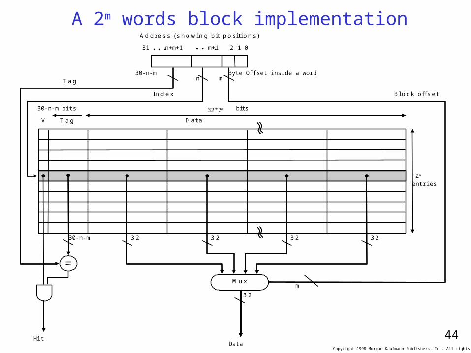
A 2m words block implementationA d d r e s s ( s h o w in g b it p o s i t i o n s )
30-n-mn
Byte Offset inside a word
V T a g D a ta
HitData
3 2
2n
entries
32*2m b i ts
M u x
3 2 3 2 3 2
m
3 2
B lo c k o f fs e tI n d e x
T a g
31
n+m+1 m+1 2 1 0
m
30-n-m bits
30-n-m
Copyright 1998 Morgan Kaufmann Publishers, Inc. All rights reserved.
45
1 KB
8 KB
16 KB
64 KB
256 KB
256
40%
35%
30%
25%
20%
15%
10%
5%
0%
Mis
s ra
te
64164
Block size (bytes)
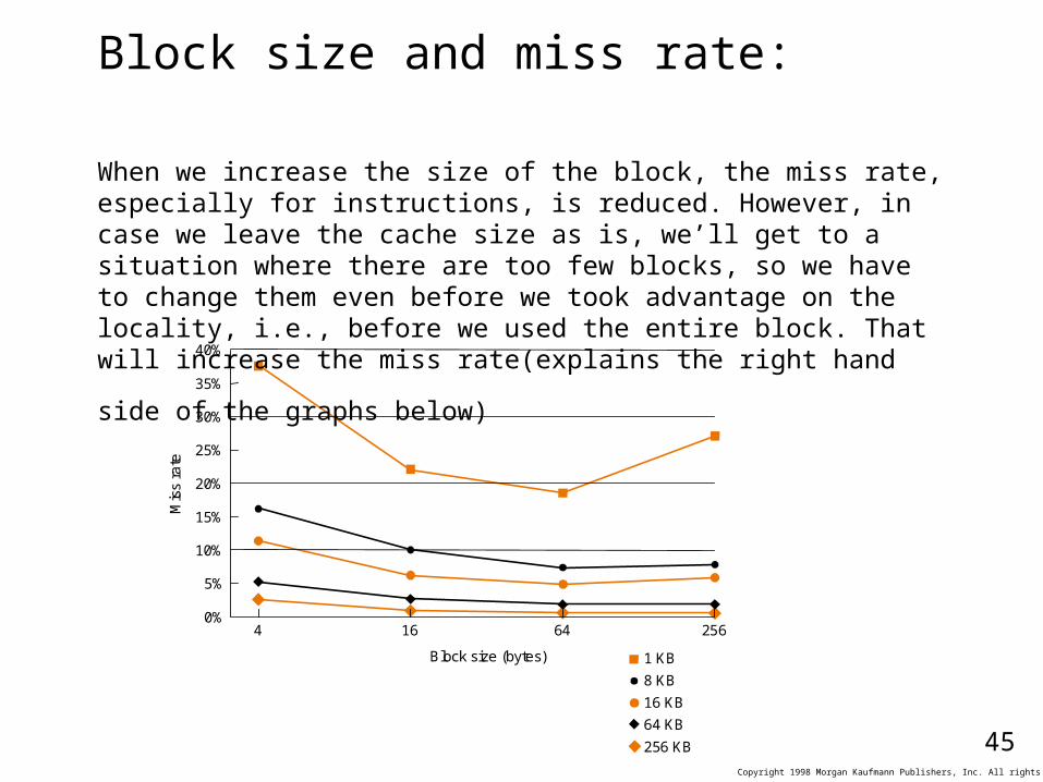
Block size and miss rate:
When we increase the size of the block, the miss rate, especially for instructions, is reduced. However, in case we leave the cache size as is, we’ll get to a situation where there are too few blocks, so we have to change them even before we took advantage on the locality, i.e., before we used the entire block. That will
increase the miss rate(explains the right hand side of the graphs below)
Copyright 1998 Morgan Kaufmann Publishers, Inc. All rights reserved.
46
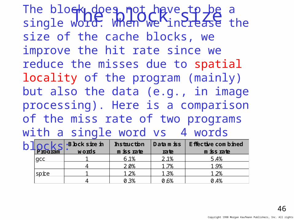
The block size
ProgramBlock size in
wordsInstruction miss rate
Data miss rate
Effective combined miss rate
gcc 1 6.1% 2.1% 5.4%4 2.0% 1.7% 1.9%
spice 1 1.2% 1.3% 1.2%4 0.3% 0.6% 0.4%
The block does not have to be a single word. When we increase the size of the cache blocks, we improve the hit rate since we reduce the misses due to spatial locality of the program (mainly) but also the data (e.g., in image processing). Here is a comparison of the miss rate of two programs with a single word vs 4 words blocks:
Copyright 1998 Morgan Kaufmann Publishers, Inc. All rights reserved.
47
Block Size (bytes)
Miss Rate
0%
5%
10%
15%
20%
25%
16
32
64
12
8
25
6
1K
4K
16K
64K
256K
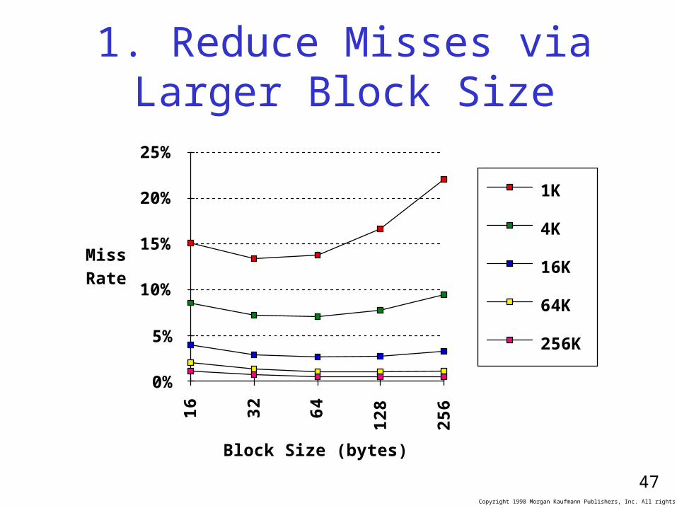
1. Reduce Misses via Larger Block Size
Copyright 1998 Morgan Kaufmann Publishers, Inc. All rights reserved.
48
Block size and write:
When we have more than a single word in a block, then when we write (a single word) into a block, we must first read the entire block from the memory (unless its already in the cache) and only then write to the cache and to the memory.
If we had the block in the cache, the process is exactly as it was for a single word block cache.
Separate instruction and data caches
Note that usually we have separate instruction and data caches. Having a single cache for both could give some flexibility since we have sometimes more room for data but the 2 separate caches have twice the bandwidth, I.e., we can read both at the same time (2 times faster). That is why most CPUs use separate instruction and data caches.
Copyright 1998 Morgan Kaufmann Publishers, Inc. All rights reserved.
49
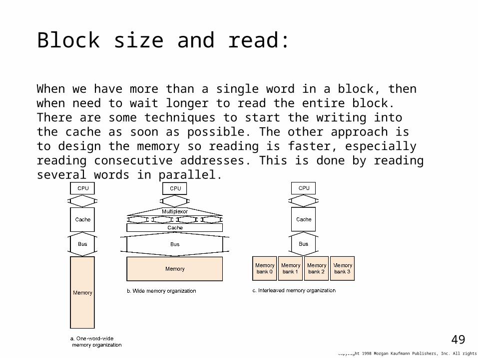
Block size and read:
When we have more than a single word in a block, then when need to wait longer to read the entire block. There are some techniques to start the writing into the cache as soon as possible. The other approach is to design the memory so reading is faster, especially reading consecutive addresses. This is done by reading several words in parallel.
Copyright 1998 Morgan Kaufmann Publishers, Inc. All rights reserved.
50
Faster CPUs need better cachesIt is shown in the book (section 7.3 pp. 565-567) that when we improve the CPU (shorten the CPI or the CK period) but leave the cache as is, the percentage of miss penaly is increased. This means that we need better caches for faster CPUs. Better means we should reduce the miss rate and reduce the miss penalty.
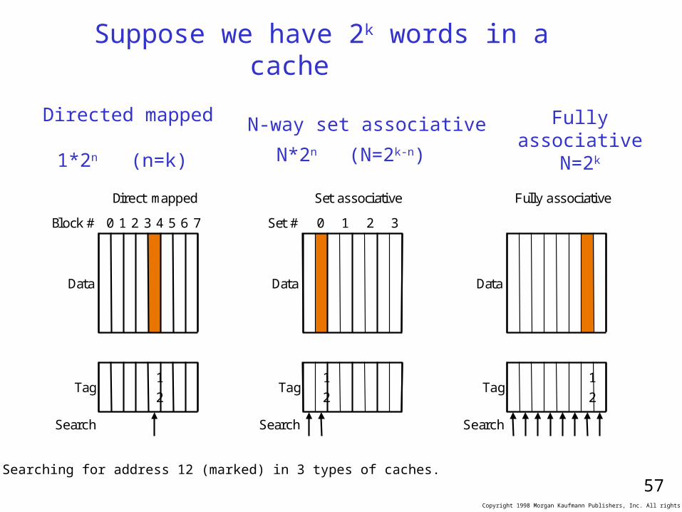
Reducing the miss rateThis is done by letting the cache more flexibility in keeping data.
So far we allowed a memory block to be mapped to a single block in cache. We called it a direct mapped cache. There is no flexibility here. The most flexible scheme is that a block can be store at any of the cache blocks. That way, we can keep some frequently used blocked that always competed on the same cache block in direct mapped block implementation. Such a flexible scheme is called fully associative cache. In a fully associative cache the tag should be compared to all cache entries.
We have also a compromise called “N-way set associative” cache. Here each memory block is mapped to one of an N blocks of the cache.
Note that for caches having more than 1 possible mapping, we should employ some replacement policy. (LRU or Random are used)
Copyright 1998 Morgan Kaufmann Publishers, Inc. All rights reserved.
51
Direct Mapped Cacheblock = 4 word
size of cache=16words
1 block = 4 words
Copyright 1998 Morgan Kaufmann Publishers, Inc. All rights reserved.
52
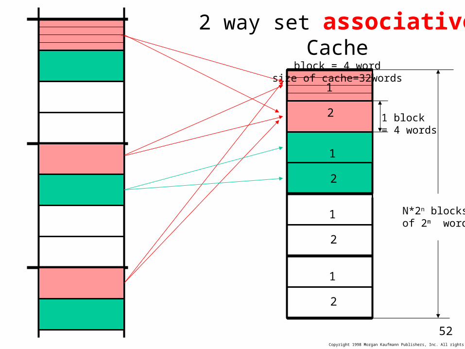
2 way set associative Cacheblock = 4 word
size of cache=32words
1 block = 4 words
1
2
1
2
1
2
1
2
N*2n blocksof 2m words
Copyright 1998 Morgan Kaufmann Publishers, Inc. All rights reserved.
53
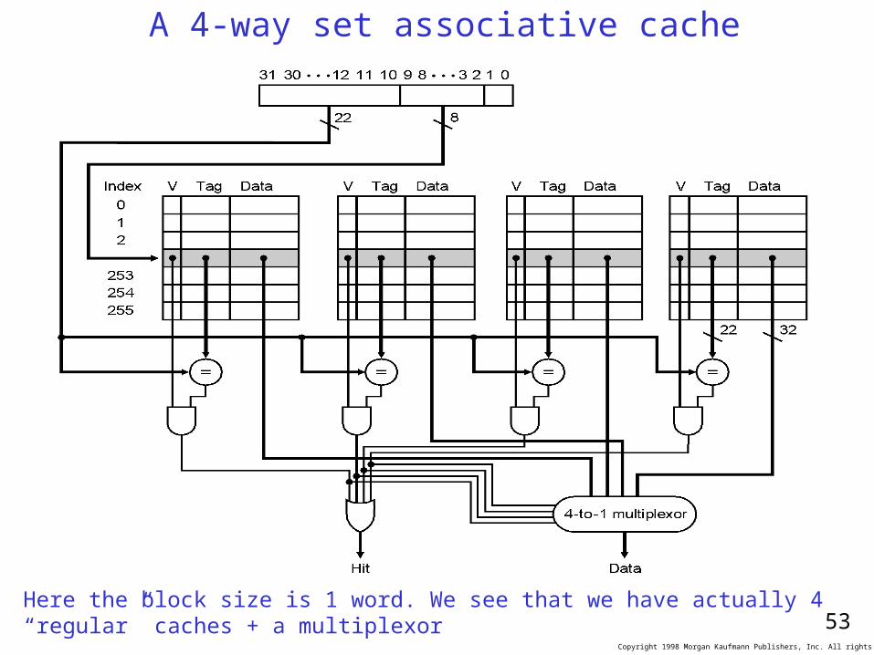
A 4-way set associative cache
Here the block size is 1 word. We see that we have actually 4 “regular” caches + a multiplexor
Copyright 1998 Morgan Kaufmann Publishers, Inc. All rights reserved.
54
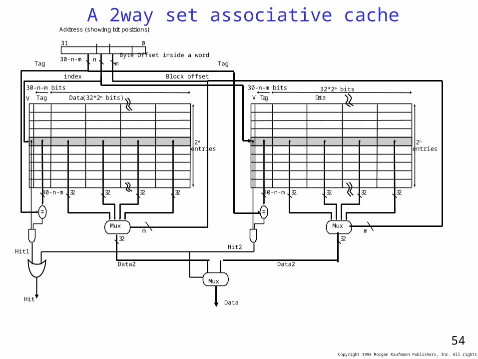
A 2way set associative cacheAddress (showing bit positions)
30-n-m nByte Offset inside a word
V Tag Data
Hit1
Data2
32
2n
entries
(32*2m bits)
32 32 32
m
32
Block offsetindex
Tag
31
0
m
30-n-m bits
30-n-m
V Tag Data
Hit2
Data2
32
2n
entries
Mux
32 32 32
32m
30-n-m bits
30-n-m
Tag
32*2m bits
Data
Mux
Mux
Hit
Copyright 1998 Morgan Kaufmann Publishers, Inc. All rights reserved.
55
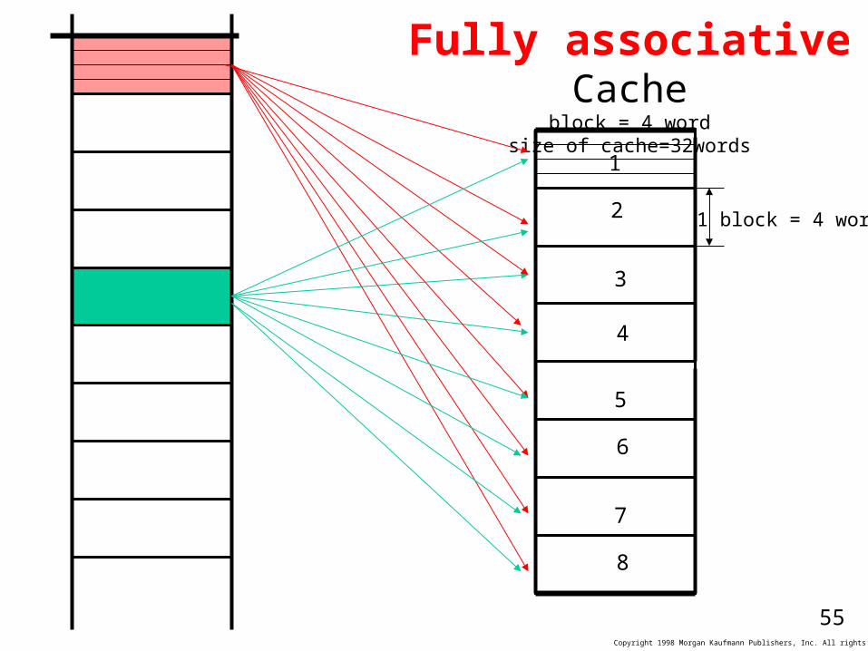
Fully associative Cacheblock = 4 word
size of cache=32words
1 block = 4 words
3
4
1
2
5
6
7
8
Copyright 1998 Morgan Kaufmann Publishers, Inc. All rights reserved.
56
A fully associative
cache
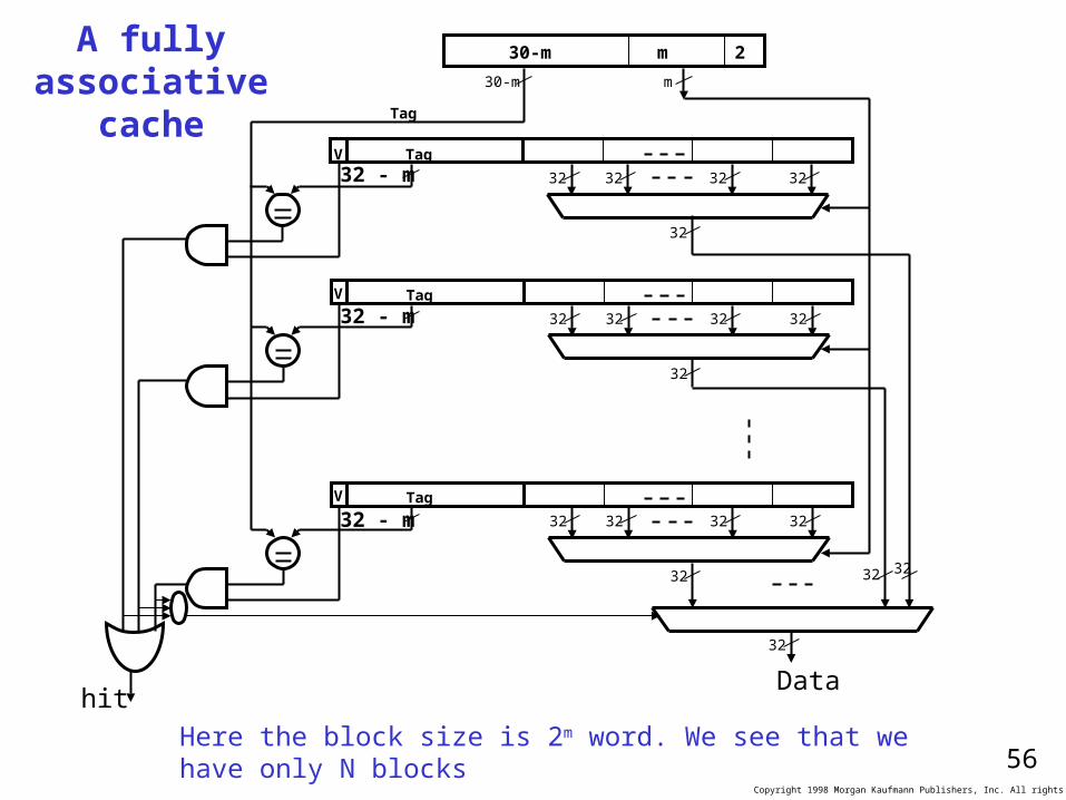
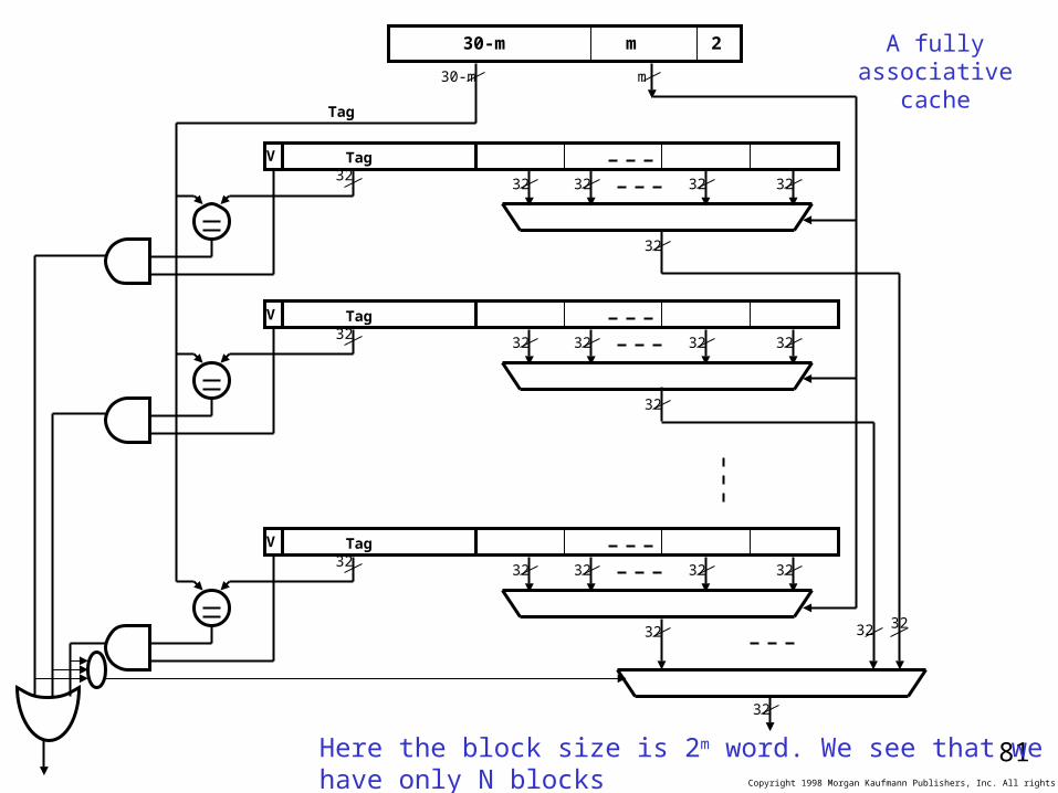
Here the block size is 2m word. We see that we have only N blocks
30-m 2
m
Tag
30-m
m
3232
32 32 32 32
TagV
32
32 32 32 3232 - mTagV
32
32 32 32 32
TagV
32
32
hitData
32 - m
32 - m
Copyright 1998 Morgan Kaufmann Publishers, Inc. All rights reserved.
57
N-way set associative
N*2n (N=2k-n)
1
2Tag
Data
Block # 0 1 2 3 4 5 6 7
Search
Direct mapped
1
2Tag
Data
Set # 0 1 2 3
Search
Set associative
1
2Tag
Data
Search
Fully associative
Directed mapped 1*2n (n=k)
Fully associativeN=2k
Suppose we have 2k words in a cache
Searching for address 12 (marked) in 3 types of caches.
Copyright 1998 Morgan Kaufmann Publishers, Inc. All rights reserved.
58
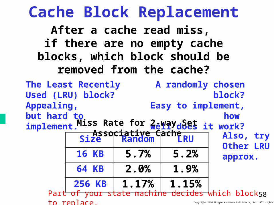
Cache Block Replacement After a cache read miss,
if there are no empty cache blocks, which block should be removed
from the cache?A randomly chosen
block?Easy to implement,
how well does it work?
The Least Recently Used (LRU) block? Appealing,but hard to implement.Miss Rate for 2-way Set Associative Cache
Also, tryOther LRUapprox.
Part of your state machine decides which block to replace.
Size Random LRU
16 KB 5.7% 5.2%64 KB 2.0% 1.9%
256 KB 1.17% 1.15%
Copyright 1998 Morgan Kaufmann Publishers, Inc. All rights reserved.
59
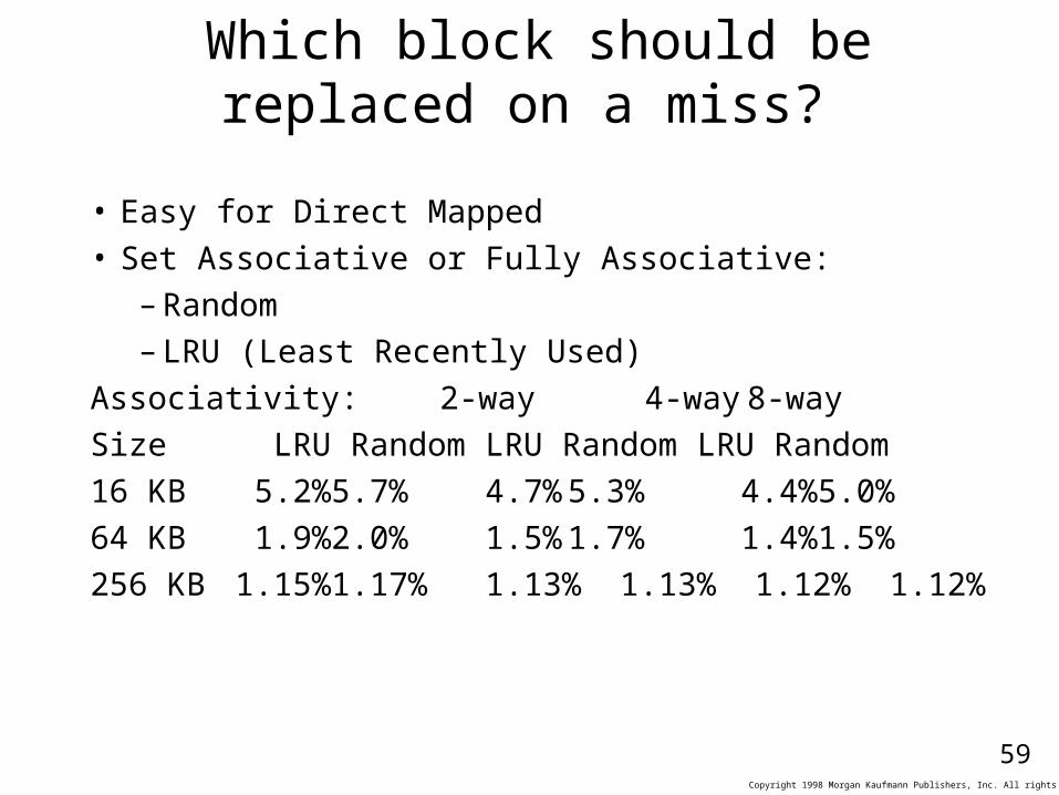
Which block should be replaced on a miss?
• Easy for Direct Mapped
• Set Associative or Fully Associative:
– Random
– LRU (Least Recently Used)
Associativity: 2-way 4-way 8-way
Size LRU Random LRU Random LRU Random
16 KB 5.2% 5.7% 4.7% 5.3% 4.4% 5.0%
64 KB 1.9% 2.0% 1.5% 1.7% 1.4% 1.5%
256 KB 1.15% 1.17% 1.13% 1.13% 1.12% 1.12%
Copyright 1998 Morgan Kaufmann Publishers, Inc. All rights reserved.
60
Faster CPUs need better cachesBetter means we should reduce the miss rate. For that we used 4 set associative cache.
Better also means reduce the miss penalty.
Reducing the miss penaltyThis is done by using 2 levels cache. The first cache will be on the same chip as the CPU, actually it is a part of the CPU. It is very fast (1-2ns=less than 1 ck cycle) it is small, the block is also small, so it can be 4-way set associative. The level 2 cache is out of the chip 10 times slower but still 10 times faster than the memory (DRAM). It has larger block almost always 2-way set associative or direct mapped. Mainly aimed to reduce the read penalty. Analyzing such caches is complicated. Ususally simulations are required.
An optimal single level cache is usually larger and slower than the level1 cache and faster and smaller than the level2 cache.
Note that usually we have separate instruction and data caches.
Copyright 1998 Morgan Kaufmann Publishers, Inc. All rights reserved.
62
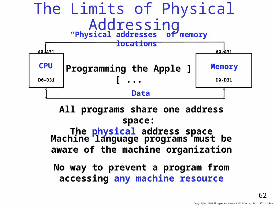
The Limits of Physical Addressing
CPU Memory
A0-A31 A0-A31
D0-D31 D0-D31
“Physical addresses” of memory locations
Data
All programs share one address space: The physical address space
No way to prevent a program from accessing any machine resource
Machine language programs must beaware of the machine organization
Programming the Apple ][ ...
Copyright 1998 Morgan Kaufmann Publishers, Inc. All rights reserved.
63
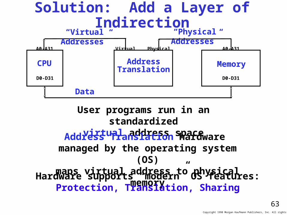
Solution: Add a Layer of Indirection
CPU Memory
A0-A31 A0-A31
D0-D31 D0-D31
Data
User programs run in an standardizedvirtual address space
Address Translation hardware managed by the operating system (OS)
maps virtual address to physical memory
“Physical Addresses”
AddressTranslation
Virtual Physical
“Virtual Addresses”
Hardware supports “modern” OS features:Protection, Translation, Sharing
Copyright 1998 Morgan Kaufmann Publishers, Inc. All rights reserved.
64
Virtual Memory
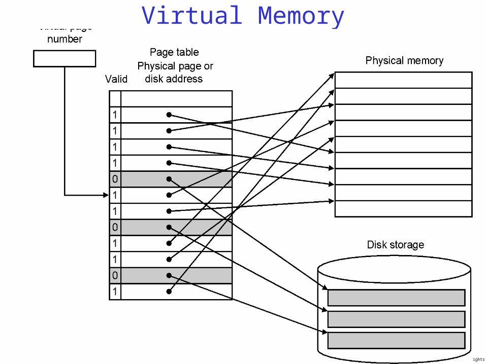
Copyright 1998 Morgan Kaufmann Publishers, Inc. All rights reserved.
65
Virtual Memory
Copyright 1998 Morgan Kaufmann Publishers, Inc. All rights reserved.
66
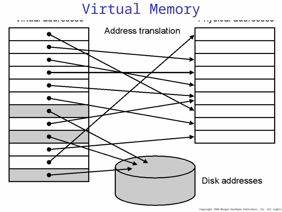
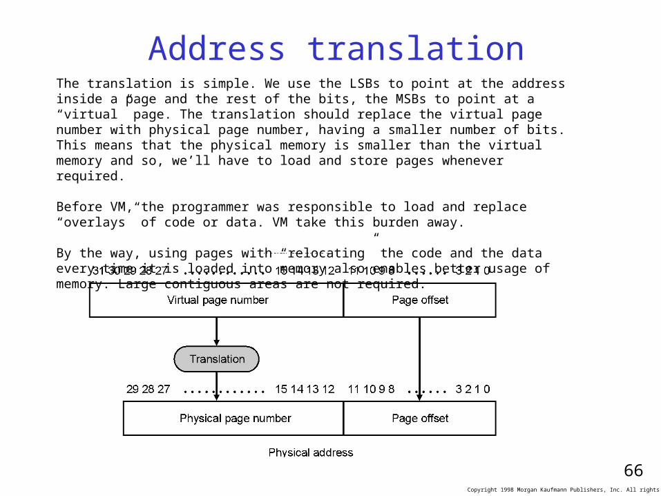
Address translationThe translation is simple. We use the LSBs to point at the address inside a page and the rest of the bits, the MSBs to point at a “virtual” page. The translation should replace the virtual page number with physical page number, having a smaller number of bits. This means that the physical memory is smaller than the virtual memory and so, we’ll have to load and store pages whenever required.
Before VM, the programmer was responsible to load and replace “overlays” of code or data. VM take this burden away.
By the way, using pages with “relocating” the code and the data every time it is loaded into memory also enables better usage of memory. Large contiguous areas are not required.
Copyright 1998 Morgan Kaufmann Publishers, Inc. All rights reserved.
67
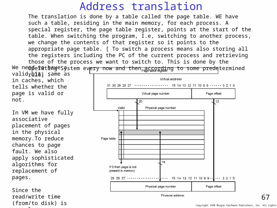
Address translationThe translation is done by a table called the page table. WE have such a table, residing in the main memory, for each process. A special register, the page table register, points at the start of the table. When switching the program, I.e, switching to another process, we change the contents of that register so it points to the appropriate page table. [ To switch a process means also storing all the registers including the PC of the current process and retrieving those of the process we want to switch to. This is done by the Operating System every now and then according to some predetermined rule] .
We need to have a valid bit, same as in caches, which tells whether the page is valid or not.
In VM we have fully associative placement of pages in the physical memory.To reduce chances to page fault. We also apply sophisticated algorithms for replacement of pages.
Since the read/write time (from/to disk) is very long, we use s/w mechanism instead of h/w (used in caches). Also, we use write-back scheme and not write-through.
Copyright 1998 Morgan Kaufmann Publishers, Inc. All rights reserved.
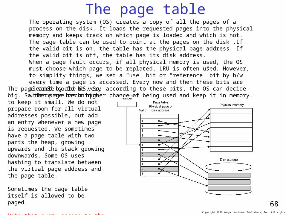
68
The page tableThe operating system (OS) creates a copy of all the pages of a process on the disk. It loads the requested pages into the physical memory and keeps track on which page is loaded and which is not. The page table can be used to point at the pages on the disk .If the valid bit is on, the table has the physical page address. If the valid bit is off, the table has its disk address. When a page fault occurs, if all physical memory is used, the OS must choose which page to be replaced. LRU is often used. However, to simplify things, we set a “use” bit or “reference” bit by h/w every time a page is accessed. Every now and then these bits are cleared by the OS. So, according to these bits, the OS can decide which page has a higher chance of being used and keep it in memory.
The page table could be very big. So there are technique to keep it small. We do not prepare room for all virtual addresses possible, but add an entry whenever a new page is requested. We sometimes have a page table with two parts the heap, growing upwards and the stack growing downwards. Some OS uses hashing to translate between the virtual page address and the page table.
Sometimes the page table itself is allowed to be paged.
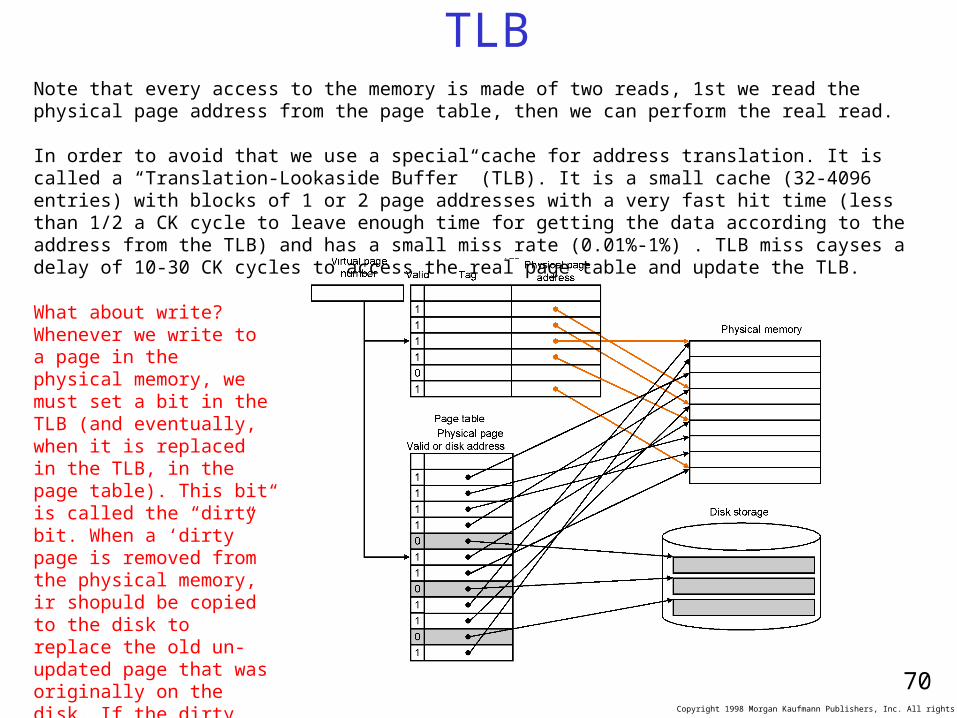
Note that every access to the memory is made of two reads, 1st we read the physical page address from the page table, then we can perform the real read.
Copyright 1998 Morgan Kaufmann Publishers, Inc. All rights reserved.
69
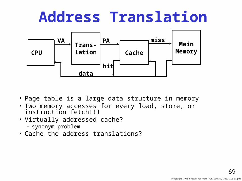
Address Translation
• Page table is a large data structure in memory• Two memory accesses for every load, store, or instruction fetch!!!• Virtually addressed cache?
– synonym problem• Cache the address translations?
CPUTrans-lation Cache
MainMemory
VA PA miss
hitdata
Copyright 1998 Morgan Kaufmann Publishers, Inc. All rights reserved.
70
TLBNote that every access to the memory is made of two reads, 1st we read the physical page address from the page table, then we can perform the real read.
In order to avoid that we use a special cache for address translation. It is called a “Translation-Lookaside Buffer” (TLB). It is a small cache (32-4096 entries) with blocks of 1 or 2 page addresses with a very fast hit time (less than 1/2 a CK cycle to leave enough time for getting the data according to the address from the TLB) and has a small miss rate (0.01%-1%) . TLB miss cayses a delay of 10-30 CK cycles to access the real page table and update the TLB.
What about write? Whenever we write to a page in the physical memory, we must set a bit in the TLB (and eventually, when it is replaced in the TLB, in the page table). This bit is called the “dirty” bit. When a ‘dirty” page is removed from the physical memory, ir shopuld be copied to the disk to replace the old un-updated page that was originally on the disk. If the dirty bit is off, no copy is required since the original page is untoutched.
Copyright 1998 Morgan Kaufmann Publishers, Inc. All rights reserved.
71
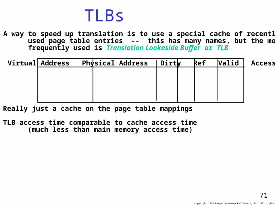
TLBsA way to speed up translation is to use a special cache of recently used page table entries -- this has many names, but the most frequently used is Translation Lookaside Buffer or TLB
Virtual Address Physical Address Dirty Ref Valid Access
Really just a cache on the page table mappings
TLB access time comparable to cache access time (much less than main memory access time)
Copyright 1998 Morgan Kaufmann Publishers, Inc. All rights reserved.
72
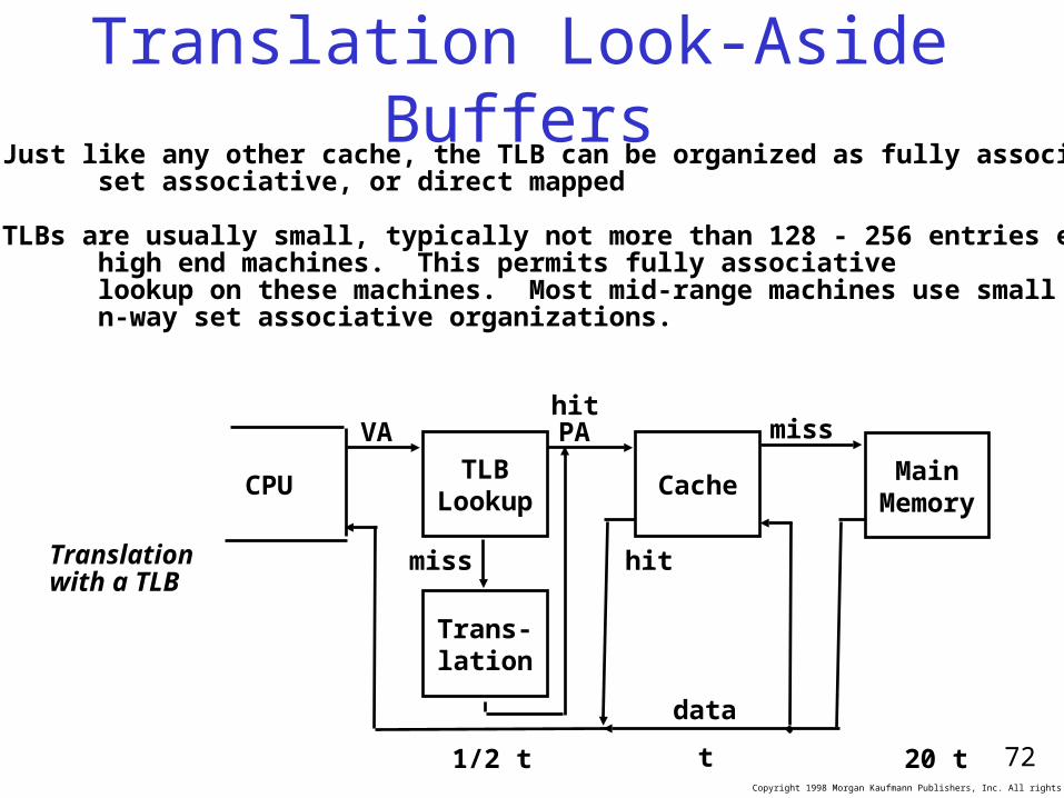
Translation Look-Aside BuffersJust like any other cache, the TLB can be organized as fully associative, set associative, or direct mapped
TLBs are usually small, typically not more than 128 - 256 entries even on high end machines. This permits fully associative lookup on these machines. Most mid-range machines use small n-way set associative organizations.
CPUTLB
LookupCache Main
Memory
VA PA miss
hit
data
Trans-lation
hit
miss
20 tt1/2 t
Translationwith a TLB
Copyright 1998 Morgan Kaufmann Publishers, Inc. All rights reserved.
73
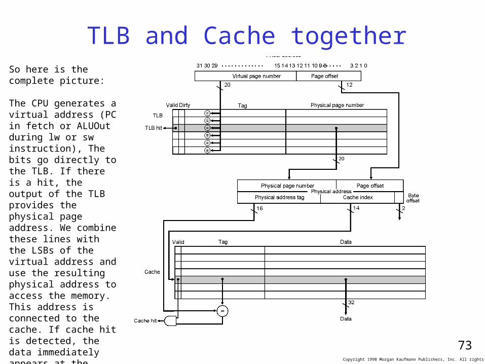
TLB and Cache togetherSo here is the complete picture:
The CPU generates a virtual address (PC in fetch or ALUOut during lw or sw instruction), The bits go directly to the TLB. If there is a hit, the output of the TLB provides the physical page address. We combine these lines with the LSBs of the virtual address and use the resulting physical address to access the memory. This address is connected to the cache. If cache hit is detected, the data immediately appears at the output of the cache.
All of this took less than a CK cycle so we can use the data in the next rising edge of the CK.
Copyright 1998 Morgan Kaufmann Publishers, Inc. All rights reserved.
74
Reducing Translation Time
Machines with TLBs go one step further to reduce # cycles/cache access
They overlap the cache access with the TLB access:
high order bits of the VA are used to look in the TLB while low order bits are used as index into cache
Copyright 1998 Morgan Kaufmann Publishers, Inc. All rights reserved.
75
ProtectionDuring the process of having a page fault we can detect that a program is trying to access a virtual page that is not defined. A regular process cannot be allowed to access the page table itself, i.e., read and write to the page table. Only kernel (OS) processes can do that. There can also be restrictions on writing to certain pages. All this can be achieved with special bits in the TLB (kernel bit, write access bit etc.). Any violation should cause an exception that will be handled by the OS.
In some OS and CPUs, not all pages have the same size. We then use the term segment instead of page. In such case we need to have h/w support that detects that the CPU tries to access an address which is beyond the limit of the segment.
Copyright 1998 Morgan Kaufmann Publishers, Inc. All rights reserved.
76
End of caches & VM
Copyright 1998 Morgan Kaufmann Publishers, Inc. All rights reserved.
77
Conventional Wisdom Changes!!
• CW1; Old; power is free, Transistors are expensive
new: Power expensive, Transistors are free
• CW2: O: If power concern, only dynamic power
N: Static power 40% of total, concern Leakage.
• CW7: O: Multiply is slow, lw & sw are fast
N: Multiply is fast, lw & sw slow (200 ck cycles to DRAM).
Copyright 1998 Morgan Kaufmann Publishers, Inc. All rights reserved.
78
Conventional Wisdom Changes!!
• CW10; Old; Don’t bother parallelizing, just wait
new: Too long wait. Go parallel.
• CW11: O: Increasing clock rate – the way to improve performance
N: Parallelism is the way to increase performance
Copyright 1998 Morgan Kaufmann Publishers, Inc. All rights reserved.
79
Direct Mapped Cacheblock = 1 word
size of cache=16words
Copyright 1998 Morgan Kaufmann Publishers, Inc. All rights reserved.
80
For MIPS:
Copyright 1998 Morgan Kaufmann Publishers, Inc. All rights reserved.
81
A fully associative cache
Here the block size is 2m word. We see that we have only N blocks
30-m 2
m
Tag
30-m
m
3232
32 32 32 3232
TagV
32
32 32 32 3232
TagV
32
32 32 32 3232
TagV
32
32
Copyright 1998 Morgan Kaufmann Publishers, Inc. All rights reserved.
82
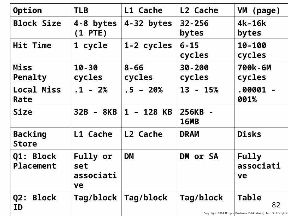
Option TLB L1 Cache L2 Cache VM (page)
Block Size 4-8 bytes (1 PTE)
4-32 bytes 32-256 bytes 4k-16k bytes
Hit Time 1 cycle 1-2 cycles 6-15 cycles 10-100 cycles
Miss Penalty 10-30 cycles
8-66 cycles 30-200 cycles 700k-6M cycles
Local Miss Rate
.1 - 2% .5 – 20% 13 - 15% .00001 - 001%
Size 32B – 8KB 1 – 128 KB 256KB - 16MB
Backing Store L1 Cache L2 Cache DRAM Disks
Q1: Block Placement
Fully or set associative
DM DM or SA Fully associative
Q2: Block ID Tag/block Tag/block Tag/block Table
Q3: Block Replacement
Random (not last)
N.A. For DM Random (if SA)
LRU/LFU
Q4: Writes Flush on PTE write
Through or back
Write-back Write-back
Copyright 1998 Morgan Kaufmann Publishers, Inc. All rights reserved.
83
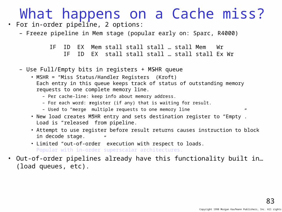
What happens on a Cache miss?• For in-order pipeline, 2 options:
– Freeze pipeline in Mem stage (popular early on: Sparc, R4000)
IF ID EX Mem stall stall stall … stall Mem Wr IF ID EX stall stall stall … stall stall Ex Wr
– Use Full/Empty bits in registers + MSHR queue• MSHR = “Miss Status/Handler Registers” (Kroft)
Each entry in this queue keeps track of status of outstanding memory requests to one complete memory line.
– Per cache-line: keep info about memory address.
– For each word: register (if any) that is waiting for result.
– Used to “merge” multiple requests to one memory line
• New load creates MSHR entry and sets destination register to “Empty”. Load is “released” from pipeline.
• Attempt to use register before result returns causes instruction to block in decode stage.• Limited “out-of-order” execution with respect to loads.
Popular with in-order superscalar architectures.
• Out-of-order pipelines already have this functionality built in… (load queues, etc).
Copyright 1998 Morgan Kaufmann Publishers, Inc. All rights reserved.
84
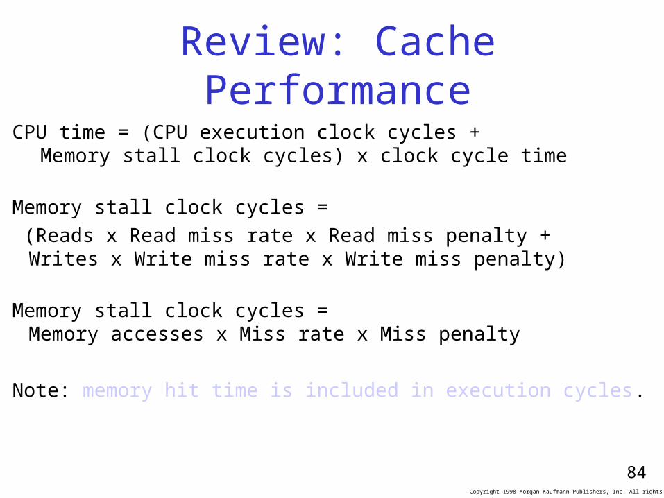
Review: Cache Performance
CPU time = (CPU execution clock cycles + Memory stall clock cycles) x clock cycle time
Memory stall clock cycles =
(Reads x Read miss rate x Read miss penalty + Writes x Write miss rate x Write miss penalty)
Memory stall clock cycles = Memory accesses x Miss rate x Miss penalty
Note: memory hit time is included in execution cycles.
Copyright 1998 Morgan Kaufmann Publishers, Inc. All rights reserved.
85
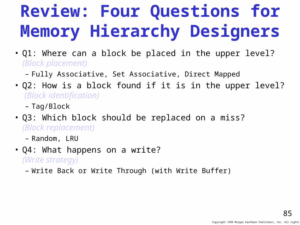
Review: Four Questions for Memory Hierarchy Designers
• Q1: Where can a block be placed in the upper level? (Block placement)– Fully Associative, Set Associative, Direct Mapped
• Q2: How is a block found if it is in the upper level? (Block identification)– Tag/Block
• Q3: Which block should be replaced on a miss? (Block replacement)– Random, LRU
• Q4: What happens on a write? (Write strategy)– Write Back or Write Through (with Write Buffer)